a digital recording system for space-based applications utilizing four-megabit ... ·...
TRANSCRIPT

Calhoun: The NPS Institutional Archive
Theses and Dissertations Thesis Collection
1985-06
A digital recording system for space-based
applications utilizing four-megabit magnetic bubble memories
Campbell, Bruce A.
Monterey, California. Naval Postgraduate School
http://hdl.handle.net/10945/21279


DUDLEY KNOX LIBF.ARY
NAVAL POSTGRADUATE SC
MONTEREY, CALIFORNIA 03 '3


NAVAL POSTGRADUATE SCHOOL
Monterey, California
THESISA DIGITAL RECORDING SYSTEM FOR SPACE-BASED
APPLICATIONS UTILIZING FOUR-MEGABITMAGNETIC BUBBLE MEMORIES
by
Bruce A. Campbell
June 1985
Thessis Advisor: R. Panholzer
Approved for public release; distribution is unlimited
1222819


SECURITY CLASSIFICATION OF THIS PAGE (TWl»n Data Entered)
REPORT DOCUMENTATION PAGE READ INSTRUCTIONSBEFORE COMPLETING FORM
1. REPORT NUMBER 2. GOVT ACCESSION NO 3. RECIPIENT'S CATALOG NUMBER
4. TITLE (and Subtitle)
A Digital Recording System For Space-Based Applications Utilizing Four-MegabitMagnetic Bubble Memories
5. TYPE OF REPORT h PERIOD COVEREDMaster's Thesis;June 1985
6. PERFORMING ORG. REPORT NUMBER
7. AUTHORS
Bruce A. Campbell8. CONTRACT OR GRANT NUMBERC*)
9. PERFORMING ORGANIZATION NAME AND ADDRESS
Naval Postgraduate SchoolMonterey, California 93943-5100
10. PROGRAM ELEMENT. PROJECT, TASKAREA a WORK UNIT NUMBERS
II. CONTROLLING OFFICE NAME AND ADDRESS
Naval Postgraduate SchoolMonterey, California 93943-5100
12. REPORT DATE
June 198513. NUMBER OF PAGES
1231*. MONITORING AGENCY NAME 4 AODRESSC// different from Controlling Ottlca) 15. SECURITY CLASS, (ol thlt report)
UNCLASSIFIED
15a. OECLASSIFI CATION/ DOWN GRADINGSCHEDULE
16. DISTRIBUTION ST ATEMEN T (ol this Report)
Approved for public release; distribution is unlimited
17. DISTRIBUTION STATEMENT (ol the abetract entered In Block 20, It dllterent Irom Report)
18. SUPPLEMENTARY NOTES
19. KEY WORDS (Continue on reverse aide II noceeaary and Identify by block number)
Bubble Memory; Magnetic Bubble Memory; Digital Data Recorder;Outer Space Data Recorder; Outer Space Digital Data Recorder
20. ABSTRACT 'Continue on reverae aide II neceeeary and Identity by block number)Magnetic bubble memory technology offers several desirable
characteristics for applications in space as a mass datarecording and storage system.
A modular combination of Intel Corp. state-of-the-art four-megabit magnetic bubble memory components is presented which canbe configured as a digital data recorder of variable capacityand input rate.
DD FORM1 JAN 73 1473 EDITION OF 1 NOV 65 IS OBSOLETE
S N 0102- LF- 014- 6601 1 SECURITY CLASSIFICATION OF THIS PAGe (When Data Bntarad)

SECURITY CLASSIFICATION OF THIS PAGE (Whan Df Enffd)
A description of magnetic bubble memory technology andoperation is included in an appendix.
S<N 0102- LF- 014- 6601
SECURITY CLASSIFICATION OF THIS PAGE(T»Ti»n Data Bnffd)

Approved For public release; distribution is unlimited
A Digital Recording Systemfor Space-Based Applications
Utilizing Four-Megabit Magnetic Bubble Memories
by
Bruce A. CampbellLieutenant, United States Navy
B.S. Aerospace Engineering, U.S. Naval Academy, 1977
Submitted in partial fulfillment of therequirements for the degree of
MASTER OF SCIENCE IN ELECTRICAL ENGINEERING
from the
NAVAL POSTGRADUATE SCHOOLJune 19 8 5

ABSTEACT
Magnetic bubble memory technology offers several desir-
able characteristics for applications in space as a mass
data recording and storage system.
A modular combination of Intel Corp. state-of-the-art
four-megabit magnetic bubble memory components is presented
which can be configured as a digital data recorder of vari-
able capacity and input rate.
A description of magnetic bubble memory technology and
operation is included in an appendix.

TABLE OF CONTENTS
I. INTRODUCTION 13
A. MAGNETIC BOBBLE MEMORIES AND SPACE
APPLICATIONS 13
II. A MAGNETIC BUBBLE MEMORY SYSTEM 18
A. THE FOUR-MEGABIT MAGNETIC BUBBLE MEMORY
MODULE 19
1. The 7114 Magnetic Bubble Memory Chip ... 21
2. The 7250 Coil Pre-Driver Chip and 7264
Coil Drive Transistors 23
3. The 7234 Current Pulse Generator Chip . . 24
U. The 7245 Formatter/Sense Amplifier
Chip 25
5. The Four-Megabit Memory "Module" 27
B. THE 7225 EUBBLE MEMCRY CONTROLLER 27
1. Bubble Memory Signals 29
2. External System Interface ........293. Parallel Controller Capability 30
4. Internal Operations 30
5. A Four-Megabit Magnetic Bubble Memory
System 32
C. MULTIPLE MEMORY MODULE SYSTEMS 32
1. Multi-Module Interfacing 32
2. Multi-Module Operations 33
D. THE EIGHT-MODULE MAGNETIC BUBBLE MEMORY
BOARD 37
1. Memory Capacity 37
2. Data Rates 38
3. Transfer Page Size 38

4. Power Consumption 38
5. Size/Weight 39
E. PARALLEL CONTROLLER OPERATION 42
III. MAGNETIC BOBBLE MEMORY SYSTEM OPERATION 44
A. BMC - EXTERNAL SYSTEM COMMUNICATIONS 45
1. Command/Status Fort 46
2. Register Address Counter 46
3. Parametric Registers 48
4. FIFO 53
5. Error Correction 53
6. BMC Status Register 56
7. Commands ....57B. NORMAL OPERATING PROCEDURES 59
1. Power-Dp and Command Execution 59
2. Power Down 62
IV. A MAGNETIC BUEELE MEMORY DIGITAL RECORDER .... 64
A. SYSTEM DESIGN LOGIC 64
1. Memory Capacity 64
2. Data Bate 64
B. N.P.S. PROTOTYPE DIGITAL RECORDER 66
1. Background 66
2. Experiment Description 66
3. Recorder Requirements 67
4. BPK 5V75A Prototype Kit Design 67
5. Multi-Kodule Custom Design -.68
APPENDIX A: MAGNETIC BUBBLE MEMORY TECHNOLOGY 71
A. MAGNETIC EUBBLE MEMORY CELL DESCRIPTION ... 71
1. Substrate ........712. Permanent Magnet 72
3. Location and Movement of Data Bubbles . . 73
4. Data Storage Organization 79
5. Data Eubble Production 81

6. Data Input 83
7. Data Cutput 84
8. Bubble Detection 84
9. Data Organization and Addressing 85
10. Memory Cell Components 86
B. MEMORY CEIL REQUIRED SUPPORT 87
1. Current Pulse Production 88
2. Input/Cutput Formatter 89
3. Controller 89
APPENDIX B: INTEL CCFP. MAGNETIC BOBBLE MEMORY
COMPONENTS 90
A. THE 7114 MAGNETIC BOBBLE MEMORY CHIP 91
1. Data Storage Configuration 92
2- Data Input/Output 9 4
3. Bcotlccp 95
B. THE INTEL 7250 COIL PRE-DRIVER CHIP AND
7264 COIL DRIVE TRANSISTORS 96
1. 7250 Coil Pre-Driver 96
2. 7264 Coil Drive Transistors 97
C. THE INTEL 7234 CORRENT POLSE GENERATOR
CHIP 97
D. THE INTEL 7244 FORMATTER/SENSE AMPLIFIER
CHIP 9 8
E. THE FOOR-MEGABIT MEMORY MODULE 103
F. THE 7224 CONTROLLER 104
1- 7224 BMC Internal Configuration .... 105
G. MULTIPLE MCDOLE SYSTEM CONFIGDR ATIONS ... 110
1. BMC - FSA Communications 110
H. OPERATING LIMITATIONS AND REQOIREMENTS ... 116
1. Operating Limitations 116
2. Voltace Regulator Circuitry 116
3. Powerfail Circuit 117
I. THE BPK 5V75A PROTOTYPE KIT 118
LIST Of REFERENCES 120
7

BIBLICGEAPHY 122
INITIAL DISTRIBUTION LIST 123
8

LIST OF TABLES
1. Bufcble Memory Comparison 15
2. Serial Memory System Operating Parameters .... 36
3. Eight-Module Memory Board Performance 39
4. Eight-Module Memory Board Power Requirements ... 40
5. Command/Status Port Functions 46
6. Register Address Counter Assignments 47
7. Memory Module Addressing Scheme 51
8. Error Correction Levels 55
9. EMC Command Set 58
10. 7114 MBM Pin-Out Signal Descriptions 93
11. 7250 CPD Pin-Cut Signal Descriptions 97
12. 7264 CDT Pin-Out Signal Descriptions 99
13. 7234 CPG Pin-Out Signal Descriptions 100
14. 7244 FSA Pin-Cut Signal Descriptions 102
15. FSA Command Codes 104
16. 7224 BMC Pin-Cut Signal Descriptions 106
17. 7224 BMC Pin-Cut Signal Descriptions (cont.) . . 108
18. 7114 Absolute Maximum Ratings 117

LIST OF FIGURES
1.1 Memory Technology Comparison 14
1.2 Cost per Bit vs. Access Time 16
1.3 Memory Capacity vs. Access Time 17
2.1 Buttle Memory System Components 20
2.2 7114 Magnetic Eubble Memory Chip Assemtly 21
2.3 7114 Magnetic Bubble Memory Chip Signals 23
2.4 7250 CPD and 7264 CDT Signals 24
2.5 7234 Current Pulse Generator Chip Signals 25
2.6 7245 Formatter/Sense Amp Chip Signals 26
2.7 7225 Bubble Memory Controller Signals 28
2.8 Four-Megabit Magnetic Bubtle Memory System .... 33
2.9 Multiple Memory Module System Configuration .... 34
2.10 Memory Module Approximate Area 41
2.11 Eight-Module Memory Board 42
3.1 7225 BMC - External System Interface 45
3.2 Block Length Register 49
3.3 Address Register 50
3.4 Enable Register 52
3.5 7224 Status Register 56
3.6 Memory System Power-Up Sequence ,.603.7 Memory System Initialization 61
3.8 Memory System Command Execution 62
3.9 Data Transfer Procedure 63
A.
1
Magnetic Substrate and Effects of an Applied
Perpendicular Magnetic Field 72
A.
2
Wide-Gap Permalloy Structure Designs 73
A.
3
Magnified View of Chevrons on Substrate 74
A.
4
Orientation of the Substrate and Magnets 75
10

A.
5
Rotating Magnetic Field Circuit and Waveforms ... 77
A.
6
Movement of Buttles Beneath a Permalloy
Structure Due to a Rotating Magnetic Field .... 78
A.
7
Single Loop Buttle Storage Architecture 79
A.
8
Major/Minor Loop Bubble Storage Architecture ... 80
A.
9
Bubble Generation for Input 82
A-10 Input of Data to a Storage Loop 84
A. 1
1
Output of Data from a Storage Loop 85
A. 12 Magnetic Bubble Detection Circuit 86
A. 13 An Exploded Vie* of a Memory Cell 87
A. 14 Magnetic Bubble Memory Required Systems 88
B.
1
7114 Magnetic Bubble Memory Chip Schematic .... 92
B.
2
Intel 7114 Bubble Memory Chip Data Organization . . 94
B.3 7250 Coil Pre-Eriver Chip Schematic 9 6
B.4 7264 Coil Drive Transistor Schematic 98
B.5 7234 Current Pulse Generator Chip Schematic .... 99
B.6 7244 Formatter/Sense Amp Chip Schematic 101
B.
7
72 44 Formatter/Sense Amp Internal Block Diagram . 103
B.8 7224 Bubble Memory Controller Chip Schematic . . 105
B.9 7224 BMC Internal Configuration Block Diagram . . 109
B. 10 Four-Megabit System Circuit Diagram 111
B. 1
1
Memory System Expansion - 112
E.12 BMC - FSA Communications 113
B. 1
3
Access and Command of Multiple Memory Modules . . 114
B.14 Multiple Module Data Transfers 116
B. 1
5
Voltage Regulator Circuit 118
B. 16 BPK 5V75A Prototype Kit 119
11

ACKNOWLEDGEMENTS
First, I would like to thank my ex-squadron skipper,
then CDR Richard Hulse, for allowing me to attend the Navy's
first Space Symposium in 1981. It was there I learned of
plans to initiate a curriculum in space systems engineering
at the U.S. Naval Postgraduate School and this advanced
information allowed me to be one of the first of three offi-
cers enrolled in the program. As a result, I have been
fortunate enough to have received orders to the U.S. Naval
Academy to begin classes there teaching this same subject in
which I am most interested and extremely happy to fce able to
continue to pursue.
Next, I would like to thank professor Rudolph Panhclzer
not only for the time he spent as my thesis advisor but also
for the active support he gave to the entire group of
students working on the project which we hope will fly
aboard the Space Shuttle in the near future. I would also
like to express my appreciation to all of the students
involved in the project, especially to Tina D'Ercole and Tom
Frey for keeping me abreast of the development of the proto-
type bubble memory recorder portion of the experiment.
Also, Dave Rigmaiden hasn't received half the credit he
leserves for his support. Without his direct assistance the
project may never have "gotten off of the ground".
Finally, I would like to thank Bev, Rhonda, Betty,
Larry, Deb, Mike, Beth, Jack, and my other family and
friends for their cards, letters, calls, and visits, which
kept me sane and motivated even though I don't like elec-
trical engineering.
"My head I'd be scratchin'
while my thoughts were busy hatchin'
if I only had a brain."
12

I- IHTBODOCTION
A. HAGSETIC BOBBLE HEHORIES AND SPACE APPLICATIONS
[Bef. 1] states that the desired characteristics for
space-based memory systems are non-volatility, versatility,
reliability and ruggedness, and cost effectiveness.
[Ref. 2 ] is more specific in stressing the importance of
radiation hardness and constraints on physical size, weight,
and power consumption of all space-based systems.
Many of the references surveyed for this paper describe
benefits offered by magnetic bubble memory systems for
applications in space. Most of these benefits are attribu-
table to the physical properties of magnetic bubble
memories.
The cost for placing a specific payload into space is
derived from both the weight and the volume of the system.
Magnetic bubble memories are light-weight, compact, sclid-
state digital data storage systems conf igureable in many
ways to fit different requirements in size and weight, as
well as performance.
Space is a harsh environment for which the solid-state
nature of magnetic bubble memory is well suited. Some memo-
ries, such as analog tape recording systems and disk /drum
units, have moving parts which may need lubricants, an
atmosphere, and a controlled environment for proper opera-
tion. Solid-state magnetic bubble memories have no moving
parts, are operable in the vacuum of space, and over a wide
range of temperatures. The relatively rugged solid-state
construction also allows easier design in withstanding the
shocks and vibrations experienced by space systems during
launch and maneuvers.
13

Ambient radiation and its effect on stored digital
information is another problem still under investigation
£Ref. 3]. While its associated support components are ordi-
nary solid-state elements routinely used in spac« today, the
data-storing magnetic bubble memory chip is surrounded by
permanent magnets, field-producing coils, and a shield to
isolate these strong magnetic fields from nearby systems.
This configuration makes magnetic bubble memory chips natu-
rally harder to radiation effects than ordinary solid state
memory components.
Memory system -
capacity (bytes)"
10K
Chip capacity
(bits)
Bubble memory
products
64KH00K
Micro-file
memory and
program
memo ry
Mi croprocessor
Bubblememory
Competitive EP.ROM
memories
TOOKi
in 10M-J—
256KHM >1M
M1n1-f11e
memory
&Floppy/disk Id o
E3 MT
cassette
File
memory
W)
Drum M,n1
disk
Figure 1. 1 Heaory Technology Comparison.
Power consumption is another major concern of space
system engineers. A magnetic bubble memory consumes power
only when data is being transferred or when the system is
being prepared for transfers. No power is required to main-
tain data within a nagnetic bubble memory system, unlike
Mi

systems using other sclid-state storage technologies such as
charged couple devices or random access memories- This
characteristic is especially attractive for space systems
which stcre recorded data for later transmission to a ground
station [Bef. 4] or for systems which must be capable of
retaining alterable instructions indefinitely for later
implementation at a deep-space destination [Ref- 5].
TABLE 1
Bubble Memory Comparison
ADVANTAGES DISADVANTAGES
Higher reliability
Non-mechanicalSmaller size
Faster access
Simpler interface
Media integrity
Bubble memoryvs Floppy disk
Stored data not
readily changed
Non-volatile
Mo'e bits per device
Reduced Doard space
Bubble memoryvs RAM
Slower accessSlower transfer rate
Programmability
More bits per device
Less board space
Bubble memoryvs ROM or PROM
Slower access
Slower transfer rate
Magnetic bubble memory systems have inherently slow
access times due to the physical arrangement of the data
storage architecture. This limits their usefulness in high-
speed data storage and retrieval, such as required in a
main-frame type computing system. However, magnetic bubble
memory systems provide an excellent means for mass data
15

recording and storage. The modular characteristics of
present magnetic bubble memory designs permit custom config-
uration to meet virtually any recording need in terms of
data input rates and memory capacities by varied combina-
tions of discrete mercery units.
110
COccUJa.
oo
10-'
id- 2
10" 3
10"<
10
BIPOLAR
10" 3
1
MOS
I
ceo !
BUBBLEFIXED-HEAD
DISK/DRUM
ACCESS GAP-
I
± 1
MOVING-HEADDISK
TAPE
J L
10-* 10-' 1 10' 10 2 103 10* 10
5
ACCESS TIME (MICROSECONDS)
Figure 1-2 Cost per Bit vs. Access Time.
Figure 1.1 illustrates the memory capacities associated
with different types of memory uses and indicates the
competitive memory systems within each type. The figure
suggests that, due to the modularity of this type of system,
magnetic bubble memories could be configured for use in all
these types of memory applications.
Table 1 lists bubble memory advantages and disadvantages
when compared with scne competitive memory systems.
The following figures compare magnetic bubble memory
technology with ether memory technologies using access time
16

,013
ion
IN
C
109
*a
IJ«*U
107
8
m>O1-
.c5
103
10
...
Fast Medium Slow
Out lea I
Fig. J
Drums
Oipol ar
Cassettes
10 10 io-4
,o"z
Access time 1n seconds
10'
Figure 1-3 Heaory Capacity vs. Access Tine.
as a cottmon denominator. Figure 1.2 [ Ref . 6] indicates
magnetic bubble memory comparative cost and figure 1.3
[Ref. 7] compares the expected performance of magnetic
bubble memories with ether memory systems. In both compari-
sons it is seen that magnetic fcubble memories fill a gap, in
terms of these performance measures, when compared to all
technologies in general use. However, not all these technol-
ogies are as suitable for space-based applications and none
offer as many benefits for such use as does magnetic bubble
memory.
17

II. A flAGHETIC BOBBLE MEHORY SYSTBH
Id 1979 Intel Corporation of Santa Clara, Ca. introduced
a digital data storage and retrieval system based on
magnetic bubble technology [ Ref . 8]. The system was capable
of storing up to one-megabit of digital information in a
single buttle memory chip with the aid of a family of compo-
nents performing support and interface functions.
Improvements, mainly in production techniques, allowed an
increase in storage capacity within the same storage area
[Eef. 9] and resulted in the recent release of a new family
of magnetic bubble memory components with a single bubble
memory chip capable of storing up to four-megabits of
digital information. This is the maximum single-chip
storage capability available in this technology today.
The advantage offered by the Intel magnetic bubble
memory chip family is the ease with which a magnetic bubble
memory system can be implemented. The elements of the
system can be combined to form modular components which may
be configured in many ways to provide different capabilities
in terms of data rate and storage capacity.
Early designs required the user to be concerned with
overseeing proper operation of the magnetic bubble system
internal functions as well as control of data flow into and
out of the memory [ Bef • 10]. Intel components feature a
dedicated bubble memory controller to perform these internal
functions independently and serve as a simple interface
between the memory and the external system.
This chapter introduces the Intel components which can
be used to design a magnetic bubble memory system. The
first section describes the individual components which make
up a magnetic bubble memory "module" capable of storing
18

four- megabits of digital information. The second section
describes the controller chip which coordinates memory
access functions within a module. Configurations associ-
ating multiple memory "modules" with a single bubble memory
controller are discussed in the third section. A four-
megabyte configuration, incorporating eight memory modules
and one bubble memory controller on a single board, is
described in the fourth section. This represents the basic
element used in the proposed design of a digital data
recorder for space-based applications presented in Chapter
U. The last section describes the capability for parallel
controller operations which enhances even further the
possible performance of the magnetic bubble memory system.
Appendix A presents an explanation of the basic opera-
tion of a magnetic bubble memory. It is assumed that the
reader is familiar with this information and only a func-
tional description of the role each component performs in
magnetic bubble memory system operation is presented in this
chapter. Appendix B contains a more detailed description of
the available Intel magnetic bubble memory components.
Readers should be particularly aware that this chapter
and the following proposed designs incorporate the expected
capabilities of the 7225 bubble memory controller and 7245
formatter/sense amplifier chips not yet available as produc-
tion components. This is explained more fully in the intro-
duction to Appendix E.
A. THE FOUR-MEGABIT HAGHETIC BOBBLE HEMOBY MODULE
Figure 2.1 depicts the Intel Corp. components used to
construct a magnetic bubble memory system capable of storing
four-megabits of digital information.
The components listed below the 7225 BMC combine to form
a memory "module" which represents the basic block of
19

1.0
1.26 7245 F S Al a.n"
0.3
7250 C PD 0.31
_u 1
0--42
\77t>4\ 0.23
CDT
7225 BMC Bueble Memory Controller
7114 i'i E ft fiAGNETIC EtlBBLE MEMORY
7234 C P G Current Pulse Generator
7245 FS A Formatter S ense Amplifier
7250 C P D Coil Pre-Driver
7264 CDT Coil Drive Transistor*
* EIGHT REQUIRED PER MODULE
Figure 2. 1 Bubble Meaory Systea Components.
storage capacity on which designs of systems with higher
capacities and capabilities are based. The module contains
a single bubble memory chip and support components which
must accompany each memory chip for proper operation.
Since the bubble memory controller may be associated
with multiple memory nodules, description of this component
is provided separately in the next section.
20

1 • The 111.4 Magnetic 3u bble Memory Chip
The 7114 magnetic bubble memory (n BK) chip contains
the substrate in which magnetic bubbles are stored, the
permalloy structures which determine bubble location, the
permanent magnets which ensure bubble stability, and the
perpendicular coils which control bubble movement. The
entire assembly is enclosed in a case designed to protect
internal and external components from stray magnetic fields
( Figure 2.2 ) .
SHIELD
PERMANENTMAGNET
COIL
BUBBLESUBSTRATE
PERMANENTMAGNET
Figure 2.2 7114 Magnetic Bubble Memory Chip Asseibly,
21

a. Data Organization
The major-track/minor-loop data storage archi-
tecture of the 7114 MEM consists of 512 storage "loops" with
8192 discrete locations per loop providing a maximum user
storage capability of 4,194,304 bits (four-megabits) of
digital information. This architecture requires transfer of
data in "pages" of 5 12 bits (64 bytes) of information each
input/output operation, corresponding to one bit of informa-
tion per storage loop. Each chip can store up to 8192 data
pages.
1. Bootloop and Error Correction Codes
Twenty-eight additional loops are used to store
twenty-eight bits of error correcting code appended to each
data page input to the memory for storage. Error correcting
capabilities are discussed in Chapter 3.
Two more loops contain the bootloop information
specific for each bubble memory chip. These loops contain a
digital representation of the operating loops within the
chip and a synchronization code which identifies th€ refer-
ence page from which all other stored pages are located.
This information is used by the support components to format
the data correctly for input and output operations and to
keep track of data flow and placement within the memory.
Figure 2.3 depicts the signals associated with
the 7 114 MBM. These signals are provided by or to the
support chips under guidance of the bubble memory controller
to perform the functions necessary for proper memory opera-
tion as described in Appendix A, namely: establishment of a
rotating magnetic field for bubble movement within the
memory, signals to generate data bubbles from seed bubbles
for input, swap and replicate signals for bubble movement
into and out of the storage loops, and detection of voltage
22

7234
CPG
. - .... _ .. _
7245
FSA
3 7114
MBM
REPLICATE \B00TL20P \GENERATE
SWAP /
BUBBLE \DETECTION /
V/
-==
PERPENDICULAR
FIELD COILS
7250/726^
cpd/ cdt
Figure 2.3 7114 Magnetic Babble Memory Chip Signals.
signals from the detector circuits for data output from the
memory.
The following subsections describe the support
components that perform most of these functions and which
must accompany each aemory chip for proper operation.
2. The 725 Coil Pre- Driver Chip, and 7264 Coil Drive
Transistors
Figure 2.4 depicts the 7250 coil pre-driver (CPD)
chip and the two sets of four matched 7264 coil drive tran-
sistors (CDTs) used to produce current signals sent to the
two perpendicular ceils surrounding the substrate material
within the 7114 MBM.
The 7250 CPD and 7264 CDTs produce triangular
current waveforms which are applied in quadrature to the
perpendicular coils based on timing signals from the bubble
memory controller. This establishes a rotating magnetic
23

7225
BMC
RESETI
7225
BMC
| PERPENDICULAR COIL
iTIflNG SIGNALS
7 A5 I
PERPENDICULAR COIL \
n jCURRENT SIGNALS /
|
/
cpd :/
I
CHIP
I SELECT
j
7245
FSA
/ZjU . CURRENT-\
/ 26-+ — 7254
i
7:54 H 7^!
-\X-COIL
DRIVE
CPD IIGNALS
7;ca ! : 7;c^
I 7254 72R K
r-coiL
DRIVE
8 - 7264
CDTs
7114
MBM
Figure 2.4 7250 CPD and 7264 CDT Signals.
field about the substrate which induces movement of stored
magnetic bubbles within the 71 14 MBM chip..
3 - She 72 34 Cur ren t Pulse Gener at or C hip
Figure 2.5 shows the signals associated with the
7234 current pulse generator (CPG) chip. Based on signals
from both the bubble memory controller and the formatter/
sense amplifier chip, the 7234 CPG sends current pulse
signals to the 7114 MBM which perform the generate, swap,
and replicate functions necessary during read and write
operations with the memory.
24

\ *
1
7114
MBM
7245
FSA
4.
3
4
CPS
TIMING, 3G0TLCCP \
SWAP. REPLICATE /
BC0TL3CP, 3ESEPATE \
SWAP, PE 0,_:CATE /
7225/
A
•
1 1
BMC / PowE'-'AIL t( SENEPATE, CHIP SELEC'I
\\1
Figure 2.5 7234 Current Pulse Generator Chip Signals.
The 7234 receives both the 5-volt ani 12-volt power
supplies required by the memory system and acts as a monitor
for these supplies. If either source falls below specified
thresholds (Appendix E) , a power-fail signal is sent to the
bubble memory controller to aid in deactivation of the
system in an orderly sequence to preserve data integrity.
1 • 2fe§ 22^5 Formatter/Sense Amplifier Chip
The 7245 1 formatter /sense amplifier (FSA) interacts
with each of the memcry components and performs a number of
functions concerned with data transfer within the system.
Figure 2.6 depicts the numerous signals associated with the
FSA and the other components involved.
a. External Signals
The bubble memory controller communicates with a
memory module through the 7245 FSA via a single
bi-directional serial data line (DIO)
.
The level of the
command/data (C/D) line specifies whether signals on the DIO
are to be interpreted as commands or data. Direction of
iThis section is hased on information about the existing7244 FSA chip and the expected capabilities of the 7245 chipas described in advance information provided by Intel. SeeAppendix E.
25

.... .. ....• — ~
7225 / prior NEXTbmc / 7245 7245
^ <>":elect in" \ '3ELECT "JUT* |
/1_i
it
5
FSA
'1
7111
MBM
7Z3<»
CPG
7250
\, '--^( BUB3l£ 3E*E:'l3NJ
7225
BMC
COMMAND/ DATA VTIMING, PESET /
CHIP ENABLE \GENERATE /
.i - <
<C SESIAL 3 10 NN — • CHI" ESABLE ^
V
. ...
Figure 2.6 7245 Formatter/Sense Amp Chip Signals.
data flow on the DIO depends on the received command which
dictates the memory operation to be performed. Ihe
controller also provides reset and timing signals and
responds to error signals generated if a 7245 FSA built-in
error correction scheme discovers a discrepancy during data
extraction from the memory chip.
The bubble memory controller enables operation
of a module and establishes communication with the FSA using
the chip "select in" line. In multi-module configurations,
this chip select signal is passed from module to module to
establish a time-multiplexed communication between the
bubble memory controller and each module FSA individually.
This process is discussed again later in this chapter and
explained in detail ir Appendix B.
Bubble generate signals are sent to the 7234 CPG
in proper sequence for data input to the memory. Millivolt
signals from the buttle detection circuits are sensed and
amplified during a memory read and reconstructed intc the
original data stream for output.
The 7245 also produces enable signals to the
7234 CPG and 7250 CPD chips. These components and the
current supply to the 7114 MEM detection circuits are only
26

enabled when required by the memory access operation. This
reduces power consumption during times the system is not
actively transferring data.
t. Internal Operations
The 7245 FSA is prepared for up-coming opera-
tions by the input cf a four-bit command code sent by the
bubble memory controller over the serial data line, with the
appropriate level on the command/data line. The commands
include initialize, reset, and memory read and write opera-
tions as well as specifying the error-correction scheme and
checking cf the FSA status register.
Data are passed through a 540-bit first-in/
first-out (FIFO) buffer where 28 bits of error correcting
code are appended or checked for each entire 512-bit page of
data transferred.
Another register holds the bootloop information,
extracted from the memory chip, used to correlate data with
operating storage loops during input and output operations.
5- The Fo ur-Megabit Memor y " Module"
The components described above can be combined to
form the basic block cf memory storage capability which will
be referred to as a memory "module". Each module is capable
of transferring and storing up to four-megabits of digital
information under guidance of a bubble memory controller.
The controller, which may be associated with multiple memory
modules, is described in the next section.
B. THE 7225 BOBBLE BEHOBY CONTBOILEB
Use of a dedicated device to control the internal func-
tions required within the magnetic bubble memory system is
an improvement over early designs in which the user was
27

required to incorporate these functions into the overall
operation of the system utilizing bubble memory. Intel
components allow the designer to access the memory in much
the same way as conventional memory systems, leaving actual
operation of the bultle memory subsystems to the dedicated
controller.
This section presents the 7225 2 bubble memory controller
(BMC) and briefly describes the signals produced to control
the functions of a butble memory module, and the interface
the controller presents to the external system accessing the
bubble memory. These signals are depicted in Figure 2.7.
EXTERNAL
SYSTEM
INTERFACE
CHIP SELECT, RESET \
READ, WRITE
DMA DATA ACK. /
Ao REGISTER ACCESS
VA-
INTESRUPT
On* DATA REO.
-\
/ 3-SIT PORT\—— /
7225
BMCWAIT
RESET
TIMING
[N 7245. 723U. 7250
\ 725—y cpc
'50
cpo
PCwER-fAIL
TIMING, 3O0TLOOP
SWAP, REPLICATE
COMMAND/ DATA,
TIMING
C^ IAL DIO
PARALLEL
7225
BMC
7234
CPG
72^5
FSA
Figure 2.7 7225 Bubble Memory Controller Signals.
2 This section is based on information about the existing7224 EMC chip and the expected capabilities of the 7225 chipas described in advance information provided by Intel. SeeAppendix B.
28

1 . Bubble Memory Signals
Descriptions of the signals that pass between the
controller and support chips have been provided in the
component descriptions of the last section. Figure 2.7
summarizes the memory component control signals associated
directly with the bubble memory controller. Most important
are the critical tining signals provided to coordinate the
bubble memory functions with respect to movement of the
magnetic bubbles with the rotating magnetic field. The
controller also exchanges command, status, and data signals
to the memory module via the 72U5 FSA, and produces swap and
replicate signals and receives power-fail indications
directly with the 7234 CPG.
2- External Sy_stem Interface
The interface to the external system consists of
memory access function lines and an eight-bit data bus as
shown in the figure. The function lines are compatible with
other Intel controllers and their interconnections with
other types of data storage systems. The user must send
specific bubble memory commands over the interface tc the
bubble itemcry controller to prepare the system for data
input or output before each accessing operation. Chapter 3
discusses the interaction process required by an external
system in accessing a magnetic bubble memory.
When these commands are received, the BMC generates
the required signals to the memory cell components to
perform the operation with no further intervention by the
external system required besides the necessity to provide or
accept data at a known rate.
The external system can either transfer data
directly with the BMC using a polled status mode tc coordi-
nate data flow, or incorporate a direct memory access (DMA)
29

system to manage handshake protocol with the BMC separately.
The polled mode is simpler to incorporate but requires
constant attention by the external system to manage data
flow. EHA relieves the external system of this requirement,
but incorporates additional hardware and increases system
complexity. The method employed would depend on the partic-
ular application (required data rate) and the specific
external system involved.
The process of determining the operational memory
configuration best suited for a particular recording need is
outlined in Chapter 4. A sample system is presented in
Chapter H as well, tut since there are many external system
configurations which could provide the required interface to
the magnetic bubble memory, no specific discussion of
external systems or suggested data transfer method is
presented in this paper.
3 . Parallel Con troller Capability
The "wait" signal is used to coordinate the actions
within a magnetic bubble memory system using two 7225 BMCs
actively transferring data simultaneously in parallel. The
advantage of this capability is discussed later in this
chapter.
ti " Int ern al Operations
Internal operations of the bubble memory controller
are described in detail in Appendix B. However, certain
aspects of the internal configuration of the chip must be
presented here in order to understand the system operation
described in the next chapter. These aspects are also
important to expansion of the system into a larger capacity
configuration.
30

a. Power Failure, Abort, and Reset Logic
In the case of a power failure detected by the
7234 CPG or an externally-generated abort/reset signal, a
routine is automatically initiated to de-activate the memory
module in an orderly fashion to ensure data integrity within
the magnetic bubble memory chip.
i. Internal Registers
A number of registers are accessed by the
external system to prepare the memory system for operations.
The registers specify the operation to be conducted, the
amount of data to be transferred, the memory module and
location within to be accessed, and the method to be used in
the transfer. A register is also used to report the status
of the operation and the occurance of any errors or compli-
cations. The registers are accessed via the eight-bit port
using specific signals sent by the external system over the
memory access lines. Operation of the bubble memory system
includes frequent interaction with the BMC registers and
this important process is described more fully in the next
chapter.
c. FIFO
The 7225 BMC FIFO is a 128 x 8 bit first-in/
first-out RAM used as a data buffer between the bubble
memory and the external system. The magnetic bubble memory
chip transfers data only in 64-fcyte blocks ("pages") , thus a
full EMC FIFO may contain enough data at any one time for
two complete transfers to a single memory module. Data are
transferred between the BMC FIFO and the memory system at a
fixed rate depending on the number of modules within the
system. The average data transfer rate to a single memory
module is 16 kbytes per second, two modules in parallel
31

require 32 kbytes per second, etc. The BMC FIFO relieves
any small differences in data transfer from the external
system to the memory as long as the difference does not
eventually deplete or overflow the data buffer before the
operation is complete.
5. A Four-Megabit Magnetic Bubble Memorv System
Figure 2.8 is a block diagram of a complete magnetic
bubble memory system capable of storing up to four- megabits
of digital information. The figure depicts the basic inter-
connections between a single memory module and the bubble
memory controller which also serves as the interface to the
external system accessing the bubble memory system. Though
not labelled, the arrows between components represent the
same associated signals as described earlier in this
chapter.
C. HOITIPLE HEMOBT 1CD0LE SYSTEMS
1 • Multi-Module Interfacing
Figure 2.9 stews how the basic system of Figure 2.8
is expanded to incorporate multiple memory modules into a
system controlled by a single 7225 bubble memory controller.
As can be seen, each module in the system receives the same
BMC signals as are sent to a single module with the addition
of a signal sent between the FSAs themselves. This signal
establishes the time- multiplexing of the FSAs that allows
the bubble memory controller to access multiple memory
modules in a logical manner. This method of communication
between the bubble memory controller and multiple FSAs is
described in detail in Appendix B. Basically, the time-
multiplexing scheme allows the BMC to establish communica-
tions with any single memory module, or with several
combinations of modules in parallel operation, without
32

r
EXTERNAL
^-MEGABIT MODULE
Figure 2-8 Four-Hegabit Magnetic Bubble Hemory Systea.
experiencing contention over the command and data lines
common to all the modules. This communication scheme also
accounts for the system performance characteristics associ-
ated with the different multi-module configurations
presented next.
2- Multi-Module Operations
A single bubble memory controller physically
connected to multiple memory modules is capable of accessing
the modules in a number of ways, each of which produce
different performance of the system in terms of data
33

EXTERNAL SYSTEM
>*-'
7225 Brie
723<l 7245 7250
SUBSEOUFNT MODULES
r
Aiy
:;[
V ,
X fi^r
7245FSA '
IT
7234 CPG
1 1 II
7114
MBM1
l/
4-MECABIT MODULE
r
_i\
L L*'7wrL "J
'(-MEGABIT MODULE I
Figure 2.9 Multiple lienor y Module System Configuration.
34

transfer rates. System capacity, of course, is determined
merely by the number cf memory modules incorporated.
a. Serial Operation
Serial accessing of memory modules by the bubble
memory controller involves use of only a single memory
module at a time for a given operation. The BMC establishes
communication with the specific module FSA only, which in
turn enables the other components within the module as
required for data transfers. Other modules in the system
are in a stand-by mode and ignore the BMC signals sent out
over the lines ccmmon to all the memory modules.
Since only a single bubble memory chip is being
accessed, each transfer operation requires a minimum block
of 512 data bits (64 bytes) , corresponding to one data bit
per storage loop within the 7114 MBM, for a single page data
transfer with the system. Multiple-page transfers may be
specified by the command received from the external system
for a given operation and would involve exact multiples of
this 512-bit data block. Average data transfer rate between
the BMC and a single PSA is 16 kbytes per second.
Table 2 lists the important operating parameters
for single module (serial) system operation. This is the
performance of a single operating module even if it is part
of a multiple-module system. The power requirements stated
are based on a prototype kit provided by Intel and actual
power reguirements would probably be lower for a custcm-
designed system. A nodule on standby would be powered but
not actually in the process of transferring data (active).
Since magnetic bubble memory is non-volatile, data will be
maintained within the system even if all power is removed.
35

TABLE 2
Serial Heaory Systea Operating Parameters
Single transfer page size 512 bitsAverage (sustained) data rate 16 kbytes/secPower requirements (typical)
Active 6.5 WStandby 2.4 WNote: No power required for data storage only
b. Parallel Operation
By addressing more than one of the FSAs in the
multiple memory module system, the bubble memory controller
increases the amount of data that must be transferred each
operation, and increases the rate at which the transfer
occurs.
Combinations of two, four, and eight modules can
be accessed simultaneously resulting in average data
transfer rates which are multiples of the rate associated
with a single operating module.
Since data are being transferred to multiple
magnetic bubble memory chips simultaneously, the minimum
block cf data required for each transfer operation is also a
multiple of the 512-bit (64-byte) page size required by a
single 7114 MBH.
Power consumption changes with multiple module
configurations as well. The power consumed depends on the
cumber of modules in the system, and on the number of
modules actively engaged in data transfer or in the inactive
stand-by mode.
36

Description of specific multi-module perform-
ances are withheld until the next section which describes
the optimum physical combination of the bubble memory compo-
nents described to this point.
B. THE EIGHT-HOBULE BAGNETIC BOBBLE HEMOBY BOABB
A single 7225 BMC is capable of providing signals to up
to eight memory modules simultaneously. While smaller phys-
ical combinations are possible, the eight-modules per
controller configuration offers the user more flexibility of
operation than any other possible configuration. This
configuration also represents the optimum combination of
elements in terms of volume and weight which is a critical
factor in space systems designs. For these reasons, discus-
sions of digital data recorder designs presented in Chapter
4 specifically involve an eight memory modules per single
controller configuration.
Physical connection to eight memory modules allows the
controller to access the available memory systems in a
number of ways to achieve a desired performance in terms of
data transfer rate or memory capacity. The operational
configuration chosen is dictated mainly by the desired data
transfer rate. Expansion of any such system to meet
increased storage capacity requirements involves simple
incorporation of additional controller/module combinations
to the existing system. This procedure is demonstrated in
Chapter 4.
The following subsections summarize the performance
parameters of an eight- module magnetic bubble memory system.
1 . jjemory Capacity
Eight four-megabit chips offer a user data storage
capability of 4,194,304 bytes (eight-megabytes) or
33,554,432 bits of digital information.
37

2. Data Rates
Serial (individual) operation of the memory modules
transfers data at an average sustained rate of 1 6 kbytes per
second.
Parallel operation multiplies this rate by the
number of active modules resulting in transfer rates of 32,
64, or 128 kbytes/sec corresponding to the 2, 4, or 8 simul-
taneously operating nodule configurations possible. The
operating configuration chosen is determined by the maximum
data input/output rates expected with system operation.
The desired transfer rate is easily changed by the
external system through the commands and operation specifi-
cations sent to the bubble memory controller via the
external interface. This process is described in the next
chapter.
3- Transfer Page Size
512 bits, corresponding to one bit for each storage
loop, must be transferred into or out of each active memory
module for a single transfer operation. Parallel module
operation multiplies this page size by the number of modules
involved in the transfer.
Table 3 summarizes the data transfer rates and
minimum data page size reguired for a single transfer opera-
tion for each of the possible operating configurations of an
eight-nodule memory system.
U . Po wer Consumption
As was indicated in Table 2 , a single memory module
actively engaged in data transfer consumes about 6.5 watts.
Again, this is based on data available for an Intel- produced
prototype kit and power reguirements for a configuration as
described herein would probably be somewhat lower. A single
38

TABLE 3
Eight-Hod ule Memory Board Performance
Number of modulesoperating in parallel
Data rate (kbytes/sec)
Page size req. (bytes)
16
64
32
128
64
256
8
128
512
module on stand-by, (ie. powered but not involved in data
transfer) , consumes about 2.4 watts-
Eased on the information above, Table 4 lists the
expected power reguirements of an eight-module memory board
in its different operating configurations.
5 . Siz e/Weight
Figure 2.1 at the beginning of the chapter depicted
the size of the major components of the magnetic bubble
memory system. Figure 2.10 shows the estimated size of a
single memory module. The area shown in the figure is a
good estimate of the space required by an entire module
system including circuit elements such as resistors and
capacitors not illustrated. The layout in no way suggests
that this is the recommended positioning of the elements
within a module. [Bef. 11] outlines suggested board layouts
for single and multiple-module configurations for the one-
megabit nagnetic bubble memory system which is similar to
the four-megabit system in most respects.
39

TABLE 4
Eight-Hodule Beaory Board Power Requirements
Number cf modules Number of modules Poweractive stand-by required
8 19.2 \1
1 7 23.3 H
2 6 27.4 H
4 4 35.6 W
8 52.0 W
The 7264 coil drive transistors represent the
"tallest" components in the system, extending approximately
4/5 inches from the surface of the board. Based on this
information, it is estimated that an entire eight-module
memory board could measure approximately 8" x 18" as shown
in Figure 2.11. Multiple-board systems would require about
1-inch spacing.
The "board circuits" indicated on the figure irclude
a voltage regulator circuit to ensure voltage levels within
specified limits (Appendix B) , circuitry to assist in power-
fail detection, storage devices to maintain sufficient
voltage levels after a power failure to implement the shut-
down procedure, and ether memory board support circuitry as
may be required such as line drivers to ensure adequate
strength of the controller signals on the common lines to
all the modules, etc..
The weight of the board assembly has been estimated
from the available EPK5V75A prototype kits (Appendix B)
40

5
CP3
7245 FSA
7234 CPG
1
3 - ?:^Cjt*
Figure 2. 10 Heaory Module Approximate Area.
which weigh 9.7 oz. each. Allowing for the weight of the
extra ccnponents on the prototype kit not required od the
memory board, the expected weight of an eight-module memory
hoard would be approximately 43 oz. or less than three
pounds.
It is the configuration depicted in Figure 2.11 ,
and the operating parameters presented above, on which the
discussion of a digital data recorder for space-based appli-
cations presented in Chapter 4 is based.
41

MODULE
nMODULE MODULE
#5
MODULE
hoa
C
r '
5 '
I i
s
I
. . L . .
MODULE MODULE
mMODULE
#6
MODULE
#8
A
-- 8"
18"
Figure 2.11 Eight-Module Memory Board.
E. PARALLEL COHTEOLIEH OPERATION
As was shown earlier in Figure 2.7 , the 7225 BMC has an
output line labelled "wait" which can be used to coordinate
the operations between two bubble memory controllers working
in parallel. The twc BilCs may operate two separate memory
systems simultaneously to offer the user a 16-bit external
interface capability. This would double the operating
performances described for the system configurations
described earlier.
The "wait" signal between the bubble memory controllers
is used to ensure simultaneous operation of the systems
during data transfers. In the case of a transfer delay due
to a discovered data error (Chapter 3) or a power failure or
reset signal within cne of the memory systems, the signal
would te passed from the delayed controller to the other
system to inhibit further data transfer until the delay is
corrected and simultaneous operation can be re-established.
42

Parallel system operation could be the topic of another
bubble memory system study at the Naval Postgraduate School
and will not be considered further in this paper.
43

III. HAG1ETIC BOBBL E MEHOHY SYSTEM OPERATION
This chapter describes the basic interactions between an
external system and the bubble memory controller required
for communication and data transfer. The information
presented is a summary of information provided in [Be£. 12]
and specifically emphasizes the procedures pertinent to a
multiple memory module system as described in the last
chapter operating as a digital data recorder. Though
[Bef. 12] is provided as a guide to users implementing the
BPK5V75A four-megabit Intel prototype kit, familiarity with
the information therein is imperative before attempting to
formulate the operating routines to be implemented by any
external system utilizing the Intel four-megabit magnetic
bubble memory systems in any operating configuration.
The routines formulated depend on the external system
and data transfer method implemented as well as on the
number cf modules in the system. While no particular system
or method is specified in this paper, differences in opera-
tion due to these factors is presented as they occur in the
discussion.
Basically, the external system accesses the memory by
sending specific operating parameters and command codes to
the bubble memory controller which then produces the
internal signals necessary to conduct the desired operation.
If the operation involves data transfer, the system must
provide or accept data at the rate and in the quantity that
is specified by the operating parameters provided to the
bubble memory controller by the external system prior tc the
operation.
The first section presents the method the external
system uses to initiate the available functions of the
44

bubble aemory systen:. Combining these functions into a
working operating routine is discussed in the following
sect ion.
A. BBC - EXTEBHAL SISTEM COMMUNICATIONS
The last chapter described the physical connection
between the 7225 BMC and an external system as consisting of
an 8-bit data bus ar.d a number of memory access function
lines. Figure 2.7 is repeated here to emphasise the
external system interface. The interface shown is the same
whether the BMC controls a single memory module or many.
EXTERNAL
SYSTEM
INTERFACE
CHIP SELECT, RESET \
HEAD, ««!TE
3HA DAT* ACK.J
Ao REGISTER ACCESS
f
{
lNTE^SUPT
CMA DATA RE3.
_\
V 3-3IT PCRT
/
7225
BMC•AIT
PESET
T I M I sr,
'\72HS. 7234,
—
y
y c
7250
50
CPQ
/ ?C»£S--» 1L
TIMING, 3C0TL0QP
SWAP, PE°LICATE
CCPHAnO/CATA,
TIDING
7234
CPG
7245
FSA
SERIAL 310
PARALLEL
7225
BMC
Figure 3. 1 7225 BBC - External System Interface.
45

1. Command/Status Port
The command/status port consists of the 8-bit data
lines, the AO line, and the (separate) read (RD) and write
(PR) lines as shown in table 5. Notice that the 8-bit data
bus D4 bit line also plays a role in BF!C communications.
TABLE 5
Coaaand/Status Port Functions
Funct ion D7 D6 D5 DA D3 D2 Dl D0 RD/WR 00
Command d C 1 C C C C WR 1
ROC R R R R WR 1
Status S 5 S S S S S S RD 1
Access to the port is selected when the AO line is
set to a logical "1". The three possible locations accessed
are differentiated by the level of the D4 bit and the read
(RD) or write (WR) lines. Functional description of these
locaticns is presented next.
2« Register Address Counter4
Since description of their purposes explains much
about operation of the memory system, the register address
counter and its associated registers are discussed first.
With A0=1, E4=0, and WR=1, 3 the external system
gains access to either the BMC parametric registers or the
BMC FIFO, depending en the address on the D3-D0 bit lines of
^The external system will usually incorporate anencoding or hardware logic to ensure that the RD and WRlines are never set high simultaneously, as this wouldprovide conflicting signals to the bubble memory controller.
46
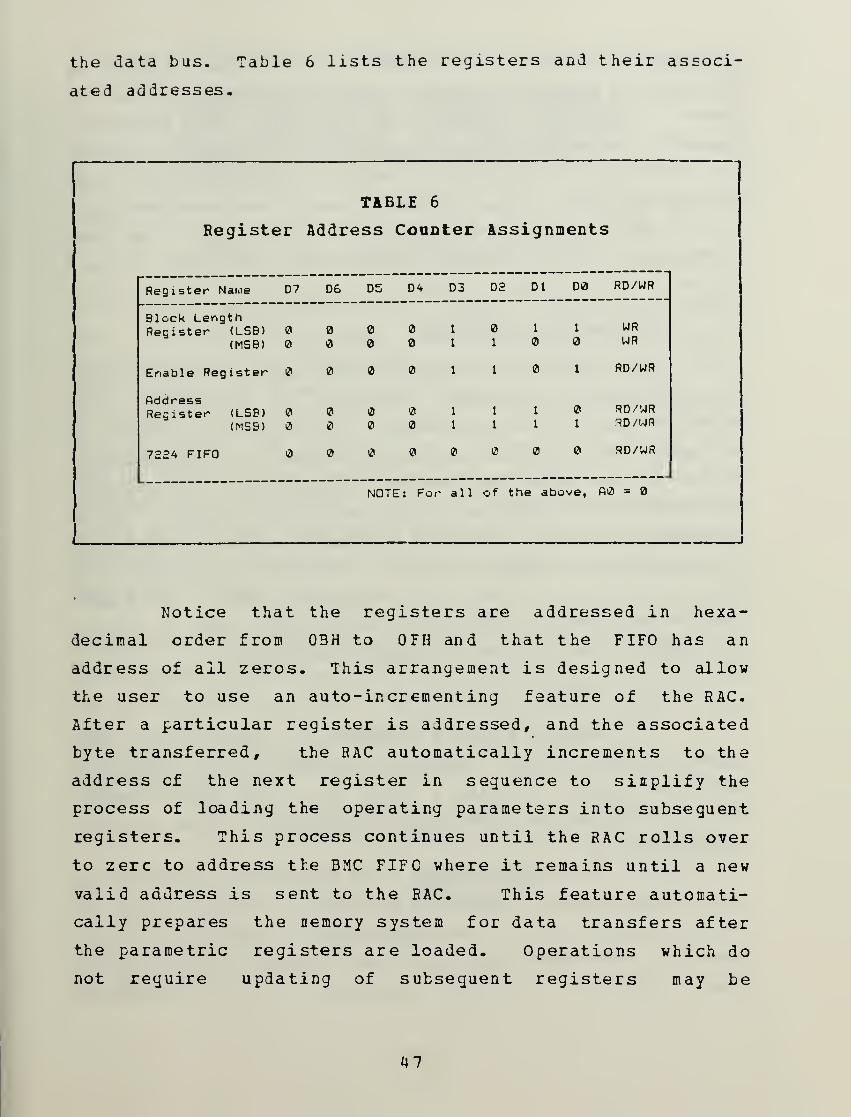
the data bus. Table 6 lists the registers and their associ-
ated addresses.
TABLE 6
Register Address Coaster Assignments
Register Name D7 D6 D5 D4 D3 D2 Dl D0 RD/WR
Block LengthRegister (LSB)
(MSB)
1
1 1
1 1 WRUIR
Enable Register i? 1 1 1 RD/WR
AddressRegister (LSB)
(MSB)i3 1
1
1
1
1
1 1
RD/WRRD/WR
7224 FIFO RD/WR
NOTE: For all of the above, A0 =
Notice that the registers are addressed in hexa-
decimal order from 03H to OFH and that the FIFO has an
address of all zeros. This arrangement is designed to allow
the user to use an auto-incrementing feature of the RAC.
After a particular register is addressed, and the associated
byte transferred, the RAC automatically increments to the
address of the next register in sequence to siiplify the
process of loading the operating parameters into subseguent
registers. This process continues until the RAC rolls over
to zerc to address the BMC FIFO where it remains until a new
valid address is sent to the RAC. This feature automati-
cally prepares the nemory system for data transfers after
the parametric registers are loaded. Operations which do
not require updating of subseguent registers may be
47

performed as well, but require the external system to
address the desired registers and FIFO separately as needed.
After a specific register (or the FIFO) is addressed,
lowering the AO line allows data transfer with the register
(or the FIFO on a bit-by-bit basis) depending on the level
of the read (RD) or write (WR) lines. Note that the block
length register may only be written into while the bytes
associated with the ether parametric registers may be read
by the external system as well.
3- Parametric Registers
The parametric registers are used by the external
system to specify the memory module (s) to be accessed, the
amount of data to be transferred, the method of transfer to
be used, and any error correcting scheme to be implemented.
Normal system operation involves transfer of the operating
parameters to the parametric registers (if required by the
upcoming operation) followed by issuance of the command code
to be executed. Once a command is issued to the BMC, the
parametric registers Bust not be modified until the opera-
tion is completed or terminated as they are used as working
registers by the BMC during command execution.
a. Block Length Register
The block length register is made up of a least
significant byte (LSB) and most significant byte (MSB) as
addressed through the RAC ( Table 6 ) . The bubble memory
controller interprets the data in these two bytes as shown
in Figure 3.2.
(1) Channel Field. Bits D7-D4 of the MSB are
known as the channel field and specify the number of FSAs to
be accessed during the next operation. Each FSA has two
channels associated with each half-system of the bubble
memory chip it services (Appendix B) . To preclude
48

•IOC* LENOTH MOISTEN MSS BLOCK LENQTH MEOISTER L3»
1 2
NUMSEM O* HACHANNELS <N*Q
NUMSEM C# PAGES TO It TWANSfEAREO
Figure 3.2 Block length Register.
asynchronous operation of the channels within the memory
chip, only one of the channel field bits may be set during a
given operation. A channel field entry of 0001 would select
enly a single FSA (memory module) for the next operation. A
0010 entry would specify parallel operation of two modules
simultaneously. The entries 0100 and 1000 would call for 4
nodule and 8 module operations respectively. A channel
field entry of 0000 will allcw half-system operation of a
memory module, but this operation is included for diagnostic
purposes only and is not a useful configuration in normal
memory operations.
Thus, the entry in the channel field speci-
fies the data transfer rate which will occur during the next
data transfer operation, as well as the page size required
for each single transfer. The channel field entry is also
used to specify the particular memory module (s) to be
addressed when combined with the MBM select field which is
described shortly.
(2) Terminal Count Field. The D2-D0 bits of
the USB and the eight LSB bits combine to form the terminal
count field. The eleven bits of this field are loaded with
the binary number of total pages to be transferred during
the next operation. This field limits the number of pages
that may be transferred during a single commanded operation
to 2048 pages.
49

t. Address Register
The address register also consists of a least
significant byte (LSB) and most significant byte (MSE) . The
BMC interprets the data in these two registers as shown in
Figure 3.3.
AOORESS RCQISTtN MSI AOOAESS MOISTEN LSI
MBM SELECT
El [1 2 1 I11111
STAftTlNQ AOORESS WITHIN EACH MSM
Figure 3.3 Address Register.
C) Starting Address Field. The address
register MSB D4-D0 Lits and the eight bits of the LSE are
interpreted as the logical page address within the memory
module (s) at which the transfer operation will begin. The
thirteen bits allow direct addressing of any of the modules*
8,192 storage pages. As each page of data is transferred,
the starting address field is incremented to automatically
select the next sequential page.
(2) MBM Selec t Field. Bits D7-D5 of the
address register MSB are called the MBM select field. This
field, along with the block length register channel field,
specify the particular memory module or group of modules to
be accessed. Table 7 illustrates this process.
For example, an MBM select field entry of
000 with a channel field entry of 0001 would address FSA
channels and 1 which are associated with the first iremory
module in sequence. An MBM select field entry of 00 1 with a
channel field entry of 0010 would specifically address the
50

TABLE 7
Memory Hodule Addressing Scheme
MBM Select Channel Field(Address (Block Length Reg ister MSB bits)
Reg isterMSB bits) 0000 0001 0010 0100 1000
0,1 0,1,2,3 a to 7 0toF1 1 2,3 4, 5, £,7 a to f
1 2 4,5 Q,9,ft,B
1 1 3 6,7 C.D, E, F
1 4 8,91 1 5 ft, B
1 1 6 C,D1 1 1 7 E, F
second and third meacry modules in sequence and call for
parallel operation.
A useful feature of the address register is
that when the starting address field increments past 8 r 192 ,
the MEM select field is automatically incremented as well to
select the next seguential memory module or group of
modules.
The address register (s) cay be read by the
external system. This allows the system to determine the
stopping address within the memory for a recording operation
of unknown length, and to specify the next page address as
the starting point for the next recording operation.
c. Enable Register
The enable register specifies the data transfer
method to be implemented, enables interrupt options, and
specifies the actions the system will perform in the occu-
rance of a detected data error. Each of the enable register
tits shown in Figure 3.4 and their associated functions are
discussed briefly.
51

CNAIlt MOISTtA
33INTIfMUPT IH»ilt !*OAM»U
_•> DM* (NASI.I
-» xtscwvro
-«• WKITC tOOUOOP INMlt-» tNtllf HCO
-» INAIlt ICO
-» f Kilt ( f ftMITT INTtMUPT
Figure 3.4 Enable Register.
M) Interrupts. The bits D7 , D1, and DO
enable the bubble memory system to produce an interrupt
signal to the external system under certain conditions. The
"normal" interrupt and the "parity" interrupt will not be
incorporated in future Intel modifications of the systems.
The external system should ensure that these bits are set to
"0" each time the enable register is loaded.
The "error" interrupt enable bit (D1) is
used in coordination with the read corrected data (RCD) and
internally corrected data (ICD) bits (D5 and D6) to specify
the level of error correction the system will implement and
the actions the system will perform when an error is
detected by the system FSA (s) . The write bootloop enable
bit is used to enable an external system to input data into
the memory systems* bcotloops. This action will not normally
be taken by the user so the external system should also
ensure that this bit is not set when loading the enable
register. The D3 bit was associated with a function avail-
able with the one- megabit system and is reserved in the
four-megabit systems. It also should be set to at all
times. Finally, the DMA enable bit (D2) when set allows the
EtfC to use its DRQ and DACK lines to establish a DMA hand-
shaking protocol during data transfers with the external
52

system. When not set, the system operates in the polled data
transfer mode.
4. FIFO
The 3MC FIFC is a first-in/first-out data buffer
used to reconcile timing differences in data transfers
between the external system and the bubble memory. The FIFO
is dual-ported, allowing simultaneous input and output of
data in a first- in/first- out method. Data transfer between
the FIFO and the external system differs slightly with the
data transfer mode selected. In the DMA mode the BMC uses
the DEQ and DACK lines to establish a byte-by-byte transfer
protocol with the external system. In the polled mode, the
external system examines the FIFO READY bit of the BMC
status register (described shortly) or the DRQ line signal
level to determine when to transfer data to the FIFO. In
either transfer mode, the external system must be capable of
providing or accepting data at a sufficient rate to not
allow the FIFO to deplete or overflow before the entire
transfer operation is complete.
The FIFO in the 7224 BMC is 40 bytes long. Intel
proposes to increase this space to 128 bytes (two full
memory module pages) in its design of the 7225 bubble memory
controller. This should increase the ability of the system
to reconcile timing differences with the external system
during data transfers.
5- Frror Correction
The inherent data integrity of magnetic bubble
memory systems is extremely high due to the physical
architecture of the memory cell, and incorporation of error
correction improves this integrity by several orders of
magnitude. As mentioned in Chapter 2, the bubble memory
53

systems' formatter/sense amplifier appends 28 bits* cf error
correcting code to each page of data input to its respective
bubble memory for storage. The code is checked after the
entire page is recovered from the memory before output to
the bubble memory controller. If an error is detected, the
FSA status register (Appendix B) is updated to reflect the
type cf error and subsequent memory system action depends on
the level of error correction specified in the BMC enable
register.
If a correctable error is detected, the FSB is
capable of correcting single error bursts of five bits or
less using the 14-bit appended error correction code and a
built-in error correction algorithm.
The most common type of error occuring in magnetic
bubble memories are "soft" read errors caused by noise in
the bubble detection circuitry. Read errors do not affect
the integrity of the data as stored in the memory chip and
the error can usually be corrected by simply re-reading the
affected page.
Table 8 lists the three available levels cf error
correction which may be implemented and the associated EMC
enable register bit levels which specify the actions the
system will take upon error detection.
In level 1 error correction, the RCD (read corrected
data) tit is set in the enable register. When the FSA
detects a correctable error with this level active, the EMC
automatically issues a read corrected data command tc the
FSA which cycles the data through its ECC network and
immediately transfers the data to the BMC. If the FSA
status register still reports an error, the data transferred
14 tits of error correcting code is appended onto each256-bit half-page of data input to both FSA channels associ-ated with each 7114 MBM. See Appendix B.
54

Error
TABLE 8
Correction Levels
ErrorCorrect ionLevel
iEnable Register Bit
1 Bit 61 ICD1
Bit 5 Bit 1
RCD Interruot(Error)
Enable
Level 1
Level 2
Level 3
81
1
i
a1
are still erroneous and the SMC must interrupt the external
system for further instructions.
When an error is detected with level 2 correction
specified, the BMC first allows the FSA to cycle the erro-
neous data through its ECC network using the internally
corrected data command to the ISA, and then checks the FSA
status register to determine the outcome of the process
before requesting data transfer using the ECD command. This
halts the transfer operation at the erroneous page and
allows the external system to mark the erroneous page and
attempt re-reads and re-corrections through specific bubble
memory controller comnands.
When level 3 error correction is specified, the
external system receives an interrupt signal with each occu-
rance of a detected error. With levels 1 and 2, corrected
errors are transparent to the external system. Level 3
allows the external system to log all occurances of error
detection and gives the system added ability to cope with
multiple errors which may occur with multiple memory module
system operations. It also requires additional routines to
meet the additional responsibilities.
55

6- EMC Stat as Recister
When A0=1 and ED=1 the external system receives an
8-bit status word frcm the EMC as shown in Figure 3.5. The
status register provides information on the completion or
termination of an operation, error occurance, and atility of
the FIFO to accept or provide data. The external system
uses the information from the status register to continue
with nomal operation of the memory system, or to implement
routines to handle the occurance of errors.
STATUS REQISTER
FIFOREAOYPARITY ERROR
UNCORRECTABLE ERROR-• CORRECTABLE ERROR-» Timing ERROR-» OP FAIL
-»• OP COMPLETE-»• BUSY
Figure 3.5 7224 Status Register.
When the BUSY bit is set, indicating an operation in
progress, all other status register tits except the FIFO
READY bit should be considered invalid. Only after the BUSY
bit returns to should the external system examine the
status word to deternine the outcome of the operation. Note
also that while the BUSY bit is set, the BMC will not accept
any new command except an ABORT command until the operation
is ccaplete or terminated.
When the BUSY bit returns to a low logic level, the
external system examines the BMC status register to
determine the outcome of the operation. If the 0? COMPLETE
tit is set, this indicates that the operation was completely
and successfully executed. If the OP FAIL bit is set, the
56

operation was not successfully completed and the external
system will have to examine the other bits in the status
register to determine the cause of the failure and the
necessary actions to continue operation of the system.
7 . Commands
When A0=1, WR = 1, and DU=1, the D5 and D3-D0 bits of
the data bus are decoded as a BMC command. Table 9 lists the
available memory function commands and their associated
command codes. Those commands marked with an asterisk are
the most frequently used in normal memory operations. The
others are either used less frequently or are for diagnostic
purposes only. Since these commands are rarely used in
normal operation of the bubble memory system, they are not
considered here. [ Bef - 12] gives a complete description of
all the commands and their effect on memory system
cperation.
a. Abort
The ABORT command is the only command recognized
by the BMC while it is in the process of executing a memory
operation. For this reason, it is used whenever the system
is in an unknown state, such as following power-up. If in
the process of transferring data, the ABORT command termi-
nates the operation and stops the MBMs in an orderly manner
to ensure data integrity within the chip.
The ABORT command does not require any specific
information to be loaded in the parametric registers before
initiation.
b. Initialize
The INIIIALIZE command prepares the memory
system for operation when the system is in an unknown state.
This command clears the address field of the address
57

r-
TABLE 9
BMC CoKHand Set
D5 D3 D2 Dl D0 Com fiiand
CI 1 Initializei? 1 Read Bubble Data
1 1 Write Bubble Datai2i 1 Read Seek
1 1 Read Bootlooo Register1 1 Write Bootlooo Register
i? 1 1 1 Write Boot 1 codi? Read FSO Status
1 Abort2 1? 1 Write Seek
1 1 Read Boot loop1 Read Corrected Data1 1 Reset FIFO1 1 MBM Purge1 1 1 Software Reset
1 Write Bootlooo Register Masked1 1 Zero Access Read Seek1 1 Zero Access Read Bubble Data
,_,.. —
register leaving the ether parametric registers intact. The
BMC FIFO and input/output latches are also cleared. Ihe
hootloop cede of the memory module addressed by the K3M
select (with the channel field specifying single module
accessing only) is read into the BMC FIFO and then trans-
ferred to the FSA bcctloop register. When the bootloop code
is extracted the MEM is left positioned at logical page
zero. In a multiple memory module system, the channel field
must be loaded with 003 1 to arrange accessing of the raolules
serially (separately) , and the MEM select field must address
the each module in turn to ensure initialization.
c. Read Bubble Data
This command initiates data transfer from the
MBH(s) to the BMC FI50. The parametric registers must be
pre-loaded with the operating parameters before the command
is issued.
58

d. tfrite Buttle Data
This command initiates the transfer of data from
the BMC FIFO to the MBM (s) in the manner specified by the
values pre-loaded in the BMC parametric registers. Note
that data should not te loaded into the BMC FIFO until after
the command is issued.
B. MCfiHAL OPEEATTHG EHOCEDUBES
This section presents the methods of incorporating the
commands described in the previous section in proper
sequence for normal operation of the bubble memory system.
The flow diagrams presented are derived from an earlier
version of [Bef. 12]. The presently available systems
require different operating pro^ec?ures due to the hardware
modifications incorporated by Intel to alleviate a problem
which was limiting production yield (Appendix B) . The
methods presented here, derived from the earlier reference,
more closely resemble the expected operating procedures
which will be incorporated with systems based on the 7225
BMC and "7245 FSA.
The nsajor operations illustrated are power-up, initiali-
zation, command execution, data transfer, and power-down.
In each case, an algorithmic flow diagram of the operation
is presented and remarks in amplification of the required
commands already described is given.
i • Power-
U
p and Command Execution
Figure 3.6 describes the procedure used upon initial
powering of the system. After applying power to the system,
a 50-millisecond delay ensures that the system voltages have
reached acceptable levels before commencing operations. The
first coEmand after applying power to a system is always the
ABORT command. Notice that the BMC status register is
59

r'
( A*N"t_T ROWERJ
X1U0* VOLTAGES TO
BEACH 9SS
OtLAT SO US
INITIALISE TIMEOUTCOUNTER
*
ISSUE ABORT COUMANO
1
NO ^^*^TIMEOUT ^N^T COUNTER
I res
V. NO
READ STATUS
^^^ COuwino Xt DECREMENTCOUNTER
YSS
f ERRORJ
*
NO .^r COUNTER ^" V^ -0
T'ES
S^ NO
REAO STATUS
^^^ STA1us- ^V^_. OECEMtNTCOUNTERV^^opco*HW.FTT^r^
( * )f ERROR
J
.,..._
Figure 3.6 Heaory System Power-Up Sequence.
examined first to determine that the command has been
accepted (BUSY bit set) , and then polled to determine
completion of the operation. An external timeout counter is
used to ensure operation within a reasonable period.
Ihis process of issuing commands and examining the
status register is the basic method used by the external
system for execution of all the bubble memory functions.
Figure 3.7 shews the procedure used to perform the
initiation of the memory system. Figure 3.8 illustrates the
basic commands and logic used in general command execution.
60

The process used to transfer data with the bubble memory is
shown in Figure 3.9 Besides illustrating the normal oper-
ating procedures of memory system operation, the flow
diagrams also reveal the areas in which an error handling
routine may have to be implemented.
OELAT '00 MS
SET UP REGISTER AOORCOUNTER
SENO PARAMETRIC REGISTER
INITIALISE TIMEOUT COUNTER
SSUE INITIALIZE COUUIHQ
REAO STATUS
DECREMENTCOUNTER
OECREMENTCOUNTER
C COMPLETEJ
f 6RROBJ
C ERP.ORJ
Figure 3.7 Memory System Initialization.
61

C~ STARTJ
mi.'i .'! timeoutCOUNTER
CGMRUTe 3 B»TESTO 8£ TBANSFEBBED
II INITIALIZE OWA MAflQWAfl£ I
ISESO BEGlSTEB aOCBESS COUNTER
SENO PARAMETRIC REGISTERS
ISSUE COMM«NO
BEAO STATUS
. TES
IWTIILUE 'MEOUTCOUNTER
BgAO STATUS
B«»0 STATUS
OECREMtNTTIMEOUTCOUNTER
ECSEMtNT ^*^ TIMEOUTTIMEOUT -«~^" COUNTERCOUNTER ^^. -o->
J
DECREMENTCOUNTER
Figure 3.8 He»ory System Command Execution.
62

f stahtJ
i
NiruLi^E timeoutCOUNTEH
1
INITIALIZE •!» 't
COUNTEB
QECflEMENTtmeCut: DUN if a
HEAD STATUS
C EB10HJ
ves
OUTPUT INPUT ONE3TTE CF 0»TA
DECREMENT 8TTECOUNTER
C «ETU»NJ
Figure 3.9 Data Transfer Procedure.
2 • Poyer Down
Since the 7234 CPG incorporates power-fail
circuitry, the shut-down procedure is the same whether the
system is powered down intentionally or not. The power-fail
circuitry includes storage elements to ensure adequate power
to the system for the BMC to execute its shut-down routine
and ensure data integrity.
63

17. A MAGNETIC BOBBL E MBMOBY DIGITAL RECOBDEE
This chapter describes the design process of a digital
data recorder based on the eight-module memory "board"
described in Chapter 2.
The first section describes the simple logic that can be
used to determine the required system physical and operating
configuration. The second section uses this design logic to
propose a system configuration which could meet the data
recording requirements of a space systems project currently
in progress.
A. SISTEB DESIGN LOGIC
1 . Memory C ajDacit^
The first factor to be considered is the amount of
storage required for the particular application, which
dictates the number of memory boards required by the system.
The requirements should be computed in terms of numbers of
pages to be input to the system for storage. Each single
transfer operation requires 64 bytes of data for each oper-
ating memory module in the system. Incomplete pages of data
may not be input to the memory. For example, storage of
20-megabits of digital information would require at least
five four-megabit memory modules if the data could be
configured to fill each of the modules completely during
input
.
2. Data Rate
The second configuration factor is establishing the
data input/output rate to the bubble memory system. After
the maximum transfer rate is defined, the operating
6U

configuration of the memory board is chosen to accommodate
this rate. Differences between the transfer rates are buff-
ered by the BMC FIFO but the external system must also
ensure that the differences do not overflow or deplete the
BMC FIFO during any specified transfer operation- The
external system may incorporate a data buffer to ensure
presence of sufficient data to accommodate the data transfer
rate desired for a specified recording interval before
initiating the transfer operation.
As an example, a single microphone connected to an
8-bit analog to digital converter being sampled 2000 times a
second produces data at a rate of 16-kbits per second. The
external system could elect to transfer this data, as it is
collected, to a system operating its modules one at a time
in the serial mode. Another option is to first collect the
data into a buffer, in page format suitable for transfer,
before initiating the transfer command to conduct the
transfer at a faster rate using multiple memory modules
operated in parallel. Multiple buffers may be incorporated
to ensure no loss of data as it is sampled. This buffering
method is very useful when the data production occurs at a
rate net compatible with memory system operation. After the
required data rate is established, the capabilities of the
external system to support this operation with the bubble
memory recorder would determine the method of transfer to be
implemented.
As an illustrative example of the configuration
logic presented above, a proposed design of a digital data
recorder based on a project currently in progress is
presented in the next section.
65

B. H.P.S. PHOTOTYPE DIGIT11 RECOBDEH
1 - Background
With the inception of two new curricula in Space
Systems Engineering and Space Systems Operations at the U.S.
Naval Postgraduate School, seme of the officers involved
pursued an idea of conducting an experiment as a space
systems engineering/operations project. The National
Aeronautics and Space Administration (NASA) offers space
aboard the Space Transportation System (Space Shuttle) for
experiments placed into a small, self-contained "Get-Away
Special" canister (GAS can) which is carried into space
within the shuttle cargo bay. Permission and funds were
received to initiate an experiment to be carried inside one
of these canisters.
2- Experiment Description
The experiment is designed to record the ambient
acoustic levels within the shuttle cargo bay during launch.
These data will be used to determine the acoustic modes,
spectra, and levels within the bay as information to space-
craft designers tc avoid potentially destructive acoustic
coupling of structures or components carried into space
aboard the shuttle.
Three microphones are used to record the acoustic
information and three accelerometers furnish vibrational
data. Each sensor is connected to an 8-bit analog- to-
digital (A/D) converter to provide the recorder with digital
information for storage.
Ihe first stage of the experiment is accomplished by
emitting a known signal into the loaded bay before launch
and recording the responses. An acoustic signal is swept
from approximately zero to 1000 Hz in one Hz increments
which takes approximately 16.5 minutes. The second stage of
66

the experiment records the ambient acoustic and vibrational
levels during engine and rocket ignitions and lift-off.
Only three minutes of operation are required to record the
signals considered significant during this event.
3- Rec ord er Requirements
The sample rate for all sensors is fixed at 2.5 KHz.
During the first portion of the experiment, only the three
microphones are recorded producing approximately 7-megabytes
of digital data for storage in the 16.5 minutes of the
sound-sweep. During the second stage all six channels are
recorded during ignition and lift-off, producing approxi-
mately 3-megabytes of information. Total memory capacity
required therefore is around 1 O-megabytes.
Two different data input rates must be accommodated.
Maximum data input rate occurs during the second portion of
the experiaent where operation of all six channels generates
15,000 bytes (15 kbytes) per second of information for
storage. Three channel operation produces half this data
rate.
*- BPK 5V75A Prototype Kit Design
Intel Corp. produces a four-megabit magnetic bubble
memory prototype kit labelled BPK 5V75A which is a fully
constructed magnetic bubble memory system on a single card.
This kit is described in Appendix B and is basically
comprised of a 7224 bubble memory controller and a modified
single four-megabit magnetic bubble memory module. The kit
was chosen for use due to ease of implementation and avail-
ability, and its applicability as a space systems experiment
on its own merit.
A series of 24 BPK kits are installed in a box meas-
uring approximately 14"x14"x15" consuming 2940 cubic inches
or 1.7 cubic feet of volume. Weight is estimated at about
67

50 pounds and power requirements are expected to be around
20 watts.
Maximum data rate during lift-off is 15 kbytes per
second as described earlier. DMA techniques have been
incorporated for data input to the system, requiring addi-
tional components and hardware to the 24 BPK kits and the
overall recorder controller which coordinates data flew to
each of the prototype kits. Data is transferred to the
memory chips serially from buffers which collect many pages
of data before each transfer is conducted.
A complete description of the design, construction,
and capabilities of this system is the subject of another
thesis currently in formulation.
5- Multi-M odu le C ustom Design
This subsection briefly describes the improvements
which could be reali2ed if the same system as described
above was designed using the memory components configured on
an eight-module memory board as described in Chapter 2.
Only the capabilities and advantages of the memory board
compared to the prototype kit design is examined. No
specific external system or data transfer rate will be spec-
ified, although approximated system size, weight, and power
consumption will be increased to reflect the requirements of
these components within the system.
The initial sound sweep of the shuttle cargo bay
produces data from the three microphones for a period of
approximately 16.5 minutes. Each channel is sampled at a
rate of 2500 times a second, producing 7500 bytes of infor-
mation each second for input. In terms of pages, the data
rate is 117.1875 pages per second. In integral numbers,
1875 whole pages of data are produced every 16 seconds. 16.5
minutes of recording would produce 116,015 whole pages of
digital information (disregarding a fractional page
68

recorded). This amount of data would require 14 complete
memory modules and 1,327 pages of an additional module.
Two complete memory boards of 16 total memory
modules exceeds the data requirement for this portion of the
experiment and represents a logical and manageable appor-
tionment of the memory system components.
During the second stage of the experiment, all six
channels produce data, increasing the data rate to 15 kbytes
per second, corresponding to 234.375 pages per second, or
1875 pages every 8 seconds. At this rate, a complete memory
board records over 4.5 minutes of data which exceeds the
specified requirements.
The proposed recorder design then, consists of three
memory boards with an additional support circuit board
included to incorporate the required external systems such
as DMA hardware, data buffers, power regulators, etc.
Based on the characteristics described in Chapter 2,
such a system would measure approximately 18 l,x8 ,,x5" corre-
sponding to 720 cubic inches, or less than one half cubic
foot volume. Weight is estimated at about 12 pounds. This
represents a significant improvement in these properties
over the prototype kit design. Serial operation of the
modules on the boards could easily accommodate the data
transfer rates, though parallel operation in association
with intermediate buffers is a possible operating option.
Power consumption is similar to the prototype design of 20
watts.
It should be noted that in both designs, and in
magnetic bubble memory system design in general, incorpora-
tion of a power switching circuit to supply power only to
the memory modules actually engaged in data transfer will
result in a significant reduction in power use [Ref. 13].
This takes advantage of the non-volatile property of
magnetic bubble memory.
69

Construction of the proposed digital data recorder
must wait for release by Intel of the updated version of the
four-megabit magnetic bubble memory system including the
7225 bubble memory controller and the 7245 formatter/sense
amplifier chips. These components will represent the optimum
in size, weight, data density, and power consumption in
magnetic bubble memory technology. Since these properties
are of special concern to the space systems designer, future
designs of digital data recording systems for space-based
applications should consider the merits of the use of
magnetic bubble memory.
70

APPENDIX A
MAGNETIC BOBBLE MEMORI TECHNOLOGY
A magnetic bubble memory is comprised of a substrate
material in which magnetic bubbles are stored, and the
structures and components that permit location and movement
of the bubbles within the substrate and input and output of
data with the memory. This appendix explains the basics of
a magnetic bubble memory system and the support mechanisms
required for proper operation.
A. HAGNETIC BOBBLE MEHOHY CELL DESCRIPTION
The term "magnetic bubble memory cell" is used to
describe the component within which magnetic bubbles are
stored. Ihis includes structures to locate and move the
bubbles as well as the medium in which they are contained.
Since this is the only area in which magnetic bubbles exist,
the means for creation and destruction of magnetic bubbles
is also described.
1 . Sub strat e
The material in which the magnetic bubbles are
stored is called the magnetic substrate and is usually a
thin film of a synthetic garnet material with uniaxial
ferromagnetic properties. Figure A. 1 shows a section of
substrate material with its inherent regions of opposite
magnetization and shows the effect on these regions of an
applied external magnetic field. Application of the field
perpendicular to the garnet material axis of magnetization
causes the areas of magnetization opposite to that of the
applied field, knowr as the bias field, to compress.
71

Increasing the Lias field eventually forces these regions to
form stable, compact cylindrical shapes within the medium.
These cy lindrically shaped domains are the magnetic
"bubbles" which will be used to represent stored digital
data within the substrate.
nalmagnetic field
SMALL EXTERNALMAGNETIC FIELD
LARGER EXTERNALMAGNETIC FIELD
Figure A. 1 Magnetic Substrate and Effects ofan Applied Perpendicular Magnetic Field.
2 • Permanent Magpet
The size of the bubble domains is determined by the
strength of the bias field. Strengths of 100 - 200 Oersteds
produce useable bubble sizes and can be easily provided by
permanent magnets superimposed around the substrate
material. Barium or strontium ferrite magnets of 120 - 180
Oe are commonly used and result in bubble sizes of around 3
microns diameter. Once formed, the magnetic bubble domains
remain preserved within the substrate as long as the bias
field is maintained. Since no external power is required by
the permanent magnets, memories storing digital data as
discrete magnetic bubble domains within a substrate material
represent non-volatile storage systems.
72

3 . location and Movement of Dat a Bubbles
lo be useful, the magnetic bubbles which represent
the stored digital data must be locateable and accessible.
a. Permalloy Structures
Each location within the substrate used to store
a magnetic bubble is marked by a tiny permalloy (nickel-iron
alloy) structure on the surface of the material. The wide-
gap structures depicted in figure A. 2 have been found
optimum in terms of location and movement of the bubble
domains within the substrate as well as in manufacturing
considerations [ Ref . 14]. As described in the figure, the
shape and spacing of these structures is directly propor-
tional tc the magnetic bubble diameter established by the
bias field. This defines the required minimum feature capa-
bility of the manufacturing process.
y v y V •) Half-disc
jr"d J ^U
p* »
„
r b) Asymmetric chevron
y< If nominal bubble diacieter « uv
/ N. _ tnen P • 4.5 - 5.S W-
/ A\ / \ .,.»,
/ \ j'\ ie period;
_/ L9
-/ L gap rat!oj£*B:l
p
\
Figure A. 2 Wide-Gap Peraalloy Structure Designs.
73

iAAA/S#S/S*Ntf\/SA*\tfSA/\/StfS/S
ilNA/SAA/SA/S*S/Sf\/S*WS#S*SA
>*SA*MS/S*S/MS*SSS/SSS/S/S/S*S*
Figure A. 3 Magnified View of Chevrons on Substrate,
Figure A. 3 shows a magnified picture of a group
of chevron structures superimposed onto a substrate
material. Limiting factors to bubble capacity within a given
area of substrate material are maximum intensity of bias
field possible before bubble implosion (forced reversal of
the magnetic field of the bubble domain) , and the ability to
create and superimpose the reguired storage structures onto
the substrate. The first limitation is a property of the
substrate material used, while the second limitation is due
to the available manufacturing processes. Conventional UV
photolithography miniaum features are about 1 micron. X-ray
7U
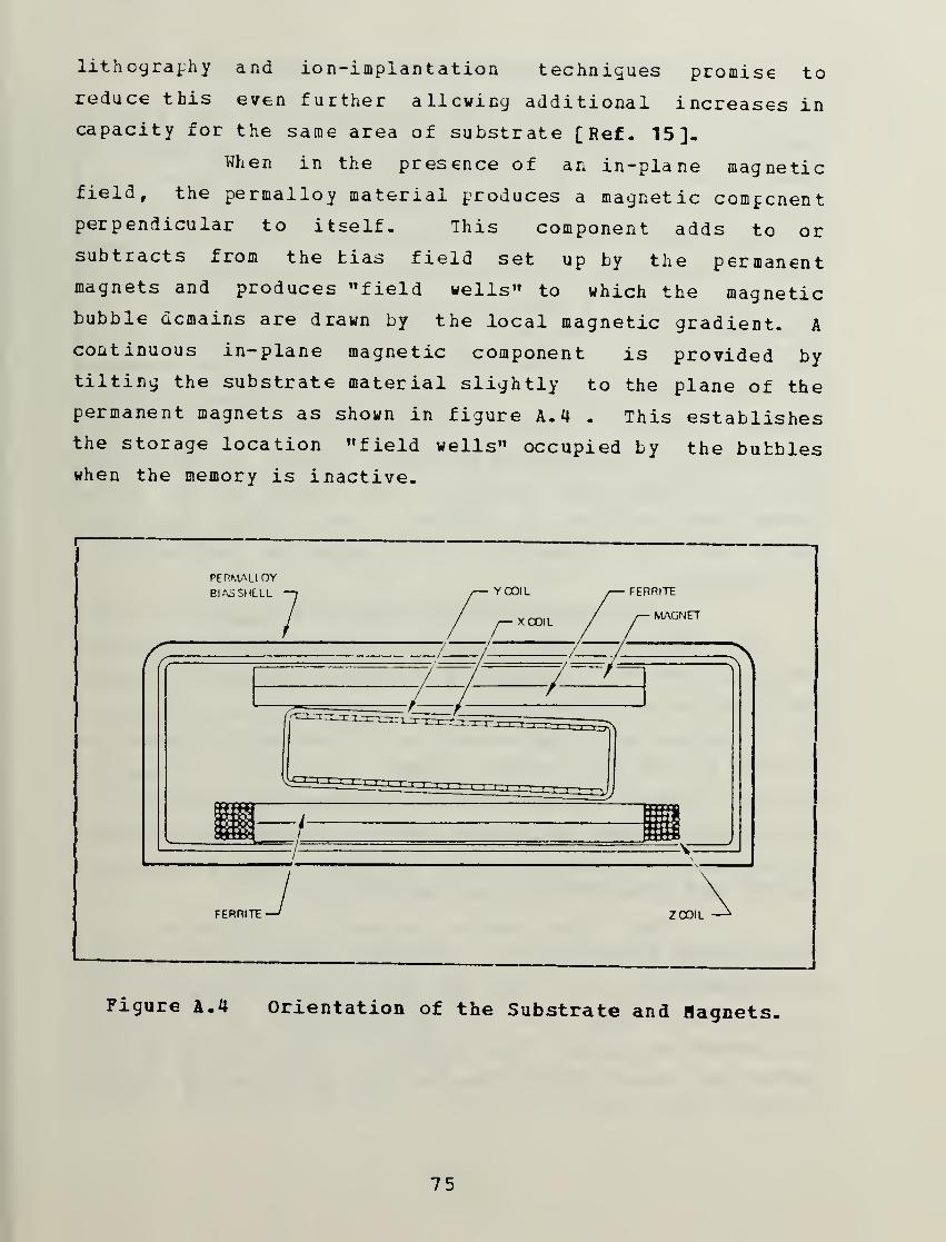
lithography and ion-implantation techniques promise to
reduce this even further allowing additional increases incapacity for the same area of substrate [Ref. 15].
When in the presence of an in-plane magneticfield, the permalloy material produces a magnetic componentperpendicular to itself. This component adds to orsubtracts from the bias field set up by the permanentmagnets and produces "field wells" to which the magneticbubble domains are drawn by the local magnetic gradient. A
continuous in-plane magnetic component is provided by
tilting the substrate material slightly to the plane of the
permanent magnets as shown in figure A. 4 . This establishesthe storage location "field wells" occupied by the bubbleswhen the memory is inactive.
PERMALLOYBIAS SHELL YCOIL
FERRITE
FERRITE
ZCOIL
Figure A. 4 Orientation of the Substrate and Hagnets.
75

b. Rotating Magnetic Field
For movement and accessability of the magnetic
bubbles, a rotating magnetic field is set up about the
magnetic substrate by two perpendicular coils driven at a
known frequency. See figure A. 4 and figure A. 13 at the end
of this section for coil configuration within the memory
cell. Sinusoidal currents oriented in quadrature through
the coils produce a smoothly rotating magnetic field. The
accepted method, however, is application of current pulses
through Schottky diodes which produce triangular waveforms
as shown in figure A. 5 . Application of current pulses is
easier to control digitally than application of sinusoidal
signals and the resulting waveforms produce an acceptablly
smooth rotating field vector. The timing of the pulses
establishes the rate of rotation of the field which deter-
mines the rate of movement of the magnetic bubbles within
the substrate.
The rotating magnetic field is oriented in-plane
to the substrate and produces a perpendicular magnetic
component from the permalloy structure as described earlier.
The rotation of the applied field combined with the shape of
the permalloy structure causes the "field well" beneath the
chevron to move in a known manner. The change in magnetic
gradient pulls a stored magnetic bubble along resulting in
controlled movement of bubbles within the material. Figure
A. 6 is used to explain bubble movement between structures
due tc an applied rotating magnetic field.
The first chevron in each row represents the
same chevron viewed at five different times while the field
is rotated about it. Each row shows three successive chev-
rons in what could be a line of associated data locations
within the substrate. The arrows to the right of each row
depict the rotating field vector set up at these discrete
76

11
V!
V?
Con nnv* i^cnniQi*
100 *H;
1? V
> 1
[ 1( 1 'h1
•,2 V
StaM. • fl.in- Siop-
'i c ,nesI i
II
180" ?70' 0" 90' 180" ?70r 0* 90" 180° ?70'
I
, C'o^pn i
i
Oi>*n
I
I
(»">#> r
r
Figure A -5 Rotating Magnetic Field Circuit and Waveforms.
times by the perpendicular coils- Denoting the first rcw as
having an applied vector of zero degrees, it can te seen
that a nubble exists in position 1 beneath the first two
chevrons and no data is stored in the third location. A
shift cf the rotating magnetic field vector by 90 degrees,
depicted in the second row, moves the "field well" beneath
77

ZP^ <£Pfc (P\a£^ ^
6^ £P% £R>3
o
£F*u ZP^ cCP^O 0- INPLANEUUIVEHELD
UIMEC1ION
Figure A. 6 Hovement of Bubbles Beneath a Permalloy StructureDae to a fiotating Magnetic Field.
each permalloy chevron to position 2 pulling the stored
magnetic bubbles along. Positions 3 and H show the bubble
positions during subsequent 90 degree shifts of the applied
field vector. Finally position 5 shows that after one
complete rotation of the applied field the "field well"
returns to its original position on the chevron. Butbles
that were at the end cf one chevron are drawn across the gap
to the "field well" of the next permalloy structure.
Bubbles are simply shifted linearly by one location each
complete cycle of the rotating magnetic field.
78

4 • L§L±& Storage Crganizat ion
Since movement of the magnetic bubbles withir the
substate is essentially serial between adjacent locations,
digital data could be stored ty placing the data into one
long loop of chevrons a single bit at a time as depicted in
Figure A. 7. This configuration has two major drawbacks.
First, a defect in a single chevron would break the conti-
nuity of the storage loop and the entire chip would be
useless. Secondly, retrieval of particular data would be
potentially slow since the desired data may need to be
rotated completely around the storage loop before arriving
at the output location.
Genera te
Detector
^
(a)
Replicate/transfer
I I
CJ
c
c
c
J
)
3
J
Figure A. 7 Single loop Bubble Storage Architecture.
Figure A. 8 shews the most accepted method of storing
magnetic bubble data known as the ma jor-track/minor-lcop
79

configuration. The major tracks are used for input and
output while the minci loops are used for data storage. The
method of introducing bubbles for storage and retrieving
bubbles as output data is discussed shortly.
Detector
?e ad trackV
D/ti\ s~\ sc\
• 1
1
Transferin V
Replicate/ fC\ /C\ f2\transfer
nor loons
V \a/ ^Y V j
r W r i t e track
e n e r a t e Annihilate vfv
Figure A. 8 Bajor/Hinor Loop Bubble Storage Architecture.
i
Each minor (storage) loop consists of many permalloy
chevrons configured in a single continuous path with the
input and output locations at opposite end of the loop as
shown. Bubbles are passed from the input track to a minor
loop and moved from storage location (chevron) to adjacent
storage location with each complete circuit of the rotating
magnetic field. Stored digital data continuously revolves
around the loop while the memory is active, or resides
motionless beneath a storage location chevron when the
80

rotating magnetic field is inactive. The major/minor loop
configuration makes each data bubble available at most after
one rotation of data through one of the smaller minor loops
plus the time to move the bubble along the output track.
For a fixed number of minor loops with a known number of
storage locations per loop, the access time of the system
can be determined from the frequency of the rotating
magnetic field.
Manufacture of the memory chip can include fabrica-
tion of a number of redundant storage loops onto the subs-
trate. This increases the yield of useable devices
containing a specified number of operable storage loops.
During testing, defective loops can be identified and a
"bootloop" code, representing the operational loops for that
specific chip, can be used during input and output processes
to ignore faulty or untested loops.
5 • Da ta Bubble Product ion
Eresence of a bubble within a magnetic bubble memory
is used to represent a "one" in digital data information.
Digital "zeros" are represented by the absence of a bubble
in a particular memory location. Data delivered to the
memory in digital form must be changed into a series of
magnetic bubbles suitable for storage. Since magnetic
bubbles can only exist within the substrate material, this
transformation must physically occur within the memory cell.
One method of bubble production is called nuclea-
tion. A current pulse is transmitted into a hairpin shaped
conductor beneath a permalloy structure which momentarily
creates a region of reversed magnetic potential to that of
the bias field. The resulting bubble is sustained by the
bias field and is available for propagation after the bubfcle
is stabilized. This process limits the rate of data input
due to the current pulse lengths required and time required
for the created domain to stabilize.
81

The accepted method for bubble production within a
bubble memory cell is through use of a "seed" bubble as
shown in figure A- 9. A permanently contained magnetic
bubble revolves with the rotating magnetic field within a
structure as shown. As the bubble passes over the conductor
strip it is elongated and cut by a short current pulse into
two bubbles, one which continues to rotate within the seed
bubble structure and one which is available for propagation.
For the cccurance of a "zero" bit, the bubble is simply not
split.
DIRECTIONOF CURRENT
PULSE
INPUTTRACK ~*
BUBBLESPLIT SEED
Figure A. 9 Bubble Generation for Input.
82

6. Eata Input
As described earlier, the major tracks in the major-
track/minor-loop storage architecture represent the paths
that magnetic bubbles follow when reading information in to
or out of the substrate. Figures A. 8 and A. 9 show the
bubble generator positioned at the beginning of the input
track. During an input operation the seed bubble is either
split or not split to produce a digital "one" or "zero" for
storage. Bubbles created are immediately streamed onto the
input track and propagate one location away from the gener-
ator each external field rotation making room for the next
data bit. As this implies, digital data delivered to the
memory must be configured serially for input. Additionally,
the data must be arranged in "pages" of streams of bubbles
and spaces having the same length as the number of available
minor storage loops configured on the substrate. When the
data have completely filled the input track, each bit of
data is positioned adjacent to a separate storage locp. The
entire page is transferred en mass to the minor loops in a
single "swap" operation as depicted in Figure A. 10. A
current pulse is applied through a conductor which causes
the bubble in the input track location to move onto the swap
gate location at the top of the storage loop and simultane-
ously moves the bubble previously in the swap gate to the
input track location. As a new page of data is streamed
onto the input track for storage, the old data bubbles
swapped from the storage loops are moved to an area at the
end of the input track known as a guard rail where they are
annihilated. It is important to note that as the data are
rotated about the substrate, data associated with a partic-
ular page maintain the same relative positions within the
storage loops as all bubbles move simultaneously.
83

INPUTTRACK
o c o .— KsH
'f\ <?J F"_-J \ coo
V \ f SWAP\J\ -v ,
} GATE (A)
Figure A. 10 Input of Data to a Storage Loop.
"7- I^ta Output
At the output side of a minor loop, data to be read
are reproduced from the output storage location by a "repli-
cate gate" as depicted in Figure A. 11. An applied current
pulse stretches and cuts the data bubble in much the same
way as in the seed butble operation, placing the new bubble
onto the output track while leaving the original bubble in
its storage location. Since the original data remain intact
and in original orientation within the memory, the read
operation is non-destructive. The replicate operation is
conducted simultaneously from all minor loops resulting in
retrieval of the page of data in the same serial pattern as
established during input of the information.
8 . Eutble Detection
The resulting stream cf bubbles and spaces repre-
senting the read data in page format on the output track is
fed serially through a voltage detection circuit which acts
on the magneto- resistive effect of its permalloy structure.
84

OUTPUTSTORAGE LOOP r\ r\ t-5.
TRACKX
' V 'A ' o
c »y^\5^.y—*^J^s)r)4
^Q° ° °^~^ a
K^ f -^r- G
. \U REPLICATEGATE (B)
Figure A. 11 Output of Data from a Storage Loop.
Presence of a bubble affects the resistivity of the struc-
ture as measured by an applied current. The data bubble is
first passed through a structure which enlarges the bubble
area to increase this effect. The detection circuit is
usually paralleled ty a dummy detector which provides
compensation for resistivity changes attributable to the
presence of the rotating magnetic field. Figure A. 12 is a
representative detection circuit. The microvolt output from
the detector representing the stored digital data must be
amplified to higher voltage level signals useable by
external devices.
9 . Data Orgjin iz ation and Addressing
Digital information is arranged in sequences of
pages for transfer and remains in page format while stored
in a bubble memory system. The dynamic nature of such a
system does not retain certain data in any discrete location
but does maintain the relative positions between pages by
rotating all bubbles around the storage loops simultane-
ously. External systems utilizing bubble memory must be
able to identify specific pages within the memory and
retrieve the desired page during a read operation. A
85

MAGNETORESISTIVEDETECTOR
OUTPUTTRACK
Figure A. 12 Magnetic Bubble Detection Circuit-
particular bit of information associated with a particular
page stored within the bubble memory cell must be derived
from the page after it is retrieved from the system. A
header/tail code could facilitate this process if necessary.
For use as a digital recorder, the starting and stopping
pages for particular information could be stored separately
to help identify specific recorded information.
10. Pernor y_ Cell Components
The term bubble memory "cell" is used to identify a
complete component capable of storing and transferring
magnetic bubble digital information. Figure A. 13 shows an
exploded view of the main components that make up an indi-
vidual memory cell. The entire package is usually contained
within a structure designed to minimize the effects of the
magnetic fields of the device on other memory components.
This alsc provides protection of the stored information from
86

external electro-magnetic interference or the radiations
which may be encountered in space.
SHIELD
PERMANENTMAGNET
COIL
BUBBLESUBSTRATE
PERMANENTMAGNET
Figure A. 13 An Exploded Yiea of a Memory Cell.
B. HEHOBT CELL REQOIBED SUPPOBT
Figure A. 13 describes the main components that make up a
memory cell capable of storing and transferring digital
information in the form of magnetic bubbles, however this
capability requires many of the processes to be initiated
and controlled externally. Figure B.10 is a block diagram
of a generic magnetic bubble memory system and identifies
the major functions provided to a bubble memory fcr proper
operation. Most of these functions were identified in the
87

description of the menory cell and the following subsections
address these functions in a general sense as a summary of
required memory cell support. Chapter 2 and appendix B
present the Intel Corp. components which perform these func-
tions specifically in the Intel-designed system.
a
Wll"" — ».
HO'.t
inte r taceD»t
1[
Coil flrivt1
1
write IV
bubble
devices
1
Syi tern
control an
J
timing
t<eOunGanc>
management
» — >
Sense 1
. >
Trarjf er
replicate
« ...
Figure A. 14 Hagnetic Babble Memory Required Systens.
1 Current Pulse Production
Current pulses are used by a number of components
within the cell. Bubble generation, replication, and swaps
require separate current pulses at precise times for proper
read and write operations and current pulses to the perpen-
dicular coils control bubble movement within the substrate.
88

Current must also be provided to the detection circuit in
order to measure tke magneto-resistive effect of bubble
presence during a read.
2- Input/Output Formatter
Digital data must be arranged into sequences of
pages for input to the bubble memory. Also, detected micro-
volt levels must be anplified and rearranged into the orig-
inal page format for output.
3 . C ontroller
Timing and control of the signals supplied to the
memory cell by the support components is the most critical
aspect cf magnetic bubble memory operation as described.
The write operation is a specific example. It must be
remembered that whenever the coils are activated, all
bubbles within the system move one location each complete
field rotation. Bubble generate pulses must be sent at the
precise time to arrange the bubbles in proper sequence on
the input track. The page of locations in which the infor-
mation is to be stored must be identified relative to the
other storage pages and the locations must arrive at the
swap gates at the same instant the bubbles on the input
track are aligned with their storage loops. The output
process is similar in timing requirements and signal
control.
Such a complex system requires a separate controller
component to coordinate the operation of the memory cell and
its associated support components and to provide an inter-
face to the external system utilizing the magnetic bubble
memory.
89

APPENDIX B
IHTEI CORP. HAGHETIC BOEBLE MEMORY COMPONENTS
This appendix describes the Intel Corp. components which
are the building blocks used to create the magnetic bubble
memory recorder systems described in this paper.
The appendix follows the format of Chapter 2 but pres-
ents the components in more detail including chip pin-out
signals and internal configurations, if applicable.
This thesis was initially based on the operation and
capabilities of components as described in the information
available in early 1S84. Since then, several anomalies have
been identified with the existing system.
Testing of the 7 114 MBM chips included identification of
enough storage loop pairs to produce the required 8192 to
meet design specifications. Pairs of loops were required
due to the fact that the bootloop code stored in each half
of the memory chip associated one bit with two storage
loops. This was necessitated by the limited space available
in the FSA bootloop registers. This bootloop coding scheme
limited chip production enough to convince Intel to consider
re-designing the system to allow a one-for-one coding by
increasing the available space within the registers.
An intermediate fix involving additional hardware was
developed by Intel and information describing these changes
was received early this year. The BPK 5V75A prototype kit
systems currently available incorporate an External Added
Redundancy Scheme (EARS) to act as an extended bootloop
register. An external EPROM, two FSAs, and a significant
amount of circuitry are required per bubble memory chip to
allow the one-for-one bootloop coding. Need for the addi-
tional hardware increases the complexity of the system as
90

well as the size and power consumption, adverse trends for
use in space-based systems attempting to minimize these
factors.
To resolve the anomalies, Intel Corp. is redesigning two
of the existing components and plans release of these chips
later this year. Specifically, a new 7225 bubble memory
controller chip will replace the 7224 BMC and a new 7245
formmatter/sense amplifier chip will replace the 7244 FSA
¥hich will alleviate the need for the additional hardware
and offer other benefits as well. These components have
been designed to integrate with the remaining original
elements of the system and the general descriptions given in
Chapter 2 apply egually to both generations of components.
However, due to the lack of specific information now avail-
able, component descriptions of this appendix do not include
the 7225 or 7245 chips. Instead, the existing 7224 BMC and
7244 ISA chips are described and differences expected from
use of the new chips mentioned. It must be pointed out that
the hardware interfaces associated with the new chips may be
slightly different than the existing components. System
schematics within this paper are based on the existing chips
and may require modification when the new chips are intro-
duced. However, the signals provided to the remaining system
elements must be the same as with use of the old chips so
the change may turn cut to be internal in nature and trans-
parent to the system designer.
A. TBE 7114 HAGMETIC BOBBLE MEMORY CHIP
Figure B. 1 identifies the 7114 magnetic bubble memory
(MBM) chip pin-outs ard associated signals. Table 10 gives
a short description of each of the pin-out signals identi-
fied in the figure including signal origin or destination.
91

rviLif com • inn• ipviCaTC |
1|
«f PVlCATt A I 1
•OOT MPJ
j
»oot s**» :—
I
m C r-—j
Gt «•! «»t«
I COILIKI • COiL i»
17
7114
WTI L MM-»fTIC J
• U=)0ETSUPPLYI»1- fTZJOETOUT a*• tTDOETOUTA-'• pnDETOUTB*- p3DET0UTB-
1
—
:s»ap a
P^T» COlLINr- cOil.in
2V|
r
Figure B.1 7114 Magnetic Babble Memory Chip Schematic.
The 71 14 magnetic bubble memory (M3M) chip contains the
substrate material in which magnetic bubbles are produced
and stored, the permalloy structures which determine bubble
location, the permanent magnets which ensure bubble
stability, and the perpendicular coils which control bubble
movement.
1 . Cata Storage Configuration
Figure B.2 shows the data storage configuration of
one half of the memory cell. Each half system is composed of
four "octants" of memory areas with permalloy structures
configured in the major-track/minor-loop storage architec-
ture. Each octant has its own seed bubble generator, input
track, and output track. Detector circuits are shared by
pairs of memory octants.
Each octant has 80 storage loops resulting in 640
total locps per chip. During the manufacturing process each
loop is tested and 540 perfectly operating loops are identi-
fied. Of these, 512 are used for data storage, 28 are used
to hold error correcting codes appended to the information
stored within the memory, and 2 contain bootloop information
92

TABLE 10
7114 HBB Fin-Out Signal Descriptions
SymDol Pin No | I/OI
SourceOesimalion Description
BOOT PEP 4 i 72 .14 iJpg T*o level current puise input tor reading me Doot
loop
BOOT bv'.AP E.l <\-34 CPU Singie-it-vei Curient pulse lor willing data inio tne
OOOt loop Th.s pin is normally usea on.y m memanufacture ot the MRM
Of r com .5 Giourj return tor tne Of lector tinace
OET OUT lb — 19 7244 FSA Diiterentidi pan iA A - ana B t B - i outpuis
wnich nave signals ol several miinvons pea*
ampiituop
DET SUPPLY 20 | 1 « 12 volt Suf. pry pin
GEN A ano OEN B 7, o l 7214 CPG Two ievpi current pulses lor Anting data onto tne
inoul trac>i
pulse com •
I 12 vOII SuDpiV C' ,n
HEP Adrj PEP B 3 2 i 7234 CPG Twoievei current pulses tor repiicai>ng oata trom
storage loops to output trac*
C.WAP A andS.VAPB
13 14 I 7234 CPG Single level current puise tor swapping oaia Worn
muut tracK to storaqe loops
X - COIL IN
X t COIL IN 9 10 I7 264 Terminals tor thp X or inner coil
V - COIL IN
Y « COIL IN 11 12 I 7204 Terminals tor tne Y or outer coil
J
identifying the useable loops. A single bootloop is used toidentify the operating loops within one half-system. Theremaining non-identified loops are either defective or notused and are masked ty the bootloop code. This redundant-loop manufacturing process increases the yield of useabledevices.
Each storage loop is made up of 8192 permalloystructures including the input and output locations. Thisresults in a single-chip user storage capacity of 4,194,304tits (four megabits) cf digital information.
93

oftcrom
a- t^£C
a—'
i
ill
i
1
a-
Pigure B.2 Intel 7114 Babble Memory Chip Data Organization.
2 • Cat a Input/O utp ut
In figure B.2 the left two octants are labelled
EARLY and the right two labelled LATE. Two bubble generate
signals are sent to each half of the memory chip each rota-
tion of the external rotating field, the presence of a
binary "one" to be represented by generation of a magnetic
bubble fcr storage with absence of a bubble representing a
binary zero. The first signal operates both bubble genera-
tors of the EARLY pair of octants creating two identical
streams of bubbles and spaces along the input tracks. The
second generate signal operates the LATE pair of generators
one half rotation of the external field later. Storage
loops, and their associated swap gates, are spaced every two
propagation locations along the input track. Data on the
input track of one of the pairs of octants is delayed by one
field rotation placing the odd bits at the swap gates of one
94

octant and the even bits at the swap gates of the ether
octant within a pair. A single current pulse swap signal
operates all swap gates in the memory simultaneously. The
duplicated bits on the input tracks not associated with a
swap gate, and the eld data tits swapped out of the memory
and onto the input tracks, propagate to the end of the input
tracks as new data is generated. The end of the track is a
"rail guard" where these unused bubbles are annihilated.
540 loops are used to store data within the bubble
memory chip. 512 hold information sent to the memory for
storage, and the remaining loops contain 28 bits of error
correcting code appended by an external device to every
block of data input fcr storage. Data must be arranged in
512 bit blocks ("pages") for each input operation and the
data streamed onto the input tracks properly to coincide
with the desired storage loop locations.
The output process is performed similarly. When the
desired data page is rotated under the replicate gate loca-
tions, a signal to the memory chip simultaneously reproduces
the data onto the output tracks of all the octants. Storage
loops are spaced every other location along the output
track, so the data of each pair of octants is merged
together to before being delivered to the shared detector
circuit. The magneto- resistive detector circuit voltage
signal is sensed by an external device which reconstructs
the original serial configuration of the data.
3 . Eootloop
Each half system in the memory chip contains a
storage loop dedicated to preserving the information which
identifies the operating storage loops in that half system,
and synchronization data used to determine the relative
position of the pages of stored information. This data is
loaded into the dedicated loop after the 540 operating loops
95

are identified during the manufacturing process. The infor-
mation is used by the support components in configuring the
data correctly for input and reading the data correctly
during output as well as Keeping track of the rotating data
pages.
B. TEE IHTEL 7250 COIL PRE-DRIVER CHIP AND 7264 COIL EBIVE
TBANSISTOHS
Using timing signals from the bubble memory controller,
the 7250 coil pre-driver (CPD) chip produces high current
outputs to the 7264 coil drive transistors (CDT) to form the
triangular waveforms which drive the perpendicular coils
around the 7114 MBM and establish the rotating magnetic
field for magnetic bubble movement within the cell.
1 7250 Coil Pre-Driver
Figure B.3 identifies the 7250 coil pre-driver (CPD)
chip pin-outs and associated signals. Table 11 gives a
short description of each of the pin-out signals identified
in the figure including signal origin or destination.
-
c§{ 1 16 "JVoo
rTsH C. 2 15 ~] xTouT
xT"in £ J 14 J X» OUT
x7\n C 4 7 132
]x OUl
v« in[
y^TnL
S
6i
,?
ii
J X OUT
;]y»out
Y- OUT C 7 10 1 Y4 OUT
GNC)[ B 9 M Y^OUT
•. _.
Figure B.3 7250 Coil Pre-Driver Chip Schematic.
96

TABLE 11
7250 CPD Pin-Out Signal Descriptions
Symbol Pin No I/O Source. Destination Description
i* j 1 l 7^44 FbA Cn.p seiecl li is active low v";nen nign crup is
aese'ectea ana 
12v 12v
nP
a - OUT
7250
pJ
CHAN
CPD
v+ OUT
f
NF"
CHAM
X+ OUT
7250
CPD
I. X- OUT
X- COIL IN X+ COIL IN
711^4 MBM
X COIL
Figure B. 4 7264 Coil Drive Transistor Schematic.
using timing signals from the bubble memory controller and
generate signals frcm the formatting device, the 7234
current pulse generator (CPG) sends current pulse signals to
the 7114 HBH which perform the generate, swap, replicate,
and bcotloop functions during read and write to the memory.
The 7234 also monitors both the 12 volt and 5 volt d.c.
supplies to the system and produces a power-fail signal to
the memory controller if either supply exceeds its threshold
values.
D. THE IHTEL 7244 FCEMATTER/SENSE AMPLIFIER CHIP
Figure B.6 identifies the 7244 formatter/sense amplifier
(FSA) chip pin-outs and associated signals. Table 14 gives
a short description cf each of the pin-out signals identi-
fied in the figure including origin or destination.
98

TABLE 12
7264 CDT Fin-Oat Signal Descriptions
7264
Four matched pair of N and P-channel tran-
sistors In industry standard TO 220 Discrete
packaging.
PIN 1 — GatePIN 2 & TAB — Drain
PIN 3 — Source
Symbol Pin No I/O Sou'ce destination Description
N Channel
GD
S
1
2
3
i
1
7250
71 14
G'Ound
Gate Drive Signal
Coil Orive Current
P Channel
G
D
S
t
2
3
1
1
7250
7114
G'Ound
Gate Drive Signal
Coil Dnve Current
Vf>p[ ii ]vcc
rs i[ i< i
f ah rin
?&!( r ] "(F 1
eiNfJic 7 11 Joins
CTs (Ki[i4
IS JCfN A
i*£f ni P ]S*A»
cJl If ] K|» B
sr^?N( i; )0|» *
¥o5f ?*{*[ 14 J »oor sw»»
§OOT In[ 10 t T J BOOT »IP
GSPf^ 1
1
1? JCNO
Figure B-5 7234 Current Pulse Generator Chip Schematic.
As the name implies, the 7244 formatter/sense amplifier
performs a number cf functions concerned in the data
transfer within the system. Figure B.7 shows a tlock
diagram of the internal configuration of the device.
99

TABLE 13
723Q CPG Pin-Oat Signal Descriptions
Symbol Pin No I/O Source Destination Description
BOOT EN 10 I 7224 BMC An active low input enabling tne BOOT REP output
Current pulse
BOOT HEP 13 7114 MBM An output providing the Current puise tor bootstrap
loop replication in tne DuDDie memory
BOOT SWAP 14 71 14 MBM An output providing a Current pulse whicn may be
ustd tor writing jata into the bootstrap loop
. 7224 BMC An active low input enabling the BOOT SWAP out-
put current pulse
BOOT SW EN 9 I
CS 7 I
7244 FSA An active low input tor selecting the chip The
cnip powers down during deselect
GEN A 18 71 14 MBM An output providing the current pulse tor writing
data into the A' Quads ot the bubble memory
GEN B 19 7114 MBM An output providing the current puise tor writing
data into the 8 quads ot the bubble memory
5 I 7244 FSA An active low input enabling the GEN A output
current pulse
GEN EN A
4 I 7244 FSA An active low mout enabling the GEN B output
Current pulse
GEN EN B
21 o 7224 BMC An active low open collector output indicating
that either v cc- or V Dn is below its threshold value
PWA FAIL
REFR 20 I External Resistor The pin tor the reference current generator to
which an external resistance must be connected
REP A 15 71 14 MBM An output providing the current puise tor replica
tion ot data in the A" quads of the bubble
memory
REP B 16 7114 MBM An output providing the current puise tor replica
tion ot data m the "B" quads ol tne bubble
memory
8 I7224 BMC An active low input enabling the REP A and REP B
outputs
REP EN
SWAP 17 7114 MBM An output providing the current puise tor exchang-
ing the data between the input track and the
storage loops in the bubble memory
SWAP EN 6 I
7224 BMC An active low input enabling the SWAP output.
TM A 2 I 7224 BMC An active low timing signal determining the cut
pulse widths ot the BOOT REP. GEN A, GEN B,
REP A and REP B outputs
3 I 7224 BMC An active low timing signal determining the
transler pulse widths ot the BOOT REP GEN A,
GEN B REP A and REP B outputs
TM B
The FSA is a dual-channeled device with one channel
corresponding to one of the half-systems of four octants in
the 7114 KBM storage scheme. The bootloop information is
100

m i ?o
ftlfCT OTjl [ i 11
c ec I li
{rb FTX5[ < 17
v n [ s 7
24
16
Of T »•[ 8 IS
on » [ J 4 M
DJ ' B' [ a 11
on * (i 1?
r.No [ 10 1 1
Jvci.
HflfC? IN
ICIK
J O'O
)Rf5fT
) Sniff CI*
]{N4fllf i
TfNi^if I
) 6a(» ouf I
) f3 S t » ou i i
Figure B.6 7244 Formatter/Sense Amp Chip Schenatic.
stored in a bootloop register to identify the operating
loops within the corresponding half-system. Each channel
also has a first-in/first-out (FIFO) register used in data
transfer to and from the bubble memory. Each FIFO holds 270
bits cf which 256 represent half of the 512 data bits per
page required for each transfer process. The remaining FIFO
spaces hold a 14-bit error correction code appended by the
FSA to each 256 bits of data input for storage to the
respective half-system.
The FSA also contains an internal status register which
is used to communicate the status of the FSA FIFO or infor-
mation concerning error correction capabilities or types of
detected errors.
The serial communications block serves as the interface
to the bubble memory controller. The DIO line is a
bi-directional serial bus which transfers data and commands
between the FSA and the controller. These functions are
differentiated by the signal level of the command/data (C/D)
line from the bubble memory controller. Commands are sent
to the FSA from the controller as one of the four bit words
described in table 15. These commands are sent to the FSA
automatically by the bubble memory controller to conduct the
operation requested by the external system. No direct inter-
action is required by the external system in sending the FSA
101

TABLE 14
72UU FS& Pin-Out Signal Descriptions
Symbol Pin No. I/O Source/Destination Description
CD 3 1 722* BMC Command-Data signal This signal snail cause the
FSA lo emer a receive command mode when high
and to interpret the serial data line as data wnenlow Any previously active command will be im-
mediately terminated by C D
CLK 18 1 CluCk Same TTL 'evei clOCK used ic generate internal
hming as used for D 7224-1
CS 1 1 External An act./e low signal used 'or multiplexing of
FSAs The FSA is disabled whenever CS is high
(i e it presents a high impedance to the bus andignores an bus activityl
QA'A OUT A
DATA OUT 3 11. 12 7234 CPG Output data from the FIFO to the MBM generatecircuitry Used to write data into ine bubble device
(active lowi
OETA-r DETA-DETB + DETB-
6 7 6 9 i 7114 MBM Differential signai lines irom the MBM detector
DiO 17 I/O 7224 BMC The Serial Bus data line ia bidirectional active high
Signal)
13 14 7234 CPG. 7250 TTL level outputs utilised as chip selects for other
interface circuits They shall be set and reset by
the Command Decoder under instruction of the
Controller lactive lowl
ENABlE A
ENABLE 5
EAR FuG 4 7224 BMC An error flag used to interrupt the Controller to in-
dicate that an error condition exists It shall be an
open drain active low signal
BESET 16 1 Power Fail Circuit An active low signal that snail reset ail flags andpomiers m the FSA as wen as disabimq the chip
as tre CS signal does Tne PESET pulse width
must be 5 ciock periods to assure the FSA is pro-
pe'iy reset
SELECT IN 19 1 7224 BMC An input utilised tor time division multiplexing Anactive low signal wnose presence indicates that
the FSA is to send or receive data from tne Serial
Bus during the next two ciock periods
SELECT OUT 2 o 7244 FSA The SELECT IN pulse delayed by two clocks II
shall be connected to the SELECT IN pin of tne
next FSA it is delayed bv two clocks because fhe
FSA is a dual channel device Channel A shall in-
ternally pass SELECT IN to Channel B (delayed by
one ciock)
15 1 7224 BMC A Controller generated clock signal tnat shall be
used to clock data out of the bubble I/O OutputLatch to the bubble module during a write opera-
tion and to cause bubble signals to be converted
by the Sense Amp and clocked into the Bubble I/O
Input Latch on a read
SHIFT CLK
commanc codes or any other of the bubble memory operating
control signals.
102

CO»T«c»
iN^ff^tAi :>'» «us a
tt<"100»
^A
A-
LAIOtS».M.» I O
CD-
wifrooi —fWAi —
DO —COMAOj^OrKJus
coumamo
| . ;«!»0U1 A% «IVf >1 ».
iniiwaCI ^itA,
.jSiFTCiBCl» Mil
in:i*aC( tssr_„J—- CaiaOuII
I o
r^
COVKTTXJAl -30 s~ v^
iNT(»N*. r ft! * * . t
Figure B.7 72U4 Fornatter/SeDse Aap Internal Block Diagram.
i
E. TEE FOOR-HEGABIT HEHOHY MODSJLE
The components described above are combined to form a
magnetic bubble memory "module" capable of storing up to
four-megatits of digital information. This module represents
the smallest building block component on which designs of
larger capacities and capabilities may be built.
103

TABLE 15
FSA Command Codes
NQME CODENo Operation 0000Reserved 0001Software Reset (3010Initialize 00 11Write MBM Data
(
O1O0Read MBM Data 0101Internally Corrected Data 0110Read Corrected Data 0111Ulrite &oot loop Register 1000Read Boot loop Register 1001Reserved 1010Reserved 1011Set Enable Bit 1100Read ERR. FLG/ Status 1101Set Correction Enable Bit 1110Read Status Reqister 1111
F. TEE "7221 COHTROLLEB
Figure B.8 identifies the 7224 magnetic bubble memory
controller (BMC) chip pin-outs and associated signals.
Tables 16 and 17 give a short description of each of the
pin-out signals identified in the figure including signal
origin or destination.
The 7224 contrcller is designed to coordinate the
efforts of the support components for proper operation of
the 7 114 MBM chip. The controller provides the support
chips with the timing signals critical for controlled move-
ment of the bubbles within the chip, proper creation and
sequencing of bubbles for input, and for timely production
of swap and replicate signals as required for data input and
output from the memory storage loops.
104

»»»»tll C ,
^~^*t 1 »tc
• till out I i m ] «cm 1
i >• ) »-
mill 14 II J »i
•o I 1 » ] »-
.• I < u ) lata
o»c« I 1 w J IK t
two i I 11 JIIMH
INI ( • IU4 " ) luilU
*.f 10 •"* II „J KM* IN
o. 11, 10 J *OOI (IN
0,1 II I* ) oo
0,1 ,1 u J on on
0,1 It » 1 iKHflA
0.1 II It ") Ml0. 1
It It ) tut HO
o, 1 II 1' J iM.ncii
0, 1 It 11 ] UNC0. 1 It 11 ) 0iO
OHO |
_________________10 li ] ci
Figure B.8 7224 Burble Memory Controller Chip Schematic.
The controller also serves as the interface between the
memory system and external systems utilizing the memory.
Based on ccramands received from the external system, the
bubble memory controller automatically generates the
required signals to the support components to conduct the
requested operation, with no further action required by the
external system other than to provide or accept data from
the memory system at a known rate.
A single bubble memory controller is designed to control
up to eiqht bubble memory chips simultaneously.
1 • 2224 BMC Internal Configurationi
The internal configuration of the bubble memory
controller is as shown in the block diagram of figure B.9.
The functions of the individual sections are briefly
described.
a. Sequencer
The execution and timing of memory operations is
coordinated through the sequencer.
105

TABLE 16
7224 BMC Pin-Out Signal Descriptions
Signal Name Pin No I/O Source Destination Description
v r- 40 i 5 VDCSupply
GND 20 I Ground
PWR FAiL 1 I 7214 CPG A lo* to'ces a controlled step sequence and hoids
BMC in an IDLE state isimiiar to RESET)
rTsTt out 2 725C CPD 7244 FSA72j4 RHe'enceCurrent Swit:n
An active low s.Giai to d/same external logic
initiated Dy PvVfl FAIL or RESET signals but not
active until a stopping point in a field rotation is
reacned (it tne BMC is causing the DuDDie
memory drive lieid to De rotated)
Clk 3 I Host Bus 2 MM.' TTL lever CIOCK
rTsTt 4 I host Bus A low on this pin forces the interruption ol any
BMC sequencer activity, performs a controlled
shutdown and initiates a reset sequence After
tne reset sequence is concluded a low on this pmcauses a low on the RESET OUT pm. furthermore,
the ne«t BMC sequencer command must De either
the Initialize or ADort command, all other
commands are ignored
RD 5 I Most Bus A low on this pin enaDies the BMC output data to
De transferred to the host data Dus (D?-Da)
WR 6 I Most Bus A low on this pm enaDies the contents of the host
data Dus (D D a ) to De transterred to the BMC
DACK 7 1 Most Bus A low signal is a DMA acknowledge Tnis
notifies the BMC that the next memory cycle is
available to transfer data This line should De
active only when DMA transfer is desired and the
DMA ENABLE bn has been set CS should not be
active during DMA transfers except to read status
it DMA is not used. CjaCR requires an external
puliup toVc C (5 IK onm)
ORQ 8 host Bus A high on this pin indicates tnat a data transfer
between tne BMC and the host memory is Deing
requested
INT 9 Most Bus A rismq eoge on this pm indicates tnat tne BMC has a
new status and requires serv cmg when enabled Dy
the host CPU
A 10 1 Most Bus A high on this pm selects the command/status
registers A low on this pm selects the data
register
Do-D7 11-18 I/O Most Bus host CPU data bus An eight bit bidirectional
port which can De read or written by using the
RD and WR stroDes D Shan be the LSB
D e 19 I/O Most Bus Parity bit
106

t. System Bus Interface
The system bus interface allows the bubble
memory controller to interact with an external system to
ensure transference cf data to and from the memory system at
the rate which is set by the number of memory modules teing
accessed simultaneously. The 7224 BMC is capable of
sustaining a transfer rate with an external system of up to
one-megabyte per second which is more than adequate for all
possible system operating configurations.
c. FSA Select Logic
Timing between the controller and the FSAs is
accomplished through this logic. Multi-memory module opera-
tion differs significantly frcm single module operation as
was described in Chapter 2.
d. Powerfail / Abort, Reset Logic
To preserve data integrity within the 71 14 MBM
the system must be shut down in a known manner. In the case
of a power failure or a commanded abort/reset, the shut-down
routine is activated by this section of the controller.
e. Register File
Six registers are accessed by the external
system to prepare the system for the up-coming operations.
The registers specify the operation to be conducted, the
amount of data to be transferred, the bubble cell to be
addressed, and the method to be used in the transfer. A
register is also used to report the status of the operation
and the occurance cf any errors or complications.
Operation of the bubble memory system requires
frequent interaction with the BMC registers as was described
in Chapter 3.
107

TABLE 17
7224 BHC Pin-Cut Signal Descriptions (cont.)
Signal Name Pin No I/O Source/Destination Description
CS 21 I Host Bus Chip Select Input A hign on this pm shall disable
the device to all but DMA transfers (ie.it ignores
bus activity and goes into a high impedance statei
DiO 22 10 T244 FsA A bidirectional active hign data line that shall be
used tor serial communications with 7244 FSAdevices
21 7244 FSA An active low output utilized to create time
division mu!tipie«mq slots in a 7244 FSA cnam It
shall also indicate the beginning ot d data or
command transfer between BMC and 7244 FSA
SYNC
24 /244 FSA A controller generated clocK tnat initiates data
transter between selected FSAs and their
corresponding bubble memory devices The timing
ot SHIFT ClK shall vary depending upon wnether
data is being read or written to the bubble
memory
SHIFT CLI\
25To IKef E«ternai
Circuit
An active low Signal that indicates that the DIO
line is m the output mode, i e BMC is sending
data to FSA It shall be used to allow ott board ex-
pansion ot 7244 FSA devices
BUS HD
26 i.O
To Alternate
Controiierisi
When user S,siemUbfS Mote Than
One Controller
A bidirectional pm that shall be tied to the WAITpin on other BMCs when operated in parallel It
shall indicate that an interrupt has been generated
and that the other BMCs snouid nalt in
Synchronisation with the interrupting BMC WAIT is
an open collector active low signal Requires an
external puiiup resistor to V <- (5 IK ohmi
WAIT
ERR FlG 27 1 7244 FSA An active low input generated external, oy
7244 FSA indicating that an error condition
exists it is an open collector input which requires
m external puiiuo resistor i5 IK onm)
2STo User External
Circuit
An active low signal that indicates the system is
m the read mode ana may be detecting It is useful
for power saving in the MBM
DETON
CD 29 7244 FSA A hign on this line indicates that the BMC is
beginning an FSA command sequence A low on
this line indicates that the BMC is beginning a
data transmit or receive sequence
BOOT SW EN 30 7234 CPG An active low Signji wnicn may be used tor
enabling the BOOT SWAP ot tne 7234 CPG
31 7234 CPG An active low signal used to create the swapfunction in external circuits
SWAP EN
32 7234 CPG An active low signal enabling the bootstrap loop
replicate lunction in external circuitry.
BOOT EN
REP EN 33 7234 CPG An active low signal used to enable the replicate
function in external circuitry
34 7234 CPG An active low timing signal generated by the
decoder logic tor determining TRANSFER pulse
width.
TM B
35 7234 CPG An active low timing signal generated by the
decoder logic for determining CUT pulse width
TM A
~. yT.X - , X
+
3639 7250 CPD Four active low timing signals generated by the
decoding logic and used to create coil drive
currents in the bubble memory device
108

«isrt —
WAlT -*—
Of T ON •»-
VCC
0| «-fte—
n —* n —
Back —Cs —
O»0 -m~
ml •»-
SlQulNCt"
8jS So •-
Cl«
FSAsuto
SVSTEMBUS
INTtflf ACSOAI A fit C'SUfi
DMA AhOINTI SHuPI
1OO1C
Figure B.9 7224 BMC Internal Configuration Block Diagrai.
f. FIFO
The FIFO is a 40 x 8 bits first- in/first-out RAM
used as a data buffer between the bubble memory and the
external system. Data is transferred between the BMC FIFO
and the ISA FIFO at a fixed rate which is multiplied by the
number of FSAs within the system. The average data transfer
rate to a single memciy module is 16 kbytes per second.
5 The FIFO in the 7225 bubble memory controller is to beincreased up to 124 x 8 bits. This equates to two fullsingle bubble memory pages. This improvement should makedata transfers easier to acccmplish and will protect thesystem from errors due to timing differences between thebubble memory and the external system better than the 7224BMC.
109

g. Signal Decoder / DIO
Signals to the bubble memory system must occur
at specific times in relation to the rotating magnetic field
which corresponds to bubble position within the memory. This
functional section of the controller contains the logic to
create these timing signals. This section also performs the
serial-tc-parallel and parallel-to-serial data conversions
required to communicate with the 7244 FSA over the serial
DIO line. Finally, this section also contains the logic to
encode/decode the bootloop information for use by the FSA.
Figure A. 14 is a circuit diagram of a complete
magnetic bubble memory system composed of the components
descrited above, capable of storing up to four-megabits of
digital information.
G. HDITIPIE HODOLE SISTEM COHFIGIIBATIONS
A single 7224 bubble memory controller is capable of
operating up to eight memory modules simultaneously. Figure
B.11 shows how the system as depicted in figure B.10 is
expanded to incorporate multiple magnetic bubble memory
modules.
The benefits of multiple module operations is presented
in Chapter 2 and will not be repeated here. However, the
method of communication between the bubble memory controller
and the multiple FSAs servicing their respective memory
modules is discussed in the next subsection.
1 . BMC - FSA Communications
Figure B.12 highlights the interconnections between
the BMC and multiple FSAs to help explain the method of
communication between the bubble memory controller and
multiple memory modules.
110

r -T.i5jSfi3 J
1t:j
—n § _ i 2 _.
<— ^— i—I
i——-J
. 1 5 5 1 4 -
131!in;1 3 2 *
-vnrr
I Mr!Ill
li
nil
'25:a*
h I
I
;
II
< i Tt ; i "•J
Win n
5£ -. ? r? -3 ni!« V ™ * V «'•
" i . i : • « II
lz±. - s
1 4
S- i
i i :
I;
i J i I
I 1
«:
Ul
r^\,!
ei c! » -i
i : !
- «4
i!
u,. _1I
I |T
m ei «j "# i
Z.iH1 ; " 3 ' r * S1 " T
lit I
?'<
[isSiiMsssssai
u*
i I
I
1* 4 *< 5 C -, 5 -' 5 c; -i ;,
.
i !i
i -
fi
«« \Aa a a a .-..i
I." I I rA, A .N A A N A S A
ILi_U
; S;i5JS3SXSiS3
XI
i
:
Figure B. 10 Four-Megabit System Circuit Diagram
111

»« •« i*-r.
£>.
Hh«r*.« • va
*Hh
;
OB T**,,d Tu-
-l-s-
r
t"'•
\
—
-
i—
.S
ItV Tlttf
a* i» n w
^
L
3TT « - T art our »-
t-
* **
• »
• t* i ••• *:* urn
«h-»o» • «***»
. i - . - -
..l*^** I
•OOf !•»»
-—
U
il -CO*.i»
CO*. «
-p- T 0f7 Owl .
idler own
Hire 3«f«0*1,1.' >M,'* »»II '•-»
Figure B. 11 fleaory System Expansion
112

7225
BMC
SYNC
command/data> "select in"
\V
DIO
r—A 2
a
5
PSA\V
MEMORY MODULE
t: 1
"select out"
xz "select in"
"'.a k/v«>»
Xa
5
s*
MEMORY MODULE
$ 2
"select out"
MEMORY MODULE
# 3 ETC.
Figure B.12 BMC - FSA Communications.
*
In order to share the same DIO serial communication
line between the BMC and the FSAs, communication must be
established with each FSA individually to avoid contention
over the single line- This is done by passing an enabling
signal from FSA to PSA via the chip "select in" and chip
"select out" lines. Commands and data sent over the single
DIO line are differentiated by the signal level on the
command/data line shared commonly by all FSAs in the system.
113

a. Establishing communication and commands
Figure B.13 is used to explain multiple module
accessing and command by the bubble memory controller.
» ClOC» MKOOl I . n ClOC« HHOM I. r» CtOC« M..OOI •
— JULnj^ulTJLT^T^^00 _
rU '
—
— u1_—' LSI •
^^
- _i:occcccco^x:co cccccccc ccccocI ....ti A K -"• D -i
|
it»toi «o>o [ o»r»ilMtl '
r~7«uri
""" *«TSi ' n« iitsi
aort. «T*rui n—o is Omlt miuht o» »u» »o» tni *l*o status COmmimo MOufmcl
J
Figure B.13 Access and Command of Multiple Memory Modules.
To establish communication, the BMC indicates
"command" by a high level signal on the command/data (C/D)
line, pulses the first FSA "select-in" line (SYNC as shown
in the figure) , and sends a 16-bit address word serially
over the DIO. Each pair of address bits corresponds to a
separate memory module FSA; the first two bits correspond to
the first FSA in sequence, the next two bits to the second
FSA, etc. The maximum number of FSAs and memory modules
that may be addressed by the bubble memory controller there-
fore is eight.
The first FSA delays the SYNC signal by two BMC
clock cycles and then repeats the pulse on its own chip
"select out" line which is connected to the following FSA
chip "select in" line. During these two clock cycles, the
FSA is enabled and looks for two high level pulses on the
DIO line. If the pulses are received, communication with
the module is requested and the FSA stands by to receive a
in

four-bit command when the C/D line is lowered indicating
data. If two "ones" are not received then that module is
not involved in the up-coming operation and remains on
standby. Elements within the standby module are not enabled
by the FSA and ignore timing and other signals from the BMC
on the other common lines.
The SYNC pulse is delayed two clock cycles
within each FSA before the signal is passed on to the next
sequential memory module. The C/D line is held high for 20
clock cycles no matter how many modules are in the system or
how many modules are to be addressed. 20 additional clock
cycles are allocated after the C/D line is lowered for the
BMC to send out the four-bit command code and, if the
command is to check the FSA status (only one module can be
addressed at a time for this operation) , to receive the
eight-tit status word from the addressed FSA. It is after
this point that data may be transferred between the BMC and
FSAs in the method described next.
Note that the four-bit command codes sent by the
BMC over the DIO are read simultaneously by all enabled FSAs
when the C/D line is lowered. This indicates that all
enabled modules perform the same functions when operating in
parallel.
O) Multiple Module Data Transfers. Figure
B.14 depicts the timing involved when the received ccmmand
from the BMC calls fcr data transfers. The SYNC pulse on
the first FSA chip "select in" line enables it to access the
DIO line. Since this signal is delayed two BMC clock
cycles, only two bits of data are transferred with a single
module each BMC SYNC pulse. The SYNC pulse is daisy-chained
down the line of FSAs and the BMC correlates bits in
sequence on the DIO line to the enabled FSAs. A new SYNC
pulse is sent out by the BMC every 20 clock cycles until at
least one "page" of data has been transferred between the
115

EMC and each FSA invclved in the operation. This set timing
scheme establishes the data transfer rates and required page
sizes associated with different memory module accessing
configurations.
--•TjinjmjTJUiiiiiiiiiniTj^^
"U LT^-nZCCDOJZCQOOOOOn oc
STsc"
010
DATA TO 111 FSA J.
DATA TO thFSA —DATA TO ihFSA
'30CLOCK PULSES BET*EEH SYNC PULSES
Figure B.14 Bultiple Hodule Data Transfers.
H. OPERATING LIMITATIONS AND REQUIREMENTS
This section will outline the operating limitations of
the Lubble memory system and describe some of the system
requirements includirg recommended support circuits.
1 . Operat ing Limitations
Table 18 lists some of the operating limitations of
the 7114 magnetic buttle memory chip.
2- ffoltage Regulator Circuitry,
Figure B.15 depicts a voltage regulation circuit
used by Intel on the BPK prototype kit. Intel recommends
that multi-module configurations, such as described in
116

TABLE 18
7114 Absolute Maximum Ratings
Operating Temperature 10*C to 55*C CaseRelative Humidity 95°o
Shell Storage Temperature (Data Iniegntv
Not Guaranteed). . .- 55°C to + 125*C 'COMMENT Stressesaoove thosehsted under "Absolute
Voltage Applied to DET. SUPPLY 1 4 v/ous Maximum Ratings may cause permanent damage to meVoltage Applied to PULSE COM 14 volts device Tnis is a stress rating oniy and functional opera-
Continuous Current between DET COM and tion of me device at tnese or any other conditions acoveDetector Outputs 20 mA r^ose indicated m me ooe rat:onai sections o> tn*s
Coil Current 5A D C. speculation is not implied Exposure to aDsoiute man-External Magnetic Field tor mum rating conditions tor extenaed periods may atiect
Nonvolatile Storage 20 Oersteds oewce renaoiiity
Non-Operating Handling Shock(without socket) 200G
Operating Vibration (2 Hz to 2 kHzwith socket) 20G
Chapter 2, should include one voltage regulation circuit per
memory beard. The regulator circuit is intended to maintain
the vcltage supplies within tolerated limits which are +5V
PC (/- 5%) and +12V DC (+/- 13)-
3 • Powerf ail C ircu it
Figure B.11 depicted a powerfail circuit associated
with the bubble memory system. The circuit is designed to
detect if either of the reguired power sources fall beneath
the low-end margins for operation (-5% on the 5V supply and
-1% on the 12V supply). The circuit assists the 7234 CPG
which provides the pcwerfail signal to the bubble memory
contrcller to shut down the system in a manner which
preserves data integrity.
The circuit also contains storage elements to main-
tain adeguate power for proper system shut-down, and a
powerfail signal delay circuit to prevent powerfail indica-
tions during system pcwer-up.
117

. t|* t * ^- 1..
* f • »-vw—
TH
—
I
:
•«>
LI.
. -i .* * i -
Figure B.15 Voltage Regulator Circuit.
I. TEE EPK 5V75A PROTOTYPE KIT
Figure E.16 depicts the BPK 5V75A four-megabit magnetic
bubble memory prototype kit presently available from Intel.
The kit is basically a single memory module with a dedicated
7224 tulble memory controller chip and necessary support
circuits. The major components and circuits are annotated on
the figure. Of particular interest are the voltage regulator
and powerfail circuits, dual 7245 formatter/sense ampli-
fiers, and external EEROM. The dual FSAs and EPEOM are part
of the External Added Redundancy Scheme (EARS) modification
Intel has incorporated to increase the production yield of
useable devices.
118

Figure B. 16 BPK 5V75A Prototype Kit
119

LIST OF REFERENCES
1. NASA Contractor Report 3380, Bubble Memory Module, byO.D. Bohning and F.J. Becker, Eecember l y bO
«~
2- Options "White Paper" On Mass Storage Devices.Preliminary ITeport obFainecPfrom NASA GocTdard, "Parch1985
3. Camtou, B., Challeton, D., Mauduit, D. , "The Influenceof Neutron and Gamma Irradiation in Bubble GarnetFilms," IEEE Transactions on Magnetics, v. mag-17, n.2, pp! 25F5=25F77~ffovem~5€r~T9HT7
4. NOAA Technical Memorandum NESS 95, The Tiros-N/NOAAk'G Satellite Series, by A. Schwa lb, March T978.
5. NASA Contract Report NAS2-10380, Titan ProbeTechnology. Assessment and Technology Developmen tTIanSTuo'y, By A. 71. Carro, July 79UU.
6. Hoagland, A. , "Storage Technology: Capabilities andLimitations," Compute r v. 12, n. b, May 1979.
7. Newman, P., "Magnetic Bubble Memories: Part 3 TheMarket and Potential Suppliers," Elec t ronicEngineering, pp. 43-58, September 1979.
8. Bryson, D.f
Clover, D., Lee, D., "Megabit BubbleMemory Chip Gets Support from LSI Family,"Electronics, 2 6 April 19 69.
9. Washburn. H. , Nicolino, S., "Bubble Chip Packs 4 Mbitsinto 1-Mbit Space," Electronic Design, pp. 111-117, 11November 1982.
Hill, R., Aircrew Modularized Inflight DataAcguisition S ystem , Ma"sterT s THesis, Air ForceInstitute of Technology, December 19 78.
11. Intel Application Note AP-187, Megabits to Megabytes:B ubble Memory System Design and Boar3 layout, '"by S.Knapp, tJecember i"9Btf.
12. Intel Publication No. 2444-001, BPK 5V75A Four-megabitBubble Memory Prototyping Kit UserTs ManualT T9BT-
13. Lammer, P., "On/Off Scheme Slashes Bubble Memory'sPower Drain," Electronic Design, pp. 231-234, 22 March19 84.
120

14. Markham, D., "Magnetic Bubble Memories: Part 1 TheDevice," Elect ronic Engineering, pp. 85-99, June 1979.
15. Triplet, B. , Jones. S., "X-Ray Lithography,"Proceedings or the International Society of OpticalEngineering v7 23T7 pp7~TTB::T237~1 9HZ"!
121

BIBLIOGRAPHY
Altman, L. , "New Arrivals in the Bulk Storage Inventory,"Electronics, v. 51, n. 8, 13 April 1978.
Eecker, F. , Murray, G. , BohEing, 0., Stermer, R., "An8x10**5 Bit Bubble Memory Cell for Spacecraft Applications,"IEEE Transacti ons on Magnetics, v. mag- 16, n. 5, September
Bohning, 0., Adler, S. , Nichols, C, "A Bubble DetectionCircuit for Spacecraft Applications," IEEE Transacti ons onMagnetics, v. mag-16, n. 5, September 1UBT3.
Eryson, C. , Lee, D. . "LSI Support Circuits Take the TroubleOut of Designing Bubble-Memory Systems," Electronic Design,v. 27, n. 24, 22 November 1979.
Hayes, P., Segura, R., Stermer, R., Bohning, 0., "A EubbleMemory Module, " IEEE Transactions on Magnetics , v. mag-16,n. 5, September T9HTJ.
Hunter, E. , "Magnetic Bubble Memories: Systems," Elect roni cEngineerin g, July 1979.
Robertson. B. , "California Hardware," Byte, v. 8, n. 11,November 1983.
Sando, S., "Performance of One Megabyte Bubble MemorySystem," I EEE Computer Society International C onfe rence,Spring, 19BU7
-
Scharrenterg, B., "The Ins and Outs of NonvolatileSemiconductor Memories," Electronic Design, v. 31, n. 17,August 1983.
Siegel, P., "Megabit Bubble Memory for Non-volatileStorage," E lectronic Eng inee ring, v. 52, n. 634, February1980.
Thorp, A., "New Bubble-Memory Packaging Cuts Board Space andManufacturing Costs," Electronics, v. 56, n. 6, 24 March1983.
122

INITIAL DISTRIBUTION LIST
No. Copies
1. library. Code 142 2Naval postgraduate SchoolMonterey, California 93943
2. Defense Technical Information Center 2Cameron StationAlexandria, Virginia 22304-6145
3. Chief of Naval Operations 1
Department of the Navy (OP-943E)Washington, D.C. 20350
4. Commander 1
Naval Electronic Systems CommandNaval Electronic Systems Command HeadquartersWashington, D.C. 20370
5. Ccmmander 1
Naval Space CommandDahlgren, Virginia 22448
€. Commanding Officer 1
Kaval Research laboratoryWashington, D-C. 20375
7. Professor Rudolph Panholzer. Code 62 5Department of Electrical ana Computer Engineering,Naval Postgraduate SchoolMonterey, California 93943
8. Professor Robert Strum, Code 62 1
Department of Electrical and Computer Engineering,Naval Postgraduate SchoolMonterey, California 93943
9. It. Bruce A. Campbell 3Aerospace Engineering Dept. (11B)U.S. Naval AcademyAnnapolis, Maryland 21402-5042
123

/ /*?


211*102
CampbellA digital recording
system for space-basedapplications utilizingfour-megabit magneticbubble memories.
ThesisCI 9326c.l
2IM02Campbell
A digital recordingsystem for space-bas3dapplications utilizingfour-megabit magneticbubble memories.
> 81N0fO
