a dissertation submitted in partial satisfaction of the … · 2018-10-10 · understanding...
TRANSCRIPT
Understanding Magnetism in Multiferroics
by
Mikel Barry Holcomb
B.S. (Vanderbilt University) 2004
M.S. (University of California, Berkeley) 2006
A dissertation submitted in partial satisfaction of the
requirements for the degree of
Doctor of Philosophy
in
Physics
in the
Graduate Division
of the
University of California, Berkeley
Committee in charge:
Professor R. Ramesh, Chair
Professor Joel Moore
Professor Yuri Suzuki
Fall 2009

The dissertation of Mikel Barry Holcomb is approved:
Chair ______________________________________________ Date: ____________
Professor R. Ramesh
______________________________________________ Date: ____________
Professor Joel Moore
______________________________________________ Date: ____________
Professor Yuri Suzuki
University of California, Berkeley
Fall 2009

Understanding Magnetism in Multiferroics
© 2009
by Mikel Barry Holcomb

1
Abstract
Understanding Magnetism in Multiferroics
by
Mikel Barry Holcomb
Doctor of Philosophy in Physics
University of California, Berkeley
Professor R. Ramesh, Chair
This dissertation details the study of electric and strain control of
antiferromagnetism and ferromagnetism at room temperature using multiferroic BiFeO3
thin films. Piezoelectric force microscopy and photoemission electron micrscopy
techniques were used to correlate ferroelectric and antiferromagnetic domains. An angle-
dependent dichroism intensity formula was established and applied to determine
magnetic behavior. The effects of thickness and orientation on ferroelectric and magnetic
properties in BiFeO3 films were studied. These results were used in the making of a
magnetoelectric-ferromagnet heterostructure in which electrically assisted exchange bias
was observed. This toolbox of control parameters gives a very strong benefit for the
making of new and improved devices, particularly in the computing industry where the
traditional magnetic field controlled devices are reaching their limits.
Chair ______________________________________________ Date: ____________
Professor R. Ramesh

i
DEDICATIONS
There are a great number of people who have developed me into the scientist and teacher
that I am today. I dedicate this dissertation to you. Let me point out a few of these people
for whom I am particularly grateful.
I would like to thank my advisor Professor Ramesh whose never-ending passion for
science has kept me motivated and encouraged me to push my limits.
I am grateful for the effort of many beamline scientists (Andreas Scholl, Jeff Kortright,
Andrew Doran, Elke Arenholz, Arantxa Fraile-Rodriquez) whose expertise in their
equipment and research field has allowed me the ability to quickly attain and analyze new
experimental procedures. Andreas’ tireless answering of so many of my questions has
allowed exciting new science to take place.
I would like to thank so many teachers from high school (Henry County, Kentucky),
undergraduate (Vanderbilt University), and graduate school for encouraging me to reach
for the stars. Without your constant support, I may never have gained the self confidence
that allows me progress in this fascinating field. Let me specifically thank Professor
Sheldon (Vanderbilt) who encouraged my interest in undergraduate research by setting
up interviews with the local professors. I was able to interview the professors and find out
what research was right for me. I am very happy with my choice.

ii
This leads me to thank my undergraduate advisor Professor Tolk. I appreciate his effort
to fill in the background when others might say I was not yet ready for research due to
still being too young. I am thankful for the experience he allowed me not only in the
laboratory, but also dealing with grant writing and teaching. Also, there was nothing
better than a party at the Tolk’s house.
Another “teacher” I would like to thank is my mother. She taught me that I can do
anything to which I put my mind. I appreciate her help in making my education possible
even when it seemed above our means. She has always been available to me any time I
have an issue which I seek her advice.
My husband should not be so far down on the list of people I would like to thank. He has
allowed me not to go insane with his willingness to take care of a great deal of little
things that pile up. He also has been gracious enough to let me practice important talks on
him and to edit many of my writings. His help has allowed me to be much more efficient.
He has also kept me very happy.
I would like to thank so many of my friends such as Seth, Steve-Steve, Dave R., Dave P.,
Joel, Allen, and Sarah for helping me learn how to talk to scientists not in my field and
giving me much needed relaxation.
I am thankful to have had intriguing discussions with many scientists about my project
and the future of the field. A few professors and scientists have gone out of their way to

iii
have continued debate include Nicola Spaldin (UCSB), Joe Orenstein (UCB), Jo Stohr
(Stanford), Jeff Kortright (ALS), and Robert Shelby (IBM Almaden).
There are many others that will go unnamed. Thank you for all of your support and
guidance.

iv
TABLE OF CONTENTS
LIST OF FIGURES……………………………………………………………….. viii-xiii
LIST OF SYMBOLS & ABBREVIATIONS………………………………………. ix-xvi
ACKNOWLEDGEMENTS……………………………………………………... xvii-xviii
CHAPTER 1 – Complex Oxides and Their Complex Behavior…………………………. 1
1.1 – Complex Oxides………………………………………………………………... 2
1.2 – Controlling Order Parameters………………………………………………….. 3
1.2.1 – Ferroelectricity…………………………………………………………… 3
1.2.2 – Magnetism………………………………………………………………... 5
1.2.3 – Multiferroics and Magnetoelectrics……………………………………… 7
1.3 – Understanding and Controlling Magnetism…………………………………... 10
CHAPTER 2 – The Technique Behind Probing Magnetism—X-ray Absorption……… 11
2.1 – Synchrotron Radiation History……………………………………………….. 12
2.2 – Polarized X-rays………………………………………………………………. 13
2.3 – Experimental Techniques……………………………………………………... 14
2.3.1 – X-ray Absorption Spectroscopy………………………………………… 14
2.3.2 – Total Electron Yield…………………………………………………….. 15
2.3.3 – Photoemission Electron microscopy……………………………………. 16
2.4 – X-ray Absorption Line Shape………………………………………………… 18
2.4.1 – The Golden Rule and Selection Rules………………………………….. 18
2.4.2 – Elemental Specificity…………………………………………………… 19

v
2.4.3 – X-ray Magnetic Circular Dichroism……………………………………. 21
2.4.4 – X-ray Magnetic Linear Dichroism……………………………………… 23
2.4.5 – Combining XMCD and XMLD………………………………………… 26
CHAPTER 3 – Electric Control of Antiferromagnetism……………………………….. 31
3.1 – Theory of Electric Control of Magnetism in BFO……………………………. 32
3.2 – Ferroelectric Switching of BFO………………………………………………. 33
3.3 – Angular Dependence………………………………………………………….. 34
3.4 – Ferroelectric Contrast in PEEM………………………………………………. 35
3.5 – Temperature Dependence…………………………………………………….. 36
3.6 – Magnetoelectric Coupling…………………………………………………….. 39
3.7 – Confirmation………...………………………………………………………... 42
CHAPTER 4 – Thickness Dependence of Magnetism in BFO………………………… 44
4.1 – Bulk BFO……………………………………………………………………... 45
4.2 – BFO Thin Films………………………………………………………………. 47
4.2.1 – Discovering Differences Between Thin and Thick Films………………. 47
4.2.2 – Exploring Reasons for Differences……………………………………... 49
4.2.3 – Angle-Dependent Measurements of BFO Thin Films………………….. 54
4.2.4 – Modeling Expected Domain Contrast………………………………….. 57
4.3 – BFO Ultrathin Films………………………………………………………….. 65
4.4 – Summary of BFO Thickness Effects...……………………………………….. 67

vi
CHAPTER 5 – Orientation Influences on Magnetic Order…………………………….. 69
5.1 – Comparison of Ferroelectricity in BFO Orientations………………………… 70
5.2 – Magnetism in 110 BFO films……….………………………………………... 71
5.3 – Magnetism in 111 BFO films….………..………………………………….… 80
5.4 – Summary of Orientations……………………………………………………... 82
CHAPTER 6 – Electric Control of Exchange Bias…………………………………….. 83
6.1 – Exchange Bias Background…………………………………………………... 84
6.2 – Interface Control……………………………………………………………… 86
6.3 – Domain coupling between magnetoelectric BFO and ferromagnet CoFe……. 88
6.4 – Horizontal Poling of BFO Domains………………………………………….. 90
6.5 – Electric Field Control of CoFe Ferromagnetism……………………………... 92
CHAPTER 7 – Summary of Results and Future Directions……………………………. 95
7.1 – Introduction…………………………………………………………………… 95
7.2 – Techniques for Measurement…………………………………………………. 96
7.3 – Electric Control of Antiferromagnetism in BFO…………………………...… 96
7.4 – Thickness Effect on Properties of BFO………………………………….…… 97
7.5 – Orientation Effects on the Ferroelectric and Magnetic Properties of BFO…... 98
7.6 – Exchange Bias with BFO…………………………………………………….. 99
7.7 – Overall Summary……………………………………………………………. 100
APPENDIX A – Growth of Epitaxial BFO Thin Films………………………………. 101
vii
APPENDIX B – Piezoelectric Force Microscopy…………………………………….. 102
REFERENCES………………………………………………………………………... 104
viii
LIST OF FIGURES
Figure 1: Perovskite structure and variety of properties……………………………..… 2
Figure 2: Electric field dependence for a) dielectric and b) ferroelectric materials……. 4
Figure 3: Rhombohedral structure of BFO at room temperature…………………….... 4
Figure 4: In-plane PFM image of BFO thin film………………………………………. 5
Figure 5: Magnetic order in BFO with respect to the [111] ferroelectric direction……. 6
Figure 6: Correlation of ferroelectric and magnetic ordering………………………….. 8
Figure 7: Total electron yield description. a)-c) illustrate the excitation and decay of
electrons in TEY. d) One x-ray creates several secondary electrons within the
sampling depth L. e) These secondary electrons dominate the TEY
intensity........................................................................................................... 15
Figure 8: Electron-optics of PEEM2 at the ALS……………………………………… 16
Figure 9: Beamline setup at 7.3.1 at ALS…………………………………………….. 17
Figure 10: Plot of total electron yield for wedge Cu/Fe/Ni sample……………………. 19
Figure 11: L-edge x-ray absorption edge spectra………………………………………. 20
Figure 12: Typical Fe XAS and XMCD……………………………………………….. 21
Figure 13: Origin of spin and orbital moment sensitivity……………………………… 21
Figure 14: L2 linear Ni edge……………………………………………………………. 23
Figure 15: Contrast vs azimuthal angle………………………………………………… 23
Figure 16: XMLD image B/A………………………………………………………….. 24
Figure 17: NiO AFM contrast temperature dependence from Ni L2-edge fine structure
with superimposed theory curves…………………………………………… 25
Figure 18: L edges of Ni and Co for sample and metal and expected oxidation state…. 26
Figure 19: XMCD of Co (top) and Ni (middle) and XMLD of NiO (bottom) with 45°
rotation……………………………………………………………………… 27

ix
Figure 20: XMCD, interface thickness, and coercivity……………………………..….. 28
Figure 21: Schematic diagram of (001)-oriented BiFeO3 crystal structure and the
ferroelectric polarization (bold arrows) and antiferromagnetic plane (shaded
planes). a) Polarization with an up out-of-plane component before electrical
poling. b) 180◦ polarization switching mechanism with the out-of-plane
component switched down by an external electrical field. The
antiferromagnetic plane does not change with the 180◦ ferroelectric
polarization switching. 109◦ (c) and 71◦ (d) polarization switching
mechanisms, with the out-of-plane component switched down by an external
electrical field. The antiferromagnetic plane changes from the orange plane to
the green and blue planes on 109◦ and 71◦ polarization switching
respectively…………………………………………………………………. 32
Figure 22: Out-of-plane (a) and in-plane (b) PFM images of the as-grown BFO film. Out-
of-plane (c) and in-plane (d) PFM images taken after applying an electric field
perpendicular to the film on the same area as in a and b. Different polarization
switching mechanisms are described in the table…………………………... 33
Figure 23: In-plane PFM images before (a) and after (c) 90◦ in-plane rotation. The arrows
show the direction of the in-plane component of ferroelectric polarization.
PEEM images before (c) and after (d) 90◦ in-plane rotation between the two
images. The arrows show the direction of x-ray polarization relative to the
domain structure…………………………………………………………….. 34
Figure 24: (a) PEEM, (b) AFM and (c) PFM images of PPLN. The fields of view are 40
µm. Insets in (b) and (c) are 10x10 mm2 and obtained from the same surface.
In (b), the double lines remained at the negative domain boundary regions
after the lithography process. In (c), the PFM image obtained from the same
region of the AFM image shows that the marked regions are negative domains
which are brighter and wider than the positive domains…………………… 35
Figure 25: Temperature dependence of normalized order parameters of BiFeO3. The
linear dichroism, out-of-plane lattice parameter and ferroelectric polarization
are normalized to the values at room temperature; the Bi and Fe atom
displacements and <M 2> are normalized to the values at 0 K……………... 36
Figure 26: PEEM images before (a) and after (b) poling. The arrows show the x-ray
polarization direction. In-plane PFM images before (c) and after (d) poling.
The arrows show the direction of the in-plane component of ferroelectric
polarization. Regions 1 and 2 correspond to 109◦ ferroelectric switching,
whereas 3 and 4 correspond to 71◦ and 180◦ switching, respectively. (e) A
superposition of in-plane PFM scans shown in c and d used to identify the
different switching………………………………………………………….. 38

x
Figure 27: Table of Bragg intensities for BFO crystal before (top) and after (bottom)
electric field poling…………………………………………………………. 42
Figure 28: (a) Schematic of spiraling of the antiferromagnetic order in BFO. (b) Neutron
intensity around the (½, -½, ½) Bragg reflection…………………………… 45
Figure 29: PEEM image of BFO crystal reveals large FE stripes with magnetic
variation…………………………………………………………………….. 45
Figure 30: (a) PEEM image showing the location of three areas for x-ray light polarized
at α= 0°. (b) The angular contrast of these areas are shown through the light
polarization rotation………………………………………………………… 46
Figure 31: Recent understanding of ferroelectric hysteresis curves for 200 nm thick BFO
films and crystals…………………………………………………………… 48
Figure 32: Film thickness dependence of (a) c-axis lattice parameter, (b) spontaneous
polarization P0, and (c) saturation magnetization Msat with the saturated
magnetic field of 6000 Oe…………………………………………………... 49
Figure 33: (a) XRD θ-2θ scans for the BFO films of varying thickness on STO substrates
and (b) out-of-plane lattice parameter as a function of thickness on STO and
DSO substrates……………………………………………………………….50
Figure 34: Schematic showing six energetically preferred axes for BFO with ferroelectric
polarization (FE) pointing along [111]……………………………………... 51
Figure 35: The crystal structure of thin and thick BFO films grown on SRO/STO(001).
RSMs for thin (a) and thick (b) BFO grown on SRO/STO(001). (c) Schematic
illustrating the nature of the crystal structure of the BFO film, where a is the
in-plane lattice parameter, c is the out-of-plane lattice parameter, and β is the
monoclinic distortion angle. (d) Unit cell parameters, as determined by RSM,
for both strained (thin) and relaxed (thick) films…………………………… 52
Figure 36: PFM image of in-plane polarization projections with PFM and PEEM
geometries (taken separately), showing incident x-rays 30 degrees from
sample surface………………………………………………………………. 54
Figure 37: PEEM images of BFO at several angles of the electric vector of incident linear
polarization α. (a) Schematic illustrating the experimental geometries used to
probe the angle dependent linear dichroism in BFO. The outlined arrows show
the in-plane projection of the four ferroelectric directions. Images of domain
structures taken at (b) α=90°, (c) α=70°, (d) α=40°, and (e) α=0°………….. 55
Figure 38: PFM and x-ray measurements of ferroelectric domains on PZT. In the same
location, we present (a) the out-of-plane and (b) in-plane projections of the
ferroelectric directions, and (c) the PEEM dichroic contrast taken at the Ti L2-
xi
edge. (d) The angular dependence of L2B/L2A as the light polarization axis is
rotated by 90° taken at grazing angles of ±20°………………………………58
Figure 39: Comparison between experimentally measured and modeled angle dependent
XLD contrast. Experimentally measured dichroic contrast as the x-ray
polarization is rotated for both thin (a) and thick (b) BFO films. Models of
XLD contrast for two magnetic structures, a unique magnetic axis (c) and an
easy magnetic plane (d), are shown for the same sample orientation as in
Figure 37……………………………………………………………………. 60
Figure 40: The effect of the P values on the expected angular dependence of PEEM
contrast for two possible magnetic axes: [1-10] (black) and [112] (red). The
same curves are obtained for two different P values when the opposite
magnetic axis is considered………………………………………………… 62
Figure 41: Temperature dependent dichroism measurements of BFO. XLD images taken
at (a) room temperature and (b) 200°C. The labeled spots in (a) and (b)
represent a selection of locations used to probe the temperature dependent
change in dichoric contrast. (c) Temperature dependent changes in intensity
for type 2 and 4 domains for both temperatures reveals that the difference
between the contrast from type 2 and 4 domains reduces by 17% at 200°C.
This is expected for the presence of a preferred magnetic [112] axis……… 64
Figure 42: (in red, left axis) The XMLD asymmetry as a function of thickness for BFO
thin films. Below a BFO thickness of 20 nm, a reduction in the
antiferromagnetic order is observed. Asymmetry was measured by comparing
spectra taken at θ = 33° and θ = 70° (α = 90°). (in Blue, right axis) The
anisotropic shift of the magnetic hysteresis loop of the ferromagnet
La0.7Sr0.3MnO3 on BFO falls off with BFO thickness, concurrently with the
diminished XMLD asymmetry. The fit is based on a single exponential
variable……………………………………………………………………… 66
Figure 43: Evolution of BFO magnetism. PEEM images of 5 representative samples of a
variety of thicknesses are shown. The green line qualitatively describes the
change in the magnetic order……………………………………………….. 67
Figure 44: Schematic illustrating that the antiferromagnetic properties of BFO(001) films
can be controlled through both strain and the electric field control of the
ferroelectric domains……………………………………………………….. 68
Figure 45: Schematic and IP images of (a) 001, (b) 110, and (c) 111 orientations of BFO
films………………………………………………………………………… 70
Figure 46: BFO(110): IP PFM image of two ferroelectric domains (a) along with
polarization and antiferromagnetic direction schematics (b) and projections
onto the 110 surface (c)…………………………………………………….. 71
xii
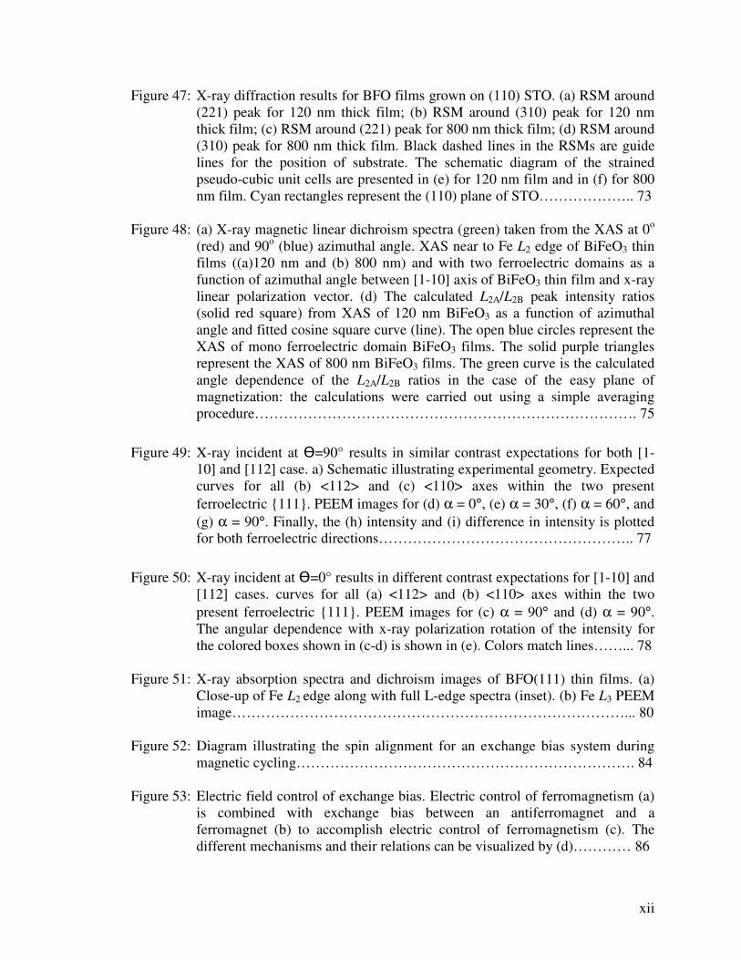
Figure 47: X-ray diffraction results for BFO films grown on (110) STO. (a) RSM around
(221) peak for 120 nm thick film; (b) RSM around (310) peak for 120 nm
thick film; (c) RSM around (221) peak for 800 nm thick film; (d) RSM around
(310) peak for 800 nm thick film. Black dashed lines in the RSMs are guide
lines for the position of substrate. The schematic diagram of the strained
pseudo-cubic unit cells are presented in (e) for 120 nm film and in (f) for 800
nm film. Cyan rectangles represent the (110) plane of STO……………….. 73
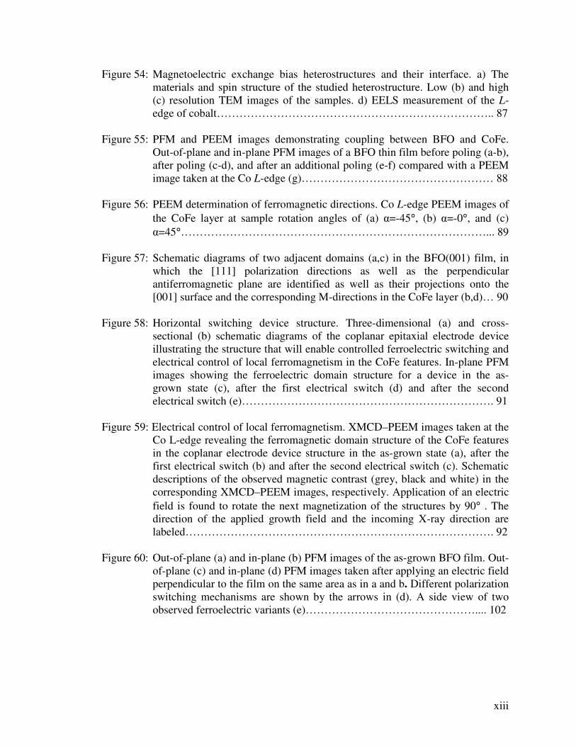
Figure 48: (a) X-ray magnetic linear dichroism spectra (green) taken from the XAS at 0o
(red) and 90o (blue) azimuthal angle. XAS near to Fe L2 edge of BiFeO3 thin
films ((a)120 nm and (b) 800 nm) and with two ferroelectric domains as a
function of azimuthal angle between [1-10] axis of BiFeO3 thin film and x-ray
linear polarization vector. (d) The calculated L2A/L2B peak intensity ratios
(solid red square) from XAS of 120 nm BiFeO3 as a function of azimuthal
angle and fitted cosine square curve (line). The open blue circles represent the
XAS of mono ferroelectric domain BiFeO3 films. The solid purple triangles
represent the XAS of 800 nm BiFeO3 films. The green curve is the calculated
angle dependence of the L2A/L2B ratios in the case of the easy plane of
magnetization: the calculations were carried out using a simple averaging
procedure……………………………………………………………………. 75
Figure 49: X-ray incident at �=90° results in similar contrast expectations for both [1-
10] and [112] case. a) Schematic illustrating experimental geometry. Expected
curves for all (b) <112> and (c) <110> axes within the two present
ferroelectric {111}. PEEM images for (d) α = 0°, (e) α = 30°, (f) α = 60°, and
(g) α = 90°. Finally, the (h) intensity and (i) difference in intensity is plotted
for both ferroelectric directions…………………………………………….. 77
Figure 50: X-ray incident at �=0° results in different contrast expectations for [1-10] and
[112] cases. curves for all (a) <112> and (b) <110> axes within the two
present ferroelectric {111}. PEEM images for (c) α = 90° and (d) α = 90°.
The angular dependence with x-ray polarization rotation of the intensity for
the colored boxes shown in (c-d) is shown in (e). Colors match lines……... 78
Figure 51: X-ray absorption spectra and dichroism images of BFO(111) thin films. (a)
Close-up of Fe L2 edge along with full L-edge spectra (inset). (b) Fe L3 PEEM
image………………………………………………………………………... 80
Figure 52: Diagram illustrating the spin alignment for an exchange bias system during
magnetic cycling……………………………………………………………. 84
Figure 53: Electric field control of exchange bias. Electric control of ferromagnetism (a)
is combined with exchange bias between an antiferromagnet and a
ferromagnet (b) to accomplish electric control of ferromagnetism (c). The
different mechanisms and their relations can be visualized by (d)………… 86
xiii
Figure 54: Magnetoelectric exchange bias heterostructures and their interface. a) The
materials and spin structure of the studied heterostructure. Low (b) and high
(c) resolution TEM images of the samples. d) EELS measurement of the L-
edge of cobalt……………………………………………………………….. 87
Figure 55: PFM and PEEM images demonstrating coupling between BFO and CoFe.
Out-of-plane and in-plane PFM images of a BFO thin film before poling (a-b),
after poling (c-d), and after an additional poling (e-f) compared with a PEEM
image taken at the Co L-edge (g)…………………………………………… 88
Figure 56: PEEM determination of ferromagnetic directions. Co L-edge PEEM images of
the CoFe layer at sample rotation angles of (a) α=-45°, (b) α=-0°, and (c)
α=45°………………………………………………………………………... 89
Figure 57: Schematic diagrams of two adjacent domains (a,c) in the BFO(001) film, in
which the [111] polarization directions as well as the perpendicular
antiferromagnetic plane are identified as well as their projections onto the
[001] surface and the corresponding M-directions in the CoFe layer (b,d)… 90
Figure 58: Horizontal switching device structure. Three-dimensional (a) and cross-
sectional (b) schematic diagrams of the coplanar epitaxial electrode device
illustrating the structure that will enable controlled ferroelectric switching and
electrical control of local ferromagnetism in the CoFe features. In-plane PFM
images showing the ferroelectric domain structure for a device in the as-
grown state (c), after the first electrical switch (d) and after the second
electrical switch (e)…………………………………………………………. 91
Figure 59: Electrical control of local ferromagnetism. XMCD–PEEM images taken at the
Co L-edge revealing the ferromagnetic domain structure of the CoFe features
in the coplanar electrode device structure in the as-grown state (a), after the
first electrical switch (b) and after the second electrical switch (c). Schematic
descriptions of the observed magnetic contrast (grey, black and white) in the
corresponding XMCD–PEEM images, respectively. Application of an electric
field is found to rotate the next magnetization of the structures by 90° . The
direction of the applied growth field and the incoming X-ray direction are
labeled………………………………………………………………………. 92
Figure 60: Out-of-plane (a) and in-plane (b) PFM images of the as-grown BFO film. Out-
of-plane (c) and in-plane (d) PFM images taken after applying an electric field
perpendicular to the film on the same area as in a and b. Different polarization
switching mechanisms are shown by the arrows in (d). A side view of two
observed ferroelectric variants (e)……………………………………….... 102
xiv
LIST OF SYMBOLS & ABBREVIATIONS
α – First order magnetoelectric coupling term
β – Higher order magnetoelectric coupling coefficient
γ – Higher order magnetoelectric coupling coefficient or interfacial energy
ε – Electric susceptibility
µ – Magnetic susceptibility
µ0 – Vacuum permeability
µB – Bohr magnetron, equal to 9.274096 x 10⁻²⁴ J/T
χe – Electric susceptibility
χm – Magnetic susceptibility
(x y z) – Miller indices for specific crystallographic plane
[x y z] – Miller indices for specific crystallographic direction
{x y z} – Miller indices for a family of equivalent crystallographic planes
<x y z> – Miller indices for a family of equivalent crystallographic directions
AEY – Auger electron yield
AFM – Antiferromagnet, Antiferromagnetic
ALS – Advanced Light Source
BFO – BiFeO3
CMR – Colossal magnetoresistance
CoFe – Co0.9Fe0.1
E – Electric field
e- – Electron
EB – Exchange bias

xv
EELS – Electron energy loss spectroscopy
EXAFS – Extended x-ray absorption fine structure
F – Free energy of a system
Fe – Iron
FE – Ferroelectric
FM – Ferromagnet
H – Magnetic field
HC – Coercive field
HEB – Exchange bias field
HRTEM – High resolution transmission electron microscopy
IP – In-plane
L – Sampling depth
LSDA – Local spin density approximation
LSDA+U – Local spin density approximation plus a Hubbard U parameter
M – Magnetization
ME – Magnetoelectric
NEXAFS – Near-edge x-ray absorption fine structure
OOP – Out-of-plane
P – Percentage of ferroelectric contribution to dichroism in a multiferroic
PEEM – Photoemission electron microscopy
PFM – Piezoresponse force microscopy
PLD – Pulsed laser deposition
Q – Percentage of magnetic contribution to dichroism in a multiferroic

xvi
RSM – Reciprocal space map
SRO – SrRuO3
STO – SrTiO3
TC – Ferroelectric or ferromagnetic Curie temperature
TEM – Transmission electron microscopy
TEY – Total electron yield
Ti – Titanium
TN – Néel temperature of an antiferromagnet
XANES – X-ray absorption near-edge spectroscopy
XAS – X-ray absorption spectroscopy
XLD – X-ray linear dichroism
XMCD – X-ray magnetic circular dichroism
XMLD – X-ray magnetic linear dichroism
XRD – X-ray diffraction

xvii
ACKNOWLEDGEMENTS
I would like to extend my deepest thanks to my qualifying exam committee Professors
Francis Hellman (Chair), Joel Moore and Yuri Suzuki and to Professors Joel Moore and
Yuri Suzuki for serving on my dissertation committee.
I would like to thank all of the people in the Ramesh group. My work would not be
possible without the assistance of many of my coworkers. Specifically, I thank Eddie
Chu, Tommy Conry, Chan-Ho Yang for growing samples for me. I thank Lane Martin for
not only growth of my samples but also of my scientific thought. I thank Helen He, Kate
Jenkins, and Sanni Kehr for working late nights with me. I also own much credit to
everyone who provided essential PFM support—Helen He, Nina Balke, Padraic Shafer,
Jan Seidel, Pei-Ling Yang, and Florin Zavaliche (now at Seagate). Let me also thank
post-docs Tong Zhao (now at Seagate) and Martin Gajek for passing on your expertise.
My research would have been much less fruitful and quite dull without the interaction
with many collaborators. Since no man is an island nor can know everything, only
through collaboration can we expect to answer the important questions of tomorrow.
Throughout this work, data collected with the help of such collaborations will be
presented. I would therefore like to specifically acknowledge the efforts of the following
individuals and groups for help with measurements and understanding. Andreas Scholl,
Jeffery B. Kortright, Elke Arenholz, and Andrew Doran from the Advanced Light Source
at Lawrence Berkeley National Laboratory for help with experiments and interpretation

xviii
concerning work done on BiFeO3, PbZrTiO3, LaSrMnO3, and many other materials.
Arantxa Fraile-Rodriguez, Frithjof Nolting, Loic Joly, and Cinthia Piamonteze at the
Swiss Light Source, Paul Scherrer Institut for help with photoemission studies on
Co/BiFeO3 and BiFeO3 crystals and thin films. Amit Kumar and Professor Venkat
Gopalan at Pennsylvania State University for fruitful discussions and interactions
concerning BiFeO3 as well as continued support and advice involving second harmonic
generation. Nicola A. Spaldin at the University of California, Santa Barbara for priceless
discussions about BiFeO3, tireless modeling assistance, and professional development
advice. Finally, and most importantly, Professor R. Ramesh – for your insistent guidance
whether or not I asked for it or wanted it. You have made me scientifically and personally
stronger than I ever thought possible.
Many thanks to the Department of Defense NDSEG Program for supporting the first
three years of my studies and for support from the SRC NRI Hans J. Coufal Fellowship
for support in my last two years. This work has been supported by the Director, Office of
Basic Energy Sciences, Materials Science Division of the U.S. Department of Energy
under Contract No. DE-AC02-05CH11231 and previous contracts, ONR-MURI under
Grant No. E21-6RU-G4 and previous contracts, and the Western Institute of
Nanoelectronics program.

1
Chapter 1: Complex Oxides and Their Complex Behavior
This chapter discusses some of the interesting properties and applications of complex
oxides. Material order parameters that can be controlled, such as magnetism and
ferroelectricity, are presented. Bismuth ferrite (BFO) is introduced as a system that has
both order parameters and the potential for coupling between these properties. The
central focus of this work--how to probe and control magnetism in model BFO films--is
raised in terms of its greater impact on everyday life and the world of materials science.
Finally, this chapter ends with a brief summary of the organization of this dissertation.

2
1.1 Complex Oxides
It is not common knowledge that complex oxides are an integral part of our daily lives.
Complex oxides are used to reduce the toxic emission in our automobiles, allow us to
check on the health of unborn babies by ultrasound, improve the performance of our
computers and video game consoles, and much more. In addition to being among the
most abundant minerals on earth, complex oxides give some of the most varied and
interesting properties,1 demonstrated by the table in Figure 1. These include their use as
dielectric and superconducting materials. Some complex oxides exhibit colossal
magnetoresistance (CMR), where enormous variations in resistance are produced by
small magnetic field changes, which would be useful for new technologies such as
read/write heads for high-capacity magnetic storage and spintronics.2 Magnetic and
ferroelectric properties are commonly exploited in power generation and computing.
A Site
B Site
Oxygen
Perovskite Structure – ABX3
eg
t2g
eg
t2g
eg
t2g
Figure 1 - Perovskite structure and variety of properties

3
Only recently has the research in the field of complex oxides flourished because these
materials were long thought to be too complex to fully understand. This complexity
comes from the strong coupling of charge, spin, and lattice dynamics, often resulting in
very full phase diagrams.2-3
Though the coupling may lead to complex behaviors, the
actual structure may be much simpler to describe. One common structure of complex
oxides is the perovskite form in Figure 1, where the A and B sites are typically different
cations and X is an anion (usually oxygen) that bonds to both. In several complex oxide
perovskites, this oxygen arrangement gives rise to a crystal field potential, hinders the
free rotation of the electrons and the orbital angular momentum by introducing the crystal
field splitting of the d orbitals.3 For example, the crystal field splitting illustrated in
Figure 1 shows the case for LaMnO3 where Mn3+
has a d4 configuration, meaning that
there are 4 electrons (represented by arrows) in the d orbitals. Due to Hund’s rule, all of
these spins point in the same direction, resulting in a total spin of 2. This is only the very
beginning of the story leading to the complexity in these systems. For a further discussion
of the detailed physics involved in this broad class of materials, see Tokura et. al.3
1.2 Controlling Order Parameters
1.2.1 Ferroelectricity
A particularly interesting subclass of complex oxides is materials with controllable order
parameters; for example, piezoelectric materials exhibit a response when in the presence
of an electric field, as demonstrated by a linear (dielectric) response in Figure 2a.
Ferroelectrics are a form of piezoelectric that remains polarized after the external electric

4
Figure 3 - Rhombohedral structure of
BFO at room temperature
field is removed.4-5
As is evident in the
hysteresis loop in Figure 2b, these
materials have a spontaneous
polarization at zero field, which can be
changed by application of an opposing
electric field.5-6
Thus, some companies have recently taken advantage of this hysteresis
behavior to build low energy memory devices.7 This hysteresis loop and resulting
behavior will disappear when the material goes above its ferroelectric critical temperature
Tc. Ferroelectrics are also commonly used to make tunable capacitors with high
capacitance, which make excellent sensors for use in ultrasound systems, high quality
infrared cameras, fire and vibration sensors, and even fuel injector.8
One ferroelectric that has recently received a
great deal of attention is bismuth ferrite (BiFeO3
or BFO). BFO is a rhombohedrally-distorted
perovskite ferroelectric with large intrinsic
polarization9 and eight possible polarization
directions occurring along the pseudocubic
111> body diagonals, one of which is shown in
Figure 3. Growth techniques (discussed in Appendix A) have been established to easily
select as many polarization directions as are desired for the application or experiment—
all eight, four, two, or even a single ferroelectric domain. Growth techniques also allow a
wide range of variance in other material parameters, such as strain, thickness, and
a) b)
Figure 2 - Electric field dependence for
a) dielectric and b) ferroelectric materials

5
1 µµµµm
[100]
Figure 4 - In-plane PFM image of BFO
thin film
orientation. The ferroelectric ordering temperature of BFO is also quite high (~1100K),
meaning that this material can perform well within a large range of temperatures.
The ferroelectric properties of BFO are most commonly studied by piezoelectric force
microscopy (PFM). PFM is a well-established technique that can image the in-plane and
out-of-plane projections of ferroelectric directions and can also switch the out-of-plane
(OOP) polarization direction.10-11
Thus, the polarization direction(s) of each of the
domains can be easily distinguished and compared to magnetic measurements. For more
details about PFM, please see Appendix B. Figure 4 is a typical in-plane image of BFO
thin films taken by PFM. For BFO thicknesses ~ 100 nm, the width of the ferroelectric
domains is ~ 150 nm. The white, brown, and
black contrasts correspond to the in-plane
projection of the ferroelectric domains. The
domain stripes align along [100] and the
projection of the ferroelectric directions are 45
degrees from the walls—pointing up, down,
left and right in Figure 4.12
1.2.2 Magnetism
Another order parameter that can be controlled is magnetism. The most commonly used
and understood magnetic order is ferromagnetism. It parallels ferroelectricity; whereas a
ferroelectric has a spontaneous polarization that can be changed by an applied electric

6
FE Ordering
AFM Ordering
a) b)
Figure 5 - Magnetic order in BFO with respect to
the [111] ferroelectric direction
field, a ferromagnet has a spontaneous magnetization that can be controlled by an applied
magnetic field. Ferromagnets are used for the memory in our computers, in power
generation and any time one needs a permanent magnet, such as on a refrigerator. There
are a large variety of methods for studying ferromagnets, such as superconducting
quantum interface devices, neutron studies, and x-ray magnetic circular dichroism.13
A form of magnetism that is more difficult to study is antiferromagnetism. An
antiferromagnet has no net magnetic moment. For example, BFO—in addition to its
ferroelectric properties—is also a G-type antiferromagnet, meaning that the individual
moments on each Fe-ion are aligned parallel within the pseudocubic {111} and
antiparallel between adjacent {111}. In BFO, there is a weak canting of ~1 degree
between the two sublattices (turned off in Figure 5a but on in Figure 5b), resulting in a
small magnetization of ~0.05 µB per unit cell.14
This small canting is allowed by the
Dzyaloshinskii-Moriya interaction,14
which results from the combined action of exchange
interaction and spin-orbit coupling.
Though antiferromagnets are less
thoroughly understood, they still find
valuable application in computing in the
pinning of ferromagnetic directions
called exchange bias. This concept will
be discussed in Chapter 6.

7
Since most magnetic characterization methods rely on measuring the net magnetic
moment, there are very few techniques to study antiferromagnetism. Most of the
techniques that do study antiferromagnetism are limited to averaging the magnetic
information over the entire sample. Since neutrons are magnetic, and are able to easily
penetrate through samples, reflected neutrons can be used to provide information about
the magnetic properties of individual layers or depth profiling. Second harmonic
generation probes the magnetic symmetry of antiferromagnetic materials, but averaged
over a large spot size. One of the few techniques that allows for the measurement of local
magnetic information is x-ray absorption studies; this method will be covered in greater
detail in Chapter 2.
1.2.3 Multiferroics and Magnetoelectrics
A particularly interesting case occurs when both ferroelectricity and magnetism are
present in the same material, creating one of a class of materials known as multiferroics.
A multiferroic is defined as a material that has at least two of the three following
properties—ferroelectricity, ferromagnetism, and ferroelasticity.15-16
Similar to the other
two order parameters, a ferroelastic has a spontaneous deformation that can be changed
by an applied stress. Multiferroics often come from the group of the perovskite transition
metal oxides, including rare-earth manganites and ferrites (e.g. TbMnO3 and HoMn2O5).
For example, BFO is a multiferroic that has all three ferroic properties at room
temperature. Therefore, BFO has been used as a model to study the interesting physics
and possible application that results from this trifecta of properties. In fact, BFO is the
only known material that is both magnetic and ferroelectric at room temperature, making
8
Figure 6 – Correlation of ferroelectric and
magnetic ordering (adapted from Ref. 19)
it an ideal candidate for devices. After some thought, this scarcity of other room
temperature multiferroics is not terribly surprising. Magnetic behavior requires partially
filled d electrons, whereas ferroelectrics typically have empty or filled d orbitals.17
Ferromagnets are often metallic, but ferroelectrics are insulators by definition. This point
illustrates why antiferromagnetic ferroelectrics are more common.
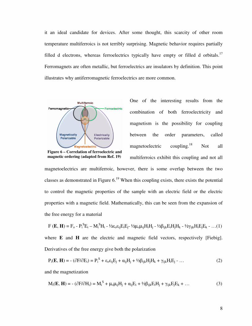
One of the interesting results from the
combination of both ferroelectricity and
magnetism is the possibility for coupling
between the order parameters, called
magnetoelectric coupling.18
Not all
multiferroics exhibit this coupling and not all
magnetoelectrics are multiferroic, however, there is some overlap between the two
classes as demonstrated in Figure 6.19
When this coupling exists, there exists the potential
to control the magnetic properties of the sample with an electric field or the electric
properties with a magnetic field. Mathematically, this can be seen from the expansion of
the free energy for a material
F (E, H) = Fo - PiSEi – Mi
SHi - ½εoεijEiEj- ½µoµijHiHj - ½βijkEiHjHk - ½γijkHiEjEk - …(1)
where E and H are the electric and magnetic field vectors, respectively [Fiebig].
Derivatives of the free energy give both the polarization
Pi(E, H) = - (∂F/∂Ei) = PiS + εoεijEj + αijHj + ½βijkHjHk + γijkHiEj - … (2)
and the magnetization
Mi(E, H) = - (∂F/∂Hi) = MiS + µoµijHj + αijEi + ½βijkEiHj + γijkEjEk + … (3)

9
where ε and µ are the electric and magnetic susceptibilities and α is the induction of
magnetization by an electric field or polarization by a magnetic field. Though higher
orders of ME effects are possible, the linear ME effect (α) is generally much larger. For
example, bulk BFO is known to have no linear ME effect, due to a canceling of the
magnetic order due to a spin spiral. In thin films, however, it is possible to discourage
this canceling by proper control of the growth parameters, thus allowing a linear ME
effect. This could potentially provide a dramatic improvement to the ME effect in BFO
thin films.
Magnetoelectric coupling has many potential applications in computing, sensors, and
energy scavenging.20
For example, the 0’s and 1’s that make up the memory of computers
are just magnetic domains. The magnetization direction within each domain is written by
application of a magnetic field. However, there are many problems with using magnetic
fields if we are going to continue to make computers smaller, faster and more energy
efficient. Magnetic fields require a great deal of power to generate, and these fields can
also be difficult to localize, limiting the minimum size of the bit and the memory density.
Additionally, the speed that these magnetic fields are applied can only be reduced so far,
since the ultrafast motion of spins excited by field pulses shorter than thermal relaxation
times (~100 ps) are poorly understood. If one instead uses a material where the
magnetism can be controlled electrically, many of these issues can be resolved.
10
1.3 Understanding and Controlling Magnetism
The goal of this work is to understand and control magnetism in BFO thin films. Though
the magnetic order of bulk BFO has been well characterized, little work on thin films was
attempted. This thesis describes how x-ray absorption measurements where used to
determine the specific magnetic order on a range of thin films and study the effect of this
order on a ferromagnetic layer on top of BFO. This work will further the understanding
of magnetic ordering in antiferromagnets and their influence in exchange bias. The thesis
is organized as described below. Chapter 2 details the physics behind the x-ray absorption
technique utilized in this study. Chapter 3 describes how we and other groups were able
to prove that not only are the magnetic and ferroelectric domains in both thin films and
crystals of BFO coupled, but that they continue to be after perturbation with an electric
field. Chapter 4 discusses how we can change the magnetic properties of BFO through
film thickness and strain. The presented measurement techniques are applicable to
understanding order parameters in a wide range of materials that are often difficult to
measure. Chapter 5 investigates the role of different crystallographic orientations and
how they affect both the understanding and control of the magnetic order parameter. In
Chapter 6, the use of this collection of control parameters to electrically control
ferromagnetism through coupling a ferromagnetic to magnetoelectric BFO thin films is
explored. Chapter 7 serves as a summary chapter recapping the findings presented in each
chapter and proposing future work in this area. Appendix A covers some of the important
details concerning the growth of BFO films. Appendix B focuses on how PFM is used to
understand the ferroelectric nature of BFO and other films.

11
Chapter 2: The Technique Behind Probing Magnetism—X-ray Absorption
This chapter explores the history, importance and physics behind x-ray absorption and
dichroism. X-ray absorption spectroscopy, total electron yield, photoemission electron
microscopy techniques are discussed. Advantages and disadvantages of several
photoemission electron microscopes utilized in this work are compared. The origin of
circular and linear dichroism is explored through example in NiO systems. Finally, the
power of PEEM is demonstrated by the application of both circular and linear dichroism
to study coupling between different materials.

12
2.1 Synchrotron Radiation History
Arguably the strongest resource for material characterization was not even originally
intended for that purpose. A synchrotron is a type of particle accelerator which utilizes
magnetic and electric fields to accelerate particles around nearly circular paths to speeds
extremely close to the speed of light. Particle physicists have used particle accelerators to
collide particles and learn about the dynamics and structure of matter, space and time.
The problem (and opportunity) with accelerating particles to such high speeds is that the
particles give off large amounts of radiation in the form of photons. Ivanenko and
Pomeranchuk published their 1944 calculations showing that these energy losses would
limit the energy obtainable by early particle accelerators, called betatrons. This predicted
limitation prompted scientists such as Blewett to search for these energy losses, but little
success over the years lead many to believe synchrotron radiation was not the source of
the loss. A clever design by General Electric on another kind of particle accelerator,
called a cyclotron, allowed the first observation of synchrotron radiation. The doughnut-
shaped electron tube was made transparent in order to allow technicians to test an
intriguing property for this type of accelerators called bunching. Instead, a bright arc of
light was observed, which General Electric researchers quickly realized was coming from
the electron beam. Langmuir is credited as first recognizing the arc as synchrotron
radiation. After its discovery, several facilities introduced small beamlines to take
advantage of the energy losses that were once considered a nuisance. Though synchrotron
radiation was initially only a parasitic branch of particle accelerators claiming only a
small percentage of the available beamtime, today dedicated facilities exist to foster the

13
growing demand for synchrotron measurement. It is intriguing to realize that even though
synchrotron radiation is as old as the stars—for example causing the light we see from
the Crab Nebula—only in the last several decades have we recognized and manipulated
its opportunities.21
2.2 Polarized X-rays
The radiation that comes from the synchrotron has several advantages: it has much higher
flux than can be achieved by standard laboratory techniques (also many orders of
magnitude greater than the sun), its energy range is tunable within a ~1000 eV range, and
the photons are polarized. There are two common methods to collect these photons: using
a bending magnet or an undulator. Since both were employed for the following
measurements, the differences between the two techniques should be considered.
Bending or dipole magnets are commonly used in particle accelerators to inject or eject
particles into or out of the accelerator. Bending magnets are cheaper to construct than
undulators, though their flux is generally four orders of magnitude less than would be
achieved from an undulator. Bending magnets can produce light that is linearly polarized
and right or left circularly polarized. An elliptically polarizing undulator (EPU) produces
these three polarizations as well; however, it can also rotate the light polarization by
ninety degrees in fine steps if desired. Though this rotation of the light polarization is
vital for some of the measurements presented in Chapter 4, many of the other
measurements can be obtained without an EPU.

14
2.3 Experimental Techniques
2.3.1 X-ray Absorption Spectroscopy
One of the techniques that take advantage of the polarized x-rays provided by bending
magnets and undulators is x-ray absorption spectroscopy (XAS), which is used for
molecular and condensed matter physics, biology, chemistry, earth science and more. X-
ray absorption spectra are taken by varying the energy of incident photons in a range (0.1
– 100 keV) where core electrons are excited. Depending on the quantum number (n=1, 2,
and 3) of the excited electron, the spectra will have different names, respectively the K-,
L-, and M-edges. This work will focus on the excitation of 2p electrons or the L-edge.
There are two regions of XAS spectra that are commonly utilized. This work makes use
of the dominant features called XANES (X-ray Absorption Near-Edge Spectroscopy) or
NEXAFS (Near-edge X-ray Absorption Fine Structure) which, when used in
combination, provide information on the local electronic states and their modification by
local chemistry. The EXAFS (Extended X-ray Absorption Fine Structure) region is above
the XANES region and occurs whenever the absorbing atom is closely surrounded by
other atoms. For example, noble gases and monatomic vapors will exhibit no EXAFS.
The EXAFS can provide radial locations, coordination numbers, atomic type
differentiation, and disorder estimates for near neighbors surrounding the central
absorbing atom.
15
2.3.2 Total Electron Yield
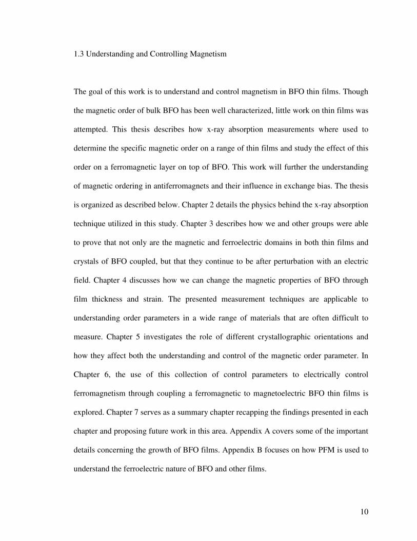
NEXAFS spectra and images are gathered by a technique called total electron yield
(TEY), which is visualized in Figure 7. Instead of directly measuring the absorbed x-ray
intensity, the photoelectrons that are created by the absorbed x-rays are observed.
Absorption takes place when the core electrons are excited to empty states above the
Fermi level (Figure 7a). These excited photoelectrons recombine with the core states by
emitting a primary Auger electron (Figure 7b), with the intensity of these Auger electrons
being a direct measure of the x-ray absorption. Auger electrons are used in a similar,
extremely surface sensitive (too much so for some purposes) technique called Auger
electron yield (AEY). Following the primary Auger electron emission, the photoelectron
and Auger electron can be excited above the vacuum level—and thus emitted off of the
sample—or lose energy through inelastic scattering due to their small mean free path
(Figure 2c). In the latter case, a large number of secondary electrons are created for each
photoelectron (Figure 2d); these secondary electrons dominate the TEY intensity as seen
in Figure 2e. Electrons formed deep in the sample lose much of their energy through
multiple scattering events and do not contribute significantly to the TEY. Thus, the
a) b) c) d) e)x-rayse-
sampling
depth Le-Photo e-
Auger
e-out
secondary
electrons
Auger- and
Photoelectrons
Electron Kinetic Energy
Ele
ctro
n Y
ield
x100
Figure 7 - Total electron yield description. a)-c) illustrate the excitation and decay of electrons in
TEY. d) One x-ray creates several secondary electrons within the sampling depth L. e) These
secondary electrons dominate the TEY intensity. (adapted from Ref. 22)
16
sampling depth for TEY is approximately ten nanometers, or five times greater than that
of AEY measurements.22
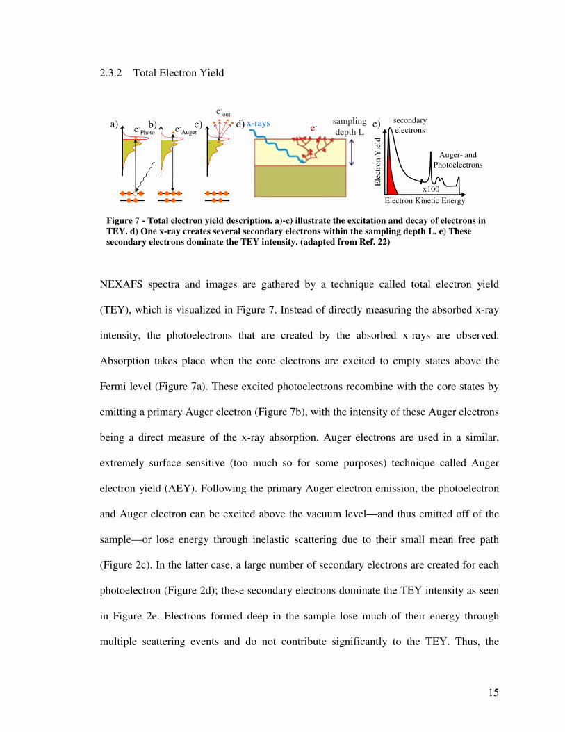
2.3.3 Photoemission Electron Microscopy
Photoemission electron microscopy (PEEM) is a technique for collecting the TEY that
spatially displays the intensity map of the collected photoelectrons. Though cathode-lens
microscopy was introduced in the 1930s by Bruche et. al.,23
PEEM has become a
practical tool only recently due to current technological developments.24
Much was
learned from Bauer et. al.,25
whose work in the very similar technique of low energy
electron microscopy (LEED) spurred further growth with PEEM. The availability and
increased use of high performance synchrotron radiation in the late 1980s, the
development of ultrahigh vacuums in emission microscopy, and the success of electron
yield based absorption spectroscopy were all helpful to the PEEM proposal of Tonner
and Harp26
and Engel et al.27
a few years later.
In PEEM measurements, the radiation of monochromatic x-rays with energies larger than
the work function of the material of interest cause the emission of photoelectrons off of
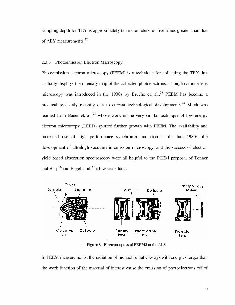
Figure 8 - Electron-optics of PEEM2 at the ALS
17
the sample’s surface. These electrons are accelerated into an electron-optical imaging
device by an electric field. The optics (including objective, transfer, intermediate and
projector lens) are used to image electrons onto a phosphor detector that converts them
into visible light, which is finally read by a CCD camera. Figures 8 and 9 show the
optical layout of beamline 7.3.1 at the Advanced Light Source (ALS) and the PEEM2
setup, respectively.28
The PEEM work presented was completed at three different beamlines. PEEM2 was the
only available PEEM for the first half of the work. This PEEM, which lies on the end of a
bending magnet, has low flux, low resolution (~100 nm), and only horizontal linear light
polarization. Later, access to the PEEM at the Swiss Light Source (SLS) allowed both
sample and light polarization rotation, although slightly lower resolution (~150nm).
Finally, an upgraded PEEM was brought online at the ALS (PEEM3). This PEEM has
light polarization rotation and resolution down to ~20 nm, but access to it has been
limited due to both great interest by the scientific community and several technical issues.
Figure 9 - Beamline setup at 7.3.1 at ALS

18
When planning experiments, careful attention was made to select the correct PEEM for
the purpose, since they all have their own advantages and disadvantages.
2.4 X-ray Absorption Line Shape
2.4.1 The Golden Rule and Selection Rules
The importance of PEEM is intimately linked with the importance of XAS. Though XAS
and PEEM do not offer the wonderful spatial resolution of some other techniques—such
as transmission electron microscopy—they do present the ability to nondestructively
measure magnetic moments with elemental and chemical specificity. The origin of this
sensitivity is the conservation of energy and angular momentum. The x-ray absorption
cross section for a material is governed by Fermi’s Golden rule:
| < f | ez | i > |2 δ(Ef − Ei − ħω) (4)
where ez is the dipole operator. For the transition from the initial state | i > to the final
state | f> to occur, the energy of the incoming x-ray has to be equal to the energy
difference between two possible electronic states. This is energy conservation. We can
also determine the intensity of the transition by calculating |< f | H | i > |2, where H is the
system’s Hamiltonian. This can be calculatedly exactly, if the initial and final wave
functions are known. But even in general, we can gain information as to the possible
transitions from the symmetry of the dipole operator and its exchange properties with the
spin operator S and the angular momentum L derived by spin-orbit coupling. For an
unpolarized x-ray, absorption only occurs at ∆S = 0, ∆L = ±1. Only optical transitions
that do not change the spin of the system but do change the angular momentum by one

19
are observed. This limits the number of possible transitions. There is another set of
transition rules for polarized x-rays which are more important for the study of magnetic
materials: the electronic states in these systems are not evenly populated and have
different orientations, causing a dichroism effect. Dichroism refers to changes in the
absorption of passing polarized light of different directions. The origin of the dichroism
effect can be anisotropies in the charge or the spin in the material. The latter case is
magnetic dichroism, which has been used to study magnetic materials for over a century
in the magnetic optic Kerr effect. However, using x-rays to investigate this dichroism is a
more recent approach.
2.4.2 Elemental Specificity
Additional advantages of XAS and PEEM include submonolayer surface sensitivity, the
capability to investigate many nanometers of the surface of a material when combined
with x-ray magnetic dichroism, and the ability to identify elements and their chemical
state.24
The usefulness of PEEM in elemental identification is due to the fact that the
electron binding energy is highly dependent on the charge of the nucleus; even though the
absorption line shapes are
similar for several elements,
they can be differentiated by
the energy at which they
occur. This can be seen in
Figure 10, which shows the
x-ray absorption spectra at Figure 10 - Plot of total electron yield for wedge Cu/Fe/Ni sample
22

20
various points along a wedge of copper, iron, and nickel. As the iron layer thickness is
increased, the iron signal increases since there is more iron to probe, while the nickel
signal decreases because of the limited electron escape depth of the TEY technique. The
copper layer, which is above the iron
layer, produces a constant signal,
reflecting its constant thickness. X-ray
absorption spectroscopy provides
information on the chemical
environment of the atoms and their
magnetic state, since core electrons are
excited in the absorption process into empty states above the Fermi energy. The
electronic and magnetic properties of the empty valence levels are therefore probed.
The L-edge x-ray absorption edge spectra of Fe, Co, and Ni in the metallic as well as in
an arbitrary oxidation state are shown in Figure 11. Magnetic properties of these
materials are largely determined by the 3d valence electrons. The two principle peak
clusters are the L3 (left) and L2 (right) absorption edges. L-edge absorption studies (2p to
3d transitions) best determine the d-shell properties, since x-ray absorption spectra are
governed by dipole selection rules. The two spectra peaks originate from the spin orbit
interaction of the 2p core shell, and their total intensity is proportional to the number of
empty 3d valence states. The width of the empty d-bands can be determined by the
distance between the metal spectra peaks (roughly 15 eV). Oxides exhibit a considerable
amount of fine structure in their spectra, called multiplet structure. The reason for this is
Figure 11 - L-edge x-ray absorption edge spectra
22

21
that the empty oxide states are more localized than metal states and their energies are
determined by crystal field and multiplet effects. Origins of multiplet effects are the spin
and orbital momentum coupling of different 3d valence holes or electrons in the
electronic ground state and the coupled states formed after x-ray absorption between the
3d valence holes and the 2p core hole.28
2.4.3 X-ray Magnetic Circular Dichroism
Van der Laan predicted circular and linear x-ray magnetic dichroism (XMCD and
XMLD) in 3d transition metals in 1991.29
The TEY-XAS for two circular polarizations in
red and blue for the L edge of iron is shown in Figure 12. The difference between the left
and right circular absorption lines gives the XMCD signal. The areas under the A2 and A3
curves are a measure of the magnetic polarization with respect to the direction of the
incident light. XMCD attracted more attention once the so-called sum-rules were
established; these rules relate the intensity of the dichroism to the orbital and spin
moments and the spin density.30
One can even determine the absolute magnetic moments
per atom if the number of holes is known.
Figure 12 - Typical Fe XAS and XMCD
22 Figure 13 - Origin of spin and orbital moment
22
sensitivity

22
The concepts behind the sum rules for XMCD spectroscopy are demonstrated in Figure
13.28
The first sum rule relates the number of empty d states (maximum of ten) to the
total intensity of the L3 and L2 resonances. The spin dependency of x-ray absorption can
be used to determine the difference between the number of spin up and spin down holes
(the absence of these electrons), and the spin imbalance of spin up and spin down
electrons of a magnetic material gives rise to a spin moment. Incident left or right
circularly polarized photons transfer angular momentum to excited photoelectrons, which
take this momentum as spin or angular momentum or a combination.28
If the
photoelectron came from a spin-orbit split level, such as p1/2 which is related to the L2
edge, the partial or full transfer from angular momentum to spin occurs due to spin-orbit
coupling. There is an opposite contribution for left circularly polarized photons with
respect to right circularly polarized photons, meaning photoelectrons of opposite spins
are created. Spin polarization will be opposite in the L2 and L3 edges since spin-orbit
coupling in p1/2 and p3/2 are opposite. Electric dipole transition selection rules do not
allow photoelectrons excited to d hole states from p shells to change spin, and thus the
transition intensity is proportional to the number of d holes of the desired spin. The
dichroism effect is maximized when the signal when the magnetization direction and
photon spin are parallel is compared to when they are antiparallel. Through sum rules, the
L2 and L3 intensities and differences can be linked to the number of d holes and the size
of the spin and orbital magnetic moments. Additional information on the spin and orbital
anisotropies of the material31
is determined by changing the angle of the applied magnetic
field relative to the sample.

23
2.4.4 X-ray Magnetic Linear Dichroism
Circular dichroism provides magnetic information for ferromagnetic materials, but gives
no signal or data for antiferromagnetic materials. As mentioned before, very few
techniques—particularly ones that provide information on the spin orientation—are
available for antiferromagnets. X-ray magnetic linear dichroism (XMLD), which is a
similar technique to XMCD, was developed by van der Laan in the 1980s and is best
understood by example. Hendrik Ohldag et al. of the Stanford Synchrotron Radiation
Laboratory investigated antiferromagnetic domains of an ultra thin layer of NiO on argon
(100) and gold (111).32-33
This was first done using the BESSY II storage ring in Berlin,
but the experiment was later confirmed and improved upon using the PEEM2 system, as
will be discussed in the next example. NiO is a G-type antiferromagnet, which means that
it aligns ferromagnetically along its 111 planes and antiferromagnetically between
adjacent planes. There are four different domains associated with the four different 111
planes, which split up further due to the threefold symmetry of the 111 planes. Twelve
domains are characterized by antiferromagnetic axis A, which points parallel to the
difference of the sublattice magnetizations.
Figure 14 - L2 linear Ni edge
32 Figure 15 – Contrast vs. azimuthal angle
32

24
Figure 14 shows the TEY of the nickel L2 edge XMLD spectra for a 30 monolayer thick
film. The XMLD effect is angle-dependent due to the preferential orientation of the
antiferromagnetic axis A, which can be seen from the signals at different azimuthal
orientations (Figures 14 and 15). In this case, peak A is larger than B when the electric
field of the incident x-rays (E) is perpendicular to A, and smaller when parallel, as in
many other films. As completed in Figure 16, AFM domains can be observed by dividing
a PEEM image acquired at peak B by the image taken at peak A.34
This division of
images cancels most background noise.
The strong magnetic contrast in Figure 16 comes
from magnetic domains with an in-plane
projection of the antiferromagnetic axis either
parallel (light) or perpendicular (dark) to the
horizontal electric field vector, circled in Figure
15. Domains are not seen when the sample is
rotated by forty-five degrees from parallel or
perpendicular because the in-plane projection is
equal for both orientations. Due to experimental
geometry, domains rotated by 180 degrees about
the surface normal can not be distinguished from
each other. Figure 15 also reveals that the maximum contrast occurs when the electric
field of the light is forty-five degrees from the [001] or [010] directions in the crystal
Figure 16 - XMLD image B/A
32

25
surface. Therefore, the magnetic moment directions shown in Figure 16 are roughly
forty-degrees to the strip patterns, which has widths around 10 µm (larger than expected
for epitaxial thin films).35-36
Larger domain sizes will be useful in applications; we will
explore one such example shortly.
Studies of the temperature
dependence reveal that the
image contrast is reduced at
higher temperatures and can
be reversed by cooling as
seen in Figure 17. In this
case, it is customary to
assume that no chemical or
diffusive processes are affecting the sample’s surface magnetic state at these
temperatures. Since the domain pattern is not changed, stresses from the bulk domains
are the likely cause of the size and topology of the domains. The antiferromagnetic
contrast has a parabolic temperature dependence, which disappears above the sample’s
Neel temperature of 530K. This agrees with low energy electron diffraction
measurements of magnetic superstructure reflections, which also show a signal
proportional to the square of the antiferromagnetic order parameter. This technique
allows simultaneous determination of multiple antiferromagnetic domains as well as
investigation into their origin.
Figure 17 - NiO AFM contrast temperature dependence from
Ni L2-edge fine structure with superimposed theory curves.

26
2.4.5 Combining XMCD and XMLD
Though these techniques (XMCD and XMLD) are utilized to individually study
ferromagnetic and antiferromagnetic domains, they can also be combined to study
coupling between different materials. For example, Chapter 6 will discuss our study of
the coupling between the electrically controllable antiferromagnetism of BFO and a
ferromagnetic layer. There has recently been a great deal of experimental37
and
theoretical38
interest in using standard antiferromagnetic thin films to pin the
magnetization direction of a ferromagnetic layer, due in part to their usefulness in spin
valve devices.39
This effect is known as exchange bias and will be discussed further in
Chapter 6. Even after extensive research, little is known about this effect since there are
very few techniques that provide information
on arrangement of magnetic moments near an
interface. PEEM is a unique way to measure
this kind of system since it is sensitive to the
magnetic vectors in both the ferromagnet and
the buried antiferromagnetic layers.40
Let us consider an example very similar to
the previous antiferromagnet example.
Ohldag et al. also studied the result of
growing ferromagnetic cobalt in situ by
electron beam evaporation on top of the antiferromagnet NiO.41
The fine structure in the
L-edges of Ni and Co in Figure 18, recorded by tuning to the appropriate energy (870 eV
Figure 18 - L edges of Ni and Co for sample
and metal and expected oxidation state41

27
and 780 eV respectively) allow one to distinguish between the metal and oxidation
states. Also included in the graphs for comparison are the structures expected from Ni
metal, Co metal, NiO, and CoO. This data shows evidence of interfacial diffusion effects
which are likely to change the magnetic structure at the interface. For example, notice
that the Ni edge signal looks more like the expected signal for Ni, rather than NiO. It is
known that the material below is NiO, meaning the amount of NiO has been reduced at
the interface with Co. This is likely due to uncompensated spins from an interface layer
that is either ferromagnetic or ferrimagnetic. Linear dichroism was used to study the
antiferromagnet NiO by dividing peaks A and B (as before), while circular dichroism was
used to study the ferromagnet Co by dividing the images at the L3 and L2 peaks. The
limited sampling depth and small
thickness of Co combine to allow
interface sensitivity. Using the photon
energy at peak A emphasizes the Ni-
metal component. By using circular
polarization and dividing the resulting
right and left circularly polarized images
as shown in Figure 19, one can hunt for
uncompensated spins. The signals in
Figure 19 are the XMCD of Co (top), Ni
(middle), and the XMLD of NiO
(bottom). The ellipses on the left are a
key for the domain orientations. It is
Figure 19 - XMCD of Co (top) and Ni (middle) and
XMLD of NiO (bottom) with 45° rotation41
28
important to note that the antiferromagnetic domain walls are parallel to the in-plane
[100] directions and the in-plane projection of the incident k vector is parallel to [110].
The two geometries given in Figure 19 are rotated 45 degrees from each other.
Otherwise, the signals are from the same sample position. The middle image of the top
orientation seems to be a superposition of the XMCD Co and XMLD Ni L edges. As the
circular polarization at PEEM2 is not perfectly circularly polarized, there is a small
component of linear polarization from the in-plane component of the circularly polarized
x-rays. For this reason, we see the antiferromagnet NiO stripes in the XMCD Ni L edge.
But if one rotates the sample by 45 degrees, the linear dichroisms goes away and thus so
do the stripes. The FM Ni signal (middle) of the rotated sample now shows exactly the
same domain patterns as Co does. Before deposition of Co the structure looked different,
and therefore it can be surmised that the addition of Co creates and aligns uncompensated
spins.
This is further supported by the
increasing number of interfacial
spins with increasing time in an
annealing temperature of 600K,
which is higher than the
material’s Neel temperature.
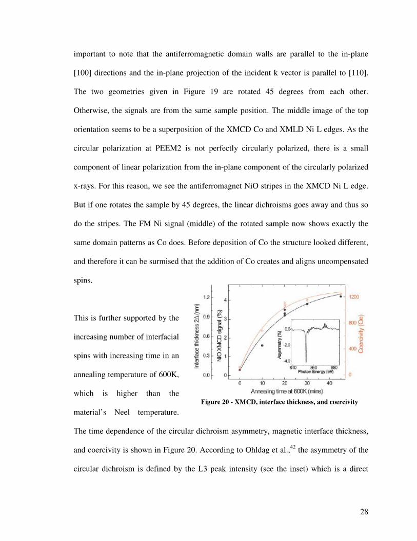
The time dependence of the circular dichroism asymmetry, magnetic interface thickness,
and coercivity is shown in Figure 20. According to Ohldag et al.,42
the asymmetry of the
circular dichroism is defined by the L3 peak intensity (see the inset) which is a direct
Figure 20 - XMCD, interface thickness, and coercivity
29
measure of the Ni spin moment. The interfacial moment and thickness increase with time
up to some saturation. This happens because the oxygen concentration at the interface,
where this takes place, starts out large but decreases as the oxygen diffuses into the Co.
The coercivity, measured by magneto-optical Kerr effect, does not go above 1350 Oe. It
also follows the same pattern as the interface thickness, as shown in Figure 20.
Previous studies of exchange bias have considered several possible origins of the
uncompensated spins, such as termination of the bulk structure,43
spin-flop canting of
AFM spins,44
and defect-oriented effects.45-46
Ohldag et al. instead show that in NiO/Co
the existence of an interface layer creates uncompensated spins, which govern the
coercivity increases and exchange bias. Annealing time increases the interface thickness
and coupling strength. This example is clearly a good demonstration of the power of
PEEM and x-ray absorption.
Current PEEM setups have the ability to resolve 20 - 1000 nm antiferromagnetic domains
in thin films, which is an important capability for further understanding of the science of
surface magnetism. The capability of PEEM to study both XMCD and XMLD makes it
ideal for the examination of individual magnetic materials as well as ferromagnetic-
antiferromagnetic interfaces to study exchange bias,40
the interaction between a
ferromagnetic and antiferromagnetic layer.34
There is still much to learn about the
surfaces and interfaces of magnetic materials. PEEM is an indispensable tool for this
research due to its ability to simultaneously give information regarding magnetic

30
moments and the Neel temperature along with highly resolved images of magnetic
domains.
31
Chapter 3: Electric Control of Antiferromagnetism
The possibility to electrically control magnetism is extremely interesting from both a
physics and application perspective. This chapter discusses the existence of such coupling
in BFO thin films. The chapter starts with a theoretical discussion on how such electrical
control could occur. The possible ferroelectric switching mechanisms are introduced and
illustrated through PFM measurements. PEEM is used as a tool to provide insight on the
magnetic properties of BFO. PEEM’s sensitivity to ferroelectricity as well as magnetism
is introduced and investigated through thorough temperature dependence. Electrical
control of magnetism is demonstrated by comparing as-grown and electrically switched
PFM and PEEM images of BFO thin films. Finally, this work was confirmed by electrical
control of magnetism in BFO crystals by Lebeugle et. al.

32
3.1 Theory of Electric Control of Magnetism in BFO
As discussed in sections 1.2.1-3, BFO is an excellent model system for the study of
parameter coupling. Though BFO was known to be the only room temperature magnetic
ferroelectric, there was no information on magnetoelectric coupling in these films—
whether it was possible to electrically control magnetism or vice versa. Spaldin’s LSDA
calculations14
were the first to strongly suggest that such multifunctional control could be
possible in BFO films. These calculations found that (a) the energy was minimized when
the antiferromagnetic axis lie in the plane perpendicular to the BFO polarization direction
and (b) weak ferromagnetism (which has been observed in BFO films) is only allowed by
symmetry when the magnetism lies in this perpendicular plane.
EEEEEEEE
PPPP1111++++PPPP1111++++
Bi
Fe
O
Bi
Fe
O
PPPP1111----
180°
PPPP1111----
180°
PPPP4444----
109°
PPPP4444----
109° PPPP3333----
71°
PPPP3333----
71°
a)
b) c) d)
[001][001]
Figure 21 - Schematic diagram of (001)-oriented BiFeO3 crystal structure and the ferroelectric
polarization (bold arrows) and antiferromagnetic plane (shaded planes). a) Polarization with
an up out-of-plane component before electrical poling. b) 180◦ polarization switching
mechanism with the out-of-plane component switched down by an external electrical field. The
antiferromagnetic plane does not change with the 180◦ ferroelectric polarization switching.
109◦ (c) and 71◦ (d) polarization switching mechanisms, with the out-of-plane component
switched down by an external electrical field. The antiferromagnetic plane changes from the
orange plane to the green and blue planes on 109◦ and 71◦ polarization switching respectively.

33
Perpendicular magnetism could potentially have a very interesting consequence for BFO
films. If one can force the polarization direction to change to one of the other 111 body
diagonals, the initial perpendicular plane is no long perpendicular and a new
perpendicular magnetic plane should form, thereby controlling the magnetism. Control of
the ferroelectric domains in BFO films is indeed possible by the application of a ~12 V
vertical electric field using PFM. As demonstrated in Figure 21, application of a vertical
electric field can result in three types of switching—180°, 109°, and 71°. In the case of
180° switching, the initial and resulting perpendicular magnetic plane are the same, so no
change in magnetism is required. However, the 71° and 109° switching should result in a
magnetic plane change.
3.2 Ferroelectric Switching of BFO
All three types of switching—180°, 109°,
and 71°—are possible using PFM. Figure
22 shows PFM images taken in the same
location before (a and b) and after (c and
d) electric field poling of a 10 by 10 µm
box. As described in Appendix B, the
colors in the out-of-plane (a and c) and in-
plane (b and d) images are used to
determine the ferroelectric direction, the
projections of which are shown by the
⊗⊗⊗⊗ ••
71°180°
109°
5×5 µm2 5×5 µm2
5×5 µm25×5 µm2
a) c)
b) d)
Figure 22 - Out-of-plane (a) and in-plane (b)
PFM images of the as-grown BFO film. Out-
of-plane (c) and in-plane (d) PFM images
taken after applying an electric field
perpendicular to the film on the same area as
in a and b. Different polarization switching
mechanisms are described in the table.
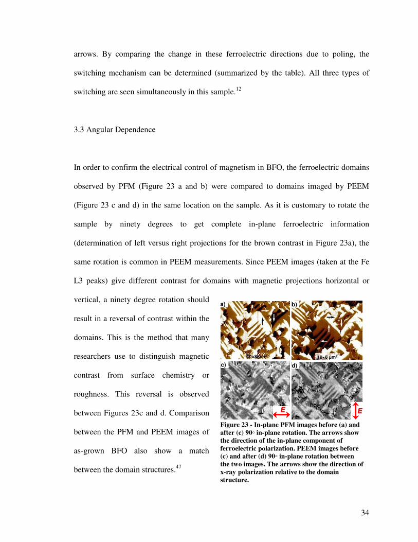
34
arrows. By comparing the change in these ferroelectric directions due to poling, the
switching mechanism can be determined (summarized by the table). All three types of
switching are seen simultaneously in this sample.12
3.3 Angular Dependence
In order to confirm the electrical control of magnetism in BFO, the ferroelectric domains
observed by PFM (Figure 23 a and b) were compared to domains imaged by PEEM
(Figure 23 c and d) in the same location on the sample. As it is customary to rotate the
sample by ninety degrees to get complete in-plane ferroelectric information
(determination of left versus right projections for the brown contrast in Figure 23a), the
same rotation is common in PEEM measurements. Since PEEM images (taken at the Fe
L3 peaks) give different contrast for domains with magnetic projections horizontal or
vertical, a ninety degree rotation should
result in a reversal of contrast within the
domains. This is the method that many
researchers use to distinguish magnetic
contrast from surface chemistry or
roughness. This reversal is observed
between Figures 23c and d. Comparison
between the PFM and PEEM images of
as-grown BFO also show a match
between the domain structures.47
EEE
c)
EEEE
d)
a) b)
10×8 µm2 10×8 µm2
Figure 23 - In-plane PFM images before (a) and
after (c) 90◦ in-plane rotation. The arrows show
the direction of the in-plane component of
ferroelectric polarization. PEEM images before
(c) and after (d) 90◦ in-plane rotation between
the two images. The arrows show the direction of
x-ray polarization relative to the domain structure.

35
3.4 Ferroelectric Contrast in PEEM
Examining the data presented to this point, it is tempting to conclude that the magnetic
domains match with the ferroelectric domains. This has not yet been proven, however;
unfortunately, it was found that a dichroic contrast can also be observed due to
ferroelectricity. In order to study the dichroic nature of ferroelectricity, consider a pure
ferroelectric material periodically poled lithium niobate (PPNL).
As seen in Figure 24, a very
similar approach to that employed
for BFO was used to study the
ferroelectric contribution to
dichroism in PPNL single crystals.
A PEEM image (a) is compared to
the AFM (b) and PFM (c) images
in PPNL with a periodicity of
patterned domains ~6.8 µm. The
bright spots in the image may be
dust particles or other foreign
materials.48
The bright regions in
the PEEM image are negative
domains (domains with negative surface polarization charges), while the darker regions
are positive domains.48
Though the PEEM resolution is not quite as detailed, it is clear
Figure 24 - (a) PEEM, (b) AFM and (c) PFM images of
PPLN. The fields of view are 40 µm. Insets in (b) and
(c) are 10x10 mm2 and obtained from the same surface.
In (b), the double lines remained at the negative
domain boundary regions after the lithography
process. In (c), the PFM image obtained from the same
region of the AFM image shows that the marked
regions are negative domains which are brighter and
wider than the positive domains.48

36
that the PEEM image mimics the ferroelectric nature of PPNL observed by PFM. This
result calls into question the previous findings; given the PPNL experimental results, the
match between the BFO PFM and PEEM images could result from PEEM probing
mainly the ferroelectric nature of the material. Eliminating this possibility requires the
examination of the temperature dependence of the linear dichroism of BFO.48
3.5 Temperature Dependence
In order to understand the dichroic temperature dependence of a multiferroic, it is useful
to discuss the temperature dependence of its two order parameters. The temperature
0 200 400 600 800 10000.0
0.2
0.4
0.6
0.8
1.0
TC
TN
XLD #1
XLD #2
XLD #3
XLD #4
XLD #5
Bi Displacement
Fe Displacement
Polarization
(M)2
No
rmal
ized
Ord
er P
aram
eter
Temperature (K)0 200 400 600 800 1000
0.0
0.2
0.4
0.6
0.8
1.0
TC
TN
XLD #1
XLD #2
XLD #3
XLD #4
XLD #5
Bi Displacement
Fe Displacement
Polarization
(M)2
No
rmal
ized
Ord
er P
aram
eter
Temperature (K)
Ferroelectric
Contribution
XLD
Figure 25 - Temperature dependence of normalized order parameters of BiFeO3. The linear
dichroism, out-of-plane lattice parameter and ferroelectric polarization are normalized to the
values at room temperature; the Bi and Fe atom displacements and <M 2> are normalized to the
values at 0 K.
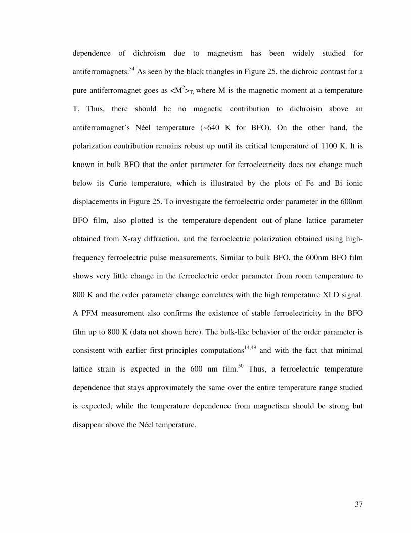
37
dependence of dichroism due to magnetism has been widely studied for
antiferromagnets.34
As seen by the black triangles in Figure 25, the dichroic contrast for a
pure antiferromagnet goes as <M2>T, where M is the magnetic moment at a temperature
T. Thus, there should be no magnetic contribution to dichroism above an
antiferromagnet’s Néel temperature (~640 K for BFO). On the other hand, the
polarization contribution remains robust up until its critical temperature of 1100 K. It is
known in bulk BFO that the order parameter for ferroelectricity does not change much
below its Curie temperature, which is illustrated by the plots of Fe and Bi ionic
displacements in Figure 25. To investigate the ferroelectric order parameter in the 600nm
BFO film, also plotted is the temperature-dependent out-of-plane lattice parameter
obtained from X-ray diffraction, and the ferroelectric polarization obtained using high-
frequency ferroelectric pulse measurements. Similar to bulk BFO, the 600nm BFO film
shows very little change in the ferroelectric order parameter from room temperature to
800 K and the order parameter change correlates with the high temperature XLD signal.
A PFM measurement also confirms the existence of stable ferroelectricity in the BFO
film up to 800 K (data not shown here). The bulk-like behavior of the order parameter is
consistent with earlier first-principles computations14,49
and with the fact that minimal
lattice strain is expected in the 600 nm film.50
Thus, a ferroelectric temperature
dependence that stays approximately the same over the entire temperature range studied
is expected, while the temperature dependence from magnetism should be strong but
disappear above the Néel temperature.

38
We see elements of both order parameters in the dichroic temperature dependence of
BFO. Figure 25 shows the measured results on five samples during both heating and
cooling. In all cases the PEEM images were captured from the same area of the BiFeO3
film after waiting thirty minutes at each temperature to allow thermal equilibration. The
data on one of the samples were recorded on an electrically switched area (see later
discussion) while the others were recorded
on un-switched areas. We see that in all
cases the linear dichroism signal drops
rapidly on heating above room temperature,
with only ~50% of the room-temperature
XLD value remaining at the Néel
temperature; this reduction is recovered on
cooling. We therefore conclude that the high
temperature XLD signal results from the
ferroelectric ordering, and the signal below
TN from the sum of the antiferromagnetic
and ferroelectric contributions. At room
temperature, the magnetic and ferroelectric
components are of roughly equal strength.
The dichroism images from section 3.2 are
not dominated by only ferroelectricity, but
instead a roughly equivalent combination of ferroelectricity and magnetism, which can be
separated through this angle and temperature dependent approach.
a) c)
b) d)
e)
Figure 26 - PEEM images before (a) and
after (b) poling. The arrows show the x-ray
polarization direction. In-plane PFM images
before (c) and after (d) poling. The arrows
show the direction of the in-plane component
of ferroelectric polarization. Regions 1 and 2
correspond to 109◦ ferroelectric switching,
whereas 3 and 4 correspond to 71◦ and 180◦
switching, respectively. (e) A superposition
of in-plane PFM scans shown in c and d used
to identify the different switching.

39
3.6 Magnetoelectric Coupling
Having conclusively shown that the PEEM images contain contributions from both order
parameters, we now return to the question of electric control of magnetism in BFO by
comparing PFM and PEEM images of an area that has been poled. Figures 26a-b show
our PEEM results for the BiFeO3 film before and after electrical poling, with the
corresponding in-plane PFM results shown in Figure 26c-d. The poled area is outlined by
dotted boxes in each figure. We know from the out-of-plane PFM images (not shown)
that ferroelectric polarization switches under the applied bias of −12 V. As discussed
before, to unambiguously identify the polarization direction in each domain, in-plane
PFM scans have been taken along two orthogonal [110] directions (only one shown here).
The different switching mechanisms are easily distinguished by superimposing the in-
plane PFM images taken before (the grayscale image) and after (the colored image)
electrical poling along the same direction, as shown in Figure 26e. The three possible
switching mechanisms appear with different colors as marked in Figure 26e. This image
serves as a guide to identifying regions that exhibit different switching mechanisms in
Figure 26a–d. For example, regions 1 and 2 correspond to 109◦ switching, region 3 to 71◦
switching, and region 4 to 180◦ switching. Both 71◦ and 180◦ ferroelectric switching do
not change the in-plane projection of the ferroelectric and antiferromagnetic order
parameters (Figures 21b and 21d), and thus cannot be detected by a PEEM setup with a
fixed x-ray polarization direction parallel to the sample surface. As a result, there is no
observable contrast change in regions 3 and 4, although switching may have occurred.
(Note that later discussion will show that the ferroelectric and antiferromagnetic coupling

40
in the 71◦ ferroelectric switching region can possibly exhibit a complicated behavior. The
PEEM results at least confirm that the in-plane projection of the antiferromagnetic axis is
not changed by the 71◦ ferroelectric switching.) The following discussion will focus on
the regions with 109◦ ferroelectric switching. As can be seen in Fig. 5, the PEEM images
from the same area track the changes in the PFM images in the region with 109◦
ferroelectric switching: the PEEM contrast reverses, either from bright to dark (region 1)
or vice versa (region 2), on ferroelectric switching. Finally, note that the dichroism value
(the difference in intensity between the dark and bright domains) and temperature
dependence are unchanged by the electrical switching, confirming that the
antiferromagnetic domains are switching with the ferroelectric domains; if the
ferroelectric polarization switched without reorienting the antiferromagnetic axis, then
the ferroelectric component of the XLD would change sign, whereas the
antiferromagnetic component would not. As a result, the dichroism value in the switched
area would have a smaller value and a different temperature dependence.
Pioneered by Ascher and co-workers on Boracite7 in 1960s, electric control of a
magnetic domain has been reported on several materials, such as YMnO3.51
The research
presented here, however, goes further than the earlier work in that it is (1) at room
temperature; (2) on thin films, a more favorable system for applications; and (3)
performed with an active control, unlike in the YMnO3 case.51
This is the first
observation of ferroelectrically-induced antiferromagnetic switching at room temperature.
Very recently, an exchange bias coupling between an antiferromagnetic BiFeO3 layer and
an adjacent ferromagnetic layer has been reported.52
By combining the ability to
41
ferroelectrically control antiferromagnetism (as revealed in this work) and the capabilities
of antiferromagnetic modulation of ferromagnetism,52
an ultimate electric control of
ferromagnetism can be achieved, as will be the topic of Chapter 6.
Recall that the first-principles calculation of the magnetocrystalline anisotropy in bulk
BiFeO3 predicted a six-fold degeneracy of the orientation of the antiferromagnetic
sublattice magnetization within the [111] plane.14
In such a case we would, in principle,
expect to see many different antiferromagnetic domains within each ferroelectric domain
with different projections of the antiferromagnetic order parameter on the polarization
direction of the x-ray beam. However, in the PEEM measurements it seems that every
ferroelectric domain coincides with only one antiferromagnetic domain. This could either
mean that the six-fold degeneracy is broken in the films so that only one possible
orientation of the antiferromagnetic axis with respect to the ferroelectric polarization
occurs, or that we see only an effective projection of the antiferromagnetic axis, averaged
over all six possible orientations because of the resolution limits of the PEEM. The six-
fold degeneracy could be lifted, for example, by a small monoclinic strain, which could
indeed occur in a BiFeO3 film grown on a (001) substrate; although the homogeneous
strain in the 600-nm-thick films used in our experiments seems to be fully relaxed, a
small inhomogeneous strain component could still persist. Furthermore, the degeneracy
of the magnetization direction could also be lifted by other effects related to the presence
of the surface and the substrate. The effect of strain and thickness and how they can be
utilized to control magnetism will be the focus of Chapter 5.

42
Figure 27 - Table of Bragg intensities for BFO
crystal before (top) and after (bottom) electric
field poling53
3.7 Confirmation
In the year following the publication of the
results presented in this chapter, the
coupling between ferroelectricity and
antiferromagnetism was confirmed for
single crystals of BFO using neutron
scattering measurements.53
The single
crystals grown by this group have only one
as-grown ferroelectric direction, as opposed
to the thin films discussed before. Due to the rhombohedral symmetry of the crystals,
there are three equivalent propagation vectors for the magnetism: k1 = [δ 0 -δ], k2 = [0 δ -
δ] and k3 = [-δ δ 0] where δ = 0.0045. The same experiment completed for powder
neutron diffraction would result in three different equally populated k domains, leading to
a splitting of magnetic peaks along the three directions. Lebeugle et. al. measured the
intensity distribution of the as-grown crystals around the four antiferromagnetic Bragg
reflections of the (½, ½, ½) type. The top table in Figure 27 illustrates that prior to
electric field poling all of the magnetic information lie along one direction (in bold),
namely k = [1 0 -1]. However, after electric field poling when roughly half of the
domains rotate by 71 degrees, the Bragg intensity becomes an average of the equivalent
k1 for the new polarization direction and the original k1. No other k value is selected (k2
or k3), demonstrating that the magnetic order is coupled to the ferroelectric order in BFO
crystals.
43
In this chapter, the existence of magnetoelectric coupling in BFO thin films was
explored. We learned that electric control can be achieved theoretically by manipulating
the magnetic plane perpendicular to the ferroelectric direction. By comparing PFM and
PEEM images at the same locations, this control was confirmed experimentally in BFO
thin films. Additionally, PEEM’s sensitivity to ferroelectricity as well as magnetism was
introduced and investigated through thorough temperature dependence. This electrical
control of magnetism in BFO crystals was confirmed by Lebeugle et. al. This study is an
excellent step in being able to manipulate magnetoelectric coupling; however, in order to
fully benefit from this cross-parameter control, a detailed understanding of the individual
order parameters and how they can be influenced is necessary. The ferroelectric
properties of BFO are already well studied.12
The full magnetic behavior as it varies with
thickness will be the topic of the next chapter.

44
Chapter 4: Thickness Dependence of Magnetism in BFO
This chapter starts with a continuation of the discussion of BFO crystals, focusing on the
details of the magnetic order. Significant differences in the polarization of thin films were
discovered, prompting the investigation of the effect of thickness on ferroelectric and
magnetic properties in BFO films. Angle- and temperature-dependent PEEM
measurements in addition to dichroism modeling were utilized to discover a preferred
magnetic [112]-type axis in thin films, as opposed to the easy magnetic plane observed in
bulk. Finally, the reduction of ferroelectric polarization and magnetic is addressed for
ultrathin BFO films.
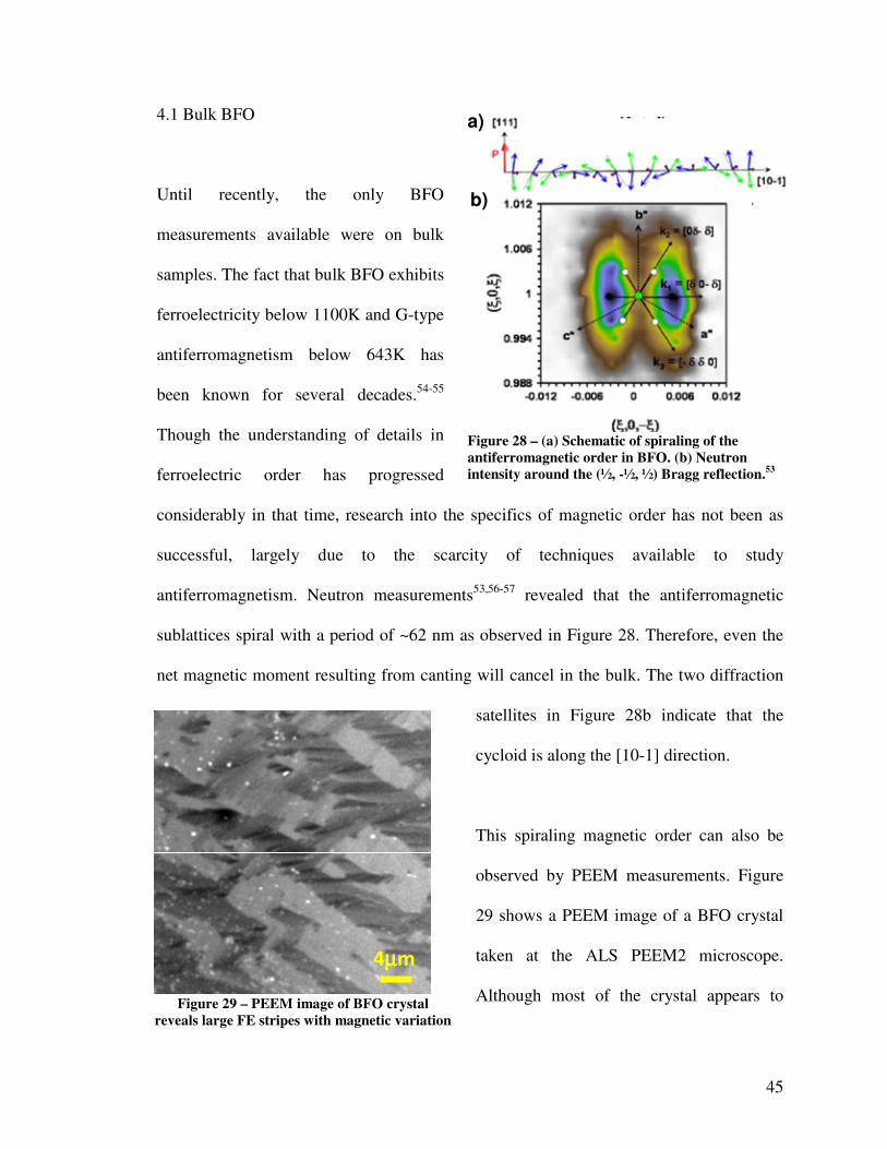
45
4.1 Bulk BFO
Until recently, the only BFO
measurements available were on bulk
samples. The fact that bulk BFO exhibits
ferroelectricity below 1100K and G-type
antiferromagnetism below 643K has
been known for several decades.54-55
Though the understanding of details in
ferroelectric order has progressed
considerably in that time, research into the specifics of magnetic order has not been as
successful, largely due to the scarcity of techniques available to study
antiferromagnetism. Neutron measurements53,56-57
revealed that the antiferromagnetic
sublattices spiral with a period of ~62 nm as observed in Figure 28. Therefore, even the
net magnetic moment resulting from canting will cancel in the bulk. The two diffraction
satellites in Figure 28b indicate that the
cycloid is along the [10-1] direction.
This spiraling magnetic order can also be
observed by PEEM measurements. Figure
29 shows a PEEM image of a BFO crystal
taken at the ALS PEEM2 microscope.
Although most of the crystal appears to
a)
b)
Figure 28 – (a) Schematic of spiraling of the
antiferromagnetic order in BFO. (b) Neutron
intensity around the (½, -½, ½) Bragg reflection.53
4µµµµm
Figure 29 – PEEM image of BFO crystal
reveals large FE stripes with magnetic variation

46
have only one ferroelectric domain, there are regions where two ferroelectric variants
with domain widths of several microns are observed. Within the stripe-like ferroelectric
domains, there is variation of contrast which is believed to be the spiraling of the
magnetic order. To verify this, the contrasts in the three boxes (B, C, and D) in Figure
30a were measured with the light polarization of the incident x-rays rotated from vertical
(s-polarized) to horizontal (p-polarized). The detail behind these changes in contrast will
be discussed in more detail for thin films later in this chapter, but some trends are already
evident. Even within the same ferroelectric domain (boxes B and D), there are different
angular dependencies (Figure 30b). Between ferroelectric domains, the difference is even
greater, which is expected since the magnetism lies on difference planes, perpendicular to
the two ferroelectric directions.
Spiraling magnetic order has an interesting consequence beyond the lack of net magnetic
moment. The linear magnetoelectric effect is averaged to zero in bulk BFO due to the fact
that the average value of the projection of the antiferromagnetic vector in the cycloidal
0 20 40 60 80 1002000
2020
2040
2060
2080
Inte
nsity
Light Polarization Rotation
B
C
D
a) b)
s p
4µµµµm
BD
C
(α)
Figure 30 – (a) PEEM image showing the location of three areas for x-ray light polarized at α= 0°°°°.
(b) The angular contrast of these areas are shown through the light polarization rotation.

47
structure is zero.58
Many believe that the linear magnetoelectric term—being the first
order term—must be present in order to have strong coupling. The cycloidal structure
does not prevent manifestation of the quadratic magnetoelectric effect.59
There is at least
one way to allow a linear effect: the spin cycloidal structure that prevents the linear
magnetoelectric effect from being observed can be destroyed by high magnetic field.60
Application of high magnetic field (~20 Tesla) can induce a phase transition from a
spatially-modulated spin structure to one with a homogeneous spin order.58
However, it
seems unlikely that such a high field would be useful for energy saving applications of
magnetoelectrics.
4.2 BFO Thin Films
4.2.1 Discovering Differences Between Thin and Thick Films
The lack of a linear magnetoelectric effect in bulk BFO led many to believe that strong
magnetoelectric coupling would not be possible for this material. Some researchers
decided to search for new materials despite the fact that no other room temperature
magnetic ferroelectric was known. Others looked for more exotic approaches, such as
interface magnetoelectricity by combining two or more materials, but they have met with
limited success so far. Most recently, new research on BFO has shown that it may still be
a viable candidate material for magnetoelectric coupling.

48
The Ramesh group discovered that
BFO thin films, though still
ferroelectric and antiferromagnetic,
possess important differences from
their sister crystals shown in Figure 31.
It was recently believed that the bulk
BFO spontaneous polarization Ps was
only 3.5 microcoulombs per square
centimeter (µC/cm2) along the (001)
direction, whereas BFO thin films
have a Ps of approximately 55 µC/cm2.61
Today, it is known that high-quality crystals and
films have the same large Ps, illustrating the importance of first-rate growth and
characterization to certify material excellence. This actual value is big enough to rival
some of the best known ferroelectrics such as PZT, making BFO an attractive alternative
for existing ferroelectric applications and allowing for new possible functions involving
both ferroelectricity and magnetism. Additionally, though no net magnetic moment had
been observed for BFO crystals, moments as large as 200 emu/cc have been measured in
films. Large angle x-ray scans of these thin films showed diffraction peaks from only the
substrate and the (001) pseudocubic reflections. No reflections indicated secondary
phases. Throughout this chapter three classes of films will be addressed: ultra-thin films
with thickness (t) < 20 nm, thin films that have 20 nm < t < 200 nm, and thick films that
have t ~1 µm.
Figure 31 – Recent understanding of ferroelectric
hysteresis curves for 200 nm thick BFO films and
crystals.

49
4.2.2 Exploring Reasons for Differences
Why should the properties of thin film BFO be significantly different from BFO crystals?
Jiang and Qui used the Landau free energy function—commonly used for
ferroelectrics—to investigate the ferroelectric and magnetic properties of epitaxial BFO
thin films.62
They found that the lattice parameter, polarization and magnetization of BFO
are theoretically a function of strain as plotted in Figure 32. In very thin films, the lattice
parameters of BFO attempt to match those of the substrate as long as the mismatch is not
too large (Figure 32a). However, as films grow in thickness, this matching relaxes and
eventually reaches bulk lattice parameters. Limited data fit relatively well to the theory,
though no ultrathin films (thickness < 25 nm) were compared in this study. Theory
suggests a large increase in the polarization and magnetization for small thicknesses. This
theory fits well with past observations on pure ferroelectrics which found that although
bulk ferroelectric oxides normally break long before they are strained to percent levels,
such strains are readily applied to ferroelectric thin films through the use of epitaxy on
appropriate substrates.63
These strains can have a tremendous effect on the properties of
ferroelectric thin films and superlattices. They can make materials that are not
ferroelectric at any temperature ferroelectric and also change the ordering temperature by
hundreds of degrees while simultaneously enhancing the remnant polarization.
a) b) c)
Figure 32 - Film thickness dependence of (a) c-axis lattice parameter, (b) spontaneous polarization
P0, and (c) saturation magnetization Msat with the saturated magnetic field of 6000 Oe.
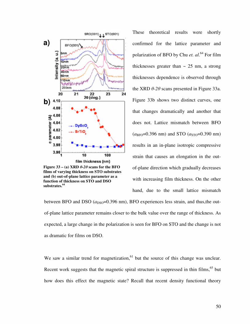
50
These theoretical results were shortly
confirmed for the lattice parameter and
polarization of BFO by Chu et. al.64
For film
thicknesses greater than ~ 25 nm, a strong
thicknesses dependence is observed through
the XRD θ-2θ scans presented in Figure 33a.
Figure 33b shows two distinct curves, one
that changes dramatically and another that
does not. Lattice mismatch between BFO
(aBFO=0.396 nm) and STO (aSTO=0.390 nm)
results in an in-plane isotropic compressive
strain that causes an elongation in the out-
of-plane direction which gradually decreases
with increasing film thickness. On the other
hand, due to the small lattice mismatch
between BFO and DSO (aDSO=0.396 nm), BFO experiences less strain, and thus,the out-
of-plane lattice parameter remains closer to the bulk value over the range of thickness. As
expected, a large change in the polarization is seen for BFO on STO and the change is not
as dramatic for films on DSO.
We saw a similar trend for magnetization,61
but the source of this change was unclear.
Recent work suggests that the magnetic spiral structure is suppressed in thin films,65
but
how does this effect the magnetic state? Recall that recent density functional theory
a)
b)
Figure 33 – (a) XRD θ-2θ scans for the BFO
films of varying thickness on STO substrates
and (b) out-of-plane lattice parameter as a
function of thickness on STO and DSO
substrates.64

51
calculations for bulk BFO predict that the
individual moments for each Fe-ion should
lie along any one of six possible
energetically-degenerate magnetic axes of
the <1-10>- or <112>-type in an easy 111-
type plane, which are perpendicular to the
<111> polarization direction,14
shown as
the transparent red plane in Figure 34. This degeneracy of the magnetic axes is lifted if
BFO becomes monoclinic, as would occur due to strains caused by growing on a
substrate. The strain squeezes the 111 plane horizontally and allows it to stretch
vertically.
Why should this stretching and squeezing affect the magnetic behavior of BFO?
Antiferromagnetism in BFO comes from superexchange mediated through the Fe-O-Fe
bonds. The exchange constant is thought to depend strongly on distance, and therefore
these small changes might have a drastic effect.66
This choice of a preferred axis is not
unheard of in other materials; strain-driven changes in magnetic structure have been
observed previously in other magnetic oxide systems which exhibit a strong coupling
among spin, charge, orbital and lattice degrees of freedom (for example, refs. 41 and 66).
In these materials, strain-induced changes have been interpreted by considering the
variation of the electronic hopping amplitude due to the change of bond lengths and bond
angles.66
Strain has been shown to affect the nature of antiferromagnetism in oxides such
as NiO. It has been suggested that an orthorhombic contraction (i.e., that which would
<111>
-110
-211
-101
-12-1
01-111-2
xy
z
Bi Fe O
FEFEFEFE
Figure 34 – Schematic showing six energetically
preferred axes for BFO with ferroelectric
polarization pointing along [111].

52
result from an in-plane compressive strain) along [100] favors a <110> easy axis,
whereas a monoclinic expansion (i.e., that which would result from an in-plane tensile
strain) along [110] favors a <112> easy axis.67
Recall that the lattice mismatch between BFO and STO (1.54%) imparts a compressive
in-plane strain to the BFO film that is progressively relaxed as the film thickness is
increased.64
Using x-ray reciprocal space mapping (RSM) of the 203 BFO diffraction
peak as shown in Figure 35a-b we have studied the strain state in such films as a function
of film thickness. The in-plane (a) and out-of-plane (c) lattice parameters, as well as the
monoclinic tilt angle (β), are shown in the table, along with a schematic describing the
a
b[001]o
[11
0] o
[001]o
[11
0] o
βa δ
c
βa δ
cc
c)
d)
BFO 203
STOSRO
STO
BFO 203
200 nm
1.0 µm
a=3.909 Å (-1.43%)
c=4.062 Å (+2.44%)
ββββ = 0.65°°°°
a=3.954 Å (-0.28%)
c=3.975 Å (+0.24%)
β β β β = 0.74°°°°
Th
inT
hic
k
4.9
4.8
4.7
4.6
4.9
4.8
4.7q(Å
-1)
┴
3.1 3.2 3.3
q(Å
-1)
┴
q║(Å-1)
a)
b)
Figure 35 - The crystal structure of thin and thick BFO films grown on SRO/STO(001). RSMs
for thin (a) and thick (b) BFO grown on SRO/STO(001). (c) Schematic illustrating the nature of
the crystal structure of the BFO film, where a is the in-plane lattice parameter, c is the out-of-
plane lattice parameter, and β is the monoclinic distortion angle. (d) Unit cell parameters, as
determined by RSM, for both strained (thin) and relaxed (thick) films.
53
nature of the structural distortions (Figures 35c and 35d). In the case of a 200 nm thick
BFO/SRO/STO (001) film, the in-plane lattice parameters are matched with those of the
substrate and the unit cell is under compressive strain (c/a-1 ~ +3.9%) [Figure 35a]. As
the film thickness is increased to 1 µm, the lattice parameters gradually approach the bulk
BFO value and the pseudo-tetragonality (c/a-1) becomes smaller (+0.53%) as measured
from RSM (Figure 35b). β is derived from the peak splitting of the 203-peak and is
calculated to be ~0.74°, close to the value measured in bulk BFO. The in-plane
compressive strain lifts the degeneracy of magnetization in the 111-plane, as is also
observed in the case of NiO thin films.41
A preferred axis can also be understood in terms
of the magnetostriction in BFO. The magnetostriction constant of BFO is positive,68
meaning that the lattice constants expand along an applied magnetic field. Substrate-
induced compressive strain is effectively the opposite of this effect and thus results in a
preference of a magnetization direction that has the largest out-of-plane component while
remaining in the (11-1), i.e, the <112>. However, another argument claimed that the 110
axis, which is in-plane, would be preferred because it can be shared by four different
polarization directions and that would be efficient energetically.47
To determine between
these axes and other possible magnetic behaviors, we used angle-resolved, temperature-
dependent PEEM measurements compared with ferroelectric PFM measurements.69

54
4.2.3 Angle-Dependent Measurements of BFO Thin Films
Single phase, epitaxial thin films of BFO were grown on a 50 nm thick conductive
bottom electrode of SrRuO3 (SRO) on SrTiO3 (STO) (001) single crystal substrate via
laser-molecular beam epitaxy and metalorganic chemical vapor deposition. Detailed x-
ray diffraction studies coupled with transmission electron microscopy were used to
establish the crystalline quality of the heterostructures; these films were found to be
single phase and fully epitaxial.
As measured by PFM discussed previously, the in-
plane ferroelectric domain structure of one BFO
thin film is shown in Figure 36. The long axis of the
ferroelectric domains (or direction of the domain
walls) lies along the <100> of the underlying
SrTiO3 (001) substrate or the pseudocubic-<100> of
BFO. The polarization direction of the various
stripe-like domains lies along the <111> and the in-
plane projection of those polarization directions lies
along the <110>. The arrows in Figure 36 refer to the in-plane projection of the
ferroelectric polarization directions (four variants) present in this model system. Such a
model ferroelectric domain structure forms the reference frame for our photoemission
measurements.
s
p
BFO [110]
x-rays
30°°°°
BFO [-110]
2 4 6 8
cantilever
µµµµm
Figure 36 - PFM image of in-plane
polarization projections with PFM and
PEEM geometries (taken separately),
showing incident x-rays 30 degrees from
sample surface.

55
Once the ferroelectric domains are well characterized, the magnetic behavior can be
studied. L-edge spectra depend on anisotropies in the charge or the spin in the material,
and thus are sensitive to the relative orientation of the x-ray polarization and AFM axes
which are then imaged by PEEM. Recognizing that x-ray linear dichroism can arise from
any anisotropic distribution of charge in a material, (as discussed in sections 3.4 and 3.5
for the case of both ferroelectric and antiferromagnetic order), we have decoupled the
contributions from these sources
unambiguously through temperature- and
angle-dependent measurements.
Figure 37a illustrates the x-ray polarization
geometry in which the XLD-PEEM images in
Figures 37b-e were taken. The images in
Figures 37b-e are from the corresponding area
shown in Fig.36 (the “T” shape in Figures 36
and 37b are outlined as an aid to the reader).
Images result from dividing intensity maps
taken at the Fe-L3 absorption edge using
linearly polarized light as the angle of the
plane of linear incident polarization (α) varies
from 0° (p polarization) to 90° (s
polarization). The outlined arrows in Figure
37 show the in-plane projection of the four
α = 0°
α = 70°
α = 40°
Eα = 90°
b) c)
d) e)
4 1
3 2
4 1
3 2
4 1
3 2
4 1
3 2
a)
100
1 µµµµm
Figure 37 - PEEM images of BFO at several
angles of the electric vector of incident linear
polarization α. (a) Schematic illustrating the
experimental geometries used to probe the
angle dependent linear dichroism in BFO. The
outlined arrows show the in-plane projection
of the four ferroelectric directions. Images of
domain structures taken at (b) α=90°, (c)
α=70°, (d) α=40°, and (e) α=0°.

56
ferroelectric directions. When the x-rays are s-polarized (α = 90°), only two contrast
scales [labeled as light (1 and 3) and dark (2 and 4) in Figure 37b] are observed. We have
chosen a geometry such that the x-ray polarization vector for an s-polarized incident
beam is along [-110], which maximizes the difference in intensity between the domains.
In this geometry, the propagation vector of the incident x-rays is nearly parallel to [1 1 -
1], as shown in 37a, due to the θ = 30° grazing angle from the sample surface. Figures
37b-e were obtained by changing the x-ray polarization angle α and keeping the grazing
incidence angle θ fixed, which allowed us to gain insight into the magnetic structure by
plotting the α-angle dependence of the x-ray dichroic signal. Individual ferroelectric
directions can be preferentially identified by rotating the polarization relative to the
crystal as demonstrated in Figure 37c. For example, in this figure, the technique
highlights all [-1 1 -1]-type ferroelectric domains (black arrow). The angle dependence
reveals that at α = 70°, three of the four <1 1 1> type domains have similar contrast while
the intensity from [-1 1 -1] domains is much higher. Further rotation of the polarization to
α = 40° (Figure 37d) results in an image where all four ferroelectric variants can be
distinguished due to their differences in contrast. Contrast between certain domain types
can also vanish at other x-ray polarization angles, such as the [1-1-1] and [-11-1]-type
domains in Figure 37e for α = 0.
Focusing on the image in Figure 37c where we have controlled the relative orientation of
the incidence x-ray polarization and the crystallographic orientation of BFO to
preferentially observe one ferroelectric direction (in this case all ferroelectric domains of
the [-11-1]-type), we gain insight into the nature of magnetism in BFO. We note again
57
that all individual domains of a specific ferroelectric direction exhibit identical contrast.
This indicates that the antiferromagnetic order in a given set of identical ferroelectric
domains is the same, and automatically rules out the possibility of a magnetic structure
such as that in a bulk sample of BFO in which there is a 111-type easy plane of
magnetization perpendicular to the polarization direction. PEEM imaging in this
geometry would result in multiple contrast levels for a given set of identical ferroelectric
domains if the antiferromagnetic domains were larger then the PEEM resolution (~30
nm). The formation of antiferromagnetic domains with sizes smaller than 30 nm is
highly unlikely, purely due to energetic considerations.70
Therefore, the data in Figure
37c is consistent with a magnetic structure in which an easy magnetic axis is formed in
the {111}-magnetization plane of BFO, similar to what is observed in strained NiO
films.41
4.2.4 Modeling Expected Domain Contrast
Simple models of the x-ray polarization angle (α) dependence of the dichroic domain
contrast further support this conclusion. From a series of images (such as those in Fig.
37b-e), we can extract the α dependence of dichroic contrast (from both ferroelectric and
magnetic contributions) for thin and thick films and compare this data to model
calculations as a function of the x-ray polarization angle α. The angle dependence of the
magnetic contribution to linear dichroism of an antiferromagnet has been modeled36
previously as
I = (3cos2ӨM – 1) <M
2>T (5)
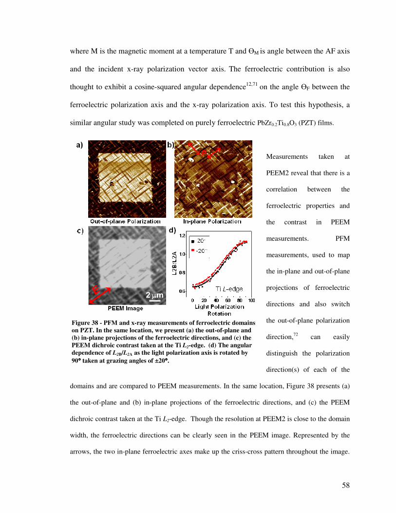
58
where M is the magnetic moment at a temperature T and ӨM is angle between the AF axis
and the incident x-ray polarization vector axis. The ferroelectric contribution is also
thought to exhibit a cosine-squared angular dependence12,71
on the angle ӨF between the
ferroelectric polarization axis and the x-ray polarization axis. To test this hypothesis, a
similar angular study was completed on purely ferroelectric PbZr0.2Ti0.8O3 (PZT) films.
Measurements taken at
PEEM2 reveal that there is a
correlation between the
ferroelectric properties and
the contrast in PEEM
measurements. PFM
measurements, used to map
the in-plane and out-of-plane
projections of ferroelectric
directions and also switch
the out-of-plane polarization
direction,72
can easily
distinguish the polarization
direction(s) of each of the
domains and are compared to PEEM measurements. In the same location, Figure 38 presents (a)
the out-of-plane and (b) in-plane projections of the ferroelectric directions, and (c) the PEEM
dichroic contrast taken at the Ti L2-edge. Though the resolution at PEEM2 is close to the domain
width, the ferroelectric directions can be clearly seen in the PEEM image. Represented by the
arrows, the two in-plane ferroelectric axes make up the criss-cross pattern throughout the image.
Figure 38 - PFM and x-ray measurements of ferroelectric domains
on PZT. In the same location, we present (a) the out-of-plane and
(b) in-plane projections of the ferroelectric directions, and (c) the
PEEM dichroic contrast taken at the Ti L2-edge. (d) The angular
dependence of L2B/L2A as the light polarization axis is rotated by
90°°°° taken at grazing angles of ±20°°°°.

59
There is also an out of plane polarization direction, best observed in Figure 38a. The out-of-plane
ferroelectric direction (out of the plane or into the plane) can be controlled by application of an
electric field via PFM, as was completed inside the bright box in Figure 38a in order to establish
the sensitivity of dichroism to out-of-plane components as well as in-plane components. Now that
this ferroelectric contribution is established with this example and other comparisions,48
it is
important to know the angular dependence of this contribution so that we can incorporate it into
our dichroism model. Figure 38d shows the angular dependence of L2B/L2A as the light
polarization axis is rotated by 90 degrees (between s- and p-polarized light). The two curves
demonstrate that the same angular dependence is observed when the angle between the sample
and incident light is 20 degrees on the two opposite sides of the sample surface, as would be
expected if this is a ferroelectric effect due to having equivalent projections. The resulting angular
behavior can be modeled by a cosine squared relation, suggesting that the ferroelectric behavior
result in angular dependencies in dichroism similar to those observed due to magnetic properties.
Given this behavior, we have modeled the dichroism from a multiferroic material with
both magnetic and ferroelectric order when linearly polarized light is incident upon the
sample at a given temperature as
IXLD=P cos2ӨF + Q cos
2ӨM, (6)
where |P|+|Q|=1. Constants P and Q can be either positive or negative, where |P| and |Q|
are, respectively, the percentage contribution of the polarization and magnetic
components to the dichroism at the given temperature. We have considered both positive
and negative values for the constants P and Q in the current study. The dashed lines in
Figure 39a correspond to the selected images in Figure 37 and the colors of the curves
match the in-plane projection of the ferroelectric directions and colored arrows displayed
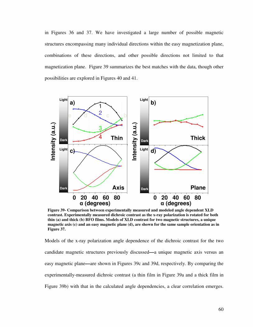
60
in Figures 36 and 37. We have investigated a large number of possible magnetic
structures encompassing many individual directions within the easy magnetization plane,
combinations of these directions, and other possible directions not limited to that
magnetization plane. Figure 39 summarizes the best matches with the data, though other
possibilities are explored in Figures 40 and 41.
Models of the x-ray polarization angle dependence of the dichroic contrast for the two
candidate magnetic structures previously discussed—a unique magnetic axis versus an
easy magnetic plane—are shown in Figures 39c and 39d, respectively. By comparing the
experimentally-measured dichroic contrast (a thin film in Figure 39a and a thick film in
Figure 39b) with that in the calculated angle dependencies, a clear correlation emerges.
Axis Plane
Thin Thick
b)
c) d)
a)
Inte
nsi
ty (
a.u
.)
0 20 40 60 80
Inte
nsi
ty (
a.u
.)
α (degrees)0 20 40 60 80 α (degrees)
e d c b
12
3
4
Light Light
Light Light
Dark Dark
Dark Dark
Figure 39- Comparison between experimentally measured and modeled angle dependent XLD
contrast. Experimentally measured dichroic contrast as the x-ray polarization is rotated for both
thin (a) and thick (b) BFO films. Models of XLD contrast for two magnetic structures, a unique
magnetic axis (c) and an easy magnetic plane (d), are shown for the same sample orientation as in
Figure 37.
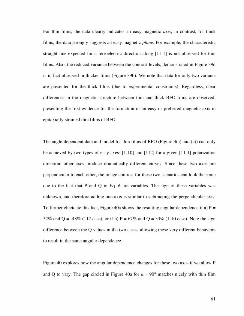
61
For thin films, the data clearly indicates an easy magnetic axis; in contrast, for thick
films, the data strongly suggests an easy magnetic plane. For example, the characteristic
straight line expected for a ferroelectric direction along [11-1] is not observed for thin
films. Also, the reduced variance between the contrast levels, demonstrated in Figure 39d
is in fact observed in thicker films (Figure 39b). We note that data for only two variants
are presented for the thick films (due to experimental constraints). Regardless, clear
differences in the magnetic structure between thin and thick BFO films are observed,
presenting the first evidence for the formation of an easy or preferred magnetic axis in
epitaxially-strained thin films of BFO.
The angle-dependent data and model for thin films of BFO (Figure 3(a) and (c)) can only
be achieved by two types of easy axes: [1-10] and [112] for a given [11-1]-polarization
direction; other axes produce dramatically different curves. Since these two axes are
perpendicular to each other, the image contrast for these two scenarios can look the same
due to the fact that P and Q in Eq. 6 are variables. The sign of these variables was
unknown, and therefore adding one axis is similar to subtracting the perpendicular axis.
To further elucidate this fact, Figure 40a shows the resulting angular dependence if a) P =
52% and Q = -48% (112 case), or if b) P = 67% and Q = 33% (1-10 case). Note the sign
difference between the Q values in the two cases, allowing these very different behaviors
to result in the same angular dependence.
Figure 40 explores how the angular dependence changes for these two axes if we allow P
and Q to vary. The gap circled in Figure 40a for α = 90° matches nicely with thin film

62
data (Figure 37a). However, as the P value is lowered for both axes (Figure 40b), this gap
disappears, which does not fit the observed dependence for any thickness of BFO. As P is
lowered further, this gap actually reverses as seen in Figure 40c. The act of increasing P
(instead of lowering it) results in an enlargement of the gap (Figure 40d), which is also
not found. It is clear that there is only a narrow range of P values that agree with the
angular dependence and this range is consistent with prior data.
Previous temperature-dependent measurements (discussed in Chapter 3) have shown that
the percentage of the dichroism at room temperature originating from the ferroelectric
polarization (P) is approximately 60 ± 10%.47
Unfortunately, the curves that best match
the observed angular dependence result from one of two cases (P112=.52 or P1-10=.67) that
are within the experimental error. In order to uniquely identify this axis, we have carried
out a unique set of temperature-dependent measurements.
20 40 60 80
0.1
0.2
0.3
0.4
0.5
0.6
20 40 60 80
0.1
0.2
0.3
0.4
0.5
20 40 60 80
0.1
0.2
0.3
0.4
0.5
0.6
0.7
20 40 60 80
0.1
0.2
0.3
0.4
0.5
P1-10=.67P112=.52
Light
Dark
Inte
nsi
ty (
a.u
.)
Inte
nsi
ty (
a.u
.)
Dark
Light
0 20 40 60 80 α (degrees)
0 20 40 60 80 α (degrees)
P1-10=.57P112=.34
P1-10=.52P112=.05
P1-10=.77P112=.67
b)
c) d)
a)
Figure 40 – The effect of the P values on the expected angular dependence of PEEM contrast for
two possible magnetic axes: [1-10] (black) and [112] (red). The same curves are obtained for two
different P values when the opposite magnetic axis is considered.
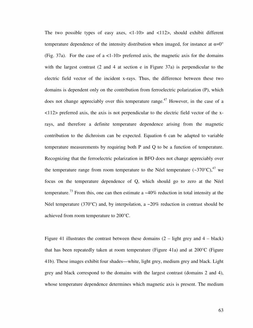
63
The two possible types of easy axes, <1-10> and <112>, should exhibit different
temperature dependence of the intensity distribution when imaged, for instance at α=0°
(Fig. 37a). For the case of a <1-10> preferred axis, the magnetic axis for the domains
with the largest contrast (2 and 4 at section e in Figure 37a) is perpendicular to the
electric field vector of the incident x-rays. Thus, the difference between these two
domains is dependent only on the contribution from ferroelectric polarization (P), which
does not change appreciably over this temperature range.47
However, in the case of a
<112> preferred axis, the axis is not perpendicular to the electric field vector of the x-
rays, and therefore a definite temperature dependence arising from the magnetic
contribution to the dichroism can be expected. Equation 6 can be adapted to variable
temperature measurements by requiring both P and Q to be a function of temperature.
Recognizing that the ferroelectric polarization in BFO does not change appreciably over
the temperature range from room temperature to the Néel temperature (~370°C),47
we
focus on the temperature dependence of Q, which should go to zero at the Néel
temperature.73
From this, one can then estimate a ~40% reduction in total intensity at the
Néel temperature (370°C) and, by interpolation, a ~20% reduction in contrast should be
achieved from room temperature to 200°C.
Figure 41 illustrates the contrast between these domains (2 – light grey and 4 – black)
that has been repeatedly taken at room temperature (Figure 41a) and at 200°C (Figure
41b). These images exhibit four shades—white, light grey, medium grey and black. Light
grey and black correspond to the domains with the largest contrast (domains 2 and 4),
whose temperature dependence determines which magnetic axis is present. The medium

64
grey is achieved for both 1 and 3 domains. As
illustrated by the several 2/4 locations plotted in
Figure 41c, the contrast was found to decrease by
~17% upon heating, which is in reasonable
agreement with the <112> easy axis scenario.
Continued contrast reduction was observed at
higher temperatures, but sample damage at these
temperatures began to threaten sample integrity
and therefore data beyond 200°C has not been
included. Measurements have been completed on
a blank BFO film and also on films capped with a
2 nm thick layer of SRO pre-heated for one hour
at 200°C in an attempt to minimize the impact of
any surface chemistry effects. The same trend
expected for the <112> case was observed in all
cases.
Both angle- and temperature-dependent PEEM
measurements support the case for a preferred
[112] magnetic axis for BFO thin films grown on STO substrates, where a strain of ~1%
exists. BFO films of thickness ~200 nm instead show magnetic behavior consistent with
the magnetic plane observed in BFO single crystals. This change with thickness is not
observed in BFO films grown on DSO, where the lattice mismatch is very small. The
a) 300K
500 nm
a) 300K
500 nm
b) 475Kb) 475K
3900
3600
3300
3000
Inte
nsity (
a.u
.)
Dark
Bright
Dark
Brightc)
300 400 500Temperature (K)
Figure 41 - Temperature dependent
dichroism measurements of BFO. XLD
images taken at (a) room temperature and
(b) 200°C. The labeled spots in (a) and (b)
represent a selection of locations used to
probe the temperature dependent change in
dichoric contrast. (c) Temperature
dependent changes in intensity for type 2
and 4 domains for both temperatures reveals
that the difference between the contrast
from type 2 and 4 domains reduces by 17%
at 200°C. This is expected for the presence
of a preferred magnetic [112] axis.
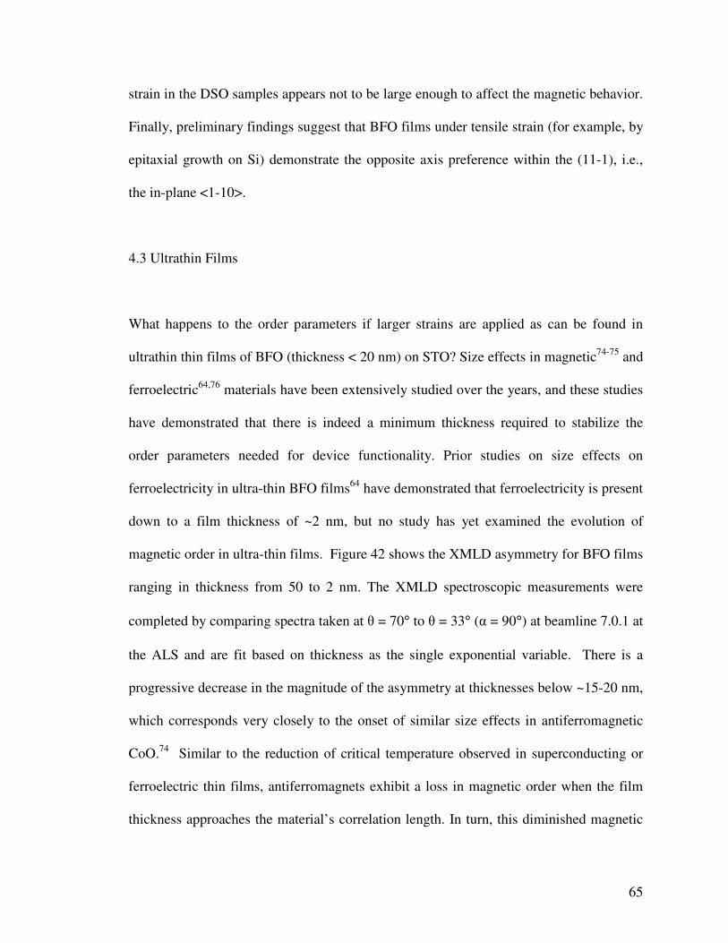
65
strain in the DSO samples appears not to be large enough to affect the magnetic behavior.
Finally, preliminary findings suggest that BFO films under tensile strain (for example, by
epitaxial growth on Si) demonstrate the opposite axis preference within the (11-1), i.e.,
the in-plane <1-10>.
4.3 Ultrathin Films
What happens to the order parameters if larger strains are applied as can be found in
ultrathin thin films of BFO (thickness < 20 nm) on STO? Size effects in magnetic74-75
and
ferroelectric64,76
materials have been extensively studied over the years, and these studies
have demonstrated that there is indeed a minimum thickness required to stabilize the
order parameters needed for device functionality. Prior studies on size effects on
ferroelectricity in ultra-thin BFO films64
have demonstrated that ferroelectricity is present
down to a film thickness of ~2 nm, but no study has yet examined the evolution of
magnetic order in ultra-thin films. Figure 42 shows the XMLD asymmetry for BFO films
ranging in thickness from 50 to 2 nm. The XMLD spectroscopic measurements were
completed by comparing spectra taken at θ = 70° to θ = 33° (α = 90°) at beamline 7.0.1 at
the ALS and are fit based on thickness as the single exponential variable. There is a
progressive decrease in the magnitude of the asymmetry at thicknesses below ~15-20 nm,
which corresponds very closely to the onset of similar size effects in antiferromagnetic
CoO.74
Similar to the reduction of critical temperature observed in superconducting or
ferroelectric thin films, antiferromagnets exhibit a loss in magnetic order when the film
thickness approaches the material’s correlation length. In turn, this diminished magnetic
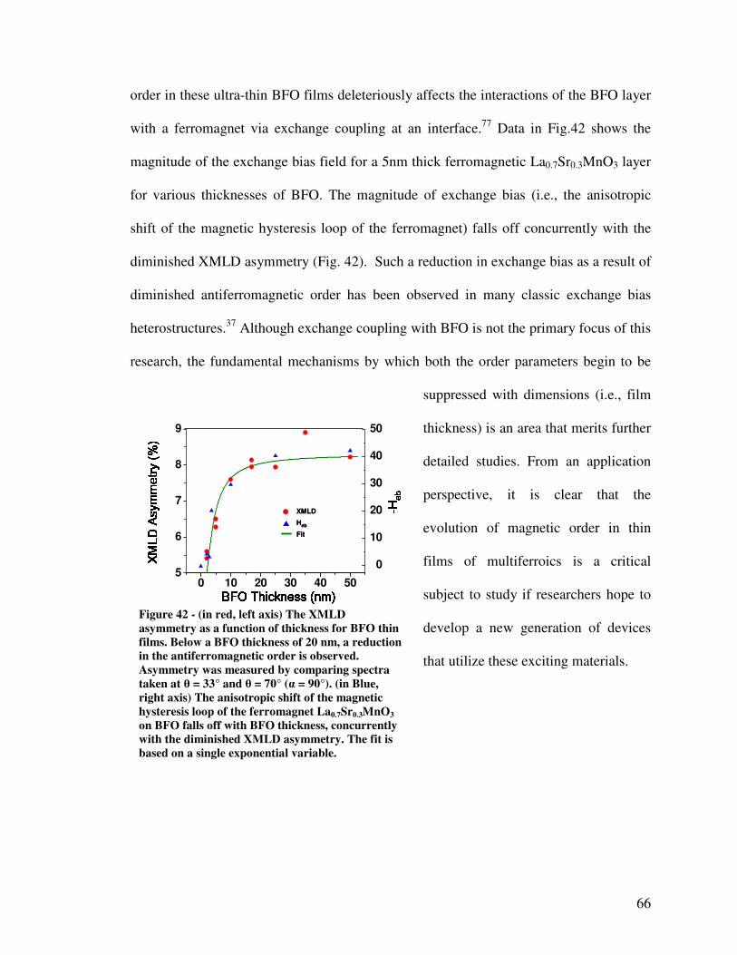
66
order in these ultra-thin BFO films deleteriously affects the interactions of the BFO layer
with a ferromagnet via exchange coupling at an interface.77
Data in Fig.42 shows the
magnitude of the exchange bias field for a 5nm thick ferromagnetic La0.7Sr0.3MnO3 layer
for various thicknesses of BFO. The magnitude of exchange bias (i.e., the anisotropic
shift of the magnetic hysteresis loop of the ferromagnet) falls off concurrently with the
diminished XMLD asymmetry (Fig. 42). Such a reduction in exchange bias as a result of
diminished antiferromagnetic order has been observed in many classic exchange bias
heterostructures.37
Although exchange coupling with BFO is not the primary focus of this
research, the fundamental mechanisms by which both the order parameters begin to be
suppressed with dimensions (i.e., film
thickness) is an area that merits further
detailed studies. From an application
perspective, it is clear that the
evolution of magnetic order in thin
films of multiferroics is a critical
subject to study if researchers hope to
develop a new generation of devices
that utilize these exciting materials.
0 10 20 30 40 505
6
7
8
9
0
10
20
30
40
50
BFO Thickness (nm)BFO Thickness (nm)BFO Thickness (nm)BFO Thickness (nm)----HHHHebebebebXMLD Asymm
etry (%)XMLD Asymmetry (%)XMLD Asymmetry (%)XMLD Asymmetry (%)
XMLD
Heb
Fit
XMLD
Heb
Fit
Figure 42 - (in red, left axis) The XMLD
asymmetry as a function of thickness for BFO thin
films. Below a BFO thickness of 20 nm, a reduction
in the antiferromagnetic order is observed.
Asymmetry was measured by comparing spectra
taken at θ = 33° and θ = 70° (α = 90°). (in Blue,
right axis) The anisotropic shift of the magnetic
hysteresis loop of the ferromagnet La0.7Sr0.3MnO3
on BFO falls off with BFO thickness, concurrently
with the diminished XMLD asymmetry. The fit is
based on a single exponential variable.

67
4.4 Summary of BFO Thickness Effects
The evolution of magnetism in BFO films discussed in this chapter is qualitatively
summarized by the PEEM images of five BFO samples of different thicknesses (22 nm to
bulk crystal) in Figure 43. The domain pattern changes quite considerably over this range
of thicknesses. In the crystal, we see very large ferroelectric domains with variation
within the domains, suggesting a rotation between axes consistent with the easy plane
case. To my knowledge, this is the first PEEM image of a BFO crystal, likely due to the
difficulty in obtaining a clear image when the surface is rough. As we reduce the
thickness of BFO, this easy plane simplifies into a preferred axis, resulting in a strong
magnetic anisotropy along that direction. Finally, at some ultrathin thickness, BFO starts
to lose its antiferromagnetism. This progression demonstrates that use of both strain
(controlled by film thickness and substrate choice) and electric field (discussed in
Chapter 3) to control the magnetic directions and strength of BFO which will be vital for
device design as illustrated in Figure 44.
1 0 1 0 0 1 0 0 0
BFO Thickness (nm)
AF
M O
rde
r P
ara
me
ter
Crystal
Preferred Axis
???
2µm2µm 2µm2µm 1µm1µm 4µm4µm2µm2µm
Easy Plane
Figure 43 – Evolution of BFO magnetism. PEEM images of 5 representative samples of a variety
of thicknesses are shown. The green line qualitatively describes the change in the magnetic order.

68
PPPP
<111>
-211
-101
-12-1
01-111-2
x
z
Bi
Fe O
PPPP
<111>
-211
-101
-12-1
01-111-2
x
z
Bi
Fe O
Strain
Ferroelectric
Antiferromagnet
-110
Figure 44 – Schematic illustrating that the antiferromagnetic properties of BFO(001) films can be
controlled through both strain and the electric field control of the ferroelectric domains.

69
Chapter 5: Orientation Influences on Magnetic Order
This chapter introduces the influence of film orientation on the magnetic properties in
BFO thin films. 110 and 111 orientations are introduced as alternatives to the 001
structure discussed throughout the rest of the thesis. The differences in the ferroelectric
nature for each orientation are presented. XAS and PEEM are utilized to determine the
magnetic behavior in the 110 and 111 orientations of BFO. Finally, the differences
between the three orientations are summarized.

70
5.1 Comparison of Ferroelectricity in BFO Orientations
The previous chapter discussed the in-depth understanding of the magnetic behavior of
BFO(001) films. This particular orientation of BFO was selected due to the several
ferroelectric directions present in these films as shown by the unit cell schematic and IP
PFM image in Figure 45a. By control of growth parameters presented in Appendix A, the
number of ferroelectric directions present in the BFO(001) film can be selected; one can
choose to create a sample having all 8 ferroelectric body diagonal directions, the four
downward pointing directions, only two, or a monodomain sample. Though the presence
of multiple ferroelectric directions in BFO(001) films was ideal for distinguishing the
magnetic behavior, one could argue that fewer directions would be more ideal for most
engineering applications. Now that several critical parameters in the 001 case have been
determined, such as the sign and magnitude of the p value in the multiferroic dichroism
formula, this knowledge can be applied to the study of other orientations of BFO.
6x6 µm26x6 µm2 10x10 µm2
(a) (b) (c)
(110)plane
PPPP1111---- PPPP
2222----
[1-10]
(111)plane
[100]
PPPP4444----
PPPP2222----
PPPP3333----
PPPP1111----
[-110]
[010]
PPPP4444----
PPPP2222----
PPPP3333----
PPPP1111----
[-110]
[010]
[001]
111110001
Figure 45 – Schematic and IP images of (a) 001, (b) 110, and (c) 111 orientations of BFO films.

71
110 and 111 orientations as well as their IP PFM images are shown in Figure 45b and c
respectively. BFO(110) typically results in two ferroelectric directions. The percentage of
each type of domain (from zero to one hundred percent) can be roughly selected based on
growth parameters. BFO(111) is a monodomain sample with the ferroelectric direction
pointing straight into the surface of the film. This OOP orientation is ideal for some
device architectures.
5.2 Magnetism in 110 BFO films
Let us now investigate the case of the 110 orientation of BFO in greater detail. As for
BFO(001) films, high-quality epitaxial BiFeO3(110) thin films were grown via PLD on
a) b)
c)
Figure 46 – BFO(110): IP PFM image of two ferroelectric domains (a) along with polarization
and antiferromagnetic direction schematics (b) and projections onto the 110 surface (c).

72
SrTiO3 substrates with a 50-nm-thick conducting SrRuO3 bottom electrode and the
resulting ferroelectric domain structures were studied by PFM. As illustrated in the in-
plane PFM image in Figure 46a, films were controlled to have two ferroelectric directions
of approximately equal volume fractions. The antiferromagnetic plane corresponding to
one of the two polarization variants is schematically illustrated in Figure 46b. In Figure
46c, the projections of ferroelectric polarization directions (red and grey arrows) and their
corresponding projections of the six degenerate directions in the antiferromagnetic (111)
plane (dotted lines) are shown in the same figure.
The influence of strain is again studied through the systematic control of the thickness of
BFO films, thereby manipulating lattice mismatch induced heteroepitaxial strain. Thin
films of thicknesses varying from a few nm to several microns were prepared by both
pulsed laser deposition and chemical vapor deposition. We specifically focused on two
representative thicknesses, namely 120 nm (thin) and 800 nm (thick) for our
photoemission experiments. The strain state of BiFeO3 thin films was analyzed by using
detailed four-circle x-ray diffraction measurements. Reciprocal space maps (RSM’s)78
were obtained around the (221) and (310) peaks for both samples The results of these
scans are shown in Figure 47a-d. The black dashed lines in the RSMs are guides to
identify the position of the reflection from the substrate. From these maps, we have
extracted the lattice parameters for the BFO unit cell in both cases. The schematic
diagram of the strained pseudo-cubic unit cells are presented in Figure 47e for the 120
nm film and in Figure 47f for the 800 nm film. Cyan rectangles represent the (110) plane
of STO. To describe the strain states quantitatively, a monoclinic unit cell is introduced

73
whose lattice parameters (am, bm, cm, and θ) are described in Figure 47f. These x-ray
measurements clearly reveal the following: the thinner film is fully strained in-plane
along the [001] direction but is relaxed along the in-plane [1-10] direction. In contrast, in
the thicker film, both in-plane directions are relaxed. The monoclinic c-axis is tilted
toward [001] or [00-1], which are described respectively by yellow and red arrows in the
schematics,. These tilts induce the BFO peak splitting in the (221) RSMs. The colors of
the dashed circle in the RSMs indicate the origin of tilt direction. The calculated lattice
parameters are am=3.905, bm=5.609, cm=5.670, and θ = 89.28 for 120 nm thin film; and
1.92
1.94
1.96
1.98
2.00
2.02
[HH
0]
0.960.981.001.021.04
1.94
1.96
1.98
2.00
2.02
[HH
0]
[00L]0.96 0.98 1.00 1.02
[KK0]
1.92
1.94
1.96
1.98
2.00
2.02
[HH
0]
0.960.981.001.021.04
1.94
1.96
1.98
2.00
2.02
[HH
0]
[00L]0.96 0.98 1.00 1.02
[KK0]
(a) (b) (e)
(c) (d) (f)
[001]
[11
0]
[1-1
0]
[001]
[11
0]
[1-1
0]
[1-1
0]
am
bm cmθam
bm cmθBFO
SRO
STO
BFO
SRO
STO
(221) (310)
(221) (310)
BFO
SRO
STOSTO
BFO
Figure 47 - X-ray diffraction results for BFO films grown on (110) STO. (a) RSM around (221)
peak for 120 nm thick film; (b) RSM around (310) peak for 120 nm thick film; (c) RSM around
(221) peak for 800 nm thick film; (d) RSM around (310) peak for 800 nm thick film. Black dashed
lines in the RSMs are guide lines for the position of substrate. The schematic diagram of the
strained pseudo-cubic unit cells are presented in (e) for 120 nm film and in (f) for 800 nm film.
Cyan rectangles represent the (110) plane of STO.

74
am=3.943, bm=5.593, cm=5.647, and θ = 89.20 for 800 nm thick film. Thus, the thinner
film is under a higher compressive stress which is significantly relaxed in the thicker
film. Furthermore, this stress appears to be anisotropic; it is essentially relaxed along the
[1-10] in-plane direction, while it is fully strained along the [001] in-plane direction. This
anisotropy is different from the BFO(001) film, which is strained in all in-plane
directions, and this difference can result in different magnetic behavior.
To probe antiferromagnetism, we again use dichroism measured at beamline 4.0.2 of the
Advanced Light Source. Angle-dependent x-ray absorption spectra were obtained in
normal incidence by changing the polarization angle with respect to the substrate in-plane
direction. Figure 48a shows typical absorption spectra at Fe L3 and L2 edges with an angle
between the [1-10] crystallographic direction of the SrTiO3 (STO) substrate and x-ray
linear polarization vector of 0º and 90º. The XMLD spectrum (i.e. the difference between
these two absorption spectra} is also shown in Figure 48a. We note that this XLD value
is similar to that observed in the pure antiferromagnet, LaFeO3.79
We next measured the azimuthal angle dependence of the Fe- absorption edge for the thin
film (100nm), with a focus on the Fe L2A and L2B edges, as depicted in Figure 48b. When
the x-ray linear polarization vector is parallel to the [1-10] crystallographic axis of
STO(i.e., α = 0o), L2A and L2B peaks have the minimum and maximum intensities,
respectively, and thus the L2A/L2B ratio shows the minimum value. By increasing the
azimuthal angle, the L2A/L2B ratios continuously increased from 0.773 at α = 0o to 1.279
at α = 90o; this trend of the spectral change is also found in Fe L3A and L3B edges. The

75
corresponding angle dependence for the thick film (800nm) is shown in Figure 48c.
Figure 48d summarizes and compares the angle dependence of the L2A/L2B ratio for the
thin and thick films. There are two noteworthy features in this data: first, the L2A/L2B
intensity ratio can again be described well with a cos2θ relation. More quantitatively, with
the L2A/L2B ratios of 0.773 and 1.279 at their corresponding azimuthal angles of 0 and
90o, the L2A/L2B ratios can be fit to the functional form given by:
716 718 720 722
1.00
1.05
1.10
1.15
1.20
1.25
Photon Energy (eV)
Inte
nsi
ty (
a.u
.)
(b)(a)
(c) (d)
700 705 710 715 720 725
-0.2
0.0
0.2
1.0
1.5
2.0
2.5
3.0
XM
LD
[a.
u.]
XA
S In
ten
sity
[a.
u]
Photon Energy [eV]
αααα=0o
αααα=90o
XMLD
L3A
L3B
L2A L2B
715 716 717 718 719 720 721 722
1.0
1.1
1.2
1.3
Inte
nsi
ty [
a.u
.]
Photon Energy [Ev]
0o
10o 20
o
30o 40
o
45o
50o 60
o
70o 80
o
90o
α = 0o
α = 15o
α = 30o
α = 45o
α = 60o
α = 75o
α = 90o
-20 0 20 40 60 80 100 1200.7
0.8
0.9
1.0
1.1
1.2
1.3 120 nm with two variants 120 nm with one variant easy axis [1-10] simulation 800 nm with two variants easy plane simulation
L2A
/ L
2B
Azimuthal angle (deg)
EE
Figure 48 - (a) X-ray magnetic linear dichroism spectra (green) taken from the XAS at 0
o (red)
and 90o (blue) azimuthal angle. XAS near to Fe L2 edge of BiFeO3 thin films ((a)120 nm and (b)
800 nm) and with two ferroelectric domains as a function of azimuthal angle between [1-10] axis
of BiFeO3 thin film and x-ray linear polarization vector. (d) The calculated L2A/L2B peak intensity
ratios (solid red square) from XAS of 120 nm BiFeO3 as a function of azimuthal angle and fitted
cosine square curve (line). The open blue circles represent the XAS of mono ferroelectric domain
BiFeO3 films. The solid purple triangles represent the XAS of 800 nm BiFeO3 films. The green
curve is the calculated angle dependence of the L2A/L2B ratios in the case of the easy plane of
magnetization: the calculations were carried out using a simple averaging procedure.

76
)5(cos)773.0279.1(279.1 2 −×−−= θXMLDI . (The offset angle of 5o is likely due to a small but
unavoidable misalignment of the sample with respect to the beamline.) The angle
dependence of L2A/L2B ratios with cos2θ dependence on the in-plane angle strongly
suggests the emergence of a unique magnetic anisotropy along either the [1-10] or [11-2]
axis.
In contrast, for the 800nm thick film, the total magnitude of XLD is significantly reduced
as shown in Figure 48d. The dramatic drop in the L2A/L2B ratios for the thicker sample is
a key indicator of the evolution of the magnetic structure into an easy plane as a function
of thickness. The angle dependence of the L2A/L2B ratios in the case of an easy plane of
magnetization can be estimated (in a first approximation) as the weighted average of the
individual contributions from each of the six possible magnetization directions in the
(111) plane, where the preferred axis makes 50% of the magnetic directions. In the case
of the (110) oriented film, one has to account for the projection of these directions onto
the (110) plane (as described in Figure 46d) as well as the relative azimuthal angles
between these projected directions and the x-ray polarization direction. The green curve
in Figure 48d shows the calculated angle dependence of the L2A/L2B ratios for the easy
plane scenario: the reasonably good agreement with the experimental data strongly
suggests that the thicker sample indeed has evolved into an easy plane magnetic structure.
There is therefore strong evidence that a preferred magnetic axis is also present in thin
BFO(110) films, but which axis is it? Again, the currently presented data is not sufficient
to determine between there two perpendicular cases of [1-10] and [112]. The reason for

77
this is that the P value found for BFO(001) is so close to 50% that a small deviation
results in the same behavior for each case, much like in the other BFO orientation.69
This point is further clarified by angular dependent PEEM images and the modeling of
their contrast as displayed in Figure 49. Figure 49a shows the orientation of the incident
x-rays. Note that the angle from the sample is now 16 degrees instead of 30 degrees,
because these images were taken at the Swiss Light Source rather than the ALS. Figures
49b and c are the expected curves based on the multiferroic formula present in the last
chapter (P = 50%) for all of the <112> and <110> axes within the two present
αααα = 0°°°° αααα = 30°°°°
αααα = 60°°°° αααα = 90°°°°
0 20 40 60 80 100
1900
2000
2100
Polarization Angle
P1
P2
Inte
nsity
0 20 40 60 80 100
0.00
0.01
0.02
0.03
XM
LD
Polarization Angle
0 20 40 60 80 100
-0.5
-0.4
-0.3
-0.2
-0.1
0.0
0.1
0.2
0.3
0.4
0.5
Inte
nsity (
a.u
.)
xrays: (Lin.Rot)
112s
0 20 40 60 80 100
-0.5
-0.4
-0.3
-0.2
-0.1
0.0
0.1
0.2
0.3
0.4
0.5
110s
Inte
nsity (
a.u
.)
xrays: (Lin.Rot)
a) b)
d) e)
f)
[1-10]
P1
P2
[001]16°X-rays
α
�
[1-10]
P1
P2
[001]16°X-rays
α
�c)
g)
h)
i)
Figure 49 – X-ray incident at ����=90° results in similar contrast expectations for both [1-10] and
[112] case. a) Schematic illustrating experimental geometry. Expected curves for all (b) <112>
and (c) <110> axes within the two present ferroelectric {111}. PEEM images for (d) αααα = 0°°°°, (e) αααα =
30°°°°, (f) αααα = 60°°°°, and (g) αααα = 90°°°°. Finally, the (h) intensity and (i) difference in intensity is plotted
for both ferroelectric directions.

78
ferroelectric {111} planes. The colored curves in each set represent the two perpendicular
[112] and [1-10] for each corresponding ferroelectric direction, and are therefore the
expected two curves representing the angle dependences of the BFO domains.
Unfortunately, they look exactly the same since we cannot determine the exact scale of
the contrast. The behavior is approximately observed in PEEM images (Figures 49d-g).
The intensities of these images (Figure 49h) and the difference between the two (Figure
49i) illustrate that the maximum difference between the domains is achieved at α = 45°,
as anticipated. Axes outside of the (111) plane would result in very different
expectations.
0 20 40 60 80 1000.992
0.994
0.996
0.998
1.000
1.002
1.004
Inte
nsity
LinRot
0 20 40 60 80 100
-0.4
-0.2
0.0
0.2
0.4
Inte
nsity (
a.u
.)
xrays: (Lin.Rot)
112s
0 20 40 60 80 100-0.6
-0.4
-0.2
0.0
0.2
0.4
0.6
Inte
nsity (
a.u
.)
xrays: (Lin.Rot)
110sa) b)
c) d) e)
αααα = 90°°°° αααα = 0°°°°
Figure 50 - X-ray incident at ����=0° results in different contrast expectations for [1-10] and [112]
cases. curves for all (a) <112> and (b) <110> axes within the two present ferroelectric {111}.
PEEM images for (c) αααα = 90°°°° and (d) αααα = 90°°°°. The angular dependence with x-ray polarization
rotation of the intensity for the colored boxes shown in (c-d) is shown in (e). Colors match lines.

79
To distinguish between these two axes, a sample rotation of 90° is necessary. This
rotation results in vastly different behavior, as observed in Figure 50. First, note that the
expected angular dependencies for <112> (Figure 50a) and <1-10> (Figure 50b) are quite
different for the colored perpendicular axes. Figure 50c shows the same blotchy
ferroelectric domain pattern as previous samples, but Figure 50d (taken in the same
location for a different x-ray polarization) reveals new behavior. Though the contrast is
weak in this image, one can see that the blotchy ferroelectric domain pattern has broken
up. This variation suggests that in BFO(110) thin films, there may not be a single
magnetic direction within each ferroelectric direction. Further analysis of the angular
dependence of several locations, such as the individual domain intensities in Figure 50e,
reveals a <112> easy axis behavior, as these directions are the only magnetic possibilities
that have an angular dependence with a concave decrease in the intensity with increased
x-ray polarization rotation (yellow in Figure 50e).
In summary, the microscopic and macroscopic antiferromagnetic anisotropy in
multiferroic BiFeO3 thin films on SrRuO3/SrTiO3(110) substrates was investigated by
XAS-XLD. The large XLD due to the presence of antiferromagnetic axes along the
<112> in an epitaxially-strained film was found by angle-dependent XAS. The
antiferromagnetic domains appear to break up within the ferroelectric directions, which
may not be ideal for devices as there would exist no specific magnetic direction. Thick
BFO(110) films have angular dependencies consistent with the same plane behavior seen
in BFO(001) films and crystals.

80
5.3 Magnetism in 111 BFO films
Unlike BFO(001) and BFO(111) films, BFO(111) films result in only one ferroelectric
direction that points into the surface plane. Some believe that this perpendicular
ferroelectric orientation is ideal for device applications, partly due to allowing the
greatest out-of-plane spontaneous polarization. Due to this geometry, in-plane strain
resulting from growth on a substrate would be symmetric across the perpendicular
magnetic (111) plane. There is therefore no reason for the energy degeneracy of the six
magnetic axes to be broken, and thus no magnetic axis should be selected. This
hypothesis was tested using similar angle-dependent x-ray absorption measurements as
have been presented previously.
An initially curious result is observed—nothing. Despite several attempts and the same
quality of films as other orientations of BFO (as determined by the same XRD and PFM
quality control techniques), no dichroism is observed in any BFO(111) film. This lack of
dichroism is observed through the sample’s Fe L2 edge spectra for horizontally and
Figure 51 – X-ray absorption spectra and dichroism images of BFO(111) thin films. (a) Close-up
of Fe L2 edge along with full L-edge spectra (inset). (b) Fe L3 PEEM image.

81
vertically polarized light in Figure 51a. The inset of this figure demonstrates another
example sample, showing no difference for both the L3 and L2 edges. Yet, when PEEM
images were taken, the image was not uniform like PFM images, such as Figure 45c.
Figure 51b is the PEEM image which resulted from dividing images from energies taken
at the L3A and L3B peaks. The box shape visible in Figure 51b is due to electrically poling
the sample OOP, which was performed to investigate possible differences after electric
field poling; no differences were observed. The lack change between poled and unpoled
areas is an indication that there may not be electrical control of the magnetism. Recall
that electrical control is theoretically possible only for 71° and 109° ferroelectric
switching, whereas the only switching allowed in BFO(111) is 180° switching. Though
the (111) plane make limit the possible magnetic directions, no electrical control is
observed.
The more curious behavior in Figure 51b is the large variation in PEEM contrast despite
no dichroism from x-ray absorption spectroscopy. The variation in contrast is quite
similar to the antiferromagnetic domains observed in LaAlO3 thin films.34
Since the
ferroelectric contribution should be the same over the entire monodomain sample, we
could then be sensitive to only the magnetic component. If we have magnetic
contribution, why do we not observe something in the spectra? One might be tempted to
believe that the antiferromagnetic directions are random, canceling out any dichroism in
XAS. This cannot be the case because there would still be a ferroelectric contribution to
the dichroism apparent in the spectra, which is not observed. All evidence points to the
possibility that the magnetic and ferroelectric contributions are canceling each other.
82
After some thought, this is not so surprising. We now know that the percentage of
ferroelectric contribution (P) is roughly 50%. Therefore, if we are summing contributions
from [111] and the perpendicular magnetic plane with equal weights, they could easily
cancel. The lack of dichroism in high-quality films coupled with the large variation in
PEEM images in thin films of BFO(111) suggests that we also have easy magnetic plane
behavior in this orientation. The reason for this magnetic easy plane behavior (instead of
the easy axis behavior observed in 001 BFO) is likely due to the fact that the strain is
applied symmetrically over the (111) magnetic plane and does not select any preferred
axis.
5.4 Summary of Orientations
There are many differences between the three presented orientations of BFO. The number
and direction of ferroelectric directions for each orientation is different, as summarized
by Figure 45. Strain affects the perpendicular magnetic (111) plane in different ways,
resulting in different magnetic behavior in thin films among the three orientations. Unlike
BFO(001) thin films, BFO(110) and BFO(111) films have magnetic domains that do not
correspond perfectly with the ferroelectric domains. Instead, the magnetic domains break
up within each ferroelectric domain, presenting a potential problem for the manipulation
of magnetism in devices. Nonetheless, this chapter illustrates that orientation
[complementing electric field (Chapter 3) and strain (Chapter 4)] is another method for
controlling magnetism in BFO.
83
Chapter 6: Electric Control of Ferromagnetism
Previous chapters have focused on the understanding and control of antiferromagnetism
in BFO films. Despite much effort, no electrically controllable room temperature
ferromagnetism had been achieved for BFO or any other material system. This desirable
result was achieved through exchange bias of antiferromagnetic BFO with a
ferromagnetic layer grown on top of it. This chapter will discuss the background of
exchange bias, the concept behind electrically-controllable exchange bias, and the data
supporting its existence in BFO/FM thin film heterostructures.
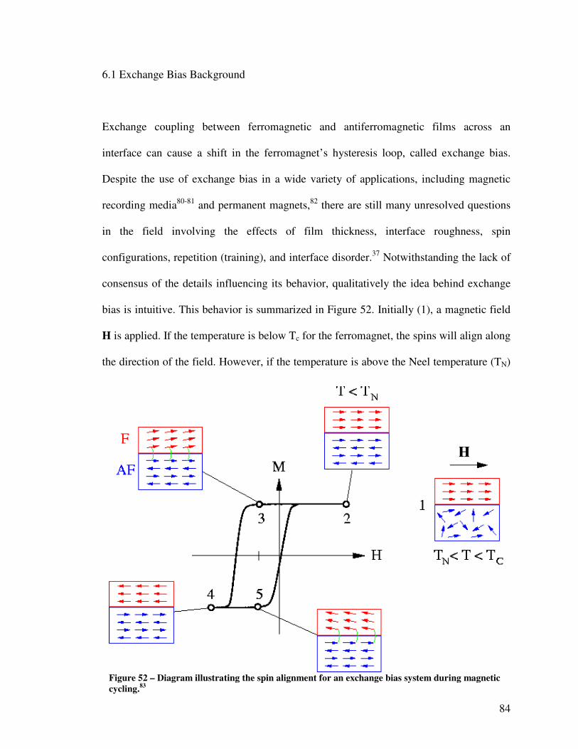
84
6.1 Exchange Bias Background
Exchange coupling between ferromagnetic and antiferromagnetic films across an
interface can cause a shift in the ferromagnet’s hysteresis loop, called exchange bias.
Despite the use of exchange bias in a wide variety of applications, including magnetic
recording media80-81
and permanent magnets,82
there are still many unresolved questions
in the field involving the effects of film thickness, interface roughness, spin
configurations, repetition (training), and interface disorder.37
Notwithstanding the lack of
consensus of the details influencing its behavior, qualitatively the idea behind exchange
bias is intuitive. This behavior is summarized in Figure 52. Initially (1), a magnetic field
H is applied. If the temperature is below Tc for the ferromagnet, the spins will align along
the direction of the field. However, if the temperature is above the Neel temperature (TN)
Figure 52 – Diagram illustrating the spin alignment for an exchange bias system during magnetic
cycling.83
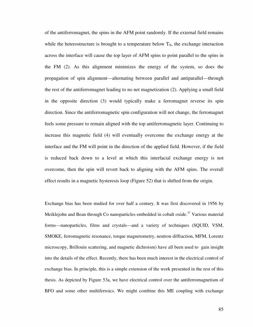
85
of the antiferromagnet, the spins in the AFM point randomly. If the external field remains
while the heterostructure is brought to a temperature below TN, the exchange interaction
across the interface will cause the top layer of AFM spins to point parallel to the spins in
the FM (2). As this alignment minimizes the energy of the system, so does the
propagation of spin alignment—alternating between parallel and antiparallel—through
the rest of the antiferromagnet leading to no net magnetization (2). Applying a small field
in the opposite direction (3) would typically make a ferromagnet reverse its spin
direction. Since the antiferromagnetic spin configuration will not change, the ferromagnet
feels some pressure to remain aligned with the top antiferromagnetic layer. Continuing to
increase this magnetic field (4) will eventually overcome the exchange energy at the
interface and the FM will point in the direction of the applied field. However, if the field
is reduced back down to a level at which this interfacial exchange energy is not
overcome, then the spin will revert back to aligning with the AFM spins. The overall
effect results in a magnetic hysteresis loop (Figure 52) that is shifted from the origin.
Exchange bias has been studied for over half a century. It was first discovered in 1956 by
Meiklejohn and Bean through Co nanoparticles embedded in cobalt oxide.37 Various material
forms—nanoparticles, films and crystals—and a variety of techniques (SQUID, VSM,
SMOKE, ferromagnetic resonance, torque magnetometry, neutron diffraction, MFM, Lorentz
microscopy, Brillouin scattering, and magnetic dichroism) have all been used to gain insight
into the details of the effect. Recently, there has been much interest in the electrical control of
exchange bias. In principle, this is a simple extension of the work presented in the rest of this
thesis. As depicted by Figure 53a, we have electrical control over the antiferromagnetism of
BFO and some other multiferroics. We might combine this ME coupling with exchange

86
coupling between an AFM and a FM (Figure 53b), resulting in electric control of
ferromagnetism (Figure 53c-d). Since the magnetoelectric coupling of BFO occurs at room
temperature, combination with a room temperature ferromagnet may result in an overall
effect that could be used in devices without the need for cooling.
6.2 Interface Control
This combination of couplings is an ambitious plan; research has demonstrated that these
two techniques—magnetoelectric and exchange coupling—work individually, but there is
no guarantee that they can work cooperatively. The first step is to grow a high quality
interface between a magnetoelectric with a ferromagnet of the appropriate critical
temperatures (above room temperature). BFO is a clear choice since it is the only room
temperature ferroelectric antiferromagnet. There are many possible choices for the
ferromagnet. CoFe is one due to its favorable anisotropy and the multitude of studies that
exist focusing on it. Figure 54a shows the heterostructure architecture. As in the previous
work, BFO(001) was grown via PLD on top of a STO substrate with a SRO bottom
FE-AFM
FM
a)
b)
c) d)
Figure 53 – Electric field control of exchange bias. Electric control of ferromagnetism (a) is
combined with exchange bias between an antiferromagnet and a ferromagnet (b) to accomplish
electric control of ferromagnetism (c). The different mechanisms and their relations can be
visualized by (d).

87
electrode to force the ferroelectric variants of BFO to point along the downward pointing
[11-1] directions. The CoFe and Ta films were then deposited via an ex-situ ion beam
sputtering process in an ultra-high vacuum deposition system at Stanford University. The
Ta layer serves as a capping layer to reduce any oxygen entering the ferromagnet from
the surface of the heterostructure. Oxide could also come from the BFO layers, reducing
the effectiveness of the coupling at the interface. As shown in Figure 54b-d, transmission
electron microscopy (TEM) and electron energy loss spectroscopy (EELS) were
performed to determine the quality of the interface. The low resolution TEM image
(Figure 54b) revealed smooth interfaces throughout the heterostructure. The high
resolution image (Figure 54c) allowed atomic resolution of the interface, and showed no
evidence of interdiffusion between the CoFe and BFO layers. This lack of interdiffusion
is considered to be important in achieving strong exchange interactions between layers.
Co0.9Fe0.1
Ta
BiFeO3
STEM
SrTiO 3
SrRuO 3
BiFeO 3Co 0.9Fe 0.1Ta
SrTiO 3
SrRuO 3
BiFeO 3Co 0.9Fe 0.1Ta
12
34
a) b)
c) d)
Figure 54 – Magnetoelectric exchange bias heterostructures and their interface. a) The materials
and spin structure of the studied heterostructure. Low (b) and high (c) resolution TEM images of
the samples. d) EELS measurement of the L-edge of cobalt.

88
EELS was used at various points throughout both the CoFe layer (Figure 54d) to confirm
that there had been no oxidation of the CoFe film. Unlike traditional exchange bias
systems, this heterostructure was not field cooled since this process resulted in significant
interdiffusion. However, the application of a magnetic field during growth appears to
have resulted in similar exchange behavior.84
6.3 Domain coupling between magnetoelectric BFO and ferromagnet CoFe
As completed in previously discussed BFO samples, the quality and ferroelectric domain
structure of the BFO layer was established prior to metal growth [Qi] using a
combination of atomic force microscopy and PFM and structural measurements. Figure
55a-b shows the out-of-plane (a) and in-plane (b) PFM images of a representative sample
location of an as-grown BFO film. The white OOP image confirms that nearly all
ferroelectric directions are pointing downward and the in-plane image reveals a
Photoemission Electron
Microscopy (PEEM)
Ou
t-o
f-p
lan
e P
iezo
forc
e
Mic
rosc
op
y (
PF
M)
In-p
lan
e P
iezo
forc
e
Mic
rosc
op
y (
PF
M)
a) c)
b) d)
e)
f)
g)
2µµµµm
Figure 13 – PFM and PEEM images demonstrating coupling between BFO and CoFe. Out-of-
plane and in-plane PFM images of a BFO thin film before poling (a-b), after poling (c-d), and
after an additional poling (e-f) compared with a PEEM image taken at the Co L-edge (g).

89
distribution of several in-plane ferroelectric directions. Figure 55c-d result from poling
the red box out-of-plane, resulting in a solid brown OOP image within the poled area.
Finally, a small area within the poled area was poled a second time in the opposite
direction (Figure 55e-f). We know from our previous data that the antiferromagnetism of
BFO follows these ferroelectric domains. By carefully marking the poled location, the
same spot was found after growth of the metallic layers.84
We observe in many samples that the CoFe magnetic domains (Figure 55g) taken by
PEEM at the Co L-edge match quite nicely with the BFO ferroelectric domains,
suggesting a coupling between the BFO domains and Co ferromagnetic domains. By
rotating the sample 45 degrees in both directions and observing the change in PEEM
contrast in images, the direction of the ferromagnetic domains can be determined. This
rotation and determination of ferromagnetic directions is shown for a small section of
Figure 55 in Figure 56. The domains with ferromagnetic directions along the direction of
a) b) c)
Figure 56 – PEEM determination of ferromagnetic directions. Co L-edge PEEM images of the
CoFe layer at sample rotation angles of (a) α=-45°°°°, (b) α=-0°°°°, and (c) α=45°°°°.

90
the incoming x-rays (red arrows in
Figure 56) have the largest intensity and
therefore appear bright. Using this fact
and the PFM images, we find that the
ferromagnetic directions are aligned
parallel with the AFM order parameter
as illustrated in Figure 57. The choice of
direction within the antiferromagnetic
axis depends on the energetically
preferable direction considering the
domain walls and any field applied
during growth of the ferromagnet.84
6.4 Horizontal Poling of BFO Domains
The next important question is whether these ferromagnetic domains can be changed if
we were to apply the electric field after growth of the metallic layers. This question
required a different approach since we cannot apply a vertical electric field through a top
conducting layer. Due to this limitation, a horizontal poling process was developed. This
new poling process made it necessary to first demonstrate a consistent poling process for
BFO before adding metallic layers on top of it. Figure 58a-b illustrates the design idea
behind our horizontal poling.
Figure 57 –Schematic diagrams of two adjacent
domains (a,c) in the BFO(001) film, in which the
[111] polarization directions as well as the
perpendicular antiferromagnetic plane are
identified as well as their projections onto the [001] surface and the corresponding M-directions in the CoFe layer (b,d).

91
The bottom electrode SRO is grown in a manner consistent with previous samples;
however, photolithography and ion milling is used to etch away most of the SRO,
allowing the remainder to become our poling electrodes. 100-150 nm of BFO is then
grown like a blanket on top of the SRO electrodes and space between. The metallic layers
grown by ultra-high vacuum metal deposition as before are also taken through another
round of photolithography and ion milling leaving behind only small stripes of CoFe on
top of BFO and in between the SRO electrodes. This design allows us to change the BFO
electrically and see what happens to the ferromagnetic on top.
The BFO domains in this architecture behave similarly to the BFO(001) domains
previously discussed. Figure 58c illustrates that we get very nice controllable stripes that
a)
b)
c)
d)
e)
Figure 58 - Horizontal switching device structure. Three-dimensional (a) and cross-sectional (b)
schematic diagrams of the coplanar epitaxial electrode device illustrating the structure that will
enable controlled ferroelectric switching and electrical control of local ferromagnetism in the
CoFe features. In-plane PFM images showing the ferroelectric domain structure for a device in
the as-grown state (c), after the first electrical switch (d) and after the second electrical switch (e).
92
make a 45 degree angle to the electrodes. This angle is actually due to the choice of
aligning the electrodes along this direction. Rotation of the electrodes by 45 degrees
resulted in unreliable control of both BFO and CoFe domains. The domains rotate by 90
degrees when poled with an electric field (Figure 58d). This process is also reversible
when the electric field is applied along the opposite direction (Figure 58e). Thus,
horizontal poling of BFO ferroelectric domains is controllable and reversible.84
6.5 Electric Field Control of CoFe Ferromagnetism
Now that we are confident about our BFO processing, let us consider how the
ferromagnetic domains change through this poling. The ovals in Figure 59a-c are the Co
As grown First E switch Second E switch
a) b) c)
d) e) f)
Figure 59 - Electrical control of local ferromagnetism. XMCD–PEEM images taken at the Co L-
edge revealing the ferromagnetic domain structure of the CoFe features in the coplanar electrode
device structure in the as-grown state (a), after the first electrical switch (b) and after the second
electrical switch (c). Schematic descriptions of the observed magnetic contrast (grey, black and
white) in the corresponding XMCD–PEEM images, respectively. Application of an electric field is
found to rotate the next magnetization of the structures by 90°°°° . The direction of the applied
growth field and the incoming X-ray direction are labeled.

93
stripes on top of BFO with the electrodes on the sides of the images. The variation of
colors in the stripes represents the different ferromagnetic directions. In Figure 59a and
59d, the two as-grown ferromagnetic directions lie on either side of the applied magnetic
field during growth of the ferromagnet, resulting in a net magnetization along the
direction of applied field. When we apply an electric field across the electrodes, there is a
clear change in the ferromagnetic domains. As demonstrated by the near reversal of
contrast, the ferromagnetic directions and therefore net magnetization rotates by 90
degrees and rotates back after another poling in the opposite direction. Though
admittedly not perfect, this is a demonstration of electrical control of ferromagnetism at
room temperature.84
This is clearly a very exciting result, but there is still much more to determine. Why do
the ferromagnetic domains not match the ferroelectric domains as in the vertical poling?
What are the competing energies? For example, notice that the ferromagnetic domains do
not always change on the ends of the metallic stripes. Why is there an apparent 180
degree reversal of some ferromagnetic domains and no change in others? Why would
electrical control of an antiferromagnetic axis (which should have no preference between
left or right) result in a change in the ferromagnetic direction? It seems likely that the
picture is not as simple as magnetoelectric and then exchange coupling. It may very well
be that strain mediates this effect, causing an imbalance between left and right directions.
Many questions are left unanswered. Though clearly there is much room here for future
work, it is important to point out that many questions also still remain in standard
exchange bias even though the effect is a multi-billion dollar money maker in a wide

94
variety of applications. Perhaps this electrical control of ferromagnetism at room
temperature can also be put to use well before intricacies are established, or this extra
electric order parameter may allow a new perturbation of exchange bias that could unlock
its mysteries.
95
Chapter 7: Summary of Results and Future Directions
7.1 Introduction
This thesis has focused on electric and strain control of antiferromagnetism, as well as
ferromagnetism at room temperature through the use of multiferroic, magnetoelectric
BFO films. Chapter 1 discussed what properties define a multiferroic and magnetoelectric
material and touched on applications using these individual properties. BFO was
introduced as a model system, being the only room temperature ferroelectric
antiferromagnet. Finally, this chapter ended with a brief summary of the organization of
this dissertation.
Though this work shows great promise for the use of BFO in practical applications, other
magnetoelectrics should be considered. BFO has a clear advantage in being the only
single phase room temperature ferroelectric antiferromagnet. However, the combination
of two or more materials, such as a ferroelectric (like PZT) and a ferromagnet could
result in a strong interfacial magnetoelectric effect and is a hot research area. In fact, it is
possible that this could be achieved without the need of ferroelectric and magnetic layers.
The appropriate use of strain and layering has resulted in thin film ferroelectrics (when
the bulk material was not ferroelectric) and interfacial magnetism between non-magnetic
materials. There is no reason to assume that such ideas could not also be used to create
interfacial magnetoelectricity. Second harmonic generation, sensitive to both electric and
magnetic fields at interfaces, would be a perfect tool to search for such behavior.

96
7.2 Techniques for Measurement
Chapter 2 gave the background required to understand the x-ray techniques used to study
BFO in the rest of the thesis. Photoemission electron microscopy is a powerful technique
that takes advantage of the sensitivity of x-ray absorption spectroscopy to excited states
in materials. The dichroism effect observed in magnetic and ferroelectric materials is
utilized in PEEM to image the domains. We use these domain images to study the control
of magnetism in BFO in this research.
7.3 Electric Control of Antiferromagnetism in BFO
Chapter 3 began the discussion of the first experimental results in this work. A
conceptual approach to electrically control of antiferromagnetism in BFO thin films was
presented. PFM and PEEM images were compared to determine the effectiveness of this
approach. The sensitivity of PEEM to ferroelectric domains and how one can separate
this effect from the magnetic effect through temperature dependent measurements was
addressed. Finally, this work was confirmed by electrical control of magnetism in BFO
crystals by Lebeugle et. al. Though electric control has been proven for bulk and films
greater than 100 nm, no conclusive result exists yet for thinner BFO films. This is largely
due to the fact that the BFO domains get smaller with decreasing BFO thickness,
eventually approaching the resolution limit of PEEM. As the resolution of PEEM
improves, it would be interesting to study this coupling for ultrathin films where the
ferroelectric and magnetic properties differ, as discussed in the next chapter.
97
7.4 Thickness Effect on Properties of BFO
Chapter 4 was a lengthy chapter representing the bulk of the effort in this research. Thin
BFO films were observed to deviate from the behavior observed in bulk. Strain (via
control of film thickness) was introduced as a method to further control (beyond the
electric control presented in the last chapter) the magnetic properties of BFO. Though the
measurements in the previous chapter were sufficient to demonstrate electric control of
antiferromagnetism, the exact antiferromagnetic nature could not distinctly be
determined. Much effort was taken to model the angular dependencies of many possible
magnetic behaviors for BFO and determine the best experiment to distinguish between
these possibilities. The ferroelectric contribution also had to be approximated to allow the
correct angular dependencies. This ferroelectric research represents a large area for future
research. PEEM imaging of ferroelectrics has not been largely investigated. Though the
ferroelectric angular dependence appears to be similar to magnetic contributions,
questions remain. For example, it is observed that polarization domains pointing out of
the sample versus into it result in dramatically different PEEM contrast, despite being a
difference of 180 degrees. In magnetic contrast, a change of 180 degrees cannot be
determined through linear dichroism measurements.
An approximate formula for the angular dependence of PEEM contrast in a multiferroic
was created and used to distinguish a preferred [112]-type magnetic axis in BFO thin
films, as opposed to the easy magnetic plane seen in bulk. It is important to note that the
98
concepts behind this formula can be used not only for other multiferroics but also for
other materials with more than one angle- or temperature-dependent contribution to linear
dichroism. This formulation is particularly important when it has recently been
discovered85
that crystallographic directions play a significant role in x-ray absorption
measurements. It should be noted, however, that though dichroism images are derived
from x-ray absorption spectroscopy, the division of images and comparison of domains
with the same crystallographic contributions in PEEM can result in a cancellation of
some components.
Finally, Chapter 4 investigated the change of ferroelectric and magnetic properties in
ultathin films with film thickness less than 20 nm. The ferroelectric and magnetic
properties weaken as the film thickness becomes quite small, an effect found by both
PFM and XAS. This observation is in agreement and correlates well with the reduction of
exchange bias seen in ferromagnets on very thin antiferromagnets.
7.5 Orientation Effects on the Ferroelectric and Magnetic Properties of BFO
Chapter 5 studied the differences in ferroelectric and magnetic properties between
different orientations of BFO thin films. 110 and 111 orientations were introduced as
alternatives to the 001 structure discussed throughout the rest of the thesis. Thick
BFO(110) films show easy plane behavior as opposed to <112> axes selected in thin
films. BFO(111) films reveal no dichroism but variation in PEEM images, meaning easy

99
plane behavior for all thicknesses. No preferred axis is selected in this orientation since
the strain is applied symmetrically across the perpendicular magnetic plane.
7.6 Exchange Bias with BFO
Chapter 6 utilized the knowledge from the previous chapters to establish electric control
of ferromagnetism. This was accomplished through a combination of magnetoelectric
coupling and exchange bias. The growth of high-quality films allowed strong coupling
between BFO domains and the ferromagnetic domains of CoFe. A horiztonal poling
device was created in order to observe the effect on a top layer of CoFe when BFO was
electrically pole underneath. A near-reversal of ferromagnetic domains was observed,
providing strong evidence for the possibility of electrical control of ferromagnetism at
room temperature—the goal of this thesis.
There are many ways this electrically assisted exchange bias research could be enhanced.
For example, other ferromagnetic materials should be studied to find the most efficient
control. Pure Co was attempted with little success. However, some believe better
coupling could be achieved with an oxide such as LSMO. Both BFO and LSMO have
perovskite structures and could be grown in-situ to get epitaxial structure, and therefore
have the advantage of maintaining the chemical structure across the interface. One could
expect that such heterostructure has stronger exchange interaction than the amorphous
BFO/CoFe structure. Moreover, since the dramatic physics properties of both BFO
(multiferroic) and LSMO (well-known colossal magnetoresistance oxide) are well

100
studied, the interaction between these two materials will involve spin and orbital orders
and will likely result in fascinating physics.
The mechanisms and magnitudes of competing energies most relevant in electric
exchange bias are not known. For instance, shape anisotropy was considered by varying
the length to width ratio of the CoFe stripes. The only clear result of this study was that
domain wall pinning was more common on the short edges of each stripe. Why? What
other energies are most important? Is the electric control just the result of magnetoelectric
coupling and exchange bias, or is there a mediating effect such as strain?
7.7 Overall Summary
Electric and strain control of antiferromagnetism and ferromagnetism at room
temperature using magnetoelectric BFO thin films has been demonstrated and modeled.
PFM and PEEM techniques were used to correlate ferroelectric and antiferromagnetic
domains. A formula was established and applied to determine magnetic behavior. The
effect of thickness and orientation on ferroelectric and magnetic properties was studied.
Finally, this knowledge was used in the making of a magnetoelectric-ferromagnetic
heterostructure in which electrically-assisted exchange bias was observed. This toolbox
of control parameters gives us a very strong benefit for the making of new and improved
devices, particularly in the computing industry where the traditional magnetic field
controlled devices are reaching their limits.

101
Appendix A: Growth of Epitaxial BFO Thin Films
Epitaxial growth is the extended single-crystal film formation on top of a crystalline
substrate. High quality epitaxial growth has only recently become a common practice and has
allowed significant improvement in computing and other device functionality. Although there
are many methods that allow high quality film growth, nearly all films in this research were
obtained by pulsed laser deposition. In PLD, a laser shines onto a target powder that that has
all of the atoms desired for the final film. The laser creates a highly directional plume of
atoms that deposit on a substrate that can be heated in a gaseous environment. The
combination of temperature and gas pressure control allows for a wide range of
thermodynamic conditions. The majority of the BFO films in this study were grown using
PLD at 700°C in 100 mTorr partial pressure of oxygen and then cooled at 5°C/minute to
room temperature in 760 Torr pressure of oxygen. XRD measurements allowed
measurements of lattice constants and verified that the films were single phase. Before
growth of the BFO layer, a SRO layer is deposited on a high quality single crystal
heterostructure (typically STO or DSO due to their close lattice match with BFO). The
SRO layer serves to break the energy degeneracy between the different ferroelectric
directions. In BFO(001) films, this results in only four downward pointing ferroelectric
directions instead of all eight possible directions. The degeneracy between the four
directions can be further broken by growing on a miscut substate. Since a miscut
substrate is not flat, but instead slants at a small angle, the BFO ferroelectric direction
pointing along the miscut will be present in a monodomain film. A miscut in-between
two ferroelectric directions will result in a film with two ferroelectric directions, creating
a stripe domain pattern.

102
Appendix B: Piezoelectric Force Microscopy
Piezoelectric force microscopy measures both the out of plane force and the torque on the
PFM tip when the tip has an oscillating voltage applied to it.10-11
The out of plane mode
will determines whether the material one of the four up- or downward pointing body
diagonal directions. The in plane mode distinguishes between these four directions. By
comparing these two modes, one can distinguish which polarization direction is present.12
For example, Figure 60 shows the out of plane (a and c) and in-plane (b and d) PFM
images before (a and b) and after (c and
d) applying an external electric field of
12 V. The cantilever tip comes in from
the right of the images. In the in-plane
images, the colors black, white and
brown represent whether the cantilever
tip is torqued right, left or not
horizontally. This color determines the
in plane direction of the polarization.
The white color in Figure 60a,
demonstrates that only downward
pointing ferroelectric directions are
present before poling, but the application
of the external electric field results in
only upward (black) pointing
PPPP3333
++++
109°°°°
71°°°°
180°°°°
(a)
(d)
(b)
(c)
⊗⊗⊗⊗
•• PPPP1111
++++
PPPP1111
----
PPPP1111
++++
PPPP1111
----
PPPP1111
----
PPPP4444
----
(e)
PPPP1111
----
PPPP4444
----PPPP1111
----
PPPP4444
----
2µµµµm
Figure 60 - Out-of-plane (a) and in-plane (b)
PFM images of the as-grown BFO film. Out-of-
plane (c) and in-plane (d) PFM images taken
after applying an electric field perpendicular to
the film on the same area as in a and b. Different
polarization switching mechanisms are shown by
the arrows in (d). A side view of two observed
ferroelectric variants (e).

103
ferroelectric directions within the poled box. The arrows in Figure 60d indicate new in-
plane polarization directions after ferroelectric switching. Different polarization
switching mechanisms (71°, 109° and 180°) are labeled in Figure 60d. Figure 60e
illustrates the side view of two predominant polarization directions in this film.

104
REFERENCES
1. H.-U. Habermeier, Materials Today 10 (10), 34 (2007).
2. E. Dagotta, Science 309, 257 (2005).
3. Y. Tokura and N. Nagosa, Science 288, 462 (2000).
4. W. Känzig, "Ferroelectrics and Antiferroelectrics". in Frederick Seitz, T. P. Das,
David Turnbull, E.L. Hahn, Solid State Physics. 4. Academic Press. p. 5. (1957).
5. M. Lines and A. Glass, Principles and applications of ferroelectrics and related
materials. Clarendon Press, Oxford (1979).
6. K. Aizu, Phys. Rev. B 2, 754 (1970).
7. J.F. Scott, Ferroelectric Memories. Springer (2000).
8. M. Dawber, K.M. Rabe, and J.F. Scott, Reviews of Modern Physics 77: 1083 (2005).
9. S.V. Kiselev, et al., Soviet Phys.-Doklady 7:742-744 (1963).
10. P. Günther, et al., Appl. Phys. Lett. 61, 1137 (1992).
11. A. Gruverman, et al., Annu. Rev. Mater. Sci. 28, 101 (1998).
12. F. Zavaliche, et al., Phase Transit. 79, 991 (2006).
13. L. Fritsche and B. Weimert, Phys. Stat. Sol. B 208, 287 (1998).
14. C. Ederer and N. Spaldin, Phys. Rev. B 95, 224103 (2005).
15. R. Ramesh, et al., Nature Mater. 6, 21 (2007).
16. S.-W. Cheong, et al., Nature Mater. 6, 13 (2007).
17. N.A. Hill, J. Phys. Chem. B 104, 6694 (2000).
18. M. Fiebig, J. Phys. D Appl Phys. 38 R1123 (2005).
19. W. Eerenstein, et al., Nature 442, 759 (2006).
20. V.E. Wood and A.E. Austin, et al., Int. J. Magn. 5, 303 (1973).

105
21. G.C. Baldwin, Physics Today 28 (1), 9 (1975).
22. J. Stohr and S. Anders, IBM J. Res. Develop. 44 (4), 535 (2000).
23. E. Brüche, Z. Phys. 86, 448 (1933).
24. G. Schonhense, J.Phys.: Condens. Matter 11, 9517-9547 (1999).
25. E. Bauer, J. Phys. Cond. Mat. 13, 11391 (2001).
26. B.P. Tonner and G.R. Harp, Rev. Sci. Instrum. 59, 853 (1988).
27. W. Engel, et al., Ultramicroscopy 36, 148 (1991).
28. S. Anders et al., Rev. of Sci Inst, 70, 10 (1999).
29. G. van der Laan and B. T. Thole, Phys. Rev. B 43, 13401 (1991).
30. B.T. Thole, et al., Phys .Rev. Lett. 68 1943 (1992).
31. J. Stohr, J. Magn. Magn. Mater. 200, 470 (1999).
32. H. Ohldag, et al., J. Elec. Spect. Rel Phen., 114, 765 (2001).
33. F.U. Hillebrecht, et al., Phys Rev. Lett., 86, 152878 (2001).
34. A. Scholl, et al, Science 287, 1014 (2000).
35. D. Spanke, et al., Phys. Rev. B 58, 5201 (1998).
36. J. Stohr, Phys. Rev. Lett., 83, 1862 (1999).
37. J. Nogues, J. Magn. Magn. Mater. 192, 203 (1999).
38. M. Kiwi, J. Magn. Magn. Mater. 234, 584 (2001).
39. J.C.S. Kools, IEEE Trans. Magn. 32, 3165 (1996).
40. N. Smith, “Science with Soft X-rays,” Physics Today, January (2001).
41. H. Ohldag, Phys. Rev. Lett. 87 247201 (2001).
42. H. Ohldag, Appl. Phys.Lett. 76, 2928 (2000).
43. K. Takano, et al., Phys. Rev. Lett. 78, 1130 (1997).
106
44. N.C. Koon, Phys. Rev. Lett. 78, 4865 (1997).
45. T.C. Schulthess, Phys. Rev. Lett. 81, 4516 (1998).
46. P. Miltenyi, et al., , Phys. Rev. Lett. 84, 4224 (2000).
47. T. Zhao, et al., Nature Mat. 5, 825 (2005).
48. W.-C. Yang, et. al., Appl Phys. Lett. 85 (12), 2316 (2004).
49. C. Ederer and N. Spaldin, Phys. Rev. Lett. 95, 257601 (2005).
50. R.R. Das, et al., Appl. Phys. Lett. 88, 242904 (2006).
51. M. Fiebig, et al., Nature 419, 818 (2002).
52. J. Dho, et al., Adv. Mater. 18, 1445–1448 (2006).
53. D. Lebeugle, et. al., Phys. Rev. Lett. 100, 227602 (2007).
54. S. V. Kiselev, R. P. Ozerov, and G. S. Zhdanov, Sov. Phys. Dokl. 7, 742 (1963).
55. J. R. Teague, R. Gerson, and W. J. James, Solid State Commun. 8, 1073 (1970).
56. I. Sosnowska, et al., J. Phys. C 15, 4835 (1982).
57. S. Lee, et al., Phys. Rev. B 78, 100101(R) (2008).
58. B. Ruette, et. al., Phys. Rev. B 69, 064114 (2004).
59. C. Tabares-Munoz, et al., Ferroelectrics 55, 235-238 (1984).
60. Y.F. Popov, et. al., Low Temperature Physics 27 (4), 478 (2001).
61. J. Wang et. al., Science 299 1719 (2003).
62. Q. Jiang and J.H. Qui, J. of Appl. Phys. 99, 103901 (2006).
63. D.G. Schlom, et. al., Annu. Rev. Mater. Res. 37, 589 (2007).
64. Y.H. Chu, et al., Appl. Phys. Lett. 90, 252906 (2007).
65. C. Ternon, et al., Thin Solid Films 515 (2), 481 (2006).
66. A.J. Millis, et al., J. of Appl. Phys. 83 (3):1588-1591 (1998).

107
67. T. Yamada, J. Phys. Soc. Jpn. 21, 664 (1966).
68. A.K. Zvezdin, et al., Jour. of Magnetism and Magnetic Mat. 300 (1), 224 (2006).
69. M.B. Holcomb, et al.,Phys. Rev. B, in revision (2009).
70. J. Stohr and H.C. Siegmann, Magnetism From Fundamentals to Nanoscale Dynamics
(Springer: New York, 2006).
71. T. Tsuboi, Phys. Rev. B 39, 2842 (1989).
72. A. Gruverman, et al., Annu. Rev. Mater. Sci. 28, 101 (1998).
73. A. Scholl, et al., Rev. Of Sci. Instr. 73 (3), 1362 (2002).
74. T. Ambrose and C.L. Chien, Phys. Rev. Lett. 76(10), 1743 (1996).
75. J.W. Seo, et al., (2008) J. Phys. Cond. Mat. 20, 264014 (2008).
76. N. Setter, et al., J. of Appl. Phys. 100, 051606 (2006).
77. M. Huijben, et al., Phys. Rev. B 78, 094413 (2008).
78. G. Xu, J. Li, and D. Viehland, Appl. Phys. Lett. 89, 222901 (2006).
79. J. Lüning, et al.,, Phys. Rev. B 67, 214433 (2003).
80. M. Ohkoshi, et al., IEEE Transl. J. Magn. Jpn. 1, 37 (1985).
81. A. A. Glazer, et al., Sov. Phys. JETP Lett. 15, 259 (1972).
82. F. S. Lubrosky, Electro-Technology, 102 (Sept. 1962).
83. M. Kirschner, http://magnet.atp.tuwien.ac.at/gallery/exchbias/intuitive.html
84. Y. H. Chu, et al., Nat. Mat., 7 (6) 478 (2008).
85. E. Arenholz, et al., Phys. Rev. B 74, 094407 (2006).