a high performance multibit with sacd ... - analog devices · information furnished by analog...
TRANSCRIPT

REV. 0
a
Information furnished by Analog Devices is believed to be accurate andreliable. However, no responsibility is assumed by Analog Devices for itsuse, nor for any infringements of patents or other rights of third parties thatmay result from its use. No license is granted by implication or otherwiseunder any patent or patent rights of Analog Devices.
One Technology Way, P.O. Box 9106, Norwood, MA 02062-9106, U.S.A.
Tel: 781/329-4700 www.analog.com
Fax: 781/326-8703 © Analog Devices, Inc., 2002
AD1955
High Performance Multibit - DACwith SACD Playback
FEATURES
5 V Power Supply Stereo Audio DAC System
Accepts 16-/18-/20-/24-Bit Data
Supports 24-Bit, 192 kHz Sample Rate PCM Audio Data
Supports SACD Bit Stream and External Digital Filter
Interface
Accepts a Wide Range of PCM Sample Rates Including:
32 kHz, 44.1 kHz, 48 kHz, 88.2 kHz, 96 kHz, and
192 kHz
Multibit Sigma-Delta Modulator with "Perfect Differen-
tial Linearity Restoration" for Reduced Idle Tones and
Noise Floor
Data Directed Scrambling DAC––Low Sensitivity to Jitter
Supports SACD Playback with "Bit Expansion" Filter
Differential Current Output for Optimum Performance
8.64 mA p-p Differential Output
120 dB SNR/DNR (not muted) at 48 kHz Sample Rate
(A-Weighted Stereo)
123 dB SNR/DNR (Mono)
–110 dB THD + N
110 dB Stop-Band Attenuation with 0.0002 dB
Pass-Band Ripple
8 Oversampling Digital Filter
On-Chip Clickless Volume Control
Supports SACD-Mute Pattern Detection
Supports 64 fS/128 fS DSD SACD with Phase Mode
Internal Digital Filter Pass-Through for External Filter
Master Clock: 256 fS, 512 fS, 768 fS
Hardware and Software Controllable Clickless Mute
Serial (SPI) Control for Serial Mode, Number of Bits,
Sample Rate, Volume, Mute, De-Emphasis, Mono Mode
Digital De-Emphasis for 32 kHz, 44.1 kHz, and 48 kHz
Sample Rates
Flexible Serial Data Port with Right-Justified, Left-
Justified, I2S, and DSP Modes
28-Lead SSOP Plastic Package
APPLICATIONS
High End DVD Audio
SACD
CD
Home Theater Systems
Automotive Audio Systems
Sampling Musical Keyboards
Digital Mixing Consoles
Digital Audio Effects Processors
FUNCTIONAL BLOCK DIAGRAM
AUTO-CLOCKDIVIDER SPI CONTROL
MASTERCLOCK INPUT
CONTROLDATA INPUT
3
DIGITALSUPPLY
DSDBITSTREAM
INPUT
MUX
SERIAL DATAINTERFACE
EXTERNALFILTER I/F
DIGITALFILTER ENGINE
S/H
MULTIBIT -MODULATOR
NOISE-SHAPEDSCRAMBLING
16-/20-/24-BITAUDIO DATA/
EXTERNALDIGITAL
FILTER INPUT
3/4DSD FILTER
RESET
MUTE
ANALOGSUPPLY
ZEROFLAGS
I-DAC
L-CH R-CHDIFFERENTIAL
CURRENT OUTPUT
I-DACVOLTAGE
REFERENCE
4
PRODUCT OVERVIEWThe AD1955 is a complete, high performance, single-chip, stereodigital audio playback system. It is comprised of a multibit sigma-delta modulator, high performance digital interpolation filters,and continuous-time differential current output DACs. Otherfeatures include an on-chip clickless stereo attenuator and mutecapability, programmed through an SPI compatible serial controlport. The AD1955 is fully compatible with all known DVD audioformats including 192 kHz as well as 96 kHz sample frequenciesand 24 bits. It is also backward compatible by supporting 50 µs/15 µs digital de-emphasis intended for “redbook” compact discs,as well as de-emphasis at 32 kHz and 48 kHz sample rates.
The AD1955 has a very flexible serial data input port thatallows for glueless interconnection to a variety of ADCs, DSPs,SACD decoders, external digital filters, AES/EBU receivers, and
(continued on page 12)

REV. 0–2–
AD1955–SPECIFICATIONS
ANALOG PERFORMANCEParameter Min Typ Max Unit
Resolution 24 Bits
SIGNAL-TO-NOISE RATIO (20 Hz to 20 kHz)*Differential Output (A-Weighted, RMS) (Stereo) 120 114 dBDifferential Output (A-Weighted, RMS) (Mono) 123 dBSingle-Ended (A-Weighted, RMS) (Stereo) 119 dB
DYNAMIC RANGE (20 Hz to 20 kHz, –60 dB Input)*Differential Output (A-Weighted, RMS) (Stereo) 120 114 dBDifferential Output (A-Weighted, RMS) (Mono) 123 dBSingle-Ended (A-Weighted, RMS) (Stereo) 119 dB
Total Harmonic Distortion + Noise (Stereo) at 0 dBFS –110 –102.5 dB
ANALOG OUTPUTSDifferential Output Range (Full Scale) 8.64 mA p-pOutput Capacitance at Each Output Pin 100 pFOutput Bias Current, Each Output –3.24 mA
Out-of-Band Energy (0.5 fS to 100 kHz) –90 dBReference Voltage 2.245 2.39 2.505 V
DC ACCURACYGain Error ±6 %Interchannel Gain Mismatch 0.01 0.26 dBGain Drift 25 ppm/°C
Interchannel Crosstalk (EIAJ Method) –125 dBInterchannel Phase Deviation ±0.1 DegreesMute Attenuation –100 dBDe-Emphasis Gain Error ±0.1 dB
*Measured with Audio Precision System Two Cascade in RMS Mode. Averaging Mode will show approximately 2 dB better performance.
Performance of right and left channels are identical (exclusive of the Interchannel Gain Mismatch and Interchannel Phase Deviation specifications).
Specifications subject to change without notice.
TEST CONDITIONS(Unless otherwise noted.)Analog Supply Voltages (AVDD) . . . . . . . . . . . . . . . . . . . . 5 VDigital Supply Voltages (DVDD) . . . . . . . . . . . . . . . . . . . . 5 VReference Current (IREF) . . . . . . . . . . . . . . . . . . . . . 0.960 mAAmbient Temperature . . . . . . . . . . . . . . . . . . . . . . . . . . . 25°CInput Clock . . . . . . . . . . . . . . . . . . . . . . . . . . . . . 12.288 MHzInput Signal . . . . . . . . . . . . . . . . . 984.375 Hz, 0 dB Full ScaleInput Sample Rate . . . . . . . . . . . . . . . . . . . . . . . . . . . . 48 kHzMeasurement Bandwidth . . . . . . . . . . . . . . . . 20 Hz to 20 kHzWord Width . . . . . . . . . . . . . . . . . . . . . . . . . . . . . . . . . 24 BitsLoad Capacitance . . . . . . . . . . . . . . . . . . . . . . . . . . . . 100 pFLoad Impedance . . . . . . . . . . . . . . . . . . . . . . . . . . . . . . 47 kΩInput Voltage HI . . . . . . . . . . . . . . . . . . . . . . . . . . . . . . . 2.4 VInput Voltage LO . . . . . . . . . . . . . . . . . . . . . . . . . . . . . . 0.8 V
(See figures. IREF = 0.960 mA, VBIAS = 2.80 V.)
REV. 0
AD1955
–3–
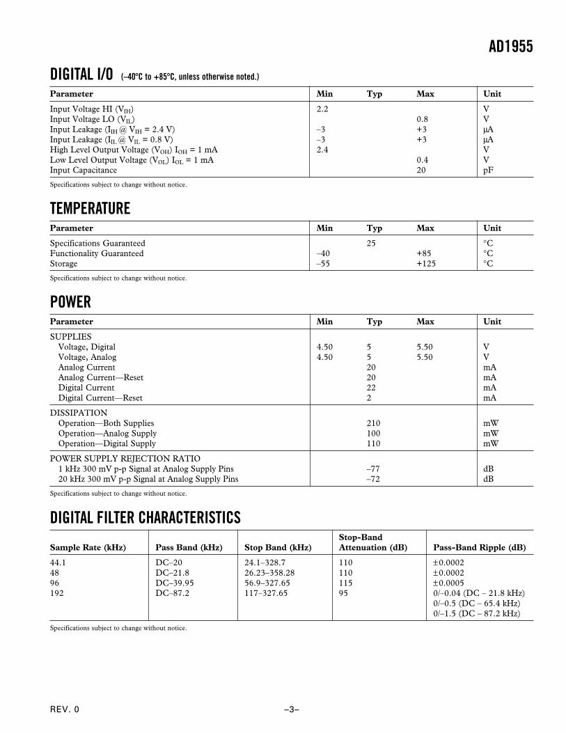
DIGITAL I/O (–40C to +85C, unless otherwise noted.)
Parameter Min Typ Max Unit
Input Voltage HI (VIH) 2.2 VInput Voltage LO (VIL) 0.8 VInput Leakage (IIH @ VIH = 2.4 V) –3 +3 µAInput Leakage (IIL @ VIL = 0.8 V) –3 +3 µAHigh Level Output Voltage (VOH) IOH = 1 mA 2.4 VLow Level Output Voltage (VOL) IOL = 1 mA 0.4 VInput Capacitance 20 pF
Specifications subject to change without notice.
TEMPERATUREParameter Min Typ Max Unit
Specifications Guaranteed 25 °CFunctionality Guaranteed –40 +85 °CStorage –55 +125 °CSpecifications subject to change without notice.
POWERParameter Min Typ Max Unit
SUPPLIESVoltage, Digital 4.50 5 5.50 VVoltage, Analog 4.50 5 5.50 VAnalog Current 20 mAAnalog Current—Reset 20 mADigital Current 22 mADigital Current—Reset 2 mA
DISSIPATIONOperation—Both Supplies 210 mWOperation—Analog Supply 100 mWOperation—Digital Supply 110 mW
POWER SUPPLY REJECTION RATIO1 kHz 300 mV p-p Signal at Analog Supply Pins –77 dB20 kHz 300 mV p-p Signal at Analog Supply Pins –72 dB
Specifications subject to change without notice.
DIGITAL FILTER CHARACTERISTICSStop-Band
Sample Rate (kHz) Pass Band (kHz) Stop Band (kHz) Attenuation (dB) Pass-Band Ripple (dB)
44.1 DC–20 24.1–328.7 110 ±0.000248 DC–21.8 26.23–358.28 110 ±0.000296 DC–39.95 56.9–327.65 115 ±0.0005192 DC–87.2 117–327.65 95 0/–0.04 (DC – 21.8 kHz)
0/–0.5 (DC – 65.4 kHz)0/–1.5 (DC – 87.2 kHz)
Specifications subject to change without notice.

REV. 0–4–
AD1955
SPECIFICATIONS (continued)
GROUP DELAYChip Mode Group Delay Calculation fS (kHz) Group Delay Unit
INT8 Mode 5553/(128 fS) 48 903.8 µsINT4 Mode 5601/(64 fS) 96 911.6 µsINT2 Mode 5659/(32 fS) 192 921 µs
Specifications subject to change without notice.
DIGITAL TIMING (Guaranteed over –40C to +85C, AVDD = DVDD = 5.0 V 10%.)
Parameter Description Min Unit
tDMP MCLK Period (FMCLK = 256 FLRCLK) 50 nstDML MCLK LO Pulsewidth (All Modes) 0.4 tDMP nstDMH MCLK HI Pulsewidth (All Modes) 0.4 tDMP nstDBH BCLK/EF_BCLK High 20 nstDBL BCLK/EF_BCLK Low 20 nstDBP BCLK/EF_BCLK Period 60 nstDLS LRCLK/EF_WCLK Setup 0 nstDLH LRCLK Hold (DSP Serial Port Mode Only) 15 nstDWH EF_WCLK High 20 nstDWL EF_WCLK Low 20 nstDDS SDATA/EF_LDATA/EF_RDATA Setup 0 nstDDH SDATA/EF_LDATA/EF_RDATA Hold 20 nstDPHS DSD_PHASE Setup 20 nstDSDS DSD_DATA Setup 5 nstDSDH DSD_DATA Hold 5 nstDSKP DSD_SCLK Period 60 nstDSKH DSD_SCLK High 20 nstDSKL DSD_SCLK Low 20 nstDMP CCLK Period 50 nstDML CCLK LO Pulsewidth 15 nstDMH CCLK HI Pulsewidth 10 nstCLS CLATCH Setup 0 nstCLH CLATCH Hold 15 nstCDS CDATA Setup 0 nstCDH CDATA Hold 5 nstRSTL RST LO Pulsewidth 10 ns
Specifications subject to change without notice.

REV. 0
AD1955
–5–
CAUTIONESD (electrostatic discharge) sensitive device. Electrostatic charges as high as 4000 V readilyaccumulate on the human body and test equipment and can discharge without detection. Although theAD1955 features proprietary ESD protection circuitry, permanent damage may occur on devicessubjected to high energy electrostatic discharges. Therefore, proper ESD precautions are recommendedto avoid performance degradation or loss of functionality.
WARNING!
ESD SENSITIVE DEVICE
PIN CONFIGURATION
ABSOLUTE MAXIMUM RATINGS*
Parameter Min Max Unit
DVDD to DGND –0.3 6 VAVDD to AGND –0.3 6 VDigital Inputs DGND – 0.3 DVDD + 0.3 VAnalog Outputs AGND – 0.3 AVDD + 0.3 VAGND to DGND –0.3 +0.3 VReference Voltage (AVDD + 0.3)/2Soldering 300 °C
10 sec
*Stresses greater than those listed under Absolute Maximum Ratings may causepermanent damage to the device. This is a stress rating only; functional operationof the device at these or any other conditions above those indicated in theoperational section of this specification is not implied. Exposure to absolutemaximum rating conditions for extended periods may affect device reliability.
PACKAGE CHARACTERISTICS
Package Typ Unit
JA (Thermal Resistance 109.0 °C/W[Junction-to-Ambient])
JC (Thermal Resistance 39.0 °C/W[Junction-to-Case])
ORDERING GUIDE
Model Temperature Package Description Package Option*
AD1955ARS –40°C to +85°C 28-Lead SSOP RS-28AD1955ARSRL –40°C to +85°C 28-Lead SSOP RS-28 on 13" ReelsEVAL-AD1955EB Evaluation Board
*RS = Shrink Small Outline Package
TOP VIEW(Not to Scale)
28
27
26
25
24
23
22
21
20
19
18
17
16
15
1
2
3
4
5
6
7
8
9
10
11
12
13
14IREF
FILTR
IOUTR–
IOUTR+
AGND
DSD_PHASE
DSD_RDATA
DVDD
LRCLK/EF_WCLK
BCLK/EF_BCLK
SDATA/EF_LDATA
DSD_LDATA
DSD_SCLK
EF_RDATA
AVDD
FILTB
IOUTL–
IOUTL+
AGND
ZEROR
ZEROL
DGND
MCLK
CCLK
CLATCH
MUTE
PD/RST
CDATA
AD1955
REV. 0–6–
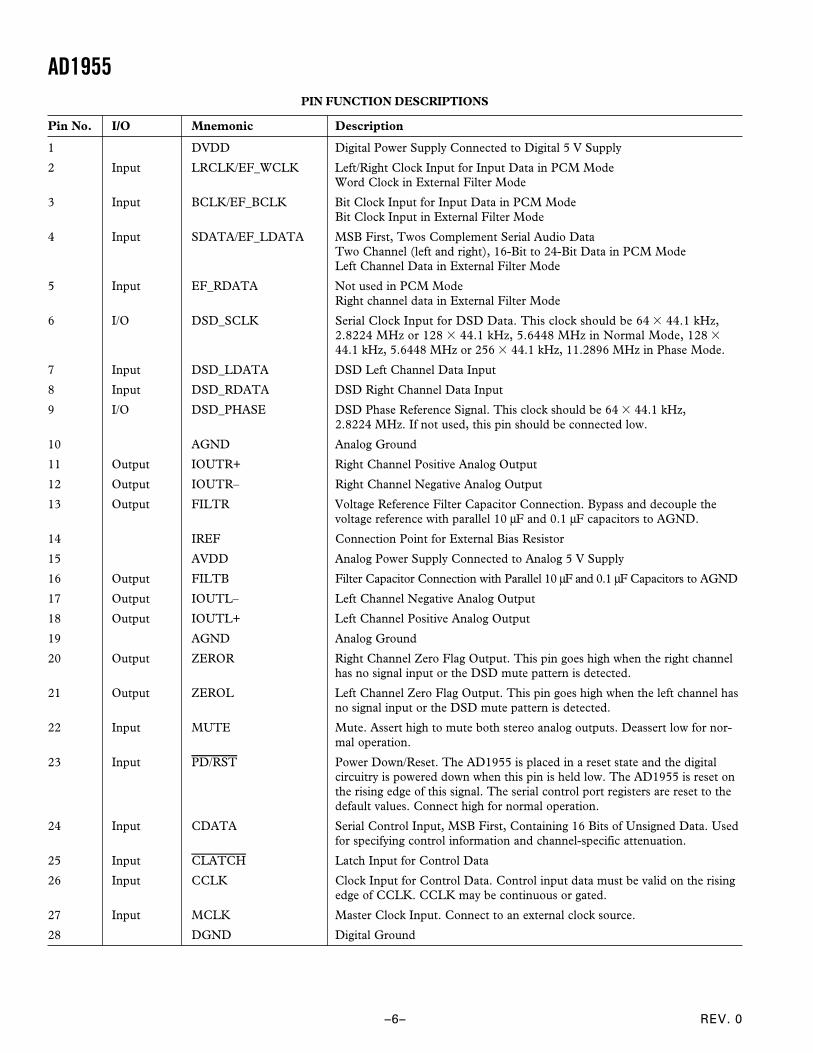
AD1955PIN FUNCTION DESCRIPTIONS
Pin No. I/O Mnemonic Description
1 DVDD Digital Power Supply Connected to Digital 5 V Supply
2 Input LRCLK/EF_WCLK Left/Right Clock Input for Input Data in PCM ModeWord Clock in External Filter Mode
3 Input BCLK/EF_BCLK Bit Clock Input for Input Data in PCM ModeBit Clock Input in External Filter Mode
4 Input SDATA/EF_LDATA MSB First, Twos Complement Serial Audio DataTwo Channel (left and right), 16-Bit to 24-Bit Data in PCM ModeLeft Channel Data in External Filter Mode
5 Input EF_RDATA Not used in PCM ModeRight channel data in External Filter Mode
6 I/O DSD_SCLK Serial Clock Input for DSD Data. This clock should be 64 44.1 kHz,2.8224 MHz or 128 44.1 kHz, 5.6448 MHz in Normal Mode, 128 44.1 kHz, 5.6448 MHz or 256 44.1 kHz, 11.2896 MHz in Phase Mode.
7 Input DSD_LDATA DSD Left Channel Data Input
8 Input DSD_RDATA DSD Right Channel Data Input
9 I/O DSD_PHASE DSD Phase Reference Signal. This clock should be 64 44.1 kHz,2.8224 MHz. If not used, this pin should be connected low.
10 AGND Analog Ground
11 Output IOUTR+ Right Channel Positive Analog Output
12 Output IOUTR– Right Channel Negative Analog Output
13 Output FILTR Voltage Reference Filter Capacitor Connection. Bypass and decouple thevoltage reference with parallel 10 µF and 0.1 µF capacitors to AGND.
14 IREF Connection Point for External Bias Resistor
15 AVDD Analog Power Supply Connected to Analog 5 V Supply
16 Output FILTB Filter Capacitor Connection with Parallel 10 µF and 0.1 µF Capacitors to AGND
17 Output IOUTL– Left Channel Negative Analog Output
18 Output IOUTL+ Left Channel Positive Analog Output
19 AGND Analog Ground
20 Output ZEROR Right Channel Zero Flag Output. This pin goes high when the right channelhas no signal input or the DSD mute pattern is detected.
21 Output ZEROL Left Channel Zero Flag Output. This pin goes high when the left channel hasno signal input or the DSD mute pattern is detected.
22 Input MUTE Mute. Assert high to mute both stereo analog outputs. Deassert low for nor-mal operation.
23 Input PD/RST Power Down/Reset. The AD1955 is placed in a reset state and the digitalcircuitry is powered down when this pin is held low. The AD1955 is reset onthe rising edge of this signal. The serial control port registers are reset to thedefault values. Connect high for normal operation.
24 Input CDATA Serial Control Input, MSB First, Containing 16 Bits of Unsigned Data. Usedfor specifying control information and channel-specific attenuation.
25 Input CLATCH Latch Input for Control Data
26 Input CCLK Clock Input for Control Data. Control input data must be valid on the risingedge of CCLK. CCLK may be continuous or gated.
27 Input MCLK Master Clock Input. Connect to an external clock source.
28 DGND Digital Ground

REV. 0
Typical Performance Characteristics–AD1955
–7–
TPC 1. Pass-Band Response, 8 Mode, 48 kHz Sample Rate
TPC 2. Complete Response, 8 Mode, 48 kHz Sample Rate
TPC 3. 44 kHz Pass-Band Response 4 Mode, 96 kHzSample Rate
TPC 4. Complete Response, 4 Mode, 96 kHz Sample Rate
TPC 5. Pass-Band Response, 2 Mode, 192 kHzSample Rate
TPC 6. Complete Response, 2 Mode, 192 kHzSample Rate

REV. 0–8–
AD1955
TPC 7. DSD Digital Filter Pass Band
TPC 8. DSD Digital Filter Response, Input SampleRate = 2.8224 MHz
TPC 9. FFT Plot, THD + N = –110 dBFS, PCM SR = 48kHz, 0 dBFS @ 1 kHz
TPC 10. FFT Plot, DNR = 121 dBFS (A-Weight), PCMSR = 48 kHz, –60 dBFS @ 1 kHz
TPC 11. FFT Plot, SNR = 121 dBFS (A-Weight), PCMSR = 48 kHz with Zero Input
TPC 12. Linearity, PCM SR = 48 kHz, 0 dBFS to–140 dBFS Input @ 200 Hz
REV. 0
AD1955
–9–
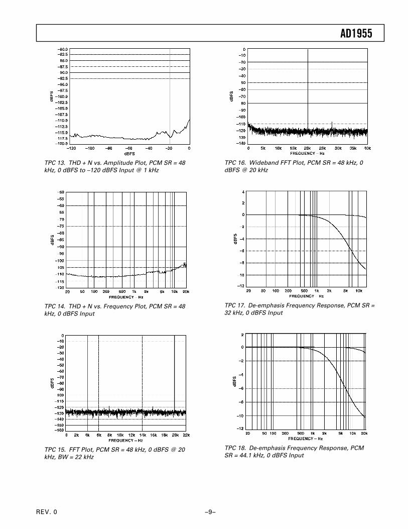
TPC 13. THD + N vs. Amplitude Plot, PCM SR = 48kHz, 0 dBFS to –120 dBFS Input @ 1 kHz
TPC 14. THD + N vs. Frequency Plot, PCM SR = 48kHz, 0 dBFS Input
TPC 15. FFT Plot, PCM SR = 48 kHz, 0 dBFS @ 20kHz, BW = 22 kHz
TPC 16. Wideband FFT Plot, PCM SR = 48 kHz, 0dBFS @ 20 kHz
TPC 17. De-emphasis Frequency Response, PCM SR =32 kHz, 0 dBFS Input
TPC 18. De-emphasis Frequency Response, PCMSR = 44.1 kHz, 0 dBFS Input
REV. 0–10–
AD1955
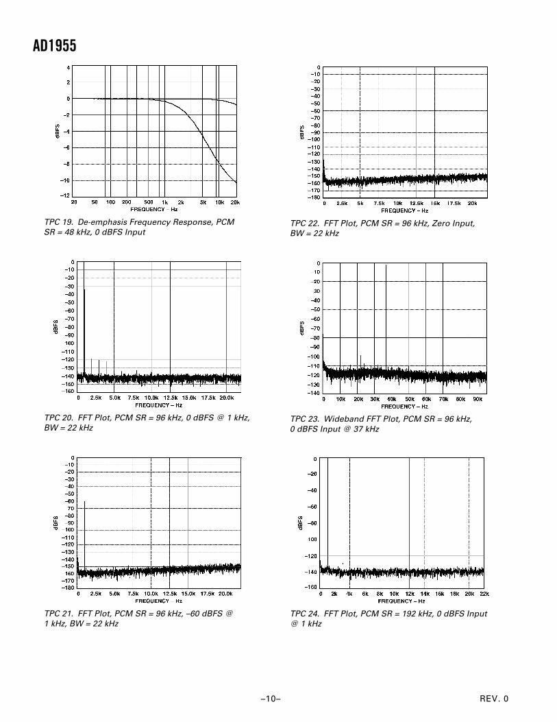
TPC 19. De-emphasis Frequency Response, PCMSR = 48 kHz, 0 dBFS Input
TPC 20. FFT Plot, PCM SR = 96 kHz, 0 dBFS @ 1 kHz,BW = 22 kHz
TPC 21. FFT Plot, PCM SR = 96 kHz, –60 dBFS @1 kHz, BW = 22 kHz
TPC 22. FFT Plot, PCM SR = 96 kHz, Zero Input,BW = 22 kHz
TPC 23. Wideband FFT Plot, PCM SR = 96 kHz,0 dBFS Input @ 37 kHz
TPC 24. FFT Plot, PCM SR = 192 kHz, 0 dBFS Input@ 1 kHz
REV. 0
AD1955
–11–
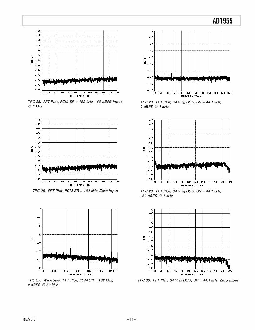
TPC 25. FFT Plot, PCM SR = 192 kHz, –60 dBFS Input@ 1 kHz
TPC 26. FFT Plot, PCM SR = 192 kHz, Zero Input
TPC 27. Wideband FFT Plot, PCM SR = 192 kHz,0 dBFS @ 60 kHz
TPC 28. FFT Plot, 64 fS DSD, SR = 44.1 kHz,0 dBFS @ 1 kHz
TPC 29. FFT Plot, 64 fS DSD, SR = 44.1 kHz,–60 dBFS @ 1 kHz
TPC 30. FFT Plot, 64 fS DSD, SR = 44.1 kHz, Zero Input
REV. 0–12–
AD1955
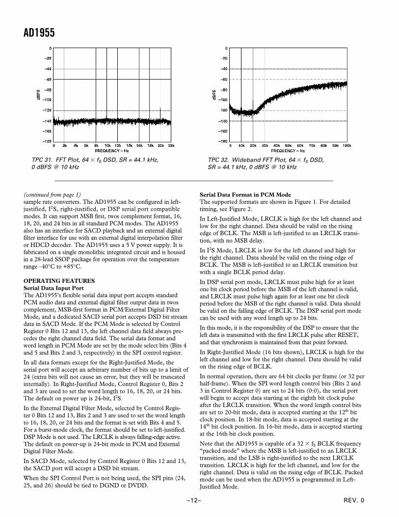
TPC 31. FFT Plot, 64 fS DSD, SR = 44.1 kHz,0 dBFS @ 10 kHz
TPC 32. Wideband FFT Plot, 64 fS DSD,SR = 44.1 kHz, 0 dBFS @ 10 kHz
(continued from page 1)sample rate converters. The AD1955 can be configured in left-justified, I2S, right-justified, or DSP serial port compatiblemodes. It can support MSB first, twos complement format, 16,18, 20, and 24 bits in all standard PCM modes. The AD1955also has an interface for SACD playback and an external digitalfilter interface for use with an external digital interpolation filteror HDCD decoder. The AD1955 uses a 5 V power supply. It isfabricated on a single monolithic integrated circuit and is housedin a 28-lead SSOP package for operation over the temperaturerange –40°C to +85°C.
OPERATING FEATURESSerial Data Input PortThe AD1955’s flexible serial data input port accepts standardPCM audio data and external digital filter output data in twoscomplement, MSB-first format in PCM/External Digital FilterMode, and a dedicated SACD serial port accepts DSD bit streamdata in SACD Mode. If the PCM Mode is selected by ControlRegister 0 Bits 12 and 13, the left channel data field always pre-cedes the right channel data field. The serial data format andword length in PCM Mode are set by the mode select bits (Bits 4and 5 and Bits 2 and 3, respectively) in the SPI control register.
In all data formats except for the Right-Justified Mode, theserial port will accept an arbitrary number of bits up to a limit of24 (extra bits will not cause an error, but they will be truncatedinternally). In Right-Justified Mode, Control Register 0, Bits 2and 3 are used to set the word length to 16, 18, 20, or 24 bits.The default on power up is 24-bit, I2S.
In the External Digital Filter Mode, selected by Control Regis-ter 0 Bits 12 and 13, Bits 2 and 3 are used to set the word lengthto 16, 18, 20, or 24 bits and the format is set with Bits 4 and 5.For a burst-mode clock, the format should be set to left-justified.DSP Mode is not used. The LRCLK is always falling-edge active.The default on power-up is 24-bit mode in PCM and ExternalDigital Filter Mode.
In SACD Mode, selected by Control Register 0 Bits 12 and 13,the SACD port will accept a DSD bit stream.
When the SPI Control Port is not being used, the SPI pins (24,25, and 26) should be tied to DGND or DVDD.
Serial Data Format in PCM ModeThe supported formats are shown in Figure 1. For detailedtiming, see Figure 2.
In Left-Justified Mode, LRCLK is high for the left channel andlow for the right channel. Data should be valid on the risingedge of BCLK. The MSB is left-justified to an LRCLK transi-tion, with no MSB delay.
In I2S Mode, LRCLK is low for the left channel and high forthe right channel. Data should be valid on the rising edge ofBCLK. The MSB is left-justified to an LRCLK transition butwith a single BCLK period delay.
In DSP serial port mode, LRCLK must pulse high for at leastone bit clock period before the MSB of the left channel is valid,and LRCLK must pulse high again for at least one bit clockperiod before the MSB of the right channel is valid. Data shouldbe valid on the falling edge of BCLK. The DSP serial port modecan be used with any word length up to 24 bits.
In this mode, it is the responsibility of the DSP to ensure that theleft data is transmitted with the first LRCLK pulse after RESET,and that synchronism is maintained from that point forward.
In Right-Justified Mode (16 bits shown), LRCLK is high for theleft channel and low for the right channel. Data should be validon the rising edge of BCLK.
In normal operation, there are 64 bit clocks per frame (or 32 perhalf-frame). When the SPI word length control bits (Bits 2 and3 in Control Register 0) are set to 24 bits (0:0), the serial portwill begin to accept data starting at the eighth bit clock pulseafter the LRCLK transition. When the word length control bitsare set to 20-bit mode, data is accepted starting at the 12th bitclock position. In 18-bit mode, data is accepted starting at the14th bit clock position. In 16-bit mode, data is accepted startingat the 16th bit clock position.
Note that the AD1955 is capable of a 32 fS BCLK frequency“packed mode” where the MSB is left-justified to an LRCLKtransition, and the LSB is right-justified to the next LRCLKtransition. LRCLK is high for the left channel, and low for theright channel. Data is valid on the rising edge of BCLK. Packedmode can be used when the AD1955 is programmed in Left-Justified Mode.

REV. 0
AD1955
–13–
Serial Data Format in External Digital Filter ModeIn the External Digital Filter Mode, the AD1955 will acceptup to 24-bit serial, twos complement, MSB-first data from anexternal digital filter, an HDCD decoder, or a general-purposeDSP. If the External Digital Filter Mode is selected by ControlRegister 0, Bits 12 and 13, Pin 2 to Pin 5 are assigned as the wordclock input (EF_WCLK, Pin 2), bit clock input (EF_BCLK,Pin 3), left channel data input (EF_LDATA, Pin 4), and rightchannel data input (EF_RDATA, Pin 5), respectively, to accept8fS (48 kHz), 4fS (96 kHz), or 2fS (196 kHz) oversampled data.
Left and right channel data should be valid on the rising edgeof EF_BCLK. The mode can be set to Left- or Right-Justified.A burst mode BCLK can be used in Left-Justified Mode.
Serial Data Format in SACD ModeIn the SACD Mode, the AD1955 supports both normal modeor phase modulation mode, which are selected by ControlRegister 1, Bit 6. If normal mode is selected, DSD_SCLK,DSD_LDATA, and DSD_RDATA are used to interface withDSD decoder chip. In this mode, the DSD data is clocked inthe AD1955 using the rising edge of DSD_SCLK with a 64fS
rate, 2.8224 MHz. DSD_PHASE pin should be connected LOW.
If Phase Modulation Mode is selected, the DSD_PHASE pin isalso used to interface with the DSD decoder. In this mode, a64fS DSD_PHASE signal is used as a reference signal to receivethe data from the decoder. The DSD data is clocked into theAD1955 with a 128fS DSD_SCLK.
The AD1955 can operate as a master or slave device. In MasterMode, the AD1955 will output DSD_SCLK and DSD_PHASE(if in Phase Modulation Mode) to a DSD decoder and willsupport Normal Mode and Phase Modulation Mode 0. In SlaveMode, the AD1955 will accept DSD_SCLK and DSD_PHASE(if in Phase Modulation Mode) from a DSD decoder and sup-ports all of the normal and phase modulation modes.
When the SACD Port is not being used, the SACD pins (Pins6, 7, 8, and 9) should be tied to a valid logic level. Please notethat there are weak pull-ups (0.6 mA typical) on DSD_SCLKand DSD_PHASE.
Master ClockThe AD1955 must be set to the proper sample rate and masterclock rate using Control Registers 0 and 1. The allowable masterclock frequencies for each interpolation mode are shown below.
In the External Filter Mode, the AD1955 accepts master clockfrequencies depending on the input sample rate as shown below.
In the SACD Mode, the AD1955 accepts a 256fS, 512fS, or768fS Master Clock, where fS is nominally 44.1 kHz. In SlaveMode, by default, the rising edge of DSD_SCLK should coincidewith the rising edge of MCLK. Control Register 1, Bit 2 shouldbe set to 1 if the rising edge of DSD_SCLK coincides with thefalling edge of MCLK. In Master Mode this bit can be used toselect the MCLK edge used to generate the DSD clock outputs.
Zero DetectionWhen the AD1955 detects that the audio input data is continu-ously zero during 1024 LRCLK periods in PCM Mode or 8192LRCLK periods in 8fS External Digital Filter Mode, ZEROL(Pin 21) or ZEROR (Pin 20) is set to active.
When the AD1955 is in SACD Mode, it will detect an SACDmute pattern. If the input bit stream shows a mute pattern forabout 22 ms, the AD1955 will set ZEROL (Pin 21) or ZEROR(Pin 20) to active. The outputs can be set to active high or lowusing Control Register 1, Bit 8.
Reset/Power-DownThe AD1955 will be reset when the PD/RST pin is set low. Thepart may be powered down using Bit 15, Control Register 0.
Audio OutputsActive I/V converters should be used, which will hold the DACoutputs at a constant voltage level. Passive I/V conversion shouldnot be used, since the DAC performance will be seriously degraded.For best THD + N performance over temperature, a referencevoltage of 2.80 V should be used with the I/V converters. For alower parts count, the voltage at FILTR can be used. In thisinstance, THD + N performance at high temperature can beimproved by reducing IREF, with an attendant reduction in gain(linear dependence) and DNR/SNR (square-root dependence).
The AD1955 audio outputs sink a current proportional to theinput signal, superimposed on a steady bias current. The cur-rent-to-voltage (I/V) converters used need to be able to supplythis bias current, as well as the signal current, or a resistor orcurrent source can be used to a positive voltage to null thiscurrent in order to center the range of the I/V converters.
If pull-up resistors are used to bring the output of the I/V convert-ers to 0 V for maximum headroom and THD balance, as shownin the applications circuits, the following equation can be used:
R V V I V RPULLUP SUPPLY BIAS BIAS BIAS I V= [ ] +[ ]– ( )/
PCM Mode
Allowable Master Clock Frequencies ( fS) Nominal InputInterpolation Mode 64 96 128 192 256 384 512 768 Sample Rate (kHz)
48 kHz (INT 8×) Mode • • • 32, 44.1, 48
96 kHz (INT 4×) Mode • • • 88.2, 96
192 kHz (INT 2×) Mode • • • 176.4, 192
External Filter Mode
Allowable Master Clock Frequencies ( fS) Nominal Input Sample RateInput Sample Rate 64 96 128 192 256 384 512 768 (to External Filter) (kHz)
8 × fS • • • 32, 44.1, 48
4 × fS • • • 88.2, 96
2 × fS • • • 176.4, 192

REV. 0–14–
AD1955For example, with the stereo circuits given in Figures 7 through10, this gives:
12 0 2 80 3 24 2 80 2 00 1 98. – . . . . .V V mA V K k[ ] + ( )[ ] = Ω
A 2.00 kΩ resistor is used.
The supply used should be as quiet as possible.
Serial Control PortThe AD1955 has an SPI compatible control port to permit pro-gramming the internal control registers. The SPI control port isa 3-wire serial port. Its format is similar to the Motorola SPIformat except that the input data-word is 16 bits wide. The serialbit clock may be completely asynchronous to the sample rate of theDAC. The following figure shows the format of the SPI signalNote that the CCLK may be continuous or a 16-clock burst.
SPI REGISTER DEFINITIONS
Table I. DAC Control Register 0
Bit Description Value Definition
15 Power-Down 0 Operation1 Powered Down
14 Mute 0 Not Muted1 Muted
13:12 Data Format 00 PCM01 External DF10 SACD Slave11 SACD Master
11:10 Output Format 00 Stereo01 Not Allowed10 Mono Left11 Mono Right
9:8 PCM Sample Rate 00 48 kHz01 96 kHz10 192 kHz11 Reserved
7:6 De-Emphasis Curve 00 NoneSelect 01 44.1 kHz
10 32 kHz11 48 kHz
5:4 PCM/EF Serial Data 00 I2SFormat 01 Right-Justified
10 DSP11 Left-Justified
3:2 PCM/EF Serial Data 00 24 bitsWidth 01 20 bits
10 18 bits11 16 bits
1:0 SPI Register Address 00
Default = 0
Table II. DAC Control Register 1
Bit Description Value Definition
10:9 MCLK Mode 00 256 fS
01 512 fS
10 768 fS
11 Reserved
8 Zero Flag Polarity 0 Active High1 Active Low
7 SACD Bit Rate 0 64 fS
1 128 fS
6 SACD Mode 0 Normal1 Phase Mode
5:4 SACD Phase Select 00 Phase 001 Phase 110 Phase 211 Phase 3
3 SACD Bit Inversion 0 Normal1 Inverted
2 SACD MCLK to 0 Rising EdgeBCLK Phase 1 Falling Edge
1:0 SPI Register Address 01
Default = 0
Table III. DAC Volume Registers
Bit Description Value Definition
14-Bit15:2 Volume Unsigned
1:0 SPI Register Address 10 Left Volume11 Right Volume
Default = Full Volume

REV. 0
AD1955
–15–
1/fS
NOTES1. DSP MODE DOES NOT IDENTIFY CHANNEL.2. LRCLK NORMALLY OPERATES AT fS EXCEPT FOR DSP MODE, WHICH IS 2 fS.3. BCLK FREQUENCY IS NORMALLY 64 LRCLK BUT MAY BE OPERATED IN BURST MODE.
LRCLK
BCLK
SDATA
LRCLK
BCLK
SDATA
LRCLK
BCLK
SDATA
LRCLK
BCLK
SDATA
LEFT CHANNEL
LEFT CHANNEL
LEFT CHANNEL
RIGHT CHANNEL
RIGHT CHANNEL
RIGHT CHANNEL
I2S MODE –16 TO 24 BITS PER CHANNEL
RIGHT-JUSTIFIED MODE – SELECT NUMBER OF BITS PER CHANNEL
LEFT-JUSTIFIED MODE – 16 TO 24 BITS PER CHANNEL
DSP MODE – 16 TO 24 BITS PER CHANNEL
MSB
MSB
MSB
MSB
MSB
MSB
MSB
MSB LSB
LSB
LSB
LSBLSB
LSB
LSB
Figure 1. Supported Serial Data Formats
tDLS
BCLK
L/RCLK
SDATALEFT-JUSTIFIED
MODE
SDATARIGHT-JUSTIFIED
MODELSB
SDATAI2S-JUSTIFIED
MODE
tDBH tDBP
tDBL
tDDS
MSB MSB-1
tDDH
tDDS
MSB
tDDH
tDDS tDDS
tDDH tDDH
MSB
8-BIT CLOCKS(24-BIT DATA)
12-BIT CLOCKS(20-BIT DATA)
16-BIT CLOCKS(16-BIT DATA)
Figure 2. Serial Data Port Timing

REV. 0–16–
AD1955
DSD_DATA
DSD_BCLK
DSD_DATA
DSD_BCLK
DSD_PHASE_0
DSD_PHASE_1
DSD_PHASE_2
DSD_PHASE_3
D0 D1
D0 D0
NORMALMODE
PHASEMOD
MODE
Figure 3. DSD Modes
DSD_PHASE
DSD_SCLK
DSD_LDATA, DSD_RDATA
tDPHS
tDSKP
tDSKH
tDSKLtDSDS
tDSDH
Figure 4. DSD Serial Port Timing
CLATCH
CCLK
CDATA D15 D14 D0
tCLKL
tCLKH
tCDS
tCDH
tCLATCHH
Figure 5. Serial Control Port Timing

REV. 0
AD1955
–17–
DVDD AVDD
L2600Z
L3600Z
C20.1F
C10.1F
MCLK
EF_RDATA
SDATA/EF_LDATABCLK/EF_BCLK
LRCLK/EF_WCLK
DSD_PHASE
DSD_RDATA
DSD_LDATA
DSD_SCLK
CDATA
CCLK
MUTE
ZERORZEROL
PD/RST
IOUTL+
IOUTL–
IOUTR+
IOUTR–
DGND AGND1 AGND2
IREF
FILTB
FILTR
DVDD AVDD
AD1955
U1
AVDD
OR
VREF VBIAS
VREFA
VREFA2.80V
C440.1F
C4347F
R572.80k
R562.21k
+
CONNECT VBIAS TO VREFA FOR BEST PERFORMANCEOR VREF FOR LOWER PARTS COUNT
600ZL1
R12.49k
C30.1F
C410F
C50.1F
C647F
VREF2.39V
++
MCLK
RDATA
SDATA
BCLKLRCLK
DSD_PHASE
DSD_RDATA
DSD_LDATA
DSD_SCLK
CDATA
CLATCHCCLK
MUTE
ZERORZEROL
IOUTL+
IOUTL–
IOUTR+
IOUTR–
PD/RST
CLATCH
Figure 6. DAC Power Supply and Bypass
REV. 0–18–
AD1955
+
+
AD797
+12V
0.1F
0.1F
4.7F
4.7F
OP AMP BYPASSDUPLICATE FOR EACH PART
–12V
COMP
OUT
NL–NL+
AD797
U2-A
COMP
OUT
NL–
U3-A
NL+
AD797
G
–
+
XL
R M
AL
E
J1
LEFTDIRECTOUT6VRMS
VBIAS
IOUTL–
IOUTL+
C9100pF
C8OPEN
C7OPEN
R22.00k
R32.00k
12V
R4402
R52.00k
R6100
C10100pF
R7100
C11100pF
R82.00k
C12390pF
R91.00k
R101.00k
R111.00k
R121.00k
C14470pF
C13470pF
–3dB at 100 kHz
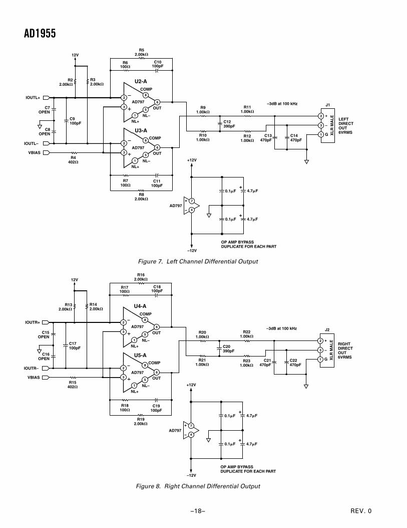
Figure 7. Left Channel Differential Output
+
+
AD797
+12V
0.1F
0.1F
4.7F
4.7F
OP AMP BYPASSDUPLICATE FOR EACH PART
–12V
COMP
OUT
NL–NL+
AD797
U4-A
COMP
OUT
NL–
U5-A
NL+
AD797
G
–
+
XL
R M
AL
EJ2
RIGHTDIRECTOUT6VRMS
VBIAS
IOUTR–
IOUTR+
C17100pF
C16OPEN
C15OPEN
R132.00k
R142.00k
12V
R15402
R162.00k
R17100
C18100pF
R18100
C19100pF
R192.00k
C20390pF
R201.00k
R211.00k
R221.00k
R231.00k
C22470pF
C21470pF
–3dB at 100 kHz
Figure 8. Right Channel Differential Output

REV. 0
AD1955
–19–
COMP
OUT
NL–NL+
AD797
U6-A
COMP
OUT
NL–
U7-A
NL+
AD797
OUT
NL–NL+
AD797
COMP
U8-A
+
+
AD797
+12V
VBIAS
0.1F
0.1F
4.7F
4.7F
OP AMP BYPASSDUPLICATE FOR EACH PART
–12V
IOUTL–
IOUTL+
C24OPEN
C23OPEN
C25100pF
R242.00k
R252.00k
12VR27
2.00k
R28100
C26100pF
R29100
C27100pFR30
2.00k
R31681
R32681
R33226
C285.6nF
C295.6nF
R36226
R35324
R34324
C312.7nF
C302.7nF
R37100
R38332 J3
–3dB at 75 kHz
C323.9nF
R39OPEN
LEFTFILTEROUT2VRMS
R26402
Figure 9. Left Channel Single-Ended Output
COMP
OUT
NL–NL+
AD797
U9-A
COMP
OUT
NL–
U10-A
NL+
AD797
OUT
NL–NL+
AD797
COMP
U11-A
+
+
+12V
AD797
VBIAS
0.1F
0.1F
4.7F
4.7F
OP AMP BYPASSDUPLICATE FOR EACH PART
–12V
IOUTR–
IOUTR+
C34OPEN
C33OPEN
C35100pF
R402.00k
R412.00k
12VR43
2.00k
R44100
C36100pF
R45100
C37100pFR46
2.00k
R47681
R48681
R49226
C385.6nF
C395.6nF
R52226
R51324
R50324
C412.7nF
C402.7nF
R53100
R54332 J4
–3dB at 75 kHz
C423.9nF
R55OPEN
RIGHTFILTEROUT2VRMS
R42402
Figure 10. Right Channel Single-Ended Output
REV. 0–20–
AD1955
+
+
AD797
+12V
0.1F
0.1F
4.7F
4.7F
OP AMP BYPASSDUPLICATE FOR EACH PART
–12V
COMP
OUT
NL–NL+
AD797
U2-A
COMP
OUT
NL–
U3-A
NL+
AD797
G
–
+
XL
R M
AL
E
J1
MONODIRECTOUT6VRMS
NOTE REVERSE POLARITYOF RIGHT CHANNEL OUTPUTS
VBIAS
IOUTL–
IOUTR–
IOUTR+
IOUTL+
C9100pF
C8OPEN
C7OPEN
R21.00k
R31.00k
12V
R4402
R51.00k
R6100
C10100pF
R7100
C11100pF
R81.00k
C12390pF
R91.00k
R101.00k
R111.00k
R121.00k
C14470pF
C13470pF
–3dB at 100 kHz
SET CONTROL REGISTER 0, BITS 11:10TO SELECT LEFT OR RIGHT CHANNEL
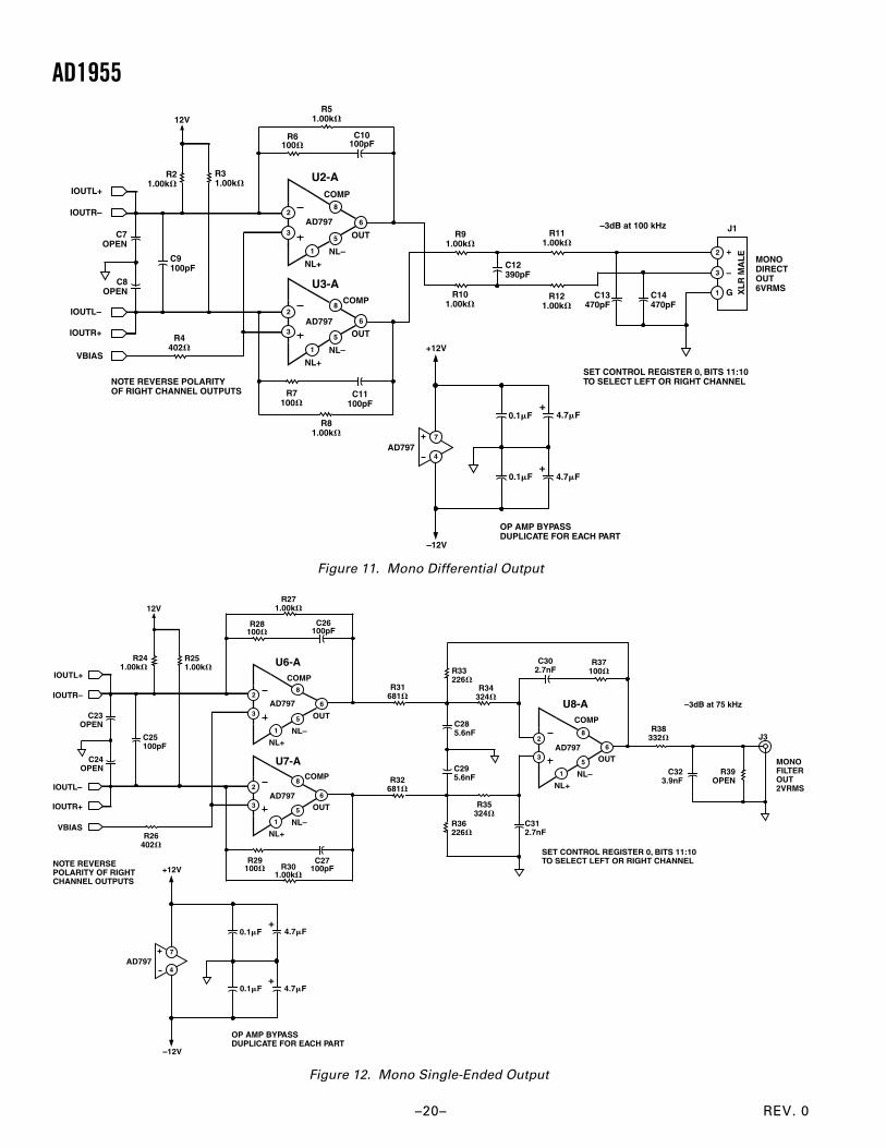
Figure 11. Mono Differential Output
COMP
OUT
NL–NL+
AD797
U6-A
COMP
OUT
NL–
U7-A
NL+
AD797
OUT
NL–NL+
AD797
COMP
U8-A
+
+
AD797
+12V
0.1F
0.1F
4.7F
4.7F
OP AMP BYPASSDUPLICATE FOR EACH PART
–12V
VBIAS
IOUTL–
IOUTR–
IOUTR+
IOUTL+
C24OPEN
C23OPEN
C25100pF
R26402
NOTE REVERSEPOLARITY OF RIGHTCHANNEL OUTPUTS
R241.00k
R251.00k
12VR27
1.00k
R28100
C26100pF
R29100
C27100pFR30
1.00k
R31681
R32681
R33226
C285.6nF
C295.6nF
R36226
R35324
R34324
C312.7nF
C302.7nF
R37100
R38332 J3
–3dB at 75 kHz
C323.9nF
R39OPEN
MONOFILTEROUT2VRMS
SET CONTROL REGISTER 0, BITS 11:10TO SELECT LEFT OR RIGHT CHANNEL
Figure 12. Mono Single-Ended Output

REV. 0
AD1955
–21–
OUTLINE DIMENSIONSDimensions shown in millimeters
28-Lead Shrink Small Outline Package (SSOP)(RS-28)
0.250.09
0.950.750.55
840
0.05MIN
1.851.751.652.00 MAX
0.380.22 SEATING
PLANE
0.65BSC
0.10COPLANARITY
28 15
141
10.5010.209.90
5.605.305.00
8.207.807.40
COMPLIANT TO JEDEC STANDARDS MO-150AH

–22–

–23–

C02
805–
0–10
/02(
0)P
RIN
TE
D IN
U.S
.A.
–24–