a high-speed 1t-4mtj mram voltage offsetself-reference
TRANSCRIPT

11-2
A high-density and high-speed 1T-4MTJ MRAMwith Voltage Offset Self-Reference Sensing Scheme
Hiroaki Tanizaki ', Takaharu Tsuji 2, Jun Otani 2, Yuichiro Yamaguchi 2 Yasumitsu Murai ',Haruo Furuta 2,Shuichi Ueno 2, Tsukasa Oishi 2, Masanori Hayashikoshi 2, and Hideto Hidaka 2
1 Renesas Design Corporation, 4-1 Mizuhara, Itami, Hyogo 664-0005, Japan Tel: 072-784-73312Renesas Technology Corporation, 4-1 Mizuhara, Itami, Hyogo 664-0005, Japan Tel:072-784-7336
Abstract A high-density and high-speed memory cellnamed 1-Transistor 4-Magnetic Tunnel Junction(1T-4MTJ) has been proposed for Magnetic RandomAccess Memory (MRAM). The new 1T-4MTJ cell hasbeen successfully demonstrated by a 1Mb MRAM testdevice, using a 130nm CMOS process. The sensingscheme of a Self-Reference Sense amplifier withVoltage offset (SRSV) enables high-speed memoryoperation (access time) of tAC=56nsec and5OMHzg4cycle.
I. INTRODUCTION
Although MRAM has favorable attributes for auniversal memory like non-volatility, low-voltageoperation, high-speed access, and unlimited write/readendurance, it lacks advantage in cost because currentlyavailable 1 T-1MTJ cell is larger than DRAM and flashmemory cells. To realize a high-density MRAM array, across-point MRAM cell has been proposed. However,since the sneak current between BL (bit-line) andadjacent BL degrades the signal margin, read-out speedis very slow [ 1 ] [2] [3].A novel 1T-4MTJ cell consists of one transistor and
4MTJ elements connected in parallel alongside one BL.1T-4MTJ cell solves the sneak current problem, andrealizes a smaller cell size as well. It also achieves fastread access by a low memory cell resistance arising fromthe parallel-connected cell structure.
II. ARCHITECTURE OF 1T-4MTJ MRAM
A. Memory cell structureFigure 1 (a) shows the cross-sectional structure of
IT-IMTJ cell. LI (Local Interconnect) is required tobypass a WWL (Write Word Line), resulting in largercell area. Figure 1 (b) is the proposed 1T-4MTJ cell,which places four MTJ elements in parallel. LI is alsorequired in 1T-4MTJ cell, but the area penalty is reducedby sharing LI with four MTJs. 1T-4MTJ cell realizes thecell area reduction by 4400 compared with that of1T-1MTJ cell.
Figure 2 is the SEM photograph of the cell fabricatedby 130nm design, where 4MTJ elements, LI and LV(Local internal connect Via) are shown.
Fig.2. SEM photograph of 1T-4MTJ.
(2nd Cu) BLLI MTJ
(lst Cu) LVWWL
Psub (SL)
BLLI L 1 a MTJ
LV llWWLO WWL1 WWL2 WWL3
Psu (SL)
WL WL WWL: Write Word LineWL: Read Word Line
Cell sizeratio 1.00 0.56
Read access time 10-20 nsec 50-60 nsec
(a) IT- IMTJ cell (b) IT- 4MTJ cell
Fig. 1. MRAM memory cells.
B. Read-out schemeIT-IMTJ usually applies the sensing method of
comparing the selected cell and the reference cell.1T-4MTJ cell cannot use the reference cell since 4MTJelements produce 16(24) combinations. The read-out of1T-4MTJ adopts a new self-reference sensing schemewhich completes by 4 cycles. Figure 3 describes theread-out flow and the state of 4MTJs, where WWLO isselected.(1) 1st read: By activating WL, the current at BL flowsthrough 4MTJs, and the BL current is sensed.(2) Hi write: Hi data (data" 1") is always written to theselected MTJ by activating WWLO.
0-7803-9735-5/06/$20.00 ©2006 IEEE 303

The write operation to one of4MTJ is performed by themagnetic field generated at the intersection between BLand WWLn (n=0-3).(3) 2nd read: By re-activating WL, the current at BLflows through 4MTJs ,and the BL current is sensed. Andthe current change(equivalent to the resistance change)between 1st read, and 2nd read is detected.When data"0" is stored data, the resistance change is10.0% (400 o: MR (Magnetic Resistance Rate) of oneMTJ element), while the resistance does not change incase of data"1". The read-out amplifier does not workwithout resistance change. Then, the circuit of attachingvoltage offset is implemented. Figure 4 shows thevoltage offset on the reference node (RSAO) generated atthe end of 1st read.(4) write back: when stored data is "0", data"0" is writtenby activating WWLO. When stored data is " 1", nooperation happens.
Select MTJ Select MTJ
WWLO WWL1 WWL2 WWL3
0 x x xMTJO MJ1M MTJ2 MTJ3
3x xIxI
I x x xStored data=0
ICmx x paresComp ares I
WWLO WWL1 WWL2 WWL3
MTJO MrJi MTJ2 MTJ3
I x x x
Stored data=
IE3XI CCompares I
amplifier. This paper proposes a novel Self-ReferenceSense amplifier with Voltage offset (SRSV) by thecharge sharing principle. This voltage offset should beadjusted corresponding to the resistance change mainlydetermined by MR of one MTJ. For this purpose,the variable voltage offset circuit is introduced byapplying the tuning voltage(see Fig. 5).
During 1st read, a VNG node is constant voltage(VCC>VNG), and the voltage ofBL is kept at VNG-Vth.1T-4MTJ cell current is transformed to Vgs voltage onQND transistor gate, corresponding to Ids current (=cellcurrent of stored data "0" or "1"). Capacity Cl and C2are charged to Vgs. Next, 4I is turned off and +2 is turnon just before the end of 1st read. Tuning voltage isapplied to C3 when 4I is on. The charge sharing betweenC2 and C3 is proceeded when +2 is on (4I is off).Hereby, the voltage of Vgs-1/2AV is induced on RSAO.Exact voltage offset is achieved by trimming the tuningvoltage. The capacity ratio of C2 to C3 is set 10 tol.Offset voltage is finely adjusted by the step for 1/11 ofthe tuning voltage. AV is the voltage difference on SAObetween data"l" and data"0".
2nd read is performed after Hi write cycle. Ids current(=cell current of data"1".) flows through QND transistor,which gate is biased at Vgs. Vgs voltage defined at 1stread is held by C1. Then, the drain voltage of QNDtransistor (=SAO) is varied according to stored data "0"or " 1". The relation between stored data and SAO/RSAOis summarized below.
Stored data"0" SAO=Vgs-AV < RSAO=Vgs- 1/2AVStored data" 1": SAO=Vgs > RSAO=Vgs-1/2AV
Hi: Hi data write, Low:Low data write, Non:No write
(a) Read-out flow (b) Stored data=0 (c) Stored data=1
Fig.3. 4-cycle read-out flow and state of 4MTJs.
SAO
t1=ONcD)2=OFF
Volt
t1=OFFc)2=ON
%4 - --- lp
RSAO Vgs SAO(stored data=l)
tage Offset 1 /2AVk ~~~~~1/2AV
SAO stored data=O)
'1st read to 2nd read p
Fig.4. Voltage offset for 1T-4MTJ cell.
C. SRSVRead-out schemeA self-reference sensing is reported for IT-IMTJ
cell[4], using unbalanced transistors of the read-out
Icell ... ...............................
1
_-10:11 Tunmng:XC2 XC3 voltage:
......................................:
Voltage Offset circuit.
MTJ)
SL
Fig.5. Self-reference sense amplifier with voltage offset (SRSV).
304
I1st read
Hi write
2nd read
write back
END
arator
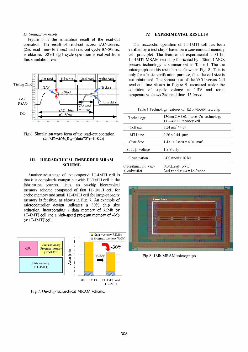
D. Simulation resultFigure 6 is the simulation result of the read-out
operation. The result of read-out access tAC=56nsec(2nd read time=16.2nsec) and read-out cycle tC=80nsecis obtained. 5OMHzg4 cycle operation is realized fromthis simulation result.
Timing CLK .1/A .. 0tidt
X t !< ~~~RSAO --------------
SAORSAO Low data
RYb ~~~~~tAC=56ns =16.2nLDQ tC=80ns
Fig.6. Simulation wave form of the read-out operation.(@ MR=400 o,RMTJ(data"O")=40KQ)
III. HIERARCHICAL EMBEDDED MRAMSCHEME
Another advantage of the proposed 1T-4MTJ cell isthat it is completely compatible with IT-1MTJ cell in thefabrication process. Thus, an on-chip hierarchicalmemory scheme composed of fast IT-IMTJ cell forcache memory and small 1T-4MTJ cell for large-capacitymemory is feasible, as shown in Fig. 7. An example ofmicrocontroller design indicates a 300 chip sizereduction, incorporating a data memory of 32Mb by1T-4MTJ cell and a high-speed program memory of 4Mbby 1T-1MTJ cell.
9E]Data memory(32Mb)
9 Program memory(4M
Cache memory 8 =37fCU Program memo{ry t 6_ ,l
z 5_ ~~1T-4MTJ
Data memory ¢3(1IT-4MTJ) 2_
_
IV. EXPERIMENTAL RESULTS
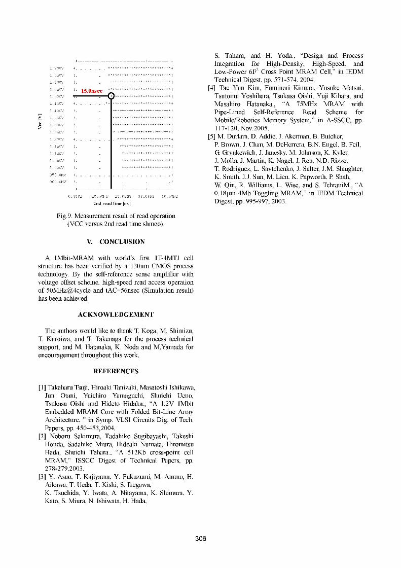
The successful operation of 1T-4MTJ cell has beenverified by a test chip.( based on a conventional memorycell principle). The features of experimental 1 M bit1T-4MTJ MRAM test chip fabricated by 130nm CMOSprocess technology is summarized in Table 1. The diemicrograph of this test chip is shown in Fig. 8. This isonly for a basic verification purpose, thus the cell size isnot minimized. The shmoo plot of the VCC versus 2ndread-out time shown in Figure 9, measured under thecondition of supply voltage at 1.5V and roomtemperature, shows 2nd read time= 1 5.Onsec.
Table 1 Technology features of lMb-MRAM test chip.
Technology 13Onm CMOS, 4Level Cu technologyIT - 4MTJ memory cell
Cell size 3.24 ,um2/ 4 bit
MTJ size 0.26 x 0.44 ,tm2
Core Size 1.431 x 2.820 = 4.04 mm2
Supply Voltage 1.5 V only
Organization 64K word x 16 bit
Operating Frequency 5OMHz 44 cycle(read/write) 2nd read time=15.Onsec
[b)
Fig. 8. 1Mb MRAM micrograph.
all IT-IMTJ IT-IMTJ and1T-4MTJ
Fig.7. On-chip hierarchical MRAM scheme.
305
.650V
15.Onlsec
- .-- - *-
+00 10*ON 20******
I n read time **9
S. Tahara, and H. Yoda., "Design and ProcessIntegration for High-Density, High-Speed, andLow-Power 6F2 Cross Point MRAM Cell," in IEDMTechnical Digest, pp. 571-574, 2004.
[4] Tae Yun Kim, Fuminori Kimura, Yusuke Matsui,Tsutomu Yoshihara, Tsukasa Oishi, Yuji Kihara, andMasahiro Hatanaka., "A 75MHz MRAM withPipe-Lined Self-Reference Read Scheme forMobile/Robotics Memory System," in A-SSCC, pp.117-120, Nov.2005.
[5] M. Durlam, D. Addie, J. Akerman, B. Butcher,P. Brown, J. Chan, M. DeHerrera, B.N. Engel, B. Feil,G. Grynkewich, J. Janesky, M. Johnson, K. Kyler,J. Molla, J. Martin, K. Nagel, J. Ren, N.D. Rizzo,T. Rodriguez, L. Savtchenko, J. Salter, J.M. Slaughter,K. Smith, J.J. Sun, M. Lien, K. Papworth, P. Shah,W. Qin, R. Williams, L. Wise, and S. TehraniM., "A0.18ptm 4Mb Toggling MRAM," in IEDM TechnicalDigest, pp. 995-997, 2003.
Fig.9. Measurement result ofread operation(VCC versus 2nd read time shmoo).
V. CONCLUSION
A lMbit-MRAM with world's first 1T-4MTJ cellstructure has been verified by a 130nm CMOS processtechnology. By the self-reference sense amplifier withvoltage offset scheme, high-speed read access operationof 5OMHzg4cycle and tAC=56nsec (Simulation result)has been achieved.
ACKNOWLEDGEMENT
The authors would like to thank T. Koga, M. Shimizu,T. Kuroiwa, and T. Takenaga for the process technicalsupport, and M. Hatanaka, K. Noda and M.Yamada forencouragement throughout this work.
REFERENCES
[1] Takaharu Tsuji, Hiroaki Tanizaki, Masatoshi Ishikawa,Jun Otani, Yuichiro Yamaguchi, Shuichi Ueno,Tsukasa Oishi and Hideto Hidaka., "A 1.2V IMbitEmbedded MRAM Core with Folded Bit-Line ArrayArchitecture, " in Symp. VLSI Circuits Dig. of Tech.Papers, pp. 450-453,2004.
[2] Noboru Sakimura, Tadahiko Sugibayashi, TakeshiHonda, Sadahiko Miura, Hideaki Numata, HiromitsuHada, Shuichi Tahara., "A 512Kb cross-point cellMRAM," ISSCC Digest of Technical Papers, pp.278-279,2003.
[3] Y. Asao, T. Kajiyama, Y. Fukuzumi, M. Ammo, H.Aikawa, T. Ueda, T. Kishi, S. Ikegawa,K. Tsuchida, Y. Iwata, A. Nitayama, K. Shimura, Y.Kato, S. Miura, N. Ishiwata, H. Hada,
306