a hybrid electromagnetic bandgap (ebg) power plane with
TRANSCRIPT

1
WEMTEC Inc.
WEMTEC Inc. 10-29-07 2007 EPEP Presentation Rev A
A Hybrid Electromagnetic Bandgap (EBG) Power Plane with Discrete Inductors for
Broadband Noise Suppression
Will McKinzieWEMTEC, Inc., PO Box 446, Fulton, MD 20759
Email: [email protected]: (301)442-7030 Fax: (301) 776-7979
Poster presentation at the IEEE 16th Topical Meeting on Electrical Performance of Electronic Packaging,Atlanta, GA Oct 29-31, 2007

2
WEMTEC Inc.
WEMTEC Inc. 10-29-07 2007 EPEP Presentation Rev A
Outline
• Purpose and Applications of Hybrid EBG Structures
• Motivation for an Improved EBG Structure
• Background – What is a Hybrid EBG Structure?
• Hybrid EBG Structure Using Discrete Inductors
- Prototype Hardware
- S Parameter Measurements
- 1D Dispersion Equation
- Formulas for Cutoff Frequency
- Impedance Parameter Measurements
• Conclusions
3
WEMTEC Inc.
WEMTEC Inc. 10-29-07 2007 EPEP Presentation Rev A
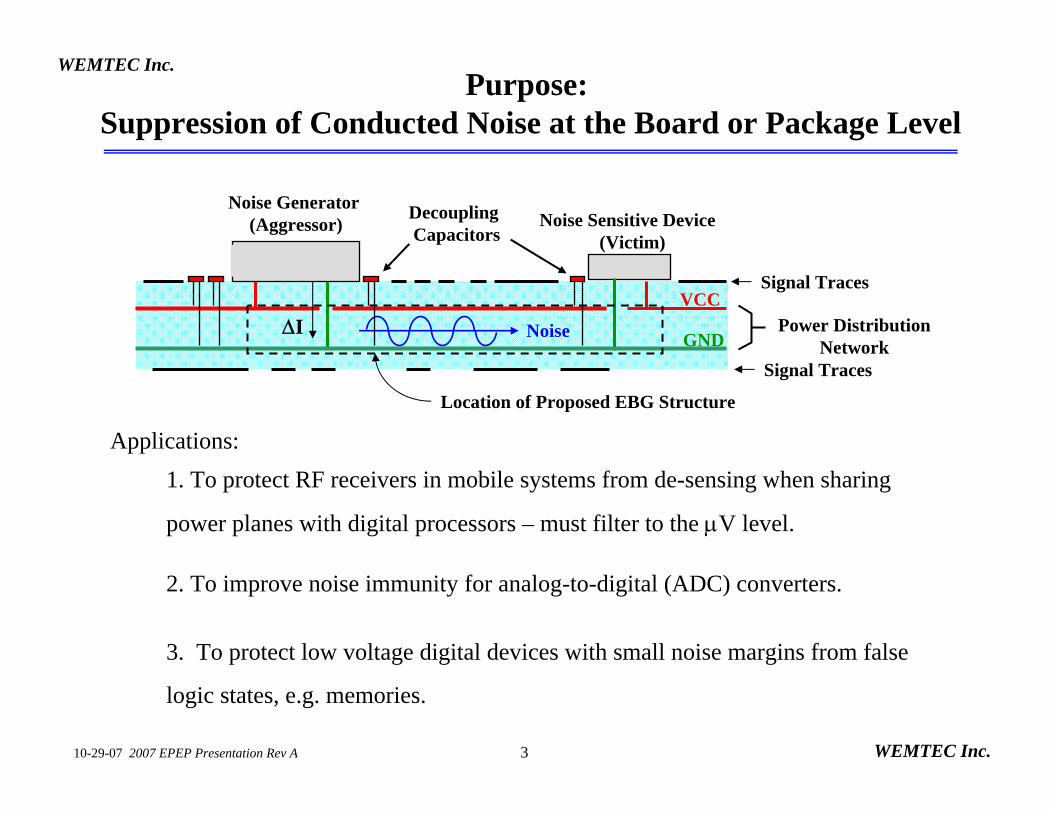
Purpose:Suppression of Conducted Noise at the Board or Package Level
1. To protect RF receivers in mobile systems from de-sensing when sharing
power planes with digital processors – must filter to the µV level.
Noise
Noise Sensitive Device(Victim)
Signal Traces
Power DistributionNetwork
VCC
GND
DecouplingCapacitors
Noise Generator(Aggressor)
∆I
Location of Proposed EBG Structure
Signal Traces
2. To improve noise immunity for analog-to-digital (ADC) converters.
3. To protect low voltage digital devices with small noise margins from false
logic states, e.g. memories.
Applications:
4
WEMTEC Inc.
WEMTEC Inc. 10-29-07 2007 EPEP Presentation Rev A
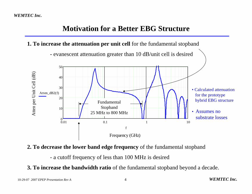
1. To increase the attenuation per unit cell for the fundamental stopband
- evanescent attenuation greater than 10 dB/unit cell is desired
2. To decrease the lower band edge frequency of the fundamental stopband
- a cutoff frequency of less than 100 MHz is desired
3. To increase the bandwidth ratio of the fundamental stopband beyond a decade.
0.01 0.1 1 100
10
20
30
40
50
Frequency (GHz)
Atte
n pe
r Uni
t Cel
l (dB
)
Atten_dB2 f( )
f
Motivation for a Better EBG Structure
FundamentalStopband
25 MHz to 800 MHz
• Calculated attenuationfor the prototype hybrid EBG structure
• Assumes no substrate losses

5
WEMTEC Inc.
WEMTEC Inc. 10-29-07 2007 EPEP Presentation Rev A
Background: What is a Hybrid EBG Structure?
Inductive Grid EBG Structures: Power plane is comprised of a 2D grid of etched TL networks.
Patches
Printed High-Zo TL
Arrays of Resonant Vias: Periodic array of vias exists between the power and ground planes.
Pwr plane
Gnd planeP
Hybrid EBG Structure:Unit Cell Equivalent Circuit
Each Unit Cell Combines aResonant Via + High-Impedance TL
x
yz
Ref: Will McKinzie, 2006 IEEE EPEP Conf., Oct 23-25, 2006, Scottsdale, AZ, pp. 51-54
6
WEMTEC Inc.
WEMTEC Inc. 10-29-07 2007 EPEP Presentation Rev A
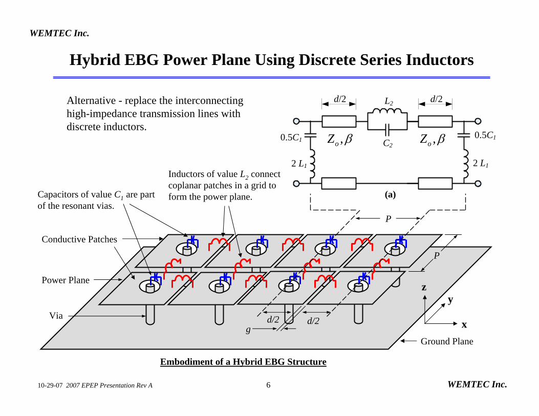
2 L1
0.5C1 C2
L2d/2 d/2
0.5C1
2 L1
Hybrid EBG Power Plane Using Discrete Series Inductors
,oZ β
Embodiment of a Hybrid EBG Structure
Ground Plane
Power Plane
x
yz
Capacitors of value C1 are part of the resonant vias.
Inductors of value L2 connect coplanar patches in a grid to form the power plane. (a)
Via
P
g
Conductive Patches
P
d/2d/2
,oZ β
Alternative - replace the interconnecting high-impedance transmission lines with discrete inductors.
7
WEMTEC Inc.
WEMTEC Inc. 10-29-07 2007 EPEP Presentation Rev A
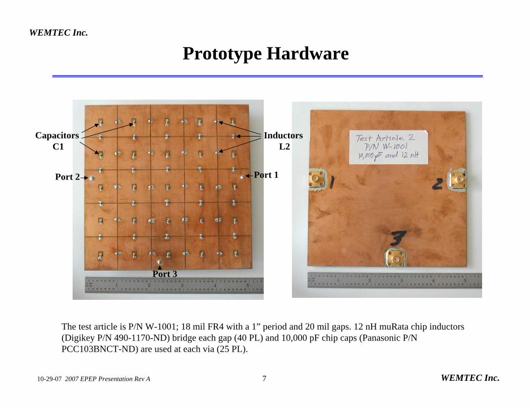
Prototype Hardware
The test article is P/N W-1001; 18 mil FR4 with a 1” period and 20 mil gaps. 12 nH muRata chip inductors (Digikey P/N 490-1170-ND) bridge each gap (40 PL) and 10,000 pF chip caps (Panasonic P/N PCC103BNCT-ND) are used at each via (25 PL).
Port 1Port 2
Port 3
InductorsL2
CapacitorsC1
8
WEMTEC Inc.
WEMTEC Inc. 10-29-07 2007 EPEP Presentation Rev A
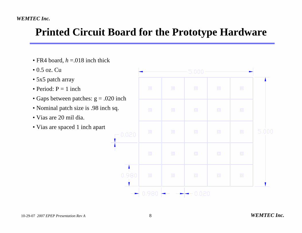
Printed Circuit Board for the Prototype Hardware
• FR4 board, h =.018 inch thick• 0.5 oz. Cu• 5x5 patch array• Period: P = 1 inch• Gaps between patches: g = .020 inch• Nominal patch size is .98 inch sq.• Vias are 20 mil dia.• Vias are spaced 1 inch apart
9
WEMTEC Inc.
WEMTEC Inc. 10-29-07 2007 EPEP Presentation Rev A
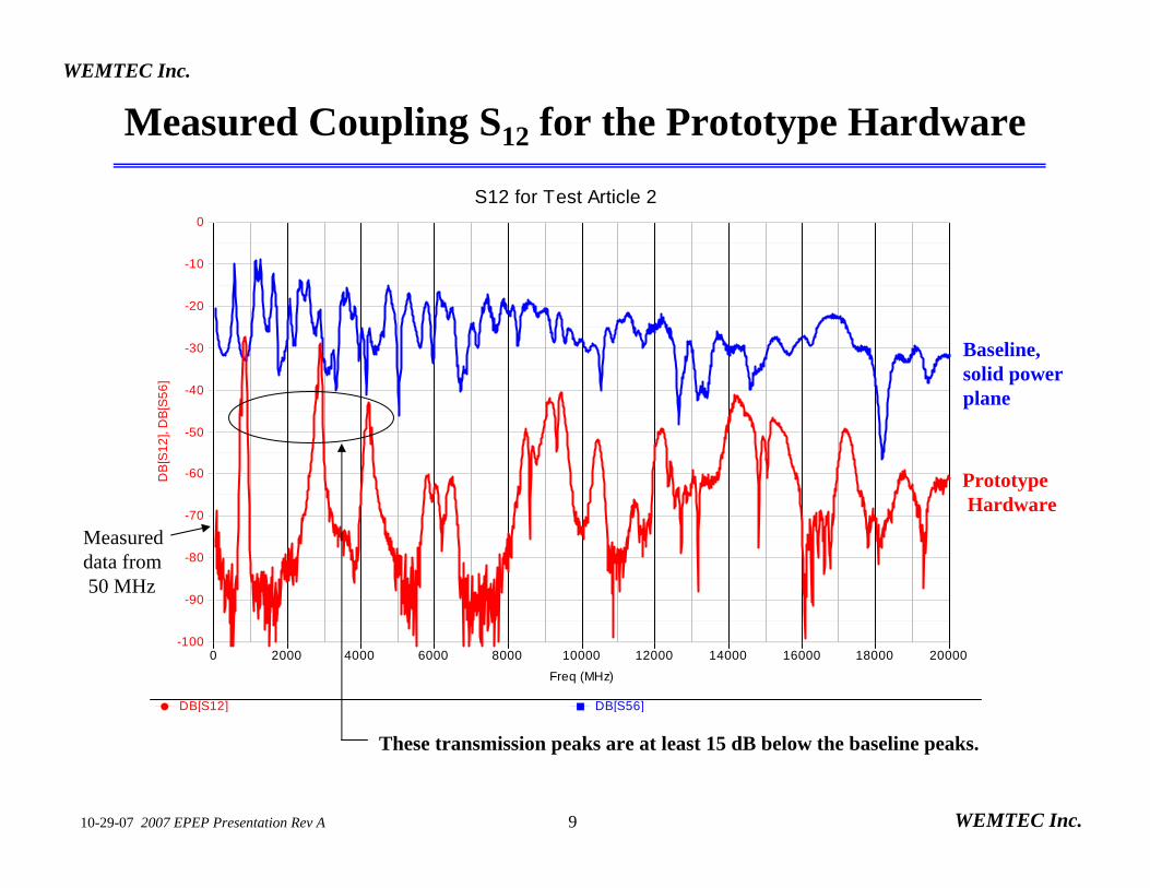
Measured Coupling S12 for the Prototype HardwareD
B[S
12],
DB
[S56
]
-100
-90
-80
-70
-60
-50
-40
-30
-20
-10
0
Freq (MHz)
0 2000 4000 6000 8000 10000 12000 14000 16000 18000 20000
S12 for Test Article 2
DB[S12] DB[S56]
Baseline,solid powerplane
PrototypeHardware
These transmission peaks are at least 15 dB below the baseline peaks.
Measureddata from50 MHz
10
WEMTEC Inc.
WEMTEC Inc. 10-29-07 2007 EPEP Presentation Rev A
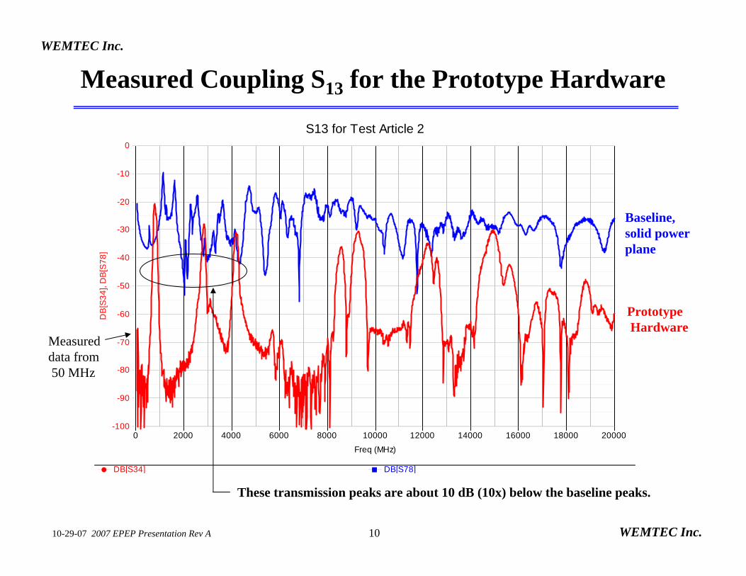
Measured Coupling S13 for the Prototype HardwareD
B[S
34],
DB
[S78
]
-100
-90
-80
-70
-60
-50
-40
-30
-20
-10
0
Freq (MHz)
0 2000 4000 6000 8000 10000 12000 14000 16000 18000 20000
S13 for Test Article 2
DB[S34] DB[S78]
These transmission peaks are about 10 dB (10x) below the baseline peaks.
PrototypeHardware
Measureddata from50 MHz
Baseline,solid powerplane
11
WEMTEC Inc.
WEMTEC Inc. 10-29-07 2007 EPEP Presentation Rev A
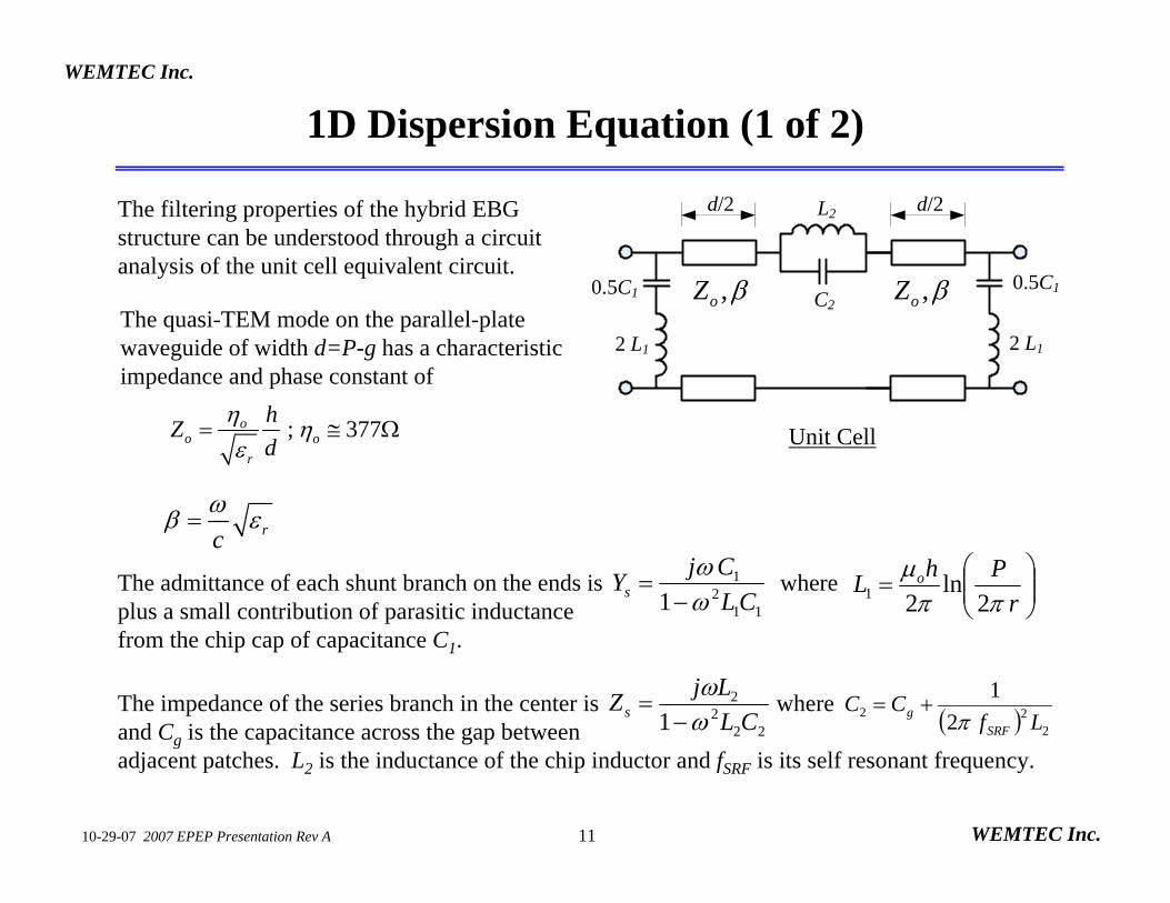
1D Dispersion Equation (1 of 2)
2 L1
0.5C1 C2
L2d/2 d/2
0.5C1
2 L1
,oZ β ,oZ β
The filtering properties of the hybrid EBG structure can be understood through a circuit analysis of the unit cell equivalent circuit.
The quasi-TEM mode on the parallel-plate waveguide of width d=P-g has a characteristic impedance and phase constant of
; 377oo o
r
hZd
η ηε
= ≅ Ω
rcωβ ε=
Unit Cell
The admittance of each shunt branch on the ends is whereplus a small contribution of parasitic inductance from the chip cap of capacitance C1.
112
1
1 CLCjYs ω
ω−
= ⎟⎟⎠
⎞⎜⎜⎝
⎛=
rPhL o
ππµ
2ln
21
The impedance of the series branch in the center is whereand Cg is the capacitance across the gap between adjacent patches. L2 is the inductance of the chip inductor and fSRF is its self resonant frequency.
222
2
1 CLLjZs ω
ω−
=( ) 2
22 21
LfCC
SRFg π+=

12
WEMTEC Inc.
WEMTEC Inc. 10-29-07 2007 EPEP Presentation Rev A
1D Dispersion Equation (2 of 2)
Calculate the ABCD parameters of the unit cell:
( )( )
( )( ) ⎥
⎥⎦
⎤
⎢⎢⎣
⎡⎥⎦
⎤⎢⎣
⎡⎥⎦
⎤⎢⎣
⎡⎥⎦
⎤⎢⎣
⎡
⎥⎥⎦
⎤
⎢⎢⎣
⎡=⎥
⎦
⎤⎢⎣
⎡1101
cos)sin()sin(cos
101
cos)sin()sin(cos
1101
so
os
o
o
s YlljYljZlZ
lljYljZl
YDCBA
ββββ
ββββ
where and . 2/dl = oo ZY /1=The propagation constant γx for Bloch waves that travel in the x (or y) direction along an infinite cascade of unit cells can be calculated from the ABCD parameters of one unit cell using the relation:
11 cosh .2x x x
A DjP
γ α β − += + =
( ) ( ) ( ) ( )cosh cos 1 cos sin4 2
s s o s o sx
Y Z Y Z Z YP d d j dγ β β β+⎡ ⎤= + + +⎡ ⎤⎣ ⎦ ⎢ ⎥⎣ ⎦
Since the unit cell network is symmetric, then A=D. After a few algebraic steps the dispersion equation for the Bloch wave propagation constant, γx, becomes
The attenuation constant αx defines the decay rate across a unit cell in nepers/meter as .The attenuation per unit cell can be calculated in dB using the following relationship:
xPe α−
[ ]20log exp( ) ( / )xAtten P dB unit cellα= −
13
WEMTEC Inc.
WEMTEC Inc. 10-29-07 2007 EPEP Presentation Rev A
0 2 4 6 8 100
10
20
30
40
50
Frequency (GHz)
Atte
n pe
r Uni
t Cel
l (dB
)
Atten2 f( )
Atten1 f( )
f
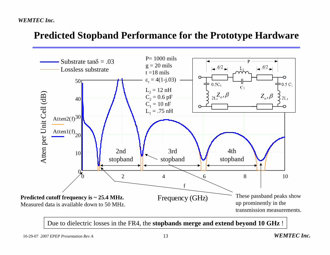
Predicted Stopband Performance for the Prototype Hardware
L2 = 12 nHC2 = 0.6 pFC1 = 10 nFL1 = .75 nH
P= 1000 milsg = 20 milst =18 milsεr = 4(1-j.03)
Predicted cutoff frequency is ~ 25.4 MHz.Measured data is available down to 50 MHz.
These passband peaks show up prominently in the transmission measurements.
,oZ β ,oZ β
Due to dielectric losses in the FR4, the stopbands merge and extend beyond 10 GHz !
Substrate tanδ = .03Lossless substrate
2ndstopband
3rdstopband
4thstopband
14
WEMTEC Inc.
WEMTEC Inc. 10-29-07 2007 EPEP Presentation Rev A
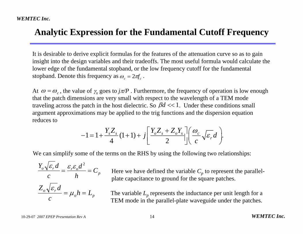
Analytic Expression for the Fundamental Cutoff Frequency
It is desirable to derive explicit formulas for the features of the attenuation curve so as to gain insight into the design variables and their tradeoffs. The most useful formula would calculate the lower edge of the fundamental stopband, or the low frequency cutoff for the fundamental stopband. Denote this frequency as .
At , the value of γx goes to jπ/P . Furthermore, the frequency of operation is low enough that the patch dimensions are very small with respect to the wavelength of a TEM mode traveling across the patch in the host dielectric. So . Under these conditions small argument approximations may be applied to the trig functions and the dispersion equation reduces to
cc fπω 2=
cωω =
1<<dβ
1 1 (1 1) .4 2
s s o s o s cr
Y Z Y Z Z Yj dcω ε+⎡ ⎤ ⎛ ⎞− = + + + ⎜ ⎟⎢ ⎥⎣ ⎦ ⎝ ⎠
We can simplify some of the terms on the RHS by using the following two relationships:
porro Ch
dc
dY==
2εεε
poro Lh
cdZ
== µε
Here we have defined the variable Cp to represent the parallel-plate capacitance to ground for the square patches.
The variable Lp represents the inductance per unit length for a TEM mode in the parallel-plate waveguide under the patches.
15
WEMTEC Inc.
WEMTEC Inc. 10-29-07 2007 EPEP Presentation Rev A
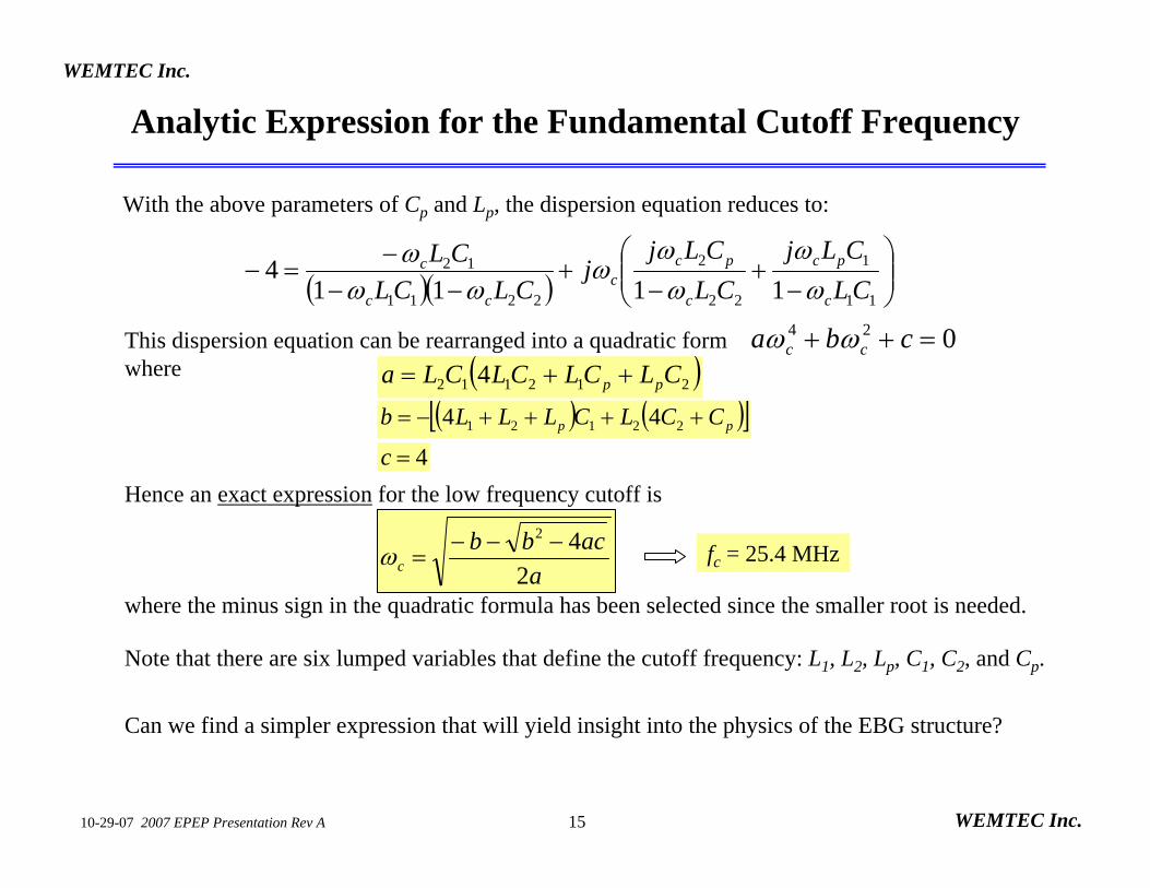
Analytic Expression for the Fundamental Cutoff Frequency
( )( ) ⎟⎟⎠
⎞⎜⎜⎝
⎛−
+−
+−−
−=−
11
1
22
2
2211
12
11114
CLCLj
CLCLj
jCLCL
CL
c
pc
c
pcc
cc
c
ωω
ωω
ωωω
ω
With the above parameters of Cp and Lp, the dispersion equation reduces to:
This dispersion equation can be rearranged into a quadratic formwhere
024 =++ cba cc ωω( )212112 4 CLCLCLCLa pp ++=
( ) ( )[ ]pp CCLCLLLb ++++−= 22121 44
4=cHence an exact expression for the low frequency cutoff is
aacbb
c 242 −−−
=ω
where the minus sign in the quadratic formula has been selected since the smaller root is needed.
Note that there are six lumped variables that define the cutoff frequency: L1, L2, Lp, C1, C2, and Cp.
Can we find a simpler expression that will yield insight into the physics of the EBG structure?
fc = 25.4 MHz
16
WEMTEC Inc.
WEMTEC Inc. 10-29-07 2007 EPEP Presentation Rev A
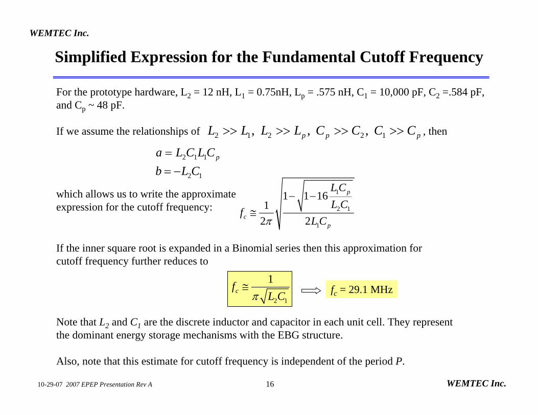
Simplified Expression for the Fundamental Cutoff Frequency
For the prototype hardware, L2 = 12 nH, L1 = 0.75nH, Lp = .575 nH, C1 = 10,000 pF, C2 =.584 pF, and Cp ~ 48 pF.
If we assume the relationships of , thenppp CCCCLLLL >>>>>>>> 12212 ,,,
pCLCLa 112=
12CLb −=
1
2 1
1
1 1 161
2 2
p
cp
L CL C
fL Cπ
− −≅
which allows us to write the approximate expression for the cutoff frequency:
If the inner square root is expanded in a Binomial series then this approximation for cutoff frequency further reduces to
2 1
1cf L Cπ≅
Note that L2 and C1 are the discrete inductor and capacitor in each unit cell. They represent the dominant energy storage mechanisms with the EBG structure.
Also, note that this estimate for cutoff frequency is independent of the period P.
fc = 29.1 MHz
17
WEMTEC Inc.
WEMTEC Inc. 10-29-07 2007 EPEP Presentation Rev A
1 .10 3 0.01 0.1 1 100
10
20
30
40
50
Frequency (GHz)
Atte
n pe
r Uni
t Cel
l (dB
)
Atten2 ff n( )Atten1 ff n( )
ff n
1 .10 3 0.01 0.1 1 100
10
20
30
40
50
Frequency (GHz)
Atte
n pe
r Uni
t Cel
l (dB
)
Atten2 ff n( )Atten1 ff n( )
ff n
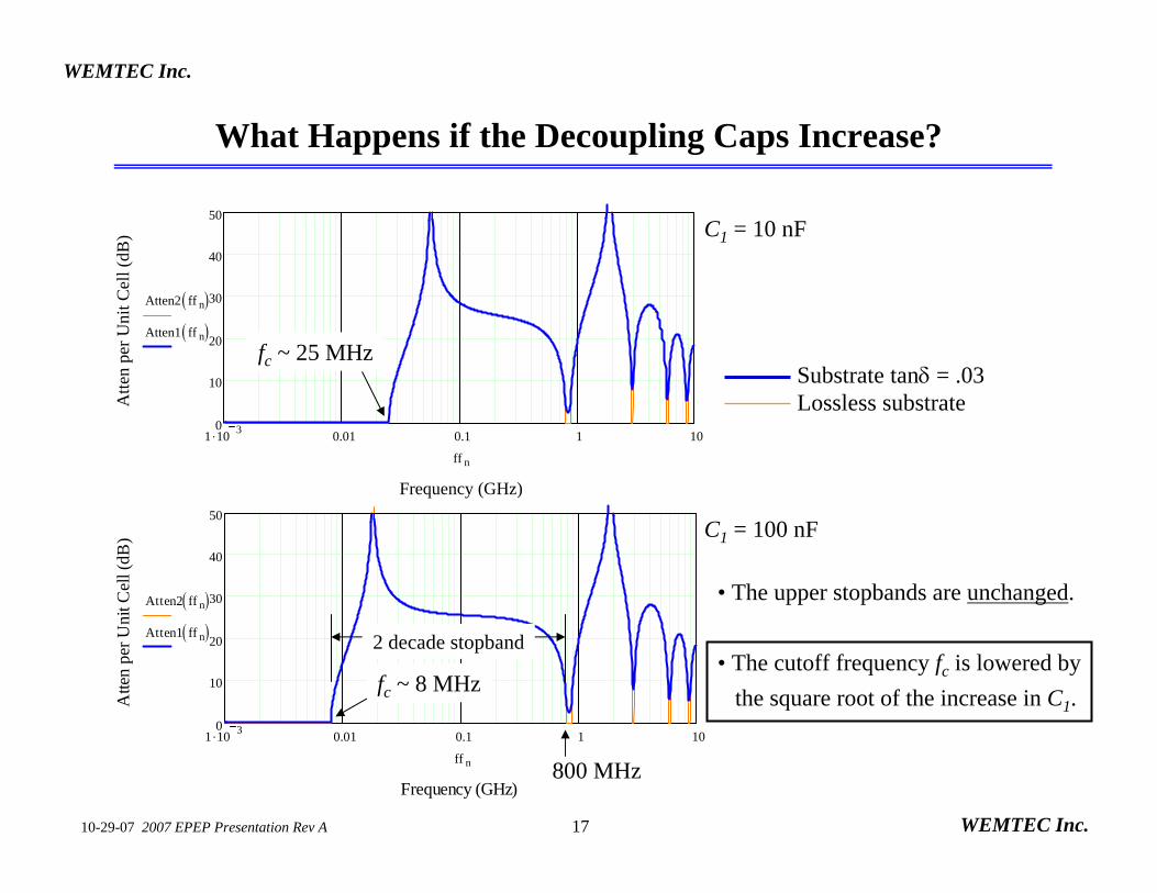
What Happens if the Decoupling Caps Increase?
C1 = 10 nF
C1 = 100 nF
• The upper stopbands are unchanged.
• The cutoff frequency fc is lowered bythe square root of the increase in C1.
Substrate tanδ = .03Lossless substrate
fc ~ 25 MHz
fc ~ 8 MHz
2 decade stopband
800 MHz
18
WEMTEC Inc.
WEMTEC Inc. 10-29-07 2007 EPEP Presentation Rev A
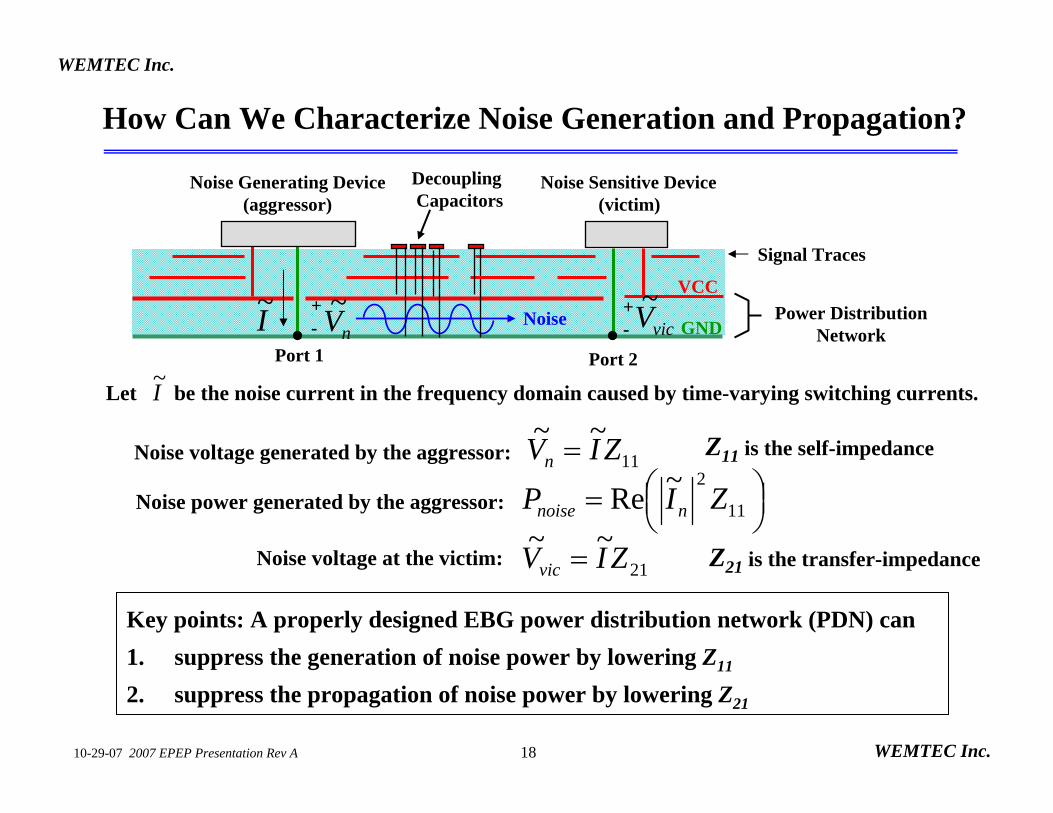
How Can We Characterize Noise Generation and Propagation?
Noise
Noise Sensitive Device(victim)
Signal Traces
Power DistributionNetwork
VCC
GND
DecouplingCapacitors
Noise Generating Device(aggressor)
11~~ ZIVn =
I~ +- nV~ vicV~+
-
Let be the noise current in the frequency domain caused by time-varying switching currents. I~
Noise voltage generated by the aggressor:
⎟⎠⎞⎜
⎝⎛= 11
2~Re ZIP nnoiseNoise power generated by the aggressor:
Noise voltage at the victim: 21~~ ZIVvic =
Key points: A properly designed EBG power distribution network (PDN) can 1. suppress the generation of noise power by lowering Z11
2. suppress the propagation of noise power by lowering Z21
Z11 is the self-impedance
Z21 is the transfer-impedance
Port 1 Port 2

19
WEMTEC Inc.
WEMTEC Inc. 10-29-07 2007 EPEP Presentation Rev A
10 100 1 .103 1 .10410 3
0.01
0.1
1
10
100
freqn
Measured Transfer Impedance Z12
50oZ = Ω1212
2o
SZ Z=∆
Measured data covers 50 MHz to 10 GHz
Fundamental Stopband
|Z12| (Ω)
(MHz)
2nd
Stopband
Improvement
Port 1Port 2
Prototype EBG Power Plane
Baseline,solid power plane
Dramatic improvements in transfer impedance are demonstrated for frequencies in the stopbands of the EBG power plane.
Noise limited
where 11 22 12 21(1 )(1 )S S S S∆ = − − − andNote:
20
WEMTEC Inc.
WEMTEC Inc. 10-29-07 2007 EPEP Presentation Rev A
Conclusions
• A new type of EBG structure is introduced for power distribution networks (PDNs)
• It combines the features of a periodic array of patches with- discrete (SMT) inductors as series elements, plus - discrete (SMT) decoupling capacitors within the patches.
• This EBG structure may be realized in microstrip or stripline construction.
•Stopband performance of the PDN up to at least several GHz may easily be predicted using a simple dispersion equation.
• The fundamental stopband has been demonstrated to start as low as 50 MHz with a prediction of 25 MHz.
• A fundamental stopband bandwidth ratio of greater than 30:1 is demonstrated.Ratios of 100:1 may be realized by increasing C1.
• The cutoff frequency fc for the fundamental stopband may be tailored throughcomponent selection for different areas of the PDN.
21
WEMTEC Inc.
WEMTEC Inc. 10-29-07 2007 EPEP Presentation Rev A
To Learn More
References on hybrid EBG structures:
[1] Will McKinzie, “A Low Frequency Hybrid EBG Structure for Power Plane Noise Suppression,” IEEE 15th Topical Meeting on Electrical Performance of Electronic Packaging, Oct 23-25, 2006, Scottsdale, AZ, pp. 51-54.
[2] William E. McKinzie III, “Systems and Methods for Electromagnetic Noise Suppression Using Hybrid Electromagnetic Bandgap Structures,” US Patent Publication 2007/0090398, published April 26, 2007.
References on inductive grid EBG structures using discrete inductors:
[3] Ki Hyuk Kim et. al., “Design of EBG Power Distribution Networks with VHF-Band Cutoff Frequency and Small Unit Cell Size for Mixed-Signal Systems,” IEEE Microwave and Wireless Components Letters, Vol. 17, No. 7, July 2007, pp.489-491.
22
WEMTEC Inc.
WEMTEC Inc. 10-29-07 2007 EPEP Presentation Rev A
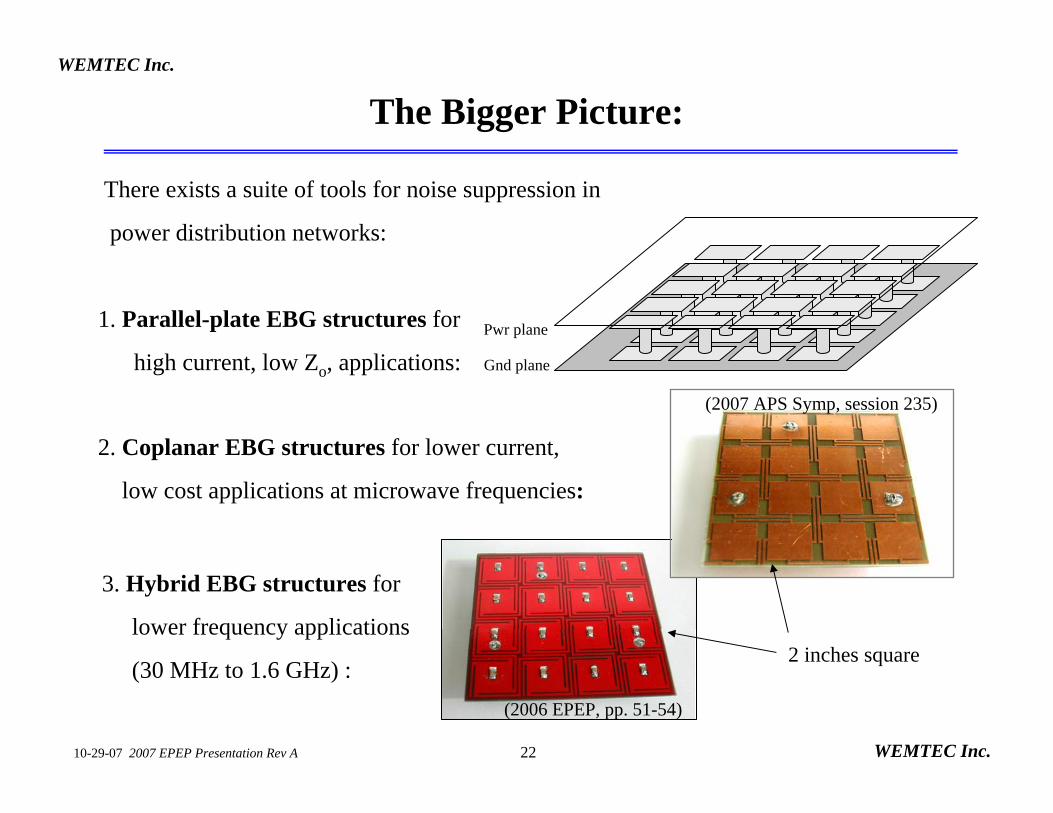
The Bigger Picture:
There exists a suite of tools for noise suppression in
power distribution networks:
1. Parallel-plate EBG structures for
high current, low Zo, applications:Pwr plane
Gnd plane
(2006 EPEP, pp. 51-54)
(2007 APS Symp, session 235)
2. Coplanar EBG structures for lower current,
low cost applications at microwave frequencies:
3. Hybrid EBG structures for
lower frequency applications
(30 MHz to 1.6 GHz) :2 inches square