a logarithmic detector/controller 0.1 ghz–2.5 ghz, 70 … sheets/analog devices... ·...
TRANSCRIPT

REV. C
aAD8313
Information furnished by Analog Devices is believed to be accurate andreliable. However, no responsibility is assumed by Analog Devices for itsuse, nor for any infringements of patents or other rights of third parties thatmay result from its use. No license is granted by implication or otherwiseunder any patent or patent rights of Analog Devices. Trademarks andregistered trademarks are the property of their respective companies.
One Technology Way, P.O. Box 9106, Norwood, MA 02062-9106, U.S.A.
Tel: 781/329-4700 www.analog.com
Fax: 781/326-8703 © 2003 Analog Devices, Inc. All rights reserved.
0.1 GHz–2.5 GHz, 70 dBLogarithmic Detector/Controller
FUNCTIONAL BLOCK DIAGRAM
+ + ++ +
AD8313
VOUT
VSET
COMM
PWDNGAINBIAS
BAND-GAPREFERENCE
SLOPECONTROL
INTERCEPTCONTROL
EIGHT 8dB 3.5GHz AMPLIFIER STAGES
8dB 8dB
VPOS
INHI
INLO
VPOS
8dB8dB
NINE DETECTOR CELLS
CINT
LP
IvV
VvI
GENERAL DESCRIPTIONThe AD8313 is a complete multistage demodulating logarithmicamplifier, capable of accurately converting an RF signal at itsdifferential input to an equivalent decibel-scaled value at itsdc output. The AD8313 maintains a high degree of log conform-ance for signal frequencies from 0.1 GHz to 2.5 GHz and is usefulover the range of 10 MHz to 3.5 GHz. The nominal inputdynamic range is –65 dBm to 0 dBm (re: 50 W), and the sensi-tivity can be increased by 6 dB or more with a narrow-band inputimpedance matching network or balun. Application is straight-forward, requiring only a single supply of 2.7 V to 5.5 V and theaddition of a suitable input and supply decoupling. Operating ona 3 V supply, its 13.7 mA consumption (for TA = 25∞C) amountsto only 41 mW. A power-down feature is provided; the input istaken high to initiate a low current (20 mA) sleep mode, with athreshold at half the supply voltage.
The AD8313 uses a cascade of eight amplifier/limiter cells, eachhaving a nominal gain of 8 dB and a –3 dB bandwidth of 3.5 GHz,for a total midband gain of 64 dB. At each amplifier output,a detector (rectifier) cell is used to convert the RF signal to base-band form; a ninth detector cell is placed directly at the input ofthe AD8313. The current-mode outputs of these cells are summedto generate a piecewise linear approximation to the logarithmicfunction, and converted to a low impedance voltage-mode outputby a transresistance stage, which also acts as a low-pass filter.
When used as a log amp, the scaling is determined by a separatefeedback interface (a transconductance stage) that sets the slope
to approximately 18 mV/dB; used as a controller, this stage acceptsthe setpoint input. The logarithmic intercept is positioned tonearly –100 dBm, and the output runs from about 0.45 V dcat –73 dBm input to 1.75 V dc at 0 dBm input. The scale andintercept are supply and temperature stable.
The AD8313 is fabricated on Analog Devices’ advanced 25 GHzsilicon bipolar IC process and is available in an 8-lead MSOPpackage. The operating temperature range is –40∞C to +85∞C.An evaluation board is available.
INPUT AMPLITUDE – dBm
2.0
–80
OU
TP
UT
VO
LT
AG
E –
V D
C
1.8
1.6
1.4
1.2
1.0
0.8
0.6
0.4
0.2
0–70 –60 –50 –40 –30 –20 –10 0
FREQUENCY = 1.9GHz5
4
3
2
1
0
–1
–2
–3
–4
–5
OU
TP
UT
ER
RO
R –
dB
Figure 1. Typical Logarithmic Response and Errorvs. Input Amplitude
FEATURES
Wide Bandwidth: 0.1 GHz to 2.5 GHz Min
High Dynamic Range: 70 dB to 63.0 dB
High Accuracy: 61.0 dB over 65 dB Range (@ 1.9 GHz)
Fast Response: 40 ns Full-Scale Typical
Controller Mode with Error Output
Scaling Stable Over Supply and Temperature
Wide Supply Range: 2.7 V to 5.5 V
Low Power: 40 mW at 3 V
Power-Down Feature: 60 mW at 3 V
Complete and Easy to Use
APPLICATIONS
RF Transmitter Power Amplifier Setpoint Control and
Level Monitoring
Logarithmic Amplifier for RSSI Measurement Cellular
Base Stations, Radio Link, Radar

–2– REV. C
AD8313–SPECIFICATIONS (@ TA = 25�C, VS = 5 V1, RL ≥ 10 k�, unless otherwise noted.)
Parameter Conditions Min2 Typ Max2 Unit
SIGNAL INPUT INTERFACESpecified Frequency Range 0.1 2.5 GHzDC Common-Mode Voltage VPOS – 0.75 VInput Bias Currents 10 mAInput Impedance fRF < 100 MHz3 900�1.1 W�pF4
LOG (RSSI) MODE Sinusoidal, input termination configuration shown in Figure 11.100 MHz5 Nominal Conditions
± 3 dB Dynamic Range6 53.5 65 dBRange Center –31.5 dBm
± 1 dB Dynamic Range 56 dBSlope 17 19 21 mV/dBIntercept –96 –88 –80 dBm
2.7 V £ VS £ 5.5 V, –40∞C £ T £ +85∞C± 3 dB Dynamic Range 51 64 dB
Range Center –31 dBm± 1 dB Dynamic Range 55 dBSlope 16 19 22 mV/dBIntercept –99 –89 –75 dBmTemperature Sensitivity PIN = –10 dBm –0.022 dB/∞C
900 MHz5 Nominal Conditions± 3 dB Dynamic Range 60 69 dB
Range Center –32.5 dBm± 1 dB Dynamic Range 62 dBSlope 15.5 18 20.5 mV/dBIntercept –105 –93 –81 dBm
2.7 V £ VS £ 5.5 V, –40∞C £ T £ +85∞C± 3 dB Dynamic Range 55.5 68.5 dB
Range Center –32.75 dBm± 1 dB Dynamic Range 61 dBSlope 15 18 21 mV/dBIntercept –110 –95 –80 dBmTemperature Sensitivity PIN = –10 dBm –0.019 dB/∞C
1.9 GHz7 Nominal Conditions± 3 dB Dynamic Range 52 73 dB
Range Center –36.5 dBm± 1 dB Dynamic Range 62 dBSlope 15 17.5 20.5 mV/dBIntercept –115 –100 –85 dBm
2.7 V £ VS £ 5.5 V, –40∞C £ T £ +85∞C± 3 dB Dynamic Range 50 73 dB
Range Center –36.5 dBm± 1 dB Dynamic Range 60 dBSlope 14 17.5 21.5 mV/dBIntercept –125 –101 –78 dBmTemperature Sensitivity PIN = –10 dBm –0.019 dB/∞C
2.5 GHz7 Nominal Conditions± 3 dB Dynamic Range 48 66 dB
Range Center –34 dBm± 1 dB Dynamic Range 46 dBSlope 16 20 25 mV/dBIntercept –111 –92 –72 dBm
2.7 V £ VS £ +5.5 V, –40∞C £ T £ 85∞C± 3 dB Dynamic Range 47 68 dB
Range Center –34.5 dBm± 1 dB Dynamic Range 46 dBSlope 14.5 20 25 mV/dBIntercept –128 –92 –56 dBmTemperature Sensitivity PIN = –10 dBm –0.040 dB/∞C

–3–REV. C
AD8313Parameter Conditions Min2 Typ Max2 Unit
3.5 GHz5 Nominal Conditions± 3 dB Dynamic Range 43 dB± 1 dB Dynamic Range 35 dBSlope 24 mV/dBIntercept –65 dBm
CONTROL MODEController Sensitivity f = 900 MHz 23 V/dBLow Frequency Gain VSET to VOUT8 84 dBOpen-Loop Corner Frequency VSET to VOUT8 700 HzOpen-Loop Slew Rate f = 900 MHz 2.5 V/msVSET Delay Time 150 ns
VOUT INTERFACECurrent Drive Capability
Source Current 400 mA
Sink Current 10 mA
Minimum Output Voltage Open-Loop 50 mVMaximum Output Voltage Open-Loop VPOS – 0.1 VOutput Noise Spectral Density PIN = –60 dBm, fSPOT = 100 Hz 2.0 mV/÷Hz
PIN = –60 dBm, fSPOT = 10 MHz 1.3 mV/÷HzSmall Signal Response Time PIN = –60 dBm to –57 dBm, 10% to 90% 40 60 nsLarge Signal Response Time PIN = No Signal to 0 dBm, Settled to 0.5 dB 110 160 ns
VSET INTERFACEInput Voltage Range 0 VPOS VInput Impedance 18�1 kW�pF4
POWER-DOWN INTERFACEPWDN Threshold VPOS/2 VPower-Up Response Time Time delay following high to low transition
until device meets full specifications. 1.8 msPWDN Input Bias Current PWDN = 0 V 5 mA
PWDN = VS <1 mA
POWER SUPPLYOperating Range 2.7 5.5 VPowered-Up Current 13.7 15.5 mA
4.5 V £ VS £ 5.5 V, –40∞C £ T £ +85∞C 18.5 mA2.7 V £ VS £ 3.3 V, –40∞C £ T £ +85∞C 18.5 mA
Powered-Down Current 4.5 V £ VS £ 5.5 V, –40∞C £ T £ +85∞C 50 150 mA2.7 V £ VS £ 3.3 V, –40∞C £ T £ +85∞C 20 50 mA
NOTES1Except where otherwise noted, performance at VS = 3 V is equivalent to 5 V operation.2Minimum and maximum specified limits on parameters that are guaranteed but not tested are six sigma values.3Input impedance shown over frequency range in Figure 8.4Double vertical bars (�) denote “in parallel with.”5Linear regression calculation for error curve taken from –40 dBm to –10 dBm for all parameters.6Dynamic range refers to range over which the linearity error remains within the stated bound.7Linear regression calculation for error curve taken from –60 dBm to –5 dBm for 3 dB dynamic range. All other regressions taken from –40 dBm to –10 dBm.8AC response shown in TPC 9.
Specifications subject to change without notice.
AD8313
–4– REV. C
CAUTIONESD (electrostatic discharge) sensitive device. Electrostatic charges as high as 4000 V readilyaccumulate on the human body and test equipment and can discharge without detection. Althoughthe AD8313 features proprietary ESD protection circuitry, permanent damage may occur ondevices subjected to high energy electrostatic discharges. Therefore, proper ESD precautions arerecommended to avoid performance degradation or loss of functionality.
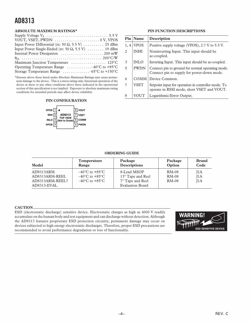
ABSOLUTE MAXIMUM RATINGS*
Supply Voltage VS . . . . . . . . . . . . . . . . . . . . . . . . . . . . . . 5.5 VVOUT, VSET, PWDN . . . . . . . . . . . . . . . . . . . . . . 0 V, VPOSInput Power Differential (re: 50 W, 5.5 V) . . . . . . . . . . 25 dBmInput Power Single-Ended (re: 50 W, 5.5 V) . . . . . . . . 19 dBmInternal Power Dissipation . . . . . . . . . . . . . . . . . . . . . 200 mWqJA . . . . . . . . . . . . . . . . . . . . . . . . . . . . . . . . . . . . . . . 200∞C/WMaximum Junction Temperature . . . . . . . . . . . . . . . . . 125∞COperating Temperature Range . . . . . . . . . . . . –40∞C to +85∞CStorage Temperature Range . . . . . . . . . . . . . –65∞C to +150∞C*Stresses above those listed under Absolute Maximum Ratings may cause perma-
nent damage to the device. This is a stress rating only; functional operation of thedevice at these or any other conditions above those indicated in the operationalsection of this specification is not implied. Exposure to absolute maximum ratingconditions for extended periods may affect device reliability.
PIN CONFIGURATION
TOP VIEW(Not to Scale)
8
7
6
5
1
2
3
4
VPOS
INHI
INLO
VPOS
VOUT
VSET
COMM
PWDN
AD8313
ORDERING GUIDE
Temperature Package Package BrandModel Range Descriptions Option Code
AD8313ARM –40∞C to +85∞C 8-Lead MSOP RM-08 J1AAD8313ARM-REEL –40∞C to +85∞C 13" Tape and Reel RM-08 J1AAD8313ARM-REEL7 –40∞C to +85∞C 7" Tape and Reel RM-08 J1AAD8313-EVAL Evaluation Board
PIN FUNCTION DESCRIPTIONS
Pin Name Description
1, 4 VPOS Positive supply voltage (VPOS), 2.7 V to 5.5 V.
2 INHI Noninverting Input. This input should beac-coupled.
3 INLO Inverting Input. This input should be ac-coupled.
5 PWDN Connect pin to ground for normal operating mode.Connect pin to supply for power-down mode.
6 COMM Device Common.
7 VSET Setpoint input for operation in controller mode. Tooperate in RSSI mode, short VSET and VOUT.
8 VOUT Logarithmic/Error Output.

AD8313
–5–REV. C
INPUT AMPLITUDE – dBm
2.0
–70
VO
UT –
V1.8
1.6
1.4
1.2
1.0
0.8
0.6
0.4
0.2
0–60 –50 –40 –30 –20 –10 0 10
VS = +5VINPUT MATCH SHOWN IN FIGURE 11
1.9GHz 2.5GHz
900MHz
100MHz
TPC 1. VOUT vs. Input Amplitude
INPUT AMPLITUDE – dBm
6
–6–70 10–60
ER
RO
R –
dB
–50 –40 –30 –20 –10 0
4
2
0
–2
–4
900MHz
100MHz
100MHz
900MHz
1.9GHz2.5GHz
2.5GHz
1.9GHz
VS = +5VINPUT MATCH SHOWN IN FIGURE 11
TPC 2. Log Conformance vs. Input Amplitude
INPUT AMPLITUDE – dBm
2.0
–70
VO
UT –
V
1.8
1.6
1.4
1.2
1.0
0.8
0.6
0.4
0.2
0–60 –50 –40 –30 –20 –10 0 10
VS = +5VINPUT MATCH SHOWN IN FIGURE 11
5
4
3
2
1
0
–1
–2
–3
–4
–5
ER
RO
R –
dB–40�C
+25�C
+85�C
SLOPE AND INTERCEPT NORMALIZED AT +25�CAND APPLIED TO –40�C AND +85�C
TPC 3. VOUT and Log Conformance vs. InputAmplitude at 100 MHz; –40∞C, +25∞C, and +85∞C
Typical Performance Characteristics–
INPUT AMPLITUDE – dBm
2.0
–70
VO
UT –
V
1.8
1.6
1.4
1.2
1.0
0.8
0.6
0.4
0.2
0–60 –50 –40 –30 –20 –10 0 10
VS = +5VINPUT MATCH SHOWN IN FIGURE 11
5
4
3
2
1
0
–1
–2
–3
–4
–5
ER
RO
R –
dB
+25�C
+85�C
–40�C
SLOPE AND INTERCEPT NORMALIZED AT +25�CAND APPLIED TO –40�C AND +85�C
TPC 4. VOUT and Log Conformance vs. InputAmplitude at 900 MHz; –40∞C, +25∞C, and +85∞C
INPUT AMPLITUDE – dBm
2.0
–70
VO
UT –
V
1.8
1.6
1.4
1.2
1.0
0.8
0.6
0.4
0.2
0–60 –50 –40 –30 –20 –10 0 10
VS = +5VINPUT MATCH SHOWN IN FIGURE 11
5
4
3
2
1
0
–1
–2
–3
–4
–5
ER
RO
R –
dB
–40�C
+25�C
+85�C
SLOPE AND INTERCEPT NORMALIZED AT +25�CAND APPLIED TO –40�C AND +85�C
TPC 5. VOUT and Log Conformance vs. InputAmplitude at 1.9 GHz; –40∞C, +25∞C, and +85∞C
INPUT AMPLITUDE – dBm
2.0
–70
VO
UT –
V
1.8
1.6
1.4
1.2
1.0
0.8
0.6
0.4
0.2
0–60 –50 –40 –30 –20 –10 0 10
VS = +5VINPUT MATCH SHOWN IN FIGURE 11
5
4
3
2
1
0
–1
–2
–3
–4
–5
ER
RO
R –
dB
–40�C
+25�C
+85�C
SLOPE AND INTERCEPTNORMALIZED AT +25�C ANDAPPLIED TO –40�C AND +85�C
TPC 6. VOUT and Log Conformance vs. InputAmplitude at 2.5 GHz; –40∞C, +25∞C, and +85∞C
AD8313
–6– REV. C
FREQUENCY – MHz
22
21
160 2500500
SL
OP
E –
mV
/dB
1000 1500 2000
20
19
18
17
VPS = +5VINPUT MATCH SHOWN IN FIGURE 11
–40�C
+25�C
+85�C
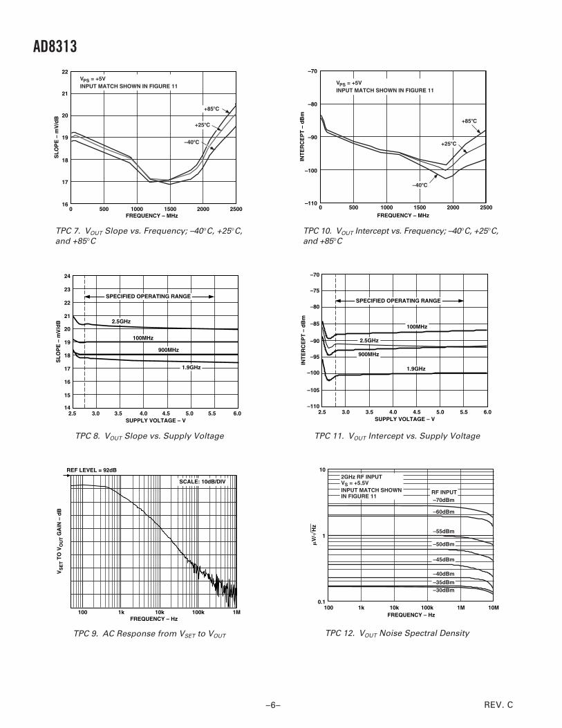
TPC 7. VOUT Slope vs. Frequency; –40∞C, +25∞C,and +85∞C
SUPPLY VOLTAGE – V
24
2.5
SL
OP
E –
mV
/dB
23
22
21
20
19
18
17
16
15
143.0 3.5 4.0 4.5 5.0 5.5 6.0
1.9GHz
2.5GHz
900MHz
100MHz
SPECIFIED OPERATING RANGE
TPC 8. VOUT Slope vs. Supply Voltage
FREQUENCY – Hz
VS
ET T
O V
OU
T G
AIN
– d
B
100 1k 10k 100k 1M
REF LEVEL = 92dB
SCALE: 10dB/DIV
TPC 9. AC Response from VSET to VOUT
FREQUENCY – MHz
–1100 2500500
INT
ER
CE
PT
– d
Bm
1000 1500 2000
–70
–80
–90
–100
+85�C
–40�C
+25�C
VPS = +5VINPUT MATCH SHOWN IN FIGURE 11
TPC 10. VOUT Intercept vs. Frequency; –40∞C, +25∞C,and +85∞C
SUPPLY VOLTAGE – V
–70
2.5
INT
ER
CE
PT
– d
Bm
–75
–80
–85
–90
–95
–100
–105
–1103.0 3.5 4.0 4.5 5.0 5.5 6.0
1.9GHz
2.5GHz
900MHz
100MHz
SPECIFIED OPERATING RANGE
TPC 11. VOUT Intercept vs. Supply Voltage
FREQUENCY – Hz100
10
0.1
�V
/ H
z
1
1k 10k 100k 1M 10M
2GHz RF INPUTVS = +5.5VINPUT MATCH SHOWNIN FIGURE 11
RF INPUT–70dBm
–60dBm
–55dBm
–50dBm
–45dBm
–40dBm
–35dBm–30dBm
TPC 12. VOUT Noise Spectral Density
AD8313
–7–REV. C
PWDN VOLTAGE – V0
100.00S
UP
PL
Y C
UR
RE
NT
– m
A 10.00
1.00
0.10
0.011 2 3 4 5
40�A
VPOS = +5VVPOS = +3V
20�A
13.7mA
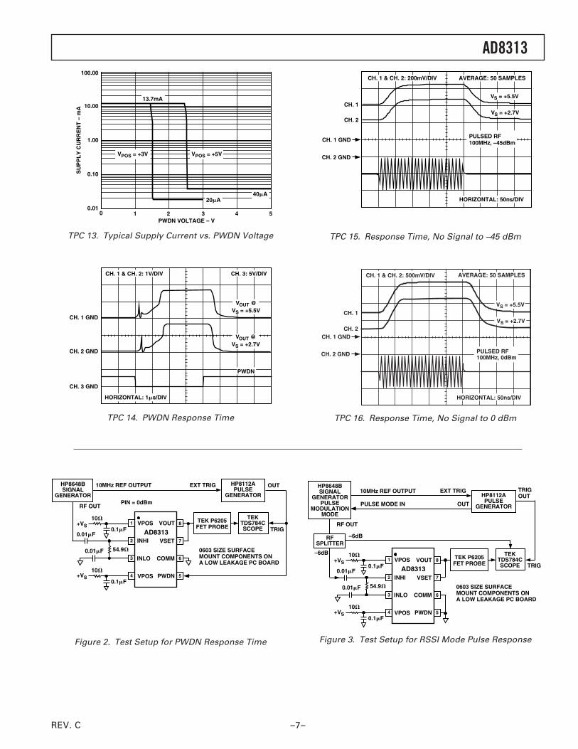
TPC 13. Typical Supply Current vs. PWDN Voltage
CH. 1 & CH. 2: 1V/DIV CH. 3: 5V/DIV
HORIZONTAL: 1�s/DIV
VOUT @VS = +5.5V
VOUT @VS = +2.7V
PWDN
CH. 1 GND
CH. 2 GND
CH. 3 GND
TPC 14. PWDN Response Time
0.1�F
54.9�0.01�F
0.01�F
10�
10�
0.1�F
+VS
+VS
TEKTDS784CSCOPE
8
7
6
5
1
2
3
4
VPOS VOUT
INHI
INLO
VPOS PWDN
COMM
VSETAD8313
TEK P6205FET PROBE TRIG
0603 SIZE SURFACEMOUNT COMPONENTS ONA LOW LEAKAGE PC BOARD
EXT TRIG OUTHP8112APULSE
GENERATORPIN = 0dBm
RF OUT
HP8648BSIGNAL
GENERATOR
10MHz REF OUTPUT
Figure 2. Test Setup for PWDN Response Time
CH. 1
CH. 1 GND
CH. 2 GND
CH. 2
CH. 1 & CH. 2: 200mV/DIV AVERAGE: 50 SAMPLES
VS = +5.5V
VS = +2.7V
HORIZONTAL: 50ns/DIV
PULSED RF100MHz, –45dBm
TPC 15. Response Time, No Signal to –45 dBm
CH. 1 & CH. 2: 500mV/DIV AVERAGE: 50 SAMPLES
HORIZONTAL: 50ns/DIV
CH. 1 GND
CH. 2 GND PULSED RF100MHz, 0dBm
CH. 1
CH. 2
VS = +5.5V
VS = +2.7V
TPC 16. Response Time, No Signal to 0 dBm
0.1�F
54.9�0.01�F
0.01�F
10�
10�
0.1�F
+VS
+VS
TEKTDS784CSCOPE
8
7
6
5
1
2
3
4
VPOS VOUT
INHI
INLO
VPOS PWDN
COMM
VSET
AD8313
TEK P6205FET PROBE
TRIGOUT
0603 SIZE SURFACEMOUNT COMPONENTS ONA LOW LEAKAGE PC BOARD
EXT TRIGHP8112APULSE
GENERATOR
RF OUT
10MHz REF OUTPUT
–6dB
RFSPLITTER
–6dB
HP8648BSIGNAL
GENERATORPULSE
MODULATIONMODE
PULSE MODE IN OUT
TRIG
Figure 3. Test Setup for RSSI Mode Pulse Response
AD8313
–8– REV. C
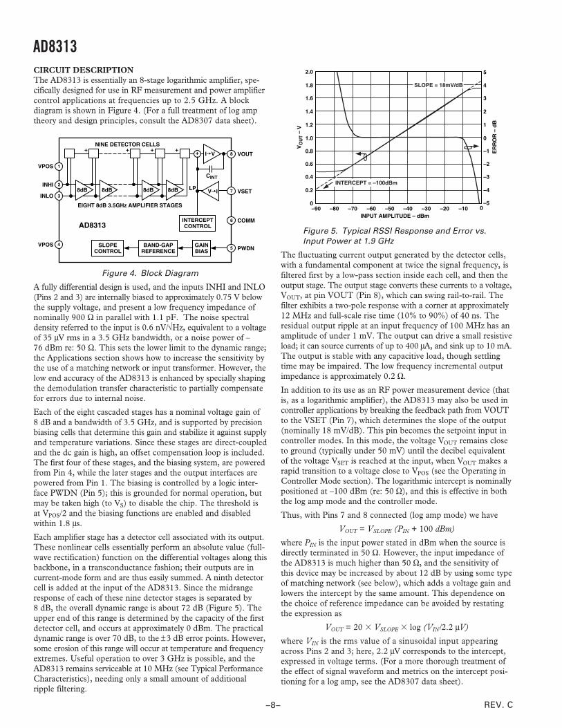
CIRCUIT DESCRIPTIONThe AD8313 is essentially an 8-stage logarithmic amplifier, spe-cifically designed for use in RF measurement and power amplifiercontrol applications at frequencies up to 2.5 GHz. A blockdiagram is shown in Figure 4. (For a full treatment of log amptheory and design principles, consult the AD8307 data sheet).
+ + ++ +
AD8313
VOUT
VSET
COMM
PWDNGAINBIAS
BAND-GAPREFERENCE
SLOPECONTROL
INTERCEPTCONTROL
EIGHT 8dB 3.5GHz AMPLIFIER STAGES
8dB 8dB
VPOS
INHI
INLO
VPOS
8dB8dB
NINE DETECTOR CELLS
CINT
LP
IvV
VvI
Figure 4. Block Diagram
A fully differential design is used, and the inputs INHI and INLO(Pins 2 and 3) are internally biased to approximately 0.75 V belowthe supply voltage, and present a low frequency impedance ofnominally 900 W in parallel with 1.1 pF. The noise spectraldensity referred to the input is 0.6 nV/÷Hz, equivalent to a voltageof 35 mV rms in a 3.5 GHz bandwidth, or a noise power of –76 dBm re: 50 W. This sets the lower limit to the dynamic range;the Applications section shows how to increase the sensitivity bythe use of a matching network or input transformer. However, thelow end accuracy of the AD8313 is enhanced by specially shapingthe demodulation transfer characteristic to partially compensatefor errors due to internal noise.
Each of the eight cascaded stages has a nominal voltage gain of8 dB and a bandwidth of 3.5 GHz, and is supported by precisionbiasing cells that determine this gain and stabilize it against supplyand temperature variations. Since these stages are direct-coupledand the dc gain is high, an offset compensation loop is included.The first four of these stages, and the biasing system, are poweredfrom Pin 4, while the later stages and the output interfaces arepowered from Pin 1. The biasing is controlled by a logic inter-face PWDN (Pin 5); this is grounded for normal operation, butmay be taken high (to VS) to disable the chip. The threshold isat VPOS/2 and the biasing functions are enabled and disabledwithin 1.8 ms.
Each amplifier stage has a detector cell associated with its output.These nonlinear cells essentially perform an absolute value (full-wave rectification) function on the differential voltages along thisbackbone, in a transconductance fashion; their outputs are incurrent-mode form and are thus easily summed. A ninth detectorcell is added at the input of the AD8313. Since the midrangeresponse of each of these nine detector stages is separated by8 dB, the overall dynamic range is about 72 dB (Figure 5). Theupper end of this range is determined by the capacity of the firstdetector cell, and occurs at approximately 0 dBm. The practicaldynamic range is over 70 dB, to the ± 3 dB error points. However,some erosion of this range will occur at temperature and frequencyextremes. Useful operation to over 3 GHz is possible, and theAD8313 remains serviceable at 10 MHz (see Typical PerformanceCharacteristics), needing only a small amount of additionalripple filtering.
INPUT AMPLITUDE – dBm
2.0
–80
VO
UT –
V
1.8
1.6
1.4
1.2
1.0
0.8
0.6
0.4
0.2
0–70 –60 –50 –40 –30 –20 –10 0
5
4
3
2
1
0
–1
–2
–3
–4
–5
ER
RO
R –
dB
–90
INTERCEPT = –100dBm
SLOPE = 18mV/dB
Figure 5. Typical RSSI Response and Error vs.Input Power at 1.9 GHz
The fluctuating current output generated by the detector cells,with a fundamental component at twice the signal frequency, isfiltered first by a low-pass section inside each cell, and then theoutput stage. The output stage converts these currents to a voltage,VOUT, at pin VOUT (Pin 8), which can swing rail-to-rail. Thefilter exhibits a two-pole response with a corner at approximately12 MHz and full-scale rise time (10% to 90%) of 40 ns. Theresidual output ripple at an input frequency of 100 MHz has anamplitude of under 1 mV. The output can drive a small resistiveload; it can source currents of up to 400 mA, and sink up to 10 mA.The output is stable with any capacitive load, though settlingtime may be impaired. The low frequency incremental outputimpedance is approximately 0.2 W.
In addition to its use as an RF power measurement device (thatis, as a logarithmic amplifier), the AD8313 may also be used incontroller applications by breaking the feedback path from VOUTto the VSET (Pin 7), which determines the slope of the output(nominally 18 mV/dB). This pin becomes the setpoint input incontroller modes. In this mode, the voltage VOUT remains closeto ground (typically under 50 mV) until the decibel equivalentof the voltage VSET is reached at the input, when VOUT makes arapid transition to a voltage close to VPOS (see the Operating inController Mode section). The logarithmic intercept is nominallypositioned at –100 dBm (re: 50 W), and this is effective in boththe log amp mode and the controller mode.
Thus, with Pins 7 and 8 connected (log amp mode) we have
VOUT = VSLOPE (PIN + 100 dBm)
where PIN is the input power stated in dBm when the source isdirectly terminated in 50 W. However, the input impedance ofthe AD8313 is much higher than 50 W, and the sensitivity ofthis device may be increased by about 12 dB by using some typeof matching network (see below), which adds a voltage gain andlowers the intercept by the same amount. This dependence onthe choice of reference impedance can be avoided by restatingthe expression as
VOUT = 20 � VSLOPE � log (VIN/2.2 mV)
where VIN is the rms value of a sinusoidal input appearingacross Pins 2 and 3; here, 2.2 mV corresponds to the intercept,expressed in voltage terms. (For a more thorough treatment ofthe effect of signal waveform and metrics on the intercept posi-tioning for a log amp, see the AD8307 data sheet).
AD8313
–9–REV. C
With Pins 7 and 8 disconnected (controller mode), the outputmay be stated as
VOUT v VS when VSLOPE (PIN + 100) > VSET
VOUT v 0 when VSLOPE (PIN + 100) < VSET
when the input is stated in terms of the power of a sinusoidalsignal across a net termination impedance of 50 W. The transi-tion zone between high and low states is very narrow, since theoutput stage behaves essentially as a fast integrator. The aboveequations may be restated as
VOUT v VS when VSLOPE log (VIN/2.2 mV) > VSET
VOUT v 0 when VSLOPE log (VIN/2.2 mV) < VSET
A further use of the separate VOUT and VSET pins is in raisingthe load-driving current capability by the inclusion of an externalNPN emitter follower. More complete information about usagein these various modes is provided in the Applications section.
INTERFACESThis section describes the signal and control interfaces and theirbehavior. On-chip resistances and capacitances exhibit variationsof up to ± 20%. These resistances are sometimes temperaturedependent and the capacitances may be voltage dependent.
Power-Down Interface, PWDNThe power-down threshold is accurately centered at the midpointof the supply as shown in Figure 6. If Pin 5 is left unconnected ortied to the supply voltage (recommended), the bias enable currentis shut off, and the current drawn from the supply is predominatelythrough a nominal 300 kW chain (20 mA at 3 V). When grounded,the bias system is turned on. The threshold level is accurately atVPOS/2. The input bias current at the PWDN pin when operatingin the device ON state is approximately 5 mA for VPOS = 3 V.
5PWDN
VPOS
75k�
6COMM
150k�50k�
150k�
TO BIASENABLE
4
Figure 6. Power-Down Threshold Circuitry
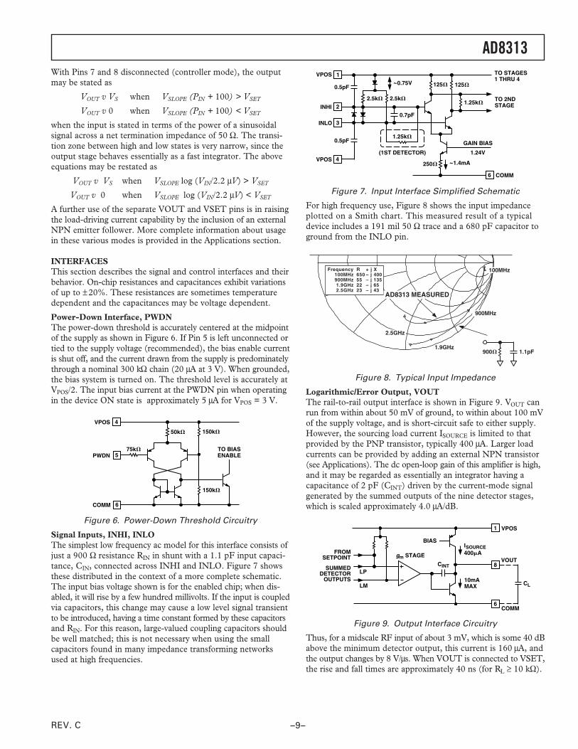
Signal Inputs, INHI, INLOThe simplest low frequency ac model for this interface consists ofjust a 900 W resistance RIN in shunt with a 1.1 pF input capaci-tance, CIN, connected across INHI and INLO. Figure 7 showsthese distributed in the context of a more complete schematic.The input bias voltage shown is for the enabled chip; when dis-abled, it will rise by a few hundred millivolts. If the input is coupledvia capacitors, this change may cause a low level signal transientto be introduced, having a time constant formed by these capacitorsand RIN. For this reason, large-valued coupling capacitors shouldbe well matched; this is not necessary when using the smallcapacitors found in many impedance transforming networksused at high frequencies.
1.25k�
COMM
VPOS
INHI
INLO
VPOS
0.5pF
0.5pF
0.7pF
2.5k� 2.5k�
~0.75V
(1ST DETECTOR)
250� ~1.4mA
125� 125�
1.25k�
1.24V
GAIN BIAS
TO 2NDSTAGE
TO STAGES1 THRU 4
1
2
3
4
Figure 7. Input Interface Simplified Schematic
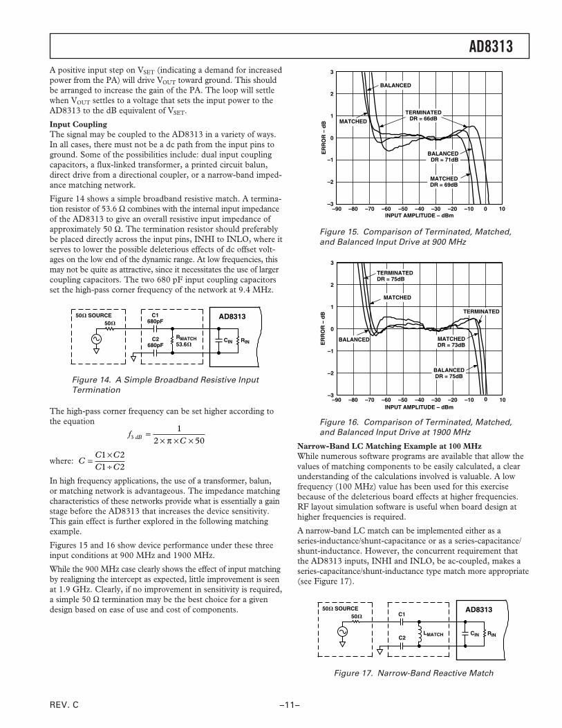
For high frequency use, Figure 8 shows the input impedanceplotted on a Smith chart. This measured result of a typicaldevice includes a 191 mil 50 W trace and a 680 pF capacitor toground from the INLO pin.
1.1pF900�1.9GHz
Frequency100MHz900MHz1.9GHz2.5GHz
R650552223
+ j X– j 400– j 135– j 65– j 43
AD8313 MEASURED
2.5GHz
900MHz
100MHz
Figure 8. Typical Input Impedance
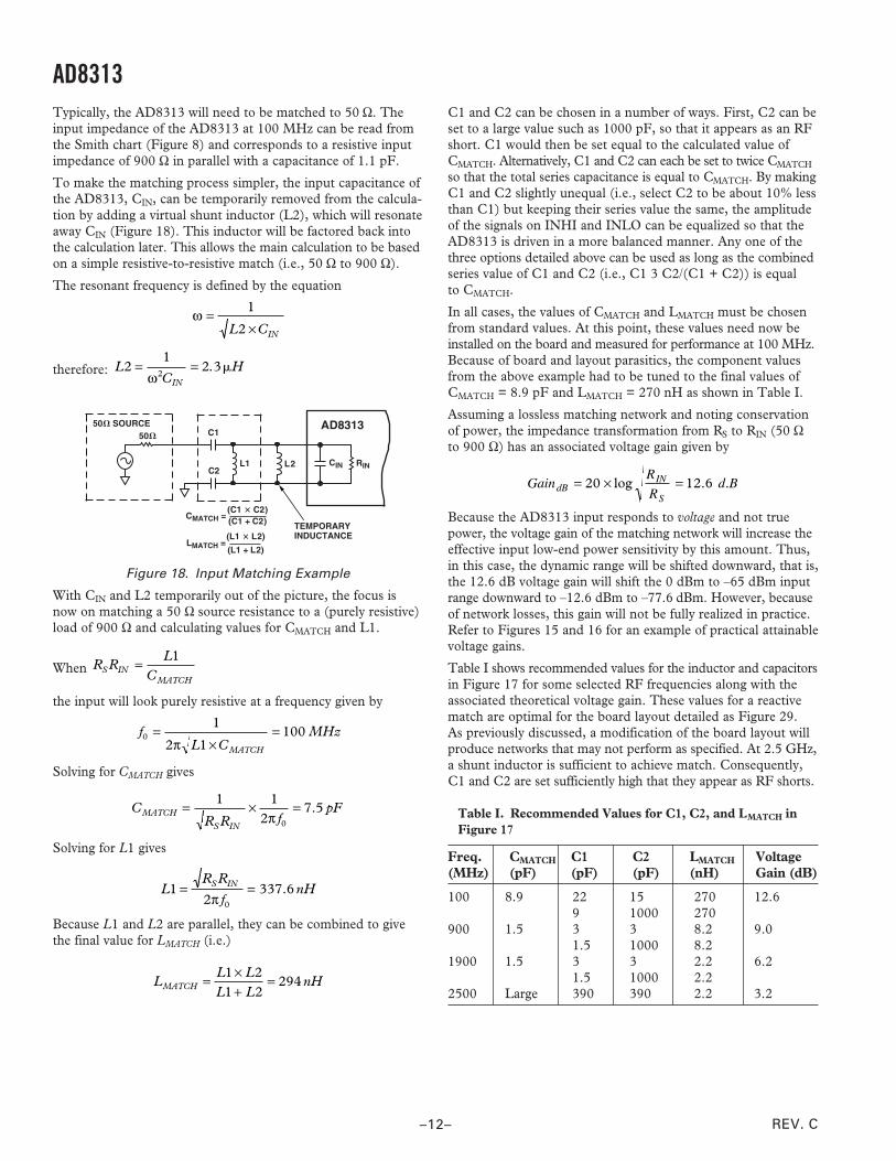
Logarithmic/Error Output, VOUTThe rail-to-rail output interface is shown in Figure 9. VOUT canrun from within about 50 mV of ground, to within about 100 mVof the supply voltage, and is short-circuit safe to either supply.However, the sourcing load current ISOURCE is limited to thatprovided by the PNP transistor, typically 400 mA. Larger loadcurrents can be provided by adding an external NPN transistor(see Applications). The dc open-loop gain of this amplifier is high,and it may be regarded as essentially an integrator having acapacitance of 2 pF (CINT) driven by the current-mode signalgenerated by the summed outputs of the nine detector stages,which is scaled approximately 4.0 mA/dB.
COMM
gm STAGE
CINTLP
LM10mAMAX
VOUT
CL
BIASISOURCE400�A
VPOS
FROMSETPOINT
SUMMEDDETECTOR
OUTPUTS
6
8
1
Figure 9. Output Interface Circuitry
Thus, for a midscale RF input of about 3 mV, which is some 40 dBabove the minimum detector output, this current is 160 mA, andthe output changes by 8 V/ms. When VOUT is connected to VSET,the rise and fall times are approximately 40 ns (for RL ≥ 10 kW).

AD8313
–10– REV. C
The nominal slew rate is ± 2.5 V/ms. The HF compensationtechnique results in stable operation with a large capacitive load,CL, though the positive-going slew rate will then be limited byISOURCE/CL to 1 V/ms for CL = 400 pF.
Setpoint Interface, VSETThe setpoint interface is shown in Figure 10. The voltage VSET
is divided by a factor of 3 in a resistive attenuator of 18 kW totalresistance. The signal is converted to a current by the action ofthe op amp and the resistor R3 (1.5 kW), which balances thecurrent generated by the summed output of the nine detector cellsat the input to the previous cell. The logarithmic slope is nomi-nally 3 � 4.0 mA/dB � 1.5 kW ª 18 mV/dB.
VSET
VPOS
R112k�
COMM
FDBKTO O/PSTAGE
1
R26k�
R31.5k�
25�A25�A
8
6
LP
Figure 10. Setpoint Interface Circuitry
APPLICATIONSBasic Connections for Log (RSSI) ModeFigure 11 shows the AD8313 connected in its basic measurementmode. A power supply of 2.7 V to 5.5 V is required. The powersupply to each of the VPOS pins should be decoupled with a 0.1 mFsurface-mount ceramic capacitor and a series resistor of 10 W.
The PWDN pin is shown as grounded. The AD8313 may bedisabled by a logic high at this pin. When disabled, the chip cur-rent is reduced to about 20 mA from its normal value of 13.7 mA.The logic threshold is at VPOS/2, and the enable function occursin about 1.8 ms; note, however, that further settling time is gen-erally needed at low input levels. While the input in this case isterminated with a simple 50 W broadband resistive match, thereis a wide variety of ways in which the input termination can beaccomplished. These are discussed in the Input Coupling section.
VSET is connected to VOUT to establish a feedback path thatcontrols the overall scaling of the logarithmic amplifier. Theload resistance, RL, should not be lower than 5 kW in order thatthe full-scale output of 1.75 V can be generated with the limitedavailable current of 400 mA max.
As stated in the Absolute Maximum Ratings, an externally appliedovervoltage on the VOUT pin that is outside the range 0 V to VPOS
is sufficient to cause permanent damage to the device. If over-voltages are expected on the VOUT pin, a series resistor (RPROT)should be included as shown. A 500 W resistor is sufficient toprotect against overvoltage up to ± 5 V; 1000 W should be used ifan overvoltage of up to ± 15 V is expected. Since the output stageis meant to drive loads of no more than 400 mA, this resistor willnot impact device performance for more high impedance driveapplications (higher output current applications are discussed inthe Increasing Output Current section).
R210�
RL = 1M�0.1�F
53.6�680pF
680pF
R110�
0.1�F
+VS
+VS
8
7
6
5
1
2
3
4
VPOS VOUT
INHI
INLO
VPOS PWDN
COMM
VSETAD8313
RPROT
Figure 11. Basic Connections for Log (RSSI) Mode
Operating in Controller ModeFigure 12 shows the basic connections for operation in controllermode. The link between VOUT and VSET is broken and a set-point is applied to VSET. Any difference between VSET and theequivalent input power to the AD8313 will drive VOUT either to thesupply rail or close to ground. If VSET is greater than the equiva-lent input power, VOUT will be driven toward ground, and vice versa.
VSETPOINTINPUT
CONTROLLEROUTPUT
R310�
0.1�F
R110�
0.1�F
+VS
+VS
8
7
6
5
1
2
3
4
VPOS VOUT
INHI
INLO
VPOS PWDN
COMM
VSET
RPROT
AD8313
Figure 12. Basic Connections for Operation in theController Mode
This mode of operation is useful in applications where the outputpower of an RF power amplifier (PA) is to be controlled by ananalog AGC loop (Figure 13). In this mode, a setpoint voltage,proportional in dB to the desired output power, is applied to theVSET pin. A sample of the output power from the PA, via a direc-tional coupler or other means, is fed to the input of the AD8313.
SETPOINTCONTROL DAC
RFINVOUT
VSET
AD8313
DIRECTIONALCOUPLER
POWERAMPLIFIER
RF IN
ENVELOPE OFTRANSMITTEDSIGNAL
Figure 13. Setpoint Controller Operation
VOUT is applied to the gain control terminal of the power amplifier.The gain control transfer function of the power amplifier shouldbe an inverse relationship, i.e., increasing voltage decreases gain.
AD8313
–11–REV. C
A positive input step on VSET (indicating a demand for increasedpower from the PA) will drive VOUT toward ground. This shouldbe arranged to increase the gain of the PA. The loop will settlewhen VOUT settles to a voltage that sets the input power to theAD8313 to the dB equivalent of VSET.
Input CouplingThe signal may be coupled to the AD8313 in a variety of ways.In all cases, there must not be a dc path from the input pins toground. Some of the possibilities include: dual input couplingcapacitors, a flux-linked transformer, a printed circuit balun,direct drive from a directional coupler, or a narrow-band imped-ance matching network.
Figure 14 shows a simple broadband resistive match. A termina-tion resistor of 53.6 W combines with the internal input impedanceof the AD8313 to give an overall resistive input impedance ofapproximately 50 W. The termination resistor should preferablybe placed directly across the input pins, INHI to INLO, where itserves to lower the possible deleterious effects of dc offset volt-ages on the low end of the dynamic range. At low frequencies, thismay not be quite as attractive, since it necessitates the use of largercoupling capacitors. The two 680 pF input coupling capacitorsset the high-pass corner frequency of the network at 9.4 MHz.
RMATCH53.6�
C1680pF
C2680pF
CIN RIN
AD831350�
50� SOURCE
Figure 14. A Simple Broadband Resistive InputTermination
The high-pass corner frequency can be set higher according tothe equation
f
CdB31
2 50=
¥ ¥ ¥p
where: C
C CC C
=¥∏
1 21 2
In high frequency applications, the use of a transformer, balun,or matching network is advantageous. The impedance matchingcharacteristics of these networks provide what is essentially a gainstage before the AD8313 that increases the device sensitivity.This gain effect is further explored in the following matchingexample.
Figures 15 and 16 show device performance under these threeinput conditions at 900 MHz and 1900 MHz.
While the 900 MHz case clearly shows the effect of input matchingby realigning the intercept as expected, little improvement is seenat 1.9 GHz. Clearly, if no improvement in sensitivity is required,a simple 50 W termination may be the best choice for a givendesign based on ease of use and cost of components.
INPUT AMPLITUDE – dBm–80 –70 –60 –50 –40 –30 –20 –10
3
2
1
0
–1
–2
–3
ER
RO
R –
dB
TERMINATEDDR = 66dB
–90 100
BALANCED
MATCHED
BALANCEDDR = 71dB
MATCHEDDR = 69dB
Figure 15. Comparison of Terminated, Matched,and Balanced Input Drive at 900 MHz
INPUT AMPLITUDE – dBm–80 –70 –60 –50 –40 –30 –20 –10 0
3
2
1
0
–1
–2
–3
ER
RO
R –
dB
–90 10
TERMINATEDDR = 75dB
BALANCED
BALANCEDDR = 75dB
MATCHEDDR = 73dB
MATCHED
TERMINATED
Figure 16. Comparison of Terminated, Matched,and Balanced Input Drive at 1900 MHz
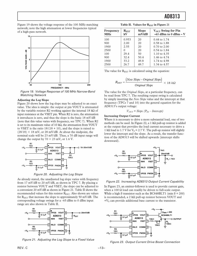
Narrow-Band LC Matching Example at 100 MHzWhile numerous software programs are available that allow thevalues of matching components to be easily calculated, a clearunderstanding of the calculations involved is valuable. A lowfrequency (100 MHz) value has been used for this exercisebecause of the deleterious board effects at higher frequencies.RF layout simulation software is useful when board design athigher frequencies is required.
A narrow-band LC match can be implemented either as aseries-inductance/shunt-capacitance or as a series-capacitance/shunt-inductance. However, the concurrent requirement thatthe AD8313 inputs, INHI and INLO, be ac-coupled, makes aseries-capacitance/shunt-inductance type match more appropriate(see Figure 17).
LMATCH
C1
C2CIN RIN
AD831350�
50� SOURCE
Figure 17. Narrow-Band Reactive Match
AD8313
–12– REV. C
Typically, the AD8313 will need to be matched to 50 W. Theinput impedance of the AD8313 at 100 MHz can be read fromthe Smith chart (Figure 8) and corresponds to a resistive inputimpedance of 900 W in parallel with a capacitance of 1.1 pF.
To make the matching process simpler, the input capacitance ofthe AD8313, CIN, can be temporarily removed from the calcula-tion by adding a virtual shunt inductor (L2), which will resonateaway CIN (Figure 18). This inductor will be factored back intothe calculation later. This allows the main calculation to be basedon a simple resistive-to-resistive match (i.e., 50 W to 900 W).
The resonant frequency is defined by the equation
w =¥1
2L CIN
therefore: L
CH
IN
21
2 32
= =w
. �
CMATCH =(C1 � C2)(C1 + C2)
LMATCH =(L1 � L2)
(L1 + L2)
C1
C2CIN RIN
AD831350�
50� SOURCE
L1 L2
TEMPORARYINDUCTANCE
Figure 18. Input Matching Example
With CIN and L2 temporarily out of the picture, the focus isnow on matching a 50 W source resistance to a (purely resistive)load of 900 W and calculating values for CMATCH and L1.
When R R
LCS IN
MATCH
= 1
the input will look purely resistive at a frequency given by
fL C
MHzMATCH
01
2 1100=
¥=
p
Solving for CMATCH gives
CR R f
pFMATCH
S IN
= ¥ =1 12
7 50p
.
Solving for L1 gives
L
R R
fnHS IN1
2337 6
0
= =p
.
Because L1 and L2 are parallel, they can be combined to givethe final value for LMATCH (i.e.)
L
L LL L
nHMATCH = ¥+
=1 21 2
294
C1 and C2 can be chosen in a number of ways. First, C2 can beset to a large value such as 1000 pF, so that it appears as an RFshort. C1 would then be set equal to the calculated value ofCMATCH. Alternatively, C1 and C2 can each be set to twice CMATCH
so that the total series capacitance is equal to CMATCH. By makingC1 and C2 slightly unequal (i.e., select C2 to be about 10% lessthan C1) but keeping their series value the same, the amplitudeof the signals on INHI and INLO can be equalized so that theAD8313 is driven in a more balanced manner. Any one of thethree options detailed above can be used as long as the combinedseries value of C1 and C2 (i.e., C1 3 C2/(C1 + C2)) is equalto CMATCH.
In all cases, the values of CMATCH and LMATCH must be chosenfrom standard values. At this point, these values need now beinstalled on the board and measured for performance at 100 MHz.Because of board and layout parasitics, the component valuesfrom the above example had to be tuned to the final values ofCMATCH = 8.9 pF and LMATCH = 270 nH as shown in Table I.
Assuming a lossless matching network and noting conservationof power, the impedance transformation from RS to RIN (50 Wto 900 W) has an associated voltage gain given by
Gain
R
Rd BdB
IN
S= ¥ =20 12 6log . .
Because the AD8313 input responds to voltage and not truepower, the voltage gain of the matching network will increase theeffective input low-end power sensitivity by this amount. Thus,in this case, the dynamic range will be shifted downward, that is,the 12.6 dB voltage gain will shift the 0 dBm to –65 dBm inputrange downward to –12.6 dBm to –77.6 dBm. However, becauseof network losses, this gain will not be fully realized in practice.Refer to Figures 15 and 16 for an example of practical attainablevoltage gains.
Table I shows recommended values for the inductor and capacitorsin Figure 17 for some selected RF frequencies along with theassociated theoretical voltage gain. These values for a reactivematch are optimal for the board layout detailed as Figure 29.As previously discussed, a modification of the board layout willproduce networks that may not perform as specified. At 2.5 GHz,a shunt inductor is sufficient to achieve match. Consequently,C1 and C2 are set sufficiently high that they appear as RF shorts.
Table I. Recommended Values for C1, C2, and LMATCH in Figure 17
Freq. CMATCH C1 C2 LMATCH Voltage(MHz) (pF) (pF) (pF) (nH) Gain (dB)
100 8.9 22 15 270 12.69 1000 270
900 1.5 3 3 8.2 9.01.5 1000 8.2
1900 1.5 3 3 2.2 6.21.5 1000 2.2
2500 Large 390 390 2.2 3.2
AD8313
–13–REV. C
Figure 19 shows the voltage response of the 100 MHz matchingnetwork; note the high attenuation at lower frequencies typicalof a high-pass network.
FREQUENCY – MHz
15
50
VO
LT
AG
E G
AIN
– d
B
10
5
0
–5100 200
Figure 19. Voltage Response of 100 MHz Narrow-BandMatching Network
Adjusting the Log SlopeFigure 20 shows how the log slope may be adjusted to an exactvalue. The idea is simple: the output at pin VOUT is attenuatedby the variable resistor R2 working against the internal 18 kW ofinput resistance at the VSET pin. When R2 is zero, the attenuationit introduces is zero, and thus the slope is the basic 18 mV/dB(note that this value varies with frequency, see TPC 7). When R2is set to its maximum value of 10 kW, the attenuation from VOUTto VSET is the ratio 18/(18 + 10), and the slope is raised to(28/18) � 18 mV, or 28 mV/dB. At about the midpoint, thenominal scale will be 23 mV/dB. Thus, a 70 dB input range willchange the output by 70 � 23 mV, or 1.6 V.
18–30mV/dB
R210k�
R310�
0.1�F
R110�
0.1�F
+VS
+VS
8
7
6
5
1
2
3
4
VPOS VOUT
INHI
INLO
VPOS PWDN
COMM
VSETAD8313
Figure 20. Adjusting the Log Slope
As already stated, the unadjusted log slope varies with frequencyfrom 17 mV/dB to 20 mV/dB, as shown in TPC 7. By placing aresistor between VOUT and VSET, the slope can be adjusted toa convenient 20 mV/dB as shown in Figure 21. Table II shows therecommended values for this resistor REXT. Also shown are valuesfor REXT that increase the slope to approximately 50 mV/dB. Thecorresponding voltage swings for a –65 dBm to 0 dBm inputrange are also shown in Table II.
20mV/dB
REXT
R310�
0.1�F
R110�
0.1�F
+VS
+VS
8
7
6
5
1
2
3
4
VPOS VOUT
INHI
INLO
VPOS PWDN
COMM
VSETAD8313
Figure 21. Adjusting the Log Slope to a Fixed Value
Table II. Values for REXT in Figure 21
Frequency REXT Slope VOUT Swing for PinMHz kV mV/dB –65 dBm to 0 dBm – V
100 0.953 20 0.44 to 1.74900 2.00 20 0.58 to 1.881900 2.55 20 0.70 to 2.002500 0 20 0.54 to 1.84100 29.4 50 1.10 to 4.35900 32.4 50.4 1.46 to 4.741900 33.2 49.8 1.74 to 4.982500 26.7 49.7 1.34 to 4.57
The value for REXT is calculated using the equation:
R
New Slope Original Slope
Original SlopeEXT =
( )– � 18 kW
The value for the Original Slope, at a particular frequency, canbe read from TPC 7. The resulting output swing is calculatedby simply inserting the New Slope value and the intercept at thatfrequency (TPCs 7 and 10) into the general equation for theAD8313’s output voltage:
VOUT = Slope (PIN – Intercept)
Increasing Output CurrentWhere it is necessary to drive a more substantial load, one of twomethods can be used. In Figure 22, a 1 kW pull-up resistor is addedat the output that provides the load current necessary to drive a1 kW load to 1.7 V for VS = 2.7 V. The pull-up resistor will slightlylower the intercept and the slope. As a result, the transfer func-tion of the AD8313 will be shifted upwards (intercept shiftsdownward).
R210�
0.1�F
R110�
0.1�F
+VS
+VS
1
2
3
4
VPOS VOUT
INHI
INLO
VPOS PWDN
COMM
VSET
8
7
6
5
AD8313 RL = 1k�
20mV/dB
1k�
+VS
Figure 22. Increasing AD8313 Output Current Capability
In Figure 23, an emitter-follower is used to provide current gain,when a 100 W load can readily be driven to full-scale output.While a high ß transistor such as the BC848BLT1 (min ß = 200)is recommended, a 2 kW pull-up resistor between VOUT and+VS can provide additional base current to the transistor.
R310�
0.1�F
R110�
0.1�F
+VS
+VS
8
7
6
5
1
2
3
4
VPOS VOUT
INHI
INLO
VPOS PWDN
COMM
VSETAD8313 OUTPUT
+VS
13k�
RL100�
10k�
BC848BLT1
�MIN = 200
Figure 23. Output Current Drive Boost Connection

AD8313
–14– REV. C
In addition to providing current gain, the resistor/potentiometercombination between VSET and the emitter of the transistorincreases the log slope to as much as 45 mV/dB, at maximumresistance. This will give an output voltage of 4 V for a 0 dBminput. If no increase in the log slope is required, VSET can beconnected directly to the emitter of the transistor.
Effect of Waveform Type on InterceptAlthough it is specified for input levels in dBm (dB relative to1 mW), the AD8313 fundamentally responds to voltage and notto power. A direct consequence of this characteristic is thatinput signals of equal rms power but differing crest factors willproduce different results at the log amp’s output.
The effect of different signal waveforms is to vary the effectivevalue of the log amp’s intercept upward or downward. Graphically,this looks like a vertical shift in the log amp’s transfer function.The device’s logarithmic slope, however, is in principle not affected.For example, consider the case of the AD8313 being alternatelyfed from a continuous wave and a single CDMA channel of thesame rms power. The AD8313’s output voltage will differ by theequivalent of 3.55 dB (64 mV) over the complete dynamic rangeof the device (the output for a CDMA input being lower).
Table III shows the correction factors that should be applied tomeasure the rms signal strength of a various signal types. A continu-ous wave input is used as a reference. To measure the rms powerof a square wave, for example, the mV equivalent of the dBvalue given in the table (18 mV/dB times 3.01 dB) should besubtracted from the output voltage of the AD8313.
Table III. Shift in AD8313 Output for Signals with DifferingCrest Factors
Correction FactorSignal Type (Add to Output Reading)
CW Sine Wave 0 dBSquare Wave or DC –3.01 dBTriangular Wave +0.9 dBGSM Channel (All Time Slots On) +0.55 dBCDMA Channel +3.55 dBPDC Channel (All Time Slots On) +0.58 dBGaussian Noise +2.51 dB
EVALUATION BOARDSchematic and LayoutFigure 28 shows the schematic of the evaluation board that wasused to characterize the AD8313. Note that uninstalled compo-nents are drawn in as dashed.
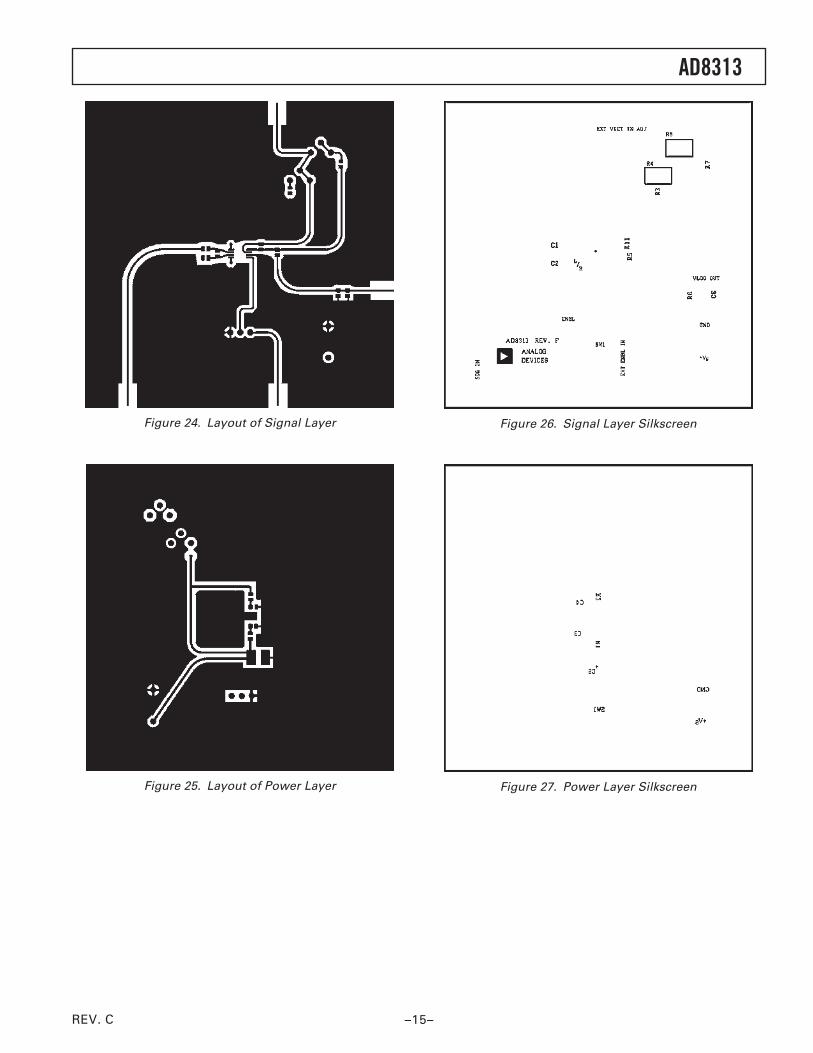
This is a 3-layer board (signal, ground, and power), with aDuroid dielectric (RT 5880, h = 5 mil, eR = 2.2). FR4 can also beused, but microstrip dimensions must be recalculated becauseof the different dielectric constant and board height. The tracelayout and silkscreen of the signal and power layers are shown inFigures 24 to 27. A detail of the PCB footprint for the MSOPpackage and the pads for the matching components are shownin Figure 29.
The vacant portions of the signal and power layers are filled outwith ground plane for general noise suppression. To ensure alow impedance connection between the planes, there are mul-tiple through-hole connections to the RF ground plane. Whilethe ground planes on the power and signal planes are used asgeneral-purpose ground returns, any RF grounds related to theinput matching network (e.g., C2) are returned directly to theRF internal ground plane.
General OperationThe board should be powered by a single supply in the range of2.7 V to 5.5 V. The power supply to each of the VPOS pins isdecoupled by a 10 W resistor and a 0.1 mF capacitor.
The two signal inputs are ac-coupled using 680 pF high qualityRF capacitors (C1, C2). A 53.6 W resistor across the differentialsignal inputs (INHI, INLO) combines with the internal 900 Winput impedance to give a broadband input impedance of 50.6 W.This termination is not optimal from a noise perspective due tothe Johnson noise of the 53.6 W resistor. Neither does it accountfor the AD8313’s reactive input impedance nor for the decreaseover frequency of the resistive component of the input impedance.However, it does allow evaluation of the AD8313 over its com-plete frequency range without having to design multiple matchingnetworks.
For optimum performance, a narrow-band match can be imple-mented by replacing the 53.6 W resistor (labeled L/R) with anRF inductor and replacing the 680 pF capacitors with appropri-ate values. The Narrow-Band LC Matching Example sectionincludes a table of recommended values for selected frequenciesand explains the method of calculation.
Switch 1 is used to select between power-up and power-downmodes. Connecting the PWDN pin to ground enables normaloperation of the AD8313. In the opposite position, the PWDNpin can either be driven externally (SMA connector labeledEXT ENABLE) to either device state or allowed to float to adisabled device state.
The evaluation board ships with the AD8313 configured tooperate in RSSI measurement mode, the logarithmic outputappearing on the SMA connector labeled VOUT. This mode isset by the 0 W resistor (R11), which shorts the VOUT andVSET pins to each other.
Varying the Logarithmic SlopeThe slope of the AD8313 can be increased from its nominal valueof 18 mV/dB to a maximum of 40 mV/dB by removing R11, the0 W resistor, which shorts VSET to VOUT. VSET and VOUTare now connected through a 20 kW potentiometer.
Operating in Controller ModeTo put the AD8313 into controller mode, R7 and R11 shouldbe removed, breaking the link between VOUT and VSET. TheVSET pin can then be driven externally via the SMA connectorlabeled EXT VSET IN ADJ.
Increasing Output CurrentTo increase the output current of VOUT, set both R3 and R11 to0 W and install potentiometer R4 (1 kW to 5 kW).
AD8313
–15–REV. C
Figure 24. Layout of Signal Layer
Figure 25. Layout of Power Layer
Figure 26. Signal Layer Silkscreen
Figure 27. Power Layer Silkscreen

AD8313
–16– REV. C
C2680pF
C1680pF
R210�
C30.1�F
R110�
+VS
+VS
1
2
3
4
VPOS VOUT
INHI
INLO
VPOS PWDN
COMM
VSET
AD83138
7
6
5
L/R53.6�
C40.1�F
SIG IN
R110�
R70�
R820k�
R3
R4
+VS
R50�
R6 C6
VOUT
EXT VSET
EXT ENABLE
SW1
Figure 28. Evaluation Board Schematic
4854.4
90.6
28
20
27.5
75 50
20
19
50
35
41 22
46
4851.7
91.3
51
10
16
126
TRACE WIDTH15.4
NOT CRITICAL DIMENSIONS
UNIT = MILS
Figure 29. Detail of PCB Footprint for Package and Pads for Matching Network
AD8313
–17–REV. C
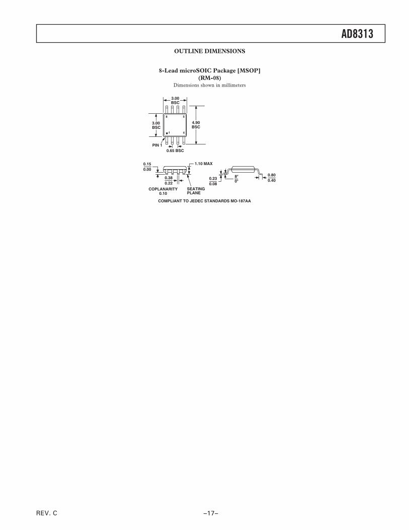
OUTLINE DIMENSIONS
8-Lead microSOIC Package [MSOP](RM-08)
Dimensions shown in millimeters
0.230.08
0.800.40
8�0�
8 5
41
4.90BSC
PIN 10.65 BSC
3.00BSC
SEATINGPLANE
0.150.00
0.380.22
1.10 MAX
3.00BSC
COMPLIANT TO JEDEC STANDARDS MO-187AA
COPLANARITY0.10

AD8313
–18– REV. C
Revision HistoryLocation Page
2/03—Data Sheet changed from REV. B to REV. C.
TPCs and Figures Renumbered .......................................................................................................................................... Universal
Edits to SPECIFICATIONS ...........................................................................................................................................................2
Updated ESD CAUTION ...............................................................................................................................................................4
Updated OUTLINE DIMENSIONS.............................................................................................................................................17

–19–

–20–
C01
085–
0–2/
03(C
)P
RIN
TE
D IN
U.S
.A.