a low leakage down-conversion k-band mixer using current
TRANSCRIPT

A Low Leakage Down-conversion K-Band MIXER using
Current-Reuse Double-Balanced Architecture in 130-nm
CMOS Process for Modern RF Applications
Zohaib Hasan Khan1, Shailendra Kumar
2 and Deepak Balodi
3
1,2Integral University, Lucknow 3BBD Engineering College, Lucknow, [email protected]
Abstract- A low noise and high conversion gain mixer is presented in this work which is effectively utilizing the
differential biasing condition, separately for the transconductance stage and the switching stage, due to the folded
double-balanced current reuse design. This has provided a great opportunity to work on the noise performance by
reducing the noise figure separately for both stages. The mixer’s architecture has been planned initially for the C-band
and has been tested for the same, then the design parameters have been scaled with the same topology for the K- band
(23 to 25 GHz). In this range of RF bandwidth, the proposed mixer’s architecture shows the highest conversion gain
of 24.2 dB, additionally with an excellent noise performance (noise figure of 7.9 dB) where a -3 dBm signal power has
been fed from the local oscillator (LO). A higher extent of linearity has also been achieved with the 1-dB compression
point of -17.8 dBm at the RF frequency of 24 GHz. From 23 to 25 GHz, the LO-to-RF, LO-to-IF isolations are
approximately 36 dB and 30 dB, respectively. Implemented double balance current reuse architecture of the proposed
mixer shows a power dissipation of 26.8 mW with a relatively higher power supply bias of 2.5 V. All the simulations
have been performed on Advanced Design System (Keysight Technology) with 130 nm RF-CMOS (UMC) technology.
Keywords- Conversion gain, noise figure, CMOS, down-conversion mixer, folded architecture, current-reuse, k-band
I. INTRODUCTION
The wireless components in the RF-CMOS domain which are used for direct-conversion architectures,
not only offer a compact-sized mobile terminal but also pave the wave for a low-cost RF solution (in
terms of both, software and hardware) using optimum power. Also, for bandwidth and modern
spectrum versatility, wideband RF CMOS components are expected to remain compatible with high
data-rate applications, such as 3G, 4G and 5G wireless communications (especially WLAN as
Bluetooth and WiFi), and multi-standard applications. For such a wide range of applications, the noise
of the RF components needs to be designed as low as possible as a significantly high SNR (Signal to
Noise Ratio) performance is sought by the end-to-end mobile units. Mixer’s architecture, used in the
RF transceiver for frequency mixing, could be active or passive depending upon the components and
circuit topology used in the design. Active mixes are more attractive and therefore preferred in most
of the wireless applications, due to their better conversion gain (relatively much higher than passive
counterpart). They also have the ability to suppress the noise which is being contributed by the stages
post-mixer placement in the receiver chain. Gilbert cell architecture (transconductor with switch:
GmSw) and switching-transconductance (SwGm) architectures are the two major types of active
down-conversion mixers [1]. In the Gilbert cell mixer, a large LO signal is fed to the transconductance

stage which then mixes with the tail RF current of the same transconductance stage working like a
switch, and produces the frequency conversion from RF to IF port.
Nowadays, CMOS technology is widely used for most RF building blocks implementation.
Especially, in RF receivers for modern wireless communication systems, all of the active RF building
blocks are implemented by CMOS technology. It is because that the CMOS technology is capable of
integration with a baseband chipset and offers low-cost implementation [2]. Therefore, the CMOS
technology and the direct-conversion architecture are welcomed for their great versatility and cost-
effective viewpoint. However, the commercialization of low-noise CMOS RF receiver with the direct
conversion architecture has not been easily achieved by the intrinsic drawbacks of standard CMOS
processes in RF perspectives, that is, a low transconductance, low unit gain frequency (fT), and high
flicker noise [3, 4]. The low values of transconductance and fT provide high thermal noise. The
implementation of a low flicker noise CMOS mixer is the efficient and sole way for low flicker noise
RF receiver. Lots of work and literature have been reported so far, where the efforts have been placed
to predict and model the behavior of the noise impact (mainly thermal noise and flicker noise) involved
in the operation of Gilbert cell mixer’s architecture [2-6]. Most of the modern RF design trends show
a simultaneous and parallel arrangement of several single band RF front ends to achieve an overall
multiband operation [7]. This gives a significant rise to the number of RF components in the
architecture as they are being replicated for different RF bands but with similar topology. This finally
increases the total power dissipation, the physical size of the system and the overall cost of the RF
front end design. A contemporary and more optimized approach is to use a single RF front-end
architecture for multiband operation, where each band is used one by one in a reuse concept [8]. This
requires a rigorous hardware reuse topology by bands and strict protocols but increases the hardware
efficiency to a greater extent. This approach is also appealing for millimetre-wave (mmW) transceivers
on silicon to increase the versatility, save the chip area, and reduce power consumption.
This paper consists of the qualitative analysis of the modern RF down-conversion mixers and
presents an optimum solution with double balanced current reuse architecture. Section II discusses
various challenges in the RF receiver architectures and constraints to the conventional mixers’
topologies. Section III depicts three major aspects of the multi-band down-conversion mixer
architectures, namely high conversion gain, sub-harmonic dual-band operation and current reuse
cross-coupled double-balanced operation. This work tries to incorporate all these aspects and proposes
a double-balanced cross-coupled architecture in 130 nm RF-CMOS (UMC) technology. High linearity
has also been attempted to achieve with high transconductance differential pair (with larger
dimensions) and a higher 1-dB compression point is targeted. Section IV finally presents the proposed
mixer architecture, which offers the optimum performance on the above-said aspects. Transient
analysis and harmonic balance simulations have been performed to investigate the mixing behaviour
and linearity assessment. The successful mixing behaviour with high linearity and optimum noise
cancellation establish the usefulness of the proposed double-balanced down conversion mixer
architecture.

II. BASIC ASPECTS & TOPOLOGIES OF RF MIXER
There are also various forms of RF mixer that need to be understood. One of the first relates to the
type of electronic components or devices within the mixer:
(a) Passive mixers: Various conventional passive mixer architectures are available, which typically
have no gain, but instead provide better isolation and implementation. In most of the passive
architectures, Schottky diodes are used as the switching element, having an additional low turn-on
voltage advantage. For this, they need balanced transformers for most high-performance designs
and this can limit the frequency band over which they can operate [1-3]. One key aspect of passive
mixers is that they introduce what is called a conversion loss, explained later, and this can have an
impact on the RF circuit design.
(b) Active mixers: Transistors are used as electronic switching element, providing the essential
mixing operation. The significant advantage of active architecture is a high gain with reasonable
isolation. Unlike passive mixers, active mixers can have a conversion gain, and this will affect the
RF design for the item [3].
RF mixers or frequency mixers can also be categorized according to whether they are balanced or
unbalanced. This is an important decision to make.
Unbalanced: An unbalanced RF mixer is a basic form of RF mixer which performs the
fundamental task of mixing and provides sum and difference of the two input signals to it (RF
input and LO input). Output also comprises a significant amplitude of original RF signal in
addition with oscillator’s component, which in turn results in poor isolation [16, 24]. As there is
little isolation between the ports this can lead to increased levels of intermodulation distortion as
well as the local oscillator and RF signals being present on the output.
Balanced: A balanced mixer is one in which the ports have a balanced or differential structure.
Dependent upon the actual type there can be isolation between the different ports, and the LO and
RF can be suppressed at the IF port. There are different types of balanced mixer: single balanced;
double-balanced and triple balanced (more correctly termed a doubly double-balanced mixer).
Figure 1: RF Mixer model with associated leakage and feedthrough problem

The isolation level between the ports is often important and it states the level of what may be
termed the leakage between the different ports. The RF and local oscillator are not normally needed
at the IF, and if, for example, the local oscillator leaks through to the RF port, it could give rise to
intermodulation distortion (Figure 1). As might be expected the isolation is measured in terms of dB,
comparing the signal entering one port, to the same signal level at the other port where it is not
required. It is found that mixer isolation tends to deteriorate with increasing frequency as the reactance
of stray capacitance falls, and also the circuit imbalances become more apparent [24, 25]. One major
issue with any RF mixer is the level of unwanted signals that are generated within the mixing process.
Non-linearities within the mixer give rise to additional signals and these can cause issues in many
ways dependent upon the circuit design or system in which they are used. The third-order intercept
point of a mixer (or amplifier) is a hypothetical point where the power of the third-order products will
have the same power level as the fundamental. The third-order intercept point of a mixer of any other
device is theoretical because it lies well beyond the saturation level of the device, and in many cases,
it would be well beyond the point at which damage occurred, especially in the case of a mixer. The
reason that the IP3 figure is useful is that it provides a very good guide or figure of merit for the
distortion generated by the device as the power levels rise.
III. RELATED WORK AND CHALLENGES IN MODERN RF MIXER DESIGNS
The section demonstrates the advanced architecture of the RF down-conversion mixers and the related
challenges. The related efforts and publications are also mentioned along with. An optimum design to
tackle these issues will be then evolved in the next section.
A. Sub-Harmonic and Fundamental Frequency-based Dual Band Operation
The most attractive and useful component in the RF multi-band front-end structure is the multi-band
mixer where the noise performance is a critical factor. In [9], a dual-band mixer was proposed where
the mixer’s architecture uses a matching network. This comprises the switched inductor topology and
the inductor size has been chosen wisely to fit the frequency range of interest. In another similar effort
[10], an LC matching network was used for the dual-band operation where the two frequency bands
of interest are being served by the proposed mixer’s topology. In addition to this, a combination of
composite right-left handed transmission lines was also used [11] to implement a dual-band mixer. In
all the above-said efforts, multiple local oscillators (LOs) were used for multiband operations. On the
other side, a novel approach in [12] offers a dual-band self-oscillating mixer topology, where the
fundamental and the second harmonic of the LO was used to mix with the set of complementary
switches. In another similar effort [13], the third harmonic component of LO in addition to the
fundamental was used for the mixing with the input signal to get the desired band selection at the IF
port. Reconfigurability to the spectrum has been an attractive tool to bring in flexibility in the
performance of the RF system like mixers, antenna and Low Noise Amplifiers (LNAs). Similar
reconfigurability was attempted using a passive Sub- Harmonic Mixer (SHM), where a ring oscillator
with multi-stage injection locking was used to generate several phases of the LO signals [14]. After

the selection of an appropriate LO phase, finally, the mixer was reconfigured in between the
subharmonic operation and the fundamental operational modes.
B. High Conversion Gain RF Mixers for K-band applications (Gain-Boosted)
The major job of a down-conversion mixer is to get the RF signal at the input and mix it with the LO
signal and finally provide the intermediate frequency signal at the output. A high LO voltage signal is
generally sought to minimize the conversion losses which are mainly associated with a passive
structure of the down-conversion mixer this ultimately downgrades the performance of the mixer and
imposes a difficult constraint on the LO structure design. This also incurs high-power dissipation
losses. This demand for an active down-conversion mixer also invites the low noise figure, high
linearity and better isolation from various ports in addition to the high conversion gain. These
requirements become more stringent if the application shifts to a higher frequency side like a K band
or Ku band application. However, various technological aspects like Silicon leakage losses,
technology integration and low quality (Q) passive components makes it difficult to achieve the high
conversion gain, low noise figure and better isolation for K band mixers.
Lots of efforts have been made to tackle the aforementioned challenges in the area of down-
conversion CMOS mixer design. The conventional current bleeding technique has been used by
Chang, et al. and Lin, et al. respectively for a k band mixer in a 180 nm CMOS process. K-band down-
conversion mixers with current-bleeding technique in 0.18-µm CMOS [16], [19]. A high conversion
gain of 8.4 dB with the noise figure of 11.6 dB achieved has been achieved in the work offered [16].
The other proposal [17, 19] also demonstrated k -band down-conversion mixer in the 180-nm CMOS
process which provided the improved linearity of -13.6 dBm IP1 and a high conversion gain of 10.7
dB. Using the PMOS cross-coupled pair as an active load in 0.18-µm CMOS, Chang, et al.
demonstrated a K-band down-conversion mixer with the measured peak CG of 11.9 dB at 23 GHz and
a -3-dB bandwidth of 7 GHz [18]. Recently Yao Peng, Jin He et al. [20] presented a new K-band
down-conversion mixer, which has been designed and fabricated using a 130-nm RF CMOS process.
A common problem is to have the same biasing for both the transconductance stage as well as switch
stage in differential topology, which offers the limitation to the gm of the transconductance stage. This
is improved by the folded double-balanced architecture of the mixers in which the bias circuitry is
different for the transconductance and switch stages and hence the transconductance stage is separately
biased for a high gm. This improves the noise reduction significantly, without having much impact on
the bias circuit of the switch stage. In addition to this, the current reuse technique greatly improves the
transconductance of the gm stage, and a cross-coupled structure offers high active loading. This in
addition to the aforementioned benefit, greatly improves the conversion gain (High CG) and noise
figure (Low NF) of the down-conversion mixer.
C. Current Reuse using Cross-Coupled Technique for Double-Balanced Structures
In RF front end blocks, LO noise propagates progressively and reaches to the IF output. A common
practice to tackle this problem significantly, is to opt for differentially balanced architecture which

suppresses the noise propagation to the later stages. A balanced mixer uses a four-port hybrid junction
as shown in Figure 2.
Figure 2: A balanced mixer topology
Input terminal of a balanced architecture is fed with LO and RF signals, as shown in Figure 2.
The remaining two ports consists of diode as switching element. The balanced connection is made
such that, at the input of one diode receives the sum of LO and RF, whereas another diode processes
the difference between the two. One stringent requirement for the successful mixing under balanced
criterion is that both the diodes must possess exactly the same characteristics with close matching. As
the LO noise remains in phase at both the diodes, it gets cancelled, and level of cancellation strongly
depends upon the matching of the nonlinear devices (diodes here). It is often advantageous to also
provide balanced connections to the local oscillator, in which case the mixer is said to be double-
balanced, or even to both the input signal and local oscillator (a triple-balanced mixer). Now, as
switching nonlinear elements possess the finite conducting losses, this in turn degrades the conversion
gain and the value differs significantly from the idealistic mark. Amplitude of LO signal also impacts
the conversion gain significantly, as it is cause behind ON and OFF switching of the nonlinear mixing
elements. A higher amplitude of LO signal provides a higher conversion gain but at the cost of more
power dissipation. Real (passive) microwave mixers usually have conversion loss varying from about
6 dB to 11 dB. Figure 3 depicts the conventional folded double-balanced architecture of a down-
conversion mixer, in which transconductance and load stages are mentioned separately.
The original unbalanced external inputs have to be first converted to the balanced mode, for
which RF and LO baluns have been implemented using the on-chip transformers. The complementary
pairs of M1-M2 and M3-M4 are used in the inverter topology which finally provide the current reuse
phenomena and thereby give the high transconductance gain gm. The additional advantage of noise in
terms of input-referred noise is obtained due to the inverting pairs for the differential transistors of the
RF stage. Transistors M5-M8 constitute the switch stage which is being fed by the RF signals from
the differential architecture. These LO signals are already obtained in the balance mode by the input
balun. The required driving LO power is significantly reduced by maximizing the sizes of the
transistors M5 to M8 which build the switch stage, as they are being driven by the low overdrive gate
voltages [21]. A passive T-section is implemented and connected at the common switching node of

the switch which is made up of LC (inductors L1 and L2 and a bypass capacitor C0) components. This
serves the improvisation in the conversion gain using the resonant mode of L1 and L2 with the parasitic
capacitances at the operating frequency and reduces the leakage of the differential RF currents (thereby
reducing noise figure) with compensation of gate-drain capacitances of transistors M1-M4 [22]. The
LO to RF leakage is significantly reduced due to this and better isolation is achieved [23, 24].
Figure 3: Folded double-balanced down conversion mixer
A very high-quality factor is aimed to be achieved while implementing the inductors L1 and L2
at the frequency of 24 GHz. An active load stage with very high equivalent load impedance is required
to obtain the high conversion gain which is obtained by the cross-coupled pairs implemented with
M11-R9 and M12-R10. Finally, the transistors M9 and M10 are serving the current biasing phenomena
which are directly biased with VB4 to source the current. To make the IF port free from loading effects
and achieve a strong driving phenomenon, the self-bias inverting mode amplifiers are implemented
using transistors M13 to M16 with the feedback resistors R7 and R8.
The above detailing and explanation of the current reuse cross-coupled differential structure
for the mixing phenomenon makes the understanding of the topology very clear and helps in
improvisation of the architecture [25, 26]. This also explained all the major constraints related to the
important parameters like conversion gain, isolation, leakage and noise reduction.

D. Noise Cancelling Architectures
Evaluation of noise performance in the case of the mixer becomes significantly important as the blocks
ahead of it have a severe constraint on the noise component of the signal. The noise contribution from
the mixer architecture comes while they perform a multiplication process (in the time domain) or
frequency conversion (in the frequency domain). The main signal power as well as the noise signal
both get amplified, attenuated or filtered by the mixer characteristic (using either conversion gain or
frequency selectivity of the mixer). But the Omnipresent character of the noise depicted by its white
distribution in the frequency domain makes the output signal vulnerable [27]. Most importantly, a
significant amount of additional noise is contributed from the active solid-state devices used in the
mixer architecture design.
This noise performance of the mixer and other RF components is generally measured in terms of noise
figure which is defined as the proportion of signal-to-noise ratios (SNRs) from input to output [27,
28]. In the specific case of a down-conversion mixer the noise figure could be defined in two ways:
using SSB noise figure; or considering the DSB noise figure [29]. In the case of the SSB noise figure,
the noise component of the RF signal is taken down from both the upper and lower sideband whereas
the signal component is translated only from the single-sideband (as the other one is considered to be
an image). Opposite to this in the case of the DSB noise figure the signal, as well as noise both, are
considered to be translated down for the noise figure evaluation. Therefore, total signal power is
doubly impacted by the noise in the case of the SSB noise figure as there is no RF counterpart for the
remaining sideband. This in turn provides a noise figure 3dB more for the SSB-NF definition as
compared to DSB. The matching interfaces are also equally important in the RF system design other
than the noise figure, hence the input-referred noise voltage is also an important parameter for the
noise evaluation. The noise figure formula provided by Friis [28, 30] for the cascaded systems proves
to be an important tool for power defining signal values. Mixers usually have a poor noise performance
with the noise figure ranging from 6 to 10 dB. This is a consequence of the signal loss in the switching,
but also of noise being transferred from multiple frequency bands to the output, as shown in Figure 4.
Figure 4: Noise folding phenomenon in mixer operation
An idealized signal generator is expected to assist the mixer, as practically an LO signal
generators have certain significant sidebands other than the desired impulse spectrum, which later on
folds the noise to the IF or baseband of the output signal of the mixer. Due to this most of the circuit
designers consider the LO design as a part of the complete mixer’s architecture design. For example,
the switching loss in a double balance architecture of a mixer remains in the range of 3-4 dB, whereas
due to the LO signal noise impact it increases a few decibels higher and reaches around 5-6 dB. The
overall noise evaluation in a mixer could be done at three stages first at the input stage, secondly at
the main switching stage which consists of the mixer’s architecture, and lastly the output stage of the
IF port. Due to the frequency mixing phenomena of the mixer’s operation, its characteristic is not
straightforward and rather becoming time-varying. This time-varying behaviour makes the noise
calculation and evaluation a little bit cumbersome.
Constant current bias injection has been a prominent approach to reduce the current impact by
deteriorating the noise current pulses trying to appear at the output. Several mechanisms and
approaches in this regard have been tried and published [24, 25, 26, and 27]. Whereas, applying the
current pulses specifically at the switching instances significantly improves the noise controlling into
the switching and mixing circuits’ outputs and hence known as dynamic current injection [28]. Current
pulses from the switching pairs of the input circuits are also suppressed to a greater extent. The
equivalent tail node capacitance in the differential pair structure imposes its noise contribution which
could not be suppressed via this mechanism hence remains as a point of consideration. To tackle this
situation, an inductive approach has been adopted which compensates for the capacitive noise injection
in the modern RF circuits by introducing the resonating behaviour with this parasitic capacitive node.
Specifically, Gilbert cell mixers are employing the inductors at the tail node, to control the static and
dynamic current injection which otherwise couples the noise into it [26, 29, 30]. But the circuit
architectures with inductor implementation impose compatibility and chip area issues, as the inductor
design consumes a lot of silicon area. Sometimes a negative impedance circuit is used in the mixer
design where the capacitor in negative feedback offers an active inductive loading and hence tunes the
tail node parasitic for resonance [13].
IV. PROPOSED DOUBLE-BALANCED CROSS-COUPLED ACTIVE MIXER AND
PERFORMANCE RESULTS
Figure 5 depicts the proposed down conversion Gilbert cell-based mixer’s architecture. The basic
transconductance behavior of transistors (Mn1 and Mn6) is used to convert the input RF signal into
the current pulses, which also acts as switching for the differential pair. The LO signal get mixed to
the RF via differential pair of transistors (Mn3-Mn4, Mn7-Mn8) and their transconductance nature.
This finally produces the complementary IF outputs for each LO period, via the switching action of
the differential cross-coupled architecture. Because it doesn't need a large swing between the gates of
the differential pair to commutate the current, the requirement of the LO drive is greatly reduced. The
proposed double-balanced current reuse architecture of the RF mixer provides better isolation between
LO and RF than a passive mixer because there is no direct signal path from LO to RF. However, there

is still LO leakage into the IF port through the parasitic capacitors between the gate and the drain of
the switches in the proposed architecture of Figure 5. The shown double-balanced RF mixer solves
this problem by coupling differential LO signals into the same IF output. Each side of the IF output is
connected with two switches with 180o phased LO signals so that the LO leakage from the two
switches cancels each other. Therefore, only the mixed products of RF and LO appear at the IF outputs.
Figure 5: Proposed double-balanced Current reuse Mixer topology with 2.5V supply
Now the performance evaluation of the proposed double-balanced architecture has been
performed in ADS tool with 130-nm RF-CMOS technology. A quick time-domain reading is
performed by transient analysis where the RF and LO ports are fed with 2 GHz and 3 GHz sinusoids
respectively. IF port is terminated with 10 K resistances and measurements are done with transient
and harmonic balance both (Figure 6).
The harmonic balance simulator shows the spectral content directly in the terms of harmonics.
The proposed mixer architecture in Figure 5 has been designed and simulated for the said environment
to achieve the desired CG and NF with a 130-nm RF CMOS process. The design has first been tested

for proper mixing operation at C- band (2-6 GHz) and then redesigned with the same architecture and
topology but scaled values, for K-Band applications also.
Figure 6: simulation setup for the transient and spectral content of the proposed mixer’s operation
Figure 7 (a) and (b) presents the transient and harmonic balance view of the RF port and LO
port signals respectively, whereas Figure 8 depicts the IF port signal as the mixing result of the RF
and LO signals.
(a)
(b)
Figure 7: Proposed double-balanced Mixer topology

The expected mixing results could be easily seen from Figure 8, where a significant 1GHz and 5GHz
spectral component could be seen as the mixing result.
Figure 8: Transient and harmonic balance results of the mixing phenomenon @ IF port
A slightly high supply bias of 2.5 V has been chosen for the proposed mixer architecture at 130
nm CMOS process, to keep the conversion gain as high as possible and NF at the lower side. The
supply is fully compatible with the UMC process and the design resulted in 26.8 mW power
consumption. A conversion gain as high as 24.2 dB is achieved while simulating it in the k-band from
23 to 25 GHz. The LO feed has been kept at a reasonable input power of -3 dBm, which gives a low
noise figure of 7.9 dB. The high input compression point at -17.8 dBm (for 1-dB) along with low NF
and high CG makes it highly suitable for the RF frequency range of 24-26 GHz.
An isolation measurement has been performed via the quantitative relations for the LO, RF and
IF power measurement. The power performance has been plotted in Figure 9 for a variable RF power
sweep from -50 to -20 dBm, and the corresponding LO powers at RF and IF ports are measured using
equations.
Figure 9: Isolation of the LO power from (a) RF port, and (b) IF port
The marker in Figure 9 shows the LO power interruption at Rf and IF ports for the desired RF
power range (-30 dBm here). The inverter mode buffer amplifiers stages have been added (not shown
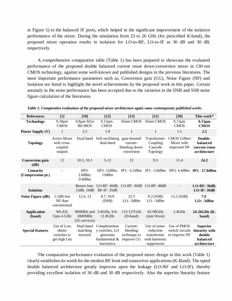
in Figure 5) to the balanced IF ports, which helped in the significant improvement of the isolation
performance of the mixer. During the simulation from 23 to 26 GHz (for prescribed K-band), the
proposed mixer operation results in isolation for LO-to-RF, LO-to-IF as 36 dB and 30 dB,
respectively.
A comprehensive comparative table (Table 1) has been prepared to showcase the evaluated
performance of the proposed double balanced current reuse down-conversion mixer in 130-nm
CMOS technology, against some well-known and published designs in the previous literatures. The
most important performance parameters such as, Conversion gain (CG), Noise Figure (NF) and
Isolation are listed to highlight the novel achievements by the proposed work in this paper. Certain
anomaly in the noise performance has been accepted due to the variation in the DSB and SSB noise
figure calculation of the literatures.
Table 1: Comparative evaluation of the proposed mixer architecture again some contemporary published works
The comparative performance evaluation of the proposed mixer design in this work (Table 1)
clearly establishes its worth for the modern RF front end transceiver applications (K-Band). The opted
double balanced architecture greatly improves upon the leakage (LO-RF and LO-IF), thereby
providing excellent isolation of 36 dB and 30 dB respectively. Also the superior linearity feature
References [1] [10] [12] [15] [21] [30] This work*
Technology 0.18µm
CMOS
0.8µm SiGe
BiCMOS
0.13µm
CMOS
65nm CMOS 65nm CMOS 0.13µm
CMOS 0.13µm
CMOS
Power Supply (V) 1 2.5 1.8 1 1 1.5 2.5
Topology
Active Mixer
with cross-
coupled
outputs
Dual-band Self-oscillating
dual-band
gain-boosted
current-
bleeding down-
conversion
Transformer-
Coupling
Cascode
Topology
CMOS Gilbert
Mixer with
improved NF
Double-
balanced
current reuse
architecture
Conversion gain
(dB)
12 10.5, 10.1 5-12 12 9.5 11.4 24.2
Linearity
(Compression pt.)
- IIP3:
2.6dBm,
0.8dBm
IIP3: 12dBm,
13dBm
IP1: -5.2dBm IP1: -3.8dBm IIP3: 4.4dBm IP1: -17.8dBm
Isolation
- Return loss:
15dB, 10dB
LO-RF: 40dB,
RF-IF: 35dB
LO-RF: 30dB LO-RF: 48dB - LO-RF: 36dB,
LO-IF: 30dB
Noise Figure (dB) 1-2dB less
NF than
conventional
12.6, 13
8.7, 10.9
(DSB)
33.5
LO: -3dBm
9.2 (SSB)
LO: -3dBm
13.2 (SSB) 7.9
LO: -3dBm
Application
(band)
WLAN,
Upto 4 GHz
900MHz and
1800MHz
(2G services)
5-6GHz, 9.8-
11.8GHz
113-127GHz
(D-band)
62-90GHz
(mm Wave)
2.4GHz 24-26GHz (K-
band)
Special features
Use of Low
ohmic
switches to
get high Gm
Dual-band
matching
network
Complementar
y switches, LO
generates
fundamental &
harmonics
Current-
bleeding
technique to
improve CG
Use of noise-
reduction
transformer
with harmonic
suppression
Use of PMOS
switch circuits
to improve NF
Superior
linearity with
double
balanced
architecture

(lower IP1) promises its candidature for the higher dynamic range. This adds on to the higher
conversion gain and makes it hand-picked choice for noisy RF systems, where higher SNR is a
stringent requirement. A reasonable power dissipation (high supply bias for the chosen process node),
has been a soft compromise for the high conversion gain (due to high Gm) and better noise
performance of the mixer’s architecture.
V. CONCLUSION
This paper consists of the qualitative analysis of the modern RF down-conversion mixers and presents
an optimum solution with double balanced current reuse architecture. Various challenges in the RF
receiver architectures and constraints to the conventional mixers’ topologies have been presented and
three major aspects of the multi-band down-conversion mixer architectures, namely high conversion
gain, sub-harmonic dual-band operation and current reuse cross-coupled double-balanced operation
are discussed qualitatively. The proposed design has attempted to incorporate all these aspects and a
double-balanced cross-coupled architecture in 130-nm RF-CMOS (UMC) technology was presented.
High linearity has been achieved as a -17.8 dBm compression point (for 1-dB) with high
transconductance differential pair. The proposed mixer architecture offered the optimum performance
on the above-said aspects of low power, low noise and high conversion gain (24.2 dB). The multi-
band operation capacity has also been verified from the simulation in the ADS environment. With a
2.5 V supply voltage, the mixer consumes an overall dc power of 26.8 mW. These features of higher
conversion gain along with higher compression point and exceptional isolation brings in the novelty
attribute to the presented work. The proposed down-conversion mixer, which employs double-
balanced current reuse cross-coupled architecture has come up with optimized values for all the
essential parameters for an RF CMOS mixer in k-band. This, thereby demonstrates its suitability as
a handpicked model for this RF range applications.
Acknowledgements
We (Authors) would like to thank the Integral Information and Research Centre of Integral
University, Lucknow, India for providing an opportunity to carry out this research work. This work
is an intellectual property of Integral University vides the Manuscript Communication no.
IU/R&D/2019-MCN0001179.
REFERENCES
[1] A. M. Klumperink, S. M. Louwsma, G. J. M. Wienk, and B. Nauta, “A CMOS switched transconductor mixer,'' IEEE J. Solid-State Circuits, vol. 39, no. 8, pp. 1231_1240, Aug. 2004, doi: 10.1109/JSSC.2004.831797.
[2] M. T. Terrovitis and R. G. Meyer, “Noise in current-commutating CMOS mixers,'' IEEE J. Solid-State Circuits, vol. 34,
no. 6, pp. 772_783, Jun. 1999, doi: 10.1109/4.766811.

[3] H. Darabi and A. A. Abidi, “Noise in RF-CMOS mixers: A simple physical model,'' IEEE J. Solid-State Circuits, vol. 35,
no. 1, pp. 15_25, Jan. 2000, doi: 10.1109/4.818916.
[4] B. Guo and G.Wen, “Periodic time-varying noise in current-commutating CMOS mixers,'' Prog. Electromagn. Res., vol.
117, pp. 283_298, 2011, doi: 10.2528/PIER11040706.
[5] W. Cheng, A. J. Annema, J. A. Croon, and B. Nauta, “Noise and nonlinearity modeling of active mixers for fast and
accurate estimation,'' IEEE Trans. Circuits Syst. I, Reg. Papers, vol. 58, no. 2, pp. 276_289, Feb. 2011, doi:
10.1109/TCSI.2010.2072110.
[6] J. Lerdworatawee and W. Namgoong, “Generalized linear periodic time- varying analysis for noise reduction in an active
mixer,'' IEEE J. Solid-State Circuits, vol. 42, no. 6, pp. 1339_1351, Jun. 2007.
[7] B. Bakkaloglu, P. Fontaine, A. N. Mohieldin, S. Peng, S. J. Fang, and F. Dul, “A 1.5-V multi-mode quad-band RF receiver
for GSM/EDGE/CDMA2K in 90-nm digital CMOS process,'' IEEE J. Solid-State Circuits, vol. 41, no. 5, pp. 1149_1159,
May 2006.
[8] V. Jain, F. Tzeng, L. Zhou, and P. Heydari, “A single-chip dual-band 22-29-GHz/77-81-GHz BiCMOS transceiver for
automotive radars,'' IEEE J. Solid-State Circuits, vol. 44, no. 12, pp. 3469_3485, Dec. 2009.
[9] Y.-S. Hwang, S.-S. Yoo, and H.-J. Yoo, “A 2 GHz and 5 GHz dual-band direct conversion RF frontend for multi-standard
applications,'' in Proc. IEEE Int. SOC Conf., Sep. 2005, pp. 189_192.
[10] T. A. Abdelrheem, H. Y. Elhak, and K. M. Sharaf, “A concurrent dual-band mixer for 900-MHz/1.8 GHz RF front-ends,''
in Proc. 46th Midwest Symp. Circuits Syst., vol. 3, Dec. 2003, pp. 1291_1294.
[11] P. de Paco, R. Villarino, G. Junkin, O. Menendez, and E. Corrale, “Dualband mixer using composite right/left-handed
transmission lines,'' IEEE Microw. Wireless Compon. Lett., vol. 17, no. 8, pp. 607_609, Aug. 2007.
[12] B. R. Jackson and C. E. Saavedra, “A dual-band self-oscillating mixer for C-band and X-band applications,'' IEEE Trans.
Microw. Theory Techn., vol. 58, no. 2, pp. 318_323, Feb. 2010.
[13] M. El-Nozahi, A. Amer, E. Sánchez-Sinencio, and K. Entesari, “A millimeter-wave (24/31-GHz) dual-band switchable
harmonic receiver in 0.18-µm SiGe process,'' IEEE Trans. Microw. Theory Techn., vol. 58, no. 11, pp. 2717_2730, Nov.
2010.
[14] A. Mazzanti, M. B. Vahidfar, M. Sosio, and F. Svelto, “A low phase-noise multi-phase LO generator for wideband demodulators based on recon_gurable sub-harmonic mixers,'' IEEE J. Solid-State Circuits, vol. 45, no. 10, pp. 2104_2115,
Oct. 2010.
[15] Chae Jun Lee and Chul Soon Park, “A D-Band Gain-Boosted Current Bleeding Down-Conversion Mixer in 65 nm CMOS
for Chip-to-Chip Communication,” IEEE Microwave and Wireless Components Letters, DOI-
10.1109/LMWC.2016.2517132, 2016.
[16] Y.-H. Chang, C.-Y. Huang, and Y.-C. Chiang, “A 24 GHz down-conversion mixer with low noise and high gain,'' in Proc.
Eur. Microw. Integr. Circuit Conf., Oct. 2012, pp. 285_288.
[17] D. Ahn, D.-W. Kim, and S. Hong, “A K-band high-gain down-conversion mixer in 0.18 µm CMOS technology,'' IEEE
Microw. Wireless Compon. Lett. vol. 19, no. 4, pp. 227_229, Apr. 2009.
[18] Y.-T. Chang, H.-Y. Wu, and H.-C. Lu, “A K-band high-gain downconverter mixer using cross couple pair active load,'' in
Proc. Eur. Microw. Integr. Circuits Conf., Oct. 2016, pp. 377_380.

[19] D.-R. Lin, K.-Y. Kao, and K.-Y. Lin, “A K-band high-gain linear CMOS mixer with current-bleeding neutralization
technique,'' in Proc. IEEE Asia_Paci_c Microw. Conf., Nov. 2018, pp. 267_269.
[20] Yao Peng, Jin He, Haomin Hou, Hao Wang, Sheng Chang, Qijun Huang and Yinxia Zhu, “A K-Band High-Gain and Low-
Noise Folded CMOS Mixer Using Current-Reuse and Cross-Coupled Techniques,” IEEE Access, Digital Object Identifier
10.1109/ACCESS.2019.2941048, VOLUME 7, 2019.
[21] Z. Liu, J. Dong, Z. Chen, Z. Jiang, P. Liu, Y. Wu, C. Zhao, and K. Kang, “A 62-90 GHz high linearity and low noise
CMOS mixer using transformer-coupling cascode topology,'' IEEE Access, vol. 6, pp. 19338_19344, 2018.
[22] B.-J. Huang, K.-Y. Lin, and H. Wang, “Millimeter-wave low power and miniature CMOS multi-cascode low-noise
amplifiers with noise reduction topology,'' IEEE Trans. Microw. Theory Techn., vol. 57, no. 12, pp. 3049_3059, Dec. 2009.
[23] Y.-S. Lin, K.-S. Lan, C.-C. Wang, C.-C. Chi, and S.-S. Lu, “6.3 mW 94 GHz CMOS down-conversion mixer with 11.6
dB gain and 54 dB LO-RF isolation,'' IEEE Microw. Wireless Compon. Lett., vol. 26, no. 8, pp. 604_606, Aug. 2016.
[24] S. G. Lee and J. K. Choi, “Current-reuse bleeding mixer,'' Electron. Lett., vol. 36, no. 8, pp. 696_697, Apr. 2000, doi: 10.1049/el:20000556.
[25] D. Y. Yoon, S.-J. Yun, J. Cartwright, S.-K. Han, and S.-G. Lee, “A high gain low noise mixer with cross-coupled bleeding,''
IEEE Microw. Wireless Compon. Lett., vol. 21, no. 10, pp. 568_570, Oct. 2011, doi: 10.1109/LMWC.2011.2166251.
[26] Deepak Balodi, Dr. Arunima and Prof. P.A. Govindacharyulu, “Low power LC-voltage controlled oscillator with -140
dBc/Hz @ 1 MHz offset using on-chip inductor design in 0.13 mm RF-CMOS process for S-Band application”, Circuit
World (EMERALD Publishing Limited), ISSN 0305-6120, DOI 10.1108/CW-03-2019-0023, Nov-2019.
[27] Deepak Balodi, Dr. Arunima and Prof. P.A. Govindacharyulu, “Ultra-Wideband Quadrature LC-VCO using Capacitor-
Bank and Backgate Topology with On-Chip Spirally Stacked Inductor in 0.13 μm RF-CMOS Process Covering S-C
Bands,” Microelectronics Journal (ELSEVIESR), MEJ_104727, ISSN 0026-2692, DOI: 10.1016/j.mejo.2020.104727,
Mar-2020.
[28] H. Darabi and J. Chiu, ``A noise cancellation technique in active RF-CMOS mixers,'' IEEE J. Solid-State Circuits, vol. 40,
no. 12, pp. 2628_2632, Dec. 2005, doi: 10.1109/JSSC.2005.857428.
[29] J. Park, C.-H. Lee, B.-S. Kim, and J. Laskar, “Design and analysis of low flicker-noise CMOS mixers for direct-conversion
receivers,'' IEEE Trans. Microw. Theory Techn., vol. 54, no. 12, pp. 4372_4380, Dec. 2006, doi: 10.1109/TMTT.2006.885582.
[30] J. Yoon, H. Kim, C. Park, J. Yang, H. Song, S. Lee, and B. Kim, “A new RF CMOS Gilbert mixer with improved noise
figure and linearity,'' IEEE Trans. Microw. Theory Techn., vol. 56, no. 3, pp. 626_631, Mar. 2008, doi:
10.1109/TMTT.2008.916942.