a microstrip-coupled slot-loop antenna for integrated receivers in the millimeter-wave band
TRANSCRIPT

A MICROSTRIP-COUPLED SLOT-LOOPANTENNA FOR INTEGRATEDRECEIVERS IN THEMILLIMETER-WAVE BAND
1 ´ 1Pablo Otero, Alejandro Alvarez-Melcon,´Jean-Francois Zurcher,1 and Juan R. Mosig1¨1 ´ ( )Laboratoire d’Electromagnetisme et d’Acoustique LEMA´´ ( )Ecole Polytechnique Federale de Lausanne EPFL´ ´CH-1015 Lausanne, Switzerland
Recei ed 3 December 1997
ABSTRACT: A square-loop slot antenna, printed at the back surfaceof an extended hemispherical lens, is examined as a candidate for
( )millimeter-wa e mm-wa¨e integrated-circuit Schottky-diode mixers. Theloop slot is etched in a microwa e substrate, and coupled to a microstripline section printed on the other side of the substrate. A Schottky barrierdiode shunted to ground is the mixing de¨ice. The input impedance ofthe antenna has been optimized to conjugate match the Schottky diode.To design and optimize the antenna, an efficient full-wa¨e method of
( )moments MoM technique, which sol es the mixed potential integral( )equation MPIE in the stratified medium, has been de¨eloped. Patterns
ha¨e been computed using the physical optics approximation anddiffraction theory. The proposed configuration shows ¨ery widebandperformance. Simulation results compare well with measurements. Theproposed configuration is suitable to be scaled down for operation in the
( )submillimeter-wa e submm-wa e band. Q 1998 John Wiley & Sons,Inc. Microwave Opt Technol Lett 18: 91]95, 1998.
( )Key words: mixed potential integral equation MPIE ; method of( )moments MoM ; planar antennas; slot antennas; millimeter wa¨e
1. INTRODUCTION
An increased interest in planar integrated receivers for themm- and submm-wave bands has been observed recently. Themain reason is the desire to replace the waveguide-basedtechnology currently used in spaceborne applications. In thiscontext, previous work has shown the feasibility of using
Žuniplanar technology coplanar transmission-line-fed slot an-.tennas , coupled to extended hemispherical dielectric lenses,
w xand integrating a mixing device 1 . This design is sought tooperate as a front-end feed for reflector-type antennas. How-ever, when scaled to the submm-wave band, the location ofthe mixing device, a Schottky barrier diode, integrated withthe coplanar waveguide, results in an asymmetric configura-
w xtion with too high sidelobe levels 2 . To ensure the symmetryand to isolate the diode from the radiation semispace, anantenna configuration, already used in the 1980s in C- and
w xX-bands, has been tried 3 . Figure 1, where all units aremillimeters, shows the proposed design. The Schottky diode isonly symbolically represented, as well as the intermediate
Ž .frequency IF filter and the extended hemispherical lens.The IF filter is a nine-section, quarter-wavelength trans-former, low-pass filter with a cutoff frequency of about40 GHz. The low relative permittivity substrate is mountedon the plane surface of the dielectric lens. The radius of thelens is much larger than the one shown in Figure 1. Theutilized substrate is RTrDuroid 5870, e s 2.33, tan d sr
w x0.0012, and h s 0.254 mm 4 . The face which is in contactwith the lens has a conductor plane where a square slot loophas been etched. On the other substrate’s face, a microstripline section couples to the slot loop at one end and feeds themixing diode at the other. The IF signal is extracted from thesame diode terminal, as shown in Figure 1. For our experi-
Ž .ments, the local oscillator LO signal has been injectedthrough the same filter, so that subharmonic mixing has beenperformed. For a possible scaled prototype operating atsubmm-wave frequencies, quasioptical LO signal injectioncan also be used.
The two main problems of the original design, when suchhigh frequencies are used, are the appearance of surfacewaves and the too high losses in microstrip lines. The formeris controlled by an appropriate choice of the substrate thick-
w xness and permittivity. As shown by Gupta et al. 5 , the cutofffrequency f of the first higher order mode in a microstripcline is given approximately by
300Ž .f , 1c Ž .e 2W q 0.8h' r
where f is in gigahertz, e is the substrate relative permittiv-c rity, W is the microstrip width in millimeters, and h is thesubstrate thickness, also in millimeters. For the RTrDuroid5870 substrate used in the present design, to have f - f ,op cwhere f is the operating frequency, we needop
98Ž . Ž .W mm - y 0.1. 2Ž .f GHzop
The widths of the designed microstrip lines satisfy this condi-Ž .tion. Equation 1 shows that the smaller e and h are, ther
less power conveyed into surface waves. This is a designadvantage because the larger the effective relative permittiv-ity ratio at both sides of the slot loop plane, the larger the
w xfront-to-back power ratio of the antenna 6 .The second problem of the design is due to the high
ohmic losses of microstrip lines at mm- and submm-wavefrequencies. The present solution uses the shortest possiblelength of microstrip at these frequencies, as can be seen inFigure 1. Beyond the diode, only the IF signal propagates. Avery important feature of the design is that the slot loopperimeter and the microstrip length are quite independent.This fact has two main advantages: first, diode matching canbe carried out with little concern about the slot loop size and,second, the frequency band can be widened compared to
w xprevious uniplanar designs 7 . Indeed, it is possible that theantenna itself conjugate matches the diode. This techniquehas already been used with success in the previously men-tioned designs. The sought input impedance of the antenna istherefore not 50 V, but rather ZU . A typical Schottkydiode
Ž .diode impedance at 65 GHz, Z s 50 y j50 V, has beendiodeused.
2. ANALYTIC METHODS
2.1. Theoretical Model. For the analysis of the radiatingstructure proposed, a standard integral equation formulatedin the space domain has been derived. In the slot interfaces,Love’s equivalence principle is used, and suitable magneticcurrents are defined to help impose the continuity conditionsfor the transverse electric and magnetic fields. The self-inter-
Ž .actions electric]electric and magnetic]magnetic are solvedwith the aid of the vector and scalar potential Green’s func-tions, especially well suited due to their weak singular behav-
w xiors when the source]observer distance r vanishes 8 . Allother interactions, nonexhibiting singularities, are treateddirectly using the electric and magnetic field Green’s func-
MICROWAVE AND OPTICAL TECHNOLOGY LETTERS / Vol. 18, No. 2, June 5 1998 91

Figure 1 Proposed design. All units in millimeters
tions, thus leading to a very compact analytical treatment ofthe problem.
Multilayered media potential and field Green’s functionsare first obtained in the spectral domain using the transverseequivalent transmission line network representation of thestructure along the stratified axis. Following this formalism,the spectral-domain Green’s functions associated to electricand magnetic dipoles are easily obtained by computing equiv-alent voltages and currents in the resulting transmission line
w xnetworks 9 . Once the spectral-domain Green’s functions arecomputed, their spatial-domain counterparts can be obtainedthrough the well-known Sommerfeld integral, and the effi-
w xcient numerical techniques described in 8 have been used.After efficient evaluation of the space-domain Green’s func-tions, the imposition of the boundary conditions for the fieldsin the specific structure shown in Figure 1 yields the followingvector coupled system of integral equations on the unknown
Ž . Ž .induced electric J and magnetic M currents:s s
1Že.E s jv G ? J dS9 y =G =9 ? J dS9HH HHA s V sjvS Se e
Ž .y G ? M dS9 3HH EM sSm
0 s jv G q G ? M dS9HH Fu Fl sž /Sm
1Ž .y = G q G =9 ? M dS9HH Wu W l sjv Sm
Ž .y G ? J dS9 4HH HJ sSe
Že.where E is the exciting or impressed field due to thegenerator applied to the strip line, S is the surface ofethe strip line, and S is the surface of the slot loop. Themsubscripts u and l of Green’s functions stand for above andbelow, respectively, the conductor plane where the slots areetched.
2.2. Numerical Methods. For the solution of the vector-cou-pled system of integral equations previously derived, a Ga-
Ž .lerkin method of moments MoM algorithm based on sub-sectional rooftop functions has been developed. The maindifficulty in the implementation of the proposed approach isthe efficient numerical evaluation of the fourfold overlappingintegrals between the spatial-domain Green’s functions andthe rooftop basis and test functions. In the present work, thecross-correlation integrals of the rooftop functions have beenused together with the symmetry properties of Green’s func-tions to systematically reduce all fourfold integrals into dou-ble integrals, thus considerably reducing the computationaleffort. For the singular cases, a further transformation to thepolar plane is performed in order to analytically extract theŽ .1rr singular behavior of the potential Green’s functions.Thanks to the analytical extraction procedure applied, theremainder function behaves very smoothly, and standard nu-merical integration techniques can be applied, obtaining goodaccuracy with a limited number of integration points. InFigure 2, we present the value obtained for a typical singularMoM element as a function of the number of integrationpoints. The computation is performed for the structure shownin Figure 1 and for the frequency of 70 GHz. We can observe
Ž .that good convergence is obtained with only 4 = 4 integra-tion points, the relative error being smaller than 0.1%.
The developed software tool takes only 4 s per frequencypoint on an HP712r80 platform to complete the analysis ofthe antenna structure shown in Figure 1, when only one cellis used in the transverse direction of the strip line and loop.Even when, looking for increased accuracy, the discretizationis performed with three cells in the transverse direction, thesoftware still only takes 18 s per frequency point on the sameplatform. These results clearly indicate that the developedsoftware can be used as a real tool for the efficient optimiza-tion of this type of antennas.
2.3. Lens Analysis. The field in the far region from the lensmay be calculated by means of the Love’s equivalence princi-ple, which allows substitution of the lens by a perfect conduc-
MICROWAVE AND OPTICAL TECHNOLOGY LETTERS / Vol. 18, No. 2, June 5 199892

Figure 2 Relative and absolute values of a typical singular MoM element as a function of the number of integration points.Numerical test is performed for the structure shown in Figure 1 and at a frequency of 70 GHz
tor and equivalent electric and magnetic surface currents.Physical optics approximation, based on image theory, allowsthe electric current to be considered as short circuited. Theequivalent magnetic surface current is proportional to theelectric field on the outer surface of the lens. This field iscomputed accepting that the lens radius is much larger thanthe wavelength in the lens dielectric, so that Fresnel’s trans-mission coefficients may be used.
3. RESULTS
All simulated and measured results shown below correspondto the integrated antennarmixer depicted in Figure 1. Fig-ure 3 shows the module of the generalized load reflection
w xcoefficient, as defined by Collin 11 , in decibels, that is,
UZ y Zdiode ant Ž .G s 20 log . 5L Z q Zdiode ant
Simulations presented in Figure 3 correspond to two differentmeshing resolutions. The solid line is obtained when slot andstrip widths contain a single cell. To obtain the dotted line,width is divided into three cells. No significant changes areobtained when further increasing the number of transversecells, which verifies the convergence of the numerical method.In addition, Figure 3 shows the onset of a double-resonancephenomenon, expected from the discussion in Section 1. Oneresonance is related to the slot loop size, and the other one isdetermined by the coupling microstrip section length. Band-width is then larger than in uniplanar designs. For a reflec-tion coefficient of y10 dB, the bandwidth is about 20%,
w xwhich is better than previous designs 7 .Figures 4 and 5 show the simulated and measured radia-
tion patterns in the E- and H-planes, respectively, at 65 GHz.Figure 6 shows the E-plane pattern at 70 GHz. The H-planepattern barely changes with frequency, and therefore it isnot shown. All of these patterns are for an extension lengthof L s 8.5 mm, which is between the hyperhemisphereextŽ . ŽL s 7.2 mm and the synthesized ellipsoid L ,ext ext
.9.6 mm . Measured patterns show reasonable agreement with
Figure 3 Generalized load reflection coefficient between antennaand diode versus frequency for two different grids
the simulated patterns. Moreover, the H-plane pattern showsan extremely low sidelobe level, and it changes very little withfrequency. The E-plane sidelobe level is not as good as the
w xH-plane one. However, it is better than previous designs 2and improves with frequency, as can be observed in Figure 6.Even though the loop is perfectly symmetric, the equivalentmagnetic currents that the microstrip creates in the slot arenot uniformly distributed on both sides of the loop becausefeeding is done only on one side. This fact is considered byour in-house simulation tools, but the predicted asymmetry isnoticeably smaller than the measured one, as observed on theleft sidelobe of the patterns in Figure 4. The left sidelobe istherefore probably due to uncontrolled spurious propagationphenomena generated by the diode.
Predictions for directivity of the lens antenna at 65 GHzversus extension length are shown in Figure 7. An inflection
MICROWAVE AND OPTICAL TECHNOLOGY LETTERS / Vol. 18, No. 2, June 5 1998 93

Figure 4 Simulated and measured E-plane patterns at 65 GHzwith L s 8.5 mmext
Figure 5 Simulated and measured H-plane patterns at 65 GHzwith L s 8.5 mmext
point is observed at the hyperhemispherical position. Themaximum directivity is obtained close to the synthesizedellipsoidal point, as expected. The lens antenna directivity, aswell as the input impedance previously shown, cannot bedirectly measured, so far, at our laboratory. Instead, the
Ž . w xisotropic conversion gain ICG 12 has been measured,which is shown in Figure 8. The ICG is defined as the powerdelivered to the IF load from a copolarized incident planewave by an antenna mixer or an antenna amplifier]mixer,divided by the power that would have been received by anisotropic antenna with a matched load. The ICG is a magni-tude that groups antenna and mixer parameters such as the
Ž .antenna gain directivity and losses , the antennarmixingdevice mismatch, the mixer conversion loss, and the IF filterinsertion loss. The ICG is a figure of merit of a frequencyconverter which may be used when the mentioned parame-
Figure 6 Simulated and measured E-plane patterns at 70 GHzwith L s 8.5 mmext
Figure 7 Simulated lens antenna directivity versus extension lengthat 65 GHz
ters cannot be directly measured. In our prototype, the ICGperformance is similar to that obtained in previous designs,and good agreement is obtained with predicted bandwidth inFigure 3.
4. CONCLUSIONS
A type of square-loop slot antenna, coupled to a microstripline section, has been examined as a candidate for a milli-meter-wave integrated-circuit Schottky-diode mixer. Theantenna has been optimized to match the typical inputimpedance of such diodes in the millimeter-wave band. Opti-mization has been performed by means of an efficient MoManalysis software tool specifically developed for this study.The antenna shows a very wide frequency band, clean androtationally symmetric patterns, and a good compromise be-
MICROWAVE AND OPTICAL TECHNOLOGY LETTERS / Vol. 18, No. 2, June 5 199894
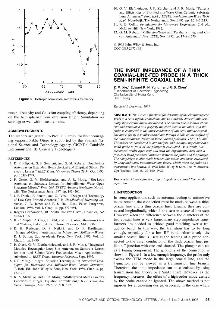
Figure 8 Isotropic conversion gain versus frequency
tween directivity and Gaussian coupling efficiency, dependingon the hemispherical lens extension length. Simulation re-sults agree well with measurements.
ACKNOWLEDGMENTS
The authors are grateful to Prof. F. Gardiol for his encourag-ing support. Pablo Otero is supported by the Spanish Na-
Žtional Science and Technology Agency, CICYT ‘‘Comision´.Interministerial de Ciencia y Tecnologıa’’ .´
REFERENCES
1. D. F. Filipovic, S. S. Gearhart, and G. M. Rebeiz, ‘‘Double-SlotAntennas on Extended Hemispherical and Elliptical Silicon Di-electric Lenses,’’ IEEE Trans. Microwa e Theory Tech., Oct. 1993,pp. 1738]1749.
2. P. Otero, G. V. Eleftheriades, and J. R. Mosig, ‘‘Slot-LoopAntennas on Substrate Lenses for Submillimeter-Wave OpenStructure Mixers,’’ Proc. 20th ESTEC Antenna Workshop, Noord-wijk, The Netherlands, June 1997, pp. 193]200.
3. J. P. Daniel, E. Penard, and C. Terret, ‘‘Design and Technologyof Low-Cost Printed Antennas,’’ in Handbook of Microstrip An-tennas, J. R. James and P. S. Hall, Eds., Peter Peregrinus,London, 1989, Vol. 1, Chap. 11, pp. 579]691.
4. Rogers Corporation, 100 South Roosevelt Ave., Chandler, AZ85226 USA.
5. K. C. Gupta, R. Garg, I. Bahl, and P. Bhartia, Microstrip Linesand Slotlines, 2nd ed., Artech House, Norwood, MA, 1996.
6. D. B. Rutledge, D. P. Neikirk, and D. P. Kasilingam,‘‘Integrated-Circuit Antennas,’’ in Infrared and Millimeter Wa¨es,K. J. Button, Ed., Academic Press, New York, 1983, Vol. 10,Chap. 1, pp. 1]90.
7. P. Otero, G. V. Eleftheriadesand, and J. R. Mosig, ‘‘IntegratedModified Rectangular Loop Slot Antenna on Substrate Lensesfor mm- and Submm-Wave Frequencies Mixer Applications,’’submitted to IEEE Trans. Antennas Propagat., Sept. 1997.
8. J. R. Mosig, ‘‘Integral Equation Technique,’’ in Numerical Tech-niques for Microwa e and Millimeter-Wa e Passi e Structures,T. Itoh, Ed., John Wiley & Sons, New York, 1989, Chap. 3, pp.133]213.
9. K. A. Michalski and J. R. Mosig, ‘‘Multilayered Media Green’sFunctions in Integral Equation Formulations,’’ IEEE Trans. An-tennas Propagat., Mar. 1997, pp. 508]519.
10. G. V. Eleftheriades, J. F. Zurcher, and J. R. Mosig, ‘‘Patterns¨and Efficiencies of Slot-Fed mm-Wave Glass-Ceramic SubstrateLens Antennas,’’ Proc. ESA r ESTEC Workshop mm-Wa e Tech.Appl., Noordwijk, The Netherlands, Nov. 1995, pp. 2.2.1]2.2.13.
11. R. E. Collin, Foundations for Microwa e Engineering, 2nd ed.,McGraw-Hill, New York, 1992.
12. G. M. Rebeiz, ‘‘Millimeter-Wave and Terahertz Integrated Cir-cuit Antennas,’’ Proc. IEEE, Nov. 1992, pp. 1748]1770.
Q 1998 John Wiley & Sons, Inc.CCC 0895-2477r98
THE INPUT IMPEDANCE OF A THINCOAXIAL-LINE-FED PROBE IN A THICKSEMI-INFINITE COAXIAL LINEZ. M. Xie,1 Edward K. N. Yung,1 and R. S. Chen11 Department of Electronic EngineeringCity University of Hong KongHong Kong
Recei ed 5 December 1997
ABSTRACT: The Green’s functions for determining the electromagneticfields in a semi-infinite coaxial line due to a radially directed infinitesi-mally short electric dipole are deri ed. The coaxial line is shorted at oneend and terminated at a perfectly matched load at the other, and theprobe is connected to the inner conductor of this semi-infinite coaxialline and is fed by a smaller coaxial line through a hole on the surface ofthe outer conductor. Based on these Green’s functions, TEM, TE, andTM modes are considered in our analysis, and the input impedance of asmall probe in front of the plunger is calculated. As a result, ourtheoretical results agree ¨ery well with the experimental data o¨er afrequency band for se¨eral distances between the probe and the plunger.The comparison is also made between our results and those calculatedby using traditional transmission line theory, which treats the probe as atransmission line branch. Q 1998 John Wiley & Sons, Inc. MicrowaveOpt Technol Lett 18: 95]100, 1998.
Key words: Green’s function; input impedance; coaxial line; modeexpansion
I. INTRODUCTION
In some applications such as antenna feeding or microwavemeasurement, the connection must be made between a thickcoaxial line and a thin coaxial line. Usually, they are con-nected longitudinally, which is the case in a coaxial line step.However, when the difference between the diameters of thetwo coaxial lines is very large, many step impedance trans-formers are needed to achieve good matching over a fre-quency band. In this way, the transition has to be longenough, especially for a low RF band. Alternatively, thesmaller coaxial line is used as the feeding of a probe con-nected to the inner conductor of the thick coaxial line, justlike a T-junction with one end shorted. The plunger can actas a tuning component. The geometry of the connection isshown in Figure 1. In a low enough frequency, the probe onlyexcites the TEM mode in the large coaxial line, and theT-junction can be viewed as a transmission line branch.Therefore, the input impedance can be calculated by usingtransmission line theory or a Smith chart. However, as thefrequency increases, the effect of a high-order mode excitedby the probe cannot be ignored. The above method is notrigorous for engineering design, especially in the case where
MICROWAVE AND OPTICAL TECHNOLOGY LETTERS / Vol. 18, No. 2, June 5 1998 95