a multiphysics approach to magnetron and microwave oven design … · 2020-03-02 · a multiphysics...
TRANSCRIPT
WHITEPAPER
A MULTIPHYSICS APPROACH TO MAGNETRON AND MICROWAVE OVEN DESIGN
The magnetrons used in microwave ovens operate on the same frequency band as Wi-Fi equipment, and the radiation they release can interfere with the operation of wireless networks. This paper presents a multiphysics simulation of a magnetron using CST Studio Suite®[1], with the aim of testing the electrical, magnetic, thermal and mechanical characteristics of a low-interference magnetron design. The simulation results are then compared to measurements made experimentally, and the two sets of results are shown to be in good agreement.
Magnetrons are widely used as RF power sources because they offer high energy conversion efficiency (around 75%) at a low cost. The magnetron was invented during World War II, when its small size, high power and short wavelength made it ideal for use in radar, but with mass production and the development of automatic manufac-turing techniques, magnetrons made the move into the home as the radiation source in microwave ovens.
The problem with the microwave oven’s widespread adoption is that magnetrons generate significant amounts of RF noise; the ones used in ovens radiate at around 2.45 GHz. Historically this frequency band was reserved for noisy industrial applications, and little consideration was given to the risk of electromagnetic interference (EMI), but the rise of short-range wireless communication sys-tems such as Wi-Fi and Bluetooth operating on the same frequencies means the microwave oven is now a major potential source of interference to computer networks and mobile communications.
The risk of interference has forced researchers and engi-neers to look for ways to improve the EMI profile of the ovens. There have already been a number of innovations made in magnetron design meant to reduce interference. For instance, magnetrons can be designed with inhomo-geneous magnetic fields to inhibit the production of stray modes, and the cathode heaters can be designed to switch off when not needed, so currents in the filament do not interact with the fields and change the resonant frequency of the magnetron. These approaches both result in a cleaner EM spectrum.
However, although these approaches are good at reduc-ing the sideband noise caused by unwanted resonances in the magnetron, they can’t do much about the radiation that the magnetron produces at its intended mode. Since we can’t get rid of this noise, the only way to stop it interfering with Wi-Fi is to change the magnetron’s reso-nant frequency.

Although magnetrons are restricted to the same frequency band as Wi-Fi, the way the Wi-Fi spectrum is divided up into channels means that there is still room to reduce the risk of interference, by shifting the magnetron’s resonant frequen-cy away from the middle of the spectrum towards the outer edges, as shown in Figure 1. This opens up more channels and increases the chances that the network equipment can find a free channel to communicate on.
However, changing the resonant frequency of a magnetron means changing its electrical properties significantly, and in testing it’s important to be aware of how these changes can affect its magnetic, mechanical, thermal and farfield proper-ties.
There are a number of components that an oven magnetron needs to generate microwaves, illustrated in Figure 2:
• A heated filament cathode, which acts as the electron source.
• An anode with multiple resonant cavities, separated by metal vanes. The walls of these cavities form simple LC circuits.
• Metal rings, known as straps, which connect alternate vanes and ensure they remain in phase, suppressing unwanted modes.
• A pair of permanent ceramic ring magnets – one above the anode and one below – to steer the electrons around the cathode.
• Iron pole pieces between the magnets and the anode to focus the magnetic field.
• An antenna through which the microwaves are transmit-ted.
As well as these, simulations also have to take into account the structural elements of the magnetron. The magnetron is held together by a yoke – a metal frame around the magne-tron – with a heat sink between the anode and the yoke. All of these parts will have to be adjusted or tested during these simulations.
Their properties can all be tested in the lab with prototypes. However, producing a prototype is time consuming and expensive, and finding and fixing a fault means redesigning and rebuilding the prototype. Modeling offers a way of shortening the design cycle by reducing the number of pro-totyping stages needed. The properties of the magnetron can be simulated on the computer and faults identified before the first prototype is built.
FINDING THE COLD RESONANT FREQUENCY WITH THE EIGENMODE SOLVER
The first step of the process is to change the magnetron’s resonant frequency. Magnetrons generate microwaves from the oscillations of fields in the anode’s cavities, driven by the rotation of a wheel of electrons. Inside the magnetron, elec-
Figure 1: Channels in the 2.4 GHz Wi-Fi spectrum. Shifting the microwave oven to a higher operating frequency reduces the number of channels it can interfere with.
Figure 3: The eigenmode of the magnetron.
Figure 2: The structure of a typical magnetron in cross-section.1. Top permanent ceramic ring magnet2. Top pole piece3. Bottom pole piece4. Bottom permanent ceramic ring magnet5. Antenna6. 10 vane resonant cavity7. Yoke8. Heat sink finsAntenna cap, heated fi lament cathode, filament insulator and harmonic choke are not shown.
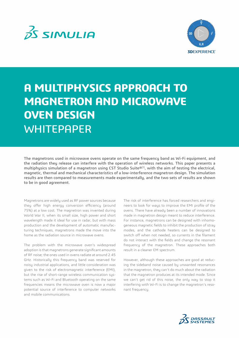
trons tend to spiral out from the cathode to the anode. However, because the vanes of the anode form resonant circuits, the potential distribution over the anode is not con-stant.
Like most magnetrons, ours operates at the π-mode, so there is a 180° phase shift between pairs of adjacent vanes – in other words, because alternate vanes are strapped together, each one has the opposite polarity to its neighbors. The moving field in the magnetron at π-mode accelerates electrons in some parts of the chamber and decelerates those in other parts. Since the anode has 10 vanes, this pro-duces an electron beam with five spokes. As the LC circuits oscillate, the potentials swap sides and the electron beam is rotated – this rotation in turn pumps more energy into the circuits and sustains the oscillations.
Changing the resonant frequency is a matter of changing the behavior of these LC circuits by altering the geometry of the anode. In this case, we adjusted its capacitance by changing the gap between the anode and its straps. Parameterizing this gap is a simple way of fi nding the geometry that will give us the resonant frequency we need. The eigenmode solver of CST Studio Suite provides fast calculations of the magnetron’s cold resonant frequency; for the model used in this example, which had 94,329 tetrahedral mesh cells, the eigenmode solver took 6 minutes and 6 seconds to calculate its resonant frequency on workstation with dual 2.4 GHz Intel Xeon E5645 processors and 128 GB RAM. With the eigenmode solver, we can quickly run an optimizer or per-form a parameter sweep over a range of different values for the strap gap to find a magnetron with the right resonant frequency.
However, the cold resonant frequency is only an approxima-tion of the resonance when the magnetron is actually in use. When the electron beam inside the magnetron interacts with the electromagnetic fields, it disturbs them, and this changes the resonances of the cavities. For an accurate simulation of the magnetron when it’s in use, we need to be able to model the electron beam itself.
MODELING THE FIELDS IN CST EM STUDIO
Before we inject the particles, we need to set up the fields that will steer them. To study the fields inside the magne-tron, we use the electrostatic field solver and the magneto-static field solver, in CST Studio Suite.
The permanent magnets ensure that the particles orbit cor-rectly around the central cathode, so it is important to make sure the magnetic fields behave as expected inside the mag-netron. These fields are not trivial: to make sure the mag-netic fields are focused in the interaction region between the anode and cathode, there are two hollow truncated cones of iron between the magnets and the electrodes. These are the pole pieces, and they act as ferromagnets in the presence of the permanent magnets. These focus the field, so that it is
Figure 4: The magnetic field within the magnetron. The magnets, pole pieces, yoke and interaction region together form a magnetic circuit.
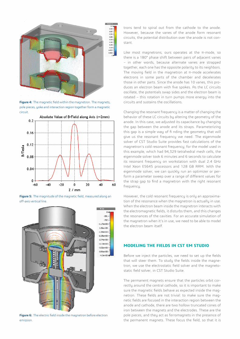
Figure 5: The magnitude of the magnetic field, measured along an off-axis vertical line.
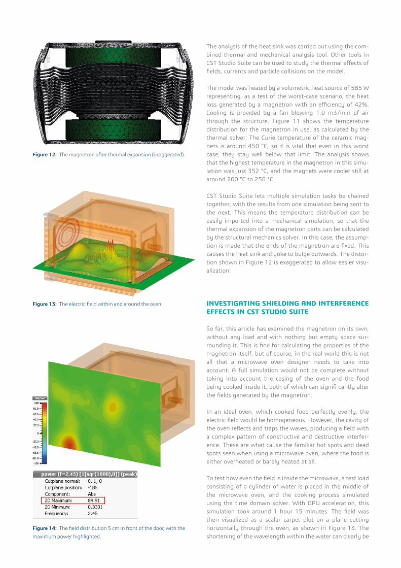
Figure 6: The electric field inside the magnetron before electron emission.

Figure 7: The spoked particle beam. Vanes alternately attract and repel electrons.
Figure 8: The set-up of the ports and monitors.
strong and fairly homogeneous in the area between the anode and cathode.
The magnetostatic field solver is capable of taking the non-linear properties of the materials into account. This makes it ideal for simulating the iron pole pieces, whose ferromagne-tism varies strongly with the field around it.
Figure 4 shows a vector plot of the magnetic field inside the magnetron, and Figure 5 shows the magnitude of the field along a line parallel to the axis (r = 2 mm). Only the magnets, pole pieces and yoke have been included in the simulation – the electrodes and the casing could have been included, but they have little effect on the magnetic fi eld and would have extended the simulation time.
The B-field maximum from the simulation agrees well with the design value of 0.19 T. The largest peak corresponds to the field in the interaction region, while the smaller peaks are the fields within the inner radius of the magnets. As shown in the 3D model, the fields are localized almost entirely to the area between the pole pieces. The magnetic current returns through the yoke, and there is virtually no B-field outside it – the yoke makes a good shield.
While the magnetic field gives the particles angular motion, the electric field gives them radial motion. Together, the magnetic and electric fields define the drift velocity of the particles. The drift velocity must be synchronous to the phase velocity of the operating mode, so the electrons orbit the cathode at the right speed to generate resonances in the cavities.
Figure 6 shows a scalar isoline plot of the electric potential distribution between anode and cathode. The field varies evenly in the interaction region.
This field is purely electrostatic, induced by the potential applied to the electrodes. The simulation does not take into account the variations in the field induced by oscillations in the LC circuits, which cause the electron beam to develop spokes. A full dynamic simulation will need to be able to simulate the time-dependent electric field that generates the microwaves, and that is where the particle simulation comes in.
SIMULATING THE ELECTRON BEAM WITH THE PIC SOLVER
To study the electron beam, we use the particle solvers in CST Studio Suite. Since a microwave oven magnetron is not a relativistic device, we can simulate the behavior of the elec-trons best using the Child-Langmuir space charge model, with a space charge limited current of 20 A. The cathode is designated as a particle source, spraying electrons through-out the magnetron chamber. The particle-in-cell solver (PIC) available in CST Studio Suite then lets us model this electron cloud as it forms a coherent beam. An example of a particle beam in the π-mode is shown in Figure 7.
Moving charges induce electric and magnetic fi elds, and these fields affect the paths of the moving charges. The PIC solver takes into account the coupling between the electrons and the field, simulating the motion of the particles and the field around them in the time domain. Because it can model particles over their whole path, the PIC solver gives us the fi elds over an extended period of time, rather than just at one instant. With it we can examine the beam loading effect – the interaction between the particle beam and the fields within the magnetron which alters its resonant frequency.
The PIC solver can take advantage of GPU computing to speed up the simulation process substantially. When the particle beam inside the magnetron was simulated, with a

Figure 9: The output of the magnetron over time. The magnetron takes around 50 nanoseconds to start resonating.
Figure 10: The frequency spectrum of the magnetron in linear scaling.
Figure 11: The temperature distribution across the magnetron.
2,567,708 mesh cell model and an average of 1.22 million electrons in the beam, it took 6 hours and 15 minutes to run on a computer with dual 2.4 GHz Intel Xeon E5620 proces-sors, 48 GB RAM and a Tesla C2050 GPU. With GPU com-puting disabled, the same computer took 32 hours and 48 minutes to carry out the simulation, more than 5 times lon-ger. This speed-up scales almost linearly with the number of particles – the more particles in the simulation, the more useful GPU computing is. From the signals generated by the PIC Solver, we can calculate a number of the magnetron’s properties. Most importantly, it gives us the true resonant frequency of the magnetron. The ends of the magnetron can be designated as waveguide ports, and the solver will calcu-late the modes at these ports, along with the line impedance between them. The time signal at the output port corre-sponds to the power of the magnetron. We can also turn the time signal into a spectrum in the frequency domain by using a Fourier transform.
Current and voltage monitors can also be defi ned with the PIC Solver. These can give us the power drawn by the cath-ode which, when combined with the output power of the magnetron, lets us calculate its efficiency. The port and monitor definitions for this model are shown in Figure 8 – the red rectangles are the waveguide ports and the lines marked with circles are the monitors.
As shown in Figure 9, for the first 40 nanoseconds of opera-tion, the magnetron produces little power. This is because the particle beam has not formed spokes, so the oscillations are not yet coherent. After this time, its output grows rap-idly, and once it is resonating it produces a clean, constant signal. This signal effectively represents the square root of the output power – in other words, the rms output power is half the square of the peak signal. The calculated output power of the magnetron is 1095.12 W (half of 46.82), close to its rated value of 1000 W, and taking the Fourier trans-form of the time signals, as shown in Figure 10, gives us the hot resonant frequency, 2.471 GHz. For comparison, this particular magnetron had a cold resonant frequency of 2.49 GHz – the 20 MHz difference is due to this beam loading effect.
THERMAL AND MECHANICAL ANALYSIS
Once the magnetron itself has been tested, the next step of the design process is to test the heat sinks. The inductive and capacitive components of the magnetron give it a significant impedance; in a typical magnetron, 30% to 50% of the input energy is lost as heat. Magnetrons are quite sensitive to heating, because of the ceramic magnets used to steer the beam. If these magnets are heated past their Curie tempera-ture, they will lose their magnetism, and the magnetron will no longer be able to generate the wheel of electrons needed to maintain stable oscillations. To prevent this happening, the heat needs to be carried away efficiently.
The analysis of the heat sink was carried out using the com-bined thermal and mechanical analysis tool. Other tools in CST Studio Suite can be used to study the thermal effects of fields, currents and particle collisions on the model.
The model was heated by a volumetric heat source of 585 W representing, as a test of the worst-case scenario, the heat loss generated by a magnetron with an efficiency of 42%. Cooling is provided by a fan blowing 1.0 m3/min of air through the structure. Figure 11 shows the temperature distribution for the magnetron in use, as calculated by the thermal solver. The Curie temperature of the ceramic mag-nets is around 450 °C, so it is vital that even in this worst case, they stay well below that limit. The analysis shows that the highest temperature in the magnetron in this simu-lation was just 352 °C, and the magnets were cooler still at around 200 °C to 250 °C.
CST Studio Suite lets multiple simulation tasks be chained together, with the results from one simulation being sent to the next. This means the temperature distribution can be easily imported into a mechanical simulation, so that the thermal expansion of the magnetron parts can be calculated by the structural mechanics solver. In this case, the assump-tion is made that the ends of the magnetron are fixed. This causes the heat sink and yoke to bulge outwards. The distor-tion shown in Figure 12 is exaggerated to allow easier visu-alization.
INVESTIGATING SHIELDING AND INTERFERENCE EFFECTS IN CST STUDIO SUITE
So far, this article has examined the magnetron on its own, without any load and with nothing but empty space sur-rounding it. This is fine for calculating the properties of the magnetron itself, but of course, in the real world this is not all that a microwave oven designer needs to take into account. A full simulation would not be complete without taking into account the casing of the oven and the food being cooked inside it, both of which can signifi cantly alter the fields generated by the magnetron.
In an ideal oven, which cooked food perfectly evenly, the electric field would be homogeneous. However, the cavity of the oven reflects and traps the waves, producing a field with a complex pattern of constructive and destructive interfer-ence. These are what cause the familiar hot spots and dead spots seen when using a microwave oven, where the food is either overheated or barely heated at all.
To test how even the field is inside the microwave, a test load consisting of a cylinder of water is placed in the middle of the microwave oven, and the cooking process simulated using the time domain solver. With GPU acceleration, this simulation took around 1 hour 15 minutes. The field was then visualized as a scalar carpet plot on a plane cutting horizontally through the oven, as shown in Figure 13. The shortening of the wavelength within the water can clearly be
Figure 12: The magnetron after thermal expansion (exaggerated).
Figure 13: The electric field within and around the oven.
Figure 14: The field distribution 5 cm in front of the door, with the maximum power highlighted.

seen, as can the formation of peaks and troughs where the field is stronger or weaker. Without something to even out the heating, like a turntable, these would lead to hot spots and dead spots.
This image also shows that the field outside the oven appears to be negligible. The goal of this multiphysics analy-sis was to test a low-interference magnetron, so it is also very important to study the emissions from the oven. The radiation produced by microwave ovens can also damage the eyes and possibly poses other health risks, so we want to be sure that users are not being exposed to the microwave energy. Ideally, the oven would leak no radiation at all – all the energy would remain within the oven cavity. In general, a simple metal box provides a good shield for microwave radiation. However, to actually cook food in the oven, there has to be a door in the front. The seam between the door and the case, and in some cases the panel of the door itself, can allow radiation to leak out.
CST Studio Suite includes tools for adding compact models of details like vents, slots, seams and panels. These compact models have the same electrical properties as a full model, but they have a simpler geometry than the full scale model and are far easier for the solvers to simulate. Using compact models speeds up the process of designing and simulating the oven casing.
Once we have a case, we need to test whether it controls the electric field correctly. The transient solver available in CST Studo Suite offers tools for visualizing both the local field distribution and the farfield of the oven, for a complete illus-tration of its electric fields. Figure 14 shows the nearfield at a distance of 5 cm in front of the door, along with a calcula-tion the maximum power radiated through the door. The normal limit set for radiation leakage is 5 mW/cm2, which is equivalent to 50 W/m2. As shown, across most of the area, the door barely leaks at all. However, there are two points where the power density is much greater. In the bottom
Figure 15: Farfield monitors at 5 cm and 1 m.
Figure 16: The farfield at 1 m from the oven.
Table 1: Measured characteristics of prototype oven magnetron.
Distance/m
Oven part Quantity Simulated value Measured value
Resonator
Resonator
MWO
Q_unloaded
Frequency [GHz]
Frequency [GHz]
1649.3
2.49
2.45
1631.0
2.520
2.45
Magnet B-field [Tesla] 0.189 0.19
Resonator
Resonator
Resonator
Spokes [EA]
Frequency [GHz]
Power [Watt]
5
2.471
1095.12
5
2.481
1000
Anode
Heat sink
Yoke
Temp. [°C]
335
270
171
320
221
85

spot, this power significantly exceeds the limit, with a maxi-mum power density of 84.91 W/m2. Before this oven could be manufactured, the design of the door and the seal would have to be redesigned. One advantage of simulation is that this fault was discovered without having to build and test a full prototype.
As well as the nearfield effectiveness, the designer may also want to examine the effectiveness of the shielding of the microwave oven as a whole, using a farfield analysis. As an additional demonstration of the field simulation capabilities of CST Studio Suite, two farfield monitors are added to the model, as shown in Figure 15. These calculate the farfi eld at that particular point when the simulation is run. With a farfield monitor, the farfield can be probed at a distance from the oven without having to extend the simulation boundaries all the way to the monitor. This means that the solver does not have waste time calculating fields over wide areas of empty space, and this can speed up the simulation dramatically.
Figure 16 shows the 3D farfield plot of the microwave oven’s emissions at its resonant frequency at a distance of 1 meter. This replicates a standard laboratory test and allows a quick visualization of the fields around the oven.
COMPARING THE SIMULATION TO A PROTO-TYPE
Simulation can be a great way to reduce development costs, but only if the simulation is able to replicate laboratory mea-surements. Fast, high accuracy simulations can make the design process quicker and cheaper, and decrease the time it takes to bring a product to market.
To demonstrate the accuracy of the simulations, a prototype oven was built according to the simulated design and tested in the laboratory. The magnetron’s measured characteristics are shown in Table 1.
The simulation results agree closely with the measurements. The simulation was able to accurately predict the power and frequency of the output microwaves, and correctly simulat-ed the beam formation. It was also correct that the tempera-
ture of the magnetron remained below the Curie point of the magnets, which is important to ensure the reliable operation of the oven. Some quantities differed between the simula-tion and the experiment. In particular, the temperatures of the yoke and heat sink were significantly lower in the actual magnetron. This appears to be due to a change in the heat sink design between modeling and prototyping – the heat sink tested in the laboratory had double-bent fins, and the contacts between the fins and the yoke were different. The high Q-factor and low resonant frequencies might be due to overestimating the conductivity of the resonant circuits.
SUMMARY
The process of designing and testing a new magnetron is complicated, drawing on a number of different disciplines of physics. In this one workflow, we used an eigenmode solver to investigate the resonator, a particle-in-cell solver to model the beam effects, an electrostatic solver to examine the elec-trodes, a magnetostatic solver to investigate the magnets, thermal and mechanical solvers to check the heat sink and a transient solver to visualize the fields around the magnetron. With acceleration methods such as parallelization and GPU computing, simulations of complex properties can be carried out in hours or minutes, and the results of these simulations visualized clearly.
CST Studio Suite brings the many different solvers needed for such a workflow together into one integrated design environment, allowing a true multiphysics analysis of the magnetron that can replicate the measurement process and reduce the need for prototyping and experimentation in the design process.
REFERENCES
[1] CST Studio Suite, https://www.3ds.com/products-ser-vices/simulia/products/cst-studio-suite/
Our 3DEXPERIENCE® platform powers our brand applications, serving 12 industries, and provides a rich portfolio of industry solution experiences. Dassault Systèmes, the 3DEXPERIENCE® Company, provides business and people with virtual universes to imagine sustainable innovations. Its world-leading solutions transform the way products are designed, produced, and supported. Dassault Systèmes’ collaborative solutions foster social innovation, expanding possibilities for the virtual world to improve the real world. The group brings value to over 210,000 customers of all sizes in all industries in more than 140 countries. For more information, visit www.3ds.com.
Europe/Middle East/AfricaDassault Systèmes10, rue Marcel DassaultCS 4050178946 Vélizy-Villacoublay CedexFrance
AmericasDassault Systèmes175 Wyman StreetWaltham, Massachusetts02451-1223USA
Asia-PacificDassault Systèmes K.K.ThinkPark Tower2-1-1 Osaki, Shinagawa-ku,Tokyo 141-6020Japan
©20
19 D
assa
ult S
ystè
mes
. All
righ
ts re
serv
ed. 3
DEX
PER
IEN
CE®
, the
Com
pass
icon
, the
3D
S lo
go, C
ATI
A, S
OLI
DW
OR
KS, E
NO
VIA
, DEL
MIA
, SIM
ULI
A, G
EOVI
A, E
XALE
AD
, 3D
VIA
, B
IOVI
A, N
ETVI
BES
, IFW
E an
d 3D
EXCI
TE a
re c
omm
erci
al tr
adem
arks
or r
egis
tere
d tr
adem
arks
of
Das
saul
t Sys
tèm
es, a
Fre
nch
“soc
iété
eur
opée
nne”
(Ver
saill
es C
omm
erci
al R
egis
ter #
B 3
22 3
06 4
40),
or it
s su
bsid
iari
es in
the
Uni
ted
Stat
es a
nd/o
r oth
er c
ount
ries
. All
othe
r tra
dem
arks
are
ow
ned
by th
eir r
espe
ctiv
e ow
ners
. Use
of a
ny D
assa
ult S
ystè
mes
or i
ts s
ubsi
diar
ies
trad
emar
ks is
sub
ject
to th
eir e
xpre
ss w
ritt
en a
ppro
val.