a new control structure for grid-connected lcl
DESCRIPTION
A New Control Structure for Grid-Connected LCLTRANSCRIPT

3310 IEEE TRANSACTIONS ON POWER ELECTRONICS, VOL. 27, NO. 7, JULY 2012
Two-Switch Dual-Buck Grid-Connected InverterWith Hysteresis Current Control
Zhilei Yao and Lan Xiao, Member, IEEE
Abstract—Renewable energy sources, such as solar energy andfuel cells, are desirable due to their pollution-free properties. Inorder to utilize the present infrastructure of the utility grid forpower transmission and distribution, grid-connected inverters arerequired for distributed generation systems, which should havehigh reliability. However, a shoot-through problem, which is a ma-jor deterrent to the reliability of the inverters, exists in the con-ventional bridge-type voltage-source inverters. In order to solvethe aforementioned problem, this paper proposes a two-switchdual-buck grid-connected inverter. The freewheeling current flowsthrough the independent diodes instead of the body diodes of theswitches, so reverse-recovery loss of the diodes can be reduced. Halfof the power devices operate in high frequency; the others switch atgrid period with zero-current switching. Moreover, uniploar modu-lation is used. The operating principle, design guidelines and exam-ple, and stability analysis are provided. The proposed inverter canbe simplified to a current amplifier with hysteresis current control,so it is globally stable. Simulation and experimental results verifythe theoretical analysis and satisfy IEEE Std. 929-2000. A com-parison of a full-bridge inverter and the proposed inverter showsthat the proposed inverter is more attractive in high-reliabilityapplications.
Index Terms—Full-bridge, half-bridge, hysteresis current con-trol, inverters, zero-current switching.
I. INTRODUCTION
IN RECENT years, serious concerns have been raised overfossil fuel electricity generation, because it pollutes our envi-
ronment and depletes the energy supply. As a result, renewableenergy sources, such as solar energy and fuel cells, have beengaining greater attention. These types of sources produce dcpower while the present power grid accepts ac power. Therefore,grid-connected inverters [1]–[11] are required for distributedgeneration systems, which should have high reliability.
However, a shoot-through problem exists in a conventionalbridge-type voltage-source inverter. In order to overcome the
Manuscript received October 30, 2009; revised March 11, 2011, July 6, 2011,and October 30, 2011; accepted December 5, 2011. Date of current version April3, 2012. This work was supported in part by the Qing Lan Project, by the Na-tional High Technology Research and Development Program of China (863Program) under Grant 2011AA11A249, by the National Basic Research Pro-gram of China (973 Program) under Grant 2007CB210303, and by the NationalNature Science Foundation of China under Grant 51107108. Recommended forpublication by Associate Editor T. Shimizu.
Z. Yao is with the Jiangsu Key Laboratory of New Energy Generationand Power Conversion, Nanjing University of Aeronautics and Astronautics,Nanjing 210016, China, and also with the School of Electrical Engineering,Yancheng Institute of Technology, Yancheng Jiangsu 224051, China (e-mail:[email protected]).
L. Xiao is with the Jiangsu Key Laboratory of New Energy Generation andPower Conversion, Nanjing University of Aeronautics and Astronautics, Nan-jing 210016, China (e-mail: [email protected]).
Digital Object Identifier 10.1109/TPEL.2011.2179318
problem, a Z-source inverter [12], [13] has been proposed. Theshoot-through problem does not exist in the Z-source inverter.Moreover, the Z-source inverter can boost the input voltage, sothe input-voltage utilization rate is high. However, the Z-sourceinverter needs two input inductors and two input capacitors toboost up the input voltage. In addition, the inrush current andresonance between the Z-capacitors and Z-inductors at startupmay destroy the power devices and since the input capacitorvoltage must be controlled, overall control is more complexthan with conventional inverters.
The shoot-through problem does not exist in the dual-buck half-bridge inverter (DBHBI) [14], [15], but the input-voltage utilization rate in the DBHBI is just half thatin the full-bridge inverter. When the output voltage is220 Vrms , the voltage stresses of the switches should be higherthan 800 V, which are difficult to select. In addition, the DB-HBI needs two input divided capacitors. To solve these issues,a dual-buck full-bridge inverter (DBFBI) was proposed in [16].The input-voltage utilization rate in the DBFBI is the same asthat in full-bridge inverter. There are no input divided capac-itors in the DBFBI. Nevertheless, the number of inductors inthe DBFBI is four. Moreover, the voltage waveform before theoutput filter is bipolar in both DBHBI and DBFBI, so weightand volume of the output filter is larger than that with unipolarmodulation.
In order to solve the aforementioned problems, this paperproposes a two-switch dual-buck grid-connected inverter. Theshoot-through problem does not exist in the proposed inverter.The proposed inverter has the same input-voltage utilizationrate as a full-bridge inverter. Unipolar modulation is used, thusweight and volume of the output filter can be reduced com-pared with bipolar modulation. Only one diode and one switchoperate in high frequency at each half line cycle. Moreover,the freewheeling current flows through the independent free-wheeling diodes instead of the body diodes of the switches, soreverse-recovery loss of the diodes can be reduced.
Hysteresis current control [16]–[23] offers an unsurpassedtransient response in comparison with other current controllers.Furthermore, it is easy to implement and has robust current per-formance against load and source parameter changes. Therefore,it is very suitable for nonbiased current control, by which thefilter inductors, switches, and diodes operate at each half linecycle.
The operating principle is described in the next section. De-sign guidelines and an example are presented in Section III. Thestability of the proposed inverter is analyzed in Section IV. Thesimulation results are provided in Section V. The experimen-tal results from a 1-kW two-switch dual-buck grid-connected
0885-8993/$26.00 © 2011 IEEE

YAO AND XIAO: TWO-SWITCH DUAL-BUCK GRID-CONNECTED INVERTER WITH HYSTERESIS CURRENT CONTROL 3311
Fig. 1. Two-switch dual-buck grid-connected inverter.
inverter confirm the theoretical analysis in Section VI. Com-parison between full-bridge inverter and the proposed inverteris provided in Section VII. Finally, the concluding remarks aregiven in Section VIII.
II. OPERATING PRINCIPLE
Fig. 1 presents the two-switch dual-buck grid-connected in-verter, where Lg is the grid-side filter inductor, L1 and L2 arethe inverter-side filter inductors, uo is the output voltage atthe inverter side, ugridf is the feedback voltage of the gridvoltage ugrid , Rd is the damping resistor, and iLf 1 and iLf 2are the feedback currents of the currents through L1 and L2 ,respectively.
Fig. 2 shows the key waveforms of the proposed grid-connected inverter, where h is the hysteresis band in the controlcircuit, ig is the grid current, and uds1–uds4 are the voltagesacross the drain and source of S1–S4 , respectively. There are twoswitching modes at each half line cycle, and a set of correspond-ing equivalent circuits is shown in Fig. 3 to aid in understandingeach mode.
To commence the analysis, assumptions are made as follows.1) All the diodes are ideal, except for D3 and D4 , which are
equivalent to ideal diodes and junction capacitors con-nected in parallel. The junction capacitors of D3 and D4are CD3 and CD4 , respectively. The subscripts of CD3 andCD4 represent D3 and D4 , respectively.
2) All the switches are ideal, except for S3 and S4 , whichare equivalent to ideal MOSFETs paralleled with outputcapacitors. The output capacitors of S3 and S4 are CS3 andCS4 , respectively. The subscripts of CS3 and CS4 representS3 and S4 , respectively.
3) CS3 = CS4 = CS and CD3 = CD4 = CD .4) All the inductors and capacitors are ideal.5) The voltage ugrid and the reference current iref are constant
in one switching cycle.
Fig. 2. Key waveforms of the proposed grid-connected inverter.
Fig. 3. Equivalent circuits of the proposed grid-connected inverter at iref >0. (a) Mode 1. (b) Mode 2.

3312 IEEE TRANSACTIONS ON POWER ELECTRONICS, VOL. 27, NO. 7, JULY 2012
6) The input voltage Uin is larger than the peak value of uo
(Uop ).7) L1 = L2 = L.8) The proposed inverter operates in continuous current mode
(CCM).
A. iref > 0
From Figs. 1 and 2, S1 and S4 are OFF at this half line cycle,so the current through L1 (iL 1) equals to zero, and thus thevoltage across L1 is equal to zero. In addition, S3 and D3 areON at this half line cycle, so the voltage across D1 (ud1) isequivalent to zero and uds1 is equal to Uin . S2 is controlled tooperate in high frequency.
1) Mode 1 [iLf2 < iref ] [see Fig. 3(a)]: S2 is gated ON. Thevoltage across D2 (ud2) equals to Uin . The current throughL2 (iL 2) increases linearly. In this mode
LdiL2
dt= Uin − ugrid − Lgdig
dt. (1)
2) Mode 2 [iLf2 > iref + h] [see Fig. 3(b)]: S2 is gated OFFand D2 is forward biased, so uds2 is equal to Uin . Thecurrent iL 2 decreases linearly. In this mode
LdiL2
dt= −Lgdig
dt− ugrid . (2)
As the average voltage across the inductor is equal to zero insteady state in one switching cycle, (3) can be deduced from (1)and (2)
LdiL2
dt+
Lgdigdt
= d1(Uin − ugrid) − (1 − d1)ugrid = 0 (3)
where d1 is the duty ratio of S2 . From (3), the relationship ofugrid to Uin in steady state can be obtained as
ugrid = d1Uin . (4)
Therefore, the input-voltage utilization rate in the proposed grid-connected inverter at this half line cycle is the same as that infull-bridge inverter.
When S4 is turned OFF and S3 is turned ON at t = nT, thevoltage uo changes from negative to positive, and the seriesbranch of S4 and D4 begins to sustain positive voltage, and thusCS4 begins to be charged and D4 is still forward biased. Whenuds4 , i.e., the voltage across CS4 reaches to Uop at t = (n+1/4)T,the voltage across D4 (ud4), i.e., the voltage across CD4 , is stillzero. As uo decreases after t = (n+1/4)T, the voltage ud4 willbegin to be reverse biased, and uo begins to charge CD4 anddischarge CS4 . The voltages uds4 and ud4 can be deduced from
Fig. 3(a) or 3(b), (5) and (6) as shown at the bottom of this page,where T is the grid period.
B. iref < 0
The operating principle at this half line cycle is similar to thatat iref > 0.
III. DESIGN GUIDELINES AND EXAMPLE
The design guidelines and example will be designed takinginto account the following parameters:
1) input voltage Uin : 360 V;2) grid voltage ugrid : 220 V/ 50 Hz; and3) output power Po : 1 kW.
A. Switching Frequency Range
The turn-on time ton and turn-off time toff can be ob-tained from (1) and (2) by replacing ugrid+Lg dig /dt with uo ,respectively
ton =L |ΔiL2 |Uin − |uo |
(7)
toff =L |ΔiL2 |
|uo |(8)
where |ΔiL2 | is the absolute value of the ripple current of iL 2 inone switching cycle. Therefore, the switching frequency fs canbe deduced from (7) and (8)
fs =1
ton + toff=
Uin |uo | − |uo |2
Lh′Uin(9)
where h′ is the hysteresis band of the filter inductor current onthe inverter side, i.e., h/K1 (K1 is the feedback coefficient ofthe filter inductor current on the inverter side). The switchingfrequency at negative line cycle has the same conclusion as (9).
As the power factor is controlled to be 1, the grid can beequivalent to a resistive load R, and thus ugrid and uo can bedescribed as
ugrid =√
2Ugrid sin(ωt) (10)
uo(jω) =ugrid(jω)
R(jωLg + R) (11)
where ω is the angular frequency of the grid and Ugrid is theroot mean square (rms) of the grid voltage. Therefore, uo can becalculated as
uo =√
2Ugrid
√(ωLg
R
)2
+ 1 sin(ωt + ϕ) (12)
uds4 =
⎧⎨⎩
uo nT ≤ t ≤ (n + 1/4)TCS
CD + CSUop +
CD
CD + CSuo (n + 1/4)T < t < (n + 1/2)T
, n ∈ {0, 1, 2, . . .} (5)
ud4 =
⎧⎨⎩
0 nT ≤ t ≤ (n + 1/4)TCS
CD + CS(Uop − uo) (n + 1/4)T < t < (n + 1/2)T
, n ∈ {0, 1, 2, . . .} (6)

YAO AND XIAO: TWO-SWITCH DUAL-BUCK GRID-CONNECTED INVERTER WITH HYSTERESIS CURRENT CONTROL 3313
where ϕ = arctan[(ωLg)/R]. According to (9) and (12), theaverage switching frequency fsav can be obtained as
fsav =1π
∫ π
0fsd(ωt)
=2√
2UgridUin − πU 2grid
[(ωLg/R)2 + 1
]πLh′Uin
. (13)
According to (9), the maximum switching frequency fs maxcan be obtained at |uo | = Uin /2
fs max = fs ||uo |=U i n /2 =Uin
4Lh′ . (14)
The frequency fs max cannot be too small, or else the filterinductor size is large. The frequency fs max also cannot be toolarge, as the switching losses of the power devices are large.As MOSFETs are selected as the switches, fs max is chosenas 100 kHz when considering the efficiency and volume of theproposed inverter.
B. Hysteresis-Band Selection
From (14), when Uin and fs max are defined, the hysteresisband h′ is inversely proportional to L. The hysteresis band cannotbe too small, or else the filter inductor size is large, and thus thevolume of the inverter is large. The hysteresis band also cannotbe too large, as the losses of the switches, diodes, and filterinductors are large, and the filter inductor current may reducethe tracking accuracy with iref . In this way, the hysteresis bandis chosen to 40% of the rated grid current when considering theefficiency and volume of the proposed inverter and IEEE Std.929-2000
h′ = 0.4Ig =0.4Po
Ugrid=
0.4 × 1000220
= 1.8A (15)
where Ig is the rms of ig . The hysteresis current control canbe realized by two voltage comparators, e.g., LM311, as shownin Fig. 1. The voltage at positive input terminal U+ can becalculated from Fig. 1
U+ =
⎧⎪⎪⎨⎪⎪⎩
irefR2
R1 + R2U+ ≤ iLf2
R2
R1 + R2
irefR2
R1 + R2+ Us
R1
R1 + R2U+ > iLf2
R2
R1 + R2.
(16)From Fig. 1 and (16), when iLf 2 < iref , S2 is turned ON;
when iLf 2 > iref + UsR1 /R2 , S2 is turned OFF. Therefore, his equal to UsR1 /R2 according to Fig. 2. The hysteresis band h′
can be obtained as
h′ =h
K1=
UsR1
R2K1. (17)
When Us and K1 are 15 V and 0.3, respectively, R2 /R1 can becalculated as
R2
R1=
Us
h′K1=
151.8 × 0.3
=2509
. (18)
Fig. 4. Variation of fs with time.
C. Inductor Design on the Inverter Side
When Uin , fs max , and h′ are defined, the inductance L can becalculated from (14)
L =Uin
4h′fs max=
3604 × 1.8 × 100 × 103 = 500μH. (19)
Fig. 4 shows the variation of fs with time from (9), which isdrawn by Mathcad software. As T is 20 ms, the period of |uo | isone-half of the line period, i.e., 10 ms, and thus the period of fsis 10 ms from (9). From Fig. 4, fs max is 100 kHz.
From [24], the filter inductor on the inverter side can bechosen as two stacked 77894 Kool Mμ cores with 62 turns oftwo paralleled #21 wires. As the permeability decreases withthe current through the filter inductor, the inductance is 500 μHat the average value of the inductor current IL av and reducesto 307.5 μH at the peak value of the grid current Igp [24]. Thepower loss of L1 can be estimated by [24]
PL1 = Pcore + Pcu = 4.578B2.56f 1.23sav Vcore + I2
rms1Rcu(20)
where Vcore is the volume of the magnetic core, B is the averagevalue of flux density, Irms1 is the rms of iL 1 , and Rcu is thewinding resistance. Therefore, the power losses of L1 and L2are about 1.568 W at full load.
D. Filter Capacitor Design
The filter capacitance is limited by the decrease of the powerfactor at rated power. Therefore, the reactive power generatedby the filter capacitor is selected as 0.5% of the rated power.The filter capacitance can be obtained as
Cf =0.005Po
ωU 2grid
=0.005 × 1000314 × 2202 = 0.329μF. (21)
Thus, the filter capacitor is chosen to be three 1 μF−250 VACconnected in series.
E. Filter Inductor Design on the Grid Side
The inductor current on the inverter side is divided by the filtercapacitor current and ig . Therefore, the current ripple attenua-tion with respect to the ripple on the inverter side, calculatedneglecting losses and damping of the filter, can be given as
ig (ωsw )iL (ωsw )
=1/(jωswCf )
(1/jωswCf ) + jωswLg=
ω2LC
ω2LC − ω2
sw(22)
3314 IEEE TRANSACTIONS ON POWER ELECTRONICS, VOL. 27, NO. 7, JULY 2012
where ω2LC = (LgCf )−1 and ωsw is the switching angular
frequency.As fs varies with time, the switching frequency in (22) is
chosen as one-half of the average switching frequency to esti-mate the current ripple attenuation. Selecting a current ripple of1% and according to part B, the current ripple attenuation withrespect to the current ripple on the inverter side is 2.5%, so Lg
is selected as 2.5 mH according to (13) and (22). On the otherhand, the resonant frequency should be higher than ten times theline frequency [25]. According to the earlier calculated param-eters, the resonant frequency can be calculated as 13.57 kHz,which is larger than ten times the line frequency, i.e., 500 Hz.
The inductor Lg is selected as five of the same inductors asL1 connected in series. From [24], the inductance reduces to1.537 mH at Igp . As the harmonic of ig is very small, the har-monic frequency can be omitted. The power loss of Lg can beestimated as
PLg = Pcore + Pcu = 4.578B2.56f 1.23Vcore + I2g Rcu (23)
where f is the grid frequency. Therefore, the power loss of Lg is5.515 W at full load.
F. Damping Resistor Design
In order to avoid oscillation caused by the variable switch-ing frequency with hysteresis current control, passive dampingshould be added [25]. The impedance of the filter capacitor at theresonant frequency is 35.5 Ω. The damping resistance is chosenas one-third, i.e., 12 Ω. The power loss of Rd from simulation isabout 2 W at full load.
IV. STABILITY ANALYSIS
According to Section II, L1 and L2 function asynchronously,that is, only one of the two inductors operates with Cf at anytime. Thus, the system is decreased to a third-order system.
A. iref > 0
According to the state-space averaging method [26] andSection II, the averaged state-space equations can be derivedas
LdiL2
dt= d1Uin − ugrid − Lgdig
dt(24)
Cf duc
dt= iL2 − ig (25)
Lgdigdt
= uc +RdCf duc
dt− ugrid (26)
where uc is the voltage across the filter capacitor. In frequencydomain, an equivalent description of the model is obtained by(24)–(26), i.e.,
sLiL2(s) = d1Uin − ugrid(s) − sLg ig (s) (27)
sCf uc(s) = iL2(s) − ig (s) (28)
sLg ig (s) = (1 + sRdCf )uc(s) − ugrid(s). (29)
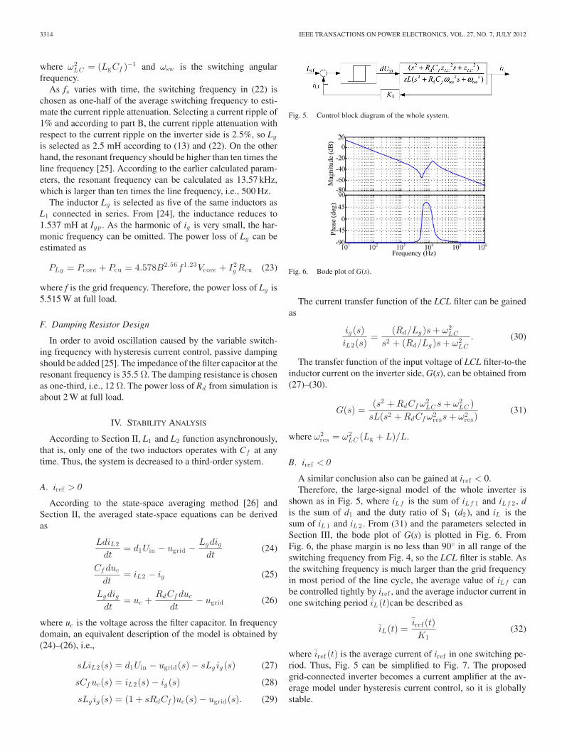
Fig. 5. Control block diagram of the whole system.
Fig. 6. Bode plot of G(s).
The current transfer function of the LCL filter can be gainedas
ig (s)iL2(s)
=(Rd/Lg )s + ω2
LC
s2 + (Rd/Lg )s + ω2LC
. (30)
The transfer function of the input voltage of LCL filter-to-theinductor current on the inverter side, G(s), can be obtained from(27)–(30).
G(s) =(s2 + RdCf ω2
LC s + ω2LC )
sL(s2 + RdCf ω2ress + ω2
res)(31)
where ω2res = ω2
LC (Lg + L)/L.
B. iref < 0
A similar conclusion also can be gained at iref < 0.Therefore, the large-signal model of the whole inverter is
shown as in Fig. 5, where iLf is the sum of iLf 1 and iLf 2 , dis the sum of d1 and the duty ratio of S1 (d2), and iL is thesum of iL 1 and iL 2 . From (31) and the parameters selected inSection III, the bode plot of G(s) is plotted in Fig. 6. FromFig. 6, the phase margin is no less than 90◦ in all range of theswitching frequency from Fig. 4, so the LCL filter is stable. Asthe switching frequency is much larger than the grid frequencyin most period of the line cycle, the average value of iLf canbe controlled tightly by iref , and the average inductor current inone switching period iL (t)can be described as
iL (t) =iref (t)K1
(32)
where iref (t) is the average current of iref in one switching pe-riod. Thus, Fig. 5 can be simplified to Fig. 7. The proposedgrid-connected inverter becomes a current amplifier at the av-erage model under hysteresis current control, so it is globallystable.

YAO AND XIAO: TWO-SWITCH DUAL-BUCK GRID-CONNECTED INVERTER WITH HYSTERESIS CURRENT CONTROL 3315
Fig. 7. Simplified control block diagram of the whole system.
Fig. 8. Simulation results at full load.
V. SIMULATION RESULTS
A 1-kW two-switch dual-buck grid-connected inverter hasbeen simulated to verify the theoretical analysis with the param-eters shown in Section III, and the models of the MOSFETs anddiodes used in SABER simulation software are SPW47N60C3and DSEI30, respectively.
Fig. 8 shows the simulation results at full load, where uA
and uBC (see Fig. 1) are the voltages before the LCL filter.From Fig. 8, S1 and S2 operate in high frequency at negativeand positive half line cycles, respectively. The voltage stressesof S1 and S2 are Uin and the voltage stresses of S3 and S4are Uop . The inductor L2 operates at positive half line cycle,whereas L1 operates at negative half line cycle. Therefore, S3and S4 can realize zero-current switching (ZCS). The voltagesuA and uBC are unipolar at negative and positive half line cycles,respectively. As the models of the power devices are practicalmodels, the voltages uds3 and uds4 sustain |uo | before they reachUop . After that, they are divided by CS and CD . Therefore, thesimulation verifies the theoretical analysis.
The simulated harmonic components of iL operating underrated condition are shown in Fig. 9. From Fig. 9, the harmonicfrequency of iL mainly lies between 50 and 90 kHz, which is
Fig. 9. Harmonic spectrum of iL .
Fig. 10. Harmonic spectrum of ig with simulation results.
Fig. 11. Loss Ploss with simulation results.
in accordance with the switching frequency range shown inFig. 4.
Fig. 10 presents the harmonic spectrum of ig . From Fig. 10,the harmonic component is far less than the limits in IEEE Std.929-2000. The total harmonic distortion (THD) of ig is 2.25%,which is less than the limit in IEEE Std. 929-2000, i.e., <5%.
Fig. 11 shows the power losses of the power devices anddamping resistor (Ploss). From Fig. 11, Ploss increases with Po .
VI. EXPERIMENTAL RESULTS
A 1-kW prototype has been constructed to verify the theoret-ical analysis with the parameters shown in Section III, and theMOSFETs and diodes used in the prototype are SPW47N60C3and DSEI8-06A, respectively.
Fig. 12 gives the experimental results at full load. The differ-ence between Figs. 8 and 12(a) is that the divided voltage by CS
and CD in Fig. 8 is different from that in Fig. 12(a). The mainreason for this is that the model of the diode in simulation is dif-ferent from that in the practical diode, which cannot be found inthe simulation software. As shown in Fig. 12(b), the inductorsL1 and L2 operate at negative and positive half line cycles,respectively. The waveform quality of ig is good. From
3316 IEEE TRANSACTIONS ON POWER ELECTRONICS, VOL. 27, NO. 7, JULY 2012
Fig. 12. Experimental results at full load. (a) Waveforms of ugrid , uds1 , uds2 ,uds3 , and uds4 . (b) Waveforms of ig , iL 2 , and iL 1 . (c) Waveforms of ugrid ,uA , and uBC .
Fig. 12(c), the proposed grid-connected operates at unipolarmodulation.
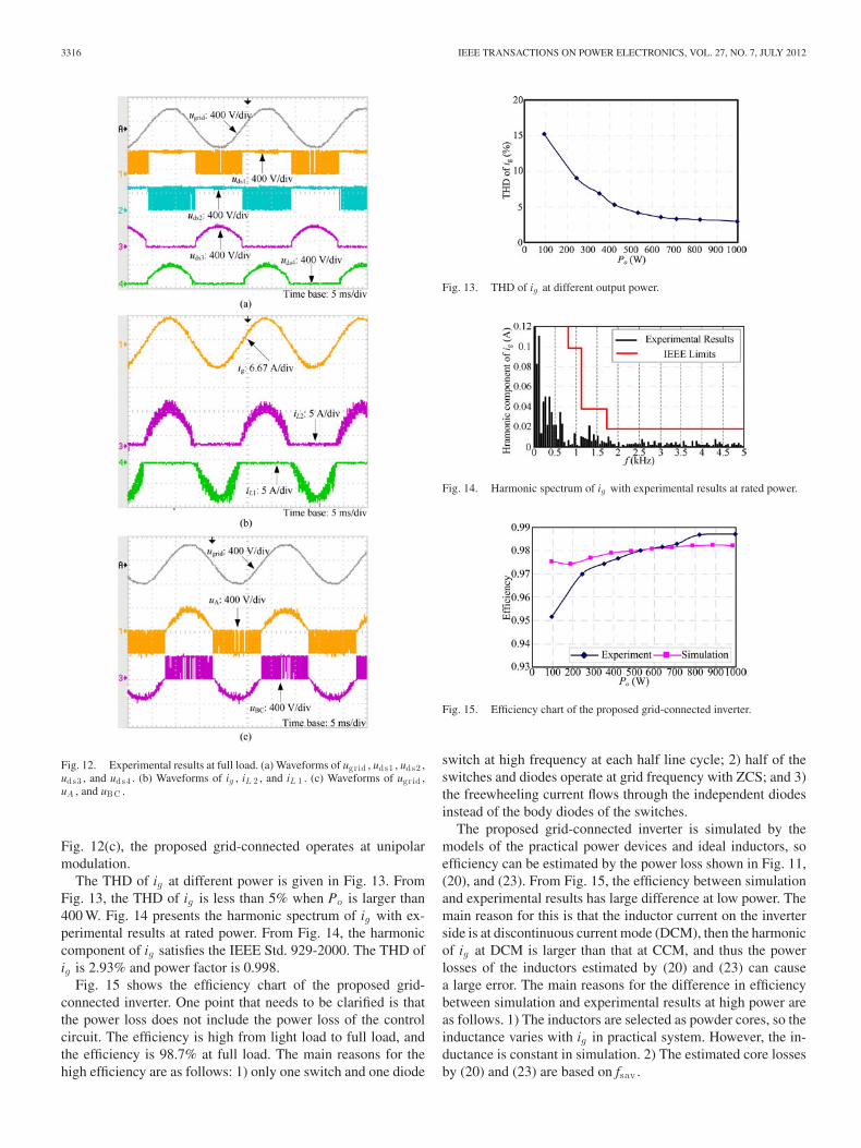
The THD of ig at different power is given in Fig. 13. FromFig. 13, the THD of ig is less than 5% when Po is larger than400 W. Fig. 14 presents the harmonic spectrum of ig with ex-perimental results at rated power. From Fig. 14, the harmoniccomponent of ig satisfies the IEEE Std. 929-2000. The THD ofig is 2.93% and power factor is 0.998.
Fig. 15 shows the efficiency chart of the proposed grid-connected inverter. One point that needs to be clarified is thatthe power loss does not include the power loss of the controlcircuit. The efficiency is high from light load to full load, andthe efficiency is 98.7% at full load. The main reasons for thehigh efficiency are as follows: 1) only one switch and one diode
Fig. 13. THD of ig at different output power.
Fig. 14. Harmonic spectrum of ig with experimental results at rated power.
Fig. 15. Efficiency chart of the proposed grid-connected inverter.
switch at high frequency at each half line cycle; 2) half of theswitches and diodes operate at grid frequency with ZCS; and 3)the freewheeling current flows through the independent diodesinstead of the body diodes of the switches.
The proposed grid-connected inverter is simulated by themodels of the practical power devices and ideal inductors, soefficiency can be estimated by the power loss shown in Fig. 11,(20), and (23). From Fig. 15, the efficiency between simulationand experimental results has large difference at low power. Themain reason for this is that the inductor current on the inverterside is at discontinuous current mode (DCM), then the harmonicof ig at DCM is larger than that at CCM, and thus the powerlosses of the inductors estimated by (20) and (23) can causea large error. The main reasons for the difference in efficiencybetween simulation and experimental results at high power areas follows. 1) The inductors are selected as powder cores, so theinductance varies with ig in practical system. However, the in-ductance is constant in simulation. 2) The estimated core lossesby (20) and (23) are based on fsav .

YAO AND XIAO: TWO-SWITCH DUAL-BUCK GRID-CONNECTED INVERTER WITH HYSTERESIS CURRENT CONTROL 3317
VII. COMPARISON BETWEEN FULL-BRIDGE INVERTER AND
THE PROPOSED INVERTER
In this section, the proposed inverter and full-bridge inverterare compared with the parameters shown in Section III. Theyhave the same input-voltage utilization rate according to theanalysis in Section II.
A. Total Switching Device Power Comparison
In an inverter system, total switching device power (SDP) is ameasure of the total semiconductor device requirement, whichis an important cost indicator of an inverter system. Based onthe analysis in Section II, the rms currents of high-frequencyswitches Isrms1 and low-frequency switches Isrms2 can be ex-pressed as
Isrms1 =
√1T
∫ T /2
0(is1(t))2dt
=
√1T
∫ T /2
0(d2iL1(t))2dt ≈
√3ILpM
4(33)
Isrms2 =
√1T
∫ T /2
0(is4(t))2dt
=
√1T
∫ T /2
0(iL1(t))2dt ≈ ILp
2(34)
where M is equal to√
2Ugrid/Uin and the peak filter inductorcurrent ILp omitting the current through Cf can be estimatedas√
2Ig .The average currents of high-frequency diodes Idav1 and low-
frequency diodes Idav2 can be expressed as
Idav1 =1T
∫ T /2
0|id1(t)| dt =
1T
∫ T /2
0|(1 − d2)iL1(t)| dt
≈ ILp
2
(2π− M
2
). (35)
Idav2 =1T
∫ T /2
0|id4(t)| dt
=1T
∫ T /2
0|iL1(t)| dt ≈ ILp
π. (36)
Based upon the earlier analysis and the design guidelines inSection III, the components comparison between the proposedinverter and full-bridge inverter is illustrated in Table I. Asshown by Table I, the total SDP of the proposed inverter is alittle larger than that of full-bridge inverter. However, the SDPof the switches in the proposed inverter is lower than that offull-bridge inverter. Moreover, the voltage stress of the low-frequency switches in the proposed inverter is just equal to Uop ,which is less than that in full-bridge inverter. The number ofhigh-frequency switches at each half line cycle in the proposedinverter is half of that in the full-bridge inverter.
Although the proposed inverter has four extra independentdiodes compared with the full-bridge inverter, the shoot-through
TABLE ICOMPARISON BETWEEN FULL-BRIDGE INVERTER AND THE
PROPOSED INVERTER
problem does not exist in the proposed inverter, which can bea major detriment to the full-bridge inverter. Consequently, theproposed inverter can be used in high-reliability application. Inaddition, the freewheeling current does not flow through thebody diodes of the switches in the proposed inverter, so inde-pendent freewheeling diodes with lower reverse-recovery timecan be selected.
B. Requirement of Passive Components Comparison
Passive components, namely inductors and capacitors, arealso important parts to determining the inverter cost and vol-ume. The filter inductors and filter capacitor can be calculatedaccording to Section III. As the compared inverters have thesame filter capacitor and filter inductor on the grid side, onlythe filter inductors on the inverter side are described in Table I.The number of the filter inductors in the proposed inverter istwice than that in full-bridge inverter, but the rms current ofthe filter inductors in full-bridge inverter is
√2 times than that
in the proposed inverter. Thus, the required filter inductors inthe proposed inverter are a little larger than that in full-bridgeinverter.
The comparison between full-bridge inverter and the pro-posed inverter shows that the cost of the proposed inverter is alittle higher than that of full-bridge inverter, but the proposedinverter is very promising in high-reliability application.

3318 IEEE TRANSACTIONS ON POWER ELECTRONICS, VOL. 27, NO. 7, JULY 2012
VIII. CONCLUSION
This paper proposed a two-switch dual-buck grid-connectedinverter with hysteresis current control. Unipolar modulationhas been chosen. The operating principle, design guidelines andexample, and stability analysis have been given. The simulationand experimental results from a 1-kW two-switch dual-buckgrid-connected inverter verify the theoretical analysis. The pro-posed grid-connected inverter has the following characteristics.
1) Only one switch and one diode operate in high frequencyat each half line cycle, and half of the power devices switchat grid period with ZCS.
2) In contrast to the DBHBI, the input-voltage utilizationrate doubles, and the voltage stresses of the switches anddiodes can be reduced at the same output voltage.
3) Compared with the conventional bridge-type voltage-source inverters, the shoot-through problem does not exist.
4) Compared to the full-bridge inverter, the freewheeling cur-rent flows through the independent diodes instead of thebody diodes of the switches, so reverse-recovery loss ofthe diodes can be reduced.
5) Compared with the DBHBI and DBFBI, unipolar modu-lation is used, so weight and volume of the output filtercan be reduced.
6) Compared to the Z-source inverter, inrush current atstartup does not exist.
The comparison between full-bridge inverter and the pro-posed inverter demonstrated that the proposed inverter is moreattractive in high-reliability applications.
REFERENCES
[1] F. Blaabjerg, Z. Chen, and S. B. Kjaer, “Power electronics as efficientinterface in dispersed power generation systems,” IEEE Trans. PowerElectron., vol. 19, no. 5, pp. 1184–1194, Sep. 2004.
[2] E. Serban and H. Serban, “A control strategy for a distributed power gen-eration microgrid application with voltage- and current-controlled sourceconverter,” IEEE Trans. Power Electron., vol. 25, no. 12, pp. 2981–2992,Dec. 2010.
[3] R. I. Bojoi, L. R. Limongi, D. Roiu, and A. Tenconi, “Enhanced powerquality control strategy for single-phase inverters in distributed generationsystems,” IEEE Trans. Power Electron., vol. 26, no. 3, pp. 798–806, Mar.2011.
[4] J.-H. Kim, J.-G. Kim, Y.-H. Ji, Y.-C. Jung, and C.-Y. Won, “An islandingdetection method for a grid-connected system based on the goertzel algo-rithm,” IEEE Trans. Power Electron., vol. 26, no. 4, pp. 1049–1055, Apr.2011.
[5] J. Hu, L. Shang, Y. He, and Z. Q. Zhu, “Direct active and reactive powerregulation of grid-connected DC/AC converters using sliding mode controlapproach,” IEEE Trans. Power Electron., vol. 26, no. 1, pp. 210–222, Jan.2011.
[6] J. Dannehl, F. W. Fuchs, and P. B. Thøgersen, “PI state space currentcontrol of grid-connected PWM converters with LCL filters,” IEEE Trans.Power Electron., vol. 25, no. 9, pp. 2320–2330, Sep. 2010.
[7] J. Alonso-Martınez, J. Carrasco, and S. Arnaltes, “Table-based directpower control: A critical review for microgrid applications,” IEEE Trans.Power Electron., vol. 25, no. 12, pp. 2949–2961, Dec. 2010.
[8] Y.-H. Liao and C.-M. Lai, “Newly-constructed simplified single-phasemultistring multilevel inverter topology for distributed energy resources,”IEEE Trans. Power Electron., vol. 26, no. 9, pp. 2386–2392, Sep. 2011.
[9] J. L. Agorreta, M. Borrega, J. Lopez, and L. Marroyo, “Modeling andcontrol of N-paralleled grid-connected inverters with LCL filter coupleddue to grid impedance in PV plants,” IEEE Trans. Power Electron.,vol. 26, no. 3, pp. 770–785, Mar. 2011.
[10] W. Zhao, D. D.-C. Lu, and V. G. Agelidis, “Current control of grid-connected boost inverter with zero steady-state error,” IEEE Trans. PowerElectron., vol. 26, no. 10, pp. 2825–2834, Oct. 2011.
[11] Z. Yao, L. Xiao, and Y. Yan, “Seamless transfer of single-phase grid-interactive inverters between grid-connected and stand-alone modes,”IEEE Trans. Power Electron., vol. 25, no. 6, pp. 1597–1603, Jun. 2010.
[12] F. Z. Peng, “Z-source inverter,” IEEE Trans. Ind. Appl., vol. 39, no. 2,pp. 504–510, Mar./Apr. 2003.
[13] Z. Zhou, X. Zhang, P. Xu, and W. X. Shen, “Single-phase uninterruptiblepower supply based on Z-source inverter,” IEEE Trans. Ind. Electron.,vol. 55, no. 8, pp. 2997–3004, Aug. 2008.
[14] J. Liu and Y. Yan, “A novel hysteresis current controlled dual buck halfbridge inverter,” in Proc. IEEE 34th Ann. Power Electron. Specialist Conf.(PESC), 2003, pp. 1615–1620.
[15] Z. Yao, L. Xiao, and Y. Yan, “Control strategy for series and paralleloutput dual-buck half bridge inverters based on DSP control,” IEEETrans. Power Electron., vol. 24, no. 2, pp. 434–444, Feb. 2009.
[16] Z. Yao, L. Xiao, and Y. Yan, “Dual-buck full-bridge inverter with hysteresiscurrent control,” IEEE Trans. Ind. Electron., vol. 56, no. 8, pp. 3153–3160,Aug. 2009.
[17] L. Corradini, A. Bjeletic, R. Zane, and D. Maksimovic, “Fully digitalhysteretic modulator for DC–DC switching converters,” IEEE Trans.Power Electron., vol. 26, no. 10, pp. 2969–2979, Oct. 2011.
[18] A. Shukla, A. Ghosh, and A. Joshi, “Hysteresis modulation of multilevelinverters,,” IEEE Trans. Power Electron., vol. 26, no. 5, pp. 1396–1409,May 2011.
[19] M. Mohseni, S. M. Islam, and M. A. Masoum, “Enhanced hysteresis-basedcurrent regulators in vector control of DFIG wind turbines,” IEEE Trans.Power Electron., vol. 26, no. 1, pp. 223–234, Jan. 2011.
[20] M. Mohseni and S. M. Islam, “A new vector-based hysteresis currentcontrol scheme for three-phase PWM voltage-source inverters,” IEEETrans. Power Electron., vol. 25, no. 9, pp. 2299–2309, Sep. 2010.
[21] Y. Chen and Y. Kang, “The variable-bandwidth hysteresis-modulationsliding-mode control for the PWM–PFM converters,” IEEE Trans. PowerElectron., vol. 26, no. 10, pp. 2727–2734, Oct. 2011.
[22] A. Z. Albanna and C. J. Hatziadoniu, “Harmonic modeling of hysteresisinverters in frequency domain,” IEEE Trans. Power Electron., vol. 25,no. 5, pp. 1110–1114, May 2010.
[23] N. Prabhakar and M. K. Mishra, “Dynamic hysteresis current control tominimize switching for three-phase four-leg VSI topology to compensatenonlinear load,” IEEE Trans. Power Electron., vol. 25, no. 8, pp. 1935–1942, Aug. 2010.
[24] Powder Cores Design Manual and Catalog. (2008). [Online]. Available:http://www.mag-inc.com
[25] M. Liserre, F. Blaabjerg, and S. Hansen, “Design and control of an LCL-filter-based three-phase active rectifier,” IEEE Trans. Ind. Appl., vol. 41,no. 5, pp. 1281–1291, Sep./Oct. 2005.
[26] T. Suntio, “Unified average and small-signal modeling of direct-on-timecontrol,” IEEE Trans. Ind. Electron., vol. 53, no. 1, pp. 287–295, Feb.2006.
Zhilei Yao was born in Jiangsu, China, in 1981.He received the B.S. and M.S. degrees in electri-cal engineering from Nanjing University of Aero-nautics and Astronautics, Nanjing, China, in 2003and 2006, respectively, where he is currently work-ing toward the Ph.D. degree in electrical engineeringat the Jiangsu Key Laboratory of New Energy Gen-eration and Power Conversion.
He is also with the School of Electrical Engineer-ing, Yancheng Institute of Technology, Yancheng,China. He holds eight patents, and is the author or
coauthor of more than 40 technical papers. His current research interests in-clude dc–dc converters, inverters, and distributed power generation.
Lan Xiao (M’06) was born in Zhejiang, China, in1971. She received the B.S. and Ph.D. degrees in elec-trical engineering from Nanjing University of Aero-nautics and Astronautics (NUAA), Nanjing, China,in 1993 and 1998, respectively.
In 1999, she joined the College of Automation En-gineering, NUAA, as a Faculty Member, where sheis currently a Professor with the Jiangsu Key Labora-tory of New Energy Generation and Power Conver-sion. She is the author or coauthor of more than 50technical papers in journals and conferences. Her cur-
rent research interests include soft-switching dc/dc converters, soft-switchinginverters, and renewable energy generation system.