a new manufacturing process for high volume production of ceramic
TRANSCRIPT
A New Manufacturing Process for High Volume Production of Ceramic Column Grid Array Modules
The International Journal of Microcircuits and Electronic Packaging, Volume 23, Number 4, Fourth Quarter, 2000 (ISSN 1063-1674)
© International Microelectronics And Packaging Society 451
A New Manufacturing Process for High VolumeProduction of Ceramic Column Grid ArrayModulesLouis Achard and Isabel DeSousaMLC B/A EngineeringIBM Canada23, Airport BoulevardBromont, QuebecCanada J2L 1A3Phone: 450-534-6475/6601Fax: 450-534-6800/7171e-mails: [email protected] and [email protected]
Abstract
Ceramic column grid array modules have been gaining popularity for electronic packaging of high performance asics with over 625I/Os. To support this growing demand, a new assembly line had to be developed, providing not only high capacity, but also competi-tive costs and a level of quality suitable for high-end applications.This paper describes how the various aspects of the new assembly line, based on a new column attach process (CLASP), weredeveloped and optimized. More specifically, the paper will describe the use of multi-up processing, a combination of customized toolsand standard surface mount equipment, the integration of a semi-aqueous flux cleaning process, automated column planarization,and finally the development of automated column inspection technology. The concepts and processes were developed for both1.27mm and 1.00mm pitch products on ceramic carriers up to 2600 I/Os.
Key words:Ceramic Column Grid Array, Automation, Flip Chip Carriers,and Surface Mount Technology.
1. Introduction
Ceramic Column Grid Array (CCGA) packages have provento be very reliable high I/O count modules, with up to 2600 I/Oson a 52.5 mm ceramic. These packages offer several advan-tages, namely, high-density interconnection, compatibility withSMT assembly, superior thermal and electrical performance.CCGAs are offered in a variety of dimensions covering the JEDECspecifications in 1.27 mm and 1 mm pitch.
CCGA packages are interconnected to circuit boards throughan array of 10/90 solder columns with standard lengths of 50 or
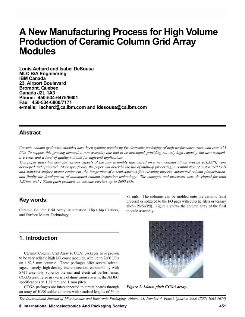
87 mils. The columns can be molded onto the ceramic (castprocess) or soldered to the I/O pads with eutectic filets or ternaryalloy (Pb/Sn/Pd). Figure 1 shows the column array of the finalmodule assembly.
Figure 1. 1.0mm pitch CCGA array.
© International Microelectronics And Packaging Society
The International Journal of Microcircuits and Electronic Packaging, Volume 23, Number 4, Fourth Quarter, 2000 (ISSN 1063-1674)
Intl. Journal of Microcircuits and Electronic Packaging
452
Until recently, manufacturing of these components had beena manual and relatively low volume process (cast process). Thisprocess requires a high temperature reflow (above 300°C), andtherefore needs to happen before other bond and assembly (B/A)operations. It requires electrical testing to be performed with prob-ing on the columns. This is not desirable from a cost/qualitystandpoint, since columns are exposed to damage during subse-quent operations, and testing on columns is more expensive thantesting on substrate I/O pads.
Cast column replacement is also an expensive and low yieldprocess. Finally, this type of process has problems typically asso-ciated with manual operations, such as ergonomic issues, highcost, and low capacity.
2. Objectives
When IBM examined possible options to implement a highcapacity manufacturing operation, the following objectives hadto be achieved, namely;
· Competitive cost,· Minimum column handling / damage,· Possibility to perform electrical testing before attaching col-
umns,· Maximum throughput,· Minimum technological risk,· Flexibility to run different form factors with minimum set-
up costs,· Environmentally friendly,· Quick and easy module re-columning,· Compatibility with second level processes.
3. Strategy
One of the main conditions to achieve these goals was to imple-ment a low temperature process. This was required to bring col-umn attach at the very end of the module B/A process, allowingelectrical testing to be carried out before column attach, and mini-mizing handling of the finished modules before shipping to cus-tomers. The low temperature process would also allow easy re-moval of the columns by re-melting the solder joint in a conven-tional rework process.
The main challenge for this low temperature process, how-ever, was to provide a column solder joint which could allowremoval of a module from a card without leaving many columnson the card site, unlike a conventional eutectic tin-lead solderjoint. This led to the development of a new process called CLASP(Column Last Solder Attach Process), based on a Pd doped eu-tectic solder, to attach columns to the ceramic substrate. The
developments of this process, the metallurgy of the column struc-ture, its performance and reliability, as well as the card reworkprocess are described in detail in References1,2.
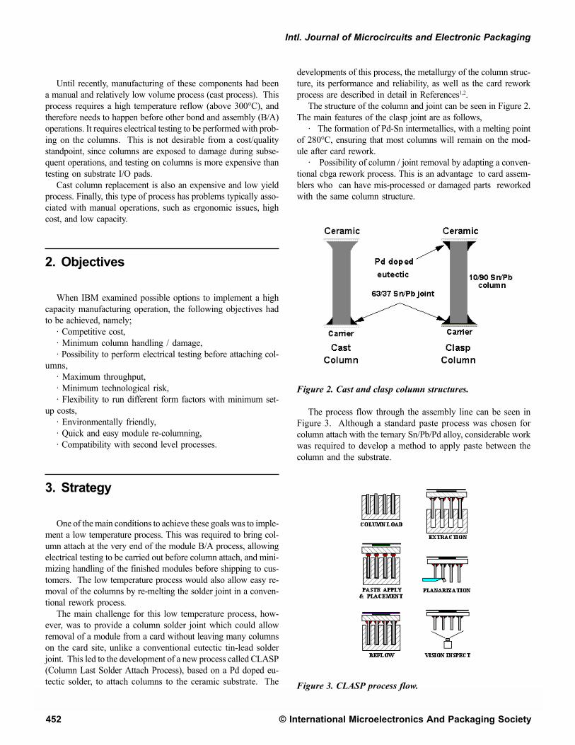
The structure of the column and joint can be seen in Figure 2.The main features of the clasp joint are as follows,
· The formation of Pd-Sn intermetallics, with a melting pointof 280°C, ensuring that most columns will remain on the mod-ule after card rework.
· Possibility of column / joint removal by adapting a conven-tional cbga rework process. This is an advantage to card assem-blers who can have mis-processed or damaged parts reworkedwith the same column structure.
Figure 2. Cast and clasp column structures.
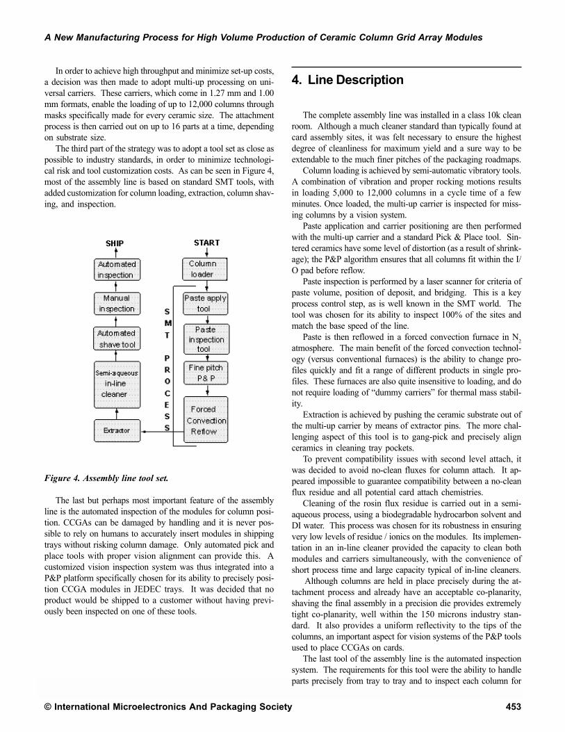
The process flow through the assembly line can be seen inFigure 3. Although a standard paste process was chosen forcolumn attach with the ternary Sn/Pb/Pd alloy, considerable workwas required to develop a method to apply paste between thecolumn and the substrate.
Figure 3. CLASP process flow.
A New Manufacturing Process for High Volume Production of Ceramic Column Grid Array Modules
The International Journal of Microcircuits and Electronic Packaging, Volume 23, Number 4, Fourth Quarter, 2000 (ISSN 1063-1674)
© International Microelectronics And Packaging Society 453
In order to achieve high throughput and minimize set-up costs,a decision was then made to adopt multi-up processing on uni-versal carriers. These carriers, which come in 1.27 mm and 1.00mm formats, enable the loading of up to 12,000 columns throughmasks specifically made for every ceramic size. The attachmentprocess is then carried out on up to 16 parts at a time, dependingon substrate size.
The third part of the strategy was to adopt a tool set as close aspossible to industry standards, in order to minimize technologi-cal risk and tool customization costs. As can be seen in Figure 4,most of the assembly line is based on standard SMT tools, withadded customization for column loading, extraction, column shav-ing, and inspection.
Figure 4. Assembly line tool set.
The last but perhaps most important feature of the assemblyline is the automated inspection of the modules for column posi-tion. CCGAs can be damaged by handling and it is never pos-sible to rely on humans to accurately insert modules in shippingtrays without risking column damage. Only automated pick andplace tools with proper vision alignment can provide this. Acustomized vision inspection system was thus integrated into aP&P platform specifically chosen for its ability to precisely posi-tion CCGA modules in JEDEC trays. It was decided that noproduct would be shipped to a customer without having previ-ously been inspected on one of these tools.
4. Line Description
The complete assembly line was installed in a class 10k cleanroom. Although a much cleaner standard than typically found atcard assembly sites, it was felt necessary to ensure the highestdegree of cleanliness for maximum yield and a sure way to beextendable to the much finer pitches of the packaging roadmaps.
Column loading is achieved by semi-automatic vibratory tools.A combination of vibration and proper rocking motions resultsin loading 5,000 to 12,000 columns in a cycle time of a fewminutes. Once loaded, the multi-up carrier is inspected for miss-ing columns by a vision system.
Paste application and carrier positioning are then performedwith the multi-up carrier and a standard Pick & Place tool. Sin-tered ceramics have some level of distortion (as a result of shrink-age); the P&P algorithm ensures that all columns fit within the I/O pad before reflow.
Paste inspection is performed by a laser scanner for criteria ofpaste volume, position of deposit, and bridging. This is a keyprocess control step, as is well known in the SMT world. Thetool was chosen for its ability to inspect 100% of the sites andmatch the base speed of the line.
Paste is then reflowed in a forced convection furnace in N2atmosphere. The main benefit of the forced convection technol-ogy (versus conventional furnaces) is the ability to change pro-files quickly and fit a range of different products in single pro-files. These furnaces are also quite insensitive to loading, and donot require loading of “dummy carriers” for thermal mass stabil-ity.
Extraction is achieved by pushing the ceramic substrate out ofthe multi-up carrier by means of extractor pins. The more chal-lenging aspect of this tool is to gang-pick and precisely alignceramics in cleaning tray pockets.
To prevent compatibility issues with second level attach, itwas decided to avoid no-clean fluxes for column attach. It ap-peared impossible to guarantee compatibility between a no-cleanflux residue and all potential card attach chemistries.
Cleaning of the rosin flux residue is carried out in a semi-aqueous process, using a biodegradable hydrocarbon solvent andDI water. This process was chosen for its robustness in ensuringvery low levels of residue / ionics on the modules. Its implemen-tation in an in-line cleaner provided the capacity to clean bothmodules and carriers simultaneously, with the convenience ofshort process time and large capacity typical of in-line cleaners. Although columns are held in place precisely during the at-tachment process and already have an acceptable co-planarity,shaving the final assembly in a precision die provides extremelytight co-planarity, well within the 150 microns industry stan-dard. It also provides a uniform reflectivity to the tips of thecolumns, an important aspect for vision systems of the P&P toolsused to place CCGAs on cards.
The last tool of the assembly line is the automated inspectionsystem. The requirements for this tool were the ability to handleparts precisely from tray to tray and to inspect each column for
© International Microelectronics And Packaging Society
The International Journal of Microcircuits and Electronic Packaging, Volume 23, Number 4, Fourth Quarter, 2000 (ISSN 1063-1674)
Intl. Journal of Microcircuits and Electronic Packaging
454
position with respect to the best fit of the column grid at highspeed. Such a vision system, which did not exist on the market,had to be custom built and integrated into the P&P chosen forparts handling. This type of measurement is very sensitive tocolumn tip illumination and parasitic reflections. Finding thetrue center of the columns was the key challenge for this tool.
5. Process Challenges and Issues
Paste processes have certain limitations, which had to be takeninto account while implementing and optimizing the CLASPprocess. Controlling the solder joint volume on a large numberof I/Os and optimizing fillet shape were important steps to achievehigh reliability module interconnexions. Controlling the void-ing level of the ternary alloy paste has also driven optimizationwork, resulting in unique reflow profiles.
The incoming quality of materials also has a significant im-pact on the defect level of the finished product. Solder segments,in particular, need to meet a quality level in excess of 6 sigma,simply due to the quantity of columns per module. IBM had towork closely with its suppliers to develop this level of quality inthe wire forming and cutting processes, which until then did notexist in the industry.
Solder column quality was a key in controlling factors such assolder wicking, column surface defects, notches, voids, amongother factors. Product specifications for these defects areparticularily stringent. For example, any notch or void beyond0.13mm is considered rejectable.
The next challenge was to control the uniformity of solderpaste deposits. In this case, the key factors were the precision ofthe multi-up carriers, a tight control of the dimensions of thesolder segments, and the use of automated paste inspection equip-ment. It was also found that paste rheology had to be controlledwithin tighter limits than SMT standards.
Contamination by fibers or particles was found to be a minorcontributor to yield losses; this is attributed to the clean roomenvironment. The choice of multi-up carriers proved to be finefor throughput and productivity, but came at the expense of cost(machining over 10,000 holes), fragility (higher probability ofdamaging one of the carrier holes), and the difficulty of cleaning.Special magazines and rigorous handling were necessary to com-pensate for these drawbacks. Carriers have to be handled duringsome cleaning steps and column loading; the ultimate goal re-mains to have a completely automated closed loop where carrierswould only travel on edge belt materiel handling systems.
Another aspect, which has driven a significant design effort,is the column shave operation. Previous techniques to cut leadcolumns required lubrication, but the integration of this processin a pick and place tool after the flux cleaning process requiredthe design of a dry process. This was achieved with the properselection of blade material and the optimization of die and knife.
6. Card Attach Considerations
Assembly of CCGAs on cards had been a difficult process inthe past, and the introduction of the CLASP process was an op-portunity to improve on some of these aspects. The first issuewas with module alignment on the pick and place tools. Majorcustomers wanted a robust way to align parts from the position ofthe tips of the columns (as opposed to the body of the ceramic, amethod still widely used) especially on the fine pitch (1mm)modules. IBM worked with some of the major placement equip-ment suppliers to develop an illumination system specifically forCCGAs. These systems allow finding all of the column posi-tions on the module and performing a best fit to the card pads,for optimal yield at card assembly. The performance of thesevision systems (as well as those of any placement equipment)was also improved by the more uniform reflectivity of the newdry shaved surface of the column tips. The machine vision in-spection of all columns carried out by IBM before shipping en-sures that no column irregularity will affect pick and place visionsystems.
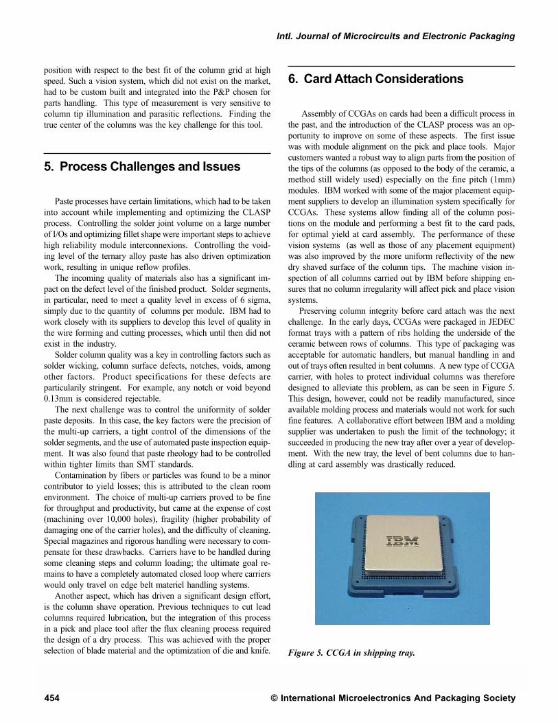
Preserving column integrity before card attach was the nextchallenge. In the early days, CCGAs were packaged in JEDECformat trays with a pattern of ribs holding the underside of theceramic between rows of columns. This type of packaging wasacceptable for automatic handlers, but manual handling in andout of trays often resulted in bent columns. A new type of CCGAcarrier, with holes to protect individual columns was thereforedesigned to alleviate this problem, as can be seen in Figure 5.This design, however, could not be readily manufactured, sinceavailable molding process and materials would not work for suchfine features. A collaborative effort between IBM and a moldingsupplier was undertaken to push the limit of the technology; itsucceeded in producing the new tray after over a year of develop-ment. With the new tray, the level of bent columns due to han-dling at card assembly was drastically reduced.
Figure 5. CCGA in shipping tray.
A New Manufacturing Process for High Volume Production of Ceramic Column Grid Array Modules
The International Journal of Microcircuits and Electronic Packaging, Volume 23, Number 4, Fourth Quarter, 2000 (ISSN 1063-1674)
© International Microelectronics And Packaging Society 455
Column tilt also became a concern for CCGA customers, es-pecially those using the ceramic to align CCGAs on cards. Col-umn tilt is inherent to the attachment process and does not affectmodule reliability, as long as it is below 11 degree after cardattach. When CLASP was initially introduced, the average col-umn tilt was 4.5 degree. It was recently reduced to 2.5 degree bymodifying the shaving tool design. This will contribute to addi-tional placement accuracy and reduced tilt after card attach.
The final card attach issue was card rework. As discussed inReference1, card rework had to be optimized for the new CLASPstructure, using a specific type of hot gas rework tool and follow-ing a recommended procedure documented by IBM3,4. Any mod-ule damaged at card assembly, from handling or as a result ofcard rework, can be returned to IBM for quick re-columning, at afraction of the cost of a new module. The rework process canaccept modules with columns at any level of damage.
7. Conclusion
This high volume integrated new CCGA manufacturing pro-cess has been in operation for over a year now, and has producednearly 2 million modules. The original objectives were largelymet and the project is now in the cost reduction phase of thetechnology cycle. Both IBM and card assemblers have acquiredan expertise that makes CCGAs a well understood and acceptedtechnology for high performance electronic packaging.
Expansion of the assembly line has since been undertaken, asforecasts predict a strong growth in demand for CCGA modulesin the short and long term. The basic and flexible design of theline will be the starting point for the introduction of lead-freeCLASP and future generations of product such as 0.8mm pitchproducts, and form factors beyond the current maximum size of52 mm x 52 mm. I/O counts will probably reach over 3000 withinthe next 3 years.
Acknowledgments
The authors wish to acknowledge the contributions of J.Dankelman and S. Dussault during the initial study of the lineconcept, G. Mercier and Y. Ferland for the design of key tools,M. Martel and M. Côté for the development of the cleaningprocess, M. Bonneville for developing automated inspection., M.Robert for developing shipping trays, and finally J. Dery for valu-able input.
References
1. S. Ray, M. Interrante, L. Achard, M. Cole, and I. De Sousa, etal., “Clasp Ceramic Grid Array Technology for Flip ChipCarriers”, Proceedings of Semicon West 99, San Jose, Cali-fornia, pp. F1-F7, July 1999.
2. S. Ray, M. Cole, and L. Goldman, et al., “ Clasp CeramicColumn Grid Array Technology and Line Qualification Re-port”, IBM Internal Report, pg. 3, March 1999.
3. C. Milkovich and L. Jimarez, “Ceramic Column Grid ArrayAssembly and Rework”, IBM P/N APD-SCC-201.0, pp. 27-35, March 1998.
4 C. Milkovich and J. Nash, “1mm CCGA Assembly and Re-work Development & T1 Hardware build”, IBM TechnicalReport, pp. 2-4, April 1997.
About the authors
Louis Achard is currently Staff Engineer at the IBM micro-electronics packaging facility in Bromont, Canada. He receiveda B.Eng. Degree and a M. Eng. Degree from McGill Universityin Mechanical Engineering. He joined IBM in 1985, and hassince then been involved in various aspects of manufacturingtechnologies for microelectronic packaging and substrate manu-facturing. He has been responsible for ceramic column attachtechnology for the last four years.
Isabel De Sousa is also Staff Engineer at IBM in Bromont.She has an Engineering Degree in Physics and M.Sc.A Degreein Materials from Ecole Polytechnique de Montreal. She hasworked for IBM Canada for ten years, and is process engineerfor the column technology since 1997.