a novel coupled inductor z-source three-level inverter
TRANSCRIPT
A novel coupled inductorZ-source three-level inverter
Xiaogang Wanga), Hua Liu, and Yitao LiCollege of Mechanical and Electrical Engineering, Guangzhou University,
230 Waihuan Xi Road, Guangzhou 510006, China
Abstract: A novel Z-source three-level inverter based on coupled inductors
is proposed. The two inductors in traditional Z-source impedance network
are replaced by two coupled inductors. The operating principle is described
and the equations of boost factor and voltage stresses are deduced. Compar-
isons are made with other Z-source three-level inverters, especially the
multicell switched inductor Z-source three-level inverter. The two topologies
have same boost factor if a specific condition is met, but the proposed
inverter uses less components and therefore the reliability is improved.
SVPWM method for conventional three-level NPC inverter is easy to apply
to the novel inverter after a simple modification. Simulations are conducted
to verify the theoretical analysis.
Keywords: Z-source inverter, coupled inductor, switched inductor, three-
level, neutral-point-clamped
Classification: Power devices and circuits
References
[1] V. Yaramasu, et al.: “Predictive control for low-voltage ride-through enhance-ment of three-level-boost and NPC-converter based PMSG wind turbine,”IEEE Trans. Ind. Electron. 61 (2014) 6832 (DOI: 10.1109/TIE.2014.2314060).
[2] S. Wang, et al.: “Hybrid single-carrier-based pulse width modulation schemefor single-phase three-level neutral-point-clamped grid-side converters inelectric railway traction,” IET Power Electron. 9 (2016) 2500 (DOI: 10.1049/iet-pel.2015.0656).
[3] R. Maheshwari, et al.: “Design of neutral-point voltage controller of a three-level NPC inverter with small DC-link capacitors,” IEEE Trans. Ind. Electron.60 (2013) 1861 (DOI: 10.1109/TIE.2012.2202352).
[4] P. C. Loh, et al.: “Comparative evaluation of pulse width modulation strategiesfor Z-source neutral-point-clamped inverter,” IEEE Trans. Power Electron. 22(2007) 1005 (DOI: 10.1109/TPEL.2007.895015).
[5] P. C. Loh, et al.: “Three-level Z-source inverters using a single LC impedancenetwork,” IEEE Trans. Power Electron. 22 (2007) 706 (DOI: 10.1109/TPEL.2007.892433).
[6] P. C. Loh, et al.: “Operational analysis and modulation control of three-levelZ-source inverters with enhanced output waveform quality,” IEEE Trans.Power Electron. 24 (2009) 1767 (DOI: 10.1109/TPEL.2009.2014651).
[7] O. Husev, et al.: “Single phase three-level neutral-point-clamped quasi-Z-source inverter,” IET Power Electron. 8 (2015) 1 (DOI: 10.1049/iet-pel.2013.0904).
© IEICE 2017DOI: 10.1587/elex.14.20170647Received June 22, 2017Accepted July 3, 2017Publicized July 14, 2017Copyedited August 10, 2017
1
LETTER IEICE Electronics Express, Vol.14, No.15, 1–12
[8] W. Mo, et al.: “Trans-Z-source and Γ-Z-source neutral-point-clampedinverters,” IET Power Electron. 8 (2015) 371 (DOI: 10.1049/iet-pel.2014.0725).
[9] M. Sahoo, et al.: “A three-level LC-switching-based voltage boost NPCinverter,” IEEE Trans. Ind. Electron. 64 (2017) 2876 (DOI: 10.1109/TIE.2016.2636120).
[10] X. Wang and J. Zhang: “Neutral-point potential balancing method forswitched-inductor Z-source three-level inverter,” J. Electr. Eng. Technol. 12(2017) 1203 (DOI: 10.1109/JSSC.2012.2217874).
[11] G. Zhu, et al.: “Modeling and analysis of coupled inductors in powerconverters,” IEEE Trans. Power Electron. 26 (2011) 1355 (DOI: 10.1109/TPEL.2010.2079953).
[12] A. Battiston, et al.: “A novel quasi-Z-source inverter topology with specialcoupled inductors for input current ripples cancellation,” IEEE Trans. PowerElectron. 31 (2016) 2409 (DOI: 10.1109/TPEL.2015.2429593).
[13] H. F. Ahmed, et al.: “Switched-coupled-inductor quasi-Z-source inverter,”IEEE Trans. Power Electron. 31 (2016) 1241 (DOI: 10.1109/TPEL.2015.2414971).
[14] B. Poorali, et al.: “High step-up Z-source DC–DC converter with coupledinductors and switched capacitor cell,” IET Power Electron. 8 (2015) 1394(DOI: 10.1049/iet-pel.2014.0200).
[15] M. Banaei, et al.: “Extended switching algorithms based space vector controlfor five-level quasi-Z-source inverter with coupled inductors,” IET PowerElectron. 7 (2014) 1509 (DOI: 10.1049/iet-pel.2013.0499).
1 Introduction
The three-level neutral-point-clamped (NPC) inverter has many advantages over
two-level inverter: lower switching device voltage stress, better harmonic perform-
ance with lower operating frequency and smaller output filters [1, 2, 3]. However,
the conventional three-level NPC inverter can only behave as a step-down con-
verter, whose input dc voltage must be greater than its output ac line voltage
amplitude, which limits its application.
Z-source inverter (ZSI) is one of the most promising topologies. An “X-
shaped” impedance network is employed in conventional two-level ZSI, which
consists of two inductors and two capacitors. The input dc voltage and the bridge
circuit are connected to the two ports of the impedance network respectively. The
impedance network can boost the input dc voltage with the help of shoot-through
operation, thus the input dc voltage level can be reduced. Moreover, shoot-through
becomes a normal state, so the reliability is improved.
The Z-source concept can also be applied to three-level inverters. P. C. Loh
et al. proposed a dual-Z-source three-level inverter [4], which uses two sets of
Z-source impedance networks and therefore increases the cost. The single Z-source
topology is proposed in [5, 6] and it uses only half the passive elements and only
one dc voltage source. Compared to the dual Z-source inverter, the single Z-source
inverter has almost identical performance. Quasi-Z-source inverter is another top-
ology derived from Z-source inverter. A single phase quasi-Z-source three-level
inverter is studied in [7]; one of its advantages is the continuous input current
© IEICE 2017DOI: 10.1587/elex.14.20170647Received June 22, 2017Accepted July 3, 2017Publicized July 14, 2017Copyedited August 10, 2017
2
IEICE Electronics Express, Vol.14, No.15, 1–12
because two inductors are directly connected to the dc voltage supply. One
disadvantage of the above Z-source three-level inverters is the inter-constraint
between its boost factor and modulation index, so their voltage gains are still not
very high. W. Mo et al. proposed a Trans-Z-source NPC inverter and a Γ-Z-source
NPC inverter [8]; each uses two coupled transformers to replace the two inductors
in the conventional Z-source impedance network. The voltage gain can be increas-
ed by designing the turns ratio of the transformer. In literature [9], a three-level LC-
switching-based voltage boost NPC inverter is discussed which uses less number
of high-power passive components. However, two extra switches are introduced
which need gating signals to turn them on and off. Another high boost factor
topology is multicell switched inductor Z-source three-level inverter [10]. Its boost
factor increases with the cell number significantly, but the number of Z-source
network components increases apparently too. Converters utilizing coupled induc-
tors have many advantages, such as low output current and voltage ripple, fast load
transient and low output decoupling capacitance [11]. Recently, many new top-
ologies based on coupled inductors are proposed [12, 13, 14, 15].
This paper presents a novel coupled inductor (CL) Z-source three-level inverter.
Section 2 introduces the inverter topology and its operating principle. Section 3
compares the proposed inverter with several other Z-source three-level inverters.
Section 4 describes the space vector pulse width modulation method. The perform-
ance of the proposed inverter is evaluated through simulation, and the results are
shown in Section 5.
2 Principle of coupled inductor Z-source three-level inverter
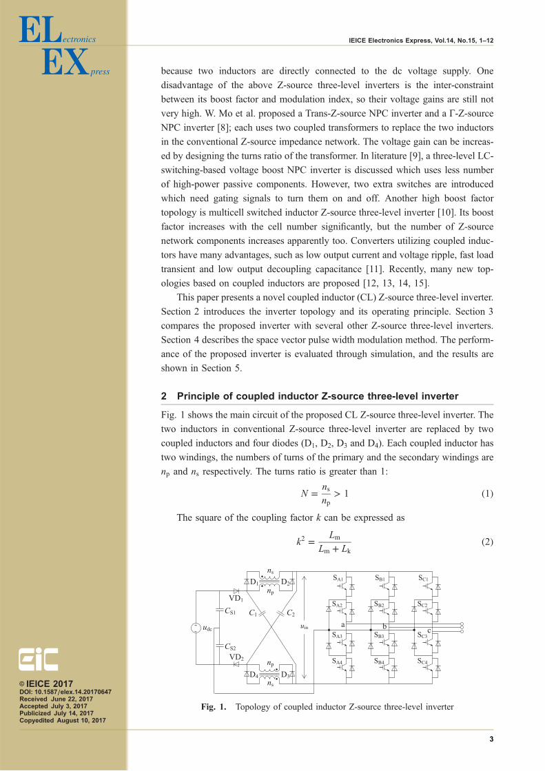
Fig. 1 shows the main circuit of the proposed CL Z-source three-level inverter. The
two inductors in conventional Z-source three-level inverter are replaced by two
coupled inductors and four diodes (D1, D2, D3 and D4). Each coupled inductor has
two windings, the numbers of turns of the primary and the secondary windings are
np and ns respectively. The turns ratio is greater than 1:
N ¼ nsnp
> 1 ð1Þ
The square of the coupling factor k can be expressed as
k2 ¼ LmLm þ Lk
ð2Þ
Fig. 1. Topology of coupled inductor Z-source three-level inverter
© IEICE 2017DOI: 10.1587/elex.14.20170647Received June 22, 2017Accepted July 3, 2017Publicized July 14, 2017Copyedited August 10, 2017
3
IEICE Electronics Express, Vol.14, No.15, 1–12
where Lm and Lk are the excitation inductance and the leakage inductance
respectively.
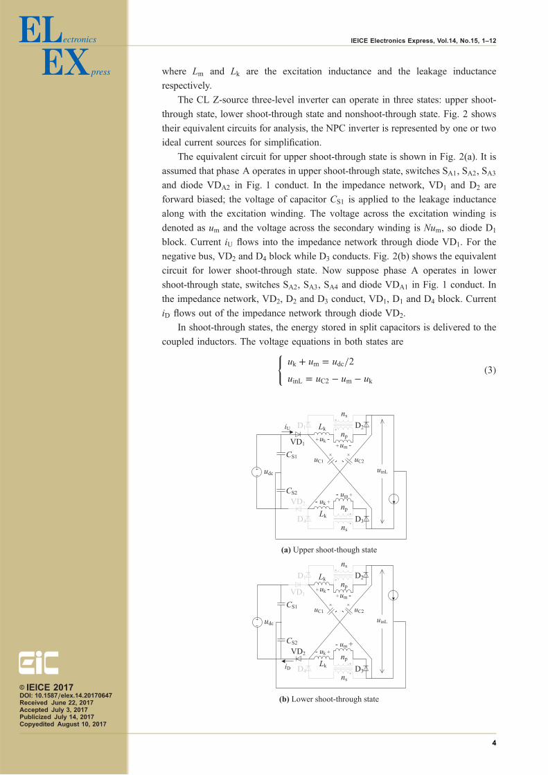
The CL Z-source three-level inverter can operate in three states: upper shoot-
through state, lower shoot-through state and nonshoot-through state. Fig. 2 shows
their equivalent circuits for analysis, the NPC inverter is represented by one or two
ideal current sources for simplification.
The equivalent circuit for upper shoot-through state is shown in Fig. 2(a). It is
assumed that phase A operates in upper shoot-through state, switches SA1, SA2, SA3and diode VDA2 in Fig. 1 conduct. In the impedance network, VD1 and D2 are
forward biased; the voltage of capacitor CS1 is applied to the leakage inductance
along with the excitation winding. The voltage across the excitation winding is
denoted as um and the voltage across the secondary winding is Num, so diode D1
block. Current iU flows into the impedance network through diode VD1. For the
negative bus, VD2 and D4 block while D3 conducts. Fig. 2(b) shows the equivalent
circuit for lower shoot-through state. Now suppose phase A operates in lower
shoot-through state, switches SA2, SA3, SA4 and diode VDA1 in Fig. 1 conduct. In
the impedance network, VD2, D2 and D3 conduct, VD1, D1 and D4 block. Current
iD flows out of the impedance network through diode VD2.
In shoot-through states, the energy stored in split capacitors is delivered to the
coupled inductors. The voltage equations in both states are
uk þ um ¼ udc=2
uinL ¼ uC2 � um � uk
(ð3Þ
(a) Upper shoot-though state
(b) Lower shoot-through state© IEICE 2017DOI: 10.1587/elex.14.20170647Received June 22, 2017Accepted July 3, 2017Publicized July 14, 2017Copyedited August 10, 2017
4
IEICE Electronics Express, Vol.14, No.15, 1–12

where uinL is the low peak value of the dc-link voltage, uk is the leakage inductance
voltage. From (2) and (3), we have um ¼ k2udc=2.
The equivalent circuit of the inverter operates in nonshoot-though state is
shown in Fig. 2(c) and Fig. 2(d). In Fig. 2(c), diodes VD1, VD2, D1 and D4
conduct, diodes D2 and D3 block. The energy in the leakage inductance begins
to release and the excitation winding voltage during which is
um ¼ k2ðudc � uC2ÞuinH1 ¼ uC2 � um � uk
(ð4Þ
where uinH1 is the high peak value of the dc-link voltage during the release of the
leakage inductance energy.
It takes time T1 for the leakage inductance energy to reach zero. Switching
period and the duty ratio of T1 are denoted as Ts and d1 respectively, so T1 ¼ d1Ts.
After that, the equivalent circuit is shown in Fig. 2(d). The voltage equations in
nonshoot-through state are as follow.
um ¼ ðudc � uC2Þ=NuinH2 ¼ uC2 � Num
(ð5Þ
where uinH2 is the high peak value of the dc-link voltage after the release of the
leakage inductance energy.
The duty cycles for the upper and lower shoot-through states are identical and
denoted as ds. Applying volt-second balance to the excitation winding we have
(c) Nonshoot-through state (leakage inductance releasing energy)
(d) Nonshoot-through state (leakage inductance finishes releasing energy)
Fig. 2. Equivalent circuits of the inverter in different operating states
© IEICE 2017DOI: 10.1587/elex.14.20170647Received June 22, 2017Accepted July 3, 2017Publicized July 14, 2017Copyedited August 10, 2017
5
IEICE Electronics Express, Vol.14, No.15, 1–12
k2udc2
� 2ds þ k2ðudc � uC2Þ � 2d1 þ ð1 � 2ds � 2d1Þ � udc � uC2N
¼ 0 ð6ÞThe impedance network capacitor voltage uC2 is deduced from (6) as
uC2 ¼ 1 � 2ð1 þ k2NÞd1 þ ðk2N � 2Þds1 � 2ds þ 2ðk2N � 1Þd1 udc ð7Þ
Because the symmetry of the impedance network, the two capacitors have equal
voltages, that is, uC1 ¼ uC2 ¼ uC. From (5) and (7), the high peak value of the dc-
link voltage is written as
uinH2 ¼ 1 � 2d1 þ 2ðk2N � 1Þds1 � 2ds þ 2ðk2N � 1Þd1 udc ¼ BCLudc ð8Þ
where BCL is the boost factor. If k2 ¼ 1 and d1 ¼ 0, (8) is simplified as
uinH2 ¼ 1 þ 2ðN � 1Þds1 � 2ds
udc ¼ BCLudc ð9Þ
The diode VD1 in lower shoot-through state and diode VD2 in upper shoot-
through state have same voltage stresses:
uVD1 ¼ uVD2 ¼ uC � udc2
¼ 1
2� 1 þ 2ðN � 1Þds
1 � 2dsudc ð10Þ
Diodes D1 and D4 have equal voltage stresses in two shoot-through states:
uD1 ¼ uD4 ¼ ðN � 1Þum ¼ N � 1
2udc ð11Þ
Diodes D2 and D3 have identical voltage stresses in nonshoot-though state:
uD2 ¼ uD3 ¼ ð1 � NÞum ¼ N � 1
Nðudc � uCÞ ¼ ðN � 1Þds
1 � 2dsudc ð12Þ
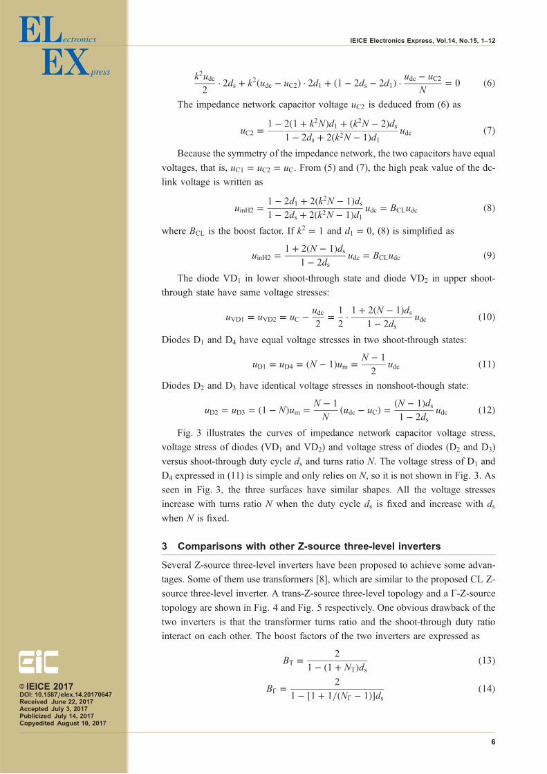
Fig. 3 illustrates the curves of impedance network capacitor voltage stress,
voltage stress of diodes (VD1 and VD2) and voltage stress of diodes (D2 and D3)
versus shoot-through duty cycle ds and turns ratio N. The voltage stress of D1 and
D4 expressed in (11) is simple and only relies on N, so it is not shown in Fig. 3. As
seen in Fig. 3, the three surfaces have similar shapes. All the voltage stresses
increase with turns ratio N when the duty cycle ds is fixed and increase with ds
when N is fixed.
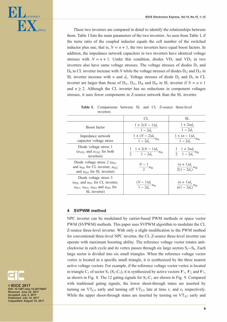
3 Comparisons with other Z-source three-level inverters
Several Z-source three-level inverters have been proposed to achieve some advan-
tages. Some of them use transformers [8], which are similar to the proposed CL Z-
source three-level inverter. A trans-Z-source three-level topology and a Γ-Z-source
topology are shown in Fig. 4 and Fig. 5 respectively. One obvious drawback of the
two inverters is that the transformer turns ratio and the shoot-through duty ratio
interact on each other. The boost factors of the two inverters are expressed as
BT ¼ 2
1 � ð1 þ NTÞds ð13Þ
B� ¼ 2
1 � ½1 þ 1=ðN� � 1Þ�ds ð14Þ© IEICE 2017DOI: 10.1587/elex.14.20170647Received June 22, 2017Accepted July 3, 2017Publicized July 14, 2017Copyedited August 10, 2017
6
IEICE Electronics Express, Vol.14, No.15, 1–12

(a) Impedance network capacitor (b) Diodes VD1 and VD2
(c) Diodes D2 and D3
Fig. 3. Impedance network capacitor voltage stress and diode voltagestresses versus turns ratio N and shoot-through duty cycle ds.
Fig. 4. Trans-Z-source three-level inverter
Fig. 5. Γ-Z-source three-level inverter© IEICE 2017DOI: 10.1587/elex.14.20170647Received June 22, 2017Accepted July 3, 2017Publicized July 14, 2017Copyedited August 10, 2017
7
IEICE Electronics Express, Vol.14, No.15, 1–12

where NT and N� are the turns ratios of the transformers used in Trans-Z-source
and Γ-Z-source topologies respectively. Their shoot-through duty ranges are
0 � ds < 1=ð1 þ NT) and 0 � ds < 1=½1 þ 1=ðN� � 1Þ� respectively. Such interac-
tions restrict their voltage boost capabilities. For CL Z-source three-level inverter
whose boost factor is expressed in (9), the turns ratio is eliminated in the
denominator. Therefore its boost factor can be very high by choosing a large N.
Another topology of Z-source three-level inverter base on switched inductor
(SL) is studied in [10] and is drawn in Fig. 6. The two switched inductors are
connected in the positive and negative buses; each of them consists of two
inductors and three diodes.
In order to improve the voltage boosting capability, multiple switched inductor
cells can be cascaded, as illustrated in Fig. 7(b). Each cell in Fig. 7(b) consists of
one inductor and three diodes, as shown in Fig. 7(a). The boost factor for the
multicell SL Z-source three-level inverter is
BSL ¼ 1 þ 2nds1 � 2ds
ð15Þ
where n is the number of SL cells. The cell number is not included in the
denominator, so high boost factor can be achieved as CL Z-source three-level
inverter.
Fig. 6. Switched inductor Z-source three-level inverter
(a) SL cell (b) Connection of SL cells
Fig. 7. Multicell switched inductor
© IEICE 2017DOI: 10.1587/elex.14.20170647Received June 22, 2017Accepted July 3, 2017Publicized July 14, 2017Copyedited August 10, 2017
8
IEICE Electronics Express, Vol.14, No.15, 1–12
These two inverters are compared in detail to identify the relationships between
them. Table I lists the main parameters of the two inverters. As seen from Table I, if
the turns ratio of the coupled inductor equals the cell number of the switched
inductor plus one, that is, N ¼ n þ 1, the two inverters have equal boost factors. In
addition, the impedance network capacitors in two inverters have identical voltage
stresses with N ¼ n þ 1. Under this condition, diodes VD1 and VD2 in two
inverters also have same voltage stresses. The voltage stresses of diodes D1 and
D4 in CL inverter increase with N while the voltage stresses of diodes Di2 and Di5 in
SL inverter increase with n and ds. Voltage stresses of diode D2 and D3 in CL
inverter are larger than those of Di1, Di3, Di4 and Di6 in SL inverter if N ¼ n þ 1
and n � 2. Although the CL inverter has no reductions in component voltages
stresses, it uses fewer components in Z-source network than the SL inverter.
4 SVPWM method
NPC inverter can be modulated by carrier-based PWM methods or space vector
PWM (SVPWM) methods. This paper uses SVPWM algorithm to modulate the CL
Z-source three-level inverter. With only a slight modification to the PWM method
for conventional three-level NPC inverter, the CL Z-source three-level inverter can
operate with maximum boosting ability. The reference voltage vector rotates anti-
clockwise in each cycle and its vertex passes through six large sectors S1∼S6. Eachlarge sector is divided into six small triangles. When the reference voltage vector
vertex is located in a specific small triangle, it is synthesized by the three nearest
active voltage vectors. For example, if the reference voltage vector vertex is located
in triangle C1 of sector S1 (S1-C1), it is synthesized by active vectors V1, V2 and V7,
as shown in Fig. 8. The 12 gating signals for S1-C1 are shown in Fig. 9. Compared
with traditional gating signals, the lower shoot-through states are inserted by
turning on VTC4 early and turning off VTC4 late at time t1 and t4 respectively.
While the upper shoot-through states are inserted by turning on VTA3 early and
Table I. Comparisons between SL and CL Z-source three-levelinverters
CL SL
Boost factor1 þ 2ðN � 1Þds
1 � 2ds
1 þ 2nds1 � 2ds
Impedance network 1 þ ðN � 2Þds1 � 2ds
udc1 þ ðn � 1Þds
1 � 2dsudccapacitor voltage stress
Diode voltage stress 1(uVD1 and uVD2 for both
1
2� 1 þ 2ðN � 1Þds
1 � 2dsudc
1
2� 1 þ 2nds1 � 2ds
udcinverters)
Diode voltage stress 2 (uD1and uD4 for CL inverter, uDi2
N � 1
2udc
ðn þ 1Þds2ð1 � 2dsÞudcand uDi5 for SL inverter)
Diode voltage stress 3(uD2 and uD3 for CL inverter, ðN � 1Þds
1 � 2dsudc
ðn þ 1Þdsnð1 � 2dsÞudcuDi1, uDi3, uDi4 and uDi6 for
SL inverter)
© IEICE 2017DOI: 10.1587/elex.14.20170647Received June 22, 2017Accepted July 3, 2017Publicized July 14, 2017Copyedited August 10, 2017
9
IEICE Electronics Express, Vol.14, No.15, 1–12
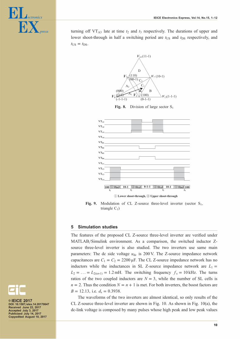
turning off VTA3 late at time t2 and t3 respectively. The durations of upper and
lower shoot-through in half a switching period are tUS and tDS respectively, and
tUS ¼ tDS.
5 Simulation studies
The features of the proposed CL Z-source three-level inverter are verified under
MATLAB/Simulink environment. As a comparison, the switched inductor Z-
source three-level inverter is also studied. The two inverters use same main
parameters: The dc side voltage udc is 200V. The Z-source impedance network
capacitances are C1 ¼ C2 ¼ 2200µF. The CL Z-source impedance network has no
inductors while the inductances in SL Z-source impedance network are L1 ¼L2 ¼ . . . ¼ L2ðnþ1Þ ¼ 1:2mH. The switching frequency fs ¼ 10 kHz. The turns
ratios of the two coupled inductors are N ¼ 3, while the number of SL cells is
n ¼ 2. Thus the condition N ¼ n þ 1 is met. For both inverters, the boost factors are
B ¼ 12:13, i.e. ds ¼ 0:3938.
The waveforms of the two inverters are almost identical, so only results of the
CL Z-source three-level inverter are shown in Fig. 10. As shown in Fig. 10(a), the
dc-link voltage is composed by many pulses whose high peak and low peak values
Fig. 8. Division of large sector S1
Fig. 9. Modulation of CL Z-source three-level inverter (sector S1,triangle C1)
© IEICE 2017DOI: 10.1587/elex.14.20170647Received June 22, 2017Accepted July 3, 2017Publicized July 14, 2017Copyedited August 10, 2017
10
IEICE Electronics Express, Vol.14, No.15, 1–12

are about 2382V and 1191V respectively. According to the given boost factor, the
expected dc-link voltage high peak value is uinH2 ¼ 12:13 � 200 ¼ 2426V. The
difference between the expected value and the actual value (2426V � 2382V ¼44V) is caused by voltage drop across the equivalent resistances, since no closed
loop control is introduced. Fig. 10(b) shows the line voltage before the output
filters. It can be seen that the line voltage amplitude is 2382V. Fig. 10(c) shows the
load phase voltage; its amplitude is about 831V, also a bit smaller than its expected
value 849V (0:7 � 12:13 � 200=2). The simulations results show that the theoret-
ical analysis is correct. The CL Z-source three-level inverter has strong voltage
boosting capability.
6 Conclusions
In this paper, a novel coupled inductor Z-source three-level NPC inverter is studied.
Two coupled inductors are used to replace the two inductors in conventional single
Z-source impedance network. Compare to the single Z-source impedance network,
the proposed inverter has higher boost factor. The novel topology also can achieve
(a)
(b)
(c)
Fig. 10. Simulation results
© IEICE 2017DOI: 10.1587/elex.14.20170647Received June 22, 2017Accepted July 3, 2017Publicized July 14, 2017Copyedited August 10, 2017
11
IEICE Electronics Express, Vol.14, No.15, 1–12
same boost factor as multicell switched inductor Z-source three-level inverter if
N ¼ n þ 1 is satisfied, but its reliability is improved due to the smaller number of
components. SVPWM method for conventional three-level NPC inverter is easy
to apply to the novel inverter with only a slight modification. Simulation results
are provided to verify the features of the proposed topology. For future work,
experimental verification will be carried out.
Acknowledgments
This work was supported by the “Guangdong Provincial Science and Technology
Planning Project of China”, no. 2015A010106015, the “Guangzhou Science and
Technology Planning Project of China”, no. 201607010262, and the “Innovative
Academic Team Project of Guangzhou Education System”, no. 1201610013.
© IEICE 2017DOI: 10.1587/elex.14.20170647Received June 22, 2017Accepted July 3, 2017Publicized July 14, 2017Copyedited August 10, 2017
12
IEICE Electronics Express, Vol.14, No.15, 1–12