a novel three-phase single-switch discontinuous … novel three-phase single-switch...
TRANSCRIPT
160 IEEE TRANSACTIONS ON POWER ELECTRONICS, VOL. 9, NO. 2, MARCH 1994
A Novel Three-phase Single-Switch Discontinuous-Mode AC-DC Buck-Boost
Converter with High-Quality Input Current Waveforms and Isolated Output
Johann W. Kolar, Member-, IEEE, Hans Ertl, Member, IEEE, and Franz C . Zach, Member, IEEE
Abstract-In this paper, a new three-phase single-switch ac-dc flyback converter system is presented. The system operates in the discontinuous mode. The simple structure of its power and control circuit, low mains current distortion, and resistive fundamental behavior, as well as the high-frequency isolation of the controlled output voltage, have to be pointed out. Besides the analysis of the stationary operating behavior, the dependencies of the peak values, average values, and rms values of the device currents, and of the maximum blocking voltages across the power elec- tronic devices on the circuit parameters, are given as analytic approximations. The theoretical analysis is verified by digital simulation.
I. INTRODUCTION HE topic of this paper is the development and analysis of T a circuit concept for the realization of the input unit of a
unidirectional three-phase a c 4 c converter. The converter will be applied as a power supply for an electronic control unit, and will be fed from a 115 V, 400 Hz, three-phase ac system. Due to safety and systems aspects, it has to be realized as a two-stage converter [l]. The controlled output voltage of the rectifier input stage is converted by a d c 4 c converter into the load voltage levels.
The basic development requirements which are relevant for the determination of the concept of the mains converter are defined as follows:
high reliability (low complexity of the power and control
high power density full-load efficiency > 0.85 wide input voltage range isolation of the ac and the dc sides total harmonic distortion factor < 0.05 (with the assump- tion of a purely sinusoidal and symmetric mains voltage system) fundamental displacement factor of the mains current > 0.95
units)
Manuscript received June 25, 1993; revised December 2, 1993. The authors are with the Power Electronics Section 359.5, Technical
IEEE Log Number 9400088. University Vienna, Gusshausstrasse 27, Vienna A-1040. Austria.
current limited start-up, active limitation of the input currents for transient mains overvoltages, limitation of the output current (overload protection) possibility of parallel operation of several converters.
For universal applicability of the ac-dc converter, the dc link voltage is defined as U, = 280V. This is approximately equal to the (ideal) mean output voltage for three-phase diode rectification of the 115 V mains. Due to the high voltage level, this can also be used for buffering of mains voltage outages with relatively low capacitances (minimization of the size). The maximum output power of the mains converter is given by 690 W.
In Section 11, a new topology of a three-phase single-switch pulse rectifier system is developed via a three-phase extension of a d c 4 c flyback converter. Section 111 treats the analysis of the operating principle of the system which forms the basis for the derivation of the equations for the stationary operation (Section IV). With the assumption of high pulse frequency, in Section V analytic approximations of the current stresses (peak values, average values, rms values) on the system components are calculated, and the blocking voltage stresses on the power electronic devices are given. The accuracy (or the limit of applicability) of the analytical approximations is derived via a comparison of the results of the calculations to the results of a digital simulation. Based on Section V, in Section VI the approach for dimensioning the converter is discussed. Furthermore, in this section, the values for the component stresses resulting for the initially given operating parameters are summarized. These component stresses form the basis for the selection of the power electronic devices and can be used in an assessment of the converter within a concept evaluation.
Section VI1 describes a simple extension of the converter structure which leads to an increase of the system efficiency and to a reduction of the blocking voltage stress of the power electronic devices. Finally, the advantages and disadvantages of the converter are compared and commented on in Section VIII.
11. CONVERTER TOPOLOGIES Due to requirements for low effects on the mains and for
high power density, the mains converter has to be realized
0885-8993/94$04.00 0 1994 IEEE
-_._I ~
KOLAR er al.: AC-DC BUCK-BOOST CONVERTER
as a pulse converter system. For high system pulse frequency, the filtering effort is considerably reduced as compared to line- commutated systems [2], [3]. Furthermore, the isolation can be included directly into the converter function and be achieved by a small-size high-frequency transformer.
For the realization of a three-phase pulse rectifier system, one can apply (besides three-phase converter structures) also three single-phase a c 4 c converters which are connected in three-phase configuration [4]-[61.
The combination of three single-phase units makes possible the design of a fault-tolerant system due to the parallel operation (on the output side) of the three partial systems which are fed by the different mains phases. The dimensioning of the three converter modules there has to be performed according to half of the output power of the overall system. This results in a high reliability via the redundancy of one module. Furthermore, the modular design simplifies the system development and test. However, these advantages are paid for by a high device count for power and control circuits, and by a reduction of the power density. A further disadvantage is the basically low utilization of the phase modules, which is due to the instantaneous phase power pulsating with twice the mains frequency. In the case at hand, we prefer a direct three-phase realization.
Based on [7] in [SI-[ 1 11 three-phase unidirectional pulse rectifier systems with high-frequency isolation are introduced. They show a very simple structure of the power and con- trol circuits and satisfy the initially mentioned requirement regarding low system complexity. The converter topologies can be thought to be formed via a three-phase extension of basic dc-dc coverter structures [SI. They are characterized by discontinuous input phase currents (three-phase single-switch discontinuous inductor current mode boost-type rectifier) or by discontinuous input phase voltages (three-phase single-switch discontinuous capacitor voltage mode buck-type rectifier). The mains voltage proportional control of the peak values of the converter input currents/voltages is achieved in analogy to the discontinuous operation of single-phase ac-dc pulse rectifiers (having constant power transistor on-time) directly by the mains voltages/currents (automatic current shaping [ 121). For series connection of a mains filter which suppresses input current harmonics with switching frequency, a considerable reduction of the effects on the mains is achieved, as compared to line-commutated rectification.
As a more detailed analysis of the system behavior shows, the harmonics content of the mains currents remaining after filtering the discontinuous input quantities is essentially de- termined by the voltage or current transformation ratio of the converter [SI, [ 111, [ 131. For example, in three-phase single- switch discontinuous inductor current mode boost rectifier systems, high amplitudes of low-frequency harmonics are present in the mains current spectrum [ 131 for output voltages being low as compared to the amplitude of the line-to-line mains voltage. This leads to a small distortion factor of the mains currents only for high output voltages or for low input voltages, respectively.
Due to the required wide input voltage region, one has to ask the question regarding the topologies of three-phase single-
161
.+I+* + 0 I I I
o!! (d)
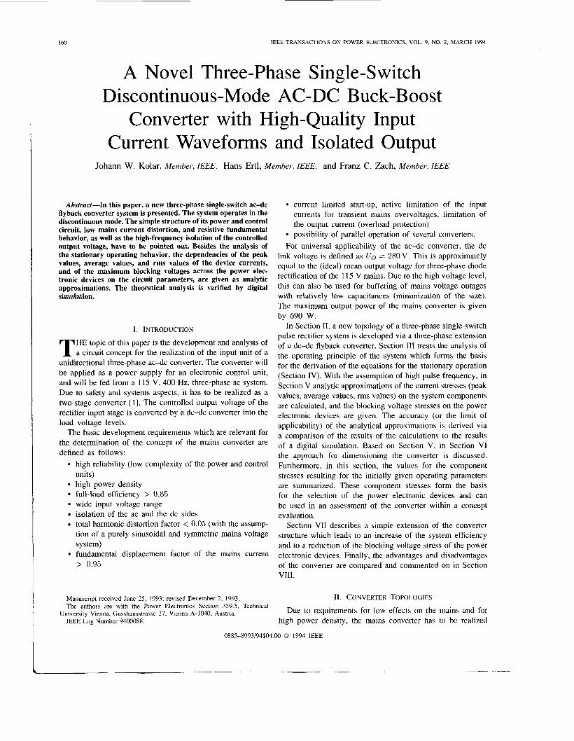
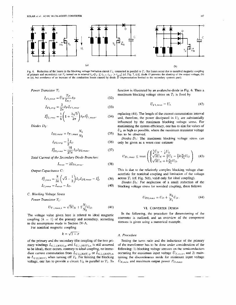
Fig. 1 . Development of three-phase single-switch ac-dc flyback converter topologies (b), (c), (d) based on the basic structure of a dc-dc flyback converter (a). (c) shows the three-phase single-switch discontinuous inductor current mode flyback rectifier (regarding the coupling of the partial windings, cf. Fig. 2).
switch discontinuous-mode pulse rectifier systems with input voltage independent (ideal) sinusoidal input currents.
Discontinuous-mode single-phase ac-dc flyback coverters show a purely sinusoidal shape of the filtered input currents for constant pulse frequency and constant on-time [14]. In connection with the simple structure of the power circuit and the full controllability of the power flow (as given for this converter type), this motivates the development of three-phase pulse rectifier systems based on the basic structure of a dc-dc flyback converter as described in the following.
Fig. l(a) shows the power circuit of a dc-dc flyback con- verter which can be extended to a three-phase converter by connecting a three-phase diode bridge D1 [cf. Fig. l(b)] in series. However, low-frequency harmonics of high amplitude are present in the mains current of this system. This is the case because (due to the operating principle of the three-phase diode bridge) for transistor TI conducting, only two phases conduct current. Therefore, the phase current shape shows 1rI3-wide intervals with zero current.
If one splits up L u , ~ to the valve branches [cf. Fig. l(c)], the mains voltage system and the valve voltage system are decoupled and a simultaneous current flow in all phases is made possible. Due to splitting up the primary windings, the

I62 IEEE TRANSACTIONS ON POWER ELECTRONICS, VOL. 9, NO. 2, MARCH 1994
UN.R I iNL, B L N Fig. 2. Basic structure of the power and control circuits of a three-phase single-switch DICM flyback rectifier; the feeding mains is replaced by a Y-connection of ideal voltage sources u ~ ~ , ( R . s T ) ; filtering of the high-frequency spectral components of the discontinuous converter input currents i ~ ; , l , ~ ~ , ~ ~ ~ by a mains filter L N . Cy. Ro: load resistance (e.g., voltage dependent input impedance of a d c 4 c converter connected to the output of the pulse rectifier). In the stationary case, the control of the power transistor 7'1 is performed by a constant pulse frequency f, and by a constant relative tum-on time bp being set by an output voltage control circuit.
direction of the secondary current is not dependent on the direction of the primary phase currents. The basic secondary circuit structure of the dc-dc converter can therefore be maintained, and the secondary circuits of the phases can be connected in parallel directly.
An ac-side arrangement (and split-up) of L u , ~ results in the converter structure shown in Fig. l(d) 1151 which makes possible [contrary to (c)] a combination of the phase en- ergy storage devices to a three-phase system. For rectifi- cation on the ac currents being present on the secondary, one has to connect the output diodes D2 in a three-phase bridge configuration, however. Therefore, the function of the converter as a flyback converter is linked to a minimum output voltage value defined by mains voltage and turns ratio.
For the case at hand, a closer analysis can therefore be limited to the circuit shown in Fig. l(c), which will be called in the following three-phase single-switch discontinuous inductor current mode (DICM) flyback rectifier.
Remark: If one moves the power transistor TI instead of L V , ~ to the input of the three-phase bridge D1, there follows a three-phase flyback converter structure which requires three turn-off power semiconductor devices. With regard to the desired minimum complexity, this variant (as analyzed in [16]) and other variants of higher complexity (as given in the literature, e.g., in [17], [lS]) will not be considered here.
111. PRINCIPLE OF OPERATION
In analogy to the three-phase single-switch discontinuous- mode pulse rectifier systems, as given in the literature, the control of the system shown in Fig. 2 may be performed in the stationary case with a pulse frequency f p and an on-time of the power transistor TI being constant within the mains period. A synchronization of f p and mains frequency f N is not necessary for f p >> f N . Due to the low-pass characteristic of the mains filter L N , CN, the mains voltage can be assumed to lie directly at the filter output.
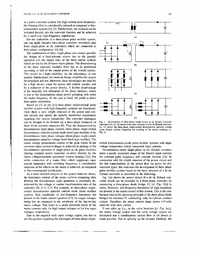
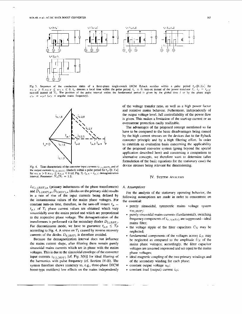
For illustrating the operating principle, Fig. 3 shows the conducting states of the converter occurring during the pulse period t , E [0, Tp]. ( t , denotes a local time running within the considered pulse period.) Concerning the mains phase voltages being approximately constant within the pulse period, we as- sume U N , R > 0, UN,T < U N , ~ < 0 (being valid in an interval of 7r/6 of the mains fundamental period [cf. Fig. 5(a)]). Due to the phase-symmetric structure of the converter and due to the assumption of a purely sinusoidal voltage system, the analysis of this angle interval determines the system behavior within the entire fundamental period. Fig. 4 shows the local shape of the phase currents being related to Fig. 3.
Before tuming on T I , we have, according to the oper- ation of the system in discontinuous mode, Z U , I , ( R S T ) = iU,2,(RST) = 0. TI is turned on at t,, = 0. The dc side short-circuit of the bridge circuit consisting of L L T , ~ , ( R S T ) , ~ =
KOLAR et al.: AC-DC BUCK-BOOST CONVERTER 163
Fig. 3. Sequence of the conduction states of a three-phase single-switch DICM flyback rectifier within a pulse period t , , f [ O . Tp] for tijLr.R > 0. ZI,V.T 5 7t:v.s 5 0. t,, denotes a local time within the pulse period. t,, = 0: tum-on instant of the power transistor T I . t,, = t , , , ~ : tum-off instant of TI. The position of the pulse interval within the fundamental period is given by the global time t or by the phase angle 9.v = d,vt (djv = angular mains frequency).
t,= -I TP
IU,l,T ' U Fig. 4. Time characteristic of the converter input currents Z U , ~ , ( R S T ) and of the output currents ~ ~ T , ~ , ( R s T ) (dashed) within a pulse period for t P e [ O , Tp] for ~ L X , R > O,u.iv,t 5 u ~ , s 5 0 (cf. Fig. 3). t P , 4 - t P , l : demagnetization interval. Parameter: iV2/N1 = 1.2.
LU, l , (RST) ,n (primary inductances of the phase transformers) and D ~ , ( R s T ) , ~ , D ~ ( R s T ) , ~ (diodes on the primary side) results in a rate of rise of the input currents being defined by the instantaneous values of the mains phase voltages. For constant tum-on time, therefore, in the tum-off instant t , = t,,l of TI phase current values are obtained which vary sinusoidally over the mains period and which are proprotional to the respective phase voltage. The demagnetization of the transformers is performed via the secondary diodes Dz,(RsT). For discontinuous mode, we have to guarantee t , ) 4 5 T p according to Fig. 4. A stress on TI caused by reverse recovery currents of the diodes D z , ( R s ~ ) is therefore avoided.
Because the demagnetization interval does not influence the mains current shape, after filtering there remain purely sinusoidal mains currents which are in phase with the mains voltages. This is due to the sinusoidal envelope of the converter input currents iU,l ,(RST) [cf. Fig. 5(b)] for ideal filtering of the harmonics with pulse frequency (cf. Section IV-B). The system therefore shows (contrary to, e.g., three-phase DICM boost-type rectifiers) low effects on the mains independently
of the voltage transfer ratio, as well as a high power factor and resistive mains behavior. Futhermore, independently of the output voltage level, full controllability of the power flow is given. This makes a limitation of the start-up current or an overcurrent protection easily realizable.
The advantages of the proposed concept mentioned so far have to be compared to the basic disadvantages being caused by the high current stresses on the devices due to the flyback converter principle and by a high filtering effort. In order to establish an evaluation basis conceming the applicability of the proposed converter system (going beyond the special application described here) and conceming a comparison to altemative concepts, we therefore want to determine (after formulation of the basic equations for the stationary case) the device stresses being relevant for dimensioning.
Iv . SYSTEM ANALYSIS
A. Assumptions
For the analysis of the stationary operating behavior, the following assumptions are made in order to concentrate on the essential:
purely sinusoidal, symmethc mains voltage system ' U . N , ( R S T ) ;
purely sinusoidal mains currents (fundamental), switching frequency components of ~ u , ~ ( ~ s ~ ) are suppressed-ideal mains filter; the voltage ripple of the filter capacitors CN may be neglected; fundamental components of the voltages across LN may be neglected as compared to the amplitude UN of the mains phase voltages; accordingly, the filter capacitor voltages are assumed impressed and set equal to the mains phase voltages; ideal magnetic coupling of the two primary windings and of the secondary winding for each phase; constant output voltage U O ; constant load (output) current io;
IEEE TRANSACTIONS ON POWER ELECTRONICS, VOL. 9, NO. 2, MARCH 1994
I I I
(b)
I I I I I
I I I 1
(e)
2 "T1
I I I I I (C)
I I 1 I I I I I I I
( f )
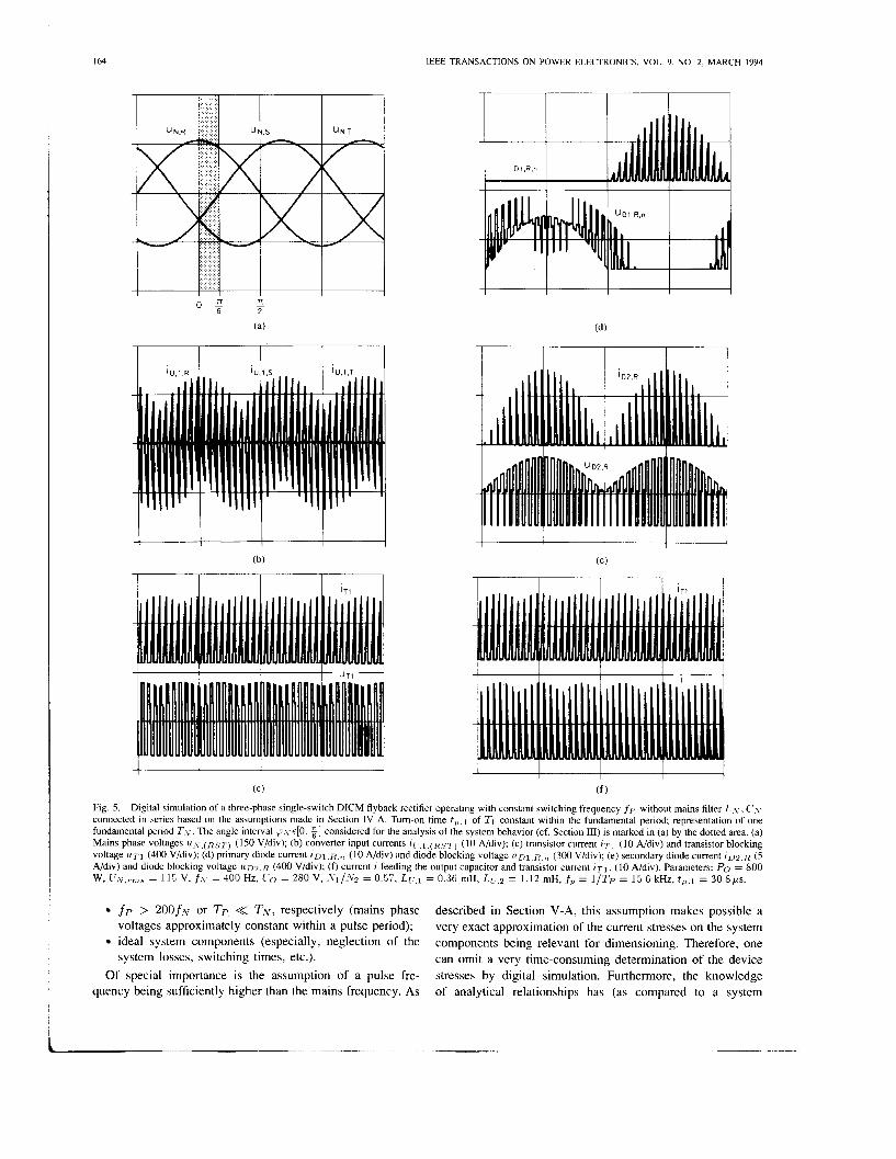
Fig. 5. Digital simulation of a three-phase single-switch DICM flyback rectifier operating with constant switching frequency fp without mains filter L:,-. C.y connected in series based on the assumptions made in Section IV-A. Tum-on time f f , , l of TI constant within the fundamental period; representation of one fundamental period T.Y. The angle interval +.yf[O. :] considered for the analysis of the system behavior (cf. Section 111) is marked in (a) by the dotted area. (a) Mains phase voltages I ( . ~ , ( R ~ T ) (150 V/div); (b) converter input currents i c - , l , ( ~ , ? ~ ) ( I O A/div); (c) transistor current i ~ 1 (10 A/div) and transistor blocking voltage it^^ (400 V/div); (d) primary diode current i ~ l , ~ , , , (10 A/div) and diode blocking voltage i (D1 ,R , r , (300 V/div); (e) secondary diode current i ~ z . ~ (5 A/div) and diode blocking voltage I I D Z . R (400 V/div); (0 current i feeding the output capacitor and transistor current i r l , (10 A/div). Parameters: Po = 800 W, C7!v ,,., I 1 c = 115 V, f . ~ = 400 Hz, C-0 = 280 V, Sl/.Vz = 0.57, L c . . ~ = 0.3G mH, L[; .2 = 1.12 mH, f, = 1 / T p = 15.G kHz, t i , , ] = 30.8ps.
f p > 2 0 0 f N or T p << TIL., respectively (mains phase voltages approximately constant within a pulse period); ideal system components (especially, neglection of the system losses, switching times, etc.).
Of special importance is the assumption of a pulse fre- quency being sufficiently higher than the mains frequency. As
described in Section V-A, this assumption makes possible a very exact approximation of the current stresses on the system components being relevant for dimensioning. Therefore, one can omit a very time-consuming determination of the device stresses by digital simulation. Furthermore, the knowledge of analytical relationships has (as compared to a system

KOLAR er al.: AC-DC BUCK-BOOST CONVERTER
analysis by digital simulation whose validity is limited to discrete parameter sets) the advantage of a deeper insight into the system behavior, and therefore allows an immediate conclusion regarding the influence of parameter variations on the device stresses.
B. Basic Equations The analysis of the basic equations of the stationary oper-
ating mode is performed for constant f p and constant local on-time t,,1 of TI . Furthermore, only the discontinuous mode is assumed as well as a symmetric split-up of the primary windings of the transformers according to
(1)
For the relation of primary and secondary inductances, we have
L U , l , ( R S T ) , , = L U , l , ( R S T ) , , = LU, l .
according to the assumption of ideal coupling. Based on a symmetrical, purely sinusoidal mains voltage system
U N , R = UN COS ( ( P N )
(3)
there follows for the instantaneous input phase currents at tum-off instant of TI t , = t,,1 (cf. Fig. 4)
There, the position of the considered pulse interval within the fundamental period TN is defined by the angle
(PN = w N t . ( 5 )
The mains currents remaining after (ideal) filtering of the spectral components with pulse frequency (cf. L N , CN in Fig. 2) of the discontinuous input currents z U , l , ( R S T ) now follow directly via averaging related to the pulse period as
where 1
6 P = -t,,1 T P
(7)
denotes the relative tum-on time or the duty cycle of the power transistor TI . As already described in Section 111, no
165
low-frequency effects of the system on the mains occur. The amplitude of the (ideally) purely sinusoidal mains currents being in phase with the mains phase voltages is given with (6) as
.. 1 - Tp 2 IN = -U,-Sp.
2 L U , l
Regarding the loading of the mains, the converter therefore can be assumed to be replaced by equivalent resistances
(9)
(for Y-connection) which can be set by the relative tum-on time Sp of TI.
Remark: This defining equation of an input-equivalent resis- tance is also given in an identical form for DICM dc-dc (cf. eq. (13) in [19]) and for single-phase ac-dc flyback converters (cf. eq. (13.28) in [12]) and is valid approximately also for three- phase single-switch DICM boost-type input rectifiers (cf. eq. (16) in [8] or eq. (38) in [13]).
Considering the equality of input and output power (because the system has been assumed loss-free), we have the converter output power
3 - T P 2 Po = -Ui-hp. 4 L U J
For ideal magnetic coupling and for discontinuous operation, the entire magnetic energy being stored at instant t , = t,,1
in the primary inductances is transferred into the secondary within each pulse period. The power flow as averaged over one pulse period is therefore not influenced by the value of the output voltage U O , and has the time-constant value
for the stationary case. The system shows a constant-power behavior on the output side being also characteristic for single- phase ac-dc flyback converters operating in discontinuous mode [20]. One has to point out, however, that in the case at hand (contrary to single-phase systems) also for highly dynamic output voltage control no low-frequency distortion of the input current shape occurs. This is due to the time-constant (average) power flow for constant tum-on time.
As shown in the following section, besides the output current
PO Io = - U0
and the duty ratio 6 p of T I , the global maximum value of the transistor current
and the global maximum value of the output diode current
Nl N 2
I D 2 , m a x = I T 1 , m a x -
are of paramount importance regarding the current stress on the system components.

I66 IEEE TRANSACTIONS ON POWER ELECTRONICS, VOL. 9, NO. 2, MARCH 1994
Remark: In this paper, a global maximum value denotes the maximum of a signal characteristic within the fundamental period. This maximum value has to be distinguished from a local maximum value being present within a pulse interval; e.g., the current values Z U , ~ , ~ , ~ , ( R S T ) given in (4) represent local maximum values of the input current shape.
For the relation of the amplitude of the mains current fundamental and the maximum transistor current, there follows with (8) and (13)
Therefore, the results, e.g., for Sp = 0.5, a current stress on TI being four times the peak value of the mains current fundamental. This clearly points out the high current stress on the devices characterizing the discontinuous mode of a flyback converter.
For the (global) maximum duration of the current flow within a pulse interval, there follows
0 6 ) where
denotes the maximum duration of the demagnetization phase. For discontinuous mode, we therefore have to guarantee
V. COMPONENT RATINGS For dimensioning and determination of the application re-
gion of the system, the current and voltage stresses on the power electronic devices, as well as on the passive com- ponents, are of special interest. The current and voltage characteristics to be analyzed for the calculation of the com- ponent stresses are shown in Fig. 5(c)-(f), with the exception of the mains filter and the output capacitor currents.
The calculation of the dependencies of device stresses being relevant for dimensioning (current and blocking voltage peak values, current average, and rms values) on the system parameters (input voltage, output voltage, output power, tums ratio, pulse frequency, etc.) as simple analytic approximations is the topic of the following subsections.
A. Analysis Method The basis of the calculation method is a quasi-continuous
analytical approximation of the discontinuous behavior [2 11, [22], being defined by averaging the quantities over a pulse period. The knowledge of the characteristic of a time function ii(t,) within one pulse period t , E [0, Tp] is replaced there by the (discrete) quantities, which can be denoted as local mean value
and local rms value TP
i:(t,)dt,.
(Remark: The local rms value corresponds to a discrete time function having equal loss.) If these local mean values now are related to the postion p~ of the pulse interval within the fundamental period TN (or to the global time t = w ; " ~ N ) , then there is defined a continuous (global) time characteristic of the local mean value and of the local rms value. By a second averaging related to the fundamental period.
there follow accordingly and directly the quantities global mean value and global rms value which characterize the component stresses.
In connection with a minimization of component size and weight of the magnetic devices, one has to aim in a prac- tical realization, by all means, for f p >> f ~ . As a digital simulation based on the assumptions made in Section IV-A shows, the deviations of the analytical expressions from exact results remain below 2% for f p > 2 0 0 f N . Because in the discontinuous mode a transistor stress by reverse recovery currents of the output diodes 0 2 is avoided, f p = 5 0 0 f ~ seems to be obtainable in the case at hand. Therefore, the analytical approximations (2 1) and (22) show high accuracy. The computation results given in the following can therefore be applied directly as the basis for dimensioning.
B . Characteristic Current Values of the Devices Mains Filter Capacitance CN:
Secondary:
Diodes DI:
__ __ . .
0
T2
UL
0 J STl C'TI
Power Transistor TI
.. T P
L U J I T 1 , m a x = U N - b P
3 2a IT1,avg = - b P I T l , m a x
n - D
& C =L, -= --I ST2
-0
Diodes D2:
Total Current of the Secondary Diode Branches:
I m a x = 2 I D 2 , m a z .
Output Capacitance C:
C. Blocking Voltage Stress
Power Transistor TI : Nl N2
U T l , m a x , i = h O N 2-UO.
function is illustrated by an avalanche-diode in Fig. 6. Then a maximum blocking voltage stress on TI is fixed by
(32)
replacing (41). The length of the current commutation interval and, therefore, the power dissipated in UL are substantially influenced by the maximum blocking voltage stress. For maximizing the system efficiency, one has to aim for values of UL as high as possible, where the maximum transistor voltage
Diodes D 1 : The maximum blocking voltage stress can
(34)
(35) has to be observed.
(36) only be given as a worst-case estimate
This is due to the relatively complex blocking voltage char- acteristic for nonideal coupling and limitation of the voltage across TI (cf. Fig. 5(d), valid only for ideal coupling).
Diodes D2: For neglection of a small reduction of the blocking voltage stress for nonideal coupling, there follows
(39)
(40)
The voltage value given here is related to ideal magnetic coupling ( I C = 1) of the primary and secondary, according to the assumptions made in Section IV-A.
For nonideal magnetic coupling
IC=G
of the primary and the secondary (the coupling of the two pri- mary windings L u , ~ , ( R s T ) , ~ and L U , ~ , ( R ~ T ) , ~ is still assumed to be ideal), there occurs, contrary to ideal coupling, no imme- diate current commutation from L u , ~ , ( R s T ) , ~ or L u , ~ , ( R s T ) , ~ to L U , z , ( R S T ) when turning off TI . For limiting the blocking voltage, one has to provide a circuit UL in parallel to TI . Its
(41) VI. CONVERTER DESIGN
In the following, the procedure for dimensioning of the converter is outlined, and an overview of the component stresses is given using a numerical example.
A. Procedure
Setting the turns ratio and the inductance of the primary of the transformer has to be done under consideration of the following: 1) blocking voltage stresses on the semiconductors occumng for maximum input voltage UN,,,,, and 2) main- taining the discontinuous mode for minimum input voltage U N , ~ ~ ~ and maximum output power Po,,,,.
168 IEEE TRANSAmIONS ON POWER ELECTRONICS, VOL. 9, NO. 2, MARCH 1994
I IU.1.R ,
IU.2.R
'U.2.T Iu.2.s
Iu.1.s
IU.1.T
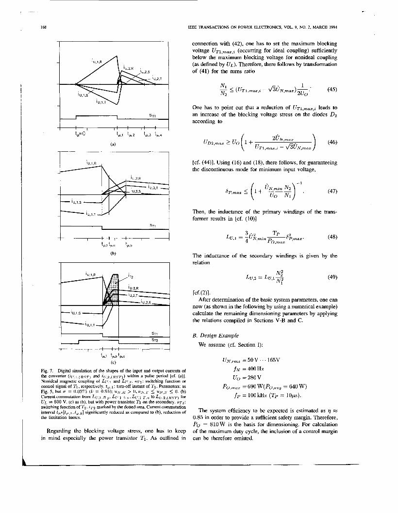
Fig. 7. Digital simulation of the shapes of the input and output currents of the converter ( i [ r , l , ( ~ ~ ~ ) and ~ ( ; , ~ , ( R , S T ) ) within a pulse period [cf. (a)]. Nonideal magnetic coupling of L[;.I and Lii.2. ST^: switching function or control signal of T I , respectively. t,, , I : turn-off instant of TI . Parameters: as Fig. 5, but o = 0.0975 (I; = 0.95); P L ~ V , R > O , I L ~ V . T 5 U N , S 5 0. (b) Current commutation from L ~ ~ . ~ . R . ~ , L ~ ~ , ~ . , ~ , , , , L ~ ~ . ~ . T , . ~ toLCr,2,(RST) for
= SO0 V. (c) as (b), but with power transistor Tz on the secondary. ST^: switching function of T2, i ~ 2 marked by the dotted area. Current commutation interval t , , c [ t l , , l , t , , b ] significantly reduced as compared to (b), reduction of the limitation losses.
Regarding the blocking voltage stress, one has to keep in mind especially the power transistor TI. As outlined in
connection with (42), one has to set the maximum blocking voltage (occurring for ideal coupling) sufficiently below the maximum blocking voltage for nonideal coupling (as defined by U,). Therefore, there follows by transformation of (41) for the tums ratio
One has to point out that a reduction of leads to an increase of the blocking voltage stress on the diodes 0 2
according to
[cf. (44)l. Using (16) and (18), there follows, for guaranteeing the discontinuous mode for minimum input voltage,
Then, the inductance of the primary windings of the trans- former results in [cf. (lo)]
The inductance of the secondary windings is given by the relation
[cf.(2)1. After determination of the basic system parameters, one can
now (as shown in the following by using a numerical example) calculate the remaining dimensioning parameters by applying the relations compiled in Sections V-B and C.
B . Design Example We assume (cf. Section I):
UN,,,, = 50 V . . .165V f~ = 400 HZ U0 = 280 V
P0,max = 690 W(P0,avg = 640 W ) f p = 100 kHz (Tp = lops).
The system efficiency to be expected is estimated as 7 M 0.85 in order to provide a sufficient safety margin. Therefore, PO = 810 W is the basis for dimensioning, For calculation of the maximum duty cycle, the inclusion of a control margin can be therefore omitted.

KOLAR et al.: AC-DC BUCK-BOOST CONVERTER
For the threshold level of the blocking voltage limitation circuit (which defines the maximum blocking voltage of TI) , we choose
U, = 800V
and
U T l , m a x , i = 600v .
This is done considering the actually occumng blocking voltage stress which should be well below the maximum allowable blocking voltage.
U T 1 , m a x 5 1000v
(for guaranteeing high operation reliability) for the MOSFET's which are used in parallel for the realization of 7'1.
An altemate realization of the switch can be realized par- alleling a power MOSFET and an IGBT. This allows a minimization of the conduction and switching losses with a low circuit and control effort [23]. In this case, also, the given assessements conceming the blocking voltage stress are still valid.
The leakage of the transformer is estimated as
U = 0.025.
According to Sections VI-A and V-C, there follows, then,
As already mentioned in Section IV-B, the component cur- rent stress is essentially determined by the maximum values of the transistor current and the output diode current, and by the duty ratio Sp. For the determination of the maximum stress on the ac-side components, one therefore has to consider the case of minimum input voltage (or maximum Sp, respectively).
Remark: Because the output power is determined directly by the maximum value of the transistor current according to
[cf. (10) and (13)], for constant output power IT^,^^, and, therefore, the secondary currents are not influenced by the input voltage value. The current characteristic values of the dc-side devices are therefore only dependent on the output power and not on the input voltage.
I69
By evaluating the relations given in Sections IV-B and V-B,
Amplitude of the Mains Current Fundamental: we get the following current ratings.
IN,,,, = 7.6 A.
Mains Filter Capacitor CN:
I C N , r m s = 6.2 A I c N , ~ , , = 19.0 A.
Transformer Inductances L u , ~ , ~ , L u , ~ , , , L u , ~ : Primary:
I u , l , p , m a x = I U , l , n , m a x = 26.6 A I U , l , p , r m s = I U , l , n , r m s = 5.9 A.
Secondary:
I ~ , ~ , m a x = 9.3 A I ~ , 2 , r m s = 2.3A.
Diodes Dl :
ID^,^^, = 26.6 A
I D 1 , a v g = 2.5 A = 5.9 A.
Power Transistor TI :
IT^,^,, = 26.6 A
I T l , a v g = 7.4 A IT^,^,^ = 11.2 A.
Diodes D 2 :
I D 2 , m a x = 9.3 A ID2 ,avg = 0.96 A
I D 2 , r m s = 2.3 A.
Total Current Through Diodes D 2 :
I,,, = 18.6 A.
Output Capacitor C:
I C , ~ , ~ = 4.9A I C , ~ , ~ = 15.7 A.
Output Current IO:
I o = 2.9A.

I70 IEEE TRANSACTIONS ON POWER ELECTRONICS, VOL. 9, NO. 2, MARCH 1994
VII. EFFIENCY IMPROVEMENT
As mentioned in Section V-C, and as easily verifiable by digital simultion, the obtainable efficiency is influenced substantially by the difference UL - U ~ l , ~ ~ ~ , i , as well as by the loss contributions of the semiconductors and the passive components. A high efficiency is inevitably linked to a high blocking voltage stress on TI (defined by U L ) and to low tranformer leakage (connected with a high manufacturing effort).
A fictitious increase of UL (while avoiding an increase of the blocking voltage stress on T I ) can now be achieved by applying a second power transistor T2 (on the secondary) and of an output diode D (cf. Fig. 6, left side). T2 is turned on in the interval between turn-on instant and turn-off instant of TI [cf. Fig. 7(c)J. During the conduction period of T I , a current flow via T2 is suppressed by the fact that the output diodes [cf. Fig. 6(a)] are in the blocking state, or by the diodes D being connected in series to T2 [cf. Fig. 6(b)]. By shorting the secondary winding, the transformatory coupling of a voltage into the primary (which would slow down the current commutation) is suppressed. Due to this, the current commutation interval is shortened, and the losses in U, are reduced accordingly.
After turning off T2, the magnetization energy (stored in LU,P,(RST)) is fed into the output via diode D which prevents shorting of the output voltage when T2 is turned on. Due to its very short on-time, one has to dimension T2 regarding the pulse current stress, and a transistor with low average current carrying capability can be applied. The control of T2, which is directly linked to the turn-off of TI , furthermore allows a simple realization of the control stage. Therefore, with a small increase of system complexity, a significant converter efficiency improvement (or a reduction of the blocking voltage stress in TI , respectively) is made possible.
VIII. CONCLUSIONS
Based on the topology of a dc-dc flyback converter, a new three-phase single-switch DICM rectifier system has been developed in this paper.
The system is characterized by the following advantages and disadvantages.
+ Ideally, there is complete avoidance of low-frequency effects on the mains (purely sinusoidal mains currents being in phase with the mains voltages). Simple structure of the power circuit and of the control circuit (constant pulse frequency and-for the stationary case-constant tum-on time of the power transistor allow the application of standard SMPS control IC's), possibility of sensing the output voltage to be controlled by a third transformer winding which also can be used for the internal supply of the system.
+
High-frequency potential separation between ac and dc sides (possibility of matching the input and output voltage levels and reduction of the component stress by proper choice of the turns ratio). Simple control behavior-corresponds to a DCIM dc-dc flyback system [24], [25] due to the time-constant average power flow [cf. (1 1)l. full controllability of the power flow [inrush-current limitation (start-up or transient over-voltages of the mains), output current limitation (load faults)]. Low circuit effort when various potential separated output voltages are to be realized. Possibility of direct parallel operation of several converters. High peak current stress on the components (high conduction losses, especially if a power MOSFET is used for realizing 2'1, high requirements regarding the ESR (equivalent series resistance) of the filtering and smoothing capacitors, etc.. High blocking voltage stress on the power semiconductors. Low utilization of the magnetic cores; transfer of power pulsating with twice the mains frequency; relatively low utilization of the primary winding by splitting it up into two partial windings where each conducts only one current half-wave per mains period; unidirectional (unsymmetric) magnetization of the transformers. High filtering effort for avoiding conducted EM1 (electromagnetic interference)-reduction of the power density of the system.
The advantages and drawbacks mentioned above corre- spond, to a large extent, to those of a DICM dc-dc flyback converter; an application of the system is especially of interest for low output power (< 1 kW) and low rated mains voltage. Finally, it shall be pointed out that one can basically avoid low- frequency effects on the mains only for the discontinuous mode of the system (when three-phase energy is transformed into dc energy, and only a single controlled power electronic device is used). The high current stress being paid for the simple system structure therefore (contrary to dc-dc converters) cannot be reduced by choosin-g the continuous mode.
APPENDIX LIST OF SYMBOLS
C C N D
D1 D2
fP fN
i
iC
Output capacitor. Mains filter capacitor. Blocking diode on the secondary side. Diodes on the primary side. Diodes on the secondary side. Mains frequency. Pulse frequency. Total current of the three secondary branches. Output capacitor current.

KOLAR et al.: AC-DC BUCK-BOOST CONVERTER 171
i C N
iD1
iD2
PO RN
t
T
Tl T2
U T l , m a x , i
‘PN
Current through the capacitors of the mains filter. Current through D1 (primary side). Current through Dz (secondary side). Mains phase currents. Current through transistor TI. Input phase currents. Primary currents of the transformers (positive branches). Primary currents of the transformers (negative branches) . Transformer secondary currents. Coupling factor between primary and secondary windings. Mains filter inductances. Inductance of a primary winding (positive or negative branch). Inductance of a secondary winding. Number of tums of a primary winding. Number of tums of a secondary winding. Output power. Power-equivalent input resistance of the converter (Y-connection). (Global) time (within a fundamental period). Global maximum value of the sum of tum-on time of TI and duration of the demagnetization phase. Main power transistor. Auxiliary power transistor for reduction of the losses in UL. Mains fundamental period. Pulse period. Microscopic (local) time counted within a pulse interval. Threshold voltage of the voltage limitation circuit of TI. Mains phase voltages. DC output voltage. Maximum blocking voltage stress on TI for nonideal magnetic coupling. Maximum blocking voltage stress on TI for ideal magnetic coupling. Relative tum-on time of TI , duty cycle. Phase assigned to time
fundamental period. t(cpN = WNt) within the
Mains angular frequency. Transformer leakage coefficient (according to coupling k) .
Lower case letters characterize (local or global) time-dependent quantities. Upper case letters characterize time-indpendent global mean or rms values.
Indices:
aug i
max min n
P
(RST)
tpz rms
P 1 2
linear mean value common counting subscript, ideal magnetic coupling global maximum value global minimum value components between the phase inputs and the negative bus bar of the primary bridge components between the phase inputs and the positive bus bar of the primary bridge phase R or phase S or phase T quadratic mean value time assignment of local current value local time (within a pulse period) primary side secondary side
ACKNOWLEDGMENT
The authors are very much indebted to the Austrian Fonds zur Forderung der wissenschalftlichen Forschung, which sup- ports the work of the Power Electronics Section at their university.
REFERENCES
[ I ] B. Carpenter, R. Lewis, B. Choi, B. Cho, and F. C. Lee, “A distributed power system for military VLSI applications,” in Proc. IEEE HFPC Conf., San Diego, CA, May 1-5, 1988, pp. 430-441.
[2] E. K a ” , “New military EM1 specifications affecting the input circuit architecture of ac to dc converters,” in Proc. 8th Int. Solid-State Power Electron. Conf., Dallas, TX, Apr. 27-30, 1981, pp. C-3 1-11.
[3] B. K. Bose, “Recent advances in power electronics,” IEEE Trans. Power Electron., vol. 7, pp. 2-16, 1992.
[4] M. J. Kocher and R. L. Steigenvald, “An ac-to-dc converter with high- quality input waveforms,” IEEE Trans. Ind. Appl., vol. IA-19, pp. 586599, 1983.
[ 5 ] R. A. Langley, J. D. Van Wyk, and J. J. Schoeman, “A high-technology battery charging system for railway signalling applications,” in Proc. 3rd Europ. Conf. Power Electron. Appl., vol. 3, Aachen, Oct. 9-12, 1989, pp. 1433-1437.
161 F. C. Lee, D. BorojeviC, and V. VlatkoviC, “Three-phase power factor correction circuits-Topologies and control,” in Proc. 10th Annu. Power Electron. Seminar, Tutorial 1-2, Blacksburg, Sept. 20-22, 1992, pp. 75-123.
[7] A. R. Prasad, P. D. Ziogas, and S. Manias, “An active power factor correction technique for three-phase diode rectifiers,” IEEE Trans. Power Elecrron., vol. 6, pp. 83-92, 1991.
[8] E. Ismail and R. W. Erickson, “A single transistor three-phase resonant switch for high-quality rectification,” in Conf. Rec. 23rd Power Electron. Special. Conf., vol. 11, Madrid, June 29-July 3, 1992, pp. 1341-1351.
[9] J. Pforr and L. Hobson, “A novel power factor-corrected single-ended resonant converter with three-phase supply,” in Conf. Rec. 23rd Power Electron. Special. Conf., vol. 111, Madrid, June 29-July 3, 1992, pp. 1368-1 375.

I72 IEEE TRANSACTIONS ON POWER ELECTRONICS, VOL. 9. NO. 2 , MARCH 1994
[lo] L. Malesani, L Rossetto, G. Spiazzi, P Tenti, I. Toigo, and F Dal Johann W. Kolar (M’89) was born in Upper Aus- Lago, “Single-switch three-phase ac-dc converter with high power factor tna on July 15, 1959 He is currently working and wide regulation capability,” in Pioc 14th Int Telecommun Energ) toward the Ph D. degree in the area of analysis and Conf , Washington, DC, Oct 4-8, 1992, pp. 279-285 control optimization of single-phase and three-phase
[ l I] J W Kolar, H. E d , and F C Zach, “Power quality improvement of PWM rectifier systems. three-phase ac-dc power conversion by discontinuous mode ‘Dither’. He is with the Power Electronics Section of the rectifiers,” in Proc 6th Powei Qualib Conf. Munich, Oct 14-15. Technical University of Vienna, and he is involved 1992, pp 62-78 as a consultant in several industnal research and
[12] S D Freeland, “Input current shaping for single-phase ac-dc power development projects on switched-mode power sup- converters,” Ph.D dissertation, Part 11, Calif. Inst. Technol., Pasadena, plies He also does research in the areas of inverter 1988 and converter development and of theoretical anal-
t131 J. w Ertl, and Zach, “SPace vector-based ysis of all kinds of power electronic systems. He is the author of numerous analysis of the input current distortion of a three-phase discontinuous- technical and mode boost rectifier In conf 24th IEEE Mr. Kolar received the award of the Power Systems Engineering Society Special Conf , Seattle, WA, June 2G24, 1993, pp. 696-703. (OGE) of the Austnan Institute of Electncal Engineers (OVE) for his research
“Dynamic power factor correction In on the minimization of the mains current distortion of three-phase a c 4 c capacitor input off-line converters,” in Pioc 6th Nut Solid-State Power Conversion Conf, Miami Beach, FL, May 2 4 , 1979, pp B-3 1-6.
[IS] J. W Kolar, H Ertl, and F C Zach, “Analysis and design of a new three-phase power conditioner providing sinwoidal input currents and multiple isolated dc outputs,” in Pioc 26th Int Power Conversion Conf , Nurnberg, Germany, June 21-24, 1993, pp 151-165.
[I61 R. Itoh and K Ishizaka, “Three-phase flyback ac-dc converter with sinusoidal supply currents,” IEE Proc B , vol 138, pp 143-151, 1991.
1171 S. Manias, A. R. Prasad, and P. D. Ziogas, “A 3-phase inductor fed SMR converter with high frequency isolation, high power density and improved power factor,” in Conf Rec IEEE Ind Appl Annu Meet , Pt. I, Atlanta, GA, Oct 18-23, 1987, pp. 253-263
1181 T Aoki, S Muroyama, and M Igararhl, “A new switched-mode rectifier with sinusoidal input current waveforms,” in Pioc Power Election Conf , vol 2, Tokyo, Apr 2 4 , 1990, pp. 755-760
[I91 S. Singer and R W Enckson, “Canonical modeling of power processing circuits based on the POP1 concept,” IEEE Trans Power Election , vol. 7, pp 3 7 4 3 , 1992
[20] R. Enckson, M Madigan, and S Singer, “Design of a simple high- power-factor rectifier based on the flyback converter,” in Conf Rec 5th Appl Power Election Conf , Los Angeles, CA, Mar. 11-16, 1990, pp
papers and patents
[14] D. Chambers and systems In 1993
Hans Ertl (M’93) was bom in Upper Austria on May 28, 1957. He received the Dip1 Ing. (M.Sc.) de- gree from the Technical University Vienna, Austna, in 1984 As a Scientific Assistant of the Power Elec- tronics Section, he has recently finished the Ph D thesis in the area of three-phase PWM converter systems.
He also does research concerning the analysis and design of switched mode power supplies He is the author of various technical and scientific papers and patents.
792-801. 121) J. W. Kolar, H. Ertl, and F. C. Zach, “Calculation of the passive and
active component stress of three-phase PWM converter systems with high pulse rate,” in Proc. 3rd Euro. Conf. Power Electron. Appl., vol. 3, Aachen, Oct. 9-12, 1989, pp. 1303-1311.
[22] R. Redl and L. Balogh, “RMS, DC, peak, and high-frequency power- factor correctors with capacitive energy storage,” in Proc. 7th Appl. Power Electron. Conf., Boston, MA, Feb. 23-27, 1992, pp. 533-540.
[23] Y. M. Jiang, G. C. Hua, E. X. Yang, and F. C. Lee, “Soft-switching of IGBTs with the help of MOSFETs,” in Proc. 10th Annu. VPEC Power Electron. Seminar, Blacksburg, VA, Sept. 20-22, 1992, pp. 77-84.
[24] S. Cuk and R. D. Middlebrook, “A general unified approach to modelling switching Dc-to-Dc converters in discontinuous conduction mode,” in Conf. Rec. IEEE Power Electron. Special. Conf., Palo Alto, CA, June 14-16, 1977, pp. 3 6 5 7 .
[25] A. S. Kislovski, R. Redl, and N. 0. Sokal, Dynamic Analysis of Switching-Mode Dc-Dc Converters. New York: Van Nostrand Rein- hold, 1991.
Franz C. Zach (M’82) was bom in Vienna, Austna, on December 5 , 1942. He received the DipLIng. (M.Sc.) and Ph.D degrees (cum laude) from the University of Technology, Vienna, Austna, in 1965 and 1968, respectively
From 1965 to 1969 he was a Scientific Assistant in Vienna; and from 1969 to 1972, he was with the NASA Goddard Space Flight Center in Greenbelt, MD (Washington, DC). In 1972 he retumed to Austna to become Associate Professor for Power Electronics at the Vienna University of Technology,
where he has been heading the Power Electronics Section since 1974. He is the author of numerous technical and scientific papers and patents and of two books on automatic control and power electronics His current activities lie in power electronics and associated controls, especially as used for variable- speed ac and dc motor dnves and for power supplies He is also involved in extensive industrial work in these areas.