a novel variation-tolerant 9t sram design for nanoscale cmos
TRANSCRIPT

Rochester Institute of TechnologyRIT Scholar Works
Theses Thesis/Dissertation Collections
5-1-2010
A Novel variation-tolerant 9T SRAM design fornanoscale CMOSSreeharsha Tavva
Follow this and additional works at: http://scholarworks.rit.edu/theses
This Thesis is brought to you for free and open access by the Thesis/Dissertation Collections at RIT Scholar Works. It has been accepted for inclusionin Theses by an authorized administrator of RIT Scholar Works. For more information, please contact [email protected].
Recommended CitationTavva, Sreeharsha, "A Novel variation-tolerant 9T SRAM design for nanoscale CMOS" (2010). Thesis. Rochester Institute ofTechnology. Accessed from
A Novel Variation-Tolerant 9T SRAM Design for
Nanoscale CMOS
by
Sreeharsha Tavva
A Thesis Submitted in Partial Fulfillment of the Requirements for the Degree of
Master of Science in Computer Engineering
Supervised by
Dr. Dhireesha Kudithipudi
Department of Computer Engineering
Kate Gleason College of Engineering
Rochester Institute of Technology
Rochester, New York
May 2010
Approved By:
Dr. Dhireesha KudithipudiAssistant Professor, RIT Department of Computer EngineeringPrimary Adviser
Dr. Kenneth W. HsuProfessor, Department of Computer Engineering
Dr. James MoonAssociate Professor, Department of Electrical and Microelectronic Engineering

To my parents Narayana Rao Tavva and Rama Devi Narayanam for their endless love and
encouragement.
ii

Acknowledgments
This thesis would not have been possible unless for the constant guidance and encourage-
ment of my advisor, Dr. Dhireesha Kudithipudi. I owe my deepest gratitude for her relent-
less support both professionally and personally during my research at RIT. I am grateful to
my committee members Dr. Ken Hsu and Dr. James Moon for their feedback and sugges-
tions. I would like to thank Madan Mohan Nutakki at IBM Microelectronics whose help
was invaluable for conducting Monte Carlo analysis using IBM models. I am grateful to Dr.
Chris Wahle for his guidance in my research. I would also like to thank all my collegues in
the Hardware Design Lab for the several thought-provoking and fun interactions during the
long hours in the lab. I would like to acknowledge the help of Richard Tolleson, Charles
Gruener and Joe Walton for their help in setting up the softwares used in this research.
iii

Contents
. . . . . . . . . . . . . . . . . . . . . . . . . . . . . . . . . . . . . . . . . . . ii
Acknowledgments . . . . . . . . . . . . . . . . . . . . . . . . . . . . . . . . . iii
Abstract . . . . . . . . . . . . . . . . . . . . . . . . . . . . . . . . . . . . . . . vii
1 Introduction . . . . . . . . . . . . . . . . . . . . . . . . . . . . . . . . . . . 1
1.1 Motivation . . . . . . . . . . . . . . . . . . . . . . . . . . . . . . . . . . . 1
1.2 Thesis Outline . . . . . . . . . . . . . . . . . . . . . . . . . . . . . . . . . 1
2 Background . . . . . . . . . . . . . . . . . . . . . . . . . . . . . . . . . . . 3
2.1 Variability . . . . . . . . . . . . . . . . . . . . . . . . . . . . . . . . . . . 3
2.2 Process Variations . . . . . . . . . . . . . . . . . . . . . . . . . . . . . . . 5
2.2.1 Sources of Process Variations . . . . . . . . . . . . . . . . . . . . 9
2.2.2 Random Dopant Fluctuations . . . . . . . . . . . . . . . . . . . . 11
2.3 Analysis of 6T SRAM Cell . . . . . . . . . . . . . . . . . . . . . . . . . . 12
2.3.1 Cell Design . . . . . . . . . . . . . . . . . . . . . . . . . . . . . . 12
2.3.2 Read Operation . . . . . . . . . . . . . . . . . . . . . . . . . . . . 13
2.3.3 Write Operation . . . . . . . . . . . . . . . . . . . . . . . . . . . 16
2.4 Impact of Process Variations . . . . . . . . . . . . . . . . . . . . . . . . . 18
2.4.1 Static Noise Margin . . . . . . . . . . . . . . . . . . . . . . . . . 21
2.4.2 Bitline Leakage . . . . . . . . . . . . . . . . . . . . . . . . . . . . 24
2.5 Supporting Work . . . . . . . . . . . . . . . . . . . . . . . . . . . . . . . 26
2.5.1 8T SRAM Cell . . . . . . . . . . . . . . . . . . . . . . . . . . . . 26
iv

2.5.2 10T SRAM Cell with Stacked Read Buffer . . . . . . . . . . . . . 27
2.5.3 10T SRAM Cell with Differential Read-Sensing . . . . . . . . . . 28
2.5.4 10T Schmitt Trigger Based SRAM Cell . . . . . . . . . . . . . . . 29
3 Proposed 9T SRAM Cell . . . . . . . . . . . . . . . . . . . . . . . . . . . . 31
3.1 Cell Design . . . . . . . . . . . . . . . . . . . . . . . . . . . . . . . . . . 31
3.2 Read Operation . . . . . . . . . . . . . . . . . . . . . . . . . . . . . . . . 32
3.3 Write Operation . . . . . . . . . . . . . . . . . . . . . . . . . . . . . . . . 34
3.4 Static Noise Margin . . . . . . . . . . . . . . . . . . . . . . . . . . . . . . 36
3.5 Bitline Leakage . . . . . . . . . . . . . . . . . . . . . . . . . . . . . . . . 36
4 Results . . . . . . . . . . . . . . . . . . . . . . . . . . . . . . . . . . . . . . 38
4.1 Simulation Setup . . . . . . . . . . . . . . . . . . . . . . . . . . . . . . . 38
4.2 6T SRAM . . . . . . . . . . . . . . . . . . . . . . . . . . . . . . . . . . . 39
4.2.1 Read Static Noise Margin . . . . . . . . . . . . . . . . . . . . . . 39
4.2.2 Write Noise Margin . . . . . . . . . . . . . . . . . . . . . . . . . 43
4.2.3 Impact of Process Variations . . . . . . . . . . . . . . . . . . . . . 45
4.3 Supporting Work . . . . . . . . . . . . . . . . . . . . . . . . . . . . . . . 47
4.3.1 Static Noise Margin . . . . . . . . . . . . . . . . . . . . . . . . . 48
4.3.2 Write Noise Margin . . . . . . . . . . . . . . . . . . . . . . . . . 49
4.3.3 Impact of Process Variations . . . . . . . . . . . . . . . . . . . . . 50
4.4 Proposed 9T SRAM . . . . . . . . . . . . . . . . . . . . . . . . . . . . . . 57
4.4.1 Static Noise Margin . . . . . . . . . . . . . . . . . . . . . . . . . 57
4.4.2 Bitline Leakage . . . . . . . . . . . . . . . . . . . . . . . . . . . . 59
4.4.3 Impact of Process Variations . . . . . . . . . . . . . . . . . . . . . 60
4.4.4 Area Overhead . . . . . . . . . . . . . . . . . . . . . . . . . . . . 61
5 Conclusions . . . . . . . . . . . . . . . . . . . . . . . . . . . . . . . . . . . 63
6 Future Work . . . . . . . . . . . . . . . . . . . . . . . . . . . . . . . . . . 65
v

References . . . . . . . . . . . . . . . . . . . . . . . . . . . . . . . . . . . . . 66
A Spice Netlist . . . . . . . . . . . . . . . . . . . . . . . . . . . . . . . . . . . 70
vi

Abstract
As the feature sizes decrease, understanding manufacturing variations becomes essen-
tial to effectively design robust circuits. Manufacturing variations occur when process
parameters deviate from their ideal or expected values, resulting in variations in device
characteristics. Variations in the device characteristics cause the circuit to deviate from its
expected behavior resulting in circuit instability, performance degradation, and yield loss.
Both from an economic and performance standpoint, the yield and performance of Static
Random Access Memories (SRAMs) are of great importance to the modern System-on-
Chip designs. SRAM bitcells typically employ well-matched, minimum-sized transistors
which make them highly sensitive to process variations. To overcome these challenges, re-
searchers have proposed different topologies for SRAMs with 8T and 10T SRAM designs.
These designs improve the cell stability but suffer from bitline-leakage noise, placing con-
straints on the number of cells shared by each bitline. These designs also have substantial
area overhead when compared to the traditional 6T design.
In this work, the published SRAM designs are characterized using commercial CMOS 65
nm models and are compared based on critical SRAM parameters like read stability, write
stability, bitline leakage and the impact of process variations. Furthermore, a single-ended
9T SRAM design is proposed that enhances data stability and simultaneously addresses the
bitline leakage problem. The proposed design also satisfies the yield criterion to achieve
90% yield for a 1Mb SRAM array in the presence of process variations.
vii

List of Tables
4.1 Cell Ratio versus Read SNM Comparison . . . . . . . . . . . . . . . . . . 41
4.2 Impact of random intra-die variations on the 6T SRAM cells . . . . . . . . 47
4.3 Impact of random intra-die Vth variations on the read SNM of SRAM cells . 53
4.4 Impact of random intra-die Leff variations on the read SNM of SRAM cells 55
4.5 Impact of process variations on the proposed 9T SRAM cells . . . . . . . . 62
4.6 Area overhead comparison of different SRAM cells [24] [25] [26] [27] [34] 62
viii

List of Figures
2.1 Environmental variability [3] . . . . . . . . . . . . . . . . . . . . . . . . . 4
2.2 Temperature variability . . . . . . . . . . . . . . . . . . . . . . . . . . . . 5
2.3 Types of variability [5] . . . . . . . . . . . . . . . . . . . . . . . . . . . . 7
2.4 Front end variability [3] . . . . . . . . . . . . . . . . . . . . . . . . . . . . 8
2.5 Back end variability [3] . . . . . . . . . . . . . . . . . . . . . . . . . . . . 9
2.6 Line edge roughness [8] . . . . . . . . . . . . . . . . . . . . . . . . . . . 10
2.7 Random dopant fluctuations [8] . . . . . . . . . . . . . . . . . . . . . . . . 12
2.8 Standard 6T SRAM cell in 65 nm CMOS technology . . . . . . . . . . . . 13
2.9 6T CMOS SRAM Cell in read state . . . . . . . . . . . . . . . . . . . . . 14
2.10 Simplified model of 6T CMOS SRAM cell during read state [16] . . . . . . 15
2.11 6T CMOS SRAM cell in write state . . . . . . . . . . . . . . . . . . . . . 16
2.12 Simplified model of 6T CMOS SRAM cell during write state [16] . . . . . 17
2.13 SoC transistor count memory vs logic [17] . . . . . . . . . . . . . . . . . . 19
2.14 Montecito die photograph [18] . . . . . . . . . . . . . . . . . . . . . . . . 19
2.15 Memory vs logic transistor density [19] . . . . . . . . . . . . . . . . . . . 20
2.16 Vth variability in memory and logic [17] . . . . . . . . . . . . . . . . . . . 21
2.17 Simulation setup to calculate 6T SRAM SNM . . . . . . . . . . . . . . . . 22
2.18 VTCs of the SRAM cell in read and hold state . . . . . . . . . . . . . . . . 22
2.19 Presence of Vth variability in sram cell [20] . . . . . . . . . . . . . . . . . 23
2.20 Worst-case bitline leakage in the SRAM array . . . . . . . . . . . . . . . . 25
2.21 8T SRAM cell [24] . . . . . . . . . . . . . . . . . . . . . . . . . . . . . . 26
2.22 10T SRAM cell I [25] . . . . . . . . . . . . . . . . . . . . . . . . . . . . . 28
2.23 10T SRAM cell II [26] . . . . . . . . . . . . . . . . . . . . . . . . . . . . 29
ix

2.24 10T SRAM cell III [27] . . . . . . . . . . . . . . . . . . . . . . . . . . . . 30
3.1 Proposed 9T SRAM Cell in a 65 nm CMOS technology . . . . . . . . . . . 32
3.2 Proposed 9T SRAM cell during the read operation when Qb= ‘1’ . . . . . . 33
3.3 Proposed 9T SRAM cell during the read operation when Qb= ‘0’ . . . . . . 33
3.4 Proposed 9T SRAM cell during the write operation when Q= ‘1’ . . . . . . 35
3.5 Proposed 9T SRAM cell during the write operation when Q= ‘0’ . . . . . . 35
3.6 Bit-line Leakage in 9T STRAM . . . . . . . . . . . . . . . . . . . . . . . 37
4.1 Simulation setup for 6T SRAM Cell [15] . . . . . . . . . . . . . . . . . . . 39
4.2 VTCs of SRAM cell with and without noise . . . . . . . . . . . . . . . . . 40
4.3 Impact of supply voltage scaling on read SNM . . . . . . . . . . . . . . . . 42
4.4 Read SNM vs. temperature and process corners . . . . . . . . . . . . . . . 43
4.5 VTCs of 6T SRAM during a successful write operation . . . . . . . . . . . 44
4.6 Pull-up ratio versus read SNM . . . . . . . . . . . . . . . . . . . . . . . . 44
4.7 Impact of process variations on SRAM . . . . . . . . . . . . . . . . . . . . 45
4.8 MC simulations on 6T SRAM with Vth variations . . . . . . . . . . . . . . 46
4.9 MC simulations on 6T SRAM with Leff variations . . . . . . . . . . . . . 47
4.10 Comparison of read SNM in different SRAM cells . . . . . . . . . . . . . 48
4.11 Comparison of write SNM in different SRAM cells . . . . . . . . . . . . . 50
4.12 MC simulations on 8T SRAM with Vth variations . . . . . . . . . . . . . . 51
4.13 MC simulations on 8T SRAM with Leff variations . . . . . . . . . . . . . 52
4.14 MC simulations on 10T I SRAM with Leff variations . . . . . . . . . . . . 53
4.15 MC simulations on 10T I SRAM with Vth variations . . . . . . . . . . . . . 54
4.16 MC simulations on 10T III SRAM with Leff variations . . . . . . . . . . . 56
4.17 MC simulations on 10T III SRAM with Vth variations . . . . . . . . . . . . 56
4.18 Read and Hold SNMs of 9T SRAM . . . . . . . . . . . . . . . . . . . . . 58
4.19 Read SNM Comparison . . . . . . . . . . . . . . . . . . . . . . . . . . . . 58
4.20 Bitline Leakage Comparison . . . . . . . . . . . . . . . . . . . . . . . . . 60
x

4.21 MC simulations on 9T SRAM with process variations . . . . . . . . . . . . 61
xi

1. Introduction
1.1 Motivation
The advancement of semiconductor process technology has been the driving force be-
hind the rapid growth of very large scale integrated (VLSI) systems. In order to meet
the increasing demand for higher performance and lower power consumption in modern
System-on-Chips(SoCs), it is often required to have a large amount of on-chip or embed-
ded memory. Among the embedded memories, the traditional six-transistor (6T) static
random access memory (SRAM) continues to play a pivotal role in all VLSI systems due
to its superior speed and compatibility with the process technology. But as the technology
scaling continues, SRAM design is facing severe challenges in maintaining sufficient cell
stability [1]. This is primarily due to the increasing variability in process parameters due to
the technology scaling and the fact that embedded memory is highly susceptible to process
variations [2]. Many innovative SRAM topologies and techniques have been explored in
the recent years to address these challenges. However, there is minimal published work
which effectively compares the several published SRAM designs from a cell stability per-
spective. This research investigates the previously-published SRAM cell designs based on
their robustness to process variations and proposes a novel SRAM cell design.
1.2 Thesis Outline
The thesis document is organized as follows. Chapter 2 covers several topics which
provide the required background information related to this thesis. A brief introduction
to the increasing variability in the semiconductor manufacturing process, its classification
and the different sources are discussed in the section 2.1 and 2.2. The 6T SRAM cell is
1

presented and its read and write operations are analyzed in the section 2.3. The impact
of process variations on 6T SRAM cell and major obstacles that challenge the nanoscale
CMOS SRAM design are analyzed in the section 2.4. The previously-published SRAM
designs that are analyzed in this research are presented in the section 2.5. The proposed
9T SRAM cell design, its read and write operations are presented in the Chapter 3. The
results are presented in three different sections (6T SRAM, Supporting Work and Proposed
9T SRAM) in the Chapter 4. Finally, the conclusions and suggestions for future work are
offered in the Chapters 5 and 6.
2

2. Background
2.1 Variability
As integrated circuit process complexity increases every technology generation, the semi-
conductor industry is confronted with new challenges. One of the important design chal-
lenges in the nanoscale CMOS circuit design is the increasing variability due to process,
environmental and temporal variations [3]. These variations result in the circuit to deviate
from its expected behavior eventually resulting in yield loss. Several techniques are being
researched to address these variations. Some techniques are at the design level which are
transparent to the process and other techniques are at the process level which are transpar-
ent to the circuit designers. This thesis deals with techniques at the design level which are
transparent to the process engineers. Before the techniques are discussed, it is important to
understand various types of variations, their sources and those sources that are most critical
to memory design and their impact.
Variation can be defined as the deviation from intended or designed values for a structure
or circuit parameter of concern. The performance, power consumption and the yield of
microprocessors or other integrated circuits are impacted by three types of variation [4].
• Process Variations : Variations that occur due to the perfect lack of control over the
fabrication process.
• Environmental Variations : Variations that occur during the operation of a circuit due
changes in the circuit environment. These include variations in temperature, voltage
(I*R drop) and their impact on performance and on reliability.
3

• Temporal Variations : Designs manufactured correctly will wear out and become un-
reliable over time because of mechanisms like Negative Bias Temperature Instability
(NBTI), hot carrier effects and gate-oxide breakdown.
Process variations are discussed in detail in section 2.2. The environmental variations
are discussed briefly in this section. Environmental variations include variations in power
supply and temperature of the chip or across the chip [3] [4]. The different sources of
environmental variations and their impact on circuit parameters are illustrated in the Figure
2.1.
Figure 2.1: Environmental variability [3]
The temperature variation greatly impacts the power consumption and performance of a
circuit. Figure 2.2 shows the temperature distribution in the substrate of a typical chip [4].
Notice the rather large variance between the relatively cold cache and the few spots of high
4

temperatures. As far as the dynamic power consumption is concerned, higher temperature
translates to slower devices, but the total power consumed at a particular clock frequency
remains the same (C × V 2 × f ). However, the leakage power grows exponentialy, making
the I*R drop increase. Furthermore, the temperature gradient causes a two-fold effect in
the circuit performance and power consumption. One is the increase in leakage power
dissipation with temperature and the other is a possibility of thermal runway and device
damage. The temperature variation across communicating blocks on the same die can
cause performance mismatches, which may lead to functional failures [3].
Figure 2.2: A temperature distribution map of a typical chip with a core and cache [4]
2.2 Process Variations
One of the notable features of sub-100 nm CMOS technology is the increasing magnitude
of variability of the key parameters affecting the performance and stability of integrated
5

circuits [1]. There are as many sources of variability in the IC design and manufacturing
process as there are steps carried out in the design, manufacturing, and usage of a finished
IC product. From a circuit designer’s perspective, process variations can be broadly clas-
sified into lot-to-lot, wafer-to-wafer, inter-die and intra-die variations, as illustrated in the
Figure 2.3 [3]. Wafer level variability can be due to fab-fab or lot-lot or wafer-wafer within
a lot variability. Fab-fab variability is due to several factors. Different fabrication facilities
use different versions (new vs. old) of the same piece of equipment. Furthermore, mainte-
nance and process control procedures might vary from fab to fab. Any piece of equipment
might be slowing shifting out of calibration at any particular fab. The nature of this vari-
ance is totally random. Lot-lot variance is another totally random variance caused by slight
change in the state and condition of the equipment from lot to lot and in human operating
procedures (to the extent that there is any human interaction).
Wafer-wafer variance within a lot is mainly systematic. It is caused by the location of
a wafer within a lot and the gradient of a gas flow in the lot as an example. Wafer-wafer
variation is systematic within a lot and can be modeled properly. Inter-die variation causes
a change in the value of a parameter between different dies on the same wafer or different
wafers or in different lots. For example, the Vth of all the transistors on one die could
be different from the transistors on a different die on the same wafer or a different wafer.
Inter-die variation is typically accounted for in circuit design as a shift in the mean of some
parameter value (e.g., Vth or wire-width) equally across all devices or structures on any one
chip. In typical circuit design, die-to-die variations are the simplest to analyze [3] [4].
Intra-die variation is the deviation occurring spatially within one die. Such intra-die
variation may have a variety of sources depending on the physics of the manufacturing
steps that determine the parameter of interest. In contrast to inter-die variation (affecting all
structures on any one chip equally), intra-die variation (or variance across chip) contributes
to the loss of matched behaviour between structures on the same chip. In other words, intra-
die variation introduces mismatch between the transistors in a circuit present on a chip [3].
6

Such intra-die variation can arise from a number of manufacturing sources.
Figure 2.3: Types of variability [5]
The sources of variability can also be classified as those that occur during the front-end
process and those that occur during the back-end process. The front-end process of the
integrated circuit manufacturing involves the fabrication of the transistors. These sources
are usually random dopant induced fluctuations, line edge roughness, lattice stress, thin film
thickness, as shown in the Figure 2.4 [3]. These sources affect the current drive, leakage
current, threshold voltage, mobility, velocity saturation, etc.
7

Figure 2.4: Front end variability [3]
The back end process of the integrated circuit design involves the fabrication of the
interconnect that connect the devices. These sources typically occur in copper CMP, cop-
per electroplating, multilevel copper interconnect variation, interconnect lithography, etch
variation, dielectric variation, barrier metal deposition, copper resistivity, copper line edge
roughness, as shown in the Figure 2.5. These variations influence several interconnect pa-
rameters like interconnect resistance, interconnect capacitance, thickness of patterned and
polished lines, etc[3].
8

Figure 2.5: Back end variability [3]
2.2.1 Sources of Process Variations
Process variations can also be classified as systematic and random variations [3] [4].
The intra-die variations can be classified into systematic and random variations. The phys-
ical or environmental components of variability that can be modeled as a function of a
design characteristic are termed systematic variations. These variations can be accounted
for during the design using such models. Systematic variability can thus be compensated
for during the design, and typically causes only small increase in design cost. On the other
hand, random variations do not have a quantitative model or dependence on any design
characteristic. These variations are difficult to take into consideration during the design
stage and are accounted for by creating large design margins and performing worst-case
analysis by using statistical analysis. Random Dopant Fluctuations (RDFs)-induced Vth
9

variation, line edge roughness (LER), line edge erosion, gate-oxide thickness variation are
some of the examples which are increasingly prevalent in sub-65 nm designs, leading to
increased design cost.
Every metal line has two edges and the two edges can experience different LERs. If the
LER was uniform on both edges of a line in amplitude and frequency, the critical dimension
of the line will be intact although such a behavior will impact cross talk coupling to neigh-
boring lines and will impact performance [9] . The potential distribution at threshold in a
well scaled 50X200nm MOSFET with line edge roughness is illustrated in the Figure 2.6
[8]. Gate-oxide thickness variation is another important source of random variations which
greatly affects the Vth. Gate-oxide deposition is a well controlled procedure, but with the
oxide thickness becoming a stack of about 3 atomic layers, precise oxide deposition is very
difficult process [3]. This results in a random variance of the oxide thickness of about 2Ato
3Aand a corresponding random variance in the Vth.
10

Figure 2.6: Line edge roughness [8]
Variability in gate-length (Lgate) of the MOS transistor is also important for multiple as-
pects of integrated circuit performance and stability [4] [7]. Lgate and its related parameter
Leff strongly impact the current drive and hence the speed of the circuit [9]. Transistor
leakage current is an exponential function of Lgate. Due to this exponential dependence,
the variation in Lgate has a deep impact on leakage [3] [4].
2.2.2 Random Dopant Fluctuations
RDF-induced Vth variation is a major contributor to device mismatch in nanoscale em-
bedded memories [10] [11]. The placement of dopant atoms into the silicon crystal is
achieved via ion implantation and subsequent activation through annealing. There is a cer-
tain degree of uncertainty inherent in the process of ion implantation and annealing, due
to which the resultant number and location of dopant atoms which end up in the channel
11

of each transistor is random. As the Vth of the transistor is determined by the number and
placement of dopant atoms, it exhibits significant variation [12] [13]. This uncertainty can
be attributed to the fact that the process of doping is a function of the implant tilt, dose,
and energy. Figure 2.7 shows how the MOSFETs are drifting to become atomistic devices.
It can be observed that there are no more smooth boundaries and interfaces as we further
scale down the transistors. RDF is represented by Stolk’s formula [6] [14] as given below:
σVT =[
4
√
4.q3.ǫSi.φB
2].[Tox
ǫox].[
4√N
√
Weff .Leff
] (2.1)
where σVT is the standard deviation in the threshold voltage, Tox is the gate oxide thick-
ness, N is the channel dopant concentration, φB is the surface potential, φB = 2kBT ln(Nni
)
(with kB Boltzmann’s constant, T absolute temperature, ni the intrinsic carrier concentra-
tion, q the elementary charge), ǫSi and ǫox are the permittivity of the silicon and oxide,
respectively, Weff and Leff are the effective channel width and length. From the design
perspective, the important factor in this model is the inverse-dependence of the standard
deviation of Vth on the square root of effective transistor width and length; thus, the transis-
tor area. As the semiconductor technology is scaled down every generation, the transistor
area shrinks to roughly half its size. It is clear from Equation 2.1 that the standard deviation
of Vth of large-width devices is much smaller than that of minimal-width devices.
12

Figure 2.7: Random dopant fluctuations [8]
2.3 Analysis of 6T SRAM Cell
2.3.1 Cell Design
The conventional 6T SRAM bitcell consists of two cross-coupled inverters and two ac-
cess transistors as shown in Figure 2.8. Four transistors (L1, D1, D2 and L2) comprise
cross-coupled CMOS inverters which form a latch and store either a ‘1’ or a ‘0’. Two
NMOS transistors (A1 and A2) function as the access transistors that isolate the cell from
the bitlines during the hold state and provide access to the cell during the read and write
operations.
Since SRAM arrays occupy large area, cell minimization is an important design con-
sideration. A smaller cell allows more bits per unit area thus decreasing the cost per bit.
13

Smaller cells result in smaller array area which reduces the capacitance associated with bit-
lines and wordlines and thus improving the access speed performance. However, reducing
the cell area by using minimum sized devices can compromise the cell stability. Hence a
careful tradeoff between cell area, robustness and speed has to be made during the design
of SRAM cells.
Vdd
BLB BL
WL
qnq
65/6565/65
65/65
65/65
130/65130/65
A1A2
L2 L1
D1D2
Figure 2.8: Standard 6T SRAM cell in 65 nm CMOS technology
2.3.2 Read Operation
The 6T SRAM cell in the read operation is illustrated in Figure 2.9. Prior to the start of
the read operation, both the bitlines BL and BLB are precharged to Vdd. After the bitlines
are precharged, the read operation is initiated by asserting the wordline to Vdd; thereby
connecting the two bitlines to the internal nodes of the cell. Based on the voltage stored
at the two nodes of the bitcell, the bitline adjacent to the node containing ‘0’ is discharged
and the other bitline is held at ‘1’. The sense amplifier reads out the correct value stored in
14

the bitcell. For the case shown in the Figure 2.9, upon read access, BL remains precharged
at Vdd, but BLB gets discharged via transistors A2 and D2.
Vdd
A1
L1
D1
L2
D2
A21
0
VddVdd
Vdd
Figure 2.9: 6T CMOS SRAM Cell in read state
A successful read operation on a 6T SRAM cell is dependent on well-matched transis-
tors. During the read operation as shown in Figure 2.9, the bitline BLB which is initially
precharged to Vdd discharges via A2 and D2. Now during this discharge there is a slight
increase in the node voltage ‘nq’ to ∆V. This increase in voltage at node nq should not
exceed the switching threshold of the inverter pair (L1-D1) to ensure a non-destructive
read operation. This increase in voltage at node ‘nq’ to ∆V decreases the stability of the
SRAM during the read condition. The simplified model of the 6T SRAM cell during the
read operation is illustrated in Figure 2.10. It can be observed that transistor A2 operates
in saturation region and D2 in the linear region. The boundary conditions on the transistor
sizes of the SRAM cell for a succesful read operation can be derived by solving the current
equation at the maximum allowed value of the voltage ∆V as shown by the equations 2.2
2.3.
15

Vdd
A1
L1
D1
L2
D2
A2
BLB BL
WL
q=1nq=0
Vdd
CbitCbit
VddVdd
Figure 2.10: Simplified model of 6T CMOS SRAM cell during read state [16]
kn,A2
[
(Vdd −∆V − VTn)−V 2
DSATn
2
]
= kn,D2
[
(Vdd − VTn)∆V − ∆V 2
2
]
(2.2)
which simplifies to
∆V =VDSATn + CR(Vdd − VTn)−
√
V 2
DSATn(1 + CR) + CR2(Vdd − VTn)2
CR(2.3)
where ∆V is the voltage ripple at the node containing ‘0’, Vdd is the supply voltage, VTn
is the threshold voltage of the NMOS transistor, VDSATn = VDS when the NMOS transistor
is in the saturation region of operation, kn is the gain factor, kn = WLµnCox.
CellRatio =[WD1/LD1]
[WA1/LA1]=
[WD2/LD2]
[WA2/LA2](2.4)
As shown in the Equation 2.4, the cell ratio is defined as the ratio of the dimensions of
the driver transistor to that of the access transistor. For the present nanometer regime, the
typical value of the cell ratio has to be greater than ∼2 in order to guarantee a successful
read operation [16] [23].
16

2.3.3 Write Operation
The 6T SRAM cell during the write operation is illustrated in Figure 2.11. Prior to the
start of the write operation, one of the bitlines is precharged to VDD and the other bitline is
driven to ground. The bitline adjacent to the node containing ‘0’ is precharged to ‘1’ and
the bitline adjacent to the node containing ‘1’ is precharged to ‘0’. After the bitlines are
precharged, the write operation is initiated by activating the wordline; thereby connecting
the two bitlines to the internal nodes of the cell. As shown in Figure 2.11 the node ‘q’
containing ‘1’ discharges through the adjacent bitline BL. When the voltage at node ‘q’
falls below the switching-threshold of the inverter pair (L2-D2), the state of the inverter
L2-D2 toggles; in this case from ‘0’ to ‘1’ and the new values are written to the cell.
Vdd
A1
L1
D1
L2
D2
A21
0
Vdd
10
0
Vdd
Figure 2.11: 6T CMOS SRAM cell in write state
The simplified model of the 6T SRAM cell during the write operation is illustrated in
Figure 2.12. The ease with which the node voltage at ‘q’ decreases to a value lesser than the
17

switching threshold of the adjacent inverter (L2-D2), translates to the writability of the cell.
The conditions for a succesful write operation can be derived using the current equations
at the node q as shown in the Equations 2.5 and 2.6.
Vdd
A1
L1
D1
L2
D2
A2
WL
q=1nq=0
Vdd
BL=0BLB=1
Figure 2.12: Simplified model of 6T CMOS SRAM cell during write state [16]
kn,A1
[
(Vdd − VTn)Vq −V 2
q
2
]
= kn,L1
[
(Vdd − |VTp|)VDSATp −V 2
DSATp
2
]
(2.5)
which simplifies to
Vq = Vdd − VTn −√
(Vdd − VTn)2 − 2µp
µn
PR
[
(Vdd − |VTp|)VDSATp −V 2
DSATp
2
]
(2.6)
where Vq is the voltage at the node ‘q’ during the write operation, Vdd is the supply
voltage, VTn is the threshold voltage of the NMOS transistor, VTp is the threshold voltage
of the PMOS transistor, VDSATp = VDS when the PMOS transistor is in the saturation region
of operation, kn is the gain factor, kn = WLµnCox.
18

Pull − UpRatio =[WL1/LL1]
[WA1/LA1]=
[WL2/LL2]
[WA2/LA2](2.7)
The write ability depends on the pull-up ratio (PR) of the SRAM cell (Equation 2.7).
The Pull-Up Ratio is defined as the size ratio between the PMOS pull-up transistors (L1,
L2) and the NMOS access transistors (A1, A2). For the present nanometer regime, the
typical value of the pull-up ratio has to be lesser than or equal to ∼1 inorder to guarantee a
successful write operation [16] [23].
2.4 Impact of Process Variations
Due to the small geometry of the cell transistors, the memory arrays become more vul-
nerable to the random dopant fluctuation-induced threshold voltage mismatch. Understand-
ing the impact of process variations, modeling them and incorporating their effect on circuit
performance and reliability during the early stages of design is very important to ensure
proper yield of modern high-density embedded memories. The amount of on-chip memory
is increasing according to the latest update from the International Technology Roadmap for
Semiconductors, as illustrated in Figure 2.13 [17]. Figure 2.14 shows a die photograph of
an Intel Montecito processor which was released in 2006. According to the data released
from Intel, nearly 96% of the transistors are used in caches and about 80% of the die area
is dedicated for caches in the Montecito processor [18].
19

Figure 2.13: SoC transistor count memory vs logic [17]
Figure 2.14: Montecito die photograph [18]
20

Apart from the fact that the SRAM arrays occupy large portion of current SoCs, they
also have very high transistor-densities when compared to those areas of the chip which
contains the logic. A graph showing the growing trend of the transistor density in memory
and logic is illustrated in Figure 2.15 [19]. This is one of the important reasons for on-chip
SRAM arrays being more susceptible to process-induced variations when compared to the
logic. A recent update from the International Technology Roadmap for Semiconductors
(ITRS) regarding the growing Vth variability trend in memory compared to the logic is
illustrated in Figure 2.16 [17].
Figure 2.15: Memory vs logic transistor density [19]
21

Figure 2.16: Vth variability in memory and logic [17]
2.4.1 Static Noise Margin
Static Noise Margin (SNM) is an important criterion to assess the stability of SRAMs.
SNM is the maximum noise that can be tolerated by an SRAM bitcell before its contents
are lost/destroyed [21]. Figure 2.17 shows the location of noise sources in the 6T bitcell
schematic. These noise sources are a representation of the noise which could be induced
in the cell due to the presence of intra-die or inter-die process, environmental or temporal
variations. If the values of the dc noise sources Vn exceed the static noise margin of the
SRAM cell, the cell loses its data. SNM is the maximum value of the noise sources Vn
beyond which the bit stored in the cell is lost. Therefore, SNM can also be determined by
drawing and mirroring the inverter characteristics and finding the largest square between
them [21]. Figure 2.18 illustrates the butterfly curves that are obtained by plotting the
voltage transfer characteristics of the two inverters of the SRAM cell during the read and
write operation of the traditional 6T SRAM cell. It is evident from the figure that the SNM
of the cell during the read state is less than the hold state. This shows that the 6T SRAM
cell is more susceptible to process variations during the read operation when compared to
22

the hold state.
Figure 2.17: Simulation setup to calculate 6T SRAM SNM
0 0.2 0.4 0.6 0.8 1 1.2 1.40
0.2
0.4
0.6
0.8
1
1.2
1.4
Vin
(V)
Vout (
V)
Hold State
Read State
ReadSNM
195mV
HoldSNM
419mV
Figure 2.18: VTCs of the SRAM cell in read and hold state
23

In order to better understand the effect of process variations on the 6T SRAM cell, Figure
2.19 shows the schematic of a 6T SRAM cell subjected to intra-die Vth variations. Different
transistors in the 6T cell have different deviations in Vth. The inverter L1-D1 has a high-Vth
PMOS and a low-Vth NMOS which translates to a reduced switching threshold voltage of
the inverter L1-D1. At the onset of the read operation, there is a slight increase in voltage at
one of the nodes on the read discharge path. For this example, there would be an increase
in voltage at the node containing ‘0’. This increase in voltage can toggle the state of the
inverter L1-D1, due its reduced switching threshold voltage. This could result in loss of
data stored in the cell and eventually a wrong value being read by the sense-amplifier. This
is the most important problem associated with the traditional 6T SRAM cell.
Figure 2.19: Presence of Vth variability in sram cell [20]
24

2.4.2 Bitline Leakage
During the read operation, the sense amplifier detects a droop on one of the bitlines, for
example BL, differentially with respect to the other bitline BLB, as illustrated in Figure
2.20. During this time, we expect bitline BLB to dynamically remain high. However, the
aggregate leakage currents on BLB depend on the data stored in the cells in the hold state.
Due to the effects of process variations, the leakage currents can exceed the actual read-
current of the cells which are in the hold state. Figure 2.20 shows the worst case bit-line
leakage scenario where the data in all of the cells in the hold state is such that the access
transistors on the bitline undergo a large VDS voltage drop. As a result, the aggregate
leakage current is maximized and thus exceeds the weak cell read-current, making the
droop on the two bit-lines indistinguishable [22]. This could result in a wrong value being
read by the sense amplifier.
25

Vdd
Vdd
Vdd
¨0¨
¨0¨
¨1¨
¨0¨
¨0¨
¨0¨
Ileakage
Iread
Figure 2.20: Bit-line leakage from cells in the hold state sharing BL/BLB, leading to para-
sitic droop. [22]
26

2.5 Supporting Work
2.5.1 8T SRAM Cell
There has been considerable effort over the past years to optimize the SRAM design to
maintain minimum SNM in the presence of process variations. L. Chang in [24], proposed
an 8T SRAM bitcell design shown in Figure 2.21. The 8T SRAM cell shown in Figure 2.21
uses a buffered read to isolate the internal nodes of the cell from the read path. In order
to increase the read SNM, the cell disturbance at the node storing ‘0’ must be eliminated.
Prior to the read operation the read bitline RBL is precharged to Vdd . The read operation
is started by asserting the RWL. RBL either remains at Vdd (if internal node ‘nq’ contains
a ‘0’) or is pulled down to ground (if internal node ‘nq’ contains a ‘1’). In the either
case, the internal nodes remain undisturbed. Prior to the write operation, the bitlines are
precharged to the pre-determined values. The write operation is initiated by asserting the
write wordline WWL and the nodes attain the corresponding values from the bitlines.
Vdd
A1
L1
D1
L2
D2
A2q
nq
WBL
RWL
WBLB
WWL
RBL
E1
E2
Figure 2.21: 8T SRAM cell [24]
27

2.5.2 10T SRAM Cell with Stacked Read Buffer
In the 10T SRAM cell [25] (referred as 10T I cell for the rest of the document) transistors
L1, L2, D1, D2, A1, A2 are identical to a 6T bitcell except that the sources of L1, L2 and
E1 are tied to a virtual supply voltage rail VVdd (Figure 2.22). Transistors E1-E4 form a
buffer used for the read operation. Prior to the start of the read operation RBL is precharged
to Vdd . At the onset of the read operation, RWL is asserted. If q = ‘0’, the RBL remains
precharged. If q = ‘1’, RBL discharges via E2-E3-E4. VVdd is maintained at the actual
supply voltage during the read operation to provide high read SNM but it is lowered during
the write operation to improve the write noise margin. Sub-threshold memory operation is
important for low-power embedded processors. This novel cell topology gives the ability
to operate the cell in the sub-threshold regime [25]. Prior to the write operation, both the
bitlines BL and BLB are precharged to the pre-determined values. In the write state, the
write wordline WL is asserted and the nodes attain the corresponding voltages from the
bitlines.
To enable sub-threshold write, the virtual rail VVdd floats, thereby weakening the cross-
coupled inverters. The presence of E1 is critical in order to reduce the leakage from the
read bitline. When the cell is in the retention mode, E2 and E3 are in the off condition. If
q = ‘0’, E1 holds the node qbb at ‘1’. This prevents leakage from the bitline RBL through
E2. If q = ‘1’, E1 is switched off, but due to the leakage, it tends to pull the node qbb to
nearly ‘1’ which again reduces the leakage from the bitline RBL.
28

A1
L1
D1
L2
D2
A2q
nq
WBLWBLB
WWL
RBL
RWL
qbb
E1
E2
E3
E4
VVdd VVdd
Figure 2.22: 10T SRAM cell I [25]
2.5.3 10T SRAM Cell with Differential Read-Sensing
The 10T SRAM bitcell [26] (referred as 10T II cell for the rest of the paper) uses a fully
differential read sensing scheme (Figure 2.23). In the read mode, WL is enabled and Vgnd
is forced to 0 V while WWL remains disabled. The disabled WWL makes data nodes Q
and QB decoupled from the bitline during the read access. Due to this isolation, the read
SNM of the 10T SRAM cell is almost same as that of the hold SNM of the conventional
6T SRAM cell. Based on the cell data value, one of the bitlines would get discharged after
the WL is enabled. It can be noticed that in this 10T SRAM cell, read value is developed
as an inverted signal of cell data. Prior to the write operation, the bitlines BL and BLB are
precharged to the pre-determined values. In the write mode, both the wordlines WL and
WWL are enabled to transfer the write data to the cell nodes from the bitlines. Since this
10T SRAM cell has series access transistors, writability is a critical issue. This is addressed
by employing a write-assist technique which will be discussed in section 4.2.2.
29

Vdd
L1
D1
L2
D2
BLB BL
qnq
Vgnd
WWL
WL
AR1 AR2
AL1AL2
NL NR
Figure 2.23: 10T SRAM cell II [26]
2.5.4 10T Schmitt Trigger Based SRAM Cell
The robust Schmitt trigger-based memory cell [27] (referred as 10T III cell for the rest of
the paper) shown in Figure 2.24, focuses on improving the switching threshold of the basic
inverter pair of the memory cell, during the read operation. A Schmitt trigger (ST) increases
or decreases the switching threshold voltage of the inverter depending on the direction of
the input transition. Transistors PL-NL1-NL2-NFL form one ST inverter while PR-NR1-
NR2-NFR form another ST inverter. Feedback transistors NFL/NFR increase the inverter
switching threshold voltage whenever the node storing ‘1’ is discharged to the ‘0’ state.
Write-trip point defines the maximum bitline voltage needed to flip the cell content. The
higher the bitline voltage, the easier it is to write to the cell. During the write operation,
the ST action reduces the effective strength of the pull-down transistors during a ‘1’ to ‘0’
input transition. Hence, the node storing ‘0’ gets flipped at a much higher voltage giving
higher write-trip-point compared to the 6T cell.
30

Vdd
VddVdd
PRPL
AXR
NFR
NR2
NR1
VNR
NL2
NL1
VNLNFL
AXL
BRBL
WL
VRVL
Figure 2.24: 10T SRAM cell III [27]
31

3. Proposed 9T SRAM Cell
3.1 Cell Design
The circuit of the proposed 9T SRAM cell is illustrated in Figure 3.1. The cross-coupled
inverters formed by the transistors L1, D1, L2 and D2 store a single bit of information. The
write bitline WBL and the pass transistor A2 are used for transferring new data into the
cell. Alternatively, the read bitline RBL and transistors E2, E3 and E4 are used for reading
data from the cell. The transistor E1 serves the purpose of reducing the bitline leakage
which will be discussed in section 3.3. Two separate control signals, read wordline RWL
and write wordline WWL, are used for controlling the read and write operations, as shown
in Figure 3.1. The proposed 9T SRAM cell does not have any strict sizing constraints for
the read operation which will be discussed in section 3.2.
32

L1
D1
L2
D2
Vdd
RWL
WBL RBL
N
E1
E2
E3
E4
QQb
WWL
65/6565/65
65/6565/65
65/65
65/65
65/65
65/65
A2
65/65
Figure 3.1: Proposed 9T SRAM Cell in a 65 nm CMOS technology
3.2 Read Operation
Prior to a read operation, RBL is precharged to VDD. To start the read operation, RWL
transitions to VDD while WWL is maintained at VGND. Transistor E1 remains switched off
during the read operation. If a ‘1’ is stored at node Qb, E4 is turned on and RBL is dis-
charged through the transistor stack formed by E2, E3 and E4, as illustrated in Figure 3.2.
Alternatively, if a ‘0’ is stored at node Qb, E4 remains turned off and RBL is maintained at
VDD, as illustrated in Figure 3.3.
33

L1
D1
L2
D2
A2
Vdd
WBL
N
E1
E2
E3
E4
10
1
0
1
Figure 3.2: Proposed 9T SRAM cell during the read operation when Qb= ‘1’
L1
D1
L2
D2
A2
Vdd
WBL
N
E1
E2
E3
E4
10
1
0
1
Figure 3.3: Proposed 9T SRAM cell during the read operation when Qb= ‘0’
34

As discussed in the section 2.3.2, the read operation imposes sizing constraints on the
transistors of the 6T SRAM bitcell. The cell ratio has to be atleast more than the minimum
value in order to guarantee a succesful read operation in a 6T SRAM cell. However, the 9T
SRAM cell’s read discharge path is completely isolated from the two nodes of the SRAM
bitcell that store the data. Hence, there are no sizing constraints imposed due to the read
operation in the proposed 9T SRAM cell. The sizing of the transistors E1-E4 depend on the
desired read performance and maximum cell area. In order to boost the read performance,
the widths of transistors E2-E4 can be increased. However, since increased device size
results in increased SRAM cell area, a careful tradeoff between the read performance and
cell area is required.
3.3 Write Operation
Prior to a write operation the WBL is charged (discharged) to VDD (VGND) in order to
force a ‘1’(‘0’) onto node Q. To start the write operation, the write signal WWL transitions
to VDD while the read signal RWL is maintained at VGND. The data is forced onto node
Q through the bitline access transistor A2, as shown in Figures 3.4 and 3.5. During the
retention period, when the cell is neither accessed for read or write operations, both the
wordlines WWL, RWL remain at ‘0’. The sizing constraints on the proposed design exist
only for the write operation. In order to perform a succesful write operation, the voltage
at the node Q should decrease below the switching threshold of the adjacent inverter. The
equations for a succesful write operations can be derived as shown in the Equations 3.1 and
3.2.
35

L1
D1
L2
D2
A2
Vdd
N
E1
E2
E3
E4
10
1
0
RBL0
Figure 3.4: Proposed 9T SRAM cell during the write operation when Q= ‘1’
L1
D1
L2
D2
A2
Vdd
N
E1
E2
E3
E4
1
0
RBL1
01
Figure 3.5: Proposed 9T SRAM cell during the write operation when Q= ‘0’
36

VQ = Vdd − VTn −√
(Vdd − VTn)2 − 2µp
µn
PR
[
(Vdd − |VTp|)VDSATp −V 2
DSATp
2
]
(3.1)
Pull − UpRatio =[WL2/LL2]
[WA2/LA2](3.2)
where VQ is the voltage at the node ‘Q’ during the write operation, Vdd is the supply
voltage, VTn is the threshold voltage of the NMOS transistor, VTp is the threshold voltage of
the PMOS transistor, VDSATp = VDS when the PMOS transistor is in the saturation region
of operation, kn is the gain factor, kn = WLµnCox.
3.4 Static Noise Margin
The proposed 9T SRAM cell enhances the read stability by employing a read discharge
path that is completely isolated from the internal nodes of the cell. Based on the voltage at
node ‘Qb’, the RBL is conditionally discharged through the E2-E4 transistor stack during
a read operation. The data stability is thereby significantly improved when compared with
the conventional 6T SRAM cell design.
3.5 Bitline Leakage
Previously published SRAM designs 9T and 10T attempt to address the bitline leakage
problem in order to allow more cells to share a bitline. But these cells only achieve a partial
success in preventing the leakage current from the read bitline. In the present 9T SRAM
design, the read SNM problem could be eliminated without the presence of E1 and E3
while using lesser area, but these transistors are essential to prevent the leakage current.
In the hold state RWL is maintained at ‘0’ due to which E1 remains switched on. When
Q=‘0’ and Qb=‘1’, from Figure 3.6, E2 is in off state. E1 is switched on which firmly holds
the node N at VDD. Since node N is maintained at VDD by transistor E1, VDS=‘0’ for E2
37

and hence there is negligible bitline leakage. When Q=‘1’ and Qb=‘0’, from Figure 3.6,
E2 is switched off. Again in this case E1 is switched on which maintains the node N at
VDD. Since node N is maintained at VDD by the transistor E1, VDS=‘0’ for E2 and hence
its iD=‘0’. Note that the state of transistor E4 changes based on the node voltage at Qb.
This has negligible effect on the bitline leakage since node N is held at ‘1’ and E2, E3 are
switched off irrespective of the node voltage at Qb. Hence, the 9T SRAM cell completely
prevents any bitline leakage, allowing more cells to share the read bitline RBL.
E1
E2
E3
E4
Vdd
RBL=1
E1
E2
E3
E4
Vdd
RBL=1
Qb=0
RWL=0
Qb=1
RWL=0
N=1 N=1
Figure 3.6: Schematic of the read buffer from 9T bitcell for both data values. Node N is
maintained at ‘1’ in both the cases which prevents bitline leakage.
38

4. Results
4.1 Simulation Setup
This section describes the simulation framework used for this thesis. The 6T SRAM
cell is initially evaluated for succesfull read and write operations. The schematic used for
this analysis is shown in Figure 4.1. The precharge circuitry consists of two transistors
a1 and a2, both of which are tied to Vdd. In this setup the maximum possible voltage on
the bitlines is Vdd-VTHn. This type of precharge circuitry is more suitable for differential
voltage sensing amplifier since the bitline voltages initially start at Vdd-VTHn. This lower
voltage is needed for a proper biasing and output swing of the differential amplifier [15].
The write circuitry consists of four transistors e1, e2, e3 and e4. The write enable ‘wr en’
signal drives transistors e1 and e3. Transistors e2 and e4 are operated by the signals ‘data’
and ‘notdata’. The ‘wr en’, ‘data’ and ‘notdata’ are used simultaneously to precharge or
discharge the bitlines during the write operation.
The read circuitry consists of a differential voltage sense amplifier as shown in Figure
4.1. The bit value stored in the SRAM cell is obtained on the ‘sense out’ signal. At the
onset of the read operation, the transistors in the SRAM cell draw current from the highly
capacitive column. The slow drop in bitline voltage could cause long read access times. In
order to reduce the read access time, the memory is designed so that a minimum voltage
change on one or the other bitline is required to detect the stored value. The sense amplifier
detects this change in voltage and detects the right bit value stored in the SRAM cell. For
the setup shown in Figure 4.1, a differential voltage sense amplifier is used. This sense
amplifier attenuates common-mode noise and amplifies the differential-mode signals. This
is important because any noise that is common to both the bitlines should not be amplified.
39

Vdd
A1
L1
D1
L2
D2
A2q
nq
Vdd
wr_enwr_en
datanotdata
Vdd Vdd
sa_en sa_en
rd_en
sa_out
wl
a1a2
e1
e2
e3
e4
g1
g2
g3
g4
g5
g6g7 g8
g9
Figure 4.1: Schematic of the 6T SRAM cell along with write and sense-amplifier circuitry
used to perform read and write operations [15]
4.2 6T SRAM
4.2.1 Read Static Noise Margin
The butterfly curves obtained by plotting the VTCs of the inverters of the 6T SRAM cell
present valuable information regarding the stability of the SRAM cell during the read and
40

hold states. It is clear that the eye of the butterfly curve during the read access is less than
the case when the SRAM is held in the hold state as discussed in section 2.4.1. Lower SNM
means that the cell is vulnerable to noise and the cell contents can be easily destroyed.
The SNM is lower during the read access because the VTC is degraded by the increase
in voltage at the node containing ‘0’ due to the voltage divider action across the access
transistor (A1, A2) and drive transistor (D1, D2). Hence, one of the main considerations
of SRAM sizing is to minimize the voltage rise at the node containing ‘0’ at the onset of
the read operation. Researchers have explored several techniques which were discussed
in detail in section 2.5. Figure 4.2 illustrates the read SNM of 6T SRAM cell with and
without the presence of noise. The VTCs of a stable SRAM cell which store a ‘0’ or a ‘1’
are bistable—i.e., the VTCs have three points of intersection among which there are two
points which indicate the stability of the cell. It can be observed that when the noise is
greater than the SNM of the cell, the curves meet at only one point which indicates the loss
of content (‘1’ or ‘0’) stored in the cell.
Figure 4.2: VTCs of SRAM cell with and without noise
41

Table 4.1: Cell Ratio versus Read SNM Comparison
Cell Ratio Read SNM (mV)
β = 2 195
β = 3 226
β = 4 245
β = 5 257
The cell ratio (CR) represented by Equation 2.4 is defined as the ratio of the dimensions
of the driver transistor to that of the access transistor. The rise of voltage at the node
containing ‘0’ in the 6T SRAM cell depends on the cell ratio of the cell. The impact of cell
ratio on the read SNM of the 6T SRAM cell is illustrated in Table 4.1. It can be observed
that larger CRs provide improved stability but at the expense of larger cell area. A smaller
CR ensures a more compact cell with moderate speed and stability.
The dependence of the read SNM on the operating voltage and the process corners can
reveal valuable information about the stability margins of the SRAM cell in consideration.
Scaling down of supply voltage from one technology node to the other reduces the read
SNM. The impact of supply voltage scaling on 6T SRAM read stability is illustrated in
Figure 4.3. It is clear that the eye of the butterfly curves for the SRAMs with lesser supply
voltage is smaller, which translates to lesser read SNM and hence the cells are more sus-
ceptible to process or environmental variations at reduced supply voltages. As discussed in
section 2.1, it is important to assess the impact of environmental variations on the circuit
performance and stability. Modern SoCs are often subjected to operations which could
42

greatly vary the on-die temperature. The impact of temperature on the cache stability is
illustrated by Figure 4.4. The read SNM decreases with increase in temperature, as illus-
trated in Figure 4.4, which also shows the read SNM at different process corners. It is
evident that worst case read SNM occurs at the FS (Fast NMOS and Slow PMOS) process
corner. This is because at the onset of the read operation, the voltage rise at the node con-
taining ‘0’ would be more at the FS corner when compared to the nominal case due to the
relatively strong NMOS transistors. Similarly, the SF (Slow NMOS and Fast PMOS) is the
best case process corner since the δV is least compared to the other process corners.
Figure 4.3: Impact of supply voltage scaling on read SNM
43

Figure 4.4: Read SNM vs. temperature and process corners
4.2.2 Write Noise Margin
Write Noise Margin (WSNM) is measured by using VTC curves, which are obtained
from the dc simulation of sweeping the input of the inverters of the SRAM cell [28] [29].
Prior to the simulation, the bitlines are precharged to the corresponding data values that are
to be written to the two nodes of the SRAM cell. The write ability depends on a parameter
called pull-up (PR) ratio of the SRAM cell, expressed in Equation 2.7. PR is defined as
the size ratio between the PMOS pull-up and the NMOS access transistor. For a successful
write operation only one cross point should exist on the butterfly curves, which indicates
that the cell is monostable. The WSNM of writing ‘1’ is the width of the smallest embedded
square at the lower side, shown in Figure 4.5. WSNM for writing ‘0’ can be obtained from
a similar simulation setup. The final WSNM of the cell is the minimum of the WSNMs for
writing ‘1’ and ‘0.’ The cell with lower WSNM has poorer write ability [29]. Figure 4.6
illustrates the improvement in the write noise margin with reduction in pull-up ratio. There
is a 15.5% improvement in WNM when PR is halved from 1 to 0.5.
44

0 0.2 0.4 0.6 0.8 1 1.2 1.40
0.2
0.4
0.6
0.8
1
1.2
1.4
Vin (V)
Vout (V)
Figure 4.5: VTCs of 6T SRAM during a successful write operation
Figure 4.6: Pull-up ratio versus read SNM
45

4.2.3 Impact of Process Variations
Systematic and random variations in process parameters are posing a major challenge
to the future high-performance embedded memory designs [20]. The impact of intra-die
and inter-die process variations are depicted in Figure 4.7. As shown in both the figures,
the nominal 6T SRAM VTCs are distorted due to the presence of process variations. Due
to the mismatch introduced between the transistors of the 6T SRAM cell by the process
variations, the read SNM is affected.
Figure 4.7: Distorted VTCs due to the presence of intra and inter-die process variations
In order to assess the impact of process variations on the 6T SRAM cell, the SRAM
cell is subjected to intra-die Vth and Leff variations. The distribution of read SNM of
the 6T SRAM cell obtained from the Monte Carlo simulations due to Vth variations is
illustrated in Figure 4.8. The mean read SNM is 164.9 mV and the stadard deviation is
63.25 mV. Similarly, the distribution of read SNM of the 6T SRAM cell obtained from the
Monte Carlo simulations due to variations in Leff is illustrated in Figure 4.9. The mean
read SNM is 157 mV and the standard deviation is 64.45 mV. These values as such do not
present a clear assesment of the impact of the process variations on the cell yield. However,
it has already been published that ‘µ−6σ’ of the SNM is required to exceed approximately
4% of the supply voltage to achieve 90% yield for 1Mbit SRAMs [30] [31]. Hence, for
46

this research we consider this as the yield criterion to assess the stability of 6T and the
other cells. The yield criterion for the 6T SRAM cells is evaluated and shown in Table 4.2.
Since, The 6T SRAM cell in the presence of process variations fails to satisfy the µ − 6σ
yield criterion. From the simulations performed on the 6T SRAM cell , it is evident that
without resorting to any bias control approaches, the standard 6T SRAM cell fails to satisfy
the yield criterion. However, as we will discuss in the results section, employing different
SRAM topologies improve the SNM and thus the cell yield.
0 0.05 0.1 0.15 0.2 0.25 0.3 0.350
10
20
30
40
50
60
70
80
90
Read Static Noise Margin (V)
Occurences
6T SRAMMean=164.9mVSD=63.25mV
Figure 4.8: Distribution of read SNM of the 6T SRAM cell as obtained from Monte Carlo
simulations in the presence of intra-die Vth variations.
47

Table 4.2: Impact of random intra-die variations on the 6T SRAM cells
Mean of SNM SD of SNM Yield Criterion
Variation µ (mV) σ (mV) µ− 6σ (mV) (µ− 6σ)>48 mV
Vth 164.9 63.25 0 Fail
Leff 157 64.45 0 Fail
0 0.05 0.1 0.15 0.2 0.25 0.3 0.350
10
20
30
40
50
60
70
80
90
Read Static Noise Margin (V)
Occurences
6T SRAMMean=157mVSD=64.45mV
Figure 4.9: Distribution of read SNM of the 6T SRAM cell as obtained from Monte Carlo
simulations in the presence of intra-die Leff variations.
4.3 Supporting Work
All the SRAM cells are sized to occupy minimum area and are designed and verified for
successful read, write and hold functionality. The cells are designed using commercial 65
48
nm CMOS models. All the simulations are performed at FS process corner which is the
worst-case process corner and 125 C temperature.
4.3.1 Static Noise Margin
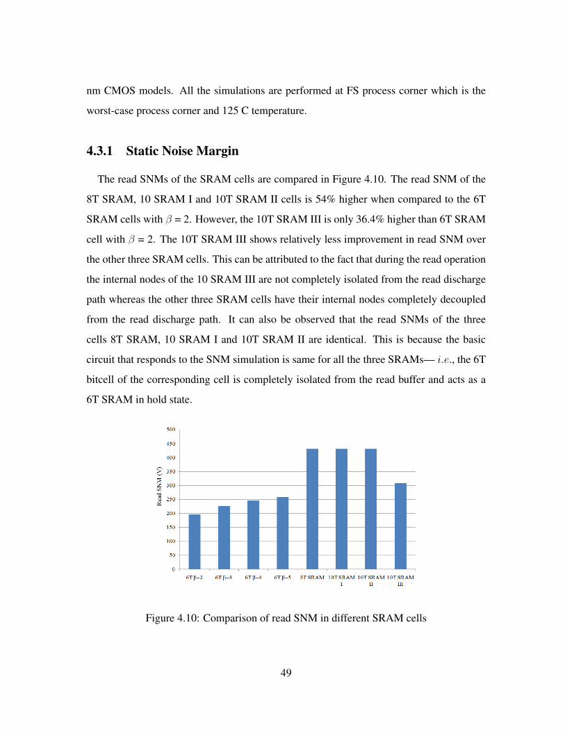
The read SNMs of the SRAM cells are compared in Figure 4.10. The read SNM of the
8T SRAM, 10 SRAM I and 10T SRAM II cells is 54% higher when compared to the 6T
SRAM cells with β = 2. However, the 10T SRAM III is only 36.4% higher than 6T SRAM
cell with β = 2. The 10T SRAM III shows relatively less improvement in read SNM over
the other three SRAM cells. This can be attributed to the fact that during the read operation
the internal nodes of the 10 SRAM III are not completely isolated from the read discharge
path whereas the other three SRAM cells have their internal nodes completely decoupled
from the read discharge path. It can also be observed that the read SNMs of the three
cells 8T SRAM, 10 SRAM I and 10T SRAM II are identical. This is because the basic
circuit that responds to the SNM simulation is same for all the three SRAMs— i.e., the 6T
bitcell of the corresponding cell is completely isolated from the read buffer and acts as a
6T SRAM in hold state.
Figure 4.10: Comparison of read SNM in different SRAM cells
49

4.3.2 Write Noise Margin
The WSNM comparison between the SRAM cells is illustrated in Figure 4.11. The
proposed SRAM cells typically employ a write-assist technique to boost the writability
of the cell and improve the WSNM. Before the onset of the write operation of the 10T
SRAM cell I, the VVdd floats instead of supplying Vdd . This decrease in the supply
voltage effectively weakens the SRAM cell making it easy for the access transistors to
overpower the node voltages, which in turn improves the WSNM. For the 10T SRAM II,
in the write mode both the wordlines WL and WWL are enabled to transfer the write data
to the cell nodes from the bitlines. Since this SRAM has two series access transistors
in order to perform the write operation, writability is a critical issue. The writability in
this implementation is improved by boosting the voltages of WL and WWL by 100 mV
during the write operation, which improves the writability by making the access transistors
stronger than the SRAM cell. The 10T SRAM III cell has the best write noise margin
among all the SRAM cells compared in this paper (Figure 4.11). Compared to the 6T cell,
the effective strength of the pull-down transistor is reduced in the 10TSRAM III cell during
the ‘1’ to ‘0’ input transition, which boosts the WSNM of the cell.
50

Figure 4.11: Comparison of write SNM in different SRAM cells
4.3.3 Impact of Process Variations
The read stability of the SRAM cells in the presence of variations in Vth and gate length
Leff is evaluated. The Vth variation due to random dopant fluctuations is the major source
of variability in modern nanoscale SRAMs [20]. Therefore, it is of utmost importance to
evaluate any memory design in the presence of Vth variations so as to ensure that the design
meets the yield requirements. In order to simulate the RDF induced intra-die (mismatch
between the adjacent transistors on the same die) variation, each of the Vth of the transistors
in a cell is assumed to be an independent random parameter with a Gaussian distribution.
In addition, each parameter is assumed to have three sigma (3σ) variations of 10% [32]
[33]. Monte Carlo (MC) simulations for 1000 samples were performed on the SRAM cells
and the corresponding read SNM is calculated for each MC run. Similarly, the SRAM cells
are evaluated for Leff variation. Since all the simulations are performed at Vdd = 1.2 V, as
a guideline ‘µ−6σ’ of the SNM is required to exceed 48 mV (4% of the supply voltage) to
achieve 90% yield for 1Mbit SRAMs. Therefore, it is obvious that a high mean read SNM
51

and a low standard deviation are ideal to meet the yield criterion.
The read SNM distribution of the 8T SRAM cells as obtained from the MC simulations
is illustrated in Figure 4.12. Table 4.3 shows the read SNM comparison of all the SRAM
cells when subjected to Vth variation. The mean read SNM of the 8T SRAM cell is above
390 mV, 60% higher than that of the 6T SRAM cell. The standard deviation of the 8T
SRAM is 10.55% less than the 6T SRAM cell. The 8T SRAM cell passes the yield test
by a considerable margin whereas the 6T SRAM cell does not. The 8T SRAM cell when
subjected to Leff variations shows better robustness when compared to the 6T SRAM cell,
as shown in Table 4.4 and Figure 4.13. The mean read SNM of the 8T SRAM cell is 60%
higher than that of the 6T SRAM cell and the standard deviation of the 8T SRAM is 12.55%
less than the 6T SRAM cells. The cell yield criterion is met by the 8T cell.
0.25 0.3 0.35 0.4 0.45 0.50
10
20
30
40
50
60
70
80
90
100
Read Static Noise Margin (V)
Occurences
8T SRAMMean=397.1mVSD=56.55mV
Figure 4.12: Read SNM distribution of the 8T SRAM cells as obtained from the MC sim-
ulations in presence of Vth variations
52

0.25 0.3 0.35 0.4 0.45 0.50
10
20
30
40
50
60
70
80
90
100
Read Static Noise Margin (V)
Occurences
8T SRAMMean=392.6mVSD=54.79mV
Figure 4.13: Read SNM distribution of the 8T SRAM cells as obtained from the MC sim-
ulations in presence of Leff variations
The 10T SRAM I and the 10 SRAM II cells outperform the 6T cell in the case of Leff
variation too (Figure 4.14 and Table 4.4). The mean read SNM of both the cells is higher
than the 6T cell by 60.08% and the standard deviation is lesser by 13.23% as shown in the
Table 4.4. The major advantage of the 10T SRAM I and II cells is the yield criterion, which
is met by both the cells with a considerable margin whereas the 6T cell fails to meet the
yield criterion. The 10T SRAM I and 10T SRAM II cells are subjected to Vth variations
(Figure 4.15 and Table 4.3). There is a substantial improvement in the mean read SNM as
well as the standard deviation of the 10T I cell when compared to the 6T cell. The mean
read SNM of the 10T I cell is 58.3% higher than the traditional 6T cell. The standard
deviation is 15.74% lower in the 10T I cell. Similarly, the read SNM of the 10T II cell
is 58.3% higher than the conventional 6T cell and the standard deviation is 15.74% lower
than the 6T cell.
53

Table 4.3: Impact of random intra-die Vth variations on the read SNM of SRAM cells
Mean of SNM SD of SNM Yield Criterion
SRAM µ (mV) σ (mV) µ− 6σ (mV) (µ− 6σ)>48 mV
6T SRAM 164.9 63.25 0 Fail
8T SRAM 397.1 56.55 57.8 Pass
10T SRAM I 396.3 53.29 76.56 Pass
10T SRAM II 396.3 53.29 76.56 Pass
10T SRAM III 274.49 44.14 9.65 Fail
0.25 0.3 0.35 0.4 0.45 0.50
10
20
30
40
50
60
70
80
90
100
Read Static Noise Margin (V)
Occurences
10T SRAM IMean=393.7mVSD=55.92mV
Figure 4.14: Read SNM distribution of the 10T I SRAM cells as obtained from the MC
simulations in presence of Leff variations
54

0.25 0.3 0.35 0.4 0.45 0.50
10
20
30
40
50
60
70
80
90
Read Static Noise Margin (V)
Occurences
10T SRAM IMean=396.3mVSD=53.29mV
Figure 4.15: Read SNM distribution of the 10T I SRAM cells as obtained from the MC
simulations in presence of Vth variations
The 10 SRAM III cell is also evaluated in the presence of Vth and Leff variations and the
MC simulations for the read SNM are illustrated in Figures 4.16 and 4.17. The 10T SRAM
III exhibits higher read SNM of 39.92% in the presence of Vth variation and 43.25% in the
presence of Leff variation when compared to the 6T SRAM cell as shown in Tables 4.3 and
4.4. However, the 10T SRAM fails to satisfy the yield criterion by a narrow margin in both
the cases. At this juncture, it is important to notice two primary differences between 10T III
cell and other bitcells. During the read operation, the 8T, 10T I and 10T II cells completely
isolate the internal nodes of the bitcell from the read path. Therefore, even though one
of the bitlines is discharged, the internal nodes are decoupled from the discharge path.
The 10T III bitcell works on a different principle altogether. During the read operation,
the NFR/NFL forms a positive feedback with the inverter PR-NR1-NR2/PL-NL1-NL2.
This feedback helps to raise the threshold voltage at VR(VL) when BL(BR) discharges via
VL(VR), thereby avoiding read failure. However, in the presence of process variations,
mismatch is introduced between NFR/NFL and NR1-NR2/NL1-NL2, which weakens the
55

Table 4.4: Impact of random intra-die Leff variations on the read SNM of SRAM cells
Mean of SNM SD of SNM Yield Criterion
SRAM µ (mV) σ (mV) µ− 6σ (mV) (µ− 6σ)>48 mV
6T SRAM 157 64.45 0 Fail
8T SRAM 392.6 54 68.6 Pass
10T SRAM I 393.37 55.92 57.85 Pass
10T SRAM II 393.37 55.92 57.85 Pass
10T SRAM III 276.7 43.9 13.3 Fail
Schmitt trigger, thereby making the cell vulnerable to read failure. Hence, the 10T III cell
is more vulnerable to read failure when compared to the 8T, 10T I and 10T II SRAM cells.
56

0.1 0.2 0.3 0.40
10
20
30
40
50
60
70
80
90
100
Read Static Noise Margin (V)
Occurences
10T SRAM IIIMean=276.6mVSD=43.9mV
Figure 4.16: Read SNM distribution of the 10T III SRAM cells as obtained from the MC
simulations in presence of Leff variations
0.1 0.2 0.3 0.40
10
20
30
40
50
60
70
80
90
Read Static Noise Margin (V)
Occurences
10T SRAM IIIMean=274.49mVSD=44.14mV
Figure 4.17: Read SNM distribution of the 10T III SRAM cells as obtained from the MC
simulations in presence of Vth variations
57

4.4 Proposed 9T SRAM
4.4.1 Static Noise Margin
The butterfly curves representing the VTCs of the two inverters of the proposed 9T bitcell
during the read and retention states are shown in Figure 4.18. In the standard 6T SRAM
cell, during the read operation, the node containing ‘0’ experiences a rise in voltage which
makes the cell vulnerable to read failure. Previously published 8T, 10T and 9T SRAM cells
isolate the read path from the internal nodes of the bitcell to improve the read SNM. The 9T
SRAM cell also employs a read buffer which isolates the bitline from the internal nodes of
the bitcell. This increases the static noise margin of the 9T SRAM cell as shown in Figure
4.18. The read SNMs of the standard 6T SRAM cell at β = 2, 3, 4, in addition to 8T, 10T,
9T and the proposed 9T SRAM cells are illustrated in Figure 4.19. The read static noise
margin of the proposed 9T SRAM cell is 2.5 times greater than the 6T SRAM cell with β
= 2 and 2 times greater than 6T SRAM with β = 3. Therefore, even though the cell-ratio of
the 6T SRAM cell is increased, it exhibits lesser read stability whe compared to proposed
9T SRAM cell.
58

0 0.2 0.4 0.6 0.8 1 1.2 1.40
0.2
0.4
0.6
0.8
1
1.2
1.4
Vin
(V)
Vout (
V)
Read SNM
Hold SNM
SNM431mV
Figure 4.18: The read and hold static noise margins of the proposed 9T SRAM circuit. The
cell exhibits higher SNM for both states compared to the standard 6T SRAM cell.
Figure 4.19: Comparison of Read Static Noise Margins of different SRAM cells with the
proposed 9T SRAM cell.
59

4.4.2 Bitline Leakage
The proposed 9T SRAM cell prevents the bitline leakage independent of the node voltage
driving the read buffer. This is an important improvement over the previously published
designs which attempt to address the bitline leakage but achieve it partially: only when
the node voltage driving the read buffer is ‘0’. The Figure 4.20 compares the SRAM
cells based on the node voltage driving the read buffer since this voltage can bring about a
significant change in the amount of bitline leakage. The voltage of one of the internal nodes
of the cell connected to the read buffer will be referred as the “drive voltage” for the rest
of the paper. For example, the drive voltage for the proposed 9T SRAM cell would be the
voltage at node Qb. The proposed 9T SRAM cell in this paper successfully maintains the
node voltage N at VDD during the standby state(see Figure 3.6). This prevents any bitline
leakage independent of the drive voltage. Leakage would exist only through transistors E3
and E4 from the node N, which is reduced due to the transistor stack E3 and E4 as shown
in the Fig 3.6. It can be observed from the Figure 4.20 that among all the cases except
the proposed 9T SRAM cell, the leakage savings are more when the drive voltage is ‘0’.
The reason is that when the drive voltage is ‘0’, it creates a stack effect in all the 8T, 9T
and 10T cells, whereas the other case (drive voltage = ‘1’) fails to create any effect, as
illustrated in the graph. In contrast, the proposed 9T SRAM cell achieves bitline leakage
power savings independent of its drive voltage Qb. The bitline leakage power consumption
of the proposed 9T SRAM cell is reduced by up to 79%, 76% and 39% when compared to
the previously published 8T, 10T and 9T SRAM cells, respectively.
60

Figure 4.20: Comparison of bitline leakage of different SRAM cells with the proposed 9T
SRAM cell.
4.4.3 Impact of Process Variations
In this section, the read stability of the SRAM cells due to process fluctuations in the
channel length and the threshold voltage of the transistors is evaluated. The channel length
and the threshold voltage are assumed to have a normal Gaussian statistical distributions.
Each parameter is assumed to have a three sigma (3σ) variation of 10% [32]. Monte Carlo
simulations with 5000 occurrences are performed to evaluate the impact of process vari-
ations on the read stability of the 6T SRAM and 9T SRAM cells. The statistical SNM
distributions of the 6T and the proposed SRAM cells are shown in Figure 4.21. The mean
read static noise margin of the 9T cells is approximately 2.4 times when compared to the
6T SRAM cell with β = 2. This increase in static noise margin can be attributed to the fact
that the 9T SRAM cell achieves a complete isolation of the internal nodes from the read
discharge path. The standard deviation of the 9T cells is 14.6% less than the 6T cells which
implies a lesser spread in the SNM distribution in the proposed 9T SRAM cells.
61

0 0.1 0.2 0.3 0.4 0.50
50
100
150
200
250
Read Static Noise Margin (V)
Occurrences
Proposed9T SRAM
Mean=396mVSD=54.1mV
6T SRAMMean=165mVSD=63.4mV
Figure 4.21: Statistical SNM distributions of the proposed 9T SRAM cell in comparison
with the 6T SRAM cell.
The impact of process variations on the yield of the proposed 9T SRAM cell in the
presence of process variations can be assessed by evaluating the yield criterion from the
monte carlo simulations. The proposed 9T SRAM has a higher mean read SNM and a lower
standard variation when compared to the 6T SRAM cell. The yield criterion is evaluated
as shown in the Table 4.5. The proposed 9T SRAM cell satisfies the 90% yield criterion.
4.4.4 Area Overhead
The bitcell area is an important parameter for cache design since it directly relates to
the cache footprint, array density and the overall SoC cost. The previous-published SRAM
bitcells have a substantial area overhead when compared to the traditional 6T SRAM cell.
Table 4.6 illustrates the area overhead in terms of the number of MOSETS, wordlines and
bitlines required for each SRAM cell. It can be observed that in spite of the 8T (33% area
62

Table 4.5: Impact of process variations on the proposed 9T SRAM cells
Mean of SNM SD of SNM Yield Criterion
SRAM µ (mV) σ (mV) µ− 6σ (mV) (µ− 6σ)>48 mV
6TSRAM 165.8 63.43 0 Fail
Proposed 9T SRAM 396.3 54.13 71.52 Pass
Table 4.6: Area overhead comparison of different SRAM cells [24] [25] [26] [27] [34]
6T 8T 9T 10T 10T New 9T
SRAM SRAM SRAM SRAM SRAM I SRAM II, III SRAM
No. of MOSFETs 6 8 9 10 10 9
No. of WL 1 2 2 2 2 2
No. of BL 2 3 3 3 2 2
overhead) and 10T cells (66% area overhead) they offer better read and write stability com-
pared to the conventional 6T cell. The proposed 9T cell exhibits better area savings when
compared to 8T[24], 9T[34], 10T I[25], 10T II[26] and 10T III[27] cells. The proposed 9T
cell has one less bitline when compared to 8T, 9T and 10T I SRAM cells. The proposed
design also has one less transistor compared to the 10T I, II, and III cells. Even though the
proposed 9T SRAM has significant area overhead compared to the conventional 6T SRAM
cell, it outperforms the 6T SRAM cell when the read static noise margin and bitline leakage
values are compared. The 8T SRAM cell has one less transistor than the proposed 9T cell
but it is also important to notice that the 8T SRAM cell has an extra bitline and consumes
more bitline leakage power.
63

5. Conclusions
The stability of the Static Random Access Memories in the presence of process vari-
ations is a growing concern for circuit designers in the present nanoscale regime. This
research investigates the traditional 6T SRAM cell from a stability perspective. The im-
pact of process variations on the traditional 6T SRAM is evaluated and their impact on
6T SRAM yield is established. The present work proves that, in the presence of process
variations, the 6T SRAM cell fails to satisfy the “µ − 6σ” yield criterion. This reduced
yield due to the results in increased design and fabrication costs and eventually increases
the time-to-market of the chips. Therefore, it is imperative that the SRAM is designed to
be robust in the presence of process variations.
In order to address this issue, various SRAM bitcell topologies were published earlier.
These cells also employ read or write assist or a combination of both these techniques
in order to boost the read/write performance of the SRAM cell. In the present work, the
8T [24], 9T [34], 10T I [25], 10T II [26], 10T III [27] SRAM circuits are designed and
evaluated for correct functionality. Furthermore, the robustness of these cells to process
variations are evaluated by performing Monte Carlo simulations and evaluating the yield
criterion. All these cells are succesful in addressing the read stability problem associated
with the 6T SRAM cell. However, the cells suffer from bitline leakage problem which
results in a wrong value being read by the sense-amplifier and also places constraints on
the number of cells that can be accomodated on the bitlines.
In order to address the issue of bitline leakage, a new 9T SRAM cell is proposed in
this work. The proposed 9T cell simultaneously addresses the read stability as well as the
bitline leakage problems. The 9T cell is designed and verified for succesful read and write
64

operations. The butterfly curves for the proposed cell are plotted and the read/hold SNMs
are evaluated and it is proved that the read SNM of the proposed design is better than that of
the 6T SRAM cell. The impact of process variations on the stability of the proposed design
is evaluated by performing 5000 MC simulations. The proposed design satisfies “µ− 6σ”
yield criterion. The bitline leakage power consumption by the current design is evaluated
and compared with the previous designs. The present research provides a design framework
to perform simulations to calculate the SNM of different SRAM cells. The present work
also provides a framework to perform Monte Carlo simulations in the presence of process
variations.
65

6. Future Work
The proposed 9T SRAM cell can be further improved. Some suggestions for future work
are:
1. Read and write-assist techniques can be explored which could give a better read and
write performance for the proposed design. During the read operation, the RWL
voltage which drives the transistors on the read discharge path can be boosted to
improve the read performance.
2. Techniques to boost the write performance can be implemented. The writability of
the SRAM cell can be improved by decreasing the pull-up ratio of the cell. The
write performance can also be boosted by decreasing the supply voltage to the bitcell
during the write operation.
3. The rapid growth of battery operated handheld devices like cell phones, GPS devices,
music players etc have increased research in decreasing the power consumption of
these devices. These devices typically use low power SoCs. Since the caches make
up the bulk of the transistors on SoCs, it is imperative that the cache design incor-
porates techniques to reduce the power consumption. The proposed SRAM can be
investigated for sub-threshold operation using the sub-threshold library created in the
Hardware Design Lab.
4. The Monte Carlo simulations typically consume a large amount of time depending on
the number of monte carlo runs or the number of random variables. The Monte Carlo
simulations can be performed in parallel by leveraging the Computer Engineering
cluster in order to reduce simulation time.
66

References
[1] B. H. Calhoun, Y. L. Cao, X. Mai, K. L. T. Oileggi, R. A. Rutenbar, and K. L. Shepard,
“Digital circuit design challenges and opportunities in the era of nanoscale cmos,”
Proceedings of the IEEE, vol. 96, no. 2, pp. 343–365, 2007.
[2] H. Raymond and P. Wang, “Variability in sub-100nm sram designs,” in IEEE Inter-
national Conference on Computer Aided Design, pp. 347–352, San Jose, California,
USA, 2004.
[3] M. Orshansky, S. Nassif, and D. Boning, Design for Manufacturability and Statistical
Design, Springer Publications, Springer US, 233 Spring Street, New York 10013,
2007.
[4] C. C. Chiang and J. Kawa, Design for Manufacturability and Yield for Nano-Scale
CMOS, Springer Publications, P.O.Box 17, 3300 AA Dordrecht, The Netherlands,
2007.
[5] V. Mehrotra, Modeling the effects of systematic process variation on circuit perfor-
mance, PhD thesis, Massachusetts Institute of Technology, 2001.
[6] A. J. Bhavnagarwala, T. Xinghai, and J. D. Meindl, “The impact of intrinsic device
fluctuations on cmos sram cell stability,” IEEE Journal of Solid-State Circuits, vol. 36,
no. 4, pp. 658–665, 2001.
[7] S. Nassif, “Delay variability: sources, impacts and trends,” in IEEE International
Solid-State Circuits Conference, pp. 368–369, San Francisco, California, USA, 2000.
[8] C. A. Andrew, R. Brown, Gareth Roy and C. Riddet, “Simu-
lation of intrinsic parameter fluctuations in nano-cmos devices”
www.elec.gla.ac.uk/groups/dev_mod/research/atomistic.php.
[9] J. A. Croon, G. Storms, S. Winkelmeier, I. Pollentier, M. Ercken, S. Decoutere,
W. Sansen, and H. E. Maes, “Line edge roughness: characterization, modeling and
67

impact on device behavior,” in International Electron Devices Meeting, pp. 307–310,
San Francisco, California, USA, 2002.
[10] K. A. Bowman, T. Xinghai, J. C. Eble, and J. D. Meindl, “Impact of extrinsic and
intrinsic parameter fluctuations on cmos circuit performance,” IEEE Journal of Solid-
State Circuits, vol. 35, no. 8, pp. 1186–1193, 2000.
[11] H. Mahmoodi, S. Mukhopadhyay, and K. Roy, “Estimation of delay variations due to
random-dopant fluctuations in nanoscale cmos circuits,” IEEE Journal of Solid-State
Circuits, vol. 40, no. 9, pp. 1787–1796, 2005.
[12] S. Borkar, “Designing reliable systems from unreliable components: the challenges of
transistor variability and degradations,” IEEE Micro, vol. 25, no. 6, pp. 10–16, 2005.
[13] K. Takeuchi, T. Fukai, T. Tsunomura, A. T. Putra, A. Nishida, S. Kamohara, and T. Hi-
ramoto, “Understanding random threshold voltage fluctuation by comparing multiple
fabs and technologies,” in IEEE International Electron Devices Meeting, pp. 467–
470, Washington, D.C, USA, 2007.
[14] P. A. Stolk, F. P. Widdershoven, and D. B. M. Klaassen, “Modeling statistical dopant
fluctuations in mos transistors,” IEEE Transactions on Electron Devices, vol. 45,
no. 9, pp. 1960–1971, 1998.
[15] D. A. Hodges, H. G. Jackson, and R. A. Salve, Analysis and Design of Digital Inte-
grated Circuits, Mc-Graw Hill, 1221 Avenue of the Mericas, New York, NY 10020,
2003.
[16] J. M. Rabaey, A. P. Chandrakasan, and B. Nikolic, Digital Integrated Circuits, Pren-
tice Hall Electronics and VLSI Series, Pearson Education Inc., Upper Saddle River,
New Jersey 07458, 2003.
[17] M. Graef, R. Mahnkopf, H. Ishiuchi, T. Osada, J. T. Moon, J. Roh,
C. H. Diaz, B. Lin, P. Apte, B. Doering, P. Gargini, W. Arden, and
P. Cogez, “International technology roadmap for semiconductors-2008 update,”
http://www.itrs.net/Links/2008ITRS/Home2008.htm.
[18] http://en.wikipedia.org/wiki/Montecito_(processor).
68

[19] A. Pavlov and M. Sachdev, CMOS SRAM Circuit Design and Parametric Test in
Nano-Scaled Technologies, Springer Publications, Springer US, 233 Spring Street,
New York 10013, 2008.
[20] S. Mukhopadhyay, H. Mahmoodi, and K. Roy, “Modeling of failure probability and
statistical design of sram array for yield enhancement in nanoscaled cmos,” IEEE
Transactions on Computer-Aided Design of Integrated Circuits and Systems, vol. 24,
no. 12, pp. 1859–1880, 2005.
[21] E. Seevinck, F. J. List, and J. Lohstroh, “Static-noise margin analysis of mos sram
cells,” IEEE Journal of Solid-State Circuits, vol. 22, no. 5, pp. 748–754, 1987.
[22] K. Zhang, Embedded Memories for Nano-scale VLSIs, Springer Publications,
Springer US, 233 Spring Street, New York 10013, 2009.
[23] S. A. Tawfik and V. Kursun, “Low power and robust 7t dual-vt sram circuit,” in IEEE
International Symposium on Circuits and Systems, pp. 1452–1455, Seattle, Washing-
ton, D.C, USA, 2008.
[24] L. Chang, D. M. Fried, J. Hergenrother, J. W. Sleight, R. H. Dennard, R. K. Montoye,
L. Sekaric, S. J. McNab, A. W. Topol, C. D. Adams, K. W. Guarini, and W. Haensch,
“Stable sram cell design for the 32 nm node and beyond,” in Symposium on VLSI
Technology, pp. 128–129, Kyoto, Japan, 2005.
[25] B. H. Calhoun and A. P. Chandrakasan, “A 256-kb 65-nm sub-threshold sram design
for ultra-low-voltage operation,” IEEE Journal of Solid-State Circuits, vol. 42, no. 3,
pp. 680–688, 2007.
[26] I. J. Chang, J. J. Kim, S. P. Park, and K. Roy, “A 32 kb 10t sub-threshold sram array
with bit-interleaving and differential read scheme in 90 nm cmos,” IEEE Journal of
Solid-State Circuits, vol. 44, no. 2, pp. 650–658, 2009.
[27] P. K. Jaydeep, K. Keejong, and K. Roy, “A 160 mv, fully differential, robust schmitt
trigger based sub-threshold sram,” in International Symposium on Low Power Elec-
tronics, pp. 171–176, Portland, Oregon, USA, 2007.
[28] A. J. Bhavnagarwala, S. Kosonocky, C. Radens, K. Stawiasz, R. Mann, Y. Qiuyi, and
C. Ken, “Fluctuation limits and scaling opportunities for cmos sram cells,” in IEEE In-
ternational Electronic Devices Meeting, pp. 659–662, Washington, D.C, USA, 2005.
69

[29] J. Wang, N. Satyanand and B. H. Calhoun, “Analyzing static and dynamic write mar-
gin for nanometer srams,” in International Symposium on Low Power Electronics and
Design, pp. 64–67, Newport, California, USA, 2004.
[30] B. Cheng, S. Roy, and A. Asenov, “The scalability of 8t-sram cells under the influ-
ence of intrinsic parameter fluctuations,” in European Solid State Device Research
Conference, pp. 93–96, Sevilla, Spain, 2007.
[31] P. A. Stolk, H. P. Tuinhout, R. Duffy, E. Augendre, L. P. Bellefroid, M. J. B. Bolt,
J. Croon, C. J. J. Dachs, F. R. Huisman, A. J. Moonen, Y. V. Ponomarev, R. F. M.
Roes, R. M. Da, E. Seevinck, K. N. Sreerambhatla, R. Surdeanu, R. M. D. A. Velghe,
M. Vertregt, M. N. Webster, W. N. K. J. Van, and D. A. T. A. Zegers-Van, “Cmos
device optimization for mixed-signal technologies,” in International Electron Devices
Meeting, pp. 10.2.1–10.2.4, Washington, D.C, USA 2001.
[32] L. Zhiyu and V. Kursun, “High read stability and low leakage cache memory cell,”
in IEEE International Symposium on Circuits and Systems, pp. 2774–2777, New Or-
leans, Louisiana, USA, 2007.
[33] S. Ashish, B. Robert, B. David, and S. Dennis, “Modeling and analysis of leak-
age power within-die process variations,” in International Symposium on Low Power
Electronics and Design, pp. 64–67, Monterey, California, USA, 2002.
[34] S. Lin, Y. B. Kim, and F. Lombardi, “A highly-stable nanometer memory for low-
power design,” in 2008 IEEE International Workshop on Design and Test of Nano
Devices, Circuits and Systems, pp. 17–20, Cambridge, Massachusetts, USA, 2008.
70

A. Spice Netlist
Spice netlist used to determine butterfly curves for the 6T SRAM cell.
*Operating Conditions and Setup
*Vdd: 1.2V
*FET: Normal
*Technology: IBM CMOS 65nm
*Temperature: 125C
*Mismatch: Off
*Process Corner: FS
*Misc: None
*Cell-Ratio: 2
*Pull-up Ratio: 1
*Include the technology file and define operating conditions
Technology file and operating conditions are not shown due to copyright policies.
.option tnom = 125
.param supply = 1.2
*Mosfets
xl1 innode outnode vdd vdd pfet W=65n L=65n
xd1 innode outnode gnd gnd nfet W=130n L=65n
xl2 outnode innode vdd vdd pfet W=65n L=65n
xd2 outnode innode gnd gnd nfet W=130n L=65n
xa1 vdd vdd innode gnd nfet W=65n L=65n
xa2 vdd vdd outnode gnd nfet W=65n L=65n
*power supply
VVDD VDD 0 supply
Vin outnode 0 0 pulse(0,supply, 0.1n,0.1n,0.1n, 10n,20n)
71

*dc sweep analysis
.DC Vin 0 supply 0.001
*Output Format
.options post
.print dc V(innode)
.END
72