a programmable uwb-ir wireless sensor node prototype
TRANSCRIPT

Kungliga Tekniska hogskolan (KTH)Skolan for informations- och kommunikationsteknik (ICT)
A Programmable UWB-IR Wireless
Sensor Node Prototype, Using the Intel
WISP Platform
by
Ramon Boixadera Planas
Examiner: Prof. Li-Rong Zheng
Stockholm, November 2010


“
If knowledge can create problems, it is not
through ignorance that we can solve them.
”
Isaac Asimov (1920-1992)

Kungliga Tekniska hogskolan (KTH)
Abstract
Skolan for informations- och kommunikationsteknik (ICT)
Department of Electronic Systems
by Ramon Boixadera Planas
Remote sensing and measuring is becoming more important with accelerating advances in tech-
nology. The ability to process large amounts of data using the internet and advanced digital
signal processing techniques means that data can be collected, processed, organized, and in-
terpreted as never before in history. This opens up possibilities of detailed monitoring of the
environment, wildlife habitats, complex industrial machinery, aerospace vehicle platforms, and
consumer equipment and the home environment. Sensing has advanced from manual meter read-
ing to centralized data acquisition systems to a new era of distributed wireless sensor networks.
The aim of this work is to design a programmable prototype for a UWB RFID node. UWB
RFID technology develops asymmetric wireless links so as to achieve high throughput, long
operating range, high security, low power consumption and low manufacturing cost. This node
can be compatible with EPC Global C1 G2 or develop the UWB RFID protocol, and includes a
7-segment display, thermometer and accelerometer. It is built in conjunction with Intel WISP4.1
DL. There is a complete explanation of the hardware and the software designed as well as an
analysis of a wide range of performance measurements.
Moreover, in this work, an innovative node prototype is proposed. This node presents, among
other features, a power scavenging unit which may be more than twice as powerful than Intel
WISP4.1 DL. This improvement is caused by two aspects. Firstly, it includes a positive an a
negative branch to develop a multi-stage bridge rectifier, dislike the single one in Intel WISP;
one is supplying the node while the other one is charging. Secondly, it permits to adjust the
number of stages in each branch so as to maximise the power obtained.


Acknowledgements
I would like to start thanking Kungliga Tekniska Hogskolan. Leaving Spain for studies
was a hard decision to me, but “you” made it easy and pleasant. I am really grateful
for giving me the opportunity and the facilities to carry out my Master’s Thesis here in
Sweden and for discovering me this amazing country.
I also want to thank my supervisor David Sarmiento all the support, advices and time
he dedicated to me. I am sure that this work would not be the same without all the
effort you devoted. Thank you for the whole humanity you demonstrate each and every
day.
Jose and Tuton, thank you for all the “motivating” cigarettes we shared, the knowledge
we exchanged and the time we spent together at KTH. Thank also to all the friends I
met here (Alvaro, Ricky, Javier, Clement, Willeke, Rosa, Vero, Brice, Christian, Mario,
Fabiano, ...) who helped me to enjoy this experience.
To the other side of the continent, Catalunya, I would like to mention the people who
drove me to go on my studies for several years: Jordi, Vıctor, Marc, Lluıs, Miquel, Jesus,
Gerard, Aleix, Dani, Yasmina, ... No se ni a que em dedicaria ara mateix si no fos per
vosaltres. Merci a tots!
Last but not least, I need to give special thanks to my big family. Mil gracies per tot
l’amor, per la paciencia que heu tingut, per la llibertat que m’heu donat i per ser on sou
i com sou. Tots i cadascun de vosaltres m’ha ajudat a ser qui soc. Moltıssimes gracies
Ramon, Angelina, Jordi, Mary, Eva, Ester i Clara.
vii


This page is intentionally left blank


Contents
Abstract v
List of Figures xv
List of Tables xix
Abbreviations xxi
1 Introduction 1
1.1 RFID . . . . . . . . . . . . . . . . . . . . . . . . . . . . . . . . . . . . . . 2
1.2 UWB . . . . . . . . . . . . . . . . . . . . . . . . . . . . . . . . . . . . . . 4
1.3 UWB RFID system . . . . . . . . . . . . . . . . . . . . . . . . . . . . . . 6
1.4 Existing nodes . . . . . . . . . . . . . . . . . . . . . . . . . . . . . . . . . 7
1.4.1 Intel’s WISP4.1 DL . . . . . . . . . . . . . . . . . . . . . . . . . . 7
1.4.2 Berkeley’s Mote . . . . . . . . . . . . . . . . . . . . . . . . . . . . . 7
1.5 Motivation . . . . . . . . . . . . . . . . . . . . . . . . . . . . . . . . . . . 8
1.6 Thesis overview . . . . . . . . . . . . . . . . . . . . . . . . . . . . . . . . . 9
2 Intel WISP4.1 DL 11
2.1 Hardware . . . . . . . . . . . . . . . . . . . . . . . . . . . . . . . . . . . . 11
2.2 Software . . . . . . . . . . . . . . . . . . . . . . . . . . . . . . . . . . . . . 13
3 System implementation 17
3.1 Functional description . . . . . . . . . . . . . . . . . . . . . . . . . . . . . 18
3.2 Hardware . . . . . . . . . . . . . . . . . . . . . . . . . . . . . . . . . . . . 18
3.2.1 Block diagram . . . . . . . . . . . . . . . . . . . . . . . . . . . . . 18
3.2.2 Physical connection . . . . . . . . . . . . . . . . . . . . . . . . . . 21
3.3 Software . . . . . . . . . . . . . . . . . . . . . . . . . . . . . . . . . . . . . 22
3.3.1 Adaptation to the Reader . . . . . . . . . . . . . . . . . . . . . . . 23
3.3.1.1 Reader inspection . . . . . . . . . . . . . . . . . . . . . . 23
3.3.1.2 Clock modification . . . . . . . . . . . . . . . . . . . . . . 26
3.3.2 Operating modes . . . . . . . . . . . . . . . . . . . . . . . . . . . . 28
3.3.2.1 OpMode 1 . . . . . . . . . . . . . . . . . . . . . . . . . . 29
3.3.2.2 OpMode 2 . . . . . . . . . . . . . . . . . . . . . . . . . . 31
3.3.2.3 OpMode 3 . . . . . . . . . . . . . . . . . . . . . . . . . . 33
xi

xii CONTENTS
4 Measurements 41
4.1 Transmission line to uplink antenna. Reflection coefficient (S11) . . . . . . 41
4.2 UWB transmission. Pulse shape . . . . . . . . . . . . . . . . . . . . . . . 43
4.3 Current consumption . . . . . . . . . . . . . . . . . . . . . . . . . . . . . . 44
4.3.1 UWB transmitter . . . . . . . . . . . . . . . . . . . . . . . . . . . . 44
4.3.2 7-segment display . . . . . . . . . . . . . . . . . . . . . . . . . . . . 46
4.3.3 Extension PCB . . . . . . . . . . . . . . . . . . . . . . . . . . . . . 48
4.4 Communication range . . . . . . . . . . . . . . . . . . . . . . . . . . . . . 51
4.5 Performance tests . . . . . . . . . . . . . . . . . . . . . . . . . . . . . . . . 52
4.5.1 “Ordinary” tag . . . . . . . . . . . . . . . . . . . . . . . . . . . . . 53
4.5.2 “Battery-equipped” tag . . . . . . . . . . . . . . . . . . . . . . . . 53
4.5.3 “No-display” tag . . . . . . . . . . . . . . . . . . . . . . . . . . . . 54
4.5.4 “Battery-equipped no-display” tag . . . . . . . . . . . . . . . . . . 54
4.5.5 Extra capacitor . . . . . . . . . . . . . . . . . . . . . . . . . . . . . 55
4.6 Harvester’s charging time . . . . . . . . . . . . . . . . . . . . . . . . . . . 57
4.7 System specifications . . . . . . . . . . . . . . . . . . . . . . . . . . . . . . 58
5 Conclusions 61
5.1 Future work . . . . . . . . . . . . . . . . . . . . . . . . . . . . . . . . . . . 62
A Intel WISP4.1 DL. Schematic and layout images 65
A.1 Schematic . . . . . . . . . . . . . . . . . . . . . . . . . . . . . . . . . . . . 65
A.2 Layout images . . . . . . . . . . . . . . . . . . . . . . . . . . . . . . . . . 65
B Extension PCB. Schematic, layout images and images 69
B.1 Schematic . . . . . . . . . . . . . . . . . . . . . . . . . . . . . . . . . . . . 69
B.2 Layout images . . . . . . . . . . . . . . . . . . . . . . . . . . . . . . . . . 69
B.3 Images . . . . . . . . . . . . . . . . . . . . . . . . . . . . . . . . . . . . . . 70
C Measurements 77
C.1 Transmission line to uplink antenna. Reflection coefficient (S11) . . . . . . 77
C.2 UWB transmission. Pulse shape . . . . . . . . . . . . . . . . . . . . . . . 78
C.3 Current consumption . . . . . . . . . . . . . . . . . . . . . . . . . . . . . . 79
C.3.1 UWB transmitter . . . . . . . . . . . . . . . . . . . . . . . . . . . . 79
C.3.2 7-segment display . . . . . . . . . . . . . . . . . . . . . . . . . . . . 80
C.3.3 Extension PCB . . . . . . . . . . . . . . . . . . . . . . . . . . . . . 81
C.4 Communication range . . . . . . . . . . . . . . . . . . . . . . . . . . . . . 84
C.5 Performance tests . . . . . . . . . . . . . . . . . . . . . . . . . . . . . . . . 84
C.5.1 “Ordinary” tag . . . . . . . . . . . . . . . . . . . . . . . . . . . . . 85
C.5.2 “Battery-equipped” tag . . . . . . . . . . . . . . . . . . . . . . . . 85
C.5.3 “No-display” tag . . . . . . . . . . . . . . . . . . . . . . . . . . . . 85
C.5.4 “Battery-equipped no-display” tag . . . . . . . . . . . . . . . . . . 85
C.5.5 Extra capacitor . . . . . . . . . . . . . . . . . . . . . . . . . . . . . 86
C.6 Harvester’s charging time . . . . . . . . . . . . . . . . . . . . . . . . . . . 90
D Hardware description of the WISP prototype proposal 93

CONTENTS xiii
D.1 Power supply and demodulator . . . . . . . . . . . . . . . . . . . . . . . . 94
D.2 Micro-controller, UWB transmitter and RS-232 interface . . . . . . . . . . 97
D.3 Sensors . . . . . . . . . . . . . . . . . . . . . . . . . . . . . . . . . . . . . 98
D.4 Schematics . . . . . . . . . . . . . . . . . . . . . . . . . . . . . . . . . . . 99
Bibliography 103


List of Figures
1.1 Example of tag inventory and access. Figure E.1 in [2]. . . . . . . . . . . . 4
1.2 FCC Spectral Mask for UWB Indoor Communication Systems. . . . . . . 4
1.3 UWB Gaussian Pulse. Figures 3.4 and 3.5 in [4]. . . . . . . . . . . . . . . 5
1.4 UWB RFID system. . . . . . . . . . . . . . . . . . . . . . . . . . . . . . . 6
2.1 Intel WISP4.1 DL, also called “Blue WISP”. . . . . . . . . . . . . . . . . 11
2.2 Block diagram of the Blue WISP. . . . . . . . . . . . . . . . . . . . . . . . 12
2.3 Flow chart of the proposed code in “WISP wiki” [10]. . . . . . . . . . . . 13
2.4 Flow chart of the “switch” part of the proposed code. . . . . . . . . . . . 14
2.5 Reader-to-Tag preamble defined by EPC. Figure 6.4 in [2]. . . . . . . . . . 15
2.6 Miller sequences. Figure 6.13 in [2]. . . . . . . . . . . . . . . . . . . . . . . 15
2.7 Termination of Miller sequences. Figure 6.14 in [2]. . . . . . . . . . . . . . 15
2.8 Texas Instruments’ eZ430-F2013 USB debugger connected to WISP4.1 DL. 16
3.1 Perspective view of the Extension PCB. . . . . . . . . . . . . . . . . . . . 17
3.2 WISP4.1 DL with three rows of female headers: 8 + 3 + 8 pins. . . . . . 18
3.3 Block diagram of the Extension PCB. . . . . . . . . . . . . . . . . . . . . 19
3.4 Schematic of the UWB transmitter. Figure 1a in [11]. . . . . . . . . . . . 21
3.5 Blue WISP connected to Extension PCB. . . . . . . . . . . . . . . . . . . 21
3.6 Flow chart of the program. . . . . . . . . . . . . . . . . . . . . . . . . . . 23
3.7 Query command sent by reader. . . . . . . . . . . . . . . . . . . . . . . . 24
3.8 Breakdown of the Query command’s preamble. Figures on top: A, B;bottom: C, D. . . . . . . . . . . . . . . . . . . . . . . . . . . . . . . . . . . 24
3.9 Last part of the Query command. . . . . . . . . . . . . . . . . . . . . . . 25
3.10 Query command definition. Table 6.21 in [2]. . . . . . . . . . . . . . . . . 25
3.11 Piece of WISP code where the system clock is modified (Clock frequencyin Figure 3.6). . . . . . . . . . . . . . . . . . . . . . . . . . . . . . . . . . . 27
3.12 Piece of WISP code, of sendToReader() function, where some modifica-tions from the original code are done. . . . . . . . . . . . . . . . . . . . . 28
3.13 Piece of WISP code where the operating mode is selected. . . . . . . . . . 29
3.14 Flow chart of the “switch” part of the program. . . . . . . . . . . . . . . . 30
3.15 Example of a BlockWrite body in two-byte hexadecimal representation. 31
3.16 WISP Flow chart for OpMode 2 activity(). . . . . . . . . . . . . . . . . . 33
3.17 Piece of code where an UWB frame is being sent, in OpMode 2 activity(). 34
3.18 States transition diagram. Figure 4.12 in [4]. . . . . . . . . . . . . . . . . 36
3.19 Example of the framed slotted ALOHA algorithm. Figure 4.14 in [4]. . . . 37
3.20 Example of pipelined scheme. Figure 4.15 in [4]. . . . . . . . . . . . . . . 37
3.21 Example of idle slot skipping. Figure 4.16 in [4]. . . . . . . . . . . . . . . 37
xv
xvi LIST OF FIGURES
3.22 Flow chart for OpMode 3 in UWB main loop(). . . . . . . . . . . . . . . 38
3.23 Kill command functionality. . . . . . . . . . . . . . . . . . . . . . . . . . . 39
3.24 Flow chart of TX (A), RX (B) and CMP (C) processes. . . . . . . . . . 39
4.1 Module of Transmission line S11. . . . . . . . . . . . . . . . . . . . . . . . 43
4.2 Capture of an UWB pulse on Extension PCB. . . . . . . . . . . . . . . . . 43
4.3 Transmission of UWB frame (18 bits). Current consumption (green) andUWB TX data (blue). . . . . . . . . . . . . . . . . . . . . . . . . . . . . . 44
4.4 Transmission of UWB frame (zoom in). Current consumption (green)and UWB TX data (blue). . . . . . . . . . . . . . . . . . . . . . . . . . . . 45
4.5 Global functionality. Current consumption (green), capacitor voltage(yellow), step-up level (purple) and UWB TX data (blue). . . . . . . . . . 46
4.6 Switching on the step-up. Current consumption (green), capacitor voltage(yellow), step-up level (purple) and UWB TX data (blue). . . . . . . . . . 46
4.7 Switching on the step-up (Zoom in). Current consumption (green), ca-pacitor voltage (yellow), step-up level (purple) and UWB TX data (blue). 47
4.8 Periodic current peak (green) generated by step-up. . . . . . . . . . . . . 47
4.9 Current fluctuation because of 7-segment display. Current consumption(green) and decoder output (yellow). . . . . . . . . . . . . . . . . . . . . . 48
4.10 Current fluctuation of the whole Extension PCB. Current consumption(green), capacitor voltage (yellow), step-up level (purple) and display’scathode (blue). . . . . . . . . . . . . . . . . . . . . . . . . . . . . . . . . . 48
4.11 First current peak (A), when step-up is switched on. Current consumption(green), capacitor voltage (yellow), step-up level (purple) and display’scathode (blue). . . . . . . . . . . . . . . . . . . . . . . . . . . . . . . . . . 50
4.12 Second current peak (B), before display is switched on. Current con-sumption (green), capacitor voltage (yellow), step-up level (purple) anddisplay’s cathode (blue). . . . . . . . . . . . . . . . . . . . . . . . . . . . . 50
4.13 Average current consumption, Iavg (µA), as a function of DC (%) and T(ms). . . . . . . . . . . . . . . . . . . . . . . . . . . . . . . . . . . . . . . . 51
4.14 Laboratory distribution for measurements at different distances: oscillo-scope (red), Blue WISP + Extension PCB (green) + reader (blue). . . . . 51
4.15 Tag’s functionality 60 cm away from the reader. Capacitor voltage (yel-low), step-up level (purple) and display’s cathode (blue). . . . . . . . . . . 52
4.16 Tag’s functionality 1.5 meters away from the reader, without display.Capacitor voltage (yellow), step-up level (purple) and display’s cathode(blue). . . . . . . . . . . . . . . . . . . . . . . . . . . . . . . . . . . . . . . 54
4.17 1.8V-battery-equipped tag’s functionality 1.5 meters away from the reader,without display. Capacitor voltage (yellow), step-up level (purple) anddisplay’s cathode (blue). . . . . . . . . . . . . . . . . . . . . . . . . . . . . 55
4.18 Duty cycle, DC (%), evolution. . . . . . . . . . . . . . . . . . . . . . . . . 57
4.19 Charging time, Tch (ms). . . . . . . . . . . . . . . . . . . . . . . . . . . . 58
B.1 “Empty” WISP Extension PCB. . . . . . . . . . . . . . . . . . . . . . . . 70
B.2 Plan view of WISP Extension PCB. . . . . . . . . . . . . . . . . . . . . . 75
C.1 Schematic of the S11 measurement. . . . . . . . . . . . . . . . . . . . . . . 78
C.2 Schematic of the pulse shape measurement. . . . . . . . . . . . . . . . . . 78
C.3 Schematic of the current measurement of the UWB transmitter. . . . . . 79

LIST OF FIGURES xvii
C.4 Captures of UWB transmitter’s current consumption. Figures on top: A,B, C; bottom: D, E, F. . . . . . . . . . . . . . . . . . . . . . . . . . . . . . 80
C.5 Captures of Extension PCB (without display) current consumption. Fig-ures on top: A, B, C; bottom: D, E. . . . . . . . . . . . . . . . . . . . . . 81
C.6 Schematic of the current measurement of the 7-segment display. . . . . . . 81
C.7 Captures of display’s current consumption. Figures on top: A, B; bottom:C, D. . . . . . . . . . . . . . . . . . . . . . . . . . . . . . . . . . . . . . . . 82
C.8 Schematic of the current measurement of the global battery consumption. 82
C.9 Captures of Extension PCB current consumption. Figures on top: A, B,C; bottom: D, E, F. . . . . . . . . . . . . . . . . . . . . . . . . . . . . . . 83
C.10 Schematic of performance tests. . . . . . . . . . . . . . . . . . . . . . . . . 84
C.11 Captures of Extension PCB performance for several distances. Figureson top: A, B, C; bottom: D, E. . . . . . . . . . . . . . . . . . . . . . . . . 85
C.12 Captures of Extension PCB (without display) performance for severaldistances. Figures on top: A, B, C; bottom: D, E. . . . . . . . . . . . . . 86
C.13 Captures of Extension PCB (with battery) performance for several dis-tances. Figures on top: A, B, C; bottom: D, E. . . . . . . . . . . . . . . . 86
C.14 Captures of Extension PCB (with battery and without display) perfor-mance for several distances. Figures on top: A, B, C; bottom: D, E. . . . 87
C.15 Captures of Extension PCB (with 47µF capacitor on Blue WISP) per-formance for several distances. Figures on top: A, B, C; bottom: D,E. . . . . . . . . . . . . . . . . . . . . . . . . . . . . . . . . . . . . . . . . 87
C.16 Captures of Extension PCB (with 100µF capacitor on Blue WISP) per-formance for several distances. Figures on top: A, B, C; bottom: D,E. . . . . . . . . . . . . . . . . . . . . . . . . . . . . . . . . . . . . . . . . 88
C.17 Captures of Extension PCB (with 470µF capacitor on Blue WISP) per-formance for several distances. Figures on top: A, B, C; bottom: D,E. . . . . . . . . . . . . . . . . . . . . . . . . . . . . . . . . . . . . . . . . 88
C.18 Captures of Extension PCB (with 1000µF capacitor on Blue WISP) per-formance for several distances. Figures on top: A, B, C; bottom: D,E. . . . . . . . . . . . . . . . . . . . . . . . . . . . . . . . . . . . . . . . . 89
C.19 Captures of Extension PCB (with 4700µF capacitor on Blue WISP) per-formance for several distances. Figures on top: A, B, C; bottom: D,E. . . . . . . . . . . . . . . . . . . . . . . . . . . . . . . . . . . . . . . . . 89
C.20 Capture of Extension PCB (with 47µF capacitor on Blue WISP) per-formance 100 cm far from the reader. It is an expanded version of Fig-ure C.15 C. . . . . . . . . . . . . . . . . . . . . . . . . . . . . . . . . . . . 90
D.1 Blocks of the WISP prototype. . . . . . . . . . . . . . . . . . . . . . . . . 94
D.2 Sub-blocks in the power supply and demodulator block. . . . . . . . . . . 95
D.3 Sub-blocks in the Micro-controller, UWB transmitter and RS-232 inter-face block. . . . . . . . . . . . . . . . . . . . . . . . . . . . . . . . . . . . . 97
D.4 Sub-blocks in the sensors block. . . . . . . . . . . . . . . . . . . . . . . . . 98

List of Tables
1.1 Features of Intel’s WISP4.1 DL. . . . . . . . . . . . . . . . . . . . . . . . . 7
1.2 Features of Berkeley’s Motes. . . . . . . . . . . . . . . . . . . . . . . . . . 8
3.1 OpMode 1 command definition. . . . . . . . . . . . . . . . . . . . . . . . . 31
3.2 Relation between data pins and its display equivalence, because of phys-ical connection. . . . . . . . . . . . . . . . . . . . . . . . . . . . . . . . . . 32
4.1 Summary of system characteristics in each measurement. . . . . . . . . . 42
4.2 Summary of reader conditions. . . . . . . . . . . . . . . . . . . . . . . . . 42
4.3 Performance test of a “simple” Extension PCB. . . . . . . . . . . . . . . . 53
4.4 Performance test of a “battery-equipped” Extension PCB. . . . . . . . . . 53
4.5 Performance test of a Extension PCB with extra capacitor. . . . . . . . . 56
4.6 Average DC. Measurements without extra capacitor are ignored. . . . . . 57
4.7 System specifications. . . . . . . . . . . . . . . . . . . . . . . . . . . . . . 59
5.1 Comparison with Intel’s and Berkeley’s devices. . . . . . . . . . . . . . . . 62
C.1 Charging time, Tch (ms), of Intel WISP harvester. . . . . . . . . . . . . . 91
D.1 Configuration of the resistors R1 to R21 to adjust Harvester’s functionality. 95
D.2 Example of configuration of the resistors R1 to R21. . . . . . . . . . . . . 96
xix


Abbreviations
ADC Analog-to-Digital Converter
BW BandWidth
BLF Backscatter-Link Frequency
DAC Digital-to-Analog Converter
DL Downlink
IC Integrated Circuit
LDO Low Dropout regulator
RFID Radio Frequency IDentification
TL Transmission Line
UWB Ultra WideBand
UL Uplink
WISP Wireless Identification and Sensing Platform
WSN Wireless Sensor Network
µC micro-controller
xxi


Dedicated to my family, friends and colleagues
xxiii

Chapter 1
Introduction
Sensors integrated into structures, machinery, and the environment, coupled with the
efficient delivery of sensed information, could provide tremendous benefits to society. Po-
tential benefits include: fewer catastrophic failures, conservation of natural resources, im-
proved manufacturing productivity, improved emergency response, and enhanced home-
land security. However, barriers to the widespread use of sensors in structures and
machines remain. Bundles of lead wires and fiber optic “tails” are subject to breakage
and connector failures. Long wire bundles represent a significant installation and long
term maintenance cost, limiting the number of sensors that may be deployed, and there-
fore reducing the overall quality of the data reported. Wireless sensing networks can
eliminate these costs, easing installation and eliminating connectors.
The ideal wireless sensing is networked and scalable, consumes very little power, is smart
and software programmable, capable of fast data acquisition, reliable and accurate over
the long term, costs little to purchase and install, and requires no real maintenance.
Selecting the optimum sensors and wireless communications link requires knowledge of
the application and problem definition. Battery life, sensor update rates, and size are
all major design considerations. Examples of low data rate sensors include temperature,
humidity, and peak strain captured passively. Examples of high data rate sensors include
strain, acceleration, and vibration.
Recent advances have resulted in the ability to integrate sensors, radio communications,
and digital electronics into a single integrated circuit (IC) package. This capability is
enabling networks of very low cost sensors that are able to communicate with each other
using low power wireless data routing protocols. A wireless sensor network (WSN)
generally consists of a base station (or gateway) that can communicate with a num-
ber of wireless sensors via a radio link. Data is collected at the wireless sensor node,
compressed, and transmitted to the gateway directly or, if required, uses other wireless
1

2 Chapter 1 Introduction
sensor nodes to forward data to the gateway. The transmitted data is then presented to
the system by the gateway connection.
Radio Frequency IDentification (RFID) is a wireless technology used basically for iden-
tifying. This technology has two main components: tags (or labels) and readers (or
interrogators). Tags are attached to objects, animals or people and contain information
about the object, such as its ID number, manufacture date and other details. Readers
are data collectors; they are continuously looking for tags by emitting known waves.
When a passive RFID tag crosses the field generated by the reader and the reader’s
request matches with the tag number, the last replies with its ID.
On the other hand, Ultra Wideband Impulse Radio (UWB-IR) has been recognized as
a promising solution for wireless sensing and RFID because of its great advantages.
Information in IR-UWB system is typically transmitted through short pulses with low
duty cycle; thus, low power implementation. It can achieve high data rate, several tens
meters of operating distance, low power consumption, centimetre accurate positioning
and low cost implementation. Hence UWB-IR is a powerful candidate for next generation
of RFID.
1.1 RFID
There are two kinds of tags: active and passive. Active tags incorporates a battery
which supplies the power for the operation. It means long range operation and high
performance but they are expensive and big. On the other hand, passive tags obtain
power from the reader using a harvester unit. They reply to the reader through inductive
coupling or electromagnetic backscattering. They are substantially more used than
active tags because of their low cost, small size and unlimited life time. Inductive
coupling offers higher data rate in proximity, while backscattering offers longer operation
distance. In both cases, the returned signal (uplink) is weak, so data rate is limited to few
hundreds of Kb/s and positioning accuracy is not better than 70 cm. However, in new
applications such as wireless sensing, higher data rate with more accurate positioning
capability is desired. [1]
Focusing in passive tags with backscattering, two concepts helps to its power saving:
power harvester and backscattering. The harvester is the first stage after the receiving
antenna in the tag. It yields energy efficiently from the reader command and supplies the
device. On the other hand, backscattering defines the uplink as a impedance variation:
when the tag has to reply to the reader, it changes its antenna load for each symbol

Chapter 1 Introduction 3
and thereby the reader receives a variation of its echo which is interpreted as a specific
symbol.
This technology works in three different bands: Low-frequency (LF: 125 - 134.2 and
140-148.5 kHz), High-frequency (HF: 13.56 MHz) and Ultra-high-frequency (UHF: 868-
968 MHz). When UHF is used, this technology is also called UHF RFID. And, in both
Uplink and Downlink, narrowband signal is used.
Although it is an expensive technology in comparison to Bar Code, RFID has several
interesting features. The first one is robustness. Tags can be encased within rugged
materials so that they can be used in any environment. The second one is NLOS (No
Line Of Sight) operation; the communication between the reader and the tag can be
reached without direct line of sight. The third one is high processing speed; tags are
read from long distances and very quick, so that it allows items identification while
moving.
There are currently two main air interface standards, one proposed by ISO and an-
other by EPC Global. EPC Global standard is one of the most popular and is called
“Class-1 Generation-2 UHF RFID Protocol for Communications at 860 MHz - 960 MHz.
Version 1.2” [2]. This standard defines the physical and logical requirements for a ITF
(Interrogator-Talks-First) RFID system. It allows an ASK or PSK modulation and FM0
baseband or Miller data encoding. Using this standard, flags and states defines tag’s
current situation: waiting for the reader, replying, killed, ...
Figure 1.1 is an example of a simple interaction between reader and tag in an ordinary
inventory round. First of all, the reader issues a Query, that means that it is looking
for tags in its field. Tag replies with a RN16 (16-bit Randon Number) whereas Query
command parameters match with tag and its slot counter is 0 (slot counter is an anti-
collision mechanism). In that case, reader acknowledges the tag by repeating RN16
and, if it matches, tags sends its EPC (Electronic Product Code). It identifies the tag,
in the same way as a bar code does. At this point, the reader knows the tag and asks for
a new RN16 (called “handle”) to exchange securely information encoded by CRC-16.
Thus, in the ‘6’ step, the tag calculates and sends the handle to the reader and, from
this point, any access command (from the reader to the tag) shall be done using the
handle.
Nowadays, sensors are added to the tag. Thus, a tag is able to give the reader infor-
mation about variables in the environment. This complete platform is called Wireless
Identification and Sensing Platform (WISP) and is usually equipped with thermometer,
accelerometer or humidity sensor, and a micro-controller to administer them. Therefore,
it involves a higher power consumption.

4 Chapter 1 Introduction
Figure 1.1: Example of tag inventory and access. Figure E.1 in [2].
1.2 UWB
The frequency band authorized for UWB by FCC (Federal Communication Commission)
is from 3.1 to 10.6 GHz with the limitation of - 41.3 dBm/MHz of maximum average
equivalent radiated isotropic power spectral density (Figure 1.2). These signals occupies
a fractional bandwidth, BW/fc, greater than 20 % (where BW is the transmission
bandwidth and fc is center frequency) or have a minimum bandwidth of 500 MHz [3].
Figure 1.2: FCC Spectral Mask for UWB Indoor Communication Systems.

Chapter 1 Introduction 5
One important advantage of this technique is its low power spectral density that allows
coexistence with existing users and represents a low probably of intercept; it means high
capacity and security. Another key is its large bandwidth (Figure 1.3) which enables a
fine time resolution for network time distribution. Moreover, its simplicity, with regard
to analog front-end design, is less than that for a traditional narrowband because it is
essentially a baseband system.
Figure 1.3: UWB Gaussian Pulse. Figures 3.4 and 3.5 in [4].
There are mainly two possible techniques for implementing UWB: Multi-carrier UWB
(MC-UWB) and UWB Impulse Radio (UWB-IR). MC-UWB uses orthogonal frequency
division multiplexing (OFDM) techniques which has several advantages such as high
spectral efficiency, robustness to RF interference and to multi-path. However, it has
several drawbacks. Up and down conversion is required and it is very sensitive to fre-
quency, clock and phase accuracy; in addition, non-linear amplification destroys the
orthogonality of OFDM. That is why MC-UWB is not suitable for low-power and low
cost applications.
On the other hand, UWB-IR employs a non-carrier wave modulation. It is performed
modifying some characteristics of the pulse such as amplitude, phase and position.
Therefore, its modulation scheme can be: OOK (On-Off Keying), PPM (Pulse-Position
Modulation), BPSK (Binary Phase-Shift Keying) or PAM (Pulse-Amplitude Modula-
tion). The transceiver complexity depends on the demodulation coherence. OOK or
M-ary PPM modulations can be detected by low complexity schemes such as energy de-
tection. On the contrary, BPSK or M-ary PAM modulations require higher complexity
schemes and cost. Thus, OOK is the chosen scheme in this work because of its simplicity
implementation and lower consumption: a pulse is transmitted to represent a binary ‘1’,
while no pulse is transmitted for a ‘0’.
6 Chapter 1 Introduction
1.3 UWB RFID system
Some notable characteristics of RFID and WSN applications are not common with other
communication systems [1]:
• System capacity: A huge number of tags might appear in reader field simulta-
neously, so multi-access algorithm is essential.
• Asymmetrical traffic loads and resources: The traffic loads are highly asym-
metrical between the uplink and the downlink. Data sent by the reader is very
few in comparison to the traffic transmitted by the big amount of tags in reader’s
zone. Furthermore, hardware in tags presents very limited resources such as mem-
ory, power supply and computation, while the reader can be a powerful device.
• Reading speed: A high processing speed can be achieved by either a high data
rate uplink or an efficient anti-collision algorithm.
• Low power and low complexity hardware implementation: Because RFID
tags are resource-limited, the implementation must be simple and energy-efficient.
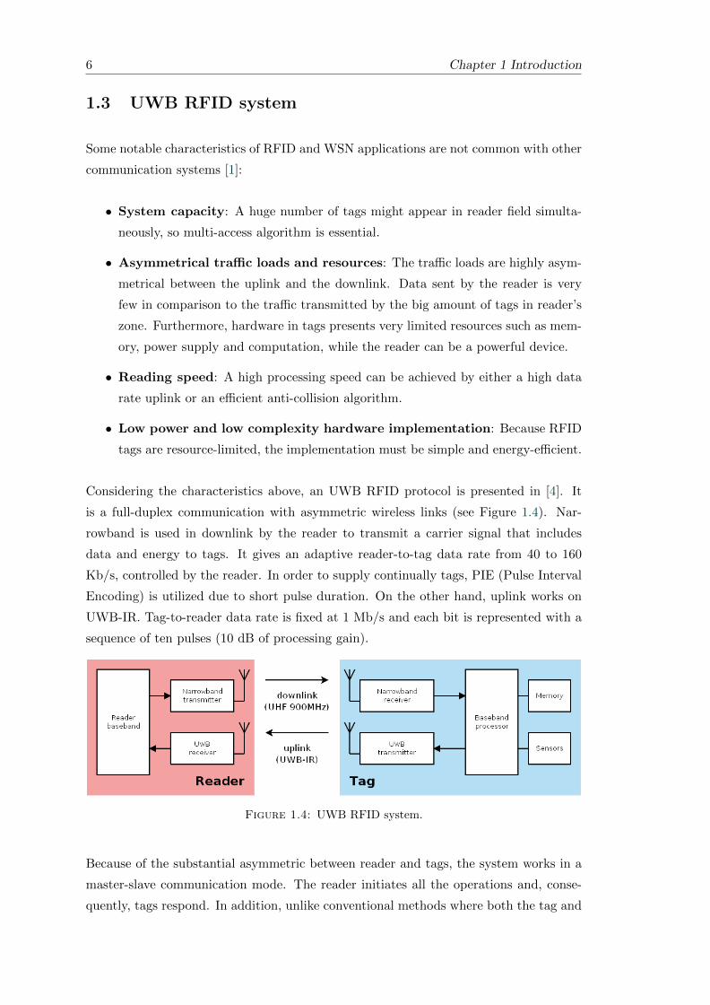
Considering the characteristics above, an UWB RFID protocol is presented in [4]. It
is a full-duplex communication with asymmetric wireless links (see Figure 1.4). Nar-
rowband is used in downlink by the reader to transmit a carrier signal that includes
data and energy to tags. It gives an adaptive reader-to-tag data rate from 40 to 160
Kb/s, controlled by the reader. In order to supply continually tags, PIE (Pulse Interval
Encoding) is utilized due to short pulse duration. On the other hand, uplink works on
UWB-IR. Tag-to-reader data rate is fixed at 1 Mb/s and each bit is represented with a
sequence of ten pulses (10 dB of processing gain).
Figure 1.4: UWB RFID system.
Because of the substantial asymmetric between reader and tags, the system works in a
master-slave communication mode. The reader initiates all the operations and, conse-
quently, tags respond. In addition, unlike conventional methods where both the tag and

Chapter 1 Introduction 7
the reader control data integrity, the proposed protocol handles error checking only in
the reader part. Hence tag implementation is very simple.
1.4 Existing nodes
1.4.1 Intel’s WISP4.1 DL
Intel designed a EPC Global-compliant node called WISP4.1 DL or “Blue WISP”. It is
a passive RFID tag that includes a harvester unit, a 3D-accelerometer, a thermometer
and performs electromagnetic backscattering. Its performance is controlled by a Texas
Instruments MSP430 micro-controller and easily permits its program modification.
It presents a communication range of three meters [10] and is programmed to develop
4-Miller encoding uplink at 256 KHz. It is described in Chapter 3. The following are
some of its features:
Table 1.1: Features of Intel’s WISP4.1 DL.
Micro-controller TI MSP430
Band 900 MHz (ISM)
Modulation ASK
Data rate (Kb/s) 64
Sensors includedThermometer
Accelerometer
Battery needed No
Minimum supply 1.8 V
This device is used as the basis of the UWB RFID tag, taking advantage of its harvester
and micro-controller. And, in order to fulfil the features, a UWB transmitter and a
display are included.
1.4.2 Berkeley’s Mote
The University of California, Berkeley, has been investigating in WSN and creating
devices such as Mote. In fact, they have designed several Mote types such as WeC, Ren,
Dot, Mica and Telos, among others. The following are some of their features:
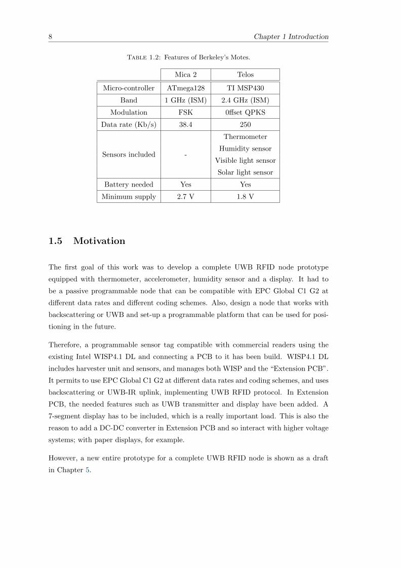
8 Chapter 1 Introduction
Table 1.2: Features of Berkeley’s Motes.
Mica 2 Telos
Micro-controller ATmega128 TI MSP430
Band 1 GHz (ISM) 2.4 GHz (ISM)
Modulation FSK 0ffset QPKS
Data rate (Kb/s) 38.4 250
Sensors included -
Thermometer
Humidity sensor
Visible light sensor
Solar light sensor
Battery needed Yes Yes
Minimum supply 2.7 V 1.8 V
1.5 Motivation
The first goal of this work was to develop a complete UWB RFID node prototype
equipped with thermometer, accelerometer, humidity sensor and a display. It had to
be a passive programmable node that can be compatible with EPC Global C1 G2 at
different data rates and different coding schemes. Also, design a node that works with
backscattering or UWB and set-up a programmable platform that can be used for posi-
tioning in the future.
Therefore, a programmable sensor tag compatible with commercial readers using the
existing Intel WISP4.1 DL and connecting a PCB to it has been build. WISP4.1 DL
includes harvester unit and sensors, and manages both WISP and the “Extension PCB”.
It permits to use EPC Global C1 G2 at different data rates and coding schemes, and uses
backscattering or UWB-IR uplink, implementing UWB RFID protocol. In Extension
PCB, the needed features such as UWB transmitter and display have been added. A
7-segment display has to be included, which is a really important load. This is also the
reason to add a DC-DC converter in Extension PCB and so interact with higher voltage
systems; with paper displays, for example.
However, a new entire prototype for a complete UWB RFID node is shown as a draft
in Chapter 5.
Chapter 1 Introduction 9
1.6 Thesis overview
The content of this work follows a logical structure. First chapters describe the hardware
and the software developed to build this node. After that, measurements on the tag are
compiled. Then, a draft of a new node prototype is created. Finally, conclusions are
done.
These are the chapters:
• Chapter 2 describes the existing Intel WISP4.1 DL which is reused (repro-
grammed) to reach the desired functionality. There are explanations about hard-
ware and software.
• Chapter 3 explains how this “Extension PCB” is designed so as WISP4.1 DL
achieves extra features and shows the way to interconnect both Intel WISP and
Extension PCB. Discussions about the design of the hardware and, specially, the
software are included.
• Chapter 4 gives an overview about all the measurements carried out: reflec-
tion coefficient of the transmission line to the uplink antenna on Extension PCB,
emitted UWB frame shape, current consumption, downlink communication range,
performance tests and harvester’s charging time.
• Chapter 5 is a review, summary and discussion of the development of this work.
Furthermore, there is a description of the future work that should be carried out
on this project.


Chapter 2
Intel WISP4.1 DL
In this chapter, a description of Intel WISP4.1 DL is done. First, its hardware is
explained while showing its power stage, micro-controller and sensors, and afterwards
there is a explanation about the software used to control it.
WISP4.1 DL is a commercial WISP, developed at Intel Research Seattle, that is used as
a basis for the device in this work. It is also called “Blue WISP” and is a whole battery-
free RFID UHF tag which includes 3D-accelerometer and a light and temperature sensor.
Its operating range is up to three meters.
Figure 2.1: Intel WISP4.1 DL, also called “Blue WISP”.
It is a small and light tag and can be reprogrammed in order to accomplish the desired
functionality. All the information about its hardware, proposed software, steps to follow
in order to install firmware, discussion forum and more can be found in “WISP wiki”
[10]. This “wiki” is handled by Intel.
2.1 Hardware
Blue WISP’s hardware can be divided into three blocks: power stage, micro-controller
and sensors (Figure 2.2). See Appendix A for detailed schematics.
11

12 Chapter 2 Intel WISP4.1 DL
Figure 2.2: Block diagram of the Blue WISP.
The “power stage” includes an antenna (λ/2 at 900 MHz) which is thought to be used as
a down and uplink antenna; the uplink uses backscattering. It is followed by a five-stage
harvester; it gets power from the input UHF signal and charges a capacitor that acts as
a power supply. The third part is an ASK demodulator.
In the “micro-controller” block, there is a voltage regulator connected to the main ca-
pacitor of the harvester. It fixes a 1.8 V supply to all the components. Apart from
that, there is a micro-controller to supervise the tag functionality. And, finally, there is
a voltage comparator that sends an interruption to the micro-controller when there is
energy energy stored inside the capacitor.
In the “sensors” block, there are two sensors: a thermometer (LM94021) and an ac-
celerometer (ADXL330). There is also a LED and an electronic switch (TS5A3166).
Sensors are only turned-on just before and during the inspection of their outputs in
order to avoid leakage. The LED is just a visible output for basic tests. Finally, an
electronic switch helps to inspect the voltage level of the battery. Basically, there is an
analog-to-digital converter (ADC) which measures a voltage level, but this value must
be confined between the supply values (0 to 1.8 V). Since the harvester yields a voltage
level up to 5.5 V, it is needed to lower this value to a third part using a voltage divider.
So, this divider is connected/disconnected using the switch to save the energy wasted
when it is not inspected.
Chapter 2 Intel WISP4.1 DL 13
2.2 Software
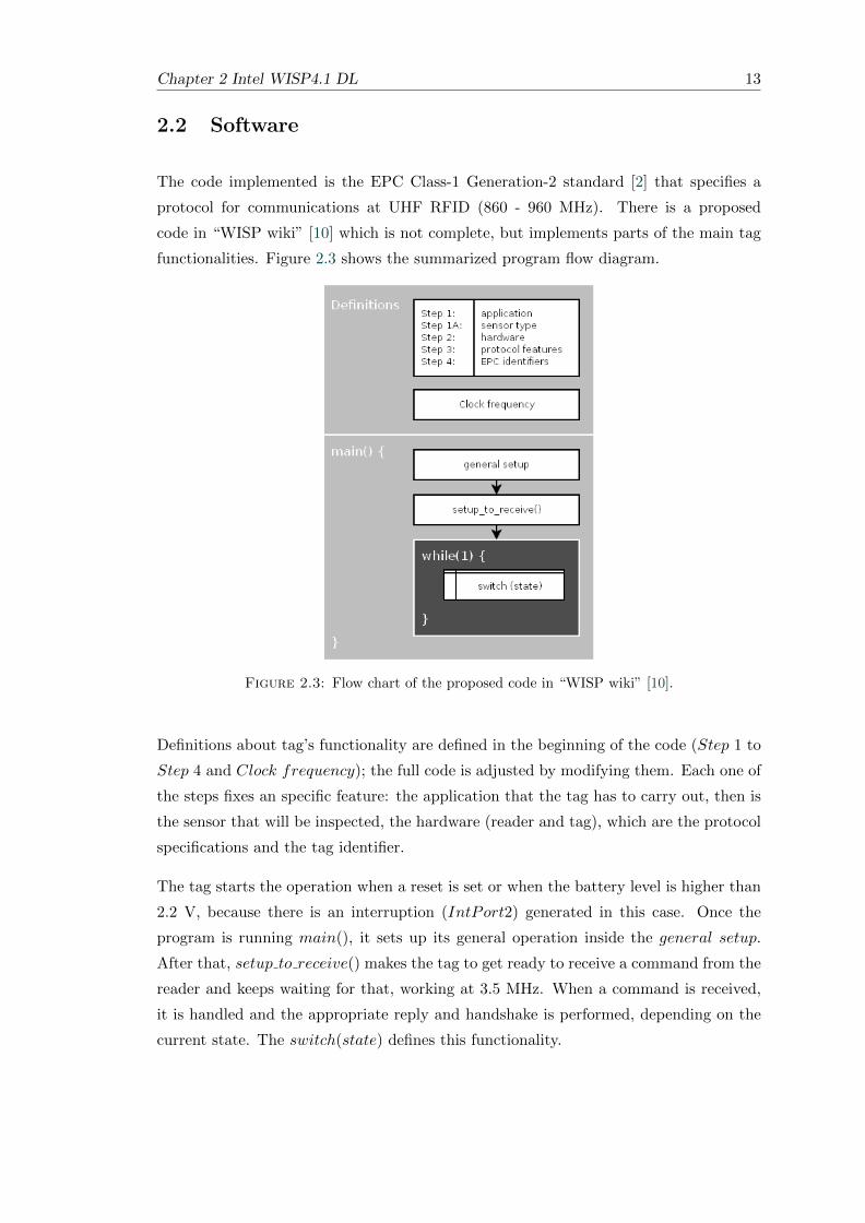
The code implemented is the EPC Class-1 Generation-2 standard [2] that specifies a
protocol for communications at UHF RFID (860 - 960 MHz). There is a proposed
code in “WISP wiki” [10] which is not complete, but implements parts of the main tag
functionalities. Figure 2.3 shows the summarized program flow diagram.
Figure 2.3: Flow chart of the proposed code in “WISP wiki” [10].
Definitions about tag’s functionality are defined in the beginning of the code (Step 1 to
Step 4 and Clock frequency); the full code is adjusted by modifying them. Each one of
the steps fixes an specific feature: the application that the tag has to carry out, then is
the sensor that will be inspected, the hardware (reader and tag), which are the protocol
specifications and the tag identifier.
The tag starts the operation when a reset is set or when the battery level is higher than
2.2 V, because there is an interruption (IntPort2) generated in this case. Once the
program is running main(), it sets up its general operation inside the general setup.
After that, setup to receive() makes the tag to get ready to receive a command from the
reader and keeps waiting for that, working at 3.5 MHz. When a command is received,
it is handled and the appropriate reply and handshake is performed, depending on the
current state. The switch(state) defines this functionality.

14 Chapter 2 Intel WISP4.1 DL
Being the tag in a specific state, it reads the received command and follows the scheme
defined by EPC in the summarized breakdown of switch(state) in Figure 2.4. For ex-
ample, if a tag is in READY state and QUERY command is received, the program
runs the handle query(REPLY ) procedure. Inside this function, the tag checks several
aspects of the command, following EPC description, replies the reader in its turn, ex-
change its state for REPLY and setup to receive() again. After that, the tag jumps
out (break) and go into switch(state) waiting for a new instruction from the reader.
Figure 2.4: Flow chart of the “switch” part of the proposed code.
Going back to receiving part, the way to understand a command from the reader is the
following. In setup to receive(), the tag configures the reception pin (Receive RFID) in
“power stage” block as an interruption (IntPort1) in decreasing edge. It can be seen that
there is a delimiter in preamble in Figure 2.5. The delimiter’s beginning (decreasing
edge) generates an interruption which enables A0 timer and swaps IntPort1 to raising
edge. When the delimiter ends (raising edge), IntPort1 appears again and it stops A0
timer. At this point, A0 timer shows the delimiter’s duration. data − 0, RTcal and
TRcal are calculated following the same steps.
data− 0 is the duration of a ‘0’ bit. Since RTcal equals to data− 0 plus data− 1, the
duration of a ‘1’ bit can be obtained. So, once preamble is received, command can be
Chapter 2 Intel WISP4.1 DL 15
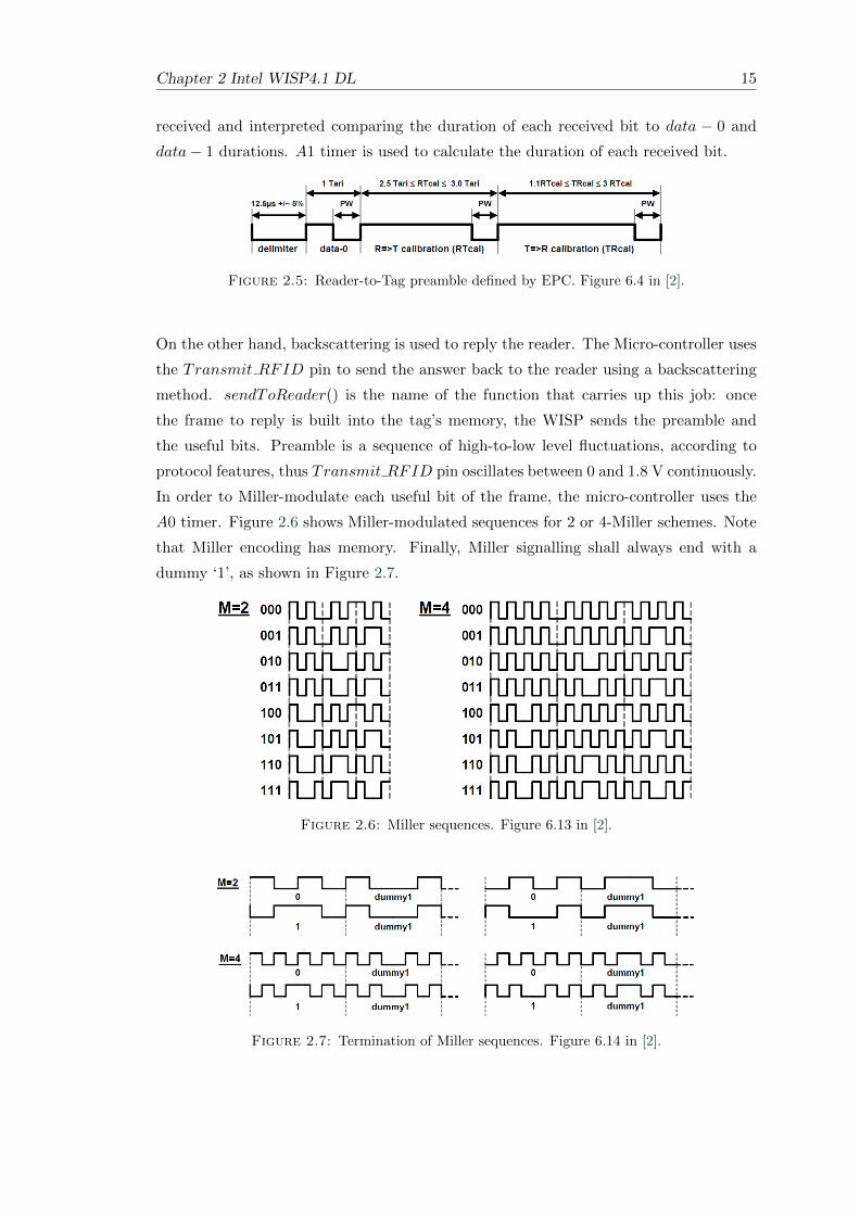
received and interpreted comparing the duration of each received bit to data − 0 and
data− 1 durations. A1 timer is used to calculate the duration of each received bit.
Figure 2.5: Reader-to-Tag preamble defined by EPC. Figure 6.4 in [2].
On the other hand, backscattering is used to reply the reader. The Micro-controller uses
the Transmit RFID pin to send the answer back to the reader using a backscattering
method. sendToReader() is the name of the function that carries up this job: once
the frame to reply is built into the tag’s memory, the WISP sends the preamble and
the useful bits. Preamble is a sequence of high-to-low level fluctuations, according to
protocol features, thus Transmit RFID pin oscillates between 0 and 1.8 V continuously.
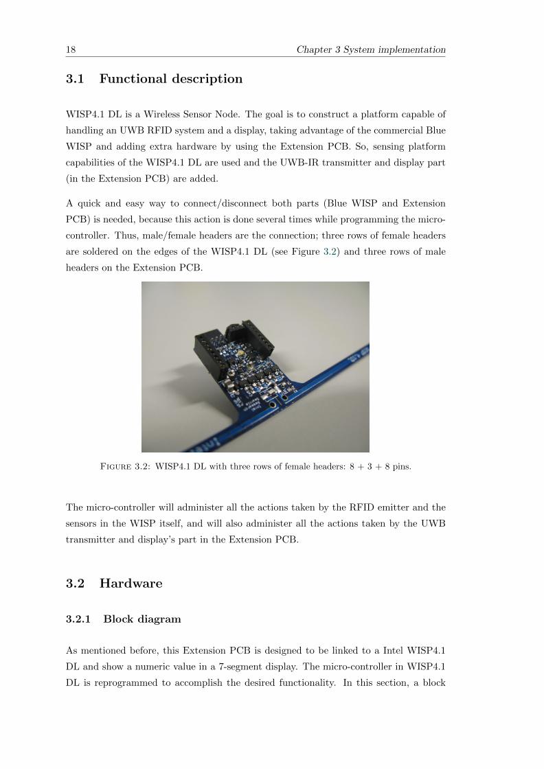
In order to Miller-modulate each useful bit of the frame, the micro-controller uses the
A0 timer. Figure 2.6 shows Miller-modulated sequences for 2 or 4-Miller schemes. Note
that Miller encoding has memory. Finally, Miller signalling shall always end with a
dummy ‘1’, as shown in Figure 2.7.
Figure 2.6: Miller sequences. Figure 6.13 in [2].
Figure 2.7: Termination of Miller sequences. Figure 6.14 in [2].

16 Chapter 2 Intel WISP4.1 DL
The clock frequency is changed to 3 MHz only when the tag is replying to the reader.
Moreover, at any time within the program, if the battery level is not enough to supply
the tag, the program stops and activates IntPort2. The tag wakes up again when the
battery level is above 2.2 V.
Finally, in order to download the built code into the Blue WISP a debugger is needed.
See “Getting started” ⇒ “Programming the WISP” in “WISP wiki” [10] for more in-
formation. The debugger used is a USB Key Debugger (Figure 2.8).
Figure 2.8: Texas Instruments’ eZ430-F2013 USB debugger connected to WISP4.1DL.

Chapter 3
System implementation
This chapter talks about the design of the “Extension PCB” (Figure 3.1) that will be
connected to Intel’s WISP4.1 DL. To explain all the content, the description is separated
into three sections: functional description, hardware and software.
Figure 3.1: Perspective view of the Extension PCB.
Firstly, the “functional description” section explains which are the targets of this PCB,
while describing which parts of WISP4.1 DL are used, how it is connected to the Ex-
tension PCB and what is included in this PCB to achieve those aims. Afterwards, the
“hardware” section describes the schematic designed, while explaining the reason of each
component and the global interaction. Finally, the “software” section explains the mod-
ifications and the additions to the original code, while describing the three operating
modes defined.
17
18 Chapter 3 System implementation
3.1 Functional description
WISP4.1 DL is a Wireless Sensor Node. The goal is to construct a platform capable of
handling an UWB RFID system and a display, taking advantage of the commercial Blue
WISP and adding extra hardware by using the Extension PCB. So, sensing platform
capabilities of the WISP4.1 DL are used and the UWB-IR transmitter and display part
(in the Extension PCB) are added.
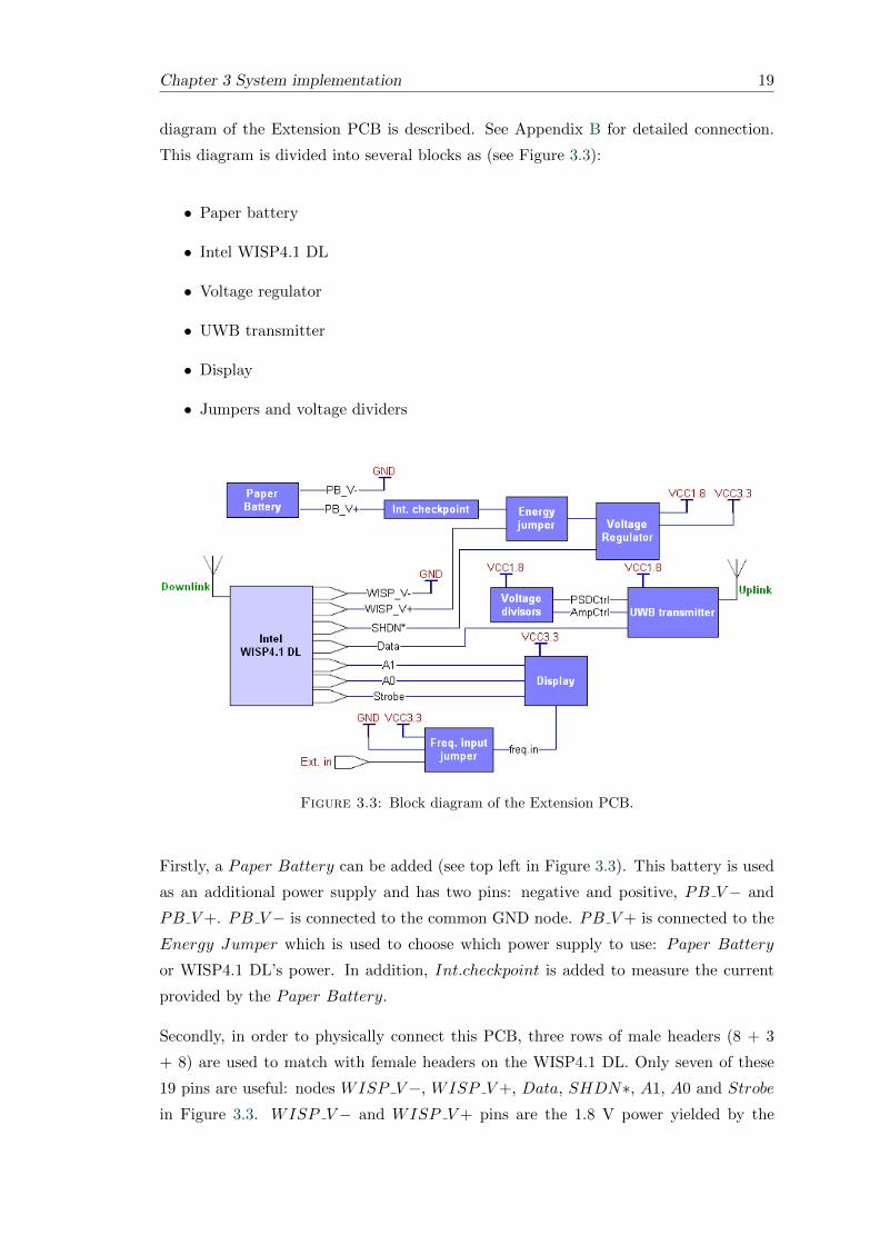
A quick and easy way to connect/disconnect both parts (Blue WISP and Extension
PCB) is needed, because this action is done several times while programming the micro-
controller. Thus, male/female headers are the connection; three rows of female headers
are soldered on the edges of the WISP4.1 DL (see Figure 3.2) and three rows of male
headers on the Extension PCB.
Figure 3.2: WISP4.1 DL with three rows of female headers: 8 + 3 + 8 pins.
The micro-controller will administer all the actions taken by the RFID emitter and the
sensors in the WISP itself, and will also administer all the actions taken by the UWB
transmitter and display’s part in the Extension PCB.
3.2 Hardware
3.2.1 Block diagram
As mentioned before, this Extension PCB is designed to be linked to a Intel WISP4.1
DL and show a numeric value in a 7-segment display. The micro-controller in WISP4.1
DL is reprogrammed to accomplish the desired functionality. In this section, a block
Chapter 3 System implementation 19
diagram of the Extension PCB is described. See Appendix B for detailed connection.
This diagram is divided into several blocks as (see Figure 3.3):
• Paper battery
• Intel WISP4.1 DL
• Voltage regulator
• UWB transmitter
• Display
• Jumpers and voltage dividers
Figure 3.3: Block diagram of the Extension PCB.
Firstly, a Paper Battery can be added (see top left in Figure 3.3). This battery is used
as an additional power supply and has two pins: negative and positive, PB V− and
PB V+. PB V− is connected to the common GND node. PB V+ is connected to the
Energy Jumper which is used to choose which power supply to use: Paper Battery
or WISP4.1 DL’s power. In addition, Int.checkpoint is added to measure the current
provided by the Paper Battery.
Secondly, in order to physically connect this PCB, three rows of male headers (8 + 3
+ 8) are used to match with female headers on the WISP4.1 DL. Only seven of these
19 pins are useful: nodes WISP V−, WISP V+, Data, SHDN∗, A1, A0 and Strobe
in Figure 3.3. WISP V− and WISP V+ pins are the 1.8 V power yielded by the
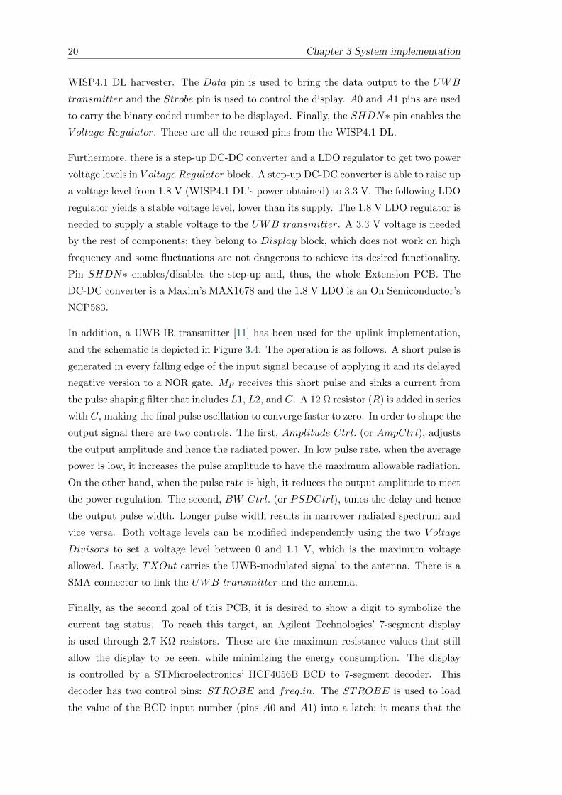
20 Chapter 3 System implementation
WISP4.1 DL harvester. The Data pin is used to bring the data output to the UWB
transmitter and the Strobe pin is used to control the display. A0 and A1 pins are used
to carry the binary coded number to be displayed. Finally, the SHDN∗ pin enables the
V oltage Regulator. These are all the reused pins from the WISP4.1 DL.
Furthermore, there is a step-up DC-DC converter and a LDO regulator to get two power
voltage levels in V oltage Regulator block. A step-up DC-DC converter is able to raise up
a voltage level from 1.8 V (WISP4.1 DL’s power obtained) to 3.3 V. The following LDO
regulator yields a stable voltage level, lower than its supply. The 1.8 V LDO regulator is
needed to supply a stable voltage to the UWB transmitter. A 3.3 V voltage is needed
by the rest of components; they belong to Display block, which does not work on high
frequency and some fluctuations are not dangerous to achieve its desired functionality.
Pin SHDN∗ enables/disables the step-up and, thus, the whole Extension PCB. The
DC-DC converter is a Maxim’s MAX1678 and the 1.8 V LDO is an On Semiconductor’s
NCP583.
In addition, a UWB-IR transmitter [11] has been used for the uplink implementation,
and the schematic is depicted in Figure 3.4. The operation is as follows. A short pulse is
generated in every falling edge of the input signal because of applying it and its delayed
negative version to a NOR gate. MF receives this short pulse and sinks a current from
the pulse shaping filter that includes L1, L2, and C. A 12 Ω resistor (R) is added in series
with C, making the final pulse oscillation to converge faster to zero. In order to shape the
output signal there are two controls. The first, Amplitude Ctrl. (or AmpCtrl), adjusts
the output amplitude and hence the radiated power. In low pulse rate, when the average
power is low, it increases the pulse amplitude to have the maximum allowable radiation.
On the other hand, when the pulse rate is high, it reduces the output amplitude to meet
the power regulation. The second, BW Ctrl. (or PSDCtrl), tunes the delay and hence
the output pulse width. Longer pulse width results in narrower radiated spectrum and
vice versa. Both voltage levels can be modified independently using the two V oltage
Divisors to set a voltage level between 0 and 1.1 V, which is the maximum voltage
allowed. Lastly, TXOut carries the UWB-modulated signal to the antenna. There is a
SMA connector to link the UWB transmitter and the antenna.
Finally, as the second goal of this PCB, it is desired to show a digit to symbolize the
current tag status. To reach this target, an Agilent Technologies’ 7-segment display
is used through 2.7 KΩ resistors. These are the maximum resistance values that still
allow the display to be seen, while minimizing the energy consumption. The display
is controlled by a STMicroelectronics’ HCF4056B BCD to 7-segment decoder. This
decoder has two control pins: STROBE and freq.in. The STROBE is used to load
the value of the BCD input number (pins A0 and A1) into a latch; it means that the

Chapter 3 System implementation 21
Figure 3.4: Schematic of the UWB transmitter. Figure 1a in [11].
valid input number does not have to be set continuously. On the other hand, freq.in
adjusts display-frequency input. It means that the selected segment outputs will be
high or low depending on this input. In fact, the segment output is a shifted NOR gate
applied to freq.in and to each of the theoretical segment outputs. In order to control
freq.in, Freq.in jumper is added and allows to insert an external input. Both pins,
STROBE and freq.in, are useful to save energy.
See schematic in Appendix B for specific connection details and layout images.
3.2.2 Physical connection
The Intel WISP is connected to the PCB with headers. In Figure 3.5 you can see the
“plugged” tag. They are connected by three rows of headers (8 + 3 + 8) which means
an amount of 19 pins.
Figure 3.5: Blue WISP connected to Extension PCB.

22 Chapter 3 System implementation
In order to operate the UWB transmitter, some pins are needed to control this hardware.
Firstly, the supply is obtained from the 1.8 V LDO. The amplitude control (AmpCtrl)
and power spectral density control (PSDCtrl) are the middle pins of two potentiometers,
that give an adjustable level from 0 to 1.0 V. One of the available pins in the three rows
on WISP4.1’s borders, called Data, sends the coded frame from the µC to the UWB
transmitter, which modulates this frame (see Data pin Appendix B). Finally, the output
of the UWB transmitter is the TXout pin that transfers the signal to the antenna
through a 50 Ω transmission line.
Furthermore, five pins are needed to control the 7-segment and its decoder for 16 different
values (four data pins and one control pin), but only three are available. That is why
only two data pins can be used, giving only four different values. The control pin is
called Strobe and it controls the latch; when the data is ready, it gives the command to
load the value into the decoder. Data pins are A0 and A1. However, a non-consumption
point is needed, the theoretical A2 and A3 are connected to V3.3 and A0, respectively,
since that 1111b shows nothing on the 7-segment display. This last connection is really
important; if there is some LED of the display trying to turn on, while the Blue WISP
is charging, it will never be able to start.
3.3 Software
Intel WISP4.1 DL uses the proposed code in “WISP wiki” [10] which is described in
Chapter 2. In this section, there is a description of how this code has been adapted
to match the reader and three operating modes (opModes) are defined to accomplish
different functionalities.
Figure 3.6 shows the modified diagram of the program flow, in comparison to the pro-
posed code (Figure 2.3). The general functionality of the tag starts when it wakes
up because of IntPort2 interruption and does some settings in general setup. If
OpMode 3 is chosen, the tag executes UWB RFID functionality by entering into the
UWB main loop(). Otherwise, the tag gets ready to receive a command from the reader
in setup to receive() and enters into the switch(state). Inside the switch(state), the
tag receives a command from the reader and acts properly depending on the current
status. This last part differs from the proposed code, because a different functionality
is added to accomplish OpMode 2. After the work is done, the tag gets ready again to
receive a new instruction.
Note that the modified parts are coloured in blue and the added ones are in green. In
Definitions, Step0 is added to select the operating mode. Clock frequency is modified
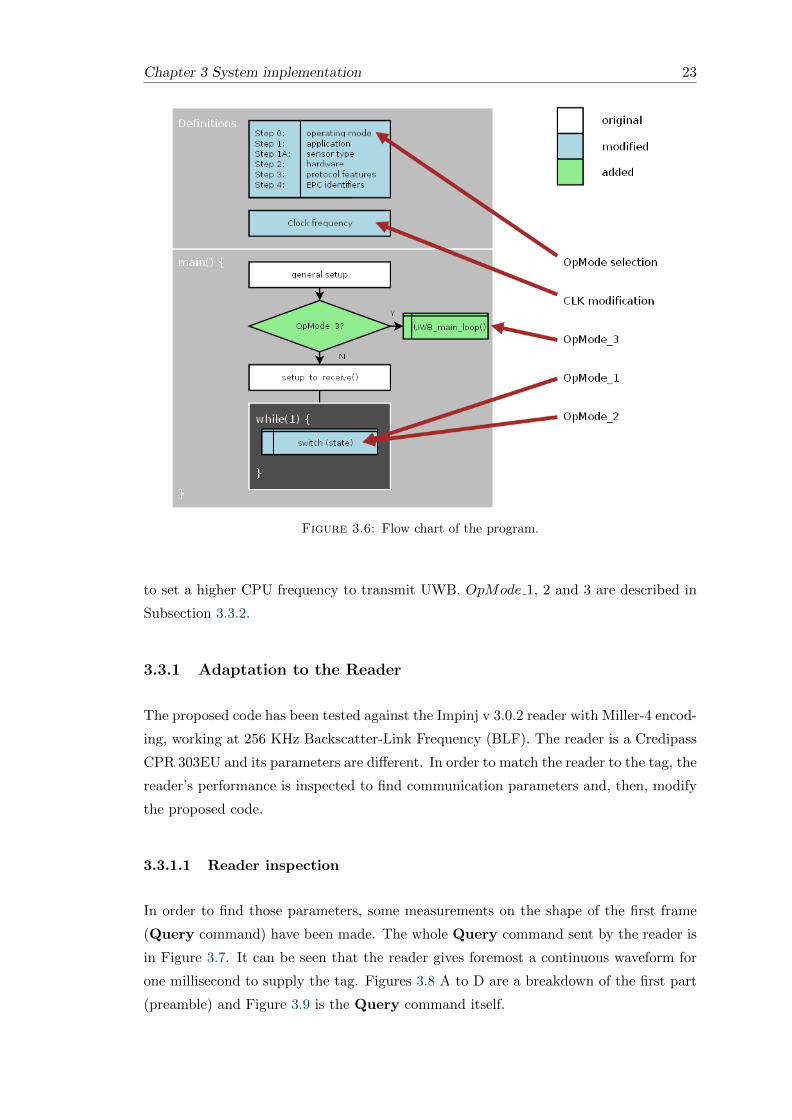
Chapter 3 System implementation 23
Figure 3.6: Flow chart of the program.
to set a higher CPU frequency to transmit UWB. OpMode 1, 2 and 3 are described in
Subsection 3.3.2.
3.3.1 Adaptation to the Reader
The proposed code has been tested against the Impinj v 3.0.2 reader with Miller-4 encod-
ing, working at 256 KHz Backscatter-Link Frequency (BLF). The reader is a Credipass
CPR 303EU and its parameters are different. In order to match the reader to the tag, the
reader’s performance is inspected to find communication parameters and, then, modify
the proposed code.
3.3.1.1 Reader inspection
In order to find those parameters, some measurements on the shape of the first frame
(Query command) have been made. The whole Query command sent by the reader is
in Figure 3.7. It can be seen that the reader gives foremost a continuous waveform for
one millisecond to supply the tag. Figures 3.8 A to D are a breakdown of the first part
(preamble) and Figure 3.9 is the Query command itself.

24 Chapter 3 System implementation
Figure 3.7: Query command sent by reader.
Figure 3.8: Breakdown of the Query command’s preamble. Figures on top: A, B;bottom: C, D.
Since command’s preamble defined by EPC is shown in Figure 2.5, Figures 3.8 A to D
are: delimiter, data − 0 (Tari), RTcal and TRcal, respectively, and their time values
are 14.4, 24, 66.4 and 144 µs. EPC Class-1 Generation-2 protocol [2] defines delimiter
as a fixed value for any configuration. Tari equals to data− 0 length and RTcal equals
to data− 0 plus data− 1 length. And TRcal defines BLF in Equation (3.1).
BLF =DR
TRcal(3.1)
where DR is a parameter defined also by the reader, that can be 8 or 64/3. As described
in Figure 3.10, a Query command frame is: Command, DR, M, TRext, Sel, Session,

Chapter 3 System implementation 25
Figure 3.9: Last part of the Query command.
Target, Q and CRC-5. From Figure 3.9, it can interpreted that the Query command
bits are: 1000 0 01 1 00 00 0 0000 10101, which mean:
Figure 3.10: Query command definition. Table 6.21 in [2].
• Command = Query
• DR = 8
• M = 2. 2-Miller encoding
• TRext = 1. Long Tag-to-Reader preamble (Figure 6.15 in [2])
• Sel = All
• Session = S0
• Target = A
• Q = 0
• CRC-5 = 10101b
In this case, reader sets DR bit to zero, thus DR = 8. Using equation (3.1), the resulting
BLF is 55.56 KHz. M bits are set to 01b what means that 2-Miller encoding is used.
In conclusion, BLF needs to be slowed down from 256 to 56 KHz, and mutate from 4 to
2-Miller encoding.

26 Chapter 3 System implementation
3.3.1.2 Clock modification
The WISP’s µC has a system clock that feeds several blocks. A Clock System Control
administers this clock to Master clock (MCLK) and Sub-main clock (SMCLK). In this
case, MCLK feeds the CPU and SMCLK feeds a timer. When this timer (or counter)
reaches its target value, it toggles the output in order to build the modulation and starts
to count again from zero.
The operation methodology in the proposed code was, basically, as follows:
• First, the system clock is fixed to 3 MHz, like SMCLK (timer), and MCLK is set
to 1.5 MHz.
• Then, the target value of the timer is set to 6, as the default value. It means that,
unless there is a modification on the target value, the output will be a square wave.
Since the target value is 6, the output will be toggled every six SMCLK-periods
(2 µs); thus, it is 256 KHz BLF.
• At the same time, the CPU processes the bits that are about to be sent. Depending
on the current bit and according to Miller encoding, CPU changes the target value
of the timer to 12 and, immediately later, sets it again to 6. It will build a long
pulse (4 µs) in between short pulses. See Figure 2.6.
• Finally, when all the bits are transmitted, the timer is disabled.
The system clock must be fixed to 12 times the value of BLF in order to reach the desired
BLF. So, in order to reach 55.56 KHz of BLF, the system clock is fixed to 666.67 KHz.
On the other hand, 2-Miller encoding might be developed, in spite of 4-Miller. It means
that the bit-rate raises up from BLF/4 to BLF/2 (∼ 28 Kb/s). Thus, each bit has to
be processed twice faster. Taking advantage of the code, it is only needed to double the
MCLK (CPU); hence both clocks (MCLK and SMCLK) are set to 666.67 KHz.
These modifications are done in the block Clock frequency (Figure 3.6) that consists of
several macros. In Figure 3.11, the SEND CLOCK macro redefines the system clock
to 666 KHz, in spite of 3 MHz (commented code). There is, in addition, a macro called
SEND CLOCK UWB which defines the clock in 10 MHz. The program applies either
the first or the second macro depending on which is the operating mode chosen. This
idea is described in the following subsection.
At this point, the code is transmitting at 55.56 KHz BLF and using 2-Miller encoding.
Still, there are some problems on timing and synchronism and have been corrected. To
be precise, in some points during the transmission, the proposed code does not spend
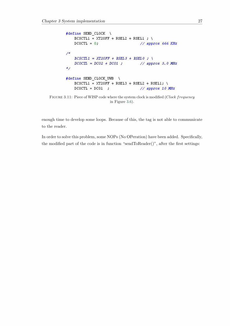
Chapter 3 System implementation 27
Figure 3.11: Piece of WISP code where the system clock is modified (Clock frequencyin Figure 3.6).
enough time to develop some loops. Because of this, the tag is not able to communicate
to the reader.
In order to solve this problem, some NOPs (No OPeration) have been added. Specifically,
the modified part of the code is in function “sendToReader()”, after the first settings:
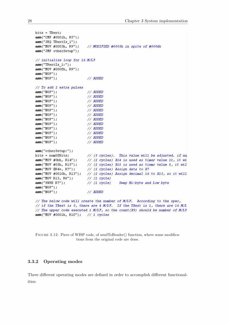
28 Chapter 3 System implementation
Figure 3.12: Piece of WISP code, of sendToReader() function, where some modifica-tions from the original code are done.
3.3.2 Operating modes
Three different operating modes are defined in order to accomplish different functional-
ities:
Chapter 3 System implementation 29
• OpMode 1: EPC Class-1 Generation-2
• OpMode 2: UWB test
• OpMode 3: UWB RFID
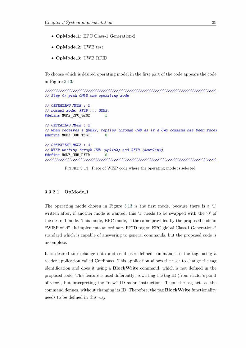
To choose which is desired operating mode, in the first part of the code appears the code
in Figure 3.13:
Figure 3.13: Piece of WISP code where the operating mode is selected.
3.3.2.1 OpMode 1
The operating mode chosen in Figure 3.13 is the first mode, because there is a ‘1’
written after; if another mode is wanted, this ‘1’ needs to be swapped with the ‘0’ of
the desired mode. This mode, EPC mode, is the same provided by the proposed code in
“WISP wiki”. It implements an ordinary RFID tag on EPC global Class-1 Generation-2
standard which is capable of answering to general commands, but the proposed code is
incomplete.
It is desired to exchange data and send user defined commands to the tag, using a
reader application called Credipass. This application allows the user to change the tag
identification and does it using a BlockWrite command, which is not defined in the
proposed code. This feature is used differently: rewriting the tag ID (from reader’s point
of view), but interpreting the “new” ID as an instruction. Then, the tag acts as the
command defines, without changing its ID. Therefore, the tag BlockWrite functionality
needs to be defined in this way.

30 Chapter 3 System implementation
The Figure 3.14 shows the new flow chart of switch(state) code. It can be seen (in green)
that SECURED state, its handle() functions and a special contemplation for Op-
Mode 2 (OpMode 2 activity()) are added. Taking advantage from the already written
code, the code which identifies a received BlockWrite command has been programmed.
Figure 3.14: Flow chart of the “switch” part of the program.
It is important to know that a tag ID is 16 bytes long (Figure 3.15): protocol control
(2 bytes), ID body (12 bytes) and 16-CRC (2 bytes). Obviously, all 16 bytes need to
be send and Credipass application does it by sending 8 two-byte-long commands. Thus,
the tag needs to wait for all the 8 commands before acting in any way. Once the full
“new” tag ID is received, the tag reads its bits and will proceed in the defined way.
There are 12 useful bytes (ID body) and an instruction is defined as a command (2
bytes), a parameter (2 bytes) and useless bits (8 bytes). The command collection is:
• wDisp: Writes the number received as a parameter into to display’s memory,
which will be shown when the display is turned on.
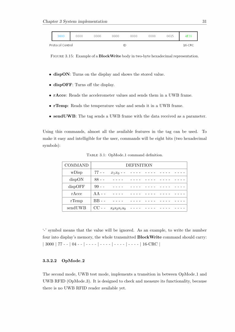
Chapter 3 System implementation 31
Figure 3.15: Example of a BlockWrite body in two-byte hexadecimal representation.
• dispON: Turns on the display and shows the stored value.
• dispOFF: Turns off the display.
• rAcce: Reads the accelerometer values and sends them in a UWB frame.
• rTemp: Reads the temperature value and sends it in a UWB frame.
• sendUWB: The tag sends a UWB frame with the data received as a parameter.
Using this commands, almost all the available features in the tag can be used. To
make it easy and intelligible for the user, commands will be eight bits (two hexadecimal
symbols):
Table 3.1: OpMode 1 command definition.
COMMAND DEFINITION
wDisp 77 - - x1x0 - - - - - - - - - - - - - - - - - -
dispON 88 - - - - - - - - - - - - - - - - - - - - - -
dispOFF 99 - - - - - - - - - - - - - - - - - - - - - -
rAcce AA - - - - - - - - - - - - - - - - - - - - - -
rTemp BB - - - - - - - - - - - - - - - - - - - - - -
sendUWB CC - - s3s2s1s0 - - - - - - - - - - - - - - - -
‘-’ symbol means that the value will be ignored. As an example, to write the number
four into display’s memory, the whole transmitted BlockWrite command should carry:
| 3000 | 77 - - | 04 - - | - - - - | - - - - | - - - - | - - - - | 16-CRC |
3.3.2.2 OpMode 2
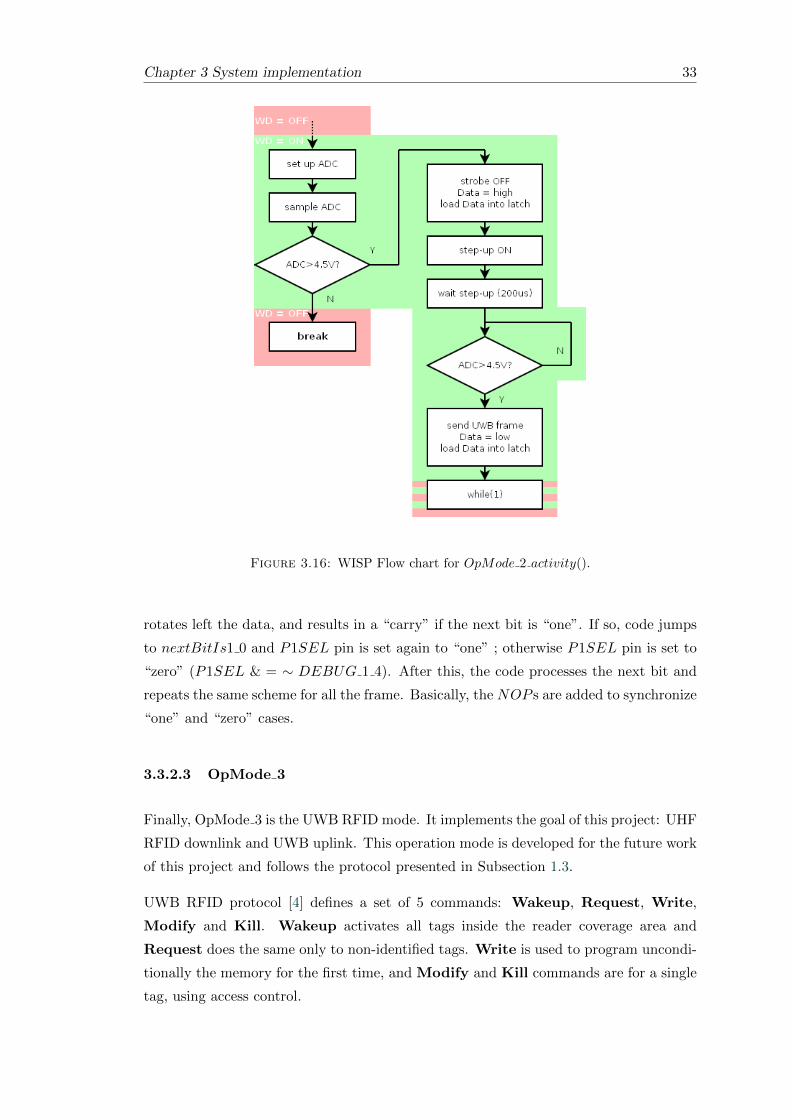
The second mode, UWB test mode, implements a transition in between OpMode 1 and
UWB RFID (OpMode 3). It is designed to check and measure its functionality, because
there is no UWB RFID reader available yet.

32 Chapter 3 System implementation
Its global algorithm (OpMode 2 activity()) can be seen in Figure 3.16. After the re-
ceived Query command, it inspects the power, sampling an Analog-to-Digital Converter
(ADC). If the power voltage is higher than 4.5 V, tag saves 11b value into the Display
latch and turns on the DC-DC step-up converter; at this point, the latch value is 1111b
that means that there is nothing to display (see Table 3.2), so there is no power con-
sumption. The program also deactivates all the interruptions and activates a Watchdog
timer (WD = ON, green background color), which resets µC after a certain time just
in case it gets stuck. Afterwards, it waits 200 µs (because of the power-up response
of step-up) and waits again until the accumulator level is over 4.5 V. Then, it sends
an 18-bit-long UWB frame (1-bit header + 16-bit body + 1-bit ending). Afterwards,
it saves 00b into latch and switches on display (showing the number ‘4’) until it runs
out of battery. Note that, whichever other command is received, there is no activity.
Moreover, the display’s value can be changed depending on the application.
Table 3.2: Relation between data pins and its display equivalence, because of physicalconnection.
DATA VALUE OF DISPLAY’S LATCH DISPLAYA1 A0 B3 B2 B1 B0 CHARACTER
0 0 0 1 0 0 40 1 0 1 0 1 51 0 1 1 1 0 -1 1 1 1 1 1 BLANK
Note that, in while(1), the µC switches on and off the WD timer (green and red back-
ground color). It is done to control periodically the program status.
The Data pin is the cable that brings the output signal to the UWB transmitter. It
needs a high frequency output; however, the maximum µC’s clock frequency is about 16
MHz. Thus, to develop an On-Off Keying (OOK), the µC clock signal is sent directly
to the UWB transmitter to transmit a logic “one”, and no signal to transmit a “zero”.
The clock has been adjusted to 10 MHz (Figure 3.11) based on the proposed UWB RFID
protocol [4]. An output signal of 10 MHz equals to 1 Mb/s communication, because each
“one” bit is modulated as 10 pulses (processing gain of 10 dBs).
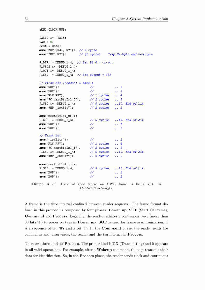
Note that only specific pins of the µC are able to bring the clock signal. Figure 3.17 shows
a part of the code that sends the clock to the UWB transmitter. Firstly, system clock
is set to 10 Mhz in SEND CLOCK UWB macro. Afterwards, timers’ interruptions
are disabled and 16-bit data is loaded into R7 register. The following block of four
commands sets the P1.4 pin as an output, and establishes the system clock as the output
wave (P1SEL | = DEBUG 1 4) because header bit is “one”. After two program cycles
(NOP equals to one cycle), the tag gets ready for the first bit of the frame: RLC R7
Chapter 3 System implementation 33
Figure 3.16: WISP Flow chart for OpMode 2 activity().
rotates left the data, and results in a “carry” if the next bit is “one”. If so, code jumps
to nextBitIs1 0 and P1SEL pin is set again to “one” ; otherwise P1SEL pin is set to
“zero” (P1SEL & = ∼ DEBUG 1 4). After this, the code processes the next bit and
repeats the same scheme for all the frame. Basically, the NOP s are added to synchronize
“one” and “zero” cases.
3.3.2.3 OpMode 3
Finally, OpMode 3 is the UWB RFID mode. It implements the goal of this project: UHF
RFID downlink and UWB uplink. This operation mode is developed for the future work
of this project and follows the protocol presented in Subsection 1.3.
UWB RFID protocol [4] defines a set of 5 commands: Wakeup, Request, Write,
Modify and Kill. Wakeup activates all tags inside the reader coverage area and
Request does the same only to non-identified tags. Write is used to program uncondi-
tionally the memory for the first time, and Modify and Kill commands are for a single
tag, using access control.
34 Chapter 3 System implementation
Figure 3.17: Piece of code where an UWB frame is being sent, inOpMode 2 activity().
A frame is the time interval confined between reader requests. The frame format de-
fined in this protocol is composed by four phases: Power up, SOF (Start Of Frame),
Command and Process. Logically, the reader radiates a continuous wave (more than
30 bits ‘1’) to power on tags in Power up. SOF is used for frame synchronization; it
is a sequence of ten ‘0’s and a bit ‘1’. In the Command phase, the reader sends the
commands and, afterwards, the reader and the tag interact in Process.
There are three kinds of Process. The primer kind is TX (Transmitting) and it appears
in all valid operations. For example, after a Wakeup command, the tags transmit their
data for identification. So, in the Process phase, the reader sends clock and continuous

Chapter 3 System implementation 35
bit ‘1’ for tags’ initialization (load data from memory, generate pseudo-random number
PN code, ...). After a start bit ‘0’, tags transmit data based on PN code. Also, RX
(Receiving) Process is used in Write and Modify commands, and sets data in tags’
memory using a MSB-first data format. In order to differ SOF from data, each data
byte is delimited by a start bit (‘0’) and a stop bit (‘1’). The third kind of Process is
CMP (Comparing). It is only used in Modify or Kill commands: tags compare their
own ID to data broadcasted by the reader (bit by bit) and only a unique tag executes
the command.
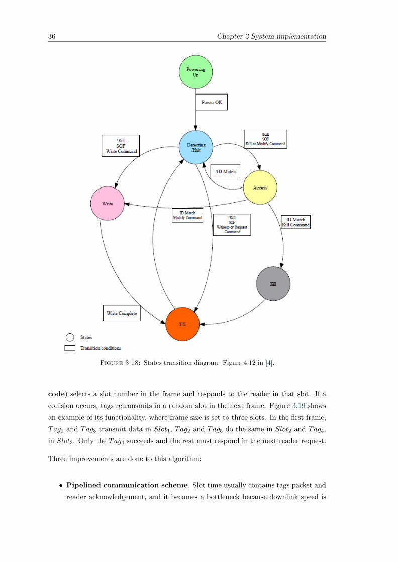
Other items defined in this protocol are the flags and the states. Tags indicate their
current status on three control flags: ACK (indicates that tag has been identified),
NAK (is a N-bit counter and increases by one for each failed transmission) and Kill
(identifies a killed tag). These flags are set while the states are switched. Six states are
defined in this protocol and follow the transition diagram in Figure 3.18:
• Powering Up: Scavenging unites in tags capture the energy from the electro-
magnetic signal and store it in an accumulator (capacitor).
• Detecting/Halt: This is the initial state of every powered tag. Tags are detecting
incoming signals in this state, while capturing SOF and Command. After this
state, tags enter a new frame to execute the corresponding operation.
• Transmitting: Firstly, tag loads data into cache and generates a PN code.
Secondly, the slot counter in the tag counts down PN code until it reaches zero.
Finally, the tag sends data and keeps waiting for reader’s ACK or NAK.
• Writing: Tag programs its memory by receiving data from reader.
• Accessing: It happens just before an operation to a specific tag (Modify or Kill).
Tag compares its ID to the incoming signal bit by bit, and can be interrupted by
any different bit. Only one tag with the same data completes the state.
• Kill: It sets the Kill flag to permanently disable the tag.
Since there is a big amount of tags attempting to communicate to the reader, an anti-
collision method is needed. A collision occurs when more than one tag occupies the same
RF communication channel simultaneously. Since this is a multiple-tag environment,
system needs a multiple-access scheme (anti-collision algorithm) that allows reader to
request data from several tags.
The algorithm chosen by the proposed UWB RFID protocol in [4] is framed slotted
ALOHA, where a frame consists of a number of slots. Basically, a tag randomly (PN
36 Chapter 3 System implementation
Figure 3.18: States transition diagram. Figure 4.12 in [4].
code) selects a slot number in the frame and responds to the reader in that slot. If a
collision occurs, tags retransmits in a random slot in the next frame. Figure 3.19 shows
an example of its functionality, where frame size is set to three slots. In the first frame,
Tag1 and Tag3 transmit data in Slot1, Tag2 and Tag5 do the same in Slot2 and Tag4,
in Slot3. Only the Tag4 succeeds and the rest must respond in the next reader request.
Three improvements are done to this algorithm:
• Pipelined communication scheme. Slot time usually contains tags packet and
reader acknowledgement, and it becomes a bottleneck because downlink speed is
Chapter 3 System implementation 37
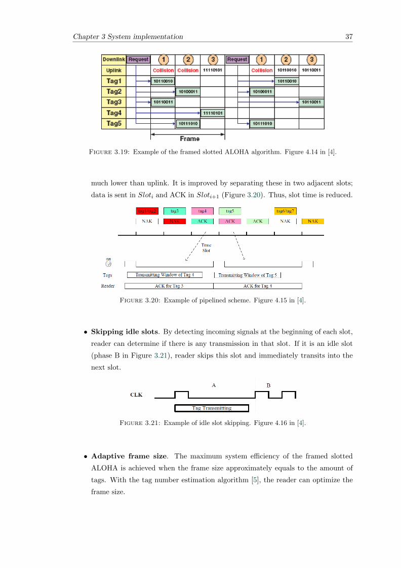
Figure 3.19: Example of the framed slotted ALOHA algorithm. Figure 4.14 in [4].
much lower than uplink. It is improved by separating these in two adjacent slots;
data is sent in Sloti and ACK in Sloti+1 (Figure 3.20). Thus, slot time is reduced.
Figure 3.20: Example of pipelined scheme. Figure 4.15 in [4].
• Skipping idle slots. By detecting incoming signals at the beginning of each slot,
reader can determine if there is any transmission in that slot. If it is an idle slot
(phase B in Figure 3.21), reader skips this slot and immediately transits into the
next slot.
Figure 3.21: Example of idle slot skipping. Figure 4.16 in [4].
• Adaptive frame size. The maximum system efficiency of the framed slotted
ALOHA is achieved when the frame size approximately equals to the amount of
tags. With the tag number estimation algorithm [5], the reader can optimize the
frame size.
38 Chapter 3 System implementation
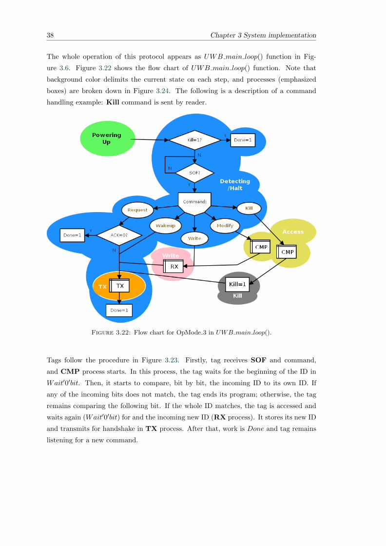
The whole operation of this protocol appears as UWB main loop() function in Fig-
ure 3.6. Figure 3.22 shows the flow chart of UWB main loop() function. Note that
background color delimits the current state on each step, and processes (emphasized
boxes) are broken down in Figure 3.24. The following is a description of a command
handling example: Kill command is sent by reader.
Figure 3.22: Flow chart for OpMode 3 in UWB main loop().
Tags follow the procedure in Figure 3.23. Firstly, tag receives SOF and command,
and CMP process starts. In this process, the tag waits for the beginning of the ID in
Wait′0′bit. Then, it starts to compare, bit by bit, the incoming ID to its own ID. If
any of the incoming bits does not match, the tag ends its program; otherwise, the tag
remains comparing the following bit. If the whole ID matches, the tag is accessed and
waits again (Wait′0′bit) for and the incoming new ID (RX process). It stores its new ID
and transmits for handshake in TX process. After that, work is Done and tag remains
listening for a new command.

Chapter 3 System implementation 39
Figure 3.23: Kill command functionality.
Figure 3.24: Flow chart of TX (A), RX (B) and CMP (C) processes.


Chapter 4
Measurements
In this chapter, a summary of the measurements on Extension PCB linked to Blue
WISP is written. These measurements are done to check and inspect Extension PCB’s
functionality and the system capabilities. Six measurement have been performed:
• Reflection coefficient, S11, of the transmission line to the uplink antenna
• Shape of an UWB pulse
• Current consumption
• Communication range (downlink)
• Performance tests
• Harvester’s charging time
Table 4.1 explains the system characteristics in each measurement and Table 4.2 de-
scribes general reader conditions. In addition, there is a summary of the measurements
results and specifications in Section 4.7.
All the data collected and measurements procedure in the laboratory are described in
Appendix C.
4.1 Transmission line to uplink antenna. Reflection coef-
ficient (S11)
An important part of the Extension PCB is the transmission line (TL) allocated between
the UWB transmitter and the uplink antenna. This line carries the UWB-modulated
signal, so its quality level is important.
41

42 Chapter 4 Measurements
Table 4.1: Summary of system characteristics in each measurement.
MEASUREMENT OpMode RANGEEXTRA EXTRA 7-segmentbattery capacitor DISPLAY
Reflection coefficient - - - - -
UWB pulse shape OpMode 2 - No None -
Current consumption:- UWB transmitter OpMode 2 60/150cm No None -- 7-segment display (specific) - Yes - Yes- Extension PCB OpMode 2 60/150cm No None Yes
Communication rangeOpMode 1
variable No None -OpMode 2
Performance tests:- ordinary OpMode 2 variable No None Yes- battery OpMode 2 variable Yes None Yes- no-display OpMode 2 variable No None No- battery & no-display OpMode 2 variable Yes None No- extra capacitor OpMode 2 variable No variable Yes
Charge velocity OpMode 2 variable No variable Yes
Table 4.2: Summary of reader conditions.
Antenna gain 6dBi
Antenna type Circular
3db Beamwidth 20 (E-plane)
RF output 0.5 W
Data rate 9600 b/s
To measure this coefficient, a signal is injected to the line and the reflected signal is
inspected. To do it in an easy way, an empty Extension PCB is used. A 50 Ω resistor is
soldered between the two nodes of the TL on the side of the UWB transmitter and the
SMA connector is soldered on the other side. Then, an adapted resistor is the load of
the TL and the signal is injected through the SMA connector.
The reflection coefficient, S11, acquired is Figure 4.1.
This TL was designed to transport the main part of a UWB signal modulated by the
UWB transmitter, from 3.1 to 4.8 GHz (Figure 3d in [11], input signal at 10 MHz). It
is possible to see that the measured S11 is relatively low inside this band, below 0.25.
It means that the energy losses (because of impedance matching) are lower than -12 dB
(0.25).
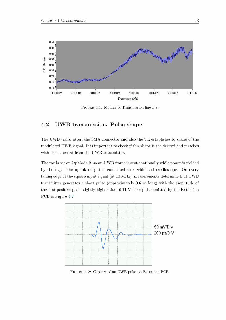
Chapter 4 Measurements 43
Figure 4.1: Module of Transmission line S11.
4.2 UWB transmission. Pulse shape
The UWB transmitter, the SMA connector and also the TL establishes to shape of the
modulated UWB signal. It is important to check if this shape is the desired and matches
with the expected from the UWB transmitter.
The tag is set on OpMode 2, so an UWB frame is sent continually while power is yielded
by the tag. The uplink output is connected to a wideband oscilloscope. On every
falling edge of the square input signal (at 10 MHz), measurements determine that UWB
transmitter generates a short pulse (approximately 0.6 ns long) with the amplitude of
the first positive peak slightly higher than 0.11 V. The pulse emitted by the Extension
PCB is Figure 4.2.
Figure 4.2: Capture of an UWB pulse on Extension PCB.
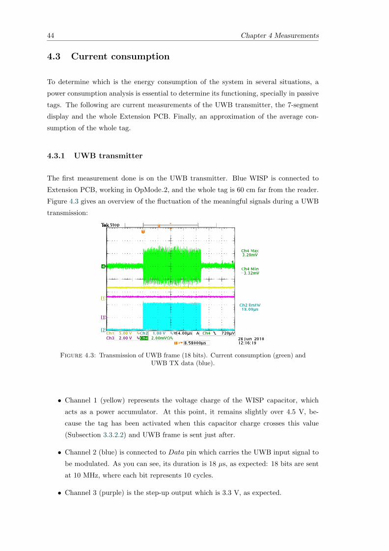
44 Chapter 4 Measurements
4.3 Current consumption
To determine which is the energy consumption of the system in several situations, a
power consumption analysis is essential to determine its functioning, specially in passive
tags. The following are current measurements of the UWB transmitter, the 7-segment
display and the whole Extension PCB. Finally, an approximation of the average con-
sumption of the whole tag.
4.3.1 UWB transmitter
The first measurement done is on the UWB transmitter. Blue WISP is connected to
Extension PCB, working in OpMode 2, and the whole tag is 60 cm far from the reader.
Figure 4.3 gives an overview of the fluctuation of the meaningful signals during a UWB
transmission:
Figure 4.3: Transmission of UWB frame (18 bits). Current consumption (green) andUWB TX data (blue).
• Channel 1 (yellow) represents the voltage charge of the WISP capacitor, which
acts as a power accumulator. At this point, it remains slightly over 4.5 V, be-
cause the tag has been activated when this capacitor charge crosses this value
(Subsection 3.3.2.2) and UWB frame is sent just after.
• Channel 2 (blue) is connected to Data pin which carries the UWB input signal to
be modulated. As you can see, its duration is 18 µs, as expected: 18 bits are sent
at 10 MHz, where each bit represents 10 cycles.
• Channel 3 (purple) is the step-up output which is 3.3 V, as expected.

Chapter 4 Measurements 45
• Channel 4 (green) represents the current consumption, measured at WISP V+
pin. Its shape is, like the UWB frame, a 18µs-long burst with maximum and
minimum peaks of 3.3 and -3.3 mA.
The bandwidth of the current probe is too low (DC-100 MHz) to measure the current
spikes produced by the UWB transmitter. These spikes are composed by different fre-
quencies that are higher than probe BW. Figure 4.4 shows the beginning of the UWB
burst and current fluctuation seems to be null in average because of current probe’s BW.
This is, obviously, false.
Figure 4.4: Transmission of UWB frame (zoom in). Current consumption (green)and UWB TX data (blue).
The following are captures of the same signals in the Extension PCB without a 7-segment
display, 150 cm away from the reader. So, a UWB frame is sent and display turned on
when 4.5 V are yielded, but display load is null (apart from small losses).
In Figure 4.5 the global fluctuation of the meaningful signals is shown. The capacitor
in WISP (yellow) is charging during 90 ms until it reaches 4.5 V. At this point, step-
up is switched on (purple) and raises its output up to 3.3 V, generating a current
consumption peak (green). Immediately after, an UWB frame is sent (blue). Then, tag
keeps supplying the PCB until its energy is consumed, 60 ms later, and the cycle begins
again.
Figure 4.6 zooms in the part where step-up is turned on. As can be seen in Channel
4 (green), this DC-DC converter generates high current peak (∼ 130 mA) followed by
3.4ms-periodic peaks (∼ 70 mA). The first one appears to raise up the output level from
2.4 to 3.3 V (in purple) and the following ones, to maintain the 3.3 V level, as described
in its data sheet.

46 Chapter 4 Measurements
Figure 4.5: Global functionality. Current consumption (green), capacitor voltage(yellow), step-up level (purple) and UWB TX data (blue).
Figure 4.6: Switching on the step-up. Current consumption (green), capacitor voltage(yellow), step-up level (purple) and UWB TX data (blue).
The UWB frame generates also a voltage burst, in step-up output, in Figure 4.7. Just
before, a 55µs-long group of increasing current peaks with a maximum of 130 mA can
be seen; this is the powering-up response of the step-up and it is also as expected in its
data sheet. Finally, one of the periodic peaks is captured in Figure 4.8; its maximum is
70 mA and is about 30 µs long.
4.3.2 7-segment display
The main load component in the Extension PCB is the display. It is a “common anode”
7-segment display, which means that the previous decoder sets a low output to turn on

Chapter 4 Measurements 47
Figure 4.7: Switching on the step-up (Zoom in). Current consumption (green), ca-pacitor voltage (yellow), step-up level (purple) and UWB TX data (blue).
Figure 4.8: Periodic current peak (green) generated by step-up.
any of its LEDs.
For this measurement, Blue WISP was reprogrammed to only toggle A1 and A0 pins
from ‘0’ to ‘1’ every 1.05 ms. In this way, display’s values are ‘4’ and BLANK. Moreover,
resistors R5 to R11 have been removed. Thus, the consumption of only one LED (‘F’
cathode, upper left) can be measured and Figure 4.9 describes this oscillation: Channel 2
(green) represents current consumed at “Current checkpoint” (battery is used). Channel
1 (yellow) draws the voltage level of the decoder output, from 0 to 1.8 V.
It is possible to see that, when decoder output is high, current level is null (LED off).
On the other hand, when decoder is low, current level is about 0.6 mA (LED on). This
is the expected value, because this LED (Agilent Technologies’ HDSP-7511) has a 1.8
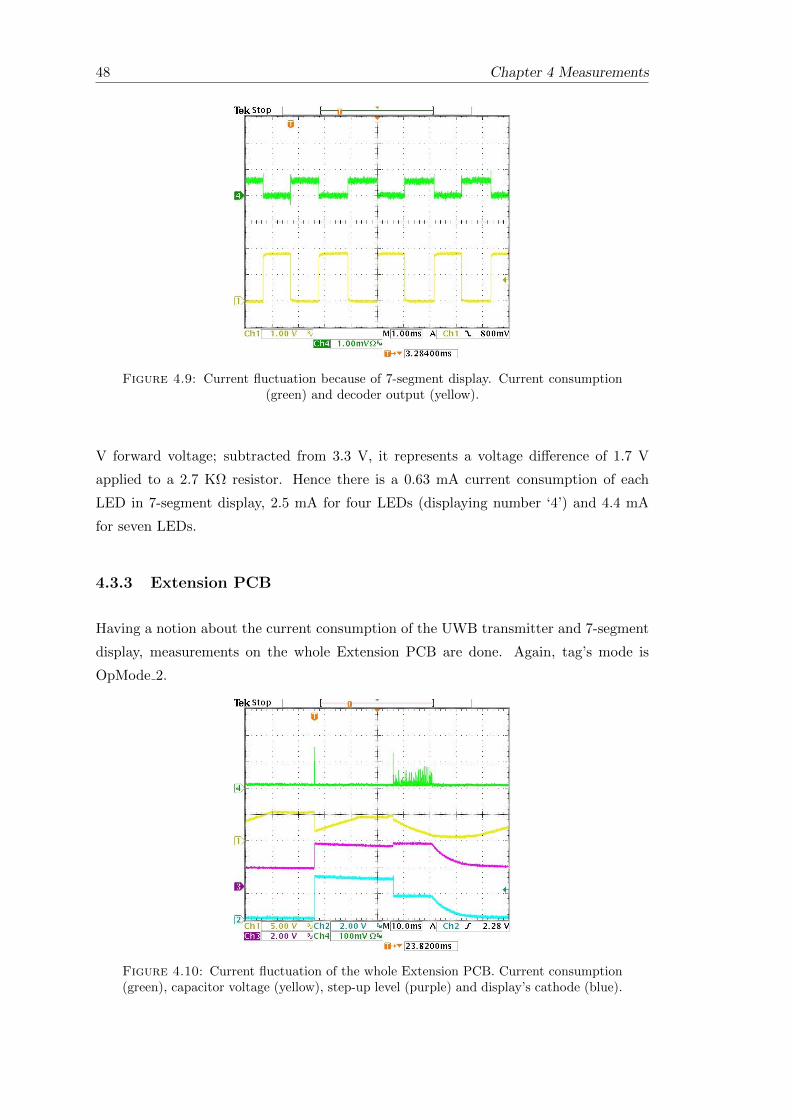
48 Chapter 4 Measurements
Figure 4.9: Current fluctuation because of 7-segment display. Current consumption(green) and decoder output (yellow).
V forward voltage; subtracted from 3.3 V, it represents a voltage difference of 1.7 V
applied to a 2.7 KΩ resistor. Hence there is a 0.63 mA current consumption of each
LED in 7-segment display, 2.5 mA for four LEDs (displaying number ‘4’) and 4.4 mA
for seven LEDs.
4.3.3 Extension PCB
Having a notion about the current consumption of the UWB transmitter and 7-segment
display, measurements on the whole Extension PCB are done. Again, tag’s mode is
OpMode 2.
Figure 4.10: Current fluctuation of the whole Extension PCB. Current consumption(green), capacitor voltage (yellow), step-up level (purple) and display’s cathode (blue).

Chapter 4 Measurements 49
Figure 4.10 shows the general functionality of the tag (Blue WISP + Extension PCB)
60 cm away from the reader. These are the important signals:
• Channel 1 (yellow) represents the voltage charge of the WISP capacitor. It raises
from 0 to 4.5 V, then tag is activated. At this moment, step-up raises up its output
to 3.3 V and it represents an important consumption. Tag sends an UWB frame
and turns on display 30 ms later, until energy is consumed.
• Channel 3 (purple) is the step-up output. When tag is activated, it maintains at
3.3 V, until energy stored at capacitor is consumed.
• Channel 2 (blue) is connected to one of display’s cathodes. Decoder starts at
3.3 V (high) and no voltage difference appears between resistor nodes; so, LED
is off and cathode at 3.3 V. 30 ms later, the decoder output is set to 0 V, LED
switches on and represents a 1.8 voltage difference; cathode is now at 1.7 V. When
capacitor (yellow) starts to run out, the same happens to step-up and, likewise, to
the cathode.
• Channel 4 (green) represents the current consumption, measured at WISP V+
pin. Two important peaks can be seen: the first (A), when step-up is switched on
and, the second (B), when display is activated. Afterwards, 220µs-periodic peaks
(C) appear to support display’s consumption.
Peak A in Figure 4.11 differs to from Figure 4.7 because of display load. Its maximum
is about 150 mA, but its duration is 220 µs. In addition, peak B’s maximum is 130 mA
and 65 µs long in Figure 4.12. Finally, each of the peaks (C) is exactly like Figure 4.8,
but period is shorter.
From the previous captures, an approximation of the average current consumption can
be achieved. This approximation depends on the energy of A, B and C peaks (IA, IB
and IC), on C-peaks periodicity (T ′), on the time when display is activated (TON ) and
on the global periodicity (T , time between successive tag’s ignitions). Equation C.2
gives this approximation in Subsection C.3.3.
This average depends only in TON and T , because IA, IB, IC and T ′ are constants. So,
defining the duty cycle (DC) as TON/T , the approximation of average consumption is in
Figure 4.13. T sweeps from 60 to 420 ms because these are the minimum and maximum
values measured on the Extension PCB (connected to a Blue WISP) with PCB display
(in Section 4.5).
It is possible to realise that, the higher the duty cycle and the periodicity are, the more
Iavg approaches to 2.27 mA. This value is the display’s consumption calculated from

50 Chapter 4 Measurements
Figure 4.11: First current peak (A), when step-up is switched on. Current consump-tion (green), capacitor voltage (yellow), step-up level (purple) and display’s cathode
(blue).
Figure 4.12: Second current peak (B), before display is switched on. Current con-sumption (green), capacitor voltage (yellow), step-up level (purple) and display’s cath-
ode (blue).
C peaks (Subsection C.3.3). In fact, this is the expected functionality: when DC and
periodicity are high, display is on most of the time, hence the average consumption
represents the display consumption.
In addition, using a multimeter, the average current consumption is around 1.5 mA at
60 cm away from the reader, using a battery. The periodicity at this point is 150 ms
and the duty cycle is 60 %, so 1.5 mA roughly matches with the approximation.

Chapter 4 Measurements 51
Figure 4.13: Average current consumption, Iavg (µA), as a function of DC (%) andT (ms).
4.4 Communication range
The following measurements are likewise important and describe the maximum distance
where the communication is still possible. In order to check the tag’s maximum range,
this measurement shows how far you can communicate Blue WISP to reader, working
in OpMode 1. Credipass application is used and issues a beep when a communication
between both is established; Extension PCB is not needed, in this case. The maximum
distance measured was two meters.
Figure 4.14: Laboratory distribution for measurements at different distances: oscil-loscope (red), Blue WISP + Extension PCB (green) + reader (blue).
Moreover, Extension PCB is connected to Blue WISP (in OpMode 2) and the power
voltage level (V out) in WISP is measured, Figure 4.14. Scavenging unit is able to
yield power up to, also, a little farther than two meters as well. Display active time,
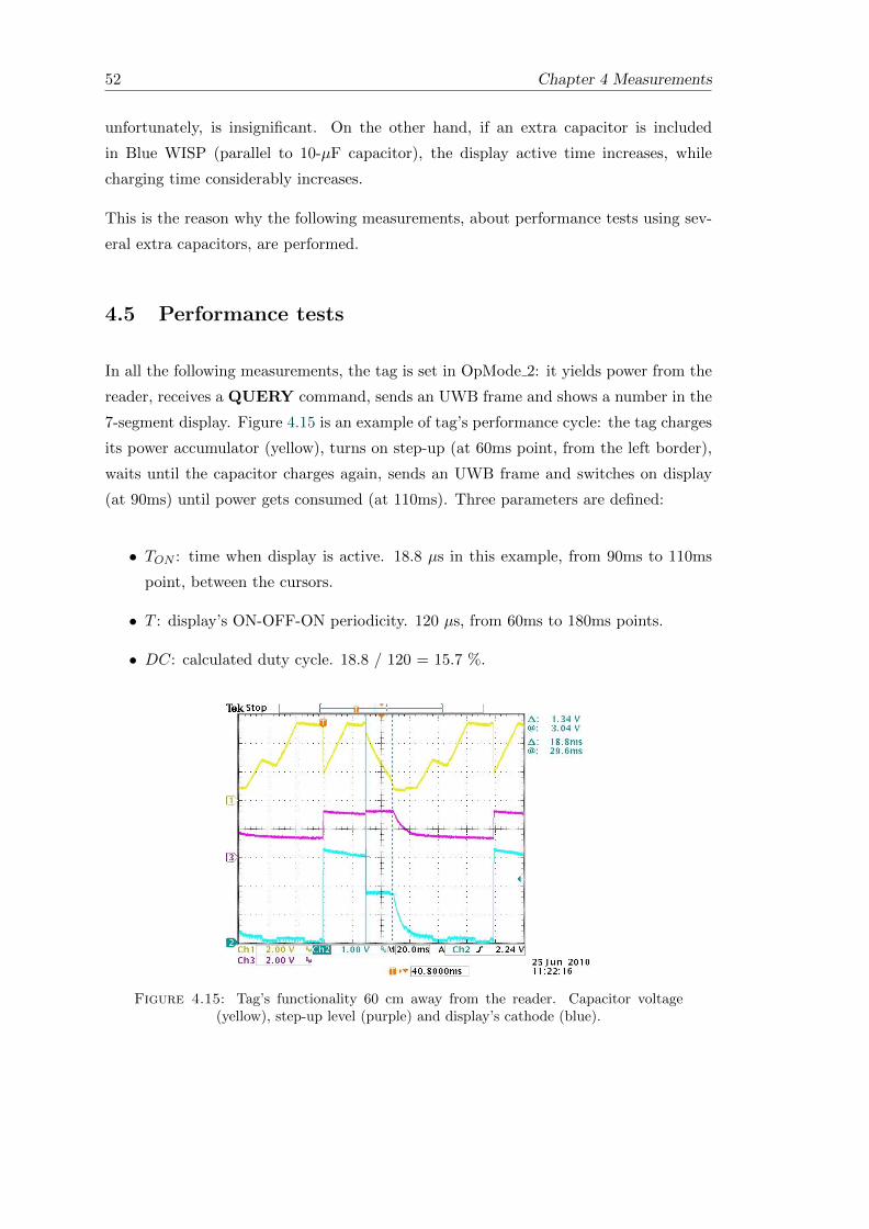
52 Chapter 4 Measurements
unfortunately, is insignificant. On the other hand, if an extra capacitor is included
in Blue WISP (parallel to 10-µF capacitor), the display active time increases, while
charging time considerably increases.
This is the reason why the following measurements, about performance tests using sev-
eral extra capacitors, are performed.
4.5 Performance tests
In all the following measurements, the tag is set in OpMode 2: it yields power from the
reader, receives a QUERY command, sends an UWB frame and shows a number in the
7-segment display. Figure 4.15 is an example of tag’s performance cycle: the tag charges
its power accumulator (yellow), turns on step-up (at 60ms point, from the left border),
waits until the capacitor charges again, sends an UWB frame and switches on display
(at 90ms) until power gets consumed (at 110ms). Three parameters are defined:
• TON : time when display is active. 18.8 µs in this example, from 90ms to 110ms
point, between the cursors.
• T : display’s ON-OFF-ON periodicity. 120 µs, from 60ms to 180ms points.
• DC: calculated duty cycle. 18.8 / 120 = 15.7 %.
Figure 4.15: Tag’s functionality 60 cm away from the reader. Capacitor voltage(yellow), step-up level (purple) and display’s cathode (blue).

Chapter 4 Measurements 53
4.5.1 “Ordinary” tag
Samples of those three parameters are obtained on the Extension PCB connected to a
“empty” Blue WISP (no extra capacitor). Table 4.3 summarizes those measurements,
where d is the distance to the reader (in cm), T is the period in ms, TON is display’s
active time in ms and DC is the duty cycle in %.
Please, note that T values have been fitted to 30 ms multiple. It is known that every
cycle starts when a Query command is sent by the reader and power is higher than 4.5
V, and the reader sends a Query every 30 ms. In this way, some accuracy errors are
avoided.
Table 4.3: Performance test of a “simple” Extension PCB.
d (cm) 25 60 100 150 200
TON (ms) 30.8 18.8 12 8 8T (ms) 90 120 210 420 420DC (%) 34.2 15.7 5.7 1.9 1.9
As is logical, the further the tag is, the harder it is to charge and the less is the active
time. Being near to the reader (25 cm), display is on for 34 % of the time and for 2 %,
being far (2 m).
4.5.2 “Battery-equipped” tag
Again, an Extension PCB with 7-segments display is checked, but 1.8 V battery (power
supply) is included.
Table 4.4: Performance test of a “battery-equipped” Extension PCB.
d (cm) 25 60 100 150 200
TON (ms) ∞ ∞ 90.4 60 60T (ms) - - 150 180 210DC (%) 100 100 60.3 33.3 28.6
It is possible to see that duty cycle in Table 4.4 increases in comparison to Table 4.3.
Display remains active continuously up to 60 cm and remains over 28 % up to 2 meters
away from the reader. This improvement happens, obviously, because of the battery;
tag’s loading is lighter due to the energy yielded, and is only used to keep the µC on,
listen to reader and administer the PCB.

54 Chapter 4 Measurements
4.5.3 “No-display” tag
WISP power yielded, step-up output and 1.8 V LDO (in the Extension PCB) were
inspected, using an Extension PCB without 7-segment display.
1.8 V LDO is always active. Figure 4.16 shows that power yielded (yellow) oscillates
from 1.4 V to 4.5 V. Step-up (purple) remains on (at 3.3 V) for 60 ms and off (decreasing)
for 90 ms. Even so, LDO (blue) is always on because step-up’s output is still higher
than 2 V.
Figure 4.16: Tag’s functionality 1.5 meters away from the reader, without display.Capacitor voltage (yellow), step-up level (purple) and display’s cathode (blue).
Moreover, it is important to pay attention to the power yielded shape (yellow curve):
steps appear in both growing and decreasing slopes. These steps are caused by the
reader; it sends a Query command every 30 ms, but it also sends a 20ms-long uniform
wave to charge the tag. Each of these 10ms-long step is the time when reader is sending
nothing, so tag is not charging (flat) on growing slope or discharging faster on decreasing
slope.
4.5.4 “Battery-equipped no-display” tag
The same happens when a battery is included; 1.8 V LDO is always active. The only
difference appears during the active time (discharging slope), which is longer in this
case, as expected. It is possible to see in Figure 4.17 that the step-up (purple) stays on
for about 90 ms, instead of 60 ms without battery in Figure 4.16.
Again, improvement appears thanks to the battery; the power yielded by Blue WISP
is only used to keep the µC on, listen to reader and administer Extension PCB. These
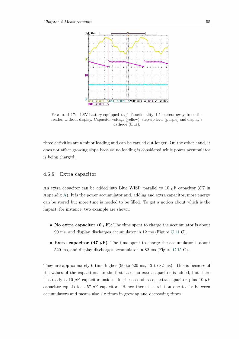
Chapter 4 Measurements 55
Figure 4.17: 1.8V-battery-equipped tag’s functionality 1.5 meters away from thereader, without display. Capacitor voltage (yellow), step-up level (purple) and display’s
cathode (blue).
three activities are a minor loading and can be carried out longer. On the other hand, it
does not affect growing slope because no loading is considered while power accumulator
is being charged.
4.5.5 Extra capacitor
An extra capacitor can be added into Blue WISP, parallel to 10 µF capacitor (C7 in
Appendix A). It is the power accumulator and, adding and extra capacitor, more energy
can be stored but more time is needed to be filled. To get a notion about which is the
impact, for instance, two example are shown:
• No extra capacitor (0 µF): The time spent to charge the accumulator is about
90 ms, and display discharges accumulator in 12 ms (Figure C.11 C).
• Extra capacitor (47 µF): The time spent to charge the accumulator is about
520 ms, and display discharges accumulator in 82 ms (Figure C.15 C).
They are approximately 6 time higher (90 to 520 ms, 12 to 82 ms). This is because of
the values of the capacitors. In the first case, no extra capacitor is added, but there
is already a 10-µF capacitor inside. In the second case, extra capacitor plus 10-µF
capacitor equals to a 57-µF capacitor. Hence there is a relation one to six between
accumulators and means also six times in growing and decreasing times.

56 Chapter 4 Measurements
Table 4.5 is a compilation of all the measurements done using several extra capacitors
(none, 47, 100, 470, 1000 and 4700 µF) and different distances (25, 60, 100, 150 and 200
cm) from the reader.
Table 4.5: Performance test of a Extension PCB with extra capacitor.
d (cm)25 60 100 150 200
0 µFTON (ms) 30.8 18.8 12 8 8T (ms) 90 120 210 420 420DC (%) 34.2 15.7 5.7 1.9 1.9
47 µFTON (ms) 1320 110 82 72 72T (ms) 1440 420 690 1560 1440DC (%) 91.7 26.2 11.9 4.6 5
100 µFTON (ms) 1590 230 176 152 144T (ms) 1770 750 1380 2850 2730DC (%) 89.8 30.7 12.8 5.3 5.3
4700 µFTON (ms) 3380 784 620 600 600T (ms) 3990 2700 6900 9780 11700DC (%) 84.7 29.0 9.0 6.1 5.1
1000 µFTON (ms) 7160 1740 1280 1360 1280T (ms) 8600 5510 12840 17640 18720DC (%) 83.3 31.6 10.0 7.7 6.8
4700 µFTON (ms) 45400 8560 6600 6000 6000T (ms) 48990 23310 37890 80940 65940DC (%) 92.7 36.7 17.4 7.4 9.1
Extracted from Table 4.5, Figure 4.18 shows the evolution of duty cycles. Apart from
0-µF curve, DC values keep approximately constant in each distance for any extra ca-
pacitor, which means that the charging time keeps a fixed proportion to the discharging
time for a certain distance. On the other hand, DC decreases (when distance increases)
because harvester obtains energy more slowly (the raising slope is longer) and the dis-
play’s load is the same at any distance (the discharging slope is equally fast).
Even so, 0-µF curve is substantially lower. The reason of this effect is the reader. It
sends a 30ms-periodic Query command that activates the tag; even in the case when
the accumulator is full before, the tag waits until another Query. It makes periodicity
longer and, so, DC lower. This effect is not appreciable in other cases, because raising
and decreasing times are considerably higher than 30 ms.
Table 4.6 shows the average DC. These values gives an idea of which is the effective
brightness of the display: 25 cm away from the reader, the display is active during the
88% of the time and only 6% when the tag is 2 meters away. Thus, a big extra capacitor
will be used only if long active times are required. On the contrary, a small capacitor
will be used if fast responses are needed.

Chapter 4 Measurements 57
Figure 4.18: Duty cycle, DC (%), evolution.
Table 4.6: Average DC. Measurements without extra capacitor are ignored.
d(cm) 25 60 100 150 200
DCavg (%) 88 31 12 6 6
4.6 Harvester’s charging time
Finally, harvester’s ability in WISP4.1 DL is measured. Figure 4.19 shows different
charging times, Tch (ms), as a function of distance and extra capacitor. They represent
the time passed since the power accumulator level is 1 V until it reaches 4.5 V. These
values have been extracted from Figures C.11, C.15, C.16, C.17, C.18 and C.19.
It can be seen that Tch stretches when distance or extra capacitor increase; this is the
expected functionality. Tch increases with the distance because the energy received by
the tag is lower when the tag is farther. Tch increases with the capacitor because more
energy is needed to fill a bigger capacitor; thus, more time is observed.
Note that Tch is longer than 70 seconds when a 4700-µF capacitor is added, and the tag
is farther than 100 cm. So, while designing, the value of the extra capacitor should be
chosen properly in order to accomplish the response time specifications.

58 Chapter 4 Measurements
Figure 4.19: Charging time, Tch (ms).
4.7 System specifications
Table 4.7 summarizes the results obtained in the measurements and gives the specifica-
tions of the system. Each measurement is described in the section (SECT.) spot.

Chapter 4 Measurements 59
Table 4.7: System specifications.
PARAMETER SYMB. CONDITIONS VALUE SECT.
Protocols developedEPC Global C1 G2
UWB RFID
RFID data rate (UL) RRFID ≤ 580 Kb/s1 2
UWB data rate (UL) RUWB ≤ 1.6 Mb/s1 3
Hardware included
7-segment display
Thermometer
Accelerometer
TL Reflection coefficient S11 In useful BW ≤ -12 dB 4.1
A current peak A1
“No-display” tag
130 mA
4.3C current peak C1 70 mA
C peaks’ period T ′1 3.4 ms
A current peak A2 150 mA
4.3B current peak B2 130 mA
C current peak C2 70 mA
C peaks’ period T ′2 220 µs
Display consumption Iavg Display ON4 2.27 mA 4.3
DL range d OpMode 1 and 2 2 m 4.4
Charging time Tch ≥ 7 ms5 4.6
1It depends on the maximum clock of the MSP430F2132 micro-controller (16 MHz [7]).2Maximum data rate is 16 MHz (maximum clock) divided by 2 (2-Miller encoding) and by 12 (because
of code implementation. See 3.3.1.2).3Maximum data rate is 16 MHz (maximum clock) divided by the minimum processing gain (10
b/symb).4The display is always showing the number four (‘4’).5The tag is 25 cm far and none extra capacitor is added.


Chapter 5
Conclusions
In this work, there is a description of the design of a programmable sensor node com-
patible with EPC Global C1 G2 that permits different data rates, coding schemes, and
backscattering or UWR-IR uplink. It is built above Intel WISP4.1 DL that implements
a power scavenging unit, UHF interface, and also controls the rest of the node (UWB
interface and 7-segment display) in the “Extension PCB”.
The first part of this work shows the background and motivation of this innovative
system. Afterwards, a description of the Intel WISP4.1 DL is given, explaining its
hardware as well as the software used to control it. The following part develops the
system implementation, while discussing how the “Extension PCB” is designed and
how the code is re-used and modified from the original. Since an UWB receiver is not
available, the programmed UWB RFID protocol cannot be tested. However, the EPC
Global C1 G2 works perfectly and the tag is able to stand the important load of a
7-segment display.
Next, there is a report of all the measurements made on the whole system: Intel WISP
connected to Extension PCB. Tag obtains power and RFID-communicates to the reader
up to two meters away from it. Moreover, Extension PCB current consumption presents
peaks up to 150 mA and, provided that display is always active, its average is 2.3 mA.
Obviously, the average current consumption depends on the application defined.
The following table compares the features achieved by the tag designed in this work to
Intel’s WISP4.1 DL and Berkeley’s Motes:
61

62 Chapter 5 Conclusions
Table 5.1: Comparison with Intel’s and Berkeley’s devices.
Berkeley’s Berkeley’s Intel’s UWB -
Mica 2 Telos WISP4.1 DL RFID tag
Micro-controller ATmega128 TI MSP430 TI MSP430 TI MSP430
UL/DL Band 1 GHz 2.4 GHz 900 MHz 3.1-4.8 / 0.9 GHz
UL/DL Modulation FSK O-QPKS ASK OOK / ASK
Data rate 38.4 Kb/s 250 Kb/s 64 Kb/s 1.6 Mb/s
Thermometer - -40 - 124 C -50 - 150 C -50 - 150 C
Humidity sensor - 0 - 100 %RH - -
Visible light sensor - 320 - 730 nm - -
Solar light sensor - 190 - 1100 nm - -
3D-accelerator - - - 10 000 g
7-segment display No No No Yes
Battery needed Yes Yes No No
Minimum supply 2.7 V 1.8 V 1.8 V 1.8 V
5.1 Future work
This considers considers some of the future steps in this project, in order to improve the
UWB RFID tag designed in this work.
Firstly, it is still essential to have an available reader to interact through UWB RFID
communication. Once the reader is ready, the operation mode OpMode 3 might be
tested.
Another important key is the dependence on Intel’s WISP4.1 DL. “Blue WISP” obtains
the power from the reader using a 5-stage bridge rectifier. It also includes sensors and the
micro-controller that administers the full tag. Hence the Intel’s WISP can be removed
and a thermometer, a humidity sensor, a 3D-accelerometer, a micro-controller and a
harvester unit might be added on the board. Moreover, the harvester ability might
be improved making it adjustable (to the the optimal amount of stages) and adding a
negative branch. This last issue would permit to obtain power from electromagnetic
field more than twice as faster: while one of the branches is supplying the node, the
other is charging.
The second of these improvements will be achieved replacing the 7-segments display by
a paper display. The goal of a display in this tag is to give visual information about
variables in the environment to users, but a 7-segments display is clearly an important

Chapter 5 Conclusions 63
load because of its high power consumption. Thus, the use of a paper display, which
load is notably lighter, would enlarge tag’s features.
The use of printed antennas might also allow this node to be a commercial one. Fur-
thermore, a RS-232 interface can be used to monitor any action taken by the tag, while
it is programming and tested.
There is a prototype proposal for a new UWB RFID node in Appendix D, where its
hardware is described.


Appendix A
Intel WISP4.1 DL. Schematic and
layout images
This appendix complements the Intel WISP4.1 DL description in Chapter 2. It contains
schematics and layout images of this device, obtained in “WISP wiki” [10].
A.1 Schematic
(First and second pages) Firstly, there is a general block diagram that shows the rela-
tionship between the three main parts of the device. The following three sheets are the
schematics themselves.
A.2 Layout images
(Third page) These are the back and front sides of the WISP4.1, antenna not included.
65

1
1
2
2
3
3
4
4
D D
C C
B B
A A
Title
Number RevisionSize
A
Date: 1/30/2009 Sheet ofFile: C:\local\..\WISP4.1DL_Top.SchDoc Drawn By:
Receive_RFIDReceive_RFID_Enable
Transmit_RFIDAntenna_Port_Signal
AFEWISP4.1DL_AFE.SchDoc
XLpwrXLx_analogXLy_analogXLz_analog
TempData_analogTemp_Pwr
LEDCtr1Vsense_analog
CapSense_IO
Vsense_enable
CapSenseLine
SensorsWISP4.1DL_Sensors.SchDoc
Receive_RFIDReceive_RFID_EnableTransmit_RFID
XLpwrXLx_analogXLy_analogXLz_analog
LEDCtr1Vsense_analog
Temp_PwrTempData_analog
CapSense_IO
Vsense_enable
CapSenseLine
Digital_1WISP4.1DL_Digital.SchDoc
P1 1
P2 2
SMA1
SMA Port
Copyright 2009 Intel Corp.Designers:
Daniel Yeager, Alanson Sample
PCB Layout Rules and Guidelines
5x5 Routing5mil clearance5mil trace width8mil trace width preferred
Via 8x12
Hole size 8mil annular ring 12mil
Prototron rules hole size plus 2mils of annular on either size (hole+4mil).More annular is needed for vias and probe points that will be man handled and repeatedly soldered and re-soldered
RF Signals(Above routing rules only valid for low frequency signals or digital I/O)
RF need larger vias and careful routing
Trace Thickness
1/2 oz. 0.7 mils1 oz. 1.4 mils2 oz. 2.8 mils
P0SMA101
P0SMA102
P0SMA101
P0SMA102
1
1
2
2
3
3
4
4
D D
C C
B B
A A
Title
Number RevisionSize
Letter
Date: 1/30/2009 Sheet ofFile: C:\local\..\WISP4.1DL_AFE.SchDoc Drawn By:
Control
Ant
Feed
er
Stage1
Stage2
Stage3
Stage4
Bitline
Vout
Bit Pwr
7pF
Cs1
7pF
Cs2
7pF
Cs3
7pF
Cs4
7pF
Cs5
10pFCp1
10uFC1
6.8nH
L1
12
EDESD5Z3.3T1
10pFCp2
10pFCp3
10pFCp4
1uFC2
D7RB751S40T1
2k
R3
1
3
2
D1HSMS-285C
1
3
2
D2HSMS-285C
1
3
2
D3HSMS-285C
1
3
2
D4HSMS-285C
1
3
2
D5HSMS-285C
5-20pF - Do Not StuffCV1
D6
RB751S40T1
TRANSMIT
RECEIVE3
52
14
+-
U1NCS2200SQ2T2G
3
1
2 Q2
NTK3134N
RECEIVE_ENABLE
VCCA1
Gnd3
A2 B 5
VCCB 6
OE 4
U2
NLSV1T244
Vreg
Receive_RFID
Receive_RFID_Enable
Transmit_RFID
Antenna_Port_Signal
PP1
compA
compFoot
Q1BFT25A
2
3
1
Q4BF1212WR
Copyright 2009 Intel Corp.Designers:
Daniel Yeager, Alanson Sample
P0C101
P0C102
P0C201
P0C202
P0Cp101
P0Cp102
P0Cp201
P0Cp202
P0Cp301
P0Cp302
P0Cp401
P0Cp402
P0Cs101 P0Cs102
P0Cs201 P0Cs202
P0Cs301 P0Cs302
P0Cs401 P0Cs402
P0Cs501 P0Cs502
P0CV101
P0CV102
P0D101
P0D102
P0D103
P0D201
P0D202
P0D203
P0D301
P0D302
P0D303
P0D401
P0D402
P0D403
P0D501
P0D502
P0D503
P0D601 P0D602
P0D701
P0D702
P0ED01
P0ED02
P0L101 P0L102
P0PP100
P0Q101
P0Q102
P0Q103
P0Q201
P0Q202 P0Q203
P0Q401
P0Q402
P0Q403
P0R301 P0R302
P0U101
P0U102
P0U103
P0U104
P0U105
P0U201
P0U202
P0U203 P0U204
P0U205
P0U206

1
1
2
2
3
3
4
4
5
5
6
6
D D
C C
B B
A A
Title
Number RevisionSize
Letter
Date: 1/30/2009 Sheet ofFile: C:\local\..\WISP4.1DL_Digital.SchDoc Drawn By:
TEST
RST
Transmit_RFID
GND
VregVreg
SCL1
Gnd2
SDA3
Vcc 4
WP 5
U7
24AA08
Vreg
XLx_analog
XLy_analog
XLz_analog
Vreg
10kR10
Vreg
10kR11
Cap
Sens
e_IO
1uFC20
DVss1
Xout/P2.72
Xin/P2.63
NC4
RST/SBW5
P2.0/A06
P2.1/A17
P2.2/A28
P3.0
/A5
9
P3.1
10
P3.2
11
P3.3
12
P3.4
13
P3.5
14
P3.6
/A6
15
P3.7
/A7
16
NC 17
P2.3/A3 18
P2.4/A4 19
NC 20
P1.0 21
P1.1 22
P1.2 23
P1.3 24
P1.4
25
P1.5
26
P1.6
27
P1.7
28
TEST
/SB
WC
lk29
Vcc
30
NC
31
P2.5
/Ros
c32
Vss0
MCU1MSP430x21x2
SCL_B
SDA_BSD
A_B
SCL_
B
Vse
nse_
anal
og
SCL_
B
Receive_RFID
Tem
pDat
a_an
alog
1
2
Y1
FC-135
LED
Ctr1
Receive_RFID_Enable
Supervisor
SMC
LK
CLK
_A
TX_S
IMO
_A
RX
_SO
MI_
A
XLp
wr
Temp_Pwr
CLK
_B
P36_
A6
P37_
A7
P23_A3
CLK
_A
SDA
_B
SDA
_BSC
L_B
CLK
_BTX
_SIM
O_A
RX
_SO
MI_
AP3
6_A
6P3
7_A
712345678
P3MHDR1X8
XOUT
XIN
SV_out
VDD 2
OUT 1VSS4
NC3
Threshold: 2.2v
U5
S1000C20-I4T1
SV_IN
VCCA1
Gnd3
A2 B 5
VCCB 6
OE 4
U4
NLSV1T244
Vreg
Vout
Supe
rvis
or
Vreg
Vout
1uFC14
CE1
GND2 Vout 3
Vin 4
Regulated Voltage: 1.8v
U3
NCP583
100R5
+
-
0.1F
C7MaxCap LX 0.1F
SCap
Cha
rge
Max
Cap
1k
R4
Supervisor
Vreg33k
R6
123
P4
MHDR1X3
4321
P1
MHDR1X4
RSTTEST
Vreg
GND
SV_INSMCLK
P23_A3
0
R1
Vse
nse_
enab
le
Cap
Sens
eLin
e
Rec
eive
_RFI
DR
ecei
ve_R
FID
_Ena
ble
VregSCapCharge
Vout
GND
P25
1 2 3 4 5 6 7 8
P2 MHDR1X8
P25
Copyright 2009 Intel Corp.Designers:
Daniel Yeager, Alanson Sample
Transmit:Must be connected to TAO (timer A output), usually P1.1
Receive:Code must be checked before this port can be changedMust be on a low value port number of port #1 (ie port 1.0, 1.2)This has to do with the constant generator in the MSP430 and its ability to quickly reference this port.
Supervisor Interrupt:Must be placed on port 2, so it does not collide with the read interrupt
P0C701
P0C702
P0C1401 P0C1402
P0C2001
P0C2002
P0MCU100
P0MCU101
P0MCU102
P0MCU103
P0MCU104
P0MCU105
P0MCU106
P0MCU107
P0MCU108
P0MCU109
P0MCU1010
P0MCU1011
P0MCU1012
P0MCU1013
P0MCU1014
P0MCU1015
P0MCU1016
P0MCU1017
P0MCU1018
P0MCU1019
P0MCU1020
P0MCU1021
P0MCU1022
P0MCU1023
P0MCU1024
P0MCU1025
P0MCU1026
P0MCU1027
P0MCU1028
P0MCU1029
P0MCU1030
P0MCU1031
P0MCU1032
P0P101
P0P102
P0P103
P0P104
P0P201
P0P202
P0P203
P0P204
P0P205
P0P206
P0P207
P0P208
P0P301
P0P302
P0P303
P0P304
P0P305
P0P306
P0P307
P0P308
P0P401
P0P402
P0P403
P0R101 P0R102
P0R401 P0R402
P0R501
P0R502
P0R601 P0R602
P0R1001
P0R1002
P0R1101
P0R1102
P0U301
P0U302 P0U303
P0U304
P0U401
P0U402
P0U403 P0U404
P0U405
P0U406
P0U501
P0U502 P0U503
P0U504
P0U701
P0U702
P0U703
P0U704
P0U705
P0Y101
P0Y102
1
1
2
2
3
3
4
4
D D
C C
B B
A A
Title
Number RevisionSize
A
Date: 1/30/2009 Sheet ofFile: C:\local\..\WISP4.1DL_Sensors.SchDoc Drawn By:
0.1uFC6
0.1uFC5
0.1uFC4
0.1uFC9
XLpwr
XLy
XLz
XLxNC1
ST2
COM3
NC4
CO
M5
CO
M6
CO
M7
Zout
8
NC 9
Yout 10
NC 11
Xout 12
NC
13
Vs
14
Vs
15
NC
16
NC 0
XLADXL330
100pFC12
0.1uFC13
Temp_PwrTemp_Data
GS1 5
Gnd2
Vcc 4
GS21
Out3
TMP
LM94021
3
1
2Q3NTK3134N
GND
LED_CTL_1
1k
R2
DA1
SML-311UTT86
66kR19
10pFC1033k
R17
Vout
Vsense
Vout
XLpwr
XLx_analog
XLy_analog
XLz_analog
TempData_analog Temp_Pwr
LEDCtr1
200kR16
10pFC111M
R18
CapSenseLine
CapSense_IOCapSense
led1 led2
3
1
2
Q5NTK3134N
NO1
COM2
GND3
Vcc 4
IN 5
U6
TS5A3166
Vout
Vse
nse_
anal
og
Vsense_enable
CapSenseLine
Copyright 2009 Intel Corp.Designers:
Daniel Yeager, Alanson Sample
P0C401
P0C402
P0C501
P0C502
P0C601
P0C602
P0C901
P0C902
P0C1001
P0C1002
P0C1101
P0C1102
P0C1201 P0C1202
P0C1301 P0C1302
P0DA101 P0DA102
P0Q301
P0Q302 P0Q303
P0Q501
P0Q502
P0Q503
P0R201 P0R202
P0R1601
P0R1602
P0R1701
P0R1702
P0R1801
P0R1802
P0R1901
P0R1902
P0TMP01
P0TMP02
P0TMP03 P0TMP04
P0TMP05
P0U601
P0U602
P0U603
P0U604
P0U605
P0XL00
P0XL01
P0XL02
P0XL03
P0XL04
P0XL05
P0XL06
P0XL07
P0XL08
P0XL09
P0XL010
P0XL011
P0XL012
P0XL013
P0XL014
P0XL015
P0XL016


Appendix B
Extension PCB. Schematic,
layout images and images
In order of appearance, this appendix contains: schematic, layout captures and images
of the “Extension PCB”. These sheets complement the description in Chapter 3.
B.1 Schematic
(First page) It is obtained by using OrCAD Capture 15.7. This schematic describes the
complete board, which is designed to be connected to Intel’s WISP4.1 DL. It is also used
to generate a MNL file to design the layout.
B.2 Layout images
(From second to fourth page) They are obtained by using OrCAD Layout 15.7. Parting
from that MNL file to initiate the layout design, all the component footprints are as-
signed, all the paths are routed, all the copper zones are defined and these four images
are generated. The first capture is the “assembly layer”, which contains the allocation
of all the components:
• ASSEMBLY layer. This layer is only used while designing in order to distribute
all the components among the PCB. It is only a descriptive layer, does not imple-
ment any material in the PCB.
The following four captures represent all the layers of the 4-layer PCB. In order of
appearance and from top to bottom in the PCB:
69

70 Appendix B Extension PCB. Schematic, layout images and images
• TOP layer. All the components are mounted on this layer. All the copper area
is linked to the GND node. On this layer are most of the paths.
• GND layer. The common GND node is on this layer.
• PWR layer. The 3.3 V node is on this layer. The squares on the corners avoid
a short-circuit between GND and PWR through the screws.
• BOTTOM. The remaining paths which can not be routed on TOP layer are on
BOTTOM layer. In the same way, the copper area is linked to the GND node.
The real size of the PCB (in mm) is 77.25 x 60,75. The PCB used is a four-layer PCB
(1.6 mm): 18 um copper on top and bottom layer, 0.36 mm isolation between top and
ground and between power and bottom layers, 35 um copper on ground and power layers
and 0.79 mm isolation between them.
B.3 Images
(Fifth page) There are two photographies of the Extension PCB. The first is an image
of an empty PCB (no components included/soldered). The other is a plan view of the
complete PCB.
Figure B.1: “Empty” WISP Extension PCB.

5
5
4
4
3
3
2
2
1
1
D D
C C
B B
A A
DataPSDCtrlAmpCtrl
WISP_V-
WISP_V+
PB_V+
A0
A1
PB_V-
Strobe
SHDN*
V1.8
V3.3
V1.8 V1.8
V1.8
V3.3V3.3
V3.3
V3.3
Title
Size Document Number Rev
Date: Sheet of
<Doc> <RevCode>
WISP4.1 DL extension PCB (UWB & 7segments)
A4
1 1Wednesday, September 22, 2010
Title
Size Document Number Rev
Date: Sheet of
<Doc> <RevCode>
WISP4.1 DL extension PCB (UWB & 7segments)
A4
1 1Wednesday, September 22, 2010
Title
Size Document Number Rev
Date: Sheet of
<Doc> <RevCode>
WISP4.1 DL extension PCB (UWB & 7segments)
A4
1 1Wednesday, September 22, 2010
PaperBattery
Choice of energy source
Current checkpoint
VCC
ExtIn
GND
freq. in
freq. in
Freq. input choice
Ext. in
U5
C41uFC41uF
R2xR2x
R131MR131M
u1
m2
d3
C210uFC210uF
R8 2.7kR8 2.7k
R112.7kR112.7k
C81uFC81uF
C71uFC7
1uF
C6100nFC6100nF
U9
2pins_254mm
U9
2pins_254mm
pin11
pin22
U3
HCF4056B
U3
HCF4056B
STROBE 11
BCD 2_22
BCD 2_13
BCD 2_34
BCD 2_05
freq. in6
Vee7
Vss8 a 9b 10c 11d 12e 13g 14f 15
Vdd 16
U8
2pins_254mm
U8
2pins_254mm
pin1 1pin2 2
R3100kR3100k
L1 47uHL1 47uH1 2
U11
6pins_254mm
U11
6pins_254mm
pin11
pin22
pin33
pin44
pin55
pin66
U6
8pinsMale_2
U6
8pinsMale_2
pin1 1pin2 2pin3 3pin4 4pin5 5pin6 6pin7 7pin8 8
R121MR121M
u1
m2
d3
R7 2.7kR7 2.7k
U13
SMAconnector
U13
SMAconnector
pin11
pin22
pin33
pin44
pin55
R6 2.7kR6 2.7k
U7
3pins_254mm
U7
3pins_254mm
pin1 1pin2 2pin3 3
U4
HDSP-7511
U4
HDSP-7511
anode1
cath F2
cath G3
cath E4
cath D5 anode 6cath DP 7
cath C 8cath B 9cath A 10
C91uFC91uF
R5 2.7kR5 2.7k
UWB transmitterUWB transmitter
.1
.2
.3
.4
.5
.6
.7
.8
.9
.10
.11
.12
.13
.14
.15
.16
.17
.18
.19
.20
.21
.22
.23
.24
. 36
. 35
. 34
. 33
TX Out 32
TX Out 31
. 30
. 29
. 28
. 27
. 26
. 25
.48
.47
.46
.45
.44
VC
C 1
.843
VC
C A
nalo
g42
Inpu
t41
PS
D C
trl
40
Am
pltu
de C
trl
39
VC
C D
igita
l38
.37
GND 49
R11MR11M
C31uFC31uF
R4 2.7kR4 2.7k
R10 2.7kR10 2.7k
U12
8pinsMale_1
U12
8pinsMale_1
pin1 1pin2 2pin3 3pin4 4pin5 5pin6 6pin7 7pin8 8
U10
3pinsMale
U10
3pinsMale
pin1 1pin2 2pin3 3
U1
MAX1678
U1
MAX1678
BATT1
PFI2
PFO3
SHDN*4
FB5 GND 6
LX 7
OUT 8
C5100nFC5100nF
C110uFC110uF
NCP583
U2
NCP583
U2
CE1
GND2 Vout 3Vin 4
R9 2.7kR9 2.7k

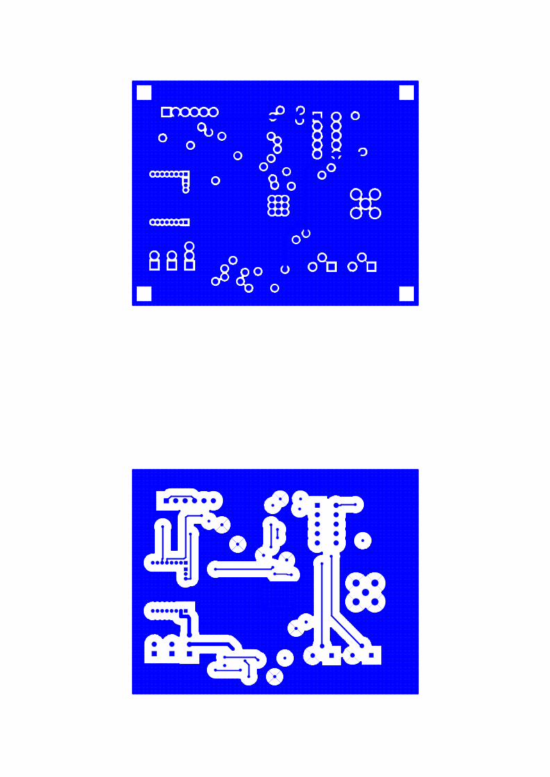
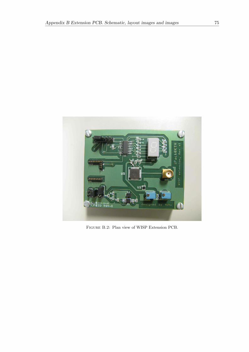
Appendix B Extension PCB. Schematic, layout images and images 75
Figure B.2: Plan view of WISP Extension PCB.


Appendix C
Measurements
This appendix contains the compilation of all the data obtained in the laboratory that
is not already published in Chapter 4. In this appendix, there is also a description of
the way these measurements are done.
In order of appearance, the measurements are: reflection coefficient of the transmission
line, shape of an UWB pulse, current consumption, communication range, performance
tests and harvester’s charging time.
C.1 Transmission line to uplink antenna. Reflection coef-
ficient (S11)
This parameter belongs to the transmission line between the output of the UWB trans-
mitter and the SMA connector that sends the signal through the uplink antenna. It
gives an idea about which is the energy loss because of impedance matching between
them.
To measure this parameter, a signal into one port of a TL is injected, add an adapted
resistor on the other port and analyse the reflected signal on the first port. Basically,
the vectorial analyser sweeps the whole bandwidth desired and keeps the value of the
reflection level on each frequency. The module of S11 is relative, so it is always between
0 and 1.
This measurement is described in Figure C.1. Using an empty Extension PCB, a SMA
connector is soldered where the uplink antenna may be allocated and a 50 Ω resistor is
soldered on the other port, between TL and the GND node, where the UWB transmitter
77

78 Appendix C Measurements
will be allocated. Vectorial analyser is connected to the PCB through the SMA connector
and measurement was done.
Figure C.1: Schematic of the S11 measurement.
The capture get from this measurement is Figure 4.1.
C.2 UWB transmission. Pulse shape
It is also important to check if the shape of the emitted UWB frame is as expected.
The output UWB-modulated signal can be deformed because of the TL design and the
impedance matching between the UWB transmitter, the TL and the SMA connector.
The way to compare this signal to the desired one is by getting a capture of the sent
UWB frame (or one of its pulses) and make a comparison of its characteristics. So, the
Blue WISP is connected to the Extension PCB and set the tag in OpMode 2; it will send
a UWB frame continually, while power is yielded by the tag. Since the UWB-modulated
signal is a high-frequency signal, a wideband oscilloscope is required. Figure C.2 shows
the system connection.
Figure C.2: Schematic of the pulse shape measurement.
The capture get from this measurement is Figure 4.2.

Appendix C Measurements 79
C.3 Current consumption
To get data on tag’s consumption, its current fluctuation is measured using Tektronix’s
TCP312 current probe and Tektronix’s TCPA300 amplifier [8] [9].
C.3.1 UWB transmitter
To measure UWB transmitter consumption, as can be seen in Figure C.3, Blue WISP’s
accumulator (yellow) is connected to oscilloscope’s Channel 1, UWB transmitter’s out-
put (blue) to Channel 2, step-up’s output (purple) to channel 3 and current probe at
UWB transmitter’s power node to channel 4 (green). In this case, 7-segments display is
not soldered on Extension PCB, which is working in OpMode 2 60 cm away from the
reader.
Figure C.3: Schematic of the current measurement of the UWB transmitter.
Captures that are not included in Chapter 4 are:
• Figure C.4 A: global view of step-up raising and UWB frame sending.
• Figure C.4 B: beginning of the burst.
• Figure C.4 C: middle part of the burst.
• Figure C.4 D: entire UWB frame.
• Figure C.4 E: beginning of the burst. Zoom in.
• Figure C.4 F: middle part of the burst. Zoom in.
As said in Subsection 4.3.1, measurements about current when UWB frame is sent can
be ignored because of current probe bandwidth.

80 Appendix C Measurements
Figure C.4: Captures of UWB transmitter’s current consumption. Figures on top:A, B, C; bottom: D, E, F.
Other captures about the Extension PCB’s global functionality (without 7-segment dis-
play) that are not included in Chapter 4 are:
• Figure C.5 A: global functionality.
• Figure C.5 B: global functionality. Zoom in.
• Figure C.5 C: periodical peaks.
• Figure C.5 D: UWB and step-up’s burst.
• Figure C.5 E: UWB and step-up’s burst. Zoom in.
C.3.2 7-segment display
To measure 7-segment display consumption, an Extension PCB with only 7-segment
display and its decoder is used. A 3.3 V battery is linked to V 3.3 node. Blue WISP is
reprogrammed to only toggle A1 and A0 pins from ‘0’ to ‘1’ every 1.05 ms. Channel
1 (yellow) is connected to decoder’s output (before resistor at display) and Channel 4
(green) to battery anode (Figure C.6).
Captures that are not included in Chapter 4 are:
• Figure C.7 A: ON-OFF display’s edge and decoder’s delay.

Appendix C Measurements 81
Figure C.5: Captures of Extension PCB (without display) current consumption. Fig-ures on top: A, B, C; bottom: D, E.
Figure C.6: Schematic of the current measurement of the 7-segment display.
• Figure C.7 B: OFF-ON display’s edge and decoder’s delay.
• Figure C.7 C: ON-OFF display’s edge. Zoom out.
• Figure C.7 D: OFF-ON display’s edge. Zoom out.
Note that only one segment on display was switching on, as said in Subsection 4.3.2.
C.3.3 Extension PCB
Again, Extension PCB in OpMode 2 is connected to Blue WISP, 150 cm away from
the reader. The connection diagram is Figure C.8: accumulator connected to Channel

82 Appendix C Measurements
Figure C.7: Captures of display’s current consumption. Figures on top: A, B; bottom:C, D.
1, display’s cathode to Channel 2, step-up’s output to Channel 3 and current probe at
WISP V+ pin to Channel 4.
Figure C.8: Schematic of the current measurement of the global battery consumption.
Captures that are not included in Chapter 4 are:
• Figure C.9 A: global functionality.
• Figure C.9 B: display’s lighting.
• Figure C.9 C: display’s lighting. Zoom in.
• Figure C.9 D: display’s lighting. Zoom in. Channel 3 (purple) shows the output
of UWB transmitter.

Appendix C Measurements 83
• Figure C.9 E: periodical peaks due to display.
• Figure C.9 F: periodical peaks due to display. Zoom in.
Figure C.9: Captures of Extension PCB current consumption. Figures on top: A, B,C; bottom: D, E, F.
Moreover, since peaks A, B, C and C-peaks periodicity are constant, an approximation
of average current consumption can be obtained using with the following equation:
Iavg =IA + IB +
ICT ′· TON
T(C.1)
where IA is the area of peak A (in A·s) in Figure 4.11, IB is the area of peak B (in A·s)in Figure 4.12, IC is the area of peak C (in A·s) in Figure 4.8, T ′ is the fixed periodicity
(220 µs) of peaks C when display in on, TON is the absolute time when display is on
and T is the global periodicity.
This equation is the addition of all the current peaks absorbed by the step-up. IA, IB
and IC are absolute vales and TON/T′ is equivalent to the number of times that C-peak
appears. IA, IB and IC are, actually, energy values (current · time), but the average
current is obtained dividing the energy consumed in a certain time by this certain time.
IA can be calculated as a trapezoid plus two rectangles: 50-to-120-mA high and 30-µs
long, 120-mA and 90-µs long, 70-mA high and 100-µs long, respectively; it is 20350
mA·µs. IB can be calculated as two trapezoids: 40-to-90-mA high and 40-µs long, 90-
to-60-mA high and 40-µs long; it is 5600 mA·µs. IC can be calculated as two triangles:
70-mA high and 8-µs long, 20-mA high and 22-µs long; it is 500 mA·µs. Which means:
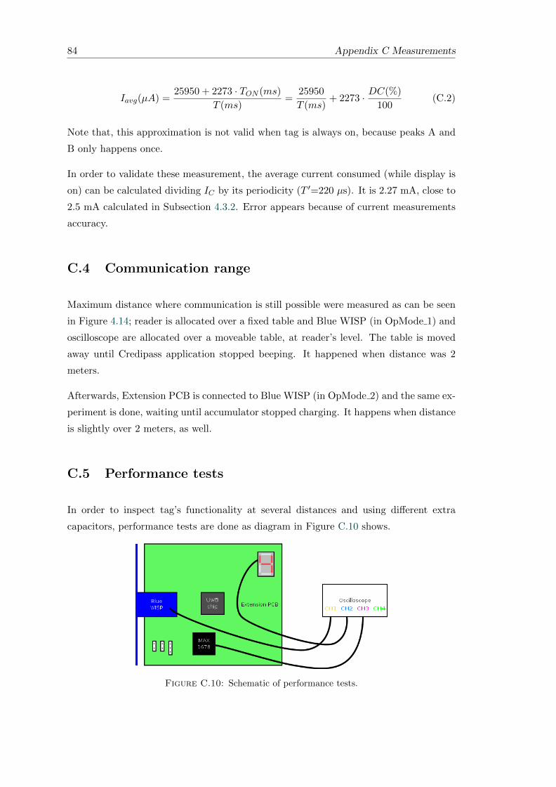
84 Appendix C Measurements
Iavg(µA) =25950 + 2273 · TON (ms)
T (ms)=
25950
T (ms)+ 2273 · DC(%)
100(C.2)
Note that, this approximation is not valid when tag is always on, because peaks A and
B only happens once.
In order to validate these measurement, the average current consumed (while display is
on) can be calculated dividing IC by its periodicity (T ′=220 µs). It is 2.27 mA, close to
2.5 mA calculated in Subsection 4.3.2. Error appears because of current measurements
accuracy.
C.4 Communication range
Maximum distance where communication is still possible were measured as can be seen
in Figure 4.14; reader is allocated over a fixed table and Blue WISP (in OpMode 1) and
oscilloscope are allocated over a moveable table, at reader’s level. The table is moved
away until Credipass application stopped beeping. It happened when distance was 2
meters.
Afterwards, Extension PCB is connected to Blue WISP (in OpMode 2) and the same ex-
periment is done, waiting until accumulator stopped charging. It happens when distance
is slightly over 2 meters, as well.
C.5 Performance tests
In order to inspect tag’s functionality at several distances and using different extra
capacitors, performance tests are done as diagram in Figure C.10 shows.
Figure C.10: Schematic of performance tests.

Appendix C Measurements 85
C.5.1 “Ordinary” tag
Figure C.11 A, B, C, D and E represent Extension PCB performance at 25, 60, 100, 150
and 200 cm from the reader, respectively.
Figure C.11: Captures of Extension PCB performance for several distances. Figureson top: A, B, C; bottom: D, E.
C.5.2 “Battery-equipped” tag
Figure C.12 A, B, C, D and E represent Extension PCB performance at 25, 60, 100, 150
and 200 cm from the reader, respectively, when no display is soldered on it.
C.5.3 “No-display” tag
Figure C.13 A, B, C, D and E represent Extension PCB performance at 25, 60, 100, 150
and 200 cm from the reader, respectively, when a battery is connected.
C.5.4 “Battery-equipped no-display” tag
Figure C.14 A, B, C, D and E represent Extension PCB performance at 25, 60, 100,
150 and 200 cm from the reader, respectively, when no display is soldered on it and a
battery is connected.
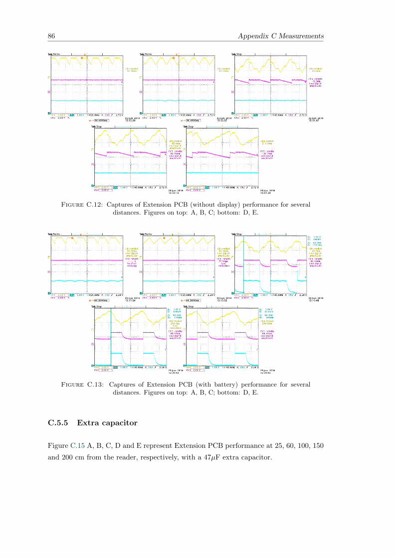
86 Appendix C Measurements
Figure C.12: Captures of Extension PCB (without display) performance for severaldistances. Figures on top: A, B, C; bottom: D, E.
Figure C.13: Captures of Extension PCB (with battery) performance for severaldistances. Figures on top: A, B, C; bottom: D, E.
C.5.5 Extra capacitor
Figure C.15 A, B, C, D and E represent Extension PCB performance at 25, 60, 100, 150
and 200 cm from the reader, respectively, with a 47µF extra capacitor.
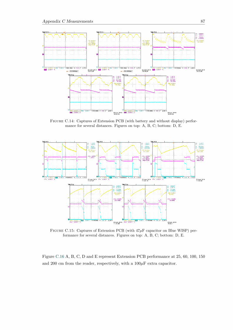
Appendix C Measurements 87
Figure C.14: Captures of Extension PCB (with battery and without display) perfor-mance for several distances. Figures on top: A, B, C; bottom: D, E.
Figure C.15: Captures of Extension PCB (with 47µF capacitor on Blue WISP) per-formance for several distances. Figures on top: A, B, C; bottom: D, E.
Figure C.16 A, B, C, D and E represent Extension PCB performance at 25, 60, 100, 150
and 200 cm from the reader, respectively, with a 100µF extra capacitor.

88 Appendix C Measurements
Figure C.16: Captures of Extension PCB (with 100µF capacitor on Blue WISP)performance for several distances. Figures on top: A, B, C; bottom: D, E.
Figure C.17 A, B, C, D and E represent Extension PCB performance at 25, 60, 100, 150
and 200 cm from the reader, respectively, with a 470µF extra capacitor.
Figure C.17: Captures of Extension PCB (with 470µF capacitor on Blue WISP)performance for several distances. Figures on top: A, B, C; bottom: D, E.
Figure C.18 A, B, C, D and E represent Extension PCB performance at 25, 60, 100, 150
and 200 cm from the reader, respectively, with a 1000µF extra capacitor.
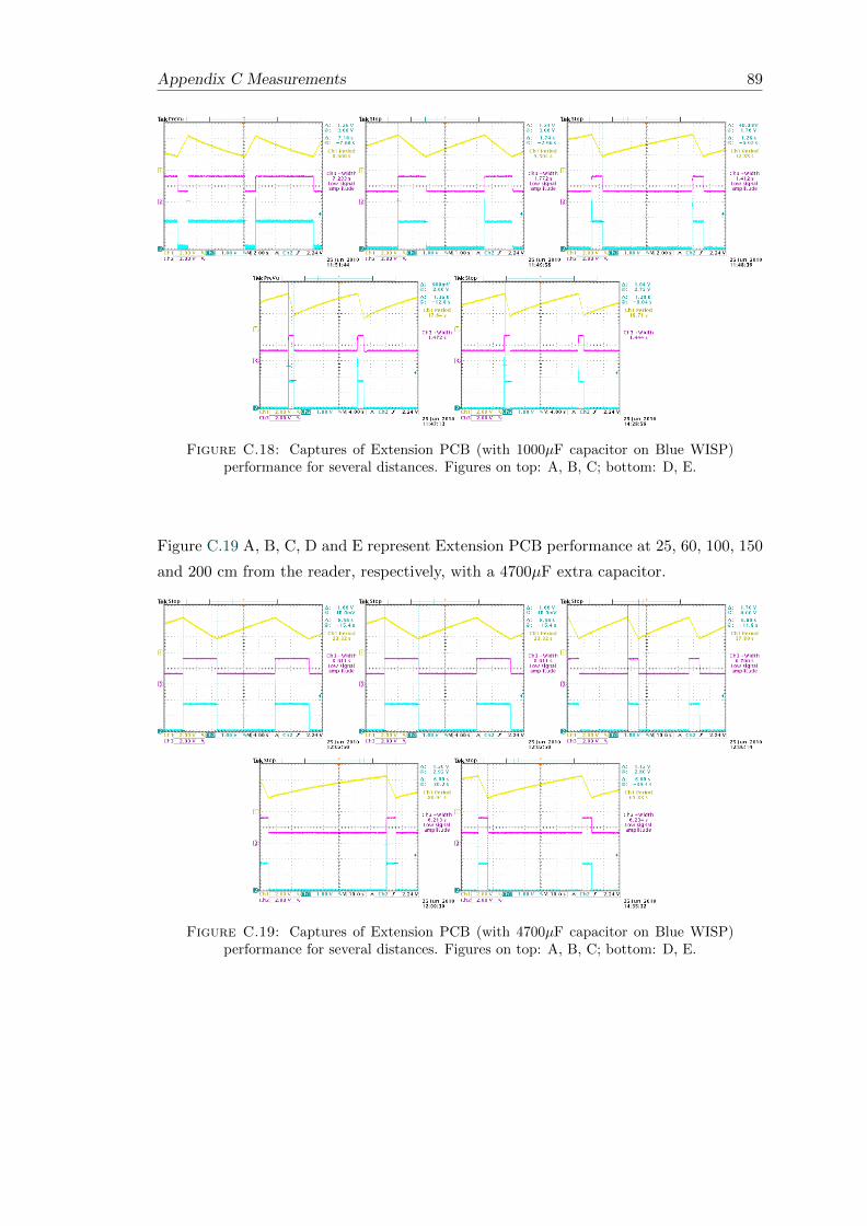
Appendix C Measurements 89
Figure C.18: Captures of Extension PCB (with 1000µF capacitor on Blue WISP)performance for several distances. Figures on top: A, B, C; bottom: D, E.
Figure C.19 A, B, C, D and E represent Extension PCB performance at 25, 60, 100, 150
and 200 cm from the reader, respectively, with a 4700µF extra capacitor.
Figure C.19: Captures of Extension PCB (with 4700µF capacitor on Blue WISP)performance for several distances. Figures on top: A, B, C; bottom: D, E.

90 Appendix C Measurements
C.6 Harvester’s charging time
Finally, to check how powerful the harvester in Intel WISP4.1 DL is, a calculation of the
time it spends to charge the power accumulator (capacitor) is done. This measurements
depend, of course, on the distance between the reader and the tag and depend also on
which is the extra capacitor added to increase the energy stored.
Taking advantage of the captures in the endurance tests (Sections 4.5 and C.5), the
time passed while capacitor is charging is measured. In fact, these measurements on
the captures are taken from the point where the capacitor’s level is 1.6 V until it is 4.4
V. These levels are chosen because they are easy to frame in the captures obtained and
both appear in all the charging slopes for all the cases. Afterwards, an extension factor
is applied to get the charging time as if the voltage level raises from 1 to 4.5 V.
As an example, Figure C.20 explains how these times are obtained. The red square
represents the voltage level limits (1.6 and 4.4 V) and the time limits (-220 and 200 ms);
so, 200 - (-220) ms = 420 ms is the charging time. The orange square represents the full
charging slope, from 1 to 4.5 V. It can be seen that the real charging time is 520 ms.
Since all the curves inspected present the same shape, the extension factor (520/420 =
1.24) is applied to all the measurements.
Figure C.20: Capture of Extension PCB (with 47µF capacitor on Blue WISP) per-formance 100 cm far from the reader. It is an expanded version of Figure C.15 C.
Table C.1 is the extract of the values obtained.

Appendix C Measurements 91
Table C.1: Charging time, Tch (ms), of Intel WISP harvester.
CHARGING TIME, Tch (ms)
d (cm) 25 60 100 150 200
0 µF 7 35 79 173 161
47 µF 74 235 520 1337 1188
100 µF 198 482 1139 2575 2525
470 µF 742 2278 7800 11142 12123
1000 µF 1733 4209 14114 18819 19314
4700 µF 4952 18323 38380 92857 74285

Appendix D
Hardware description of the
WISP prototype proposal
This appendix contains a description of the hardware designed for a WISP prototype
proposal. This prototype is designed to be a WISP with a high-efficiency power supply
stage and a UWB uplink. It includes a downlink and an uplink antennas, a power supply
stage (with a paper battery), a demodulator, an humidity and temperature sensor, an
accelerometer, a micro-controller, a UWB transmitter and a RS-232 interface. It has
been designed to be adjustable and thus find the optimal design of power harvesting
stage.
In order to divide all the components, the prototype is defined in three different blocks
(see Figure D.1):
• Power supply and Demodulator. This part processes the incoming power and
demodulates the reader’s request (downlink).
• Micro-controller, UWB transmitter and RS-232 interface. It controls all
the system, communicates to the reader (uplink) and sends every event through
RS-232.
• Sensors. It includes the humidity and temperature sensors and the accelerometer.
At the end, there are the detailed schematics of these parts of the hardware.
93
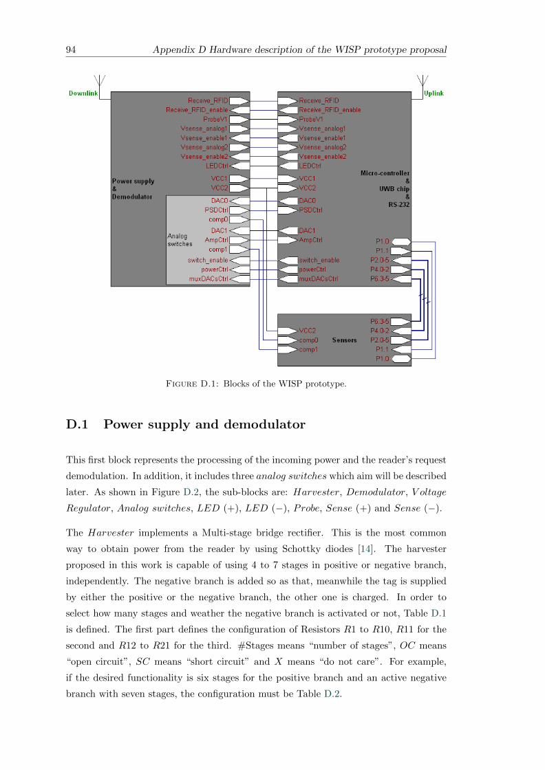
94 Appendix D Hardware description of the WISP prototype proposal
Figure D.1: Blocks of the WISP prototype.
D.1 Power supply and demodulator
This first block represents the processing of the incoming power and the reader’s request
demodulation. In addition, it includes three analog switches which aim will be described
later. As shown in Figure D.2, the sub-blocks are: Harvester, Demodulator, V oltage
Regulator, Analog switches, LED (+), LED (−), Probe, Sense (+) and Sense (−).
The Harvester implements a Multi-stage bridge rectifier. This is the most common
way to obtain power from the reader by using Schottky diodes [14]. The harvester
proposed in this work is capable of using 4 to 7 stages in positive or negative branch,
independently. The negative branch is added so as that, meanwhile the tag is supplied
by either the positive or the negative branch, the other one is charged. In order to
select how many stages and weather the negative branch is activated or not, Table D.1
is defined. The first part defines the configuration of Resistors R1 to R10, R11 for the
second and R12 to R21 for the third. #Stages means “number of stages”, OC means
“open circuit”, SC means “short circuit” and X means “do not care”. For example,
if the desired functionality is six stages for the positive branch and an active negative
branch with seven stages, the configuration must be Table D.2.

Appendix D Hardware description of the WISP prototype proposal 95
Figure D.2: Sub-blocks in the power supply and demodulator block.
Table D.1: Configuration of the resistors R1 to R21 to adjust Harvester’s functional-ity.
#Stages R1 R2 R3 R4 R5 R6 R7 R8 R9 R10
4 OC X X SC OC X X X X OC5 SC OC X OC SC SC OC X X OC6 SC SC OC OC SC OC SC SC OC OC7 SC SC SC OC SC OC SC OC SC SC
Negative Branch R11
OFF OCON SC
#Stages R12 R13 R14 R15 R16 R17 R18 R19 R20 R21
4 OC X X SC OC X X X X OC5 SC OC X OC SC SC OC X X OC6 SC SC OC OC SC OC SC SC OC OC7 SC SC SC OC SC OC SC OC SC SC
Moreover, the Harvester ends with two big capacitors (C11 and C12) which act as
power supplies. Note that C11 will hold a positive voltage, in V 1, whereas C12 will
hold a negative voltage, in V 2. Into the bargain, the Demodulator is linked to the final
stage of the Harvester’s positive branch.
The Demodulator has a voltage comparator which demodulates the input signal. Subse-
quently, a level translator (On semiconductor’s NLSV1T244) level-adapts the demodu-
lated signal in order to be sent properly to the micro-controller, through Receive RFID

96 Appendix D Hardware description of the WISP prototype proposal
Table D.2: Example of configuration of the resistors R1 to R21.
R1 SC R8 SC R15 OCR2 SC R9 OC R16 SCR3 OC R10 OC R17 OCR4 OC R11 SC R18 SCR5 SC R12 SC R19 OCR6 OC R13 SC R20 SCR7 SC R14 SC R21 SC
pin. Additionally, to save energy, Receive RFID enable pin is set to disable de demod-
ulator when input signal is not received.
In order to supply all the components, the V oltage Regulator provides 1.8 V and 3.3 V
from V 1 and V 2. In one hand, the positive Harvester’s output, V 1, is stabilized using
a 1.8 V Low drop-out regulator (LDO). To reach this target, an On semiconductor’s
NCP583 is chosen. Consequently, 1.8 V are in V 1′. On the other hand, a switched-
capacitor voltage inverter (Maxim’s MAX828, U6) is used to obtain a positive voltage
from V 2 to V 2′. In the same way that has been seen previously, a LDO yields 1.8 V
in V 2′′. At this point, V 1′ and V 2′′ hold 1.8 V. One of the Analog switches is used
to select which power supply to use, controlled by powerCtrl pin. Thus, the switch’s
output is the supply for all the components which need 1.8 V. This node is tagged as
V CC1.
There are two other Analog switches in Analog Devices’s ADG733. Their aim will be
explained in Subsections D.2 and D.3.
Furthermore, a 3.3 V power supply is needed. In this case, only the positive branch is
used to feed a step-up DC-DC converter (Maxim’s MAX1606). It raises up its voltage
input to 3.3 V in V CC2 node, but no LDO regulator is added afterwards because no
one of the components (feet with 3.3 V) needs an accurate an stable voltage supply;
some fluctuations do not affect on its functionality. Additionally, a paper battery can
included in order to obtain extra energy, if necessary.
LEDs, Probe and Senses are auxiliary sub-blocks. As a visual control, LED (+) will
switch on if there is energy in the positive branch, provided that LEDCtrl is active.
Similarly, LED (−) does if negative branch is charged. In order to “wake up” the WISP,
ProbeV 1 gives an interruption warning when node V 1 is charged. If it happens, Sense
(+) and Sense (−) are used to measure accurately the energy captured.
These are all the sub-blocks referred to the “Power supply and Demodulator” block.
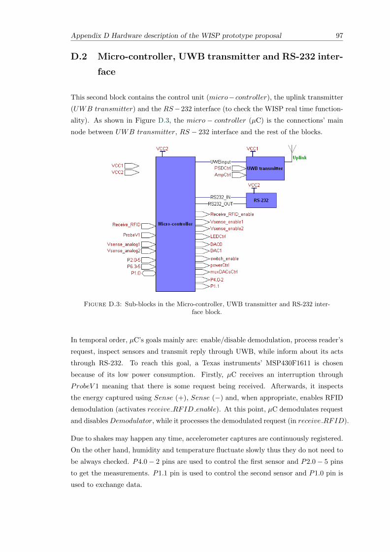
Appendix D Hardware description of the WISP prototype proposal 97
D.2 Micro-controller, UWB transmitter and RS-232 inter-
face
This second block contains the control unit (micro− controller), the uplink transmitter
(UWB transmitter) and the RS−232 interface (to check the WISP real time function-
ality). As shown in Figure D.3, the micro − controller (µC) is the connections’ main
node between UWB transmitter, RS − 232 interface and the rest of the blocks.
Figure D.3: Sub-blocks in the Micro-controller, UWB transmitter and RS-232 inter-face block.
In temporal order, µC’s goals mainly are: enable/disable demodulation, process reader’s
request, inspect sensors and transmit reply through UWB, while inform about its acts
through RS-232. To reach this goal, a Texas instruments’ MSP430F1611 is chosen
because of its low power consumption. Firstly, µC receives an interruption through
ProbeV 1 meaning that there is some request being received. Afterwards, it inspects
the energy captured using Sense (+), Sense (−) and, when appropriate, enables RFID
demodulation (activates receive RFID enable). At this point, µC demodulates request
and disablesDemodulator, while it processes the demodulated request (in receive RFID).
Due to shakes may happen any time, accelerometer captures are continuously registered.
On the other hand, humidity and temperature fluctuate slowly thus they do not need to
be always checked. P4.0− 2 pins are used to control the first sensor and P2.0− 5 pins
to get the measurements. P1.1 pin is used to control the second sensor and P1.0 pin is
used to exchange data.

98 Appendix D Hardware description of the WISP prototype proposal
Once the sensors are inspected, µC processes this data and builds the reply. Afterwards,
µC sends it to UWB transmitter, which is 1.8 V supplied, through UWBinput and
the subsequent level-translator. The last sends the modulated reply via uplink antenna,
while being adjusted by PSDCtrl and AmpCtrl pins.
After the reply is transmitted, the WISP “sleeps” again in order to save energy. There-
fore, obviously, µC and accelerometer are still “awake” to register all the shake fluctua-
tion.
After any action happened, µC sends a short description through RS − 232, using
RS232 IN and RS232 OUT , in order to test the WISP’s functionality.
These are all the sub-blocks referred to the “Micro-controller, UWB transmitter and
RS-232” block.
D.3 Sensors
Finally, the third block is described. It includes an Accelerometer, three Comparators
and a Humidity & Temperature SENSOR; all of them 3.3 V supplied (Figure D.4).
Figure D.4: Sub-blocks in the sensors block.
P4.0−2 pins are used to adjust theAccelerometer (Freescale Semiconductor’s MMA7260QT),
which yields the 3-axis measurements through its 13, 14 and 15 pins. These outputs
are low-pass filtered and hysteresis-compared. A Digital-to-Analog Converter (DAC)

Appendix D Hardware description of the WISP prototype proposal 99
output of the µC allow to reach a desired voltage level. So, these (DAC0 and DAC1)
outputs are used to set an analog voltage as a reference for the Comparators (National
semiconductor’s LMC6762). Due to the µC only has two DACs, these have to be shared
with an Analog switch which time-multiplexes its output in “Power supply & Demod-
ulator” block. As said, DACs are used to fix a reference and define the hysteresis region
where the µC registers the shakes measurements, ignoring insignificant values. Thus µC
is noticed through P2.1, P2.3 or P2.5 pins when the corresponding measurement of the
Accelerometer are greater than DAC0. Similarly, µC is noticed through P2.0, P2.2,
P2.4 pins when measurements are lower than DAC1; therefore, it stops registering.
On the other hand, the Humidity and Temperature SENSOR is placed. Sensirion’s
SHT15 is chosen. This is configured through the P1.0 and P1.1 pins and, when in-
spected, it sends the measured data through P1.0 pin as well. As said before, due to
humidity and temperature are not such fluctuating magnitudes, they do not have to be
inspected and registered continuously.
These are all the sub-blocks referred to the “Sensors” block.
D.4 Schematics
The following schematics show the complete board hardware; they are obtained by using
OrCAD Capture 15.7.

5
5
4
4
3
3
2
2
1
1
D D
C C
B B
A A
Receive_RFID_Enable
Receive_RFID
Vsense_analog2
Vsense_enable2
LEDCtrl
LEDCtrl
switch_enable muxDACsCtrlpowerCtrl
DAC0DAC1 PSDCtrlAmpCtrl
comp1 comp0
Vsense_analog1
Vsense_enable1
ProbeV1
VCC2
V2'
V1V2'V2''
V2'
VCC2 VCC1
V1
V1
V2
V1
V2
V1'
V1
VCC2
VCC2
Title
Size Document Number Rev
Date: Sheet of
Power supply, demodulator
A3
1 3Wednesday, September 22, 2010
Title
Size Document Number Rev
Date: Sheet of
Power supply, demodulator
A3
1 3Wednesday, September 22, 2010
Title
Size Document Number Rev
Date: Sheet of
Power supply, demodulator
A3
1 3Wednesday, September 22, 2010
ONLY 4 STAGES?
DOWN BRANCH?
ONLY 5 STAGES?ONLY 4 STAGES? ONLY 6 STAGES?
ONLY 5 STAGES? ONLY 6 STAGES?
Paper Battery
Current checkpoint
D15
SML-311UT
D15
SML-311UT
R3691kR3691k
R3 xR3 xCsU37pFCsU37pF
R4xR4x
U4
NLSV1T244
U4
NLSV1T244
VccA1
A2
GND3 OE* 4B 5
VccB 6
HSMS
D5
HSMS
D5
i1
o2
m3
R35150kR35150k
RB751S40T1RB751S40T1
CsU17pFCsU17pF
R13 xR13 x
L3
10uH
L3
10uH
TS5A3166TS5A3166
NO1
COM2
GND3 IN 4
V+ 5
CsU47pFCsU47pF
C120.1FC120.1F
Q4
NTK3134N
Q4
NTK3134N
HSMS
D8
HSMS
D8
i1
o2
m3
RB751S40T1RB751S40T1
CsU27pFCsU27pF
Q3NTK3134N
Q3NTK3134N
R7 xR7 x
CpD510pFCpD510pF
U8
NLSV1T244
U8
NLSV1T244
VccA1
A2
GND3 OE* 4B 5
VccB 6
R2666kR2666k
R24 xR24 x
NCP583
U13
NCP583
U13
CE1
GND2 Vout 3Vin 4
CpD410pFCpD410pF
R31100R31100
U7
S1000C20-I4T1
U7
S1000C20-I4T1
. 1
. 2.3
.4
HSMS
D14
HSMS
D14
i1
o2
m3
C93.3uFC93.3uF
R21 xR21 x
SMAconnectorSMAconnector
out+out-
R10 xR10 x
HSMS
D1
HSMS
D1
i1
o2
m3
CpU110pFCpU110pF
CD110uFCD110uF
R19xR19x
C11uFC11uF
HSMS
D13
HSMS
D13
i1
o2
m3
Q1
NTK3134N
Q1
NTK3134N
CsD27pFCsD27pF
HSMS
D4
HSMS
D4
i1
o2
m3
C61uFC61uF
C110.1FC110.1F
D16
SML-311YT
D16
SML-311YT
CpU310pFCpU310pF
R17xR17x
HSMS
D12
HSMS
D12
i1
o2
m3
R15xR15x
CsD37pFCsD37pF
R3010kR3010k
R11 xR11 x
CpD110pFCpD110pF
Q5
NTK3134N
Q5
NTK3134N
U15
MAX1606
U15
MAX1606
BATT1
FB 2Vcc3
GND 4
LX 5
LIM6
SHDN*7
SW8
R6xR6x
U9
ADG733
U9
ADG733
S2B1
S2A2
S3B3
D34
S3A5
EN*6
Vss7
GND8 A2 9A1 10A0 11
S1A 12S1B 13
D1 14D2 15
Vdd 16
HSMS
D11
HSMS
D11
i1
o2
m3
HSMS
D10
HSMS
D10
i1
o2
m3
L1
6.8nH
L1
6.8nH
R2733kR2733k
CsD57pFCsD57pF
HSMS
D7
HSMS
D7
i1
o2
m3
CsD47pFCsD47pF
C103.3uFC103.3uF
R9 xR9 x
HSMS
D9
HSMS
D9
i1
o2
m3
R14 xR14 x
CpD610pFCpD610pF
R25 xR25 x
CpU410pFCpU410pF
CsD67pFCsD67pF
CsU57pFCsU57pF
CpU510pFCpU510pF
R23 xR23 x
R12 xR12 x
R22 xR22 x
RB751S40T1RB751S40T1
HSMS
D3
HSMS
D3
i1
o2
m3
C1310uFC1310uF
U11
TS5A3166
U11
TS5A3166
NO1
COM2
GND3 IN 4
V+ 5
HSMS
D2
HSMS
D2
i1
o2
m3
U3
NCS2200SQ2T2G
U3
NCS2200SQ2T2G
_ 1
-2
+3
-4
+5
CsD17pFCsD17pF
C1447pFC1447pF
R1 xR1 x
R5 xR5 x
C210pFC210pF
CsU67pFCsU67pF
C51uFC51uF
U6
MAX828
U6
MAX828
OUT1
IN2
C1-3 GND 4
C1+ 5
NCP583
U14
NCP583
U14
CE1
GND2 Vout 3Vin 4
CpD210pFCpD210pF
HSMS
D6
HSMS
D6
i1
o2
m3
R20 xR20 x
CU110uFCU110uF
R8xR8x
CpD310pFCpD310pF
R18 xR18 x
Q2NTK3134N
Q2NTK3134N
R2933kR2933k
C710pFC710pF
CpU610pFCpU610pF
p1p2
MBRS0530MBRS0530
CpU210pFCpU210pF
R2866kR2866k
C83.3uFC83.3uF
R16 xR16 x
CsU77pFCsU77pF
C151uFC151uF
p2p3
p1
R2 xR2 x
CsD77pFCsD77pF
R32100R32100
L26.8nHL26.8nH

5
5
4
4
3
3
2
2
1
1
D D
C C
B B
A A
muxDACsCtrl
P4.2P4.1P4.0
UWBinput
LED
Ctr
l
P2.
0P
2.1
P2.
2P
2.3
P2.
4P
2.5
P6.3P6.4P6.5DAC0DAC1
P1.0
P1.4
Vse
nse_
anal
og1
Vse
nse_
enab
le2
Am
pCtr
lP
SD
Ctr
l
powerCtrl
switch_enable
RS232_TXRS232_RX
Receive_RFID_Enable
Vse
nse_
anal
og2
Vse
nse_
enab
le1
Rec
eive
_RF
IDP
robe
V1
RS232_OUT
RS232_IN
RS232_OUTRS232_IN
VCC2
VCC2
VCC1VCC2
VCC1
VCC2
VCC2
Title
Size Document Number Rev
Date: Sheet of
Microcontroller, UWB transmitter and RS-232
A3
2 3Wednesday, September 22, 2010
Title
Size Document Number Rev
Date: Sheet of
Microcontroller, UWB transmitter and RS-232
A3
2 3Wednesday, September 22, 2010
Title
Size Document Number Rev
Date: Sheet of
Microcontroller, UWB transmitter and RS-232
A3
2 3Wednesday, September 22, 2010
C1712pFC1712pF
U20
MAX232
U20
MAX232
C1+1
Vs+2
C1-3
C2+4
C2-5
Vs-6
T2OUT7
R2IN8 R2OUT 9T2IN 10T1IN 11
R1OUT 12R1IN 13
T1OUT 14GND 15VCC 16
X1
4MHz
X1
4MHz
UWB transmitterUWB transmitter
.1
.2
.3
.4
.5
.6
.7
.8
.9
.10
.11
.12
.13
.14
.15
.16
.17
.18
.19
.20
.21
.22
.23
.24
. 36
. 35
. 34
. 33
TX Out 32
TX Out 31
. 30
. 29
. 28
. 27
. 26
. 25
.48
.47
.46
.45
.44
VC
C 1
.843
VC
C A
nalo
g42
Inpu
t41
PS
D C
trl
40
Am
pltu
de C
trl
39
VC
C D
igita
l38
.37
R3710KR3710K
R441MR441M
X2
32KHz
X2
32KHz
U21
DE9male
U21
DE9male
DCD1RXD2TXD3DTR4GND5
DSR 6RTS 7CTS 8
RI 9
C2433pFC2433pF
SMAconnectorSMAconnector
out+out-
C1833pFC1833pF
C291uFC291uF
C2233pFC2233pF
C2512pFC2512pF
C2347nFC2347nF
R4610KR4610K
R3810KR3810K
C281uFC281uF
R401MR401M
C2112pFC2112pF
R421MR421M
R45
47K
R45
47K
R431MR431M
C261uFC261uF
C271uFC271uF
S1
switch
S1
switch
C20100nFC20100nF
C1612pFC1612pF
JTAG1
ML14
JTAG1
ML14
. 1
. 3
. 5
. 7
. 9
. 11
. 13
.2
.4
.6
.8
.10
.12
.14
R391MR391M
MSP430F1611MSP430F1611
DVcc1
P6.3/A32
P6.4/A43
P6.5/A54
P6.6/A6/DAC05
P6.7/A7/DAC1SVSIN6
Vref+7
XIN8
XOUT9
Veref+10
Vref-/Veref-11
P1.0/TACLK12
P1.1/TA013
P1.2/TA114
P1.3/TA215
P1.4/8MCLK16
P1.
5/T
A0
17
P1.
6/T
A1
18
P1.
7/T
A2
19
P2.
0/A
CLK
20
P2.
1/T
AIN
CLK
21
P2.
2/T
AO
UT
/TA
022
P2.
3/C
A0/
TA
123
P2.
4/C
A1/
TA
224
P2.
5/R
osc
25
P2.
6/A
DC
12C
LK/D
MA
E0
26
P2.
7/T
A0
27
P3.
0/S
TE
028
P3.
1/S
IMO
0/S
DA
29
P3.
2/S
OM
I030
P3.
3/U
CLK
0/S
CL
31
P3.
4/U
TX
D0
32
P3.5/URXD0 33P3.6 34P3.7 35
P4.0/TB0 36P4.1/TB1 37P4.2/TB2 38
P4.3 39P4.4 40P4.5 41P4.6 42
P4.7/TBCLK 43P5.0 44P5.1 45P5.2 46P5.3 47
P5.4/MCLK 48
P5.
5/M
CLK
49P
5.6/
AC
LK50
P5.
7/T
BO
UT
H/S
BS
OU
T51
XT
2IN
52X
T2O
UT
53T
DO
/TD
I54
TD
I/T
CLK
55
TC
K57
TM
S56
RS
T*/
NM
I58
P6.
0/A
059
P6.
1/A
160
P6.
2/A
261
AV
ss62
DV
ss63
AV
cc64
R411MR411M
C1910uFC1910uF
U19
NLSV1T244
U19
NLSV1T244
VccA1
A2
GND3 OE* 4B 5
VccB 6

5
5
4
4
3
3
2
2
1
1
D D
C C
B B
A A
P4.2P4.1
P4.0
P6.3
P6.4
P6.5
P2.0P6.3comp1
P2.1comp0P6.3
P2.4P6.5 P2.5
P6.5
P2.2P6.4 P2.3
P6.4
P1.0P1.4
comp1 comp0
comp1 comp0
VCC2
VCC2
VCC2
VCC2
VCC2
Title
Size Document Number Rev
Date: Sheet of
Accelerometer and humidity and temperature sensor
A4
3 3Wednesday, September 22, 2010
Title
Size Document Number Rev
Date: Sheet of
Accelerometer and humidity and temperature sensor
A4
3 3Wednesday, September 22, 2010
Title
Size Document Number Rev
Date: Sheet of
Accelerometer and humidity and temperature sensor
A4
3 3Wednesday, September 22, 2010
Current checkpoint
Current checkpoint
C381uFC381uF
C350.1uFC350.1uF
C3047nFC3047nF
C330.1uFC330.1uF
U23
LMC6762
U23
LMC6762
Out A1
In A-2
In A+3
V-4 In B+ 5In B- 6
Out B 7V+ 8
C310.1uFC310.1uF
C370.1uFC370.1uF
R47 1KR47 1K
U22
MMA7260QT
U22
MMA7260QT
g-Select11
g-Select22
Vdd3
Vss4
N/C
5
N/C
6
N/C
7
N/C
8
N/C 9N/C 10N/C 11
Sleep*/mode 12
Zou
t13
You
t14
Xou
t15
N/C
16
U24
LMC6762
U24
LMC6762
Out A1
In A-2
In A+3
V-4 In B+ 5In B- 6
Out B 7V+ 8
R5010KR5010K
R49 1KR49 1K
U25
LMC6762
U25
LMC6762
Out A1
In A-2
In A+3
V-4 In B+ 5In B- 6
Out B 7V+ 8
p1p2
U26
SHT15
U26
SHT15
GND 4DATA 3
SCK 2VDD 1
C320.1uFC320.1uF
C340.1uFC340.1uF
p1p2
C360.1uFC360.1uF
R48 1KR48 1K

Bibliography
[1] Majid Baghaei Nejad, Zhuo Zou, David S. Mendoza and Li-Rong Zheng,
“Remotely UHF-Powered Ultra Wideband RFID for Ubiquitous Wireless Identifica-
tion and Sensing”
[2] EPC Global, “Class-1 Generation-2 UHF RFID Protocal for Communications at
860 MHz - 960 MHz. Version 1.2.0 ”, October 2008
[3] “Ultra-Wideband (UWB) First Report and Order”. Federal Communications Com-
mission. Feb 2002.
[4] Zhuo Zou, M. Baghaei-Nejad, Li-Rong Zheng, “Digital Baseband Design for
UWB RFID. From specification to implementation”. Jan 2007
[5] C. Jae-Ryong and K. Jae-Hyun, “Novel anti-collision algorithms for fast object
identification in RFID system”, Parallel and Distributed Systems, 2005. Proceedings.
11th International Conference on, 2005, pp. 63-67 Vol. 2.
[6] Texas instruments, “MSP430x2xx Family - User’s guide”
[7] Texas instruments, “MSP430F2132 - Data sheet”
[8] Tektronix, “TCPA300/400 Amplifiers & TCP300/400 Series AC/DC Current
Probes - User Manual”
[9] Tektronix, “TCPA300/400 Amplifiers & TCP300/400 Series AC/DC Current
Probes - Service Manual”
[10] WISP, WISP wiki, http://wisp.wikispaces.com/. Accessed: 2010-02-06
[11] D. Sarmiento, S. Radiom, M. Baghaei-Nejad, G. Vandenbosch, H. Ten-
hunen, Li-Rong Zheng, G. Gielen, “A 4.11pJ/Pulse 3.1-10.6 GHz Transmitter-
Antenna Co-Designed I-UWB Front-End with Adjustable Bandwidth and Amplitude”
[12] B. Jamali, D. C. Ranasinghea, P. H. Colea, “Analysis of a UHF RFID CMOS
rectifier structure and input impedance characteristics”, School of Electrical & Elec-
tronic Engineering, Univ. of Adelaide, SA, Australia 5005
103

Bibliography BIBLIOGRAPHY
[13] John. F. Dickson, “On-chip High-Voltage Generation in Integrated Circuits Using
an Improved Multiplier Technique”, IEEE Journal of solid-state circuits, vol. sc-11,
no. 3, pp. 374-378 (1976)
[14] Raymond E. Barnett, Jin Liu, Steve Lazar, “A RF to DC Voltage Conversion
Model for Multi-Stage Rectifiers in UHF RFID Transponders”, IEEE Journal of
solid-state circuits, vol. 44, no. 2, pp. 354-364 (2009)
[15] T. H. Lee, “The Design of CMOS Radio-Frequency Integrated Circuits”, Cam-
bridge, U.K.: Cambridge Univ. Press, 2004