a reconfigurable stacked patch antenna for wireless power
TRANSCRIPT

Progress In Electromagnetics Research C, Vol. 29, 67–81, 2012
A RECONFIGURABLE STACKED PATCH ANTENNAFOR WIRELESS POWER TRANSFER AND DATATELEMETRY IN SENSORS
G. Yang1, M. R. Islam2, R. A. Dougal2, and M. Ali2, *
1Motorola Solutions, Holtsville, New York 11742, USA1Department of Electrical Engineering, University of South Carolina,Columbia, SC 29208, USA
Abstract—A reconfigurable stacked patch antenna is introduced forwireless power reception and data telemetry application in sensors.The proposed antenna operates at 5.8GHz with 9.4 dBi gain and 7.6%bandwidth. At a lower frequency 2.45 GHz the antenna operatesas a planar inverted-F antenna (PIFA) with 3.3 dBi gain and 2.0%bandwidth. Switching between the two regimes of operation is achievedusing PIN diodes. It is proposed that the antenna can be used forwireless power reception in sensors at 5.8 GHz and for data telemetryin between a sensor and a control station at 2.45GHz. The wirelesspower reception ability of this antenna was tested and verified bydeveloping a high efficiency schottky diode rectifying circuit. The RF-to-DC conversion efficiency was 85% for an input power density levelof 1 mW/cm2.
1. INTRODUCTION
Reconfigurable antennas have been widely explored in defense andcommercial wireless applications since a single aperture can beused to support multiple functions at separate frequency bands.Reconfigurable antennas can be realized by using MEMs or PIN diodeswitches. In [1] the geometry of an antenna was subdivided andMEMS switches were positioned at different locations of the antennato change the resonant frequency. In [2] a MEMS reconfigurableVee antenna was proposed where the beam was steered or shapedusing microactuators. In conjunction with MEMS switches forreconfigurability, stacked reconfigured bow-tie elements were proposed
Received 9 February 2012, Accepted 17 April 2012, Scheduled 1 May 2012* Corresponding author: Mohammod Ali ([email protected]).

68 Yang et al.
by Bernhard et al. [3] for space based radar applications. A multi-element miniature antenna was proposed in [4] which can operateat multiple frequency bands using MEMS switches. Reconfigurablepatch antennas with switchable slots using PIN diodes were introducedin [5, 6]. A planar VHF reconfigurable slot antenna was loaded withmultiple PIN diode switches to achieve frequency switching from 550 to900MHz [7]. In [8] a reconfigurable slot antenna allowing polarizationswitching was presented. Other reconfigurable antennas can be foundin [9, 10]. Earlier we proposed a reconfigurable antenna for dual-frequency operation for satellite and land mobile radio communicationapplications at 2 GHz and 450 MHz, respectively [11]. An excellentreview on reconfigurable antennas can be found in [12, 13]. In thispaper, we propose a reconfigurable stacked microstrip patch antennaintegrated with a rectifier that can function as a wideband, high gainantenna for wireless power reception in sensors at 5.8GHz and as adata telemetry antenna at 2.45GHz for communication in between asensor and a local base station.
Previously we presented this concept using simulation resultsin [14]. In this work, we demonstrate the practical realization ofthat concept. Along with experimental patch and PIN diode switchmeasurement data measured results of wireless power transfer usinga rectenna at 5.8 GHz are also presented when the rectenna is placedinside concrete samples.
Wireless power transmission in the 5–6 GHz band has been studiedbefore in [15–24] primarily because of the band being unlicensed andthat it allows larger antenna effective apertures resulting in higherantenna gain. Earlier wireless power transmission (at 5.7 GHz) to aburied sensor antenna in concrete was demonstrated in [22]. This wasdone considering such a scheme to charge the battery of a smart bridgehealth monitoring sensor.
Wireless sensors are becoming crucial for many applicationsranging from infrastructure monitoring to power systems faultdiagnostics. Sensors can detect a fault or problem and notify aninterrogator intermittently or on a continuous basis. It is well knownthat once embedded inside a difficult to reach area (such as concrete)high data rate active sensors must be replenished with power wirelessly.Efficient rectenna elements if integrated with the wireless sensors canreceive RF power and convert that to DC to drive the sensor circuitry.Since the sensor also needs to communicate with a nearby controlstation the data communication link must be established at anotherfrequency band. In this work, we consider the 2.45 GHz band for thedata telemetry function. Although a dual frequency rectenna operatingat 2.45GHz and 5.8GHz was reported in [20] the scheme requires a
Progress In Electromagnetics Research C, Vol. 29, 2012 69
reflector plate at a distance of 17 mm from the antenna which makesthe overall required volume quite large for sensor applications. Onthe other hand, the dual-frequency rectenna in [21] suffers from lowantenna gain (3.7 dBi at 5.8 GHz).
By contrast, in this work, the stacked patch antenna whenreconfigured using PIN diode switches operates as a planar inverted-F antenna [25–28] at 2.45 GHz and supports data communicationbetween a sensor and a control station. And when reconfigured ata second frequency (5.8 GHz) works as a high gain efficient rectennathat can receive wireless power to charge a sensor battery. Thereconfigurable antenna has an overall dimension of 100 × 80 × 6 mm3
(including the rectifying circuit).
2. ANTENNA DESIGN
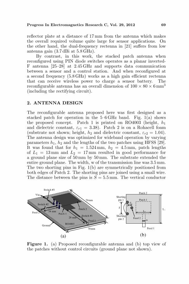
The reconfigurable antenna proposed here was first designed as astacked patch for operation in the 5–6 GHz band. Fig. 1(a) showsthe proposed concept. Patch 1 is printed on RO4003 (height, h1
and dielectric constant, εr1 = 3.38). Patch 2 is on a Rohacell foam(substrate not shown; height, h2 and dielectric constant, εr2 = 1.04).The antenna design was optimized for wideband operation by varyingparameters h1, h2 and the lengths of the two patches using HFSS [29].It was found that for h1 = 1.524mm, h2 = 4.5mm, patch lengthsof L1 = 13 mm and L2 = 17 mm resulted in good performance fora ground plane size of 50mm by 50 mm. The substrate extended theentire ground plane. The width, w of the transmission line was 3.5 mm.The two shorting pins in Fig. 1(b) are symmetrically positioned fromboth edges of Patch 2. The shorting pins are joined using a small wire.The distance between the pins is S = 5.5mm. The vertical conductor
Ground
Patch 1
Patch 2
Switch #1
Via
RO4003
(a) (b)
70 mm
70 mm
Switch #2
Switch #3
S
Shorting pin 1
Patch 2
d
Shorting pin 2 Feed 2
Patch 1
L 2L1
Feed 1
Feed 1
Feed 2
w 28 mm
34 mm
Figure 1. (a) Proposed reconfigurable antenna and (b) top view ofthe patches without control circuits (ground plane not shown).

70 Yang et al.
for Feed 2 is located d = 0.8 mm inside from the edge of the patch.The diameter of the feed and shorting pin conductors is 0.5 mm.
The reconfigurable operation of the proposed antenna can beexplained from Fig. 1(a). There are three switches (1, 2, and 3) thatcontrol Feed 1, Feed 2, and the shorting pins. When Feed 1 is activated(switch 1 on), Feed 2 and the shorting pins are deactivated (switches2 and 3 are off), the antenna operates as a stacked microstrip patch ataround 5.8 GHz with directional high gain beam. Next, when Feed 1is de-activated (switch 1 is off) and Feed 2 and the shorting pins areactivated (switches 2 and 3 are on) the antenna operates at 2.45GHzwith nearly omnidirectional radiation pattern.
Before having two shorting pins we observed that with only oneshorting pin the PIFA resonant frequency was lower than 2.45GHz. Toensure PIFA operation at around 2.45 GHz an additional shorting pinwas added. Simulations were conducted to determine the optimumvalue for S. The effect of the pins and Feed 2 on stacked patchperformance at 5.8 GHz was also investigated.
3. RESULTS
3.1. Reconfigurable Antenna without Control Circuits
First, operations in the stacked patch and PIFA regimes were studiedwithout any PIN diode control circuits. Thus the switches were idealshort when activated and ideal open when deactivated. Two cases wereconsidered:
Case 1: In the stacked patch operation (see Fig. 2(a)) Feed 1 wasactivated while Feed 2 and the shorting pins were deactivated. Thevertical elements for Feed 2 and the two pins were connected to Patch 2located on the top. In the bottom Feed 2 and the shorting pins touchedthe top surface of the RO4003 substrate. These vertical elements weremodeled using cylindrical conductors (0.5 mm diameter).
Lumped gap
source
(b)(a)
RO4003 Shorted to
ground
Patch 1
Patch 2 Shorted to ground
Figure 2. (a) Stacked patch mode and (b) PIFA mode without controlcircuits. L1 = 13 mm, L2 = 17 mm, S = 5.5 mm, d = 0.8mm, groundplane: 50× 50 mm2.

Progress In Electromagnetics Research C, Vol. 29, 2012 71
(a) (b)
Figure 3. Simulated and measured S11 data (dB) without controlcircuits; (a) stacked patch mode and (b) PIFA mode. L1 = 13 mm,L2 = 17 mm, S = 5.5mm, d = 0.8mm, ground plane: 50× 50mm2.
PIN Diode
Gnd
C RFout
RFin C
L L
R
+Vcc
C=8.1 pF
L=22 nH
R=2.1 K
C=3 pF
L=3.2 nH
R=2.1 KΩ
For2.45 GHz PIN Diode (HSMP-389B)
For 5.8 GHz PI N Diode (MPP4203)
Ω
Figure 4. PIN diode control circuit.
Case 2: In the PIFA operation (see Fig. 2(b)) Feed 1 wasdeactivated while Feed 2 was activated and the shorting pins weredirectly connected to the ground below the RO4003 substrate.Simulated and measured S11 data for the stacked patch are shownin Fig. 3(a) (Case 1). Measured bandwidth extends from 5.5 to6.4GHz (−10 dB). There is good agreement between the measured andsimulated data. Fig. 3(b) shows the PIFA data (Case 2). Again, thesimulated and measured data agree well. Measured bandwidth extendsfrom 2.42 to 2.51 GHz.
3.2. Reconfigurable Antenna with Control Circuits
In this section, we present the results of the reconfigurable antennacontaining the PIN diode switching circuits. A schematic diagramrepresenting the switch is shown in Fig. 4. Two DC blocking Capacitors(C), two RF choke inductors (L), and a resistor (R) were usedwith PIN diodes to develop the switches. Switches #2 and #3(2.45GHz operation) were fabricated using HSMP-389B diodes from

72 Yang et al.
(a) (b)
Figure 5. Simulated return loss including simple models for PIN diodecontrol circuits with Patch 2 size (L2) as the parameter; (a) PIFAmode, (b) patch mode. Other parameters: L1 = 13 mm, S = 5.5mm,d = 0.8mm.
Avago Technologies. Switch #1 (5.8 GHz operation) was fabricatedusing an MPP4203 diode from Microsemi. More details of thePIN diode switching circuits are available in [30]. At 2.45 GHzthe measured insertion loss and isolation were 0.5 dB and 11 dB,respectively. Similarly at 5.8 GHz the measured insertion loss andisolation were 1.3 dB and 9.5 dB, respectively. The insertion loss andisolation are governed by the diode on resistance and off capacitance.It is expected that a 10 dB isolation will be adequate for embeddedsensing applications primarily because embedded sensors will not havenearby outside interferers and the amount of power used here willbe quite small to cause interference to other wireless devices even ifthey are nearby. If increased isolation is required very low capacitancediodes, transistors, or MEMs switches can be used.
Two simulation models were developed in HFSS to study theantenna performance with the switches. To accommodate theswitching circuits the substrate and the ground plane sizes wereincreased from 50 × 50mm2 to 70 × 70mm2. In the stacked patchoperation, switch #1 (Fig. 1(a)) was ON while the other two switcheswere OFF. All DC blocking capacitors associated with switch #1were considered short while the inductors and the resistor associatedwith switch #1 were considered open. Opposite was the case for thePIFA mode. These simulations basically illustrate the effects of thetransmission lines associated with the switches, the wire connectingthe two shorting pins and the larger ground plane.
Simulated S11 data for the stacked patch and the PIFA modes forthese scenarios are shown in Figs. 5(a) and (b) respectively. In thestacked patch mode, with the original dimensions (L2 = 17 mm forPatch 2) the resonant frequency shifts from 6.0 to 6.3 GHz. Similarly,

Progress In Electromagnetics Research C, Vol. 29, 2012 73
Figure 6. Simulated input resistance and reactance in the PIFA modewith and without the modification of the microstrip line Feed 2 shownin Fig. 6.
in the PIFA mode the resonant frequency moves to 2.61 GHz from2.47GHz. To compensate for this, Patch 2 size was increased to19mm. For L2 = 19mm, the stacked patch mode operates from 5.52to 6.2 GHz. The PIFA mode operates at 2.48GHz but the S11 level ispoor.
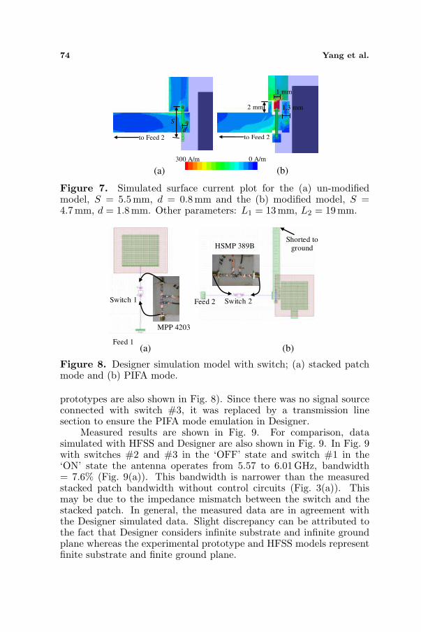
To improve the PIFA S11 level studies of the input resistance andreactance of the PIFA mode (Fig. 6) show that the input reactanceat 2.45 GHz is about +j47Ω. To reduce this reactance, modificationswere made near the PIFA feed. Figs. 7(a) and (b) also show the surfacecurrent plots at 2.45 GHz for the un-modified and modified feed models.Clearly in Fig. 7(b) there is more current concentration than the un-modified feed in Fig. 7(a). This translates into additional capacitancewhich causes the input reactance to decrease from +j47 Ω to +j2.9Ω(Fig. 6). As shown in Fig. 7(b) the modified feed had S= 4.7 mmand d = 1.8mm compared to S = 5.5mm and d = 0.8mm for the un-modified feed. These adjustments also increased the input resistancefrom 11.2 Ω to 50.3 Ω. Based on these modifications we fabricatedour final reconfigurable antenna prototype and measured it before therectifying circuitry was added.
To understand the effect of the switches on the antenna S11 andgain, we also modeled and simulated the reconfigurable antenna inDesigner [29]. Figs. 8(a)–(b) show these models. First, we measuredthe S parameters of the 2.45 GHz and 5.8 GHz switching circuitsand then saved those data in two separate s2p files which wereloaded in Designer. Note that, in Designer simulations there wereno transmission lines connected with the feeds (Figs. 8(a)–(b)). Thiswas done to eliminate the delay associated with the transmissionlines present in the fabricated prototype of the switching circuits (the
74 Yang et al.
2
0.6
300 A/m
(a) (b)
2 mm
1 mm
1.3 mm
0 A/m
S
d
to Feed 2 to Feed 2
Figure 7. Simulated surface current plot for the (a) un-modifiedmodel, S = 5.5 mm, d = 0.8mm and the (b) modified model, S =4.7mm, d = 1.8mm. Other parameters: L1 = 13 mm, L2 = 19 mm.
(a) (b)
Switch 1 Switch 2
Feed 1
Feed 2
Shorted to ground HSMP 389B
MPP 4203
Figure 8. Designer simulation model with switch; (a) stacked patchmode and (b) PIFA mode.
prototypes are also shown in Fig. 8). Since there was no signal sourceconnected with switch #3, it was replaced by a transmission linesection to ensure the PIFA mode emulation in Designer.
Measured results are shown in Fig. 9. For comparison, datasimulated with HFSS and Designer are also shown in Fig. 9. In Fig. 9with switches #2 and #3 in the ‘OFF’ state and switch #1 in the‘ON’ state the antenna operates from 5.57 to 6.01 GHz, bandwidth= 7.6% (Fig. 9(a)). This bandwidth is narrower than the measuredstacked patch bandwidth without control circuits (Fig. 3(a)). Thismay be due to the impedance mismatch between the switch and thestacked patch. In general, the measured data are in agreement withthe Designer simulated data. Slight discrepancy can be attributed tothe fact that Designer considers infinite substrate and infinite groundplane whereas the experimental prototype and HFSS models representfinite substrate and finite ground plane.

Progress In Electromagnetics Research C, Vol. 29, 2012 75
(a) (b)
Figure 9. Measured and simulated impedance bandwidth of thereconfigurable antenna with the PIN diode circuits; (a) stacked patchand (b) PIFA mode. L1 = 13 mm, L2 = 19 mm, S = 4.7mm,d = 1.8mm, Feed 2 modified.
(a) (b)
(c) (d)
Eφ
Eθ
Figure 10. Simulated normalized radiation patterns with simple PINdiode control circuit models; (a) E plane (φ = 0) at 5.8 GHz, (b) Hplane (φ = 90) at 5.8 GHz, (c) φ = 0 at 2.45 GHz, and (d) φ = 90at 2.45 GHz.

76 Yang et al.
With switch #1 in the ‘OFF’ state and switches #2 and #3 in the‘ON’ state we have the PIFA mode operation for which the measureddata are shown in Fig. 9(b). The bandwidth extends from 2.43 to2.48GHz (2.0%). The measured data agree well with the simulations.The levels of measured S11 compare quite well with those obtainedusing Designer. Slight detuning in the Designer simulated data isobserved because designer considers infinite substrate and infiniteground plane.
Simulated radiation patterns (using HFSS) of the PIFA and thestacked patch modes (L1 = 13 mm, L2 = 19mm, S = 4.7mm,d = 1.8mm, feed and shorting pin region modified) are shown inFig. 10. Figs. 10(a) (φ = 0, E plane) and 10(b) (φ = 90, H plane)illustrate the patterns at 5.8 GHz. The peak realized gain is 9.4 dBi notincluding the switch insertion loss. To determine the effect of switchloss on antenna gain degradation two simulations were performed inDesigner one with the switch and the other without the switch. Peakgain decreased by 1.3 dB with the switch. Thus the peak gain in thestacked patch mode is 8.1 dBi. Fig. 10(c) (φ = 0) and 10(d) (φ = 90)depict the patterns (HFSS) at 2.45GHz, for the PIFA mode. They arestandard PIFA radiation patterns with 3.3 dBi peak gain not includingswitch losses. Designer simulations show 0.4 dB gain reduction at2.45GHz. Thus, the peak gain in the PIFA mode is 2.9 dBi.
4. APPLICATION OF RECONFIGURABLE ANTENNAFOR WIRELESS POWER TRANSMISSION
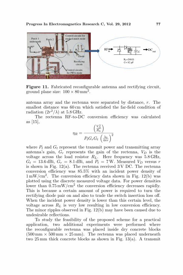
To test the wireless power reception ability of the proposed antenna,a rectifying circuit was fabricated and connected to the stackedreconfigurable patch as shown in Fig. 11. The rectifier consisted of anHSMS-2862 microwave Si Schottky detector diode pair (Rs = 6.0Ω,Cj0 = 0.18 pF, Vbi = 0.65V, and VB = 7 V for each diode), a capacitorC and a load resistor RL. The equivalent circuit parameters are givenin [15]. The diode pair was connected as a voltage-doubler to increasethe output DC voltage (VD). A quarter wave length transformer T1
(1.95mm × 7mm) and a microstrip line T2 (0.94mm × 3mm) wereused between the diode pair and the antenna for impedance matching(Fig. 11). Detail description of the rectifying circuit can be foundin [30].
The performance of the rectenna was measured by illuminatingit with a four-element microstrip patch antenna array (13.6 dBi gain)described in [22] which was connected to a high-power amplifier (7 W,5.3–5.9GHz) and a microwave signal generator. The received voltageat the rectenna was measured using a voltmeter. The transmitter
Progress In Electromagnetics Research C, Vol. 29, 2012 77
Ante
nna
Rectifying circuit
Control circuits for PIFA mode
Control circuits for
stacked patch mode Patch 2 Patch 1
underneath
C RL
Diode T2
T1 ϕ=0
ϕ=90ο
DCout
RL C
RFin
C= 82 pF
RL=200Ω
ο
Figure 11. Fabricated reconfigurable antenna and rectifying circuit,ground plane size: 100× 80mm2.
antenna array and the rectenna were separated by distance, r. Thesmallest distance was 60 cm which satisfied the far-field condition ofradiation (2r2/λ) at 5.8 GHz.
The rectenna RF-to-DC conversion efficiency was calculatedas [15],
ηR =
(V 2
DRL
)
PtGrGt
(λ04πr
)2
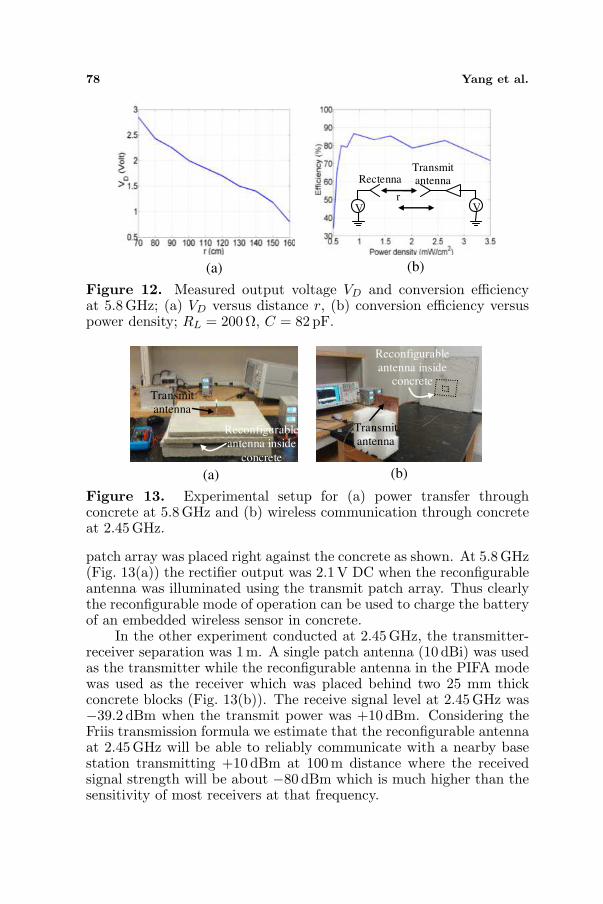
where Pt and Gt represent the transmit power and transmitting arrayantenna’s gain, Gr represents the gain of the rectenna, VD is thevoltage across the load resistor RL. Here frequency was 5.8GHz,Gt = 13.6 dBi, Gr = 8.1 dBi, and Pt = 7 W. Measured VD versus ris shown in Fig. 12(a). The rectenna received 3V DC. The rectennaconversion efficiency was 85.5% with an incident power density of1mW/cm2. The conversion efficiency data shown in Fig. 12(b) wasplotted using the discrete measured voltage data. For power densitieslower than 0.75 mW/cm2 the conversion efficiency decreases rapidly.This is because a certain amount of power is required to turn therectifying diode pair on and also to trade the switch insertion loss off.When the incident power density is lower than this certain level, thevoltage across RL is very low resulting in low conversion efficiency.The minor ripples observed in Fig. 12(b) may have been caused due toundesirable reflections.
To study the feasibility of the proposed scheme for a practicalapplication, two additional experiments were performed wherethe reconfigurable rectenna was placed inside dry concrete blocks(500mm × 500mm × 25mm). The rectenna was placed underneathtwo 25 mm thick concrete blocks as shown in Fig. 13(a). A transmit
78 Yang et al.
(a) (b)
Transmit
antenna Rectenna
V
r V
Figure 12. Measured output voltage VD and conversion efficiencyat 5.8 GHz; (a) VD versus distance r, (b) conversion efficiency versuspower density; RL = 200 Ω, C = 82 pF.
(a) (b)
Transmit
antenna
Reconfigurable
antenna inside
concrete
Transmit
antenna
Reconfigurable
antenna inside concrete
Figure 13. Experimental setup for (a) power transfer throughconcrete at 5.8GHz and (b) wireless communication through concreteat 2.45 GHz.
patch array was placed right against the concrete as shown. At 5.8 GHz(Fig. 13(a)) the rectifier output was 2.1 V DC when the reconfigurableantenna was illuminated using the transmit patch array. Thus clearlythe reconfigurable mode of operation can be used to charge the batteryof an embedded wireless sensor in concrete.
In the other experiment conducted at 2.45GHz, the transmitter-receiver separation was 1 m. A single patch antenna (10 dBi) was usedas the transmitter while the reconfigurable antenna in the PIFA modewas used as the receiver which was placed behind two 25 mm thickconcrete blocks (Fig. 13(b)). The receive signal level at 2.45GHz was−39.2 dBm when the transmit power was +10 dBm. Considering theFriis transmission formula we estimate that the reconfigurable antennaat 2.45 GHz will be able to reliably communicate with a nearby basestation transmitting +10 dBm at 100 m distance where the receivedsignal strength will be about −80 dBm which is much higher than thesensitivity of most receivers at that frequency.

Progress In Electromagnetics Research C, Vol. 29, 2012 79
5. CONCLUSION
The study and design of a stacked reconfigurable microstrip patchantenna are presented. Using PIN diode switches it is demonstratedthat a stacked microstrip patch can be reconfigured to support twodistinctly different operating frequency bands with varying bandwidthand radiation patterns. The stacked patch is suitable for wirelesspower reception in sensors. The PIFA is suitable for wireless datacommunication between sensors or sensor and a control station due toits balanced azimuthal pattern coverage. The reconfigurable antennawhen integrated with a rectifying circuit can receive and convert RFenergy with a conversion efficiency of 85%. The reconfigurable antennacan successfully receive power and communicate with nearby basestation when it is embedded in concrete.
ACKNOWLEDGMENT
This work was supported in part by the US Office of Naval Researchunder grant No. 0014-02-1-0623.
REFERENCES
1. Weedon, W. H. and W. J. Payne, “MEMS-switched reconfigurablemulti-band antenna: Design and modeling,” Proceedings of the1999 Antenna Applications Symposium, Monticello, IL, Sep. 15–17, 1999.
2. Chiao, J.-C., Y. Fu, I. M. Chio, M. D. Lisio, and L. Y. Lin,“MEMS reconfigurable vee antenna,” IEEE MTT-S Symp. Dig.,1999.
3. Bernhard, J. T., R. Wang, and P. Mayes, “Stacked reconfigurableantenna elements for space based radar applications,” IEEEAntennas Propagat. Symp. Dig., Vol. 1, 158–161, 2001.
4. Jofre, L., B. A. Cetiner, and F. de Falviss, “Miniature multi-element antenna for wireless communications,” IEEE Trans.Antennas Propagat., Vol. 50, 658–669, May 2002.
5. Yang, F. and Y. Rahmat-Samii, “Patch antenna with switchableslot (PASS): Dual frequency operation,” Microwave Opt. Technol.Lett., Vol. 31, No. 3, 165–168, Nov. 2001.
6. Yang, F. and Y. Rahmat-Samii, “A reconfigurable patch antennausing switchable slots for circular polarization diversity,” IEEEMicrowave Wireless Component Lett., Vol. 12, 96–98, Mar. 2002.
80 Yang et al.
7. Peroulis, D., K. Sarabandi, and L. P. B. Katehi, “A planar VHFreconfigurable slot antenna,” IEEE Antennas Propagat. Symp.Dig., Vol. 1, 154–157, 2001.
8. Fries, M. K., M. Grani, and R. Vahldieck, “A reconfigurable slotantenna with switchable polarization,” IEEE Microwave WirelessComponent Lett., Vol. 13, 490–492, Nov. 2003.
9. Langer, J. C., J. Zou, C. Liu, and J. T. Bernhard, “Micromachinedreconfigurable out-of-plane microstrip patch antenna using plasticdeformation magnetic actuation,” IEEE Microwave WirelessComponent Lett., Vol. 13, 120–122, Mar. 2003.
10. Nair, S. V. S. and M. J. Ammann, “Reconfigurable antenna withelevation and azimuth beam switching,” IEEE Antennas WirelessPropagat. Lett., Vol. 9, 367–370, 2010.
11. Kunda, V. K., M. Ali, and H. S. Hwang, “A tunable stacked mi-crostrip patch antenna for directional and omnidirectional links,”Proc. IEEE Antennas and Propagation Society International Sym-posium and URSI/USNC Meeting, Monterey, CA, Jun. 2004.
12. Bernhard, J. T., “Reconfigurable antennas,” The Wiley Encyclo-pedia of RF and Microwave Engineering, K. Chang, Editor, 2005.
13. Bernhard, J. T., “Reconfigurable antennas,” Antenna EngineeringHandbook, J. Volakis, Editor, 4th Edition, McGraw Hill, 2007.
14. Yang, G., M. Ali, and R. A. Dougal, “A multi-functional stackedpatch antenna for wireless power beaming and data telemetry,”Proc. IEEE Antennas and Propagat. Soc. Int. Sym. Dig., Vol. 2A,359–362, Washington, DC, Jul. 2005.
15. Strassner, B. and K. Chang, “5.8 GHz circularly polarizedrectifying antenna for wireless microwave power transmission,”IEEE Trans. Microwave Theory Tech., Vol. 50, 1870–1876,Aug. 2002.
16. Strassner, B. and K. Chang, “5.8GHz circularly polarized dual-rhombic-loop traveling-wave rectifying antenna for low power-density wireless power transmission applications,” IEEE Trans.Microwave Theory Tech., Vol. 51, 1548–1553, May 2003.
17. Chin, C. K., Q. Xue, and C. H. Chan, “Design of a 5.8-GHzrectenna incorporating a new patch antenna,” IEEE AntennasWireless Propagat. Lett., Vol. 4, 175–178, 2005.
18. Ren, Y. and K. Chang, “5.8GHz circularly polarized dual-dioderectenna and rectenna array for microwave power transmission,”IEEE Trans. Microwave Theory Tech., Vol. 54, 1495–1502,Apr. 2006.

Progress In Electromagnetics Research C, Vol. 29, 2012 81
19. Radiom, S., M. B. Nejad, K. M. Aghdam, G. A. E. Vanden-bosch, L. Zheng, and G. G. E. Gielen, “Far-field on-chip anten-nas monolithically integrated in a wireless-powered 5.8-GHz down-link/UWB uplink RFID tag in 0.18-µm standard CMOS,” IEEEJournal. Solid State Cir., Vol. 45, 1746–1758, Sep. 2010.
20. Suh, Y. and K. Chang, “A high-efficiency dual-frequency rectennafor 2.45- and 5.8-GHz wireless power transmission,” IEEE Trans.Microwave Theory Tech., Vol. 50, 1784–1789, Jul. 2002.
21. Heikkinen, J. and M. Kivikoski, “A novel dual-frequency circularlypolarized rectenna,” IEEE Antennas Wireless Propagat. Lett.,Vol. 2, 330–333, 2003.
22. Shams, K. M. Z. and M. Ali, “Wireless power transmission to aburied sensor in concrete,” IEEE Sensors Journal, Vol. 7, 1573–1577, Dec. 2007.
23. Ali, M., G. Yang, and R. A. Dougal, “A new circularlypolarized rectenna for wireless power transmission and datacommunication,” IEEE Antennas Wireless Propagat. Lett., Vol. 4,205–208, Jul. 2005.
24. Ali, M., G. Yang, and R. Dougal, “Miniature circularly polarizedrectenna with reduced out of band harmonics,” IEEE Antennasand Wireless Propagat. Lett., Vol. 5, 107–110, 2006.
25. Rowell, C. R. and R. D. Murch, “A capacitively loaded PIFAfor compact mobile telephone handsets,” IEEE Trans. AntennasPropagat., Vol. 45, 837–842, May 1997.
26. Virga, K. L. and Y. Rahmat-Samii, “Low-profile enhanced-bandwidth PIFA antennas for wireless communications packag-ing,” IEEE Trans. Microwave Theory Tech., Vol. 45, 1879–1888,Oct. 1997.
27. Waterhouse, R. B., S. D. Targonski, and D. M. Kokotoff,“Design and performance of small printed antennas,” IEEE Trans.Antennas Propagat., Vol. 46, 1629–1633, Nov. 1998.
28. Karmakar, N. C., “Shorting strap tunable stacked patch PIFA,”IEEE Trans. Antennas Propagat., Vol. 52, 2877–2884, Nov. 2004.
29. Ansoft Corporation, Available: www.ansoft.com.30. Yang, G., “Conformal multi-functional antennas and rectifying
circuits for wireless communication and microwave powerbeaming,” Ph.D. Dissertation, University of South Carolina, 2005.