a review of gallium nitride leds for multi gigabit per ... · harald haas4, ian m. watson3, dominic...
TRANSCRIPT

1
A review of Gallium Nitride LEDs for
multi-gigabit-per-second visible light data
communications Sujan Rajbhandari1,2, Jonathan J. D. McKendry3, Johannes Herrnsdorf3, Hyunchae Chun2, Grahame Faulkner2,
Harald Haas4, Ian M. Watson3, Dominic O’Brien2, and Martin D. Dawson3
1School of Computing, Electronics and Mathematics, Coventry University, Coventry, CV1 2JH, United Kingdom
2Department of Engineering Science, University of Oxford, Oxford, OX1 3PJ, United Kingdom
3Institute of Photonics, Department of Physics, University of Strathclyde, Glasgow, G1 1RD, United Kingdom
4Institute for Digital Communications, Li-Fi R&D Centre, University of Edinburgh, Edinburgh, EH9 3JL, United
Kingdom
Abstract
The field of visible light communications (VLC) has gained significant interest over the last decade,
in both fibre and free-space embodiments. In fibre systems, the availability of low cost plastic optical fibre
(POF) that is compatible with visible data communications has been a key enabler. In free-space
applications, the availability of hundreds of THz of the unregulated spectrum makes VLC attractive for
wireless communications. This paper provides an overview of the recent developments in VLC systems
based on gallium nitride (GaN) light-emitting diodes (LEDs), covering aspects from sources to systems.
The state-of-the-art technology enabling bandwidth of GaN LEDs in the range of >400 MHz is explored.
Furthermore, advances in key technologies, including advanced modulation, equalisation, and
multiplexing that have enabled free-space VLC data rates beyond 10 Gb/s are also outlined.

2
1 Introduction
The evolution of computing, consumer electronics and mobile communications technologies is leading to
an exponential increase in end-user data requirements. Reports by Cisco, for example, predict that there will be
a nine-fold increase in mobile communications traffic from 2014 to the end of 2020, almost doubling every two
years [1]. If the global traffic volume increases at the current rate, there will soon be ‘a spectrum crisis’ as radio
frequency (RF) technology cannot keep pace with the demand [2]. It is also very unlikely that a single
communication technology can support these growing data requirements in all places at all times. Hence, future
generations of networks must support the co-existence and cooperation of different wireless technologies (RF,
millimetre wave, and optical wave) [3]. With the evolution of the new wireless communication standards like
the fourth generation (4G) and fifth generation (5G) networks, the available RF spectra are efficiently utilized
by using advanced signal processing concepts such as massive multiple-input multiple-output (MIMO) systems
and shrinking cell size leading to femtocells. In parallel, untapped frequencies at millimetre and nanometre
wavelengths are also being considered. It is widely expected that visible light communications (VLC) systems
and their extension to fully networked, bi-directional multiuser wireless systems referred to as LiFi ( see [4] for
detail) will play a key part in 5G-and-beyond connectivity, especially for indoor environments [2], [5], [6].
Indoor lighting has also undergone a revolution with the recent advances in solid-state lighting (SSL)
devices based on visible light emitting diodes (LEDs). Incandescent bulbs with an extremely low efficiency of
13-18 lumens per watt are being phased out. The compact fluorescent light (CFL) which was introduced in the
1990s offers a better energy conversion (55-70 lumens per watt). However, these efficiencies have recently been
superseded by LED and laser diode (LD) based lighting. The average efficiency of Gallium-Nitride LEDs is
higher than 100 lumens per Watt and is expected to reach 200 lumens per Watt by 2020 [7], [8]. Besides higher
efficiencies, the LEDs also offer other advantages including a long operational lifetime (up to 50,000 hours),
compact form factor, no emission of harmful ultraviolet or infrared radiation, mercury-free operation and a low
maintenance cost. Additionally, the manufacturing cost of LEDs is dropping as the technology continues to
mature for mass production, making LED based illumination economical in comparison to CFLs over its
lifetime. Hence, the adoption of LED-based illumination is rising steadily [9], [10].
The popularity of SSL-based illumination has created a unique opportunity as each light bulb can
potentially serve as a communication hotspot. Unlike traditional lighting devices, SSL devices can be modulated
at a rate imperceptible to the human eye. This has paved the way for the dual function of illumination and
communication using LEDs, in principle enabling communication at minimal extra cost and energy
consumption [11]. The wide availability of lighting infrastructure and the feasibility of achieving
communication rates beyond 100’s of Mb/s makes VLC a cost effective and attractive complementary technique
to RF technology.
The first reported VLC system based on a visible LED was in 1999 [12] when Pang et al. used
modulated LED traffic lights for broadcasting audio and other information. Tanaka et al. adopted LEDs for
illumination and communication in the early 2000s [13]. Interest in VLC now is growing rapidly with a number
of practical demonstrations. In Japan, the visible light communication consortium (VLCC) [14] was formed in
2003 which is now superseded by the visible light communication association (VLCA) [15]. A number of key
technologies were demonstrated in the European Union funded ‘hOME Gigabit Access’ project (OMEGA)
project [16]. Recently, the UK government funded Ultra-parallel visible light communications (UP-VLC) [17]
project has demonstrated a 10 Gbits/s VLC system [18]. In parallel to these research activities, there have been
efforts to establish a VLC standard and IEEE802.15.7 was proposed in 2011 [19], [20]. A task group on short-
range optical wireless communication (OWC) was formed in 2015 to revise the IEEE 802.15.7 standard [21].
Early VLC demonstrations were based on conventional chip, broad-area (0.1-1mm2) Gallium Nitride
(GaN) LEDs originally developed for lighting, which enabled data rates typically up to 100 Mbit/s [22].
Recently, there has been work on increasing the bandwidth of these devices by developing LEDs with
dimensions of less than 100 µm (‘µLEDs’) [23]. These µLEDs can be driven at a significantly higher current
density than the broad-area LEDs and, hence, they offer an optical bandwidth in excess of several hundred MHz
[24]. This is an order of magnitude higher than the traditional broad-area LEDs and makes µLEDs attractive
sources for multi-Gbit/s VLC systems [25], [26]. The illumination levels required for lighting can be achieved
by operating multiple micro-LEDs in a ganged fashion or by a hybrid approach where micro-LEDs are used in
conjunction with high-power LEDs.
Furthermore, the communication capacity can be increased by adopting multi-LED systems and applying
techniques such as a) wavelength division multiplexing (WDM) and/or b) spatial modulation/multiplexing. In
WDM, LEDs with different colours (commonly red-green-blue) carry independent data streams and the system
relies on the successful separation of these colours at the receiver [18], [27]–[31]. Spatial
modulation/multiplexing depends on the spatial separation of multiple transmitters and receivers to allow

3
multiple streams of parallel data channels to be transmitted simultaneously. Several demonstrations of spatial
multiplexing (also known as multiple input multiple output (MIMO)) systems have been reported with high
spatial density [32] and data rates up to 7 Gbit/s [33].
In parallel with above-mentioned progress in LED manufacturing and multiplexing techniques, there has
also been a significant advance in modulation schemes and signal processing. The initial demonstration of VLC
systems adopted on-off keying (OOK) modulation [22]. Though the implementation of OOK is simple, because
of low spectral efficiency (1 bits/s/Hz) it severely limits maximum achievable transmission speed. As a result, a
number of multi-level advanced modulation schemes exploiting multiple dimensions (wavelength, polarisation
and spatial) that VLC systems naturally possess, have been studied. The multi-level pulse amplitude modulation
(PAM) exploits the amplitude of optical signals whereas orthogonal frequency division multiplexing (OFDM)
exploits the frequency. Modulation schemes to utilize the phase, spatial and colour dimensions such as
carrierless amplitude and phase (CAP) [34], optical spatial modulation (OSM) [35] and colour shift keying
(CSK) [36], respectively, have also been significantly studied. As a result of these developments, VLC systems
can now achieve transmission rate close to the Shannon capacity [37] and a 10 Gb/s link has been practically
demonstrated using LEDs [18], [34].
For applications where LEDs are used for both illumination and data communication, it is highly
desirable to have a large-bandwidth LED source. Traditional rare-earth doped Yttrium Aluminium Garnet (e.g.
Ce:YAG) phosphor-based white LEDs have a bandwidth of few MHz, limited mostly by the slow phosphor
temporal response. In order to improve the bandwidth, it is necessary to either filter out the light from the slow
phosphor at the receiver, or to replace the slow phosphor by a colour converter (or converters) with a fast
response. It has been shown, for example, that organic colour converters can have a bandwidth in excess of 100
MHz and are suitable for white light generation [26], [38]. Using a “cool” white light generated by such colour
converter, a data rate of 1.6 Gbit/s was demonstrated at an illumination level of 240 lux, [26]. which is the
fastest data rate achieved so far with a single white light LED source at this lux level.
In this paper, a survey of the technologies that have enabled multi-Gbit/s VLC systems is given. The
survey focuses mostly on the practical VLC demonstrations using GaN LEDs and the underpinning technologies
that have enabled these demonstrations. The rest of the paper is organized as follows: an overview of a typical
VLC system is given in Section 2. Section 3 introduces GaN-based LEDs and approaches to increase the
modulation bandwidths and data rates using these sources. Section 4 surveys high-speed data communication
demonstrations, outlining key technologies including modulation schemes, equalisation techniques, spatial
multiplexing, and WDM. Finally, the conclusions and future outlook are presented in Section 5.
2 An Overview of VLC systems
A VLC system is enabled by modulating a visible light-emitting device, such as an LED or LD, using a
data source. This modulated light propagates over a channel, such as free-space or a waveguide link, and the
data is subsequently recovered using an optical sensor as shown schematically in Figure 1. The transmitter
consists of a driver circuit to drive an Electro-Optical (E-O) converter such as an LED or LD. VLC systems
normally employ light emitters such as an LED or LD with a diffuser which provides uniform illumination and
are relatively safe to look at with the naked eye. Hence, intensity modulation (IM) is the only practical and cost-
effective method to modulate these light sources as the coherent communication requires a narrow linewidth
coherent source (which conflicts the requirement for a good colour rendering index), and expensive external
modulator and local oscillator. Optical coherent modulation and demodulation incur a significant cost, making
them impractical for most of the targeted VLC applications. The receiver consists of an optics system, an Opto-
Electrical (O-E) converter such as a photodiode, amplifier(s) and signal processing circuitry. These elements are
described briefly in the following section.
Figure 1: A block diagram of a VLC system.
ReceiverTransmitter
AmplifierDriver
circuit
Transmitter
OpticsLED/LD
Receiver
Optics
O-E
receiver
Channel
InputOutput

4
2.1 Optical emitters
White light suitable for illumination may be generated by a) combining a solid-state device (SSD)
emitting light of one colour with a complementary colour-converting material b) or by combining the emission
of multiple SSDs each emitting at different wavelengths. In the former approach, the emission from an
ultraviolet or blue source (generally a GaN/InGaN blue LED/LD) is frequency down-converted using organic
or, more typically, inorganic colour converters. In the second approach, emission from at least three
monochromatic sources (red, green and blue) is spatially superimposed. The first approach using colour
converters is commercially cheaper for mass production, where blue-emitting LEDs combined with a yellow-
emitting Ce:YAG phosphor is currently the dominant format of white-emitting solid-state lighting. The multi-
colour approach is more expensive but offers the flexibility of colour tuning and WDM for communications.
a) Inorganic LEDs and LDs
The peak emission wavelength of a SSD source depends on the bandgap energy of the p-n junction.
LEDs fabricated from the indium gallium nitride (InGaN) alloys are the dominant form of semiconductor used
in white light generation. These materials are direct bandgap semiconductors, capable in principle of producing
light-emitting devices emitting light in the deep ultraviolet (UV) and visible regions of the electromagnetic
spectrum. Commercial white light LED bulbs generally employ an InGaN LED coated with cerium(III)-doped
yttrium aluminium garnet (Ce:YAG) phosphor. The Ce:YAG emits a broad yellow spectrum when excited with
blue light. The white light appropriate for illumination is generated by mixing the blue electroluminescence
(EL) from the SSD light source and the yellow phosphorescence from the phosphor [39], [40]. The yellow
phosphor based illumination is compact and cost-effective. However, the yellow phosphor has a long upper-
state lifetime, causing a possible bottleneck for VLC applications as the bandwidth of phosphor coated LED
(PC-LED) is limited to a few MHz [22]. Alternative materials for colour conversion with bandwidth
significantly higher than Ce:YAG have been demonstrated (see Section 4.6 for detail). However, the bandwidth
of the broad-area blue LED itself is limited to 10’s of MHz only. Hence, LD based illumination and
communication has been considered recently [41]–[43]. LDs tend to have narrower spectral linewidth and
higher modulation bandwidth than LEDs because the stimulated emission process reduces the carrier lifetime.
However, there is a strict requirement for the LDs to be eye-safe, LDs have poor colour rendering due to their
narrow linewidth, and require a complex driver circuit with temperature stabilization.
White light generation using the mixed emissions from three (RGB) or more monochromatic sources
offers an excellent colour rendering index (>95) [39] and has potential to support high data rate using WDM.
The manufacturing and maintenance cost of multi-colour devices, however, is higher and maintaining the
desired colour balance is challenging as the individual sources are affected by temperature and aging effects.
Moreover, the efficiency of AlInGaN-based LEDs begins to decrease as the peak emission wavelength moves
into the green and yellow region of the visible spectrum, and while efficient orange and red-emitting LEDs can
be fabricated from the Aluminium Gallium Indium Phosphide (AlInGaP-on-GaAs) alloy system, the lack of
efficient green-yellow emitters poses a problem (often referred to as the ‘green-yellow gap’) [10]. The focus of
this paper is on GaN-based VLC systems. Therefore, further discussion of GaN technologies will be given
below.
b) OLEDs
OLEDs generate light using an organic thin film structure between anode and cathode. OLEDs have
attractive attributes that make them suitable for display technologies. They are lightweight, flexible and cheap to
manufacture as printing or spraying methods can be used. The downside of OLEDs for VLC applications is
limited bandwidth, typically hundreds of kHz. OLEDs optimized for data transmission have been reported, with
a bandwidth of up to 63 MHz, achieved through relatively small active areas of 0.018 mm2 in combination with
specially chosen organic materials with carrier nobilities of 10-3-10-2 cm2 /Vs [44]. More generally, much low
carrier nobilities in OLEDs severely limit bandwidths, and comparative motilities in carrier injection layers in
typical InGaN/GaN LEDs are >1 cm2 /Vs. With equalization (see Section 4.3), these devices are, however,
feasible to use for low data rate applications as data rates higher than 10 Mbit/s have been demonstrated in a
laboratory environment [45], [46].
2.2 The VLC channel
The free space VLC systems are either point-to-point or diffused links. In a point-to-point line of sight
(LOS) link, a narrow beam transmitter communicates with a receiver having limited field of view (FOV). The
point-to-point link supports a high data rate transmission due to low geometrical loss and being free from inter-

5
symbol interference (ISI) due to channel path delay [47]. The LOS link, however, has a limited mobility and is
susceptible to blocking and shadowing. Diffused links use wide divergence angle transmitters and large FOV
receivers and do not rely solely on LOS path. As the result, the diffuse links do not require strict link set-up and
do support mobility. However, the diffuse link suffers from high path loss and possible ISI.
The received optical power for a VLC link is related to the LOS channel direct current (DC) gain 𝐻𝑑(0)
and reflected path gain 𝑑𝐻𝑟𝑒𝑓(0) and is given by [48], [49]:
𝑃𝑟 = ∑ {𝑃𝑡𝐻𝑑(0) + ∫ 𝑃𝑡𝑑𝐻𝑟𝑒𝑓(0)
Reflections
}
𝑁𝐿𝐸𝐷
.
(1)
where Pt and Pr are transmitted and received optical powers, respectively and 𝑁𝐿𝐸𝐷 is the number of LEDs.
In general, lighting units installed on the ceiling or as desk lamps are used as the communication
terminal. Hence, there is normally a direct LOS path between the transmitter and receiver. The diffused paths
formed by the reflection of light from multiple surfaces including the walls, ceiling and floor can increase signal
strength at the receiver. The contribution of optical power received by the diffused paths depends on a number
of factors such as the room dimensions, the divergence angle, distribution and orientation of sources; the field
of view, location and orientation of receiver and the reflectivity of the surfaces [50], [51]. Because of the path
differences in the diffused channel, the received signal experiences a time delay causing ISI. However, the
contribution of the diffused path for a VLC channel is relatively small, and ISI due to the multipath is not a
serious issue except when the receiver is close to the wall [52]. There are a number of studies to fully
characterize the path delay and possible effect on communication. As such channel studies are not within the
scope of this paper, the interested reader can refer to references [47], [49], [53], [54].
Because of the low-loss transmission window in the blue and green regimes of step-index polymer
optical fibre (SI-POF), guided-wave VLC has been considered for indoor applications [55]–[58]. The channel
losses in SI-POF are relatively small in comparison to free space loss (e.g. 0.16 dB/m at 650 nm and 450 nm 0.2
dB/m [55]). However, the limited bandwidth of the POF (200 MHz × 50 m) limits the achievable data rate for
high-speed applications [55].
This survey mostly focuses on free-space communication. Nevertheless, the technology described in the
paper can be easily adopted for POF as well, due to similarities in the way information is modulated and
demodulated.
2.3 Optical receivers
The optical receivers are O-E converters which convert the received light to a photocurrent that can be
further processed by the receiver system. An ideal optical receiver must have high sensitivity to light at the
wavelength(s) used to transmit data, with high bandwidth and low complexity. Current VLC receivers are
broadly based on photodiodes and image sensors. Charge-coupled device (CCD) or Complementary metal-oxide
semiconductor (CMOS) based image sensors that are widely implemented in a number of modern devices
(smartphone, camera, and laptop) can potentially be used as the VLC receiver. However, the image sensor has a
low number of frames per second (fps) rate (in the kHz range or less), and hence they can support only low data
rates in the kbits/s range [59]–[64]. Silicon photodiodes are more suitable for high-speed VLC applications as
they have high external quantum efficiencies in the visible light range, and they are cheap and suitable for mass
production. Among a number of families of silicon photodiodes, PIN photodiodes (with no internal gain) and
avalanche photodiodes (APDs) are commonly employed for VLC applications. Because of the internal gain, an
APD offers better sensitivity in comparison to a PIN photodiode [55], [65], [66] at the cost of complex circuitry
and higher reverse bias voltage requirements. Recently, receivers based on single-photon avalanche diodes
(SPADs) have also been studied for VLC applications [67]–[70]. Though SPADs based receivers can potentially
have a higher sensitivity, the achievable data rate at present is limited to 100’s of MHz.
2.4 Advantages of VLC systems
Besides being a ‘green’ communication technology by its further use of existing lighting infrastructure,
VLC systems offer the following advantages:
a) License-free operation and virtually unlimited bandwidth
The RF spectrum is limited and heavily regulated throughout the world. Typically, license fees need to
be paid to central governments in order to use part of the RF spectrum [71]. For example, UK mobile operators
paid £80.3m to utilise a 900 MHz band of frequency and £119.3m for 1800 MHz in 2015 [72]. Other regions of
the spectrum are also heavily regulated and allocated for restricted applications such as military or satellite use

6
[73]. Moreover, the available spectrum is becoming scarce as new devices and technologies are being
introduced. VLC systems, on the other hand, use the visible range of the electromagnetic (EM) spectrum from
370 nm to 780 nm which is readily available everywhere to operate free of cost without being constrained by
regulations. Moreover, the communication bandwidth available in the visible range is > 300 THz which is
10,000 times more than the entire RF spectrum which covers only 300 GHz (see Figure 2).
Figure 2: The frequencies and wavelengths of the electromagnetic spectrum. Also shown is the frequency
allocation for different communication applications. FSO: free space optics, Wi-Fi: Wireless Fidelity, TV:
television, AM: amplitude modulation, FM: Frequency modulation.
b) High spatial reuse
The optical spectrum cannot penetrate opaque objects including walls. This makes the coverage of a
VLC system limited to, e.g., one room. As a result, the same spectrum can be reused in other rooms. Moreover,
the direction and coverage of optical emission can be precisely controlled using optics, enabling dense space
division multiplexing with high capacity per unit volume.
c) Ultra-dense spatial multiplexing
In order to provide uncorrelated copies of the signal for successful MIMO decoding, the minimum
separation of the adjacent transmitter and receiver elements must be greater than half the carrier wavelength
[74]. This limits the adjacent transmitter/receiver separation to the centimetre range for GHz RF carriers and
higher for MHz carriers. The theoretical spatial separation for optical MIMO (using visible wavelengths), on the
other hand, is in the hundreds of nanometre range, and has been demonstrated practically using displays and
charged couple devices (CCDs) with pitch sizes of micrometres [32], [33], [75].
d) Security
Because of confinement of the optical spectrum within a room, VLC systems intrinsically provide a
physical layer security against eavesdropping. Moreover, the data transmission is available only in the
illuminated area, and hence the VLC system is ‘visibly secure’[76].
e) Green communication
VLC uses the existing lighting infrastructure and highly energy-efficient LEDs for data communication.
Since there are minimum illumination requirements in home and office environments, most of the energy LEDs
used are for illumination. Communication is an additional benefit that was not envisaged when LED-based
lighting was developed. As the LEDs are deployed in many new areas including illumination, signalling,
smartphone, consumer electronics, toys and clothing/wearables, VLC is expected to be a key technology in
realising the so-called Internet of Things (IoT) [77]–[79].
X-ray Ultraviolet Visible Infrared MicrowaveGamma Radio
30 PHz 790 THz 430 THz 300 GHz 300 MHz30 EHz
10 nm 380 nm 750 nm 1 mm 1 m10 pm
Frequency
Wavelength
UV
communicationFibre optics
& FSO
Microwave
& radar
AM/FM/TV
Wi-FiVLC

7
3 Gallium Nitride-based LEDs
3.1 Introduction to GaN LEDs
As described above, the development of III-nitride LEDs over the last 20 years has made available solid-
state optoelectronic emitters that span the entire visible spectrum. III-nitride LEDs with reported external
quantum efficiencies (EQEs) in excess of 56% have been available for several years [10]. Ongoing efficiency
improvements in industrial laboratories now focus heavily on techniques for enhancing light extraction
efficiency, which at the same time are viable for mass production [80]. While internal quantum efficiencies are
maximized for active regions containing multiple InGaN-based quantum wells (QWs) and emitting in the blue-
violet spectral region, phosphor-based colour conversion and mixing, as already discussed, will allow LED
lamps to supersede incandescent and fluorescent light sources as the dominant technology used for general-
purpose lighting [9].
Today, the vast majority of III-Nitride LEDs are grown using Metal Organic Chemical Vapour
Deposition (MOCVD), where the LED epitaxial structure is grown on a single-crystal substrate [81]. The most
commonly-used substrate material is sapphire (Al2O3). Although sapphire does not have an intrinsically good
lattice match to hexagonal wurtzite-phase GaN, it does offer matching of crystal symmetry, and sophisticated
but highly reproducible growth initiation processes have been developed in MOCVD. Sapphire substrates are
most commonly used in the (0001) or c-plane orientation, where hexagonal wurtzite-phase GaN grows with its
unique crystallographic c-axis perpendicular to the substrate surface. The two alternative substrate materials
likely to compete with sapphire in future commercial LEDs are silicon (Si) and bulk GaN. Si offers advantages
in terms of low cost, ready availability of larger (200 mm diameter and larger) substrates, and compatibility with
contemporary automated manufacturing lines. Bulk GaN currently remains expensive, and available only in
smaller sizes. However, its use as a substrate greatly simplifies growth of device structures in non-(0001)
orientations, as discussed further below, for which process windows for hetero-epitaxy may be prohibitively
narrow.
The common use of an insulating sapphire substrate requires that both anode and cathode contacts are
made on the same side of the device, in contrast to many other types of III-V semiconductor LED grown on
conductive substrates. This is illustrated schematically in Figure 3, where it can be seen that the p-type layer and
multi-quantum well (MQW) region have been etched through to allow a recessed electrical contact to be made
to the n-type layer below. The same contact geometry applies to GaN LEDs grown on Si substrates, as non-
conductive AlGaN-based buffer and strain management layers must be grown on the Si before the functional
layers of the LED structure.
Figure 3 - A simplified cross-section of a typical III-Nitride LED, fabricated in a top-emitting geometry. Additional
thin functional layers are generally present above and/or below the active quantum well region to control carrier injection
and confinement.
All contemporary III-nitride LEDs have the characteristic that conductivity in the n-type layers of the
device greatly exceeds that in the p-type region. Effective current spreading from the anode in the top-emitting
geometry shown in Fig. 3 depends upon a transparent conductive layer deposited over the emitting mesa during
device fabrication. This spreading layer can be either a sufficiently thin metal layer, or consist of a transparent
conductive oxide. The transparency of sapphire substrates, however, also allows devices to be designed with
light extraction exclusively through the substrate (so-called “flip-chip” configuration), allowing for a thick metal
p-contact across the entire mesa region. The utility of such approaches is further enhanced by the possibility of
fully removing the growth substrate during processing; distinct techniques for this exist for sapphire and Si.
Current commercial III-nitride LEDs are typically optimised for lighting or display applications, and
their design is chosen to optimise parameters such as efficiency, output power and cost, rather than parameters

8
of importance to VLC such as modulation bandwidth. The area of a typical rectangular-shaped LED die as
shown in Figure 3 is several hundred microns per side, and many die may be connected together in series or in
parallel in a single package, further increasing the effective active area.
This large area is chosen, in part, to mitigate the effects of the ‘efficiency droop’ phenomenon – where
the internal quantum efficiency (IQE) of III-nitride LEDs peaks at relatively modest current densities (tens to
hundreds of A/cm2) and decreases at higher current densities [82]. Therefore, increasing the area allows the
device to operate over its operating current range whilst in a regime where the IQE remains relatively high. An
increase in the total area over which current is injected also alleviates the very significant engineering
challenges in heat extraction, which is essential to keep commercial packaged devices within their design
operating temperature range.
With such large areas, the modulation bandwidths of these LEDs are ultimately limited by their RC
(resistance × capacitance) time constant. Nonetheless, modulation bandwidths of the order of 20 MHz are
possible from a typical ‘off-the-shelf’ III-Nitride LED [83]. The small-signal capacitance of LEDs is still subject
to investigation [84]but to our current knowledge the RC limit becomes significant above device sizes on the
order of 200×200 µm2. The rest of this section will describe various work that has been undertaken to optimise
the design of III-nitride LEDs for VLC, in particular how the modulation bandwidth can be increased by a
variety of methods which are summarized in Table ITable.
Table I: Overview of approaches to increase the modulation bandwidth of GaN LEDs
LED technology Maturity Bandwidth (MHz)
High Power Broad area LEDs Commercial mass production 20
GaN RCLEDs Academic prototypes 200
Semi/non-polar GaN LEDs Academic and industrial research on
epitaxial growth
Prospect for 1000 MHz
Bespoke GaN epitaxial structures Purely academic research 120
GaN Nano-wire LEDs Purely academic research 1100
GaN micro-LEDs Early stage of commercialization
(targeting niche-markets)
>400
Plasmonic LEDs Academic prototypes 200
3.2 Approaches to increasing GaN LED bandwidth
a) Resonant-cavity LEDs (RCLEDs)
Resonant-cavity light-emitting diodes (RCLEDs) are a form of LED in which the light-emitting region is
located within an optical cavity, designed in such a way that the cavity is in resonance with the emission
wavelength of the light-emitting region (hence the term, resonant cavity). A simplified cross-sectional schematic
of an RCLED is shown in Figure 4(a). The active region of the RCLED, shown as a single QW in Figure 4(a), is
located at the antinode of the standing optical wave of the cavity defined by the mirror layers. One of the mirrors
would typically have a lower reflectivity than the other, such that light is predominantly emitted through that
mirror, which acts as an output coupler.
The cavity has several beneficial effects: enhanced directionality, i.e. an enhancement of the light
intensity emitted normal to the device surface; enhanced spectral purity; and higher extraction efficiency [85],
[86], these properties make RCLEDs particularly attractive for fibre-based VLC, where the enhanced
directionality and spectral purity respectively enhances coupling to fibres and reduces chromatic dispersion.
The mirrors used in RCLEDs can take various physical forms, and the two mirrors may be dissimilar in a
given device. Where possible, it is advantageous if a distributed Bragg reflector (DBR) can be grown epitaxially
before growth of the active region. Such an epitaxial DBR may be combined with a second non-epitaxial
dielectric DBR, and this provides a straightforward way to obtain a very high-Q cavity. Dielectric DBRs used in
RCLEDs are usually formed by alternating layers of SiO2 and a transition metal oxide, such as TiO2 or Ta2O5.
However, even interfaces between dissimilar materials pairs such as GaN and sapphire, or GaN and a metal
contact, can suffice as one mirror in a RCLED with relatively low Q.
Challenges inherent in growing epitaxial DBRs mean that RCLEDs based on III-Nitride materials are not
yet highly developed, and it is therefore relevant to mention relevant results obtained with other III-V materials.

9
RCLEDs emitting around approximately 650 nm have emission which coincides with a window of low
absorbance in POF, as can be seen in Figure 4(b). Compressively strained GaInP QWs were embedded within
AlGaAs-AlAs Distributed Bragg Reflectors (DBRs) in these RCLEDs, for which modulation bandwidths of up
to 200 MHz were reported [87]. Similar AlInGaP RCLEDs are now readily available commercially. Pessa et al.
reported 622 Mb/s transmission over 1 m of step-index POF, which indicates that data rates in the order of
hundreds of megabits are achievable over POF using red-emitting AlInGaP RCLEDs [88].
RCLEDs emitting in the blue and green are also desirable for use as transmitters for POF-based
communications, as the lowest absorbance losses in POF are found at these wavelength ranges (Figure 4). As
already noted, epitaxial growth of suitable DBRs in the AlInGaN alloy system is challenging. The most obvious
approach to growing III-nitride DBRs is to vary the AlN fraction in AlGaN layers, and Shaw et al. modelled
RCLEDs with such DBRs explicitly for VLC applications with POF [89]. In the AlGaN system, however, only
small refractive index differences can be achieved between adjacent DBR layers, and growth of more layers to
increase reflectivity leads to severe strain management issues. These disadvantages of all-AlGaN DBRs led to
extensive studies of AlInN-based DBRs, which have been applied in RCLEDs with one dielectric DBR [90].
AlInN can be lattice matched to GaN itself at an InN fraction of ~18%, and nominally strain-free DBRs can also
be grown with various combinations of AlGaN and AlInN layers. Disadvantges of working with AlInN in
MOCVD include the slow growth rates, and repeated temperature ramps required during DBR growth. To our
knowledge, current applications of III-Nitride RCLEDs in optical communication links involve devices in which
no epitaxial DBR growth was attempted. Data transmission at 200 Mb/s over 100 m of POF was reported by
Akhter et al. using a RCLED with a peak emission wavelength of 509 nm [91], and Tsai et al. demonstrated 100
Mb/s transmission over 100 cm of free space using a blue-emitting RCLED [86].
Figure 4: (a) simplified cross-sectional schematic of a resonant-cavity LED (shown oriented to emit horizontally)
and (b) attenuation of step-index polymer optical fibre versus wavelength. Adapted from [92].
b) Semi/non-polar GaN LEDs
Nearly all GaN-based semiconductor epitaxial structures grown today have a hexagonal (wurtzite) crystal
structure. As noted already, growth in an orientation with the unique c-axis of the wurtzite phase perpendicular
to the substrate surface remains the most common, and was historically developed and optimized well before
growth in other possible orientations. The growth orientation affects device properties not only through the
obvious anisotropy in crystal structure, but also through the effects of polarisation fields discussed shortly,
running parallel to the c-axis or [0001] crystal direction. Reducing deleterious effects of these fields has motived
much recent interest in growth in non-traditional orientations. Figure 5 illustrates the most important growth
orientations on hexagonal GaN, and Scholz [93] presents an overview of typical approaches to realize different
growth orientations. Growth in semi-polar orientations has generally offered larger process windows than
growth in non-polar orientations. Also growth in all the non-(0001) orientations often uses bulk GaN substrates,
in turn providing motivation for bulk crystal growth methods able to produce large equi-axed crystal boules
which can be cut into substrates with a variety of orientations. Our particular interest in this review is the
prospect for semi-/non-polar III-nitride growth enabling LEDs with intrinsically high modulation speeds,
although much work in the field has been motivated directly by development of more efficient devices emitting
Quantum Well
n-doped GaN
p-doped GaN
n-contact
top mirror and
p-contact
optical mode
profile
back mirror
400 450 500 550 600 650 700 750 800
Wavelength (nm)
10-1
100
101
Att
en
ua
tio
n (
dB
/m)
(a) (b)

10
in the green and yellow spectral regions. LEDs fabricated in non-(0001) orientations also provide partial linear
polarisation of the emitted light, which potentially offers novel degrees of freedom for data encoding in VLC.
Figure 5: Important growth orientations in hexagonal GaN: a) c-plane (polar), b) m-plane (non-polar), c) a-plane
(non-polar); d)-f) examples of semi-polar planes, d) 112̅2, e) 101̅1, f) 101̅3. The plane shaded in grey represents the GaN
crystal plane parallel to the substrate surface. It is shown in relation to a hexagonal prism larger than the conventional unit
cell of GaN, and the crystallographic c-axis is vertical in each case.
The wurtzite crystal structure lacks a centre of symmetry, and therefore III-nitride materials possess a
spontaneous polarisation, whose magnitude depends on the material composition. This spontaneous polarisation
makes an intrinsic contribution to the electric fields. In any kind of strained heterostructure, an additional field
component arises owing to piezoelectric effects. InGaN-based QWs are under compressive strain of at least a
few percent in typical LED structures, and in these circumstances the spontaneous and piezoelectric field
contributions are of comparable magnitude, and generate net fields in the MV/cm range. It should be
emphasised that these internal electric fields are present even without an externally applied bias and have
profound effects on the properties of III-nitride quantum wells [94]. The electric field within the quantum wells
leads to a separation and reduced overlap of the electron and hole wavefunctions, a phenomenon referred to as
the “quantum confined Stark effect” (QCSE) [94]. The QCSE, illustrated in Figure 5 leads to a redshift of the
emission wavelength and, notably, to reduced radiative and Auger recombination rates [95], [96]. This means
that the bandwidth of LEDs with a strong QCSE may be limited by the reduced recombination rates.
Generally, the QCSE in GaN-based QWs is strongest if grown on the polar c-plane orientation, for which
the net polarisation field is perpendicular to the plane of the QWs. For the non-polar a and m-plane orientations,
the polarisation field is in the plane of the QWs, and no QCSE is present. Semi-polar planes, as illustrated by
three examples of practical importance in Figure 5, present an intermediate case in which the QCSE is reduced
in impact by the inclination of the polarisation direction to the plane of the QWs.
Figure 6: Illustration of the QCSE, where the vertical axis represents potential energy and the horizontal axis
distance in the growth direction (the typical QW thickness is 2-3 nm). In c-plane GaN LEDs, the net electric field leads to a
separation of the electron and hole wavefunctions and thus reduced carrier recombination rates.
a) b) c)
d) e) f)
conduction band edge
valence band edge
hole wave function
electron wave function
GaN GaNInGaN GaN GaNInGaN
a/m-plane structure c-plane structure
11
Most experimental evidence about the effect of growth orientation on carrier lifetimes is so far is based
on photoluminescence lifetime (PL) measurements. Various groups reported a reduction of PL lifetime by up to
two orders of magnitude when comparing semi/non-polar structures to c-plane structures [87]–[89], [92]. The
first such report was by Waltereit et al. [97] who observed a PL lifetime reduction from 5.8 ns on a c-plane
structure to 450 ps on an m-plane structure. PL lifetimes between 100 ps and 500 ps have been reported by
several groups and on a range of semi/non-polar planes [97]–[100]. If these short carrier lifetimes can be
harnessed, they would readily provide modulation bandwidths on the order of 1 GHz for VLC applications.
High-speed electrically driven semi-/non-polar LEDs have not been reported yet, however, with the notable
exception of the nanowire devices discussed below in section 3.2(e).
GaN can also be grown with a cubic (zinc-blende) crystal structure [101], [102] which does not have the
drawback of a spontaneous polarisation. Piezoelectric fields may still be present in strained QWs, but the QCSE
is generally of much less impact than in wurtzite-based device structures. However, high crystal quality is
difficult to achieve, and growth typically relies on slow and cost-intensive molecular beam epitaxy [102], [103],
thus inhibiting widespread use. Chichibu et al. [104] showed by time-resolved PL measurements that the carrier
lifetime in cubic InGaN/GaN QWs is on the order of 200 ps, similar to that in comparable semi-/non-polar
QWs. There are few reports of LEDs based on cubic GaN following the early work in ref. [78]. Recently Stark
et al. reported green-emitting LEDs grown on microstructured Si substrates, using MOCVD, in a process which
may be more viable for production than previous approaches [105]. To our knowledge, no high-speed
electrically driven devices have yet been reported.
c) Bespoke planar GaN epitaxy on c-plane sapphire substrates
Section 3.2(b) discussed approaches to reduce the QCSE, and thus its effect on the bandwidth, by
manipulating the crystal structure and growth direction. It is also possible to increase the carrier recombination
rate in c-plane GaN LEDs by engineering the epitaxial layers in otherwise conventional structures. This can be
achieved by doping of certain layers, varying the InN fraction in, and thickness of, the QWs, and introducing
additional functional layers.
Shi et al. [106], [107] used n-type doped barrier layers in the LED QW region in order to improve the
material quality and the radiative recombination rate. They attributed benefits to strain relaxation due to
microstructure alteration upon silicon doping. Barrier doping also leads to a reduction of the QCSE through field
screening, causing a blue-shift compared to an otherwise identical un-doped control LED sample. An improved
modulation speed of 120 MHz was achieved, under the same bias current, for the partially n-doped LED,
compared to 40 MHz from the un-doped control sample. The maximum output power was also enhanced by
approximately 3 times [107].
Li and co-authors [108] used a shallow InGaN/GaN QW with low InN fraction to reduce the electrostatic
field within the LED active area. An improvement in the output power of around 25% was observed for the
shallow QW device compared to a reference LED. This was attributed to an enhancement of the radiative
recombination rate due to the reduced QCSE.
Lee et al. [109] used a low AlN-fraction AlGaN interlayer in between the active MQWs and the AlGaN
electron-blocking layer, yielding an increase in output power by 29% compared to a control device. This was
attributed to a higher hole concentration and improved hole distribution and, therefore, an enhanced radiative
recombination rate, which also implies a higher bandwidth.
A recent report on cyan-emitting LEDs optimised for data communications achieved 3-dB E-O
bandwidths of almost 1 GHz under room-temperature operation, and corresponding output powers of 1.7 mW
[110]. These results were achieved from devices with 4-period InGaN/GaN QW active regions, in which the
GaN barrier layers had no intentional doping, and were reduced in thickness to an unusually small value of 5
nm. Comparisons were made with a more conventional reference structure featuring 17-nm barriers, involving
both experimental measurements on devices, and simulations. These indicated that modification of the active
region could increase bandwidth twofold, and simulations confirmed a much more uniform distribution of
radiative recombination throughout the active region in the case of the thin-well structure.

12
d) GaN Nanowire LEDs
A more radical approach to novel device structures than discussed in the previous section involves use of
3-dimensional so-called nanowire arrays1. Several forms of GaN nanowire LED have been demonstrated or
proposed. However, the type most relevant to the present discussion are fabricated from arrays of nanowires
epitaxially grown with their long axes perpendicular to a substrate, and processed so that many nanowires are
interconnected in parallel over a macroscopic area in a finished device. Typically GaN nanowires are grown in
the wurtzite phase, with a [0001] growth direction, and the crystallographic facets of each nanowire give it
hexagonal prismatic shape. The conventional MOCVD techniques for doping and heterostructure growth can be
adapted to nanowire growth, and allow growth of core-shell device structures [111]. In the situation as
illustrated in Figure 7, InGaN-based QWs can be grown on the sidewalls of hexagonal prismatic nanowires in
the non-polar m-plane orientation, whose benefits have already been discussed. Current efforts in GaN-based
nanowire-LEDs are primarily driven by the prospect of developing highly efficient emitters in the green/yellow
spectral range, for which the large recombination volume per unit area of substrate is a critical consideration
[112]. However, pioneering results by Koester et al. [113] show that this technology also enables LEDs with
GHz bandwidth.
Figure 7: Schematic cross-section of an individual GaN nanowire element in a high-speed GaN nanowire LED. This
embodiment assumes a conductive substrate, such as the Si used in the work of ref. [113].
The nanowire LEDs reported by Koester et al. featured nanowires of 15 µm height, diameters ranging
from 400-1500 nm, and an areal density of ~110 per (100 µm)2. In the large-area LEDs fabricated, typically 50
individual nanowires were estimated to contribute to light emission, owing to immature processing and
contacting techniques. Figure 8 shows the optical output from these devices with a modulation at 1.1 GHz and
1.3 GHz, respectively. From this result, it can be seen that the electrical to optical modulation bandwidth of the
LED is between 1.1 GHz and 1.3 GHz. To our knowledge, this is the highest bandwidth reported for a
violet/blue emitting LED to date. Koester et al. [113] attribute this high bandwidth to the QCSE-free m-plane
quantum wells in their device which reduce the carrier lifetime to a few 100 ps.
Currently, nanowire LEDs are still very challenging to fabricate and have modest optical output powers.
However, the above results clearly show that advances in the field can lead to a new generation of high-speed
LEDs for communications, particularly if improvements in growth and processing of nanowire arrays are
pioneered for general lighting applications, and can be then applied to specialised data communications devices.
1 The terms ‘nanowire’, ‘nanocolumn’ and ‘nanorod’ are used somewhat interchangeably in the literature. The
nano-objects of interest here are typically >100 nm in diameter, such that lateral quantum confinement effects
are unimportant.

13
Figure 8: Modulated optical signal from a nanowire LED indicating a bandwidth of about 1.1 GHz. Data was taken
from Koester et al. [113] and is normalized to the peak value of the optical pulses.
e) High bandwidth GaN-based µLEDs using conventional epistructures
This section surveys work in which LEDs engineered to have small-area current injection regions have
been developed for data communications using conventional planar epitaxial structures. Factors ultimately
controlling modulation bandwidth are also discussed with reference to a conventional model for recombination
dynamics. This approach has the advantage that existing mass-market epitaxial material is readily available for
rapid implementation and commercialization.
In 2010, McKendry et al. reported the electrical-to-optical (E-O) modulation bandwidths measured from
single pixels of GaN-based µLED arrays having peak emission wavelengths of 370, 405 and 450 nm and pixel
diameters of 72 µm [23]. The highest bandwidth reported was 245 MHz, in the case of the 450 nm-emitting
µLED. Although these µLEDs were fabricated from standard commercially-available 2” c-plane sapphire-GaN
LED epitaxial wafers, and were processed using photolithography and etching techniques, the bandwidths
reported were an order of magnitude higher than typical off-the-shelf conventional chip GaN LEDs.
Following this work, McKendry et al. reported E-O modulation bandwidths measured from GaN µLED
arrays which consisted of 8×8 individually addressable pixels with diameters ranging from 14 to 84 µm,
allowing the influence of the µLED size on the bandwidth to be studied [114]. It was found that, generally
speaking, the smaller µLEDs demonstrated higher maximum modulation bandwidths than their larger area
counterparts on the same array, with bandwidths >400 MHz reported for blue and green-emitting µLEDs, the
highest reported for GaN LEDs at that time. When the modulation bandwidth versus current density (that is, the
injected current normalised to the active area of the µLED) was examined for µLEDs of different area, but from
the same array, a clear relationship between bandwidth and current density was observed. Although the smaller
µLEDs showed a higher maximum bandwidth, each µLED had a similar bandwidth for a given injected current
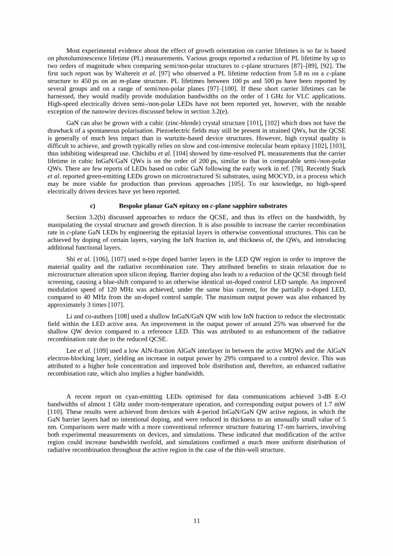
density, as shown in Figure 9.
14
Figure 9: Electrical-to-optical bandwidth versus current density for µLEDs of different diameters, but
from the same 450 nm-emitting 8×8 array. Experimental data reused from [114].
Since capacitance scales with device area this observation indicated that the modulation bandwidth of
these µLEDs was not limited by their RC time constant, as is typically the case for conventional LEDs,
otherwise one would expect to observe that for a given injected current density that the larger µLEDs bandwidth
would be lower than the bandwidth of the smaller µLEDs. This observation that bandwidth varies with current
density is best explained in terms of the modulation bandwidth of these µLEDs being determined by the
differential lifetime of the carriers within their quantum wells (τdiff). The relationship between τdiff and the carrier
density has been extensively studied by others seeking to understand the ‘efficiency droop’ phenomenon that
affects GaN LEDs, where the LED internal quantum efficiency (IQE) decreases as the injected current density
increases. The simple ‘ABC’ model, used to describe carrier lifetimes in semiconductors [115], considers that
the relationship between τdiff and the carrier density (N) is shown by equation (2):
𝜏(𝑁) =
1
𝐴 + 2𝐵𝑁 + 3𝐶𝑁2
(2)
Here A and B are the Shockley-Read-Hall (SRH) non-radiative recombination and radiative
recombination coefficients, respectively. C is a higher-order non-radiative recombination coefficient, attributed
to Auger recombination in other semiconductor materials, although in GaN-based LEDs this remains an ongoing
topic of discussion [82].
From (2) it can be seen that as N increases, τdiff decreases. This provides an explanation for the behaviour
observed in Figure 9 and for the high bandwidths shown by µLEDs in general. Assuming a similar N for similar
current densities, each of the µLEDs in Figure 4 would, therefore, be expected to exhibit a similar modulation
response according to (2). Furthermore, as smaller area µLEDs are able to be driven to higher current densities,
this can explain how they generally exhibit higher modulation bandwidths than their larger area counterparts –
the capability to sustain higher carrier densities allows them to attain higher modulation bandwidth via a
corresponding reduction in τdiff.
High modulation bandwidths from micro-scale LEDs have been reported by several other research
groups. Though there are variations in the structure and fabrication of these devices, high current density
operation underpins the high bandwidths in each case. Liao et al., reported a blue-emitting µLED with a
gallium-doped zinc oxide current-confining aperture [116]. The current-confinement allowed modulation
bandwidth of 225 MHz to be demonstrated. Subsequently, Liao et al. reported current confinement in a green-
emitting µLED by the use of a ring-shaped electrode, with a bandwidth of ~463 MHz reported [27]. Maaskant et
al. reported a 14-element µLED array with a modulation bandwidth > 450 MHz at a current of 70 mA (10
kA/cm2). Inter-connecting 14 elements allowed the output power to be increased, and a data rate of 500 Mb/s
was subsequently demonstrated over a few cm of free space [117]. A cyan µLED with a peak emission of 500
nm and a bandwidth of approximately 400 MHz was reported by Wun et al. [118]. This emission of this 50 µm

15
diameter µLED was optimised for data transmission over polymer optical fibre (POF), and 1.07 Gbit/s data
transmission was demonstrated over 50 m of POF.
These reports demonstrate that very high modulation bandwidths, compared to conventional chip LEDs,
are possible using standard LED epitaxial material and processing techniques, by patterning the LED active area
into µLED structures. High-speed data transmission over free-space and guided wave that has been achieved
with such high bandwidth µLEDs will be discussed in subsequent sections.
f) Plasmonic-enhanced LEDs
A distinct approach to LEDs with high modulation bandwidths exploits resonant interactions between the QW
excitations and surface plasmon polaritons, supported by proximal films or nanostructures of a suitable metal.
Early demonstrations of such effects in III-nitride semiconductors were reported by Okamoto et al., who
emphasized the resonant coupling condition possible between blue-emitting InGaN/GaN QWs and bulk-like
silver [119]. The plasmonic coupling concept has now been applied to III-nitride LEDs quite widely [120], and
recent work has specifically emphasised the potential for VLC. The commonest experimental methodology is to
compare the performance of devices containing metal nanostructures with control devices without these. Zhu et
al. reported on GaN-based plasmonic LEDs which had active areas of 8800 µm2, but in which the epitaxial
wafer was processed into nano-columns down the level of the QW active region, and then re-planarized by use
of a spin-on glass [121]. LEDs in which discrete silver nanoparticles were embedded close to the QWs exhibited
E-O bandwidths of ~30 MHz, approximately twice those of control devices without the silver nanoparticles
present. A different fabrication approach was followed by Yang et al., who exploited the so-called V-pits, of
inverted hexagonal pyramid shape which develop naturally in certain MOCVD growth regimes [122]. Coating
of a heavily V-pitted device surface with silver created a nano-structured metal layer, whose morphology was
shown to be favourable for plasmonic coupling at relatively large separations of >100 nm from the QW active
region. A large plasmonic enhancement in E-O bandwidth was demonstrated for LEDs of 100 µm diameter. At
the highest dc drive voltage of 10 V, a plasmonic-enhanced device had a bandwidth of 200 MHz, versus 115
MHz observed from a counterpart device without the silver layer. Full realization of the potential of plasmonic
effects in high-speed III-nitride LEDs poses various challenges. For example, optimized metal nanostructures
can be designed by finite difference time domain electromagnetic modelling, but can only be approximated by
current fabrication technologies, while practical devices require additional continuous metal layers to spread
current and allow external contacting.
4 High-speed data communication
Optical wireless communication (OWC) for indoor wireless local area networks (WLAN) was first
studied at IBM Laboratory by Gfeller and Bapst in 1979 using infrared radiation [123]. With the development
and wide availability of GaN LEDs in the visible range and due to advantages outlined in section 2, VLC
systems have, however, emerged as the key wireless technology that has the potential to overcome the looming
RF ‘spectrum crunch’ [124]. This section surveys high-speed VLC demonstrations, with a focus on techniques
adopted to improve the data communication capacity of a VLC link.
Table II: Survey of practical demonstrations of VLC systems
Year Sources Modulation
scheme Multiplexing
Pre-
equalisation
Post-
equalisation Data rate (BER threshold) Ref.
2016 RGB LEDs OFDM WDM 10 Gbit/s (BER< 3.8×10⁻³) [18]
2016 µLED PAM Spatial X 7 Gbit/s (BER< 3.8×10⁻³) [33]
2016 µLED OFDM 5 Gbit/s (BER< 3.8×10⁻³) [24]
2016 µLED PAM X 3.5 Gbit/s (BER<3.8×10⁻³) [24]
2016 µLED PAM X 2 Gbit/s (BER< 10-12) [125]
2016 Laser OOK 1 Gbit/s [126]
2015 RGB laser OFDM WDM 12.4Gbit/s (BER< 3.6×10⁻³) [127]
2015 RGB laser OFDM WDM 14 Gbit/s (BER< 3.6×10⁻³) [31]
2015 Blue Laser OFDM 9 Gbi t/s (BER< 3.6×10⁻³) [128]
2015 Blue laser +
phosphor OFDM 5 Gbit/s (BER< 3.8×10⁻³) [43]
2015 Blue laser +
phosphor OFDM Spatial 10 Gbit/s (BER< 3.8×10⁻³) [42]
2015 RYGB CAP WDM X X 8 Gbit/s (BER< 3.8×10⁻³) [34]
2015 RYGB OFDM WDM 5.6 Gbit/s (BER< 3.8×10⁻³) [30],

16
[129]
2015 RGB CAP WDM X 4.5 Gbit/s (BER< 3.8×10⁻³) [130]
2015 Blue laser +
phosphor OFDM 4 Gbit/s (BER< 9.7 ×10⁻⁵) [131]
2015 Blue laser +
phosphor OOK 4 Gbit/s (BER< 3.8×10⁻³) [132]
2015 µLED+ polymer
colour converter OFDM WDM 2.3 Gbit/s (BER< 3.8×10⁻³) [38]
2015 White LED OFDM (bit and
power loading) X 2 Gbit/s (BER< 3.8×10⁻³) [133]
2015 White LED OFDM 1.6 Gbit/s (BER< 3.8×10⁻³) [134]
2015 White LED QAM-OFDM X 1.4 Gbit/s (BER< 3.8×10⁻³) [135],
[136]
2015 White LED PAM X 1.1 Gbit/s [137]
2015 White LED QAM-OFDM X 750 Mbit/s (BER< 3.8×10⁻³) [138]
2015 White LED QAM-OFDM X 682 Mbit/s (BER< 2.5×10⁻³) [139]
2015 LED OFDM Spatial 1.4 Gbit/s (BER< 3.8×10⁻³) [140]
2015 White LED OFDM Spatial 1.3 Gbit/s (BER< 3.8×10⁻³) [141]
2015 Nanowire OOK 1 Gbit/s [113]
2014 16-QAM Polarisation X 1 Gbit/s (BER< 3.8×10⁻³) [142]
2014 Blue LED 4-QAM Spatial X 500 Mbit/s (BER< 3.8×10⁻³) [143]
2014 White LED OOK-NRZ Spatial X 50 Mbit/s (BER< 3.8×10⁻³) [144]
2014 RGB QAM Wavelength 4.22- Gbit/s (BER< 3.8×10-
3) [145]
2014 White LED OOK-NRZ X 340 Mbit/s (BER< 2×10⁻³) [146]
2014 White LED NRZ-OOK X X 550 Mbit/s (BER< 2.6 × 10-
9) [147]
2014 µLED OFDM (bit and
power loading) 3 Gbit/s (BER< 3.8×10⁻³) [25]
2014
µLED+ polymer
colour converter
(white)
OFDM 1.68 Gbit/s (BER< 3.8×10⁻³) [26]
2013 Blue Laser OOK-NRZ 2.5 Gbit/s (BER< 3.8×10⁻³) [148]
2013 Red LED OOK-NRZ 300 Mbit/s (BER< 10-9) [149]
2013 White LED Rate adaptive
OFDM 500 Mbit/s (BER<3.8×10⁻³) [150]
2013 White LED RGB OOK-NRZ Wavelength X 477 Mbit/s (BER<3.8×10⁻³) [151]
2013 White LED OOK-NRZ X 170 Mbit/s (BER<3.8×10⁻³) [152],
[153]
2013 RGB CAP Wavelength X X 3.22 Gbit/s (BER<3×10⁻³) [154],
[155]
2013 µLED (blue) OOK Spatial 1.5 Gbit/s (BER< <1×10⁻¹⁰) [156]
2013 White LED OFDM Spatial 1 Gbit/s (BER<2×10⁻³) [157]
2013 RGB QAM-OFDM Spatial 575 Mbit/s (BER<2×10⁻³) [158]
2012 RGB(WDM) OFDM Spatial 3.4 Gbit/s (BER< 3.8×10⁻³) [159]
2012 RGB OFDM 2.1Gbit/s (BER< 10-3) [160]
2012 White LED CAP X X 1.1Gbit/s (BER< 10-3) [161]
2012 White LED OFDM (bit and
power loading) 1 Gbit/s (BER< 3.8×10⁻³)
[162]
2012 RGB OOK Wavelength X X 614 Mbit/s [163]
2012 RGB DMT-QAM Wavelength 1.25 Gbit/s (BER < 2×10⁻³) [164]
2011 RGB DMT-QAM Wavelength 813 Mbit/s (BER < 2×10⁻³) [165]
2010 µLED (blue) OOK 1 Gbit/s (BER < 1×10⁻¹⁰) [23]
2010 White LEDs DMT-QAM 513 Mbit/s (BER < 2×10⁻³) [166]
2010 White LEDs OOK-NRZ 230 Mbit/s (BER < 2×10⁻³) [167]
2009 White LEDs DMT-QAM 200+ Mbit/s (BER < 10-3) [168]
2009 White LEDs OOK-NRZ 125 Mbit/s [169]
2009 White LEDs OOK-NRZ X 100 Mbit/s (BER < 10-9) [83]
2008 White LEDs OOK-NRZ X 80 Mbit/s (BER < 10-6) [22]
2008 White LEDs OOK-NRZ X 40 Mbit/s (BER < 10-6) [170]
2007 White LEDs DMT-QAM 100 Mbit/s (BER < 10-6) [171]
2006 White LEDs OFDM - [172]
2002 White LEDs BPSK - [173]

17
Figure 10: Progress in the reported data rates using visible GaN LEDs, black (circular) dots representing
demonstration without any multiplexing, red (square) those with spatial multiplexing and blue (triangular) those with WDM.
Table II and Figure 10 clearly demonstrate that the research interest in VLC systems grew significantly
over the last decade. There were few VLC demonstrations using white LEDs before 2008 and reported data
rates were in the range of 100 Mbit/s using analogue equalisation or discrete Multitone (DMT) techniques [22],
[170], [171]. By 2012, Gbit/s systems were demonstrated using a single white LED [161], [162]. More recently,
researchers were able to achieve a 2 Gbit/s link using a commercial white LED [133]. The introduction of
µLEDs for VLC has further fuelled the improvement in the data rate. McKendry et al.showed a 1 Gbit/s free
space VLC link using OOK without any equalisation [23]. Using the optimum bit and power loading DCO-
OFDM, the UP-VLC project demonstrated a 3 Gbit/s link 2013 [25] and more recently a 5 Gbit/s link [24] using
a single blue µLED.
Table I also clearly demonstrates the evolution of the following key technologies that enabled multi-
Gbit/s data rates:
a) Improving the available bandwidth by adopting devices with a higher bandwidth
b) Efficient use of available bandwidth by adopting spectrally efficient multilevel modulations
such as PAM or OFDM
c) Advanced signal processing such as pre-equalization, post-equalization and bit and power
loading (for OFDM)
d) Exploiting the spatial dimension using spatial diversity and/or multiplexing
e) Exploiting the colour dimension using WDM
These key technologies that have enabled multi-Gbit/s VLC systems are discussed in the following sections.
4.1 Modulation schemes
The coherent transmission that has served well for RF communications is not cost-effective for VLC
systems [48]. The low-cost VLC (and OWC in general) systems use optical intensity modulation (IM) and a
direct detection (DD) receiver (referred to as IM/DD), i.e. information is modulated in the instantaneous
intensity of an optical carrier, and the receiver detects the optical intensity of the incoming signal [48]. As a
result, there are fundamental differences between RF and optical communications: a) information in OWC is
carried on the intensity of an optical carrier, contrary to the amplitude and phase of the RF carrier, and the
receiver detects the optical intensity of the incoming signal, b) optical signals are real-valued and unipolar
whereas RF signals can be complex-valued and bipolar, and c) the signal-to-noise ratio (SNR) is proportional to
the square of the received optical power, rather than the square of the carrier amplitude in the case of RF. As a
result, only the baseband transmission is cost-effective for VLC systems i.e. there is no up-conversion to the
carrier frequency using a local oscillator. Moreover, bipolar signalling schemes must be biased with a DC level
18
to make them unipolar. Consequently, the modulation schemes employed in RF systems may need to be
modified when applying them to VLC systems, which results in reduced spectral and power efficiencies [174].
Selecting a modulation technique depends on a number of key criteria. The important criteria that are
often used as benchmarks for comparison of modulation schemes are listed below:
a. Power Efficiency: Power efficiency is the most important criterion when evaluating modulation
techniques. The electrical power efficiency ηp is the average electrical power required to achieve a
given error probability at a given data rate and is defined as [48], [175]:
𝜂𝑝 =
𝐸𝑝𝑢𝑙𝑠𝑒
𝐸𝑏
(3)
where 𝐸𝑝𝑢𝑙𝑠𝑒 is the energy per pulse and Eb is the average energy per bit.
b. Bandwidth Efficiency: Bandwidth efficiency, also refer to as spectral efficiency, determines the
number of bits that can be assigned per unit available bandwidth (i.e. bits/s/Hz) and is defined as:
η𝐵 =
𝑅𝑏
𝐵
(4)
where Rb is the achievable bit rate and B is the bandwidth of the system.
c. Receiver sensitivity: The receiver sensitivity is defined as the minimum optical power required to
achieve a desirable error probability. The receiver sensitivity is related to power efficiency. The
ratio of electrical power to optical power is dependent on the absolute level of optical power [176]
and modulation schemes. Note that the smaller the receiver sensitivity, the better is the system, as
such a system requires less power to achieve the desirable error probability.
The modulation schemes for VLC systems may be classified into a) baseband modulation and b)
subcarrier modulation (SCM). The popular baseband modulation schemes include on-off keying (OOK), pulse
amplitude modulation (PAM), pulse position modulation (PPM) and pulse interval modulation (PIM). The
subcarrier base modulation includes orthogonal frequency division multiplexing (OFDM) and carrier-less
amplitude and phase (CAP) modulation. There are other forms of modulation known as colour shift keying
(CSK), which are based on constellation mapping by varying the colour space in the chromaticity diagram [19],
[177]. However, the high-speed practical VLC demonstrations are geared towards the use of OOK, PAM,
OFDM, and CAP. An overview of these modulation schemes is given in the following sub-sections.
a) On-off keying (OOK)
OOK is the simplest form of baseband modulation for IM/DD where information is sent by switching a
source ‘ON’ and ‘OFF’ at a rapid speed. In the OOK non-return-to-zero (OOK-NRZ) scheme, ‘ones’ and
‘zeros’ are represented by the presence or absence, respectively, of an optical pulse for the bit duration, as
illustrated in the time waveforms in Figure 11(a) . The popularity of OOK is due to its simplicity in
implementation and power efficiency. For example, a digital switching circuit like a NAND gate can serve as
the driver for switching the light sources ‘ON’ and ‘OFF’ [45] and a simple digital comparator at the receiver
can recover the binary data. Because of the simple driver circuit requirement, it is easy to fabricate integrated
driver circuits that can drive a large number of LEDs independently. McKendry et al. demonstrated a
Complimentary Metal-Oxide-Semiconductor (CMOS) based driver for GaN LED that can individually and
independently control a 16×16 array of µLEDs [23]. OOK-NRZ has been widely adopted for VLC, see Table 1.
Le Minh et al.adapted an OOK-NRZ scheme with pre/post equalisation and demonstrated up to 100 Mbit/s
using commercial white LEDs [22], [83], [170]. Vuvic et al.demonstrated data rates up to 230 Mbits/s at 1000
lux [167]. Fujimoto et al. used a pre-emphasis circuit with OOK-NRZ to achieve a data rate of 477 Mbits/s
using a red LED [151] and 614 Mbits/s by adopting analogue pre- and post-equalisation circuits [163]. Using a
commercial phosphor-based white LEDs, Li et al.demonstrated 550 Mbit/s real-time VLC [147]. Using high
bandwidth µLEDs, up to 1.7 Gbits/s single-channel VLC links were recently demonstrated [23], [24], [156].
b) Pulse Amplitude Modulation (PAM)
In an L-PAM scheme (where typically L=2M and M is a positive integer), a pulse is selected from the
alphabets of {0, 1, 2, … , (𝐿 − 1)} to represent an M-bits input symbol. The spectral efficiency of multi-level
PAM increases linearly with the bit resolution, but at the cost of reduced power efficiency [178], [179]. In
addition to the optical power penalty due to multi-level signalling, multi-level PAM further suffers from optical
power penalty due to the LED non-linearity. Hence, it was experimentally demonstrated that 4-PAM (Figure

19
11(b)) offers improved performance in comparison to higher level PAM even in severely band-limited systems
[125], [180].
Yang et al. [181] introduced differential PAM for bandlimited VLC systems. In the diff erential PAM
scheme, signals with equal amplitudes but a unit time delay are transmitted through diff erent LEDs. Optical
signals from these LEDs are superimposed in free space and detected using a single optical receiver. A 100
Mbits/s link was demonstrated with differential PAM using white LEDs. Li et al.demonstrated that it is feasible
to generate multi-level PAM by linearly combining optical intensity in free space from spatially separated
multiple LEDs [182]. This superposed PAM (SPAM) is insensitive to the non-linearity of the individual LEDs.
c) Pulse position modulation (PPM)
PPM (Figure 11(c)) is an orthogonal modulation scheme where information is carried in the position of a
pulse within the symbol period. Each PPM symbol consists of L time slots. Within the PPM symbol, all slots
except one are empty and the temporal position of this pulse within the symbol period carries the information.
Hence, PPM requires both slot and symbol synchronization at the receiver and is therefore vulnerable to loss of
synchronization. However, PPM is well known for its power efficiency and has a long legacy of application in
fibre optics and space communications [183], [184].
Most of the VLC systems have a high SNR, but limited bandwidth due to the use of phosphor-containing
LEDs [185]. Because of the poor spectral efficiency of PPM, there is a limited adoption of PPM for high-speed
VLC systems. Nonetheless, PPM is adopted in the IEEE 802.15.7 standard and the IrDA serial data
communication standard [19]. IEEE 802.15.7 recommend a variable PPM, which changes the duty cycle to
achieve a required dimming level [19]. There are also a number of variations to standard PPM including
differential PPM (DPPM), overlapping PPM (OPPM) multiple PPM (MPPM), and expurgated PPM (EPPM).
The study of these modulation schemes is not within the scope of this review. The interested reader can refer to
references [186]–[189].
Figure 11: Time waveforms of (a) OOK, (b) 4-PAM, and (c) 4-PPM for a binary input sequence of {110100100011}
for the same data rate
d) Carrier-less amplitude and phase modulation
CAP bears a similarity to quadrature amplitude modulation (QAM), as both schemes use orthogonal bases to
transmit two data streams in parallel. Unlike QAM, however, CAP does not use sinusoidal carriers to generate
orthogonal components. Instead, CAP uses a pair of digital filters whose impulse response forms a Hilbert
transform pair used as the orthogonal bases. Hence, the CAP is generated by combining two PAM signals which
are convolved with these filters. If the two filters are chosen as sine and a cosine, then CAP offers identical
performance to QAM [190]. The key advantages of CAP over QAM, however, is a simpler implementation
Time
Am
pli
tud
e
OO
K4
-PA
M4-P
PM
(a)
(b)
(c)

20
[190] as it is not necessary to modulate the baseband CAP signal with quadrature carriers. This makes CAP an
attractive scheme for IM/DD systems.
The impulse responses of the two orthogonal filters can be calculated using time-domain multiplication
of cosine and sine with a root-raised cosine filter (RRCF) for in-phase (I) and quadrature phase (Q) channels,
respectively. Figure 12 (a) and (b) show the transmitter pulse shaping filters for I and Q channels along with
cosine and sine and root-raised cosine filter (RRCF) impulse response. Three parameters determine the impulse
response of the transmitter filters: the sine and cosine frequency, the RRCF roll off factor α and the filter length
(i.e. number of filter taps) [191]. The frequency can be arbitrarily chosen as long as it is higher than the highest
frequency of the SRRC. The roll-off factor α determines the minimum bandwidth requirement and the filter
length. The minimum passband bandwidth requirement for a CAP signal is Rs(1 + α) where Rs is the baud rate
and 0 ≤ 𝛼 ≤ 1. This means efficient use of available bandwidth can be achieved by choosing the value α close
to zero. This, however, increases the complexity as a larger number of taps are required to meet the roll-off
factor [191]. The smaller roll-off factor also increases the peak-to-average-power-ratio (PAPR) [192] which is
potentially an issue for a limited dynamic range system.
(a)
(b)
(c)
Figure 12: a) transmitter filter for I-channel, b) transmitter filter for Q-channel and c) the schematic block
diagram of the CAP signal generation and demodulation.
QA
M m
app
ing
Up
-sam
pli
ng In-phase
shaping filter
Quadrature
shaping filter
DACInput
Bit stream
DC-bias
Transmitter
Dem
app
ing
dow
n-s
ampli
ng In-phase
matched filter
Quadrature
matched filter
ADC Receiver
Eq
ual
izat
ion
Output
Bit stream

21
A schematic block diagram of CAP signals generation and demodulation given in Figure 12 (c). Notice
that the CAP modulator and demodulator resembles the traditional QAM system except that the multiplier
(multiplying input signal with a carrier signal) is replaced by a bandpass filter [193]. When the carrier frequency
is not high, the filters (given in Figure 12 (a) and (b)) can be approximated with a reasonable number of taps.
For a high carrier frequency, it is not feasible to approximate the filters [193]. This is the reason CAP is popular
for the baseband transmission system [161].
CAP is generated by first mapping the incoming bit stream into a complex QAM constellation, which is
then up-sampled by a factor of Ns, the number of samples per symbol, by inserting Ns-1 zeros between two
symbols. The I and Q sequences are separated and the pulse shaping filters are applied. The outputs of the filers
are then summed and converted to analogue signal by an analogue-to-digital converter (ADC). Since CAP
signals are bipolar, a DC-bias is added before intensity modulation of the optical transmitter. At the receiver
end, two matched filters (matched to I and Q transmitter filters) separate the two orthogonal signals. Then down-
sampling and signal recovery is carried out, which involves equalization and de-mapping [194].
CAP offers a simpler implementation with much lower PAPR than OFDM [155]. However, for optimum
performance, CAP requires a flat-band response. For non-flat spectral systems, CAP requires very complex
equalizers [34], [195]. Recently, a multiband CAP was proposed which divides the bandwidth into a number of
sub-bands [155]. With a sufficiently large number of sub-bands, each sub-band can be considered to be flat
relaxing the condition for a flat-band response. The number of bits/symbol assigned each sub-band can be
adjusted as in the case of the bit and power loading OFDM scheme [191], [196], [197]. Multi-band CAP,
however, suffers from high PAPR as in the case of other subcarrier modulation [197].
e) Orthogonal frequency division multiplexing (OFDM)
OFDM is a special case of subcarrier modulation in which the carriers are orthogonal over one symbol
period. Since data are transmitted in parallel over a relatively large number of subcarriers, the symbol period for
each subcarrier is much longer than for a serial system and, hence, ISI is significantly reduced [174], [172].
Each subcarrier in OFDM is independently modulated and can adapt to match the system frequency response.
Hence, OFDM is a preferred option in a band-limited system. Another key advantage of OFDM is its simplicity
in implementation as an Inverse Fast Fourier Transform (IFFT) and Fast Fourier Transform (FFT) pair can be
used to generate and demodulate the OFDM signal (see Figure 13).
Figure 13: A schematic block diagram of the DCO-OFDM signal generation and demodulation.
Conventional OFDM cannot be directly applied to the IM optical system because the OFDM signals at
the output of IFFT (Figure 13) are complex and bipolar and an IM/DD system requires a real and unipolar signal
[174]. In order to generate a real signal, Hermitian symmetry is imposed before applying the IFFT i.e. the
subcarriers corresponding to the negative frequencies are made complex conjugates of the other half [174]. This
reduces the spectral efficiency at least by a factor of two in comparison to conventional OFDM [198], [199].
The real signal is further conditioned to generate a unipolar signal as described below.
In a DC-biased optical OFDM (DCO-OFDM), a Hermitian symmetry is imposed before applying the
IFFT to generate a real signal. The output of the IFFT is hard-clipped and a DC-bias is applied to make the
signal unipolar. Figure 13 shows the block diagram of DCO-OFDM generation and demodulation processes.
QA
M m
app
ing
and
S
/P
Her
mit
ian
sym
met
ry
Bit stream
DC-bias
Transmitter
1-t
ap e
qual
iser
Rem
ove
CP
and S
/P
ReceiverFF
T
Output
Bit stream
IFF
T
P/S
+ C
P
Cli
ppin
g, D
AC
,
and f
ilte
r
Fil
ter
and A
DC
Dec
odin
g a
nd
P/s

22
First, input bit streams are mapped to QAM constellations followed by a serial to parallel (S/P) converter. The
signal is then mapped to orthogonal subcarrier frequencies by IFFT. Note that signal on the second half of IFFT
inputs is the complex conjugate of the first half, in order to generate real outputs. In most practical OFDM
systems, a cyclic prefix (CP) is added to the start of each OFDM symbol i.e. a number of samples from the end
of the symbol is appended to the start of the symbol. Though the CP introduces reduces the overall throughput,
it eliminates both ISI and inter-carrier interference (ICI). The OFDM symbols are then serialized using P/S,
followed by conversion to analogue signals using a digital-to-analogue converter (DAC) and a filter. An
appropriate clipping is applied before DC addition to make the signal unipolar. One of the key issues with
OFDM signals is their high PAPR [200] and, hence, the OFDM signal needs to be clipped significantly in a
dynamic-range-limited system. Even with a high DC-bias, a portion of the negative signal is clipped, thus
limiting the performance.
The signal recovery process almost follows the inverse of signal generation. First, the received signal is
converted to a discrete time signal by filtering and an analogue-to-digital converter (ADC) followed by CP
removal and serial-to-parallel (S/P) conversion. Then, a FFT is applied to the signal followed by 1-tap frequency
domain equalization, parallel-to-serial (P/S) conversion and finally the symbol recovery.
In asymmetrically clipped optical OFDM (ACO-OFDM), the signal is clipped at zero level [201] and
hence does not require an additional DC-bias. This is achieved by assigning QAM symbols only to odd
subcarriers. In this case, noise generated by asymmetrical clipping below the zero level only falls into even
subcarriers, and odd subcarriers are not impaired [201]. Thus, by giving up half of the spectrum, ACO-OFDM
reduces the need for a DC-bias. This in return improves the optical power efficiency, but at the cost of reduced
spectral efficiency.
Further modifications have been proposed to make OFDM more suitable for IM. Unipolar OFDM (U-
OFDM) [202] and flip-OFDM [203] separate the positive and negative signal of the IFFT output into two
separate frames. The polarity of negative amplitudes is inverted to make them unipolar and zeros are padded
before or after each sample to differentiate positive and negative samples. U-OFDM and flip-OFDM offer the
same spectral efficiency as ACO-OFDM and achieve the same performance in an additive white Gaussian noise
(AWGN) channel [204]. Further improvement in spectral efficiencies can be achieved by superimposing
different layers of U-OFDM as outlined in [202].
Azhar et al.[205] performed an experimental comparison of different OFDM schemes. It was concluded
that in practical systems with a limited dynamic range, DCO-OFDM outperforms other OFDM schemes. The
inferior performance of ACO-OFDM was among other things primarily attributed to the introduction of baseline
wander (BLW) due to clipping at zero level. A similar conclusion was obtained analytically in [206], where it is
shown that DCO-OFDM outperforms flip-OFDM in an average optical power and dynamic range limited
system.
4.2 Comparison of Modulation schemes
The selection of an appropriate modulation scheme depends on a number of factors, most importantly
spectral efficiency, power efficiency, complexity, reliability, robustness towards interference and resilience to
system non-linearity. Due to a number of non-mutual parameters that affect the optimum performance, it is not
straightforward to compare modulation schemes under diverse system constraints. Hence, a general conclusion
is difficult to draw and contradictory results may be obtained depending upon the underlying assumptions. This
section surveys the performance comparison of different modulation schemes, exclusively based on
experimental results. Note that these results need to be interpreted with a caution, as they may not match
theoretical predictions due to the difference in the underlying assumptions. For example, most of the theoretical
studies are carried in an ideal AWGN without a dynamic range limitation and a nonlinear distortion, thus
favouring some modulation schemes that may not be optimal in practice.
The optical power penalties for multi-level PAM schemes with a decision feedback equaliser (DFE)
depend on the ratio of bandwidth to the data rate. Theoretical studies [178] showed that OOK requires a lower
optical power than multi-level PAM if the data rate is less than three times the bandwidth. If the LED is
modulated beyond three times the bandwidth, multi-level PAM performs better than OOK. The performance of
multi-level PAM schemes, however, degrades in the presence of system non-linearity and hence most of the
practical work tends to concentrate on a maximum PAM level of L=16. The simulation and experimental studies
carried out by Li et al. showed that 4-PAM offered the best receiver sensitivity in comparison to 2-PAM and 8-
PAM [125] i.e. 4-PAM requires the lowest received optical power to achieve the desirable error rate. Similar
conclusions were reached for MIMO-VLC systems [207] and for high-speed polymer optical fibre applications
as well [180].

23
Among the huge number of variations of OFDM that have been applied to VLC, ACO-OFDM, PAM-
DMT, flip-OFDM, U-OFDM and enhanced U-OFDM offer equivalent spectral efficiencies and performance in
an AWGN channel [204]. ACO-OFDM offers higher power efficiency than DCO-OFDM for an AWGN
channel. However, in a severely bandwidth-limited system, ACO-OFDM is disadvantageous as it wastes half of
the spectrum. Similarly, in a dynamic range limited system, the ACO-OFDM signal needs to be clipped at the
upper level as well. Unlike zero level clipping, the noise generated by upper-level clipping falls in both the odd
and even subcarriers. Similarly, system non-linearity generates harmonics which again affect both the even and
odd subcarriers. These effects will degrade the performance of ACO-OFDM. Moreover, the spectrum of ACO-
OFDM has a large DC component [176] and in an AC-coupled system, this will cause significant baseline
wander. Considering all these issues that arise in a practical system, it is not unanticipated that DCO-OFDM
outperforms other OFDM schemes in a bandwidth and dynamic-range limited VLC system [37], [205], [206].
However, by using pre-equalization and using twice the bandwidth of DCO-OFDM, it was shown in [208] that
ACO-OFDM required 1.5 dB less optical power than DCO-OFDM to achieve same data rate.
PAM, CAP and OFDM depend on the non-linearity, dynamic range, available SNR, and on the ratio of
bandwidth to the data rate. At the high bandwidth to data rate ratio (i.e. low ISI), PAM schemes tend to offer the
best performance, whereas at a low ratio (i.e. high ISI), OFDM tends to offer the best performance [178], [209].
A performance evaluation of OFDM and PAM is carried out in [210] for an intensity modulated optical
communications system. The authors have considered nonlinear distortion caused by signal clipping and the
limited resolution of the digital-to-analogue converter. Based on the analytical results, and confirmed by Monte
Carlo simulations, the paper concluded that PAM modulation schemes outperform OFDM and require 3 – 3.5
dB less optical power for bit resolutions of less than four. The experimental results demonstrated in [180] also
highlighted that PAM outperforms OFDM. Stepniak et al. carried out theoretical comparisons of a number of
modulation schemes for an indoor VLC system in [211] and studied these experimentally in [212]. The
theoretical investigation in [211] indicates that among PAM with DFE, CAP with DFE and DMT with bit and
power loading, PAM with DFE offers the best performance. Similar conclusions were reached when the
comparisons of these modulation schemes were carried out experimentally for a VLC system with a white LED
[212]. It has also been shown that 2-PAM and 4-CAP exhibit improved immunity to nonlinear distortions
compared to their higher level counterparts. Note that the comparison of these modulation schemes was carried
out at modest data rates of 300 Mbit/s and 450 Mbits/s, which is significantly lower than the maximum data
rates demonstrated using white LEDs. The performance of OFDM and CAP was also assessed in [155] using a
single colour LED as well as a WDM system with RGB LEDs. In this work, an optimal bit and power loading
technique was adopted for OFDM, and pre-emphasis and post equalization was adopted for the CAP. The
maximum data rates achieved using CAP for both single and multi-colour systems were higher than those
obtained with OFDM. These studies clearly indicate that, unlike in RF, OFDM is not always the optimum
modulation scheme for IM optical communication. Nonetheless, most of the world record data rates for VLC
systems have been achieved using a single colour or RGB LEDs with bit and power loading OFDM [18], [25],
[30], [133].
4.3 Equalization techniques
Most VLC links are intrinsically line-of-sight (LOS). LOS link channels generally have high bandwidth
in excess of GHz. However, the transceiver elements (especially white LEDs) impose a significant bandwidth
bottleneck for high-speed communications, because (as discussed above) commercial white LEDs have a
bandwidth of only a few MHz and the blue LED itself has a limited bandwidth of 10’s of MHz. Though recently
introduced GaN µLEDs have a larger bandwidth up to 100’s of MHz (as described in Section 3) [23], this is still
only a fraction of the targeted data rate in the Gbit/s range. Hence, a number of techniques have been devised
and studied to mitigate limitations of the modulation bandwidth. Equalization is a key technology to increase the
effective bandwidth by applying a filter that has a frequency response inverse to the system response.
Equalization can be analogue or use discretized time, and it can be applied in VLC systems either at the
transmitter (pre-equalisation) or at the receiver (post-equalisation). These equalization techniques are discussed
in the following sections.
a) Analogue equalization
The frequency response of an LED can be modelled using a first order low pass filter (LPF) [83] i.e.
there is a 20 dB/decade increment in the attenuation for the frequencies above the 3 dB bandwidth. This rapid
fall-off in the response can be compensated by the introduction of an analogue filter bank, with a combined
response which is the inverse of the LED response. One of the simplest techniques to compensate the roll-off is
using passive RC high-pass filters with different cut-on frequencies and applying weighted summing to the
output of the filters [170]. Figure 14 showed an illustration bandwidth improvement using a simple analogue
pre-equalization. Using a simple passive RC pre-emphasis, Burton et al.achieved an overall system bandwidth

24
of 10 MHz for a white phosphor LED [213]. Le Minh et al. achieved a tenfold increment in the bandwidth, from
~ 2.5 MHz to 25 MHz, by applying analogue resonant circuits with different central frequencies to 16
independent LEDs and combining their outputs. By using a similar technique, a bandwidth of 45 MHz was
achieved for the filtered blue response and an 80 Mb/s short range data link has been demonstrated [22].
Figure 14: Frequency responses of a typical LED without and with an analogue pre-equalization. There is
a more than fourfold increase in the equalized bandwidth.
Using active components, Li et al. demonstrated an analogue pre-emphasis circuit which extended the
blue spectrum -3 dB bandwidth from 12 to 77 MHz [214]. They further improved the bandwidth up to 233 MHz
using multi-stage pre-emphasis based on NPN transistors, enabling data transmission of 550 Mb/s using OOK-
NRZ [147], [215] and 682 Mb/s using 16-QAM-OFDM [139]. Fujimoto et al. proposed a practical LED driver
with a pre-emphasis circuit based on a current mode logic (CML) circuit, emitter follower, and RC network and
demonstrated a data rate of 662 Mb/s using a blue LED [151], [163], [216]. Kishi et al. demonstrated an LED
driver that sweeps out the remaining carriers in the LED when the LED is going into an off-state [217]. Pre-
distortions are also adopted for other modulation schemes including CAP and OFDM [34], [133], [134], [136],
[138], [218].
For VLC applications, post-equalization (equalizer at the receiver) is often the preferred option, although,
for a linear system, similar performance can be achieved by pre- and post-equalization. If the primary role of the
visible LEDs is to provide illumination then high current driver circuits need to be used to provide adequate
illumination. If pre-equalization is adapted, the equalizer needs to be designed such that it can withstand a
current of hundreds of milliamps, which is very challenging. If multiple sources are used to provide a high level
of illumination or coverage, modification needs to be made for each individual source, thus making the system
expensive. The limited dynamic range and non-linearity of the sources also need to be taken into account for
optimum equalization. Moreover, the pre-equalizers (based on RC high pass filter) suppress low-frequency
components leading to a lower modulation depth and reduced SNR. Post-equalizers are free from these
constraints. However, post-equalization enhances noise and pre-equalization can offer a better receiver
sensitivity [125].
Using an RC-network based on a first-order analogue post equalizer, Le Minh et al.improved the LED
bandwidth from 14 MHz to 50 MHz and achieved a 100 Mb/s link using OOK-NRZ modulation schemes [83].
Using a post-equaliser based on two passive and one active equaliser, Li et al.extended the LED bandwidth by
more than 50 times the raw bandwidth and demonstrated a 340 Mb/s VLC link [146]. Simple RC-based post
equalizers were investigated for a number of modulation schemes in [182], [219], [220]. The pre- and post-
analogue equalizations were combined to further improve the data rate beyond 500 Mb/s [147], [216].
b) Discrete-time equalization
Discrete-time equalization is typically preferred over analogue equalization as the former offers
improved performance [221] and it can be implemented in any modern digital signal processing (DSP) platform,
making it easy to adapt to specific applications. Since the ISI caused by limited bandwidth system response is
limited to a finite number of symbols, the discrete-time equalizer can be realized based on a finite impulse
response (FIR) digital filter. If a system is time-invariant and the response is known in advance, the filter
coefficients can be predefined. In a time-variant system, the filter coefficients are adjusted dynamically by
transmitting a training sequence in a regular interval.
Discrete-time equalizations are classified into either linear equalizers or decision feedback equalizers
(DFEs). A linear equalizer is constructed with a transversal filter that contains delay taps and weighting

25
coefficients (Cn) on each tap (see Figure 15(a)). For zero ISI at the sampling instant, the frequency response
Ge(f) of the equalizer should be an inverse of the system impulse response c(f) [222] i.e.
𝐆𝑒(𝒇) =
𝟏
𝐂(𝒇).
(5)
This class of filter is called the zero forcing equalizer (ZFE) as the ISI is zero at the sampling instant. A
major drawback of the ZFE is that it ignores the presence of additive noise. This results in a significant noise
enhancement. An alternative is the minimum mean-square error (MMSE) criterion which relaxes the zero ISI
condition. The MMSE concurrently minimizes the ISI and noise, giving an optimum performance in the
presence of AWGN.
A decision-feedback structure completely removes ISI caused by the previously detected symbols by
feeding them back using a feedback structure (see Figure 15(b)). If the current symbol is detected correctly, then
the ISI contributed by this symbol in the future received signal can be accurately predicted and removed. The
DFE offers significantly improved performance in comparison to ZFE, especially for a severely band-limited
system [178]. In fact, the performance of the DFE is close to that of the optimal maximum likelihood sequence
detection (MLSD) technique [223].
As in the case of analogue equalization, both pre- and post-equalizations have been studied for VLC
applications. Li et al. [125] investigated discrete-time feed-forward pre- and post-equalizations with various
numbers of filter taps for PAM schemes. The simulation results showed that the pre-equalization outperforms
post-equalization and an improvement of up to 5.5 dB in receiver sensitivity was obtained for OOK-NRZ. An
error-free 2 Gb/s VLC link was also demonstrated using a µLED and APD receiver. By adaptively changing the
pre-equalizer filter coefficients, Yeh et al. improved the system bandwidth using a linear pre-equalizer and
achieved 20 Mb/s using an LED with a bandwidth of 1 MHz [224]. Haigh et al. applied an adaptive linear
equalizer and demonstrated a VLC link with a data rate of above 100 Mb/s using the blue spectral component of
a white LED with a bandwidth of 8 MHz [225].
(a)
(b)
Figure 15: Schematic of time-domain a) linear equalizer and b) decision feedback equalizer.
A theoretical study showed that DFE significantly outperforms a linear structure without significantly
higher complexity [178], which was verified practically in [153]. As a result, most of the high speed VLC
Z-1
× × ×
yi
C0 C1 CN-1
∑
Z-1 Z-1. . .
Z-1
× × ×
yi
C0 C1 CN-1
∑
Z-1 Z-1. . .
Z-1
× × ×
BMB1 B0
Z-1 Z-1. . .

26
demonstrations to date use DFE [137], [153], [155], [161], [226] often in combination with analogue pre-
equalization [34], [155]. A fractionally spaced blind DFE algorithm was investigated in [227] in combination
with OOK-NRZ and demonstrated a 10 Mb/s link using an LED with 1 MHz bandwidth. DFE was also
successfully applied to CAP to demonstrate a multi-Gb/s VLC link [154], [161]. A complex DFE is adopted in
these reports and is applied to the in-phase and quadrature-phase channels of CAP.
Typically, LEDs have non-linear impulse responses. FIR-filter-based equalizers are not optimal for the
compensation of ISI in a non-linear system [228], [229]. Rajbhandari et al. studied an artificial neural network
(ANN) based receiver for compensating ISI and non-linear response of VLC systems and practically
demonstrated that the ANN outperforms filter-based equalizers [152], [153]. For example, a data rate of
170 Mb/s was achieved using a decision feedback ANN structure for OOK-NRZ. For the identical link, only
90 Mb/s was feasible with DFE, demonstrating a clear advantage of ANN for the VLC link. However, the
computational complexity of the ANN-based receiver is significantly higher than DFE, as the ANN employs
non-linear transfer functions to realize a non-linear response. Alternatively, a Volterra-based nonlinear DFE was
adapted to compensate the LED non-linearity and ISI for PAM and CAP modulation schemes [34], [130], [137],
[230]. In [230], a non-linear DFE structure was realized with a second order nonlinear Volterra feed-forward
section. It was demonstrated that the Volterra DFE can efficiently compensate LED nonlinearity and can
improve the receiver sensitivity by up to 5 dB for multilevel PAM. A data rate of 1.1 Gb/s was accomplished
using the symbol-spaced Volterra DFE for the PAM scheme [137]. Due to the non-linear response, the Volterra
DFE requires a significantly longer training time as the convergence is slower than in the case of traditional
DFE [230]. In order to reduce the training duration, Wang et al. proposed a modified cascaded multi-modulus
algorithm (M-CMMA) which updates the filter weights of the nonlinear equalizer without using training
symbols [130]. An aggregate data rate of 4.5 Gb/s was achieved with RGB LEDs by compensating the non-
linearity with the Volterra DFE using M-CMMA training. They further improved the data rate up to 8 Gb/s
using a hybrid equalizer consisting of a linear, a Volterra-series-based nonlinear, and a decision-directed least
mean squares equalizer [34]. Non-linear compensation techniques using pre-distortion and post-distortion are
further outlined in [231]–[233].
Frequency domain equalizers (FDE) have recently also been explored for VLC systems [143], [145],
[234]–[237]. In the FDE approach, a fast-Fourier-transform (FFT) is performed on a block of symbols before
applying a single-tap equalizer in the frequency domain as in the case of the OFDM. The combination of PAM
with block transmission and FDE has potential to offer improved performance over PAM-DMT and OFDM
[237], [238]. Kashani et al. studied the performance of Nyquist single carrier FDE (NS-CFDE) for VLC [239].
The NS-CFDE has a similar spectral efficiency as DCO-OFDM but a significantly reduced PAPR. Hence, NS-
CFDE has potential to outperform OFDM and OOK schemes, especially for dynamic range limited cases [239].
Wang et al. applied NS-CFDE [145] experimentally and demonstrated a data rate of 4.22-Gb/s for RGB LEDs
with WDM. NS-CFDE was also studied for a 2×2 MIMO system [143] where MIMO de-multiplexing and post-
equalisation were employed in the frequency domain.
The OFDM scheme uses a single tap FDE to compensate for ISI. OFDM-VLC demonstrations often
apply an analogue pre-equalization and frequency domain post-equalization [134], [138]. Xingxing et al. [130]
applied a cascaded analogue pre-equalizer to increase the −3 dB bandwidth of commercial white LEDs from 17
MHz to 366 MHz, and a data rate of 1.6 Gb/s was demonstrated using 16-QAM-OFDM. In [25], the
performance of DCO-OFDM with pre-equalization and post-equalization was investigated for a blue µLED and
it was demonstrated that combining pre- and post- equalizations offers an improved performance rather than
relying only on the post-equalization. The optimum performance, however, was obtained by applying an
adaptive bit and power loading [25]. In sub-carrier modulation schemes like OFDM, the constellation level and
the assigned power level in each sub-carrier can be independently adjusted depending upon the available SNR,
thus optimizing the achievable data rates. Using adaptive bit and power loading, a blue µLED based VLC link
achieved 3.22 Gb/s in comparison to 2.63 Gb/s using combined pre- and post-equalization [25]. Similarly, for a
VLC link based on a single phosphorescent white LED with a blue filter, a data rate of 2 Gb/s was achieved
using adaptive bit and power loading in [133] whereas the same link offered only 1.6 Gb/s when incorporating
analogue pre-equalization with post equalization. These results clearly demonstrated that OFDM with bit and
power loading maximize the system capacity and, as a result, most of the high-speed VLC demonstrations have
employed adaptive bit and power loading [18], [25], [30], [159], [240]. The performance of OFDM also suffers
due to its high PAPR and susceptibility to a nonlinear system response. The effect of non-linearity can be
reduced by limiting the PAPR by pre/post distortion. In [200], the authors recommended applying an inverse
nonlinear polynomial of the LED I-V response to a signal before intensity modulating the LED so that the
overall system response is a linear function. A hybrid time-frequency domain equalization that compensates ISI
and nonlinear distortion for OFDM was experimentally demonstrated in [240]. In this case, ISI was
compensated by FDE and the nonlinear distortion by an adaptive nonlinear-Volterra-based time domain

27
equalizer. Qian et al. proposed an adaptive post-distortion for compensating the non-linear response of LEDs
[232]. The authors applied a memory polynomial model to track and compensate the LED’s nonlinearity.
4.4 Spatial Multiplexing/Modulation
VLC systems can take advantage of the availability of multi-element, multi-coloured illumination
devices to improve coverage, data rate and the reliability of the communications system by exploiting spatial
multiplexing and WDM. This section provides an overview of spatial modulation/multiplexing and WDM is
introduced in the next section.
There are a number of ways to drive the spatially separated LEDs required, which can be broadly
classified into:
a) A ‘ganging’ approach
b) A multiple input multiple output (MIMO) approach
a) Ganging Approach
In the ganging approach, also known as repetition coding [241], multiple LEDs are modulated using the
same data source and spatially superposed as shown in Figure 16. The individual LEDs can have an individual
driver with all drivers receiving the same data. Alternatively, the LEDs can be connected in series or parallel
and driven by a single driver. Multiple LEDs are ganged together in order to provide a better link margin, wider
coverage or increased resilience to blocking of the path between LED and receiver. In [170], 16 white LEDs
were driven by 16 drivers to provide an improved SNR at the receiver and a data rate of 40 Mb/s was achieved
using OOK-NRZ. In [242]–[244], increased area coverages were achieved using a number of transmitters each
of which had a limited divergence angle and pointed in a different direction. Increased angular diversity can be
achieved by a planar array of LEDs in combination with optics as in [244] or by arranging LEDs in a semi-
spherical base with each LED pointing in a different direction [242], [243].
(a)
(b)
Figure 16: Approaches to drive multiple LEDs using an individual driver a) ganging approach and b) MIMO
approach.
dataCombining
and post
processing
LED
driver 1
data
LED1
LED
driver 2
LED2
LED
driver M
LED M
Optics
Amplifier
PD1
Amplifier
PD2
Amplifier
PD N
data1 LED driver 1
LED1
data2 LED driver 2
LED2
data M LED driver M
LED M
Amplifier 1
PD1
Amplifier 2
PD2
Amplifier N
PD N MIM
O d
eco
der
data1
data2
data M
Imag
ing
Op
tics
28
The spatial diversity can be applied to the receiver by different diversity combing algorithms which
include equal gain combining (EGC), maximum ratio combining (MRC) and selection combining (SelC). In the
EGC spatial diversity technique, the photocurrents from all receivers are summed giving equal weight to them.
In the MRC techniques, a weight proportional to the received optical power is given to each receiver before
linearly combining the photocurrent. In the SelC algorithm, the receiver with the highest SNR or largest
photocurrent is selected disregarding other receivers. Hence, the output is equal to the signal on only one of the
receivers and is not the linear sum of the individual photocurrents. As the MRC algorithm requires the
estimation of the received optical power for each receiver, it is the most complex algorithm. Nonetheless, MRC
is often the optimal spatial combing algorithm [245]. However, a simple selection combing scheme which
detects the best channel based on received signal amplitude is often the adequate making the receiver design
simple [242].
In [246], [247], spatial diversity receivers with MRC were considered for a single input multiple output
(SIMO) system reducing the BER by one to two orders of magnitude. The coverage and mobility of a VLC
system were improved by applying SelC in conjunction with angle diversity receivers [248].
b) MIMO approach
The link capacity of a communications system is governed by Shannon’s channel capacity formula i.e.
𝐶 = 𝐵 log2(1 + 𝑆𝑁𝑅) (6)
where C is the channel capacity (in bits/Hz), B is the bandwidth.
In the ganging scheme, the SNR at the receiver increases linearly with the number of transmitters.
However, based on (6), the system capacity increases only logarithmically with the SNR. The MIMO scheme,
on the other hand, has the potential to linearly increase the capacity with the minimum number of the
transmitters and receivers by parallel transmission of data. A simplified schematic of the MIMO scheme for
VLC systems is shown in Figure 16(b) with M transmitters and N receivers.
The received signal at any discrete-time instance k for a MIMO system is given by:
𝐲(𝑘) = 𝐇𝐱(𝑘) + 𝐧(𝑘) (7)
where 𝐱(𝑘) is a (M×1) transmitted signal vector, 𝐲(𝑘) is a (N×1) received signal vector, 𝐧(𝑘) is a (N×1)
noise vector and H is a (N×M) channel matrix.
The channel H-matrix is given by:
𝐇 = [
ℎ11 ℎ12
ℎ21 ℎ22
⋯ ℎ1𝑀
… ℎ2𝑀
⋮ ⋮ℎ𝑁1 ℎ𝑁2
⋱ ⋮… ℎ𝑁𝑀
]
(8)
where ℎ𝑖𝑗 is the channel gain from the jth transmitter to the ith receiver elements. For a MIMO system to
operate optimally, the channel H-matrix must be full-rank. For the channel H-matrix to be a full-rank in an
IM/DD system, the number of receivers should be larger or equal to the number of transmitters, i.e. 𝑁 ≥ 𝑀
[170], [249].
There are a number of MIMO techniques for VLC systems. The unique features and advantages of these
individual techniques are reviewed in the following section.
4.4.a.1 Spatially superposed modulation
In the spatially superposed modulation scheme, the signal at the receiver plane is obtained by
superposing the optical signals from the different transmitters. In superposed PAM (SPAM), the individual
transmitters transmit simple ‘ON-OFF’ data which are weighted and superposed to obtain the desired multi-
level PAM [182], [250]–[252]. In superposed OFDM, the individual LEDs transmit fractions of the subcarrier
bands of an OFDM symbol which are overlaid in free space [253], [254]. The superposed OFDM reduces the
PAPR per LED and hence reduces the effect of non-linear clipping. Alternatively, the OFDM signal amplitude
can be iteratively clipped to ensure that the signal falls within the linear region of the individual LEDs and

29
transmitted using different LEDs as outlined in [255]. In both OFDM schemes, the required dynamic range of
LEDs is significantly reduced.
SPAM can be generated by ganging a different number of LEDs together and driving them with an equal
intensity [252] or by independently adjusting the modulation current of individual transmitter elements [182]. A
phase-shifted OOK scheme with multiple LEDs was studied in [256]. The parallel streams of data from different
LEDs with an appropriate delay were optically superimposed. Using a high sampling rate at the receiver with
phase shift information, the individual data streams were recovered. It is shown that the overall data rate can be
improved linearly with the number of LEDs using phase-shifted OOK. In [253], [254], an OFDM signal was
divided into a number of narrowband OFDM signals which were transmitted simultaneously using different
LEDs.
SPAM has an advantage over multi-level PAM because SPAM can be generated by a simple ‘ON-OFF’
modulation of transmitters. This, in turn, avoids LED nonlinearity issues, and reduces the driver complexity as
DACs are not required. In fact, this is equivalent to an optical DAC [257]. A narrowband subset of an OFDM
signal has a significantly lower PAPR than the overall OFDM signal. Hence, the superposed OFDM transmitter
requires a lower dynamic range and the effect of non-linearity in the performance is significantly reduced. In
fact, it was shown that spatially superposed optical OFDM outperforms other variations of OFDM [253], [254].
4.4.a.2 Spatial multiplexing
The spatial multiplexing (SMP) technique relies on a number of transmitters each carrying an
independent data stream to enhance the spectral efficiency. It was shown that the capacity of SMP is
proportional to the minimum of transmitters N and receivers M [258]. SMP has been extensively studied in RF
communications where arrays of antennas with a spacing larger than half the wavelength λ/2 were used to
provide significantly de-correlated copies of signals at the receiver. Owing to the shorter wavelength, the
transmitter elements’ separation and the receiver elements’ separation can be in the millimetre range for the
channel decorrelation in VLC systems. Hence, a massive MIMO within a tightly confined space is achievable in
VLC. For example, a massive MIMO using a 512×512 pixel liquid crystal display panel and 154 × 154 pixels of
a charge-coupled device camera was demonstrated and substantially increased the overall data rate [32]. In a
non-imaging MIMO system, the receiver relies on the MIMO decoding algorithm to de-correlate the channels,
whereas in so-called ‘imaging MIMO’ optics reduce the inter-channel cross-talk by creating an image of the
source array on a detector array [170]. Detailed considerations for the design of imaging and non-imaging optics
for a MIMO system is given below in section 4.4d.
4.4.a.3 Space shift keying/Colour shift keying
Space shift keying (SSK) [259], also known as optical spatial modulation (OSM) [35], combines the
spatial multiplexing with a digital modulation technique for high spectral efficiency [241]. SSK activates only
one of the M spatially separated transmitters at a time. The symbol information is then carried by the index of
the activated transmitter. Figure 17 shows a block diagram of SSK with four transmitters. Depending upon the
incoming data stream, one of the M LEDs is active during one symbol duration. In the illustration in Figure 17,
an incoming 2-bit symbol of ‘00’ actives the LED1, ‘01’ actives LED2 and so on. Each active transmitter, in
this case, encodes log2(M) bits of information and, therefore, the spectral efficiency is increased by a factor of
log2(M). Unlike SMP, SSK completely avoids inter-channel interference (ICI) because only one LED is active at
any given time. This simplifies the decoding algorithm and reduces the required number of receivers. Further
improvement in spectral efficiency up to M bits/symbol can be achieved by adopting generalized SSK (GSSK)
in which multiple LEDs can be active during one symbol duration [260], [261]. SSK has also been applied in
conjunction with optical OFDM to improve the throughput [262], [263].
Similar to SSK, colour shift keying (CSK) exploits the wavelength dimension of optical radiation rather
than the spatial dimension. The IEEE 802.15.7 standard adopted CSK for VLC. In CSK, the information is
encoded by varying the intensity of the individual components of a red-green-blue light source and decoded by
exploiting the wavelength dependence of the receiving silicon photodiode (PD). The differentiability of SSK
channels can also be improved by employing different wavelength LEDs at different locations [264].

30
Figure 17: Schematic of a space shift keying transmitter, in this case with four LEDs.
c) Optics systems for MIMO receivers
The optical power available at the receiver is proportional to the effective collection area. Increasing the
photodiode area not only tends to be expensive but also reduces the bandwidth as the photodiode intrinsic
capacitance, which governs the receiver bandwidth, depends on its area. Hence, it is essential that a high-speed
communications system incorporates a small-area photodiode. In order to keep the photodiode area small
without sacrificing the link margin, an optical concentrator is employed at the receiver. Typically, the
concentrator comprises a set of lenses or concentrators but other implementations, such as e.g. luminescent
concentrators, are also possible [265]. The optical concentrator increases the effective receiver area and thus
improves link margin, albeit typically at the expense of a reduction of the field of view (FOV). The
Conservation of Etendue governs the maximum theoretically achievable optical gain for a specified FOV, as
given by [266]:
𝐴𝑐𝑜𝑙𝑙 sin2 (
𝐹𝑂𝑉
2) ≤ 𝐴𝑑𝑒𝑡
(
9)
where 𝐴𝑐𝑜𝑙𝑙 is the collection area and 𝐴𝑑𝑒𝑡 is the photodiode active area.
In order to achieve an optical gain close to the Etendue limit, both imaging and non-imaging optics have
been studied for VLC systems which are described below.
(a)
(b)
Figure 18: Schematic of a) non-imaging and b) imaging MIMO optics. Note that different emission
colours are used for illustration purpose only and do not represent the wavelength of the light.
A schematic of a non-imaging MIMO receiver is shown in Figure 18 (a). It consists of a number PDs with
individual optical concentrators. Hemispherical lenses, converging lenses or compound parabolic concentrators
(CPCs) can be used for non-imaging MIMO systems. Although hemispherical lenses can achieve a gain of n2
with the FOV ~ 𝜋 2⁄ [48], this is not suitable for a MIMO system, because most MIMO systems require a high
LED driver 1
LED1
LED driver 2
LED2
LED 3LED driver 3
LED driver 4
LED 4
SSK Encoder
00 LED101 LED210 LED311 LED4
Non-imaging
optics
PD
Imaging optics
PD Array

31
gain but a limited FOV. CPCs, on the other hand, can be designed to have a higher gain, however the maximum
gain is limited by the Conservation of Etendue [267]. Recently, a new type of non-imaging receiver based on
wavelength conversion by a fluorescent material has shown a significant gain (beyond the Etendue limit)
without reduction of the FOV [265], [268], [269]. Luminescent concentrators also currently attract much interest
for solar energy applications, and it is expected that novel designs developed in this field will prove adaptable to
VLC. Examples include mechanically flexible concentrators based on doped polysiloxanes [270], and optical
cavity designs in which colour-converted light is trapped using an omnidirectional dielectric mirror [271].
An imaging receiver forms an approximate image of the transmitter elements on an array of receiver
elements, as shown in Figure 18(b). In order to successfully separate the MIMO channels, it is not necessary to
have perfect one-to-one imaging between the transmitter and receiver elements as long as the image of more
than one transmitter does not fall entirely on a single receiver [249]. Imaging MIMO systems can use a singlet
convex or Aspheric lens [249] or a combination of lenses [75], [157], [272], [273]. A wide FOV imaging
receiver based on a hemispherical lens has been studied in [274], [275]. Hemispherical lenses produce distorted
images, but this is not an issue for MIMO systems. An angle diversity MIMO receiver with a Fisheye-lens-
based imaging system can provide high FOV and compact receiver structure [141], [276] and is a candidate for
a high-speed communications system.
Imaging MIMO offers a number of advantages in comparison to the non-imaging system. The imaging
system guarantees a full rank channel H-matrix whereas the channel H-matrix of a non-imaging optical MIMO
system can be ill-conditioned for certain transmitter and receiver configurations. An ill-conditioned H-matrix
will increase the error probability drastically [170]. In practice though, non-invertible H-matrices have only
rarely been observed because manufacturing variations in the transceiver elements aid channel separation [144],
[277]. Furthermore, a full rank H-matrix can be guaranteed by using a non-imaging receiver structure with
different FOVs [278]. Imaging MIMO receivers are typically more compact and scalable than their non-imaging
counterparts. In an imaging system, the entire PD array can share a single optical system which creates a de-
magnified the image of the transmitter [272], [273]. Moreover, the MIMO photodiode array can be planar which
allows fabrication using highly scalable CMOS technology. The downside of imaging MIMO systems is their
relatively limited FOV. In order to improve the FOV, imaging MIMO systems require a very large number of
receiver elements in the range of 100’s to 1000’s which increases the computational complexity and cost.
d) MIMO decoding algorithms
The effect of intra-channel interference (ICI) can be mitigated by implementing channel inversion or
equalization at the receiver. Similar to the equalization techniques described above in section 4.3, MIMO
equalization can broadly be classified into linear and decision feedback equalization.
In the linear equalization approach, the transmitted signal �̂� is estimated from the received signal y by
linearly combining the elements of y with a weight vector, W, i.e. the estimated transmitted signal is given by:
�̂�(𝑘) = 𝐖𝐲(𝑘) (10)
The simplest linear equalization methods to estimate the transmitted signal are the so-called “zero-
forcing” (ZF) and “minimum mean-squared error” (MMSE) algorithms. In the ZF algorithm, the ICI is
suppressed by multiplying the received signal with a “pseudo-inverse” of the channel matrix 𝐖𝑍𝐹 as given
below:
𝐖𝑍𝐹 = (𝐇𝐻𝐇)−𝟏𝐇𝐻 (11)
where 𝐇𝐻 is the conjugated transpose of H.
The ZF algorithm, however, neglects the presence of noise. A more robust equalizer is based on the
MMSE algorithm which jointly minimizes the noise and interference. The pseudo inverse 𝐖𝑀𝑀𝑆𝐸 of H using
MMSE is given by [279]:
𝐖𝑀𝑀𝑆𝐸 = (𝐇𝐻𝐇 +
𝟏
𝑺𝑵𝑹𝐈)
−𝟏
𝐇𝐻 (12)
where I is a M×M identity matrix.
The ultimate linear algorithm is maximum-likelihood-decoding (MLD) which chooses the most
probable transmitted vector out of all possible transmitted vectors based on the knowledge of the channel matrix
and a received vector y(k) i.e.

32
arg min ‖𝒚(𝑘) − 𝐇𝒙(𝑘)‖ (13)
Though MLD offers the best possible channel separation, computational complexity increases
exponentially with the number of parallel channels and constellation levels.
A non-linear approach, where ICI is cancelled iteratively, offers improved performance compared to the
linear approach. A popular non-linear MIMO decoding algorithm is the vertical Bell Labs layered space-time
algorithm (V-BLAST). The V-BLAST algorithm employs an estimation and successive interference
cancellation strategy i.e. the strongest signal is estimated first, and then the inference from this symbol is
removed from remaining symbols. Then the next strongest symbol is estimated followed by interference
removal and so on. The V-BLAST algorithm can be considered as a generalized DFE [280].
In a bandlimited MIMO system, both spatial (among MIMO channels) and temporal (inter-symbol)
interferences occur. A joint spatial and temporal decision feedback equalization (DFE) as outlined in [281] can
be adopted in such system.
e) Recent demonstrations
Among the MIMO techniques discussed here, SMP offers the best spectral efficiencies, however at the
cost of high computational complexity. Also, the performance of SMP is highly dependent upon the channel
correlation [241]. A numerical study carried out by Butala et al. showed that SMP outperforms SSK for higher
spectral efficiencies (8 bits/sym) whereas SSK offers improved performance at lower spectral efficiencies
(4 bits/sym) [282].
There is only limited experimental work published using SSK. A proof-of-concept SSK demonstration
using 4 transmitters and 1 receiver achieved a data rate of 18 Mbit/s using white LEDs [283]. Popoola et al.
studied a GSSK scheme which offers a high spectral efficiency [260]. Simulation results and experimental
measurements verified that GSSK incurs limited receiver mobility, as the error performance of GSSK depends
heavily on the provision of dissimilar channel gain values. SSK is also applied in conjunction with OFDM and a
1.34 Gb/s OSM-OFDM was demonstrated in [262] using µLEDs in a 2×2 MIMO configuration. The
experimental results showed that OSM-OFDM offers improved data rate in comparison to SISO–OFDM.
However, the performance is dependent on the divergence angle of the LEDs. By far the most practical MIMO
VLC demonstrations are based on SMP, which is possibly due to its high spectral efficiency [32], [60], [75],
[143], [144], [156], [205], [249], [272], [284]–[286]. Low data rate and wide area coverage MIMO systems
were mostly demonstrated using non-imaging optics [143], [144], [284], [285], [287] whereas higher data rate
and integrated transceiver based demonstrations are preferentially realized with imaging optics [33], [156],
[205], [272]. Imaging MIMO systems using standard camera technology were also adopted for low data rate
communications [32], [60], [75].
The first demonstration of a non-imaging MIMO VLC system was reported in [284]. Four white LEDs
with 0.2 m pitch simultaneously transmitted independent OOK-NRZ data to four receivers with a 0.1 m pitch.
Non-optimal matrix inversion techniques were used to recover the data and data rates in the range 10-12 Mbits/s
were demonstrated without any equalization. Burton et al. demonstrated a 4×4 non-imaging MIMO-VLC
system with a link distance of 2 m, an area coverage of 400 cm2 and a data rate of 50 Mb/s [144]. Each MIMO
channel combined 4 LEDs driven by the same OOK-NRZ data and an analogue pre-equalizer circuit was
incorporated to improve the bandwidth. A number of MIMO equalization techniques were also tested and the
performance analysis showed that ZF offers similar performance to other computationally complex equalizers
like V-BLAST. Haigh et al. used post-equalization using a neural network in combination with ZF de-
multiplexing and achieved an aggregate data rate of 1.8 Mb/s using white LEDs and four large area organic
photodetectors (without any optics) [285]. Wang et al. used frequency domain equalization as well as
simultaneous de-multiplexing and post-equalization to the MIMO signal and demonstrated an aggregate data
rate of 500 Mb/s using a 2×2 non-imaging MIMO setup [143] and up to 1.4 Gbits/s using an imaging system
[287].
Imaging MIMO systems guarantee a full rank H-matrix if the optics are designed to match the
transmitter pitch with the detector pitch [249] and hence offer a significant advantage over non-imaging MIMO
[170], [282]. Moreover, imaging optics partially separate the MIMO channels optically, hence allow the use of
simpler MIMO decoding algorithms. This makes imaging MIMO alluring for high-speed VLC systems. Azhar
et al. demonstrated Gbit/s transmission using a 4×9 imaging MIMO system [157]. A singlet aspheric lens was
used to form the image of the transmitter on the receiver array. The number of receiver elements was higher
than the number of transmitter elements to provide wide coverage and resilience to vertical and horizontal
displacement. Using high bandwidth µLEDs, a 1.5 Gbits/s MIMO VLC system with a limited FOV was
demonstrated using four parallel channels [156]. Recently, a multi-Gb/s MIMO-VLC system was developed
under the UK Engineering and Physical Science Research Council’s UP-VLC project [272]. The demonstrator

33
used multiple µLEDs driven by a custom designed CMOS based current-steering driver, a CMOS based 3×3
planar APD array with a pitch of 250µm [272] and imaging optics designed to match transmitter and receiver
pitch. Photographs of the demonstrator are shown in Figure 19. By using joint spatial and temporal equalization
for the 4-PAM scheme, a data rate of 1.3 Gbit/s was achieved using four channels within the FOV of 3.5 degrees
[33] and a data rate up to 7 Gbit/s was achieved using nine channels at a reduced FOV. Furthermore, MIMO
systems using LED displays as a transmitter and a commercial charge-coupled device (CCD) as a receiver have
been developed [32], [60], [75]. These demonstrations highlight the feasibility of massive MIMO with a high
spatial density.
a) b) c)
Figure 19: A MIMO VLC demonstrator developed for the UP-VLC project, showing a) the transmitter system,
b) the receiver system [33] and c) an image of the 4 µLED beams as seen at the receiver plane.
.
4.5 Wavelength Division Multiplexing
WDM is a multiplexing technique that allows simultaneous transmission of multi-stream data using
different optical wavelengths. The white light suitable for illumination can be generated by mixing a number of
narrowband emissions at multiple wavelengths. Naturally, these wavelengths can be exploited to increase the
system capacity by independently modulating the individual narrow-band light sources using independent data
streams. By concurrently transmitting information over different wavelengths, the system capacity can be
linearly increased with the number of wavelengths used.
A schematic of a WDM-based transmitter and receiver is given in Figure 20. The transmitter consists of
multiple sources with peak emission at different wavelengths (three in the schematic). The emissions from these
sources are mixed together by superposing them in free space or by using an optical system such as a
holographic diffuser. At the receiver, these wavelengths are split by optical bandpass filters (dichroic mirrors)
and directed towards photodiodes.
WDM in VLC systems tends to be limited to three colours (Red-green-blue) or four colours (Red-
yellow/amber-green-blue) due to the availability of commercial devices with these wavelength components that
were originally developed for illumination. Due to the relatively broad spectral full width at half maximum
(FWHM) of LED emission (typically 25-100 nm), dense WDM is not feasible with current LEDs. Using lasers
with narrow FWHM (typically < 5 nm), a significantly larger number of WDM channels is practicable, enabling
the feasibility of 100’s of Gbits/s VLC systems [31]. Instead of using multi-colour LEDs, the authors in [38]
applied single coloured GaN µLEDs and polymer colour-converters to achieve emission at different
wavelengths. The advantage of this approach is the possible cost reduction as a single semiconductor die with
different polymer colour-converters deposited on the top can be used to generate white light rather than
packaging multiple LED die together. Moreover, the green/yellow-emitting LEDs are still relatively inefficient
compared to blue/red LEDs. Hence, the blue LED/polymer approach may be more efficient of generating
multiple wavelengths. There have been a number of WDMWDM-VLC demonstrations using different
modulation schemes [30], [34], [129], [130], [164], [165]. The earliest adaptation of WDM in a VLC system
was reported in [165] using RGB LEDs. The authors optimized the capacity of each channel using DMT
modulation with a bit and power loading QAM constellation. Cossu et al. adopted a similar approach of
optimizing each channel by using bit and power loading with OFDM. They demonstrated an aggregate data rate
of 3.4 Gbits/s using RGB LEDs [159], [160] and 5.6 Gbit/s using a red–blue–green–yellow (RGBY) LED [30].

34
Wang et al. also demonstrated a 4.5 Gbits/s system using an RGB LED [130] and an 8 Gbits/s VLC system
using an RGBY LED [34] with CAP modulation and a Volterra-based non-linear equaliser. Chun et al. studied
the impact of the different colour combination on the communications system and theoretically established the
maximum achievable data rate for different RGB colour combinations as a function of CIE colour coordinates
[18]. The authors also practically demonstrated a ~11.3 Gb/s VLC system using blue and green µLED and red
RCLED.
The demonstrations reported in [30], [130], [159], [160], [165] used a single receiver and optical filters
were used to select a particular channel at a time. Though this approach provides a capacity estimation for
WDM, this is far from being practical, as the practical system will require the simultaneous reception of all the
channels. Chun et al. overcame this issue by adopting reflective dichroic filters as shown in Figure 20 [18] thus
enabling simultaneous reception of the entire channels. However, the practical implementation of such a system
is challenging, as it has FOV constraints and is difficult to miniaturize. An alternative colour de-multiplexer
based on holographic gratings to separate RGB light and focus each colour onto different directions was studied
in [288]. Holographic-based de-multiplexers tend to be more compact than filter and lens based WDM receivers.
The best alternative for simultaneous reception of WDM channels is possibly to use a planar single
photodetector array with plasmonic colour filters. As outlined in [289], three primary colours can be effectively
separated by plasmonic colour filter integrated on a CMOS photodiode. Colour filtering was achieved using
surface plasmon resonance (SPR) in thin metal films and can easily be realized in a conventional CMOS process
Figure 20: Schematic of a WDM-based VLC system.
4.6 Approaches to generate white light and their data communication potential
As described in the previous sections, there are two fundamental approaches to generate white light: by
using a colour converter with a blue or ultraviolet source or by mixing the emissions from multiple
monochromatic sources. The white light generated by mixing monochromatic sources enables WDM and offers
high data rates, as described in section 4.5. This approach to white light generation, however, is not cost
effective as there is a requirement of multiple drivers and colour balancing. The phosphor approach, on the other
hand, provides a cost effective solution for the white light generation and hence is currently the dominant
commercial white light source.
The data communication capacity of white light generated using the passive colour conversion tends to
have lower capacity due to the slow temporal response of the colour converters. As described above, Ce:YAG
phosphor is currently the most popular material to generate white light and has a limited bandwidth of around
2MHz. An optical filter that rejects the yellowish emission from the received signal improves the system
bandwidth. Using the optical filter, advanced modulation techniques and further signal processing, a Gbit/s VLC
system was demonstrated using phosphor LEDs [132], [161]. The signal attenuation by a blue filter that rejects
the longer wavelength is not negligible, however, and the potential benefit to achieve the higher data rate using a
blue filter is questionable [211], [290], [291]. The study in [211], [290] showed that the blue filtering is not
essential for advanced modulation schemes like DMT, CAP with DFEs. Nonetheless, blue filtering is a simple
way to improve system capacity without increasing the computational complexity.
λ1λ2
λ3
Dichroic filters
λ1λ2
λ3
Dichroic filters
TransmitterReceiver
LEDs PDs
35
To overcome the limited bandwidth of Ce:YAG, alternative materials suitable for high-speed VLC
systems have been investigated. Colloidal quantum dots (CQDs) with CdSe/ZnS core-shell structure are suitable
down-converting materials for white light emission from the blue and ultraviolet (UV) wavelengths [292],
[293]. CQDs typically have an order of magnitude higher bandwidth than typical rare-earth-doped phosphors.
Moreover, the CQD emission spectra have a narrow FWHM of ~30 nm and the centre wavelength can be
customized, thus paving the way for WDM [294]. A study carried out by Laurand et al. showed a clear ‘eye-
opening’ (in an eye diagram) at 25 Mb/s OOK –NRZ with the wavelength-converted light [294]. Inorganic
epitaxial multiple quantum well (MQW) colour converters can further improve the efficacy of white LEDs
beyond 400lm/W [295]. A VLC system using hybrid LED based on II–VI CdMgZnSe MQW membrane bonded
onto a blue µLED was studied in [296]. The study illustrated an optical bandwidth of the hybrid-LED of > 50
MHz, significantly higher than that of phosphor based LEDs.
Among the colour conversion techniques, arguably the best potential (in terms of communications
capability) is shown by organic conjugated polymers. Organic polymers can be found in organic light-emitting
diodes (OLEDs), now widely use in commercial applications including smartphone displays and televisions.
These materials have tunable emission from the near ultraviolet to the near infra-red, short radiative lifetime,
and high photoluminescence quantum yield (PLQY), making them suitable for VLC applications. A number of
such organic semiconductor colour converters covering a range of visible emission spectra were studied in
[297], [298]. The bandwidths of these colour converters are 100’s of MHz, significantly higher than commercial
blue LEDs and hence they do not impose a bottleneck for VLC. Combining the PL from a copolymer of poly-
para-phenylene vinylene, named ‘Super Yellow’ (S-Y; PDY132, Merck KGaA) and the blue EL of a GaN
μLED, the authors in [26] generated white light suitable for illumination. S-Y has a bandwidth in excess of
100 MHz, which is a >50 fold increase in comparison to Ce:YAG (see the frequency response shown in Figure
21). A data rate of 1.68 Gb/s was demonstrated using the white spectrum (without any optical filter at the
receiver) generated using the S-Y based white LED at an illumination level of 240 lux and a PIN photodiode
receiver [26]. At a similar lux level using similar receiver technology, the Ce:YAG a based white LED can only
achieve a data rate of ~ 300 Mb/s [157], clearly demonstrating the advantages of the polymer colour converter .
The data rate was further improved to 2.3 Gb/s using WDM-based on blue LEDs and green and red colour-
converters [38]. These studies clearly demonstrated the potential of polymer colour converters for VLC
applications.
Figure 21: Frequency response of ‘Ce:YAG’ (phosphor plate) and ‘S-Y’ (polymer) colour converters.
5 Applications of VLC
Due to the wide availability of LEDs based lighting and signalling infrastructure, there are wide-ranging VLC
applications such as a dedicated high-speed link in a room and office environments, underwater communication,
vehicular communication, machine-to-machine communication. Some of the key applications that have been
considered at present are discussed in this section.
36
a) High-speed data communication
There are several application scenarios for indoor free space VLC where data transmission utilises SSL
infrastructure, conventionally installed in ceiling fixtures. In a business or domestic environment with relatively
small rooms, the blocking of signals by walls can be advantageous for security, and the links are not dependent
on LOS conditions. Furthermore, VLC can avoid the need for RF emitters in sensitive environments such as
hospitals and laboratories. The coverage of indoor LED transmitters is a few square metres, leading naturally to
the so-called attocell concept in LiFi [4], which can support multi-user access in larger enclosed spaces such as
transport terminals or supermarkets.
Guided wave VLC applications relevant to this review include the use of inexpensive plastic optical fibre (POF),
for transmission over 10-100 metre distances. In building installations, POF-based VLC can effectively transmit
data between rooms or apartments, and so complement more localised free space VLC links [56]. Such
networks are also particularly easy to modify and extend, as splicing techniques for POF are non-demanding.
POF-based VLC is also well suited to applications in automobiles and aircraft, where immunity to RF
interference gives critical safety advantages and mass savings may also be important. Standards for POF-based
automotive VLC, currently using red-emitting visible LEDs, have been developed for over a decade, and as of
2016 such installations can be found in over 200 car models sold by multiple manufacturers [299]. A distinct
application for guided wave VLC uses planar polymer waveguides for high-density optical interconnections,
notably at a board-to-board level in data centres [300]. Typical embodiments incorporate layers containing
polymer waveguide arrays into multi-layer printed circuit boards also populated with metal tracks, and future
developments will extend the technology to 2-dimensional waveguide arrays [301].
b) Intelligent transport system (ITS)
As with lighting infrastructure found in buildings, light sources used on street lamps and vehicle head and tail-
lights are either already replaced or will soon be replaced by LEDs. This makes it feasible to make use of the
lighting infrastructure for signalling, communication, and positioning, leading to the concept of an ITS. VLC is
now considered for communication within a vehicle [302], between vehicles (i.e. vehicle-to-vehicle (V2V)
communication) [303]–[308] and vehicle-to-Infrastructure (V2I) [309]–[311]. ITS systems can make use of
LED arrays available within traffic lights, headlights and tail-lights as transmitters, and on-board camera
systems a receivers [306], [311]. Since the application of VLC for ITS involves outdoor environment and
strong ambient light, the communication channel is significantly different to the indoor environment. The
performance of V2I and V2V communication depends on environmental factors such as fog, rain and smoke
[307]. A number of studies have been carried out to model V2V VLC channels [304], [305]. In order to provide
reliable communication for a fast moving vehicle, ITS often incorporates tracking algorithms [309].
c) Underwater communications
VLC is considered as an alternative to acoustic communication for underwater communication, especially for
sensor networks, high-speed communications for autonomous underwater vehicle (AUV), and diver
communications [312]–[315]. RF signals have a high attenuation in water and hence are not suitable for
underwater communication. Though acoustic communications are currently used for long distance underwater
communication, they suffer from a limited data rate and high latency due to the low speed of sound in water.
Hence, VLC could play a vital role for short range underwater communication, especially for diver
communications. Underwater VLC channel suffers from high attenuation and multiple scattering. Scattering and
attenuation are strongly wavelength dependent, and hence underwater communication systems use blue-green
(400-550 nm) LEDs to exploit the low absorption in this wavelength region [316]–[318].
d) Indoor Positioning
The global position system (GPS) does not work well in an indoor environment. There are cases where indoor
navigation is important in places like tunnels, mines, museums, supermarkets and hospitals. Using the existing
indoor lighting infrastructure, VLC can be combined with indoor localisation and navigation is feasible [319],
and VLC-based indoor positioning is well suited to the enclosed environments just mentioned [320]. Unlike RF
based indoor positioning, VLC based positioning suffers less severely from multipath propagation and hence
positioning accuracy is higher than with RF systems. Though positioning based on the received signal strength
37
(RSS) (which is very popular in RF positioning) is considered by a number of researchers [321]–[323],
alternative localisation algorithms based on the angle of arrival, time difference of arrival (TDOA) are also
considered for higher accuracy. A detailed comparison of these location algorithms is surveyed in [324] and
hence it is not repeated here.
e) Other applications
VLC has potential to provide ubiquitous networking for sensor networks [325], internet of things (IoT) and
machine-to-machine (M2M) communication [79], [326]. As LEDs are widely used as a visual indicators in most
modern mobile devices, home appliances, and industrial and commercial equipment it is feasible to use them in
a communication transceiver and hence possible to interconnect billions of machines and objects. The Walt
Disney Company has already demonstrated toy-to-toy communication using LEDs as transceiver [327] proving
the potential of optical interconnects for IoT. Other researchers considered near field communication for mobile
payment [328], barcode reading for smartphones [329], to name a few of many possible applications.
6 Challenges and open issues
a) Commercialisation
Though VLC has potential to provide secure, high-speed data communication, the market penetration is gaining
momentum only lately. The survey by MarketsandMarkets predicts that the compound annual growth rate
(CAGR) of VLC from 2015 to 2020 will be over 90% [330]. A number of companies including PureLiFIi (UK),
Phillips (Netherlands), Disney (Switzerland), Hua Wei Communications (UK), OLEDComm (France),
AXRTEK (US), and HHI (Germany) are some of the companies that are involved in research and development
of VLC technology, and now offer commercial solutions.
The commercial success of VLC largely depends on how the OWC (wireless infrared and visible
communication) ecosystem will evolve in the future, and also the number of applications developed for this
ecosystem. One of the key challenges for VLC is that in order to offer the best VLC service, there must be co-
ordination of two industries, lighting and communication [331]. There has already been an effort by Philips in
collaboration with French supermarket chain Carrerfour to deliver indoor localisation to the customer using
lighting infrastructure and user mobile device camera [332]. VLC has also been standardised by IEEE (IEEE
802.15.7) along with other short range OWC technologies [19], [20] and is widely expected to be a part of 5G
networks.
b) Modulation bandwidth of LEDs
The illumination industries still use large area blue LED and phosphor colour converters, which are suitable for
mass production. However, phosphor based white LEDs have a limited bandwidth of a few MHz, making them
non-ideal for high-speed communication. Though we have discussed high-bandwidth LEDs and colour
converters in this paper, these are developed primarily to increase the modulation bandwidth and are still far
from being adopted by illumination industries. The adaptation of these LEDs to suit illumination industries will
take time and depends on the additional benefit (i.e. revenue) that can be generated by adopting the new
technologies, which in turn depends on the market penetration of VLC. Though it is feasible to increase the
modulation bandwidth using equalisation techniques as outlined in Section 4.3, equalisation increases system
complexity (and hence cost) as well as incurring a power penalty.
c) LED nonlinearity and dynamic range
The current-power response of LEDs is non-linear and has a limited dynamic range. LED non-linearity has a
significant impact on performance as non-linearity introduces amplitude and phase distortion. The impact of
non-linearity is more severe in high order sub-carrier modulation like OFDM due to high PAPR. In order to
minimise the impact of non-linearity, it is necessary to bias LEDs in an optimum level and also limit the peak-
to-peak input signal [333], [334]. The non-linearity can be mitigated by using pre-distortion [200], post-
distortion [231], [232] or using non-linear equalisers [130].

38
d) Mobility and coverage
Most high-speed VLC applications consider a narrow FOV LOS link which can utilise a dense deployment of
LEDs. Also, a small cell radius (less than few m2) offers a high spatial density, which will naturally increase the
overall system capacity. However, the small cell radius creates two fundamental challenges: a) the high spatial
density causes high inter-cell interference (ICI) and b) a small coverage area requires frequent hand-over for
mobile terminals, increasing system complexity and overhead. The ICI can be minimised by using different
wavelengths at neighbouring cells. However, illumination constraints may not always permit use of different
wavelengths. Alternately, a MIMO concept where each receiver is trained to nullify the ISI can be used to solve
the problem. The need for frequency hand-over can be minimised by using a wider divergence angle transmitter
and a diffuse link to provide large area coverage. A diffuse link has limited channel capacity due to multipath
propagation, but can be advantageous if applications do not require a dedicated high-speed link.
e) Convergence/ Augmentation with Existing Systems
It is widely accepted that the VLC will complement the existing RF network to provide dedicated high-speed
data links. However, there has not been significant research work to integrate VLC with existing wired and
wireless infrastructure. It is not cost effective to deploy dedicated infrastructure for VLC, and there is limited
research and development work to make the current backbone network infrastructure compatible with RF and
VLC systems. Considering that VLC and RF are different technologies, significant research and development
activities are necessary to fully benefit from their unique advantages. This possibly requires not only
development in the physical layer, but also the development of new algorithms for media access control (MAC)
and higher level. Except for the FP7 project on Home Access Networks (OMEGA), which investigated the
integration of power line communication (PLC) with VLC [16], there had not been extensive afford to ingrate
VLC with existing communication infrastructure. As VLC systems penetrates communication markets, we can
expect such issues to be addressed in the future.
7. Conclusions With the evolution and rapid growth of the deployment of visible-emitting solid state lighting devices,
the integration of illumination and communications can provide significant benefits as high-speed data
communications can be realized using existing lighting infrastructure with minimal additional cost. Moreover,
the so-called ‘spectrum-crunch’ in the utilization of the RF spectrum appears unavoidable due to the limited
available RF spectral range and the exponential increase of the network traffic. In order to leverage the potential
of communications technologies, it is essential that in the future a number of complementary technologies co-
exist servicing the specific areas to which each technology is most suited. VLC is one of the key technologies
among those having the high potential of providing Gb/s data rates using the ~300 THz of the unregulated
visible spectrum. This paper presents a survey of GaN-based VLC systems with focus on a number of key
developments over the last two decades that have enabled practical demonstration of Gb/s data rates.
First envisioned in 1979 by Gfeller and Bapst, VLC has advanced significantly by achieving two orders
of magnitude higher data rates within less than a decade and now reaching data rate beyond 10 Gb/s. As the
research pushes towards high data rate practical systems, a number of new technologies have emerged. Early
VLC demonstrations used commercial white LEDs. Though a few hundreds Mb/s up to Gb/s data rates were
achieved by using these LEDs with equalization and advanced modulation schemes, it was realized that the
phosphor used in the commercial white LEDs provides severe challenges in producing multi-Gb/s systems.
Hence, high bandwidth micro-LEDs and alternative approaches in white light generation using RGB LEDs,
organic colour converters, and CQDs have been introduced. Furthermore, in recent years, there is an increasing
emphasis towards spatial multiplexing and wavelength division multiplexing for multi-Gb/s system. Some of
these technologies are still in the embryonic stage, but have already proved their fundamental potential. Hence,
it is expected that further research and development will offer even higher data rate VLC systems that are
energy efficient, robust and resilient. To take full advantage of the benefits of high-speed VLC links, there is
also a growing need to develop suitable protocols for the higher network layers.

39
Acknowledgement
The authors gratefully acknowledge support by the UK Engineering and Physical Sciences Research
Council (EPSRC) under grant EP/K00042X/1. We also gratefully acknowledge the contributions to this work of
all the partners in UP-VLC.
Reference
[1] “Cisco Visual Networking Index: Forecast and Methodology, 2014-2019,” 2016. [Online]. Available: http://www.cisco.com/c/en/us/solutions/collateral/service-provider/ip-ngn-ip-next-generation-network/white_paper_c11-
481360.pdf.
[2] C. X. Wang, F. Haider, X. Gao, X. H. You, Y. Yang, D. Yuan, H. M. Aggoune, H. Haas, S. Fletcher, and E. Hepsaydir, “Cellular architecture and key technologies for 5G wireless communication networks,” IEEE Commun. Mag., vol. 52, no. 2, pp. 122–130,
2014.
[3] M. Ayyash, H. Elgala, A. Khreishah, V. Jungnickel, T. Little, S. Shao, M. Rahaim, D. Schulz, J. Hilt, and R. Freund, “Coexistence of WiFi and LiFi towards 5G: Concepts, Opportunities, and Challenges,” IEEE Commun. Mag., vol. 54, no. 2, pp. 64–71, 2016.
[4] H. Haas, L. Yin, Y. Wang, and C. Chen, “What is LiFi?,” J. Light. Technol., vol. 36, no. 6, pp. 1533 – 1544, 2016.
[5] S. Wu, H. Wang, and C. Youn, “Visible light communications for 5G wireless networking systems: From fixed to mobile communications,” IEEE Netw., vol. 28, no. 6, pp. 41 – 45, 2014.
[6] S. Zvanovec, P. Chvojka, P. Haigh, and Z. Ghassemlooy, “Visible Light Communications towards 5G,” Radioengineering, vol.
24, no. 1, pp. 1–9, 2015. [7] U. S. D. of Energy, “Energy savings forecast of solid-state lighting in general illumination applications,” 2014.
[8] R. Baleja, J. Sumpich, P. Bos, B. Helstynova, K. Sokansky, and T. Novak, “Comparison of LED properties, compact fluorescent
bulbs and bulbs in residential areas,” in 16th International Scientific Conference on Electric Power Engineering (EPE), 2015, 2015, pp. 566–571.
[9] R. Haitz and J. Y. Tsao, “Solid-state lighting: ‘The case’ 10 years after and future prospects,” Phys. Status Solidi Appl. Mater. Sci.,
vol. 208, no. 1, pp. 17–29, 2011. [10] M. H. Crawford, “LEDs for solid-state lighting: Performance challenges and recent advances,” IEEE J. Sel. Top. Quantum
Electron., vol. 15, no. 4, pp. 1028–1040, 2009.
[11] D. O’Brien, G. Parry, and P. Stavrinou, “Optical hotspots speed up wireless communication,” Nat. Photonics, vol. 1, no. 5, pp. 245–247, 2007.
[12] G. Pang and T. Kwan, “LED traffic light as a communications device,” in IEEE/IEEJ/JSAI International Conference on Intelligent
Transportation Systems, 1999, pp. 788–793. [13] Y. Tanaka, S. Haruyama, and M. Nakagawa, “Wireless optical transmissions with white colored LED for wireless home links,” in
The 11th IEEE International Symposium on Personal, Indoor and Mobile Radio Communications (PIMRC) 2000., 2000, vol. 2,
pp. 1325–1329. [14] C. G. Lee, “Visible Light Communication,” in Short-Range Wireless Communications: Emerging Technologies and Applications,
vol. 11, no. 01, R. Kraemer and M. Katz, Eds. Wiley Publishing, 2015, pp. 327–338.
[15] “visible light communication associations (VLCA).” [Online]. Available: http://vlca.net. [16] “hOME Gigabit Access project (OMEGA).” [Online]. Available: http://www.ict-omega.eu.
[17] “Ultra-parallel visible light communication (UPVLC).” [Online]. Available: http://up-vlc.photonics.ac.uk.
[18] H. Chun, S. Rajbhandari, G. Faulkner, D. Tsonev, E. Xie, J. J. D. McKendry, E. Gu, M. D. Dawson, D. O’Brien, and H. Haas, “LED based wavelength division multiplexed 10 Gb/s visible light communications,” J. Light. Technol., vol. 34, no. 13, pp. 3047
– 3052, 2016.
[19] S. Rajagopal, R. D. Roberts, and L. Sang-Kyu, “IEEE 802.15.7 visible light communication: modulation schemes and dimming support,” IEEE Commun. Mag., vol. 50, no. 3, pp. 72–82, 2012.
[20] A. C. Boucouvalas, P. Chatzimisios, Z. Ghassemlooy, M. Uysal, and K. Yiannopoulos, “Standards for indoor optical wireless
communications,” IEEE Commun. Mag., vol. 53, no. 3, pp. 24–31, 2015. [21] “IEEE 802.15.7r.” [Online]. Available: http://www.ieee802.org/15/pub/IEEE 802_15 WPAN 15_7 Revision1 Task Group.htm.
[Accessed: 19-Apr-2016].
[22] H. Le Minh, D. O. Brien, G. Faulkner, L. Zeng, K. Lee, D. Jung, and Y. Oh, “80 Mbit/s visible light communications using pre-equalized white LED,” in 34th European Conference on Optical Communication, 2008. ECOC 2008., 2008, vol. 5, no. September,
pp. 1–2. [23] J. J. D. McKendry, R. P. Green, A. E. Kelly, G. Zheng, B. Guilhabert, D. Massoubre, E. Gu, and M. D. Dawson, “High-speed
visible light communications using individual pixels in a micro light-emitting diode array,” IEEE Photonics Technol. Lett., vol.
22, no. 18, pp. 1346–1348, 2010. [24] R. X. G. Ferreira, E. Xie, J. J. D. McKendry, S. Rajbhandari, H. Chun, G. Faulkner, S. Watson, A. E. Kelly, E. Gu, R. V Penty, I.
H. White, D. C. O’Brien, and M. D. Dawson, “High bandwidth GaN-based micro-LEDs for multi-Gbps visible light
communications,” IEEE Photonics Technol. Lett., vol. 28, no. 19, pp. 2023–2026, 2016. [25] D. Tsonev, H. Chun, S. Rajbhandari, J. McKendry, S. Videv, E. Gu, M. Haji, S. Watson, A. Kelly, G. Faulkner, M. Dawson, H.
Haas, and D. O’Brien, “A 3-Gb/s single-LED OFDM-based wireless VLC link using a Gallium Nitride µLED,” IEEE Photonics
Technol. Lett., vol. 26, no. 7, pp. 637–640, 2014. [26] H. Chun, P. Manousiadis, S. Rajbhandari, D. A. Vithanage, G. Faulkner, D. Tsonev, J. J. D. McKendry, S. Videv, X. Enyuan, G.
Erdan, M. D. Dawson, H. Haas, G. A. Turnbull, I. D. W. Samuel, and D. C. O’Brien, “Visible light communication using a blue
GaN µLED and fluorescent polymer color converter,” IEEE Photonics Technol. Lett., vol. 26, no. 20, pp. 2035–2038, 2014. [27] L. Chien-Lan, H. Chong-Lung, C. Yung-Fu, W. Chi-Hung, and W. Meng-Chyi, “High-speed light-emitting diodes emitting at 500
nm with 463-MHz modulation bandwidth,” IEEE Electron Device Lett., vol. 35, no. 5, pp. 563–565, 2014.
[28] J. W. Shi, C. W. L. Lin, W. Chen, J. E. Bowers, J. K. Sheu, C. W. L. Lin, Y. L. Li, J. Vinogradov, O. Ziemann, L. Che-Wei, C. Wei, J. E. Bowers, J. K. Sheu, L. Ching-Liang, L. Yun-Li, J. Vinogradov, and O. Ziemann, “Very high-speed GaN-based cyan
light emitting diode on patterned sapphire substrate for 1 Gbps plastic optical fiber communication,” in Optical Fiber
Communication Conference and Exposition (OFC/NFOEC), 2012 and the National Fiber Optic Engineers Conference, 2012, pp. 1–3.
[29] T. Dongdong, W. Mingyang, L. Lilin, and W. Gang, “Size- and current-density-controlled tunable wavelength in GaN-based
LEDs for potential dense wavelength-division multiplexing application,” IEEE Wirel. Commun., vol. 22, no. 2, pp. 74–79, 2015.

40
[30] G. Cossu, W. Ali, R. Corsini, and E. Ciaramella, “Gigabit-class optical wireless communication system at indoor distances (1.5 ÷
4 m),” Opt. Express, vol. 23, no. 12, pp. 15700–15705, 2015.
[31] D. Tsonev, S. Videv, and H. Haas, “Towards a 100 Gb/s visible light wireless access network,” Opt. Express, vol. 23, no. 2, pp.
1627–1637, 2015.
[32] S. Hranilovic and F. R. Kschischang, “A pixelated MIMO wireless optical communication system,” IEEE J. Sel. Top. Quantum Electron., vol. 12, no. 4, pp. 859–874, 2006.
[33] S. Rajbhandari, A. V. N. Jalajakumari, H. Chun, G. Faulkner, K. Cameron, R. Henderson, D. Tsonev, H. Haas, E. Xie, J. J. D.
McKendry, J. Herrnsdorf, R. Ferreira, E. Gu, M. D. Dawson, and D. O’Brien, “A Multi-Gigabit/sec Integrated Multiple-Input Multiple-Output VLC Demonstrator,” J. Light. Technol. [Unpublished], 2016.
[34] Y. Wang, L. Tao, X. Huang, J. Shi, and N. Chi, “8-Gb/s RGBY LED-Based WDM VLC System Employing High-Order CAP
Modulation and Hybrid Post Equalizer,” IEEE Photonics J., vol. 7, no. 6, pp. 1–7, 2015. [35] R. Mesleh, H. Elgala, and H. Haas, “Optical Spatial Modulation,” J. Opt. Commun. Netw., vol. 3, no. 3, p. 234, Feb. 2011.
[36] R. Singh, T. O’Farrell, and J. David, “An Enhanced Colour Shift Keying Modulation Scheme for High Speed Wireless Visible
Light Communications,” J. Light. Technol., vol. 32, no. 14, pp. 2582 – 2592, 2014. [37] S. Dimitrov, S. Member, and H. Haas, “Information Rate of OFDM-Based Optical Wireless Communication Systems With
Nonlinear Distortion,” J. Light. Technol., vol. 31, no. 6, pp. 918–929, 2013.
[38] P. Manousiadis, C. Hyunchae, S. Rajbhandari, R. Mulyawan, D. A. Vithanage, G. Faulkner, D. Tsonev, J. J. D. McKendry, M. Ijaz, X. Enyuan, E. Gu, M. D. Dawson, H. Haas, G. A. Turnbull, I. D. W. Samuel, and D. O’Brien, “Demonstration of 2.3 Gb/s
RGB white-light VLC using polymer based colour-converters and GaN micro-LEDs,” in Summer Topicals Meeting Series (SUM),
2015, 2015, pp. 222–223. [39] D. A. Steigerwald, J. C. Bhat, D. Collins, R. M. Fletcher, M. O. Holcomb, M. J. Ludowise, P. S. Martin, and S. L. Rudaz,
“Illumination with solid state lighting Technology,” IEEE J. Sel. Top. Quantum Electron., vol. 8, no. 2, pp. 310–320, 2002.
[40] M. S. Shur and A. Žukauskas, “Solid-state lighting: Toward superior illumination,” Proc. IEEE, vol. 93, no. 10, pp. 1691–1703, 2005.
[41] J. J. Wierer, J. Y. Tsao, and D. S. Sizov, “Comparison between blue lasers and light-emitting diodes for future solid-state
lighting,” Laser Photonics Rev., vol. 7, no. 6, pp. 963–993, 2013. [42] H. Chun, S. Rajbhandari, D. Tsonev, G. Faulkner, H. Haas, and D. O’Brien, “Visible light communication using laser diode based
remote phosphor technique,” in Communication Workshop (ICCW), 2015 IEEE International Conference on, 2015, pp. 1392–1397.
[43] Y.-C. Chi, D.-H. Hsieh, C.-Y. Lin, H.-Y. Chen, C.-Y. Huang, J.-H. He, B. Ooi, S. P. DenBaars, H.-C. Kuo, and G.-R. Lin,
“Phosphorous diffuser diverged blue laser diode for indoor lighting and communication,” Sci. Rep., vol. 5, no. 18690, pp. 1–9, 2015.
[44] I. A. Barlow, T. Kreouzis, and D. G. Lidzey, “High-speed electroluminescence modulation of a conjugated-polymer light emitting
diode,” Appl. Phys. Lett., vol. 94, no. 24, p. 243301, 2009. [45] P. A. Haigh, Z. Ghassemlooy, S. Rajbhandari, and I. Papakonstantinou, “Visible light communications using organic light
emitting diodes,” IEEE Commun. Mag., vol. 51, no. 8, pp. 148–154, 2013.
[46] H. Chun, C. J. Chiang, A. Monkman, and D. Obrien, “A study of illumination and communication using organic light emitting diodes,” J. Light. Technol., vol. 31, no. 22, pp. 3511–3517, 2013.
[47] Y. Qiu, H.-H. Chen, and W.-X. Meng, “Channel modeling for visible light communications-a survey,” Wirel. Commun. Mob.
Comput., vol. 16, no. 14, pp. 2016–2034, Feb. 2016. [48] J. M. Kahn and J. R. Barry, “Wireless infrared communications,” Proc. IEEE, vol. 85, no. 2, pp. 265–298, 1997.
[49] Z. Ghassemlooy, W. O. Popoola, and S. Rajbhandari, Optical wireless communications – System and channel modelling with
Matlab, 1st ed. CRC Press, 2012.
[50] L. Kwonhyung, P. Hyuncheol, and J. R. Barry, “Indoor channel characteristics for visible light communications,” IEEE Commun.
Lett., vol. 15, no. 2, pp. 217–219.
[51] A. Sivabalan and J. John, “Modeling and simulation of indoor optical wireless channels: a review,” in TENCON 2003. Conference on Convergent Technologies for Asia-Pacific Region, 2003, vol. 3, pp. 1082–1085.
[52] D. Wu, Z. Ghassemlooy, H. Le Minh, S. Rajbhandari, and A. C. Boucouvalas, “Improvement of the Transmission bandwidth for
indoor optical wireless communication systems using a diffused Gaussian beam,” Commun. Lett. IEEE, vol. 16, no. 8, pp. 1316–1319, 2012.
[53] J. B. Carruthers, S. M. Caroll, and P. Kannan, “Propagation modelling for indoor optical wireless communications using fast
multi-receiver channel estimation,” IEE Proceedings- Optoelectron., vol. 150, no. 5, pp. 473–481, 2003. [54] K. Cui, G. Chen, Z. Xu, and R. D. Roberts, “Traffic light to vehicle visible light communication channel characterization,” Appl.
Opt., vol. 51, no. 27, pp. 6594–6605, 2012.
[55] X. Li, N. Bamiedakis, J. L. Wei, J. J. D. McKendry, E. Xie, R. Ferreira, E. Gu, M. D. Dawson, R. V Penty, and I. H. White, “μLED-based single-wavelength bi-directional POF link with 10 Gb/s aggregate data rate,” J. Light. Technol., vol. PP, no. 99, p.
1, 2015.
[56] Y. Dong and K. W. Martin, “Gigabit communications over plastic optical fiber opportunities and challenges for the home network,” IEEE Solid State Circuits Mag., vol. 3, no. 1, pp. 60–69, 2011.
[57] J. Vinogradov, R. Kruglov, C. Kai-Lun, S. Jin-Wei, M. Bloos, S. Loquai, and O. Ziemann, “GaN light-emitting diodes for up to
5.5-Gb/s short-reach data transmission over SI-POF,” IEEE Photonics Technol. Lett., vol. 26, no. 24, pp. 2473–2475, 2014. [58] P. J. Pinzón, I. P. Garcilópez, and C. Vázquez, “Efficient multiplexer/demultiplexer for visible WDM transmission over SI-POF
technology,” J. Light. Technol., vol. 33, no. 17, pp. 3711–3718, 2015.
[59] N. T. Le, M. S. Ifthekhar, Y. M. Jang, and N. Saha, “Survey on optical camera communications: challenges and opportunities,” IET Optoelectron., vol. 9, no. 5, pp. 172–183, 2015.
[60] S. D. Perli, N. Ahmed, and D. Katabi, “PixNet: interference-free wireless links using LCD-camera pairs,” Proceedings of the
sixteenth annual international conference on Mobile computing and networking. ACM, Chicago, Illinois, USA, pp. 137–148, 2010.
[61] T. Yamazato, I. Takai, H. Okada, T. Fujii, T. Yendo, S. Arai, M. Andoh, T. Harada, K. Yasutomi, K. Kagawa, and S. Kawahito,
“Image-sensor-based visible light communication for automotive applications,” IEEE Commun. Mag., vol. 52, no. 7, pp. 88–97, 2014.
[62] C. Danakis, M. Afgani, G. Povey, I. Underwood, and H. Haas, “Using a CMOS camera sensor for visible light communication,”
in 2012 IEEE Globecom Workshops, GC Wkshps 2012, 2012, pp. 1244–1248. [63] T.-H. Do and M. Yoo, “Performance analysis of visible light communication using CMOS sensors,” Sensors, vol. 16, no. 3, p.
309, 2016.

41
[64] P. Luo, M. Zhang, Z. Ghassemlooy, H. Le Minh, H.-M. Tsai, X. Tang, and D. Han, “Experimental demonstration of a 1024-QAM
optical camera communication system,” IEEE Photonics Technol. Lett., vol. 28, no. 2, pp. 139–142, Jan. 2016.
[65] O. Kharraz and D. Forsyth, “Performance comparisons between PIN and APD photodetectors for use in optical communication
systems,” Optik (Stuttg)., vol. 124, no. 13, pp. 1493–1498, 2013.
[66] H. Nie, “High performance, low-cost PIN, APD receivers in fiber optical networks and FTTx applications,” in 14th Annual International Conference on Wireless and Optical Communications, 2005. WOCC 2005, pp. 94–94.
[67] D. Chitnis, L. Zhang, H. Chun, S. Rajbhandari, G. Faulkner, D. O’Brien, and S. Collins, “A 200 Mb/s VLC demonstration with a
SPAD based receiver,” in 2015 IEEE Summer Topicals Meeting Series (SUM), 2015, pp. 226–227. [68] I. Alsolami, D. Chitnis, D. C. O’Brien, and S. Collins, “Broadcasting over photon-counting channels via multiresolution PPM:
Implementation and experimental results,” IEEE Commun. Lett., vol. 16, no. 12, pp. 2072–2074, 2012.
[69] M. Safari, R. Henderson, and H. Haas, “Optical OFDM with single-photon avalanche diode,” IEEE Photonics Technol. Lett., vol. 27, no. 9, pp. 943–946, May 2015.
[70] O. Almer, D. Tsonev, N. A. W. Dutton, T. Al Abbas, S. Videv, S. Gnecchi, H. Haas, and R. K. Henderson, “A SPAD-based
visible light communications receiver employing higher order modulation,” in 2015 IEEE Global Communications Conference (GLOBECOM), 2015, pp. 1–6.
[71] A. Kerans, D. Vo, P. Conder, and S. Krusevac, “Pricing of spectrum based on physical criteria,” in 2011 IEEE International
Symposium on Dynamic Spectrum Access Networks, DySPAN 2011, 2011, pp. 223–230. [72] “Price hike for UK mobile spectrum.” [Online]. Available: http://www.bbc.co.uk/news/technology-34346822. [Accessed: 26-
May-2016].
[73] “Radio Spectrum Allocation.” [Online]. Available: https://www.fcc.gov/engineering-technology/policy-and-rules-division/general/radio-spectrum-allocation. [Accessed: 20-May-2016].
[74] P. Goud, C. Schlegel, W. A. Krzymien, and R. Hang, “Multiple-antenna communication systems: an emerging technology,” Can.
J. Electr. Comput. Eng., vol. 29, no. 1/2, pp. 51–59, Jan. 2004. [75] S.-M. Kim and J.-B. Jeon, “Experimental Demonstration of 4×4 MIMO Wireless Visible Light Communication Using a
Commercial CCD Image Sensor,” J. Inf. Commun. Converg. Eng., vol. 10, no. 3, pp. 220–224, 2012.
[76] H. Waves, “What you see is what you send,” Eng. Technol., vol. 3, no. 19, pp. 66–69, 2008. [77] G. Corbellini, K. Akşit, S. Schmid, S. Mangold, and T. R. Gross, “Connecting networks of toys and smartphones with visible light
communication,” IEEE Commun. Mag., vol. 52, no. 7, pp. 72–78, 2014. [78] S. Schmid, J. Ziegler, T. R. Gross, M. Hitz, A. Psarra, G. Corbellini, and S. Mangold, “(In)visible light communication :
Combining illumination and communication,” in ACM SIGGRAPH 2014 Emerging Technologies, 2014, pp. 2012–2013.
[79] Z. Tian, K. Wright, and X. Zhou, “Lighting up the internet of things with DarkVLC,” in Proceedings of the 17th International Workshop on Mobile Computing Systems and Applications, 2016, pp. 33–38.
[80] C. A. Hurni, A. David, M. J. Cich, R. I. Aldaz, B. Ellis, K. Huang, A. Tyagi, R. A. Delille, M. D. Craven, F. M. Steranka, and M.
R. Krames, “Bulk GaN flip-chip violet light-emitting diodes with optimized efficiency for high-power operation,” Appl. Phys. Lett., vol. 106, no. 3, 2015.
[81] I. M. Watson, “Metal organic vapour phase epitaxy of AlN, GaN, InN and their alloys: A key chemical technology for advanced
device applications,” Coord. Chem. Rev., vol. 257, no. 13–14, pp. 2120–2141, 2013. [82] J. Piprek, “Efficiency droop in nitride-based light-emitting diodes,” Phys. Status Solidi, vol. 207, no. 10, pp. 2217–2225, Oct.
2010.
[83] H. Le Minh, D. O’Brien, G. Faulkner, Z. Lubin, L. Kyungwoo, J. Daekwang, O. Yunje, and W. Eun Tae, “100-Mb/s NRZ visible light communications using a postequalized white LED,” IEEE Photonics Technol. Lett., vol. 21, no. 15, pp. 1063–1065, 2009.
[84] W. Yang, S. Zhang, J. J. D. McKendry, J. Herrnsdorf, P. Tian, Z. Gong, Q. Ji, I. M. Watson, E. Gu, M. D. Dawson, L. Feng, C.
Wang, and X. Hu, “Size-dependent capacitance study on InGaN-based micro-light-emitting diodes,” J. Appl. Phys., vol. 116, no.
4, p. 044512, 2014.
[85] D. Delbeke, R. Bockstaele, P. Bienstman, R. Baets, and H. Benisty, “High-efficiency semiconductor resonant-cavity light-emitting
diodes : A review,” IEEE J. Sel. Top. Quantum Electron., vol. 8, no. 2, pp. 189–206, 2002. [86] C. L. Tsai and Z. F. Xu, “Line-of-Sight Visible Light Communications With InGaN-Based Resonant Cavity LEDs,” Photonics
Technol. Lett., vol. 25, no. 18, pp. 1793–1796, 2013.
[87] M. Guina, S. Orsila, M. Dumitrescu, M. Saarinen, P. Sipilä, V. Vilokkinen, B. Roycroft, P. Uusimaa, M. Toivonen, and M. Pessa, “Light-emitting diode emitting at 650 nm with 200-MHz small-signal modulation bandwidth,” IEEE Photonics Technol. Lett., vol.
12, no. 7, pp. 786–788, 2000.
[88] M. Pessa, M. Guina, M. Dumitrescu, I. Hirvonen, M. Saarinen, L. Toikkanen, and N. Xiang, “Resonant cavity light emitting diode for a polymer optical fibre system,” Semicond. Sci. Technol., vol. 17, pp. R1–R9, 2002.
[89] A. J. Shaw, A. L. Bradley, J. F. Donegan, and J. G. Lunney, “GaN resonant cavity light-emitting diodes for plastic optical fiber
applications,” IEEE Photonics Technol. Lett., vol. 16, no. 9, pp. 2006–2008, Sep. 2004. [90] J. F. Carlin, C. Zellweger, J. Dorsaz, S. Nicolay, G. Christmann, E. Feltin, R. Butté, and N. Grandjean, “Progresses in III-nitride
distributed Bragg reflectors and microcavities using AlInN/GaN materials,” Phys. Status Solidi Basic Res., vol. 242, no. 11, pp.
2326–2344, 2005. [91] M. Akhter, P. P. Maaskant, B. Roycroft, B. Corbett, P. de Mierry, B. Beaumont, and K. Panzer, “200 Mbit/s data transmission
through 100m of plastic optical fibre with nitride LEDs,” Electron. Lett., vol. 38, no. 23, pp. 1457–1458, 2002.
[92] O. Ziemann, J. Krauser, P. E. Zamzow, and W. Daum, POF Handbook, Second. Springer, Berlin, 2008. [93] F. Scholz, “Semipolar GaN grown on foreign substrates: a review,” Semicond. Sci. Technol., vol. 27, no. 2, p. 024002, Feb. 2012.
[94] H. Masui, S. Nakamura, S. P. DenBaars, and U. K. Mishra, “Nonpolar and Semipolar III-Nitride light-emitting diodes:
Achievements and challenges,” IEEE Trans. Electron Devices, vol. 57, no. 1, pp. 88–100, 2010. [95] Y. Jho, J. Yahng, E. Oh, and D. Kim, “Field-dependent carrier decay dynamics in strained InxGa1-xN/GaN quantum wells,” Phys.
Rev. B, vol. 66, no. July, pp. 1–11, 2002.
[96] Z. H. Zhang, W. Liu, Z. G. Ju, S. T. Tan, Y. Ji, Z. Kyaw, X. L. Zhang, L. C. Wang, X. W. Sun, and H. V Demir, “InGaN/GaN multiple-quantum-well light-emitting diodes with a grading InN composition suppressing the Auger recombination,” Appl. Phys.
Lett., vol. 105, no. 3, p. 5, 2014.
[97] P. Waltereit, O. Brandt, A. Trampert, H. T. Grahn, J. Menniger, M. Ramsteiner, M. Reiche, and K. H. Ploog, “Nitride semiconductors free of electrostatic fields for efficient white light-emitting diodes,” Nature, vol. 406, pp. 865–868, 2000.
[98] M. Funato and Y. Kawakami, “Excitonic properties of polar, semipolar, and nonpolar InGaN∕GaN strained quantum wells with
potential fluctuations,” J. Appl. Phys., vol. 103, no. 9, p. 093501, 2008. [99] G. A. Garrett, H. E. Shen, M. Wraback, A. Tyagi, M. C. Schmidt, J. S. Speck, S. P. DenBaars, S. Nakamaura, and S. Nakamura,
“Comparison of time-resolved photoluminescence from InGaN single quantum wells grown on nonpolar and semipolar bulk GaN

42
substrates,” Phys. Status Solidi, vol. 6, no. S2, pp. S800–S803, Jun. 2009.
[100] T. Jung, L. K. Lee, and P.-C. C. Ku, “Novel epitaxial nanostructures for the improvement of InGaN LEDs efficiency,” IEEE J. Sel. Top. Quantum Electron., vol. 15, no. 4, pp. 1073–1079, 2009.
[101] H. Yang, L. X. Zheng, J. B. Li, X. J. Wang, D. P. Xu, Y. T. Wang, X. W. Hu, and P. D. Han, “Cubic-phase GaN light-emitting
diodes,” Appl. Phys. Lett., vol. 74, no. 17, pp. 2498–2500, 1999. [102] H. F. Liu, H. Chen, Z. Q. Li, L. Wan, Q. Huang, J. M. Zhou, N. Yang, K. Tao, Y. J. Han, and Y. Luo, “MBE growth and Raman
studies of cubic and hexagonal GaN films on (001)-oriented GaAs substrates,” J. Cryst. Growth, vol. 218, no. 2–4, pp. 191–196,
2000. [103] S. N. Waheeda, N. Zainal, Z. Hassan, S. V Novikov, A. V Akimov, and A. J. Kent, “Low fraction of hexagonal inclusions in thick
and bulk cubic GaN layers,” Appl. Surf. Sci., vol. 317, pp. 1010–1014, 2014.
[104] S. F. Chichibu, T. Onuma, T. Aoyama, K. Nakajima, P. Ahmet, T. Chikyow, T. Sota, S. P. DenBaars, S. Nakamura, T. Kitamura, Y. Ishida, and H. Okumura, “Recombination dynamics of localized excitons in cubic InxGa1-xN/GaN multiple quantum wells
grown by radio frequency molecular beam epitaxy on 3C-SiC substrate,” J. Vac. Sci. Technol. B, vol. 21, no. 4, pp. 1856–1862,
2003. [105] C. J. M. Stark, T. Detchprohm, S. C. Lee, Y. B. Jiang, S. R. J. Brueck, and C. Wetzel, “Green cubic GaInN/GaN light-emitting
diode on microstructured silicon (100),” Appl. Phys. Lett., vol. 103, no. 23, 2013.
[106] J.-W. W. Shi, J. K. K. Sheu, C.-H. H. Chen, G.-R. R. Lin, and W.-C. C. Lai, “High-speed GaN-based green light-emitting diodes with partially n-doped active layers and current-confined apertures,” IEEE Electron Device Lett., vol. 29, no. 2, pp. 158–160, Feb.
2008.
[107] J.-W. W. Shi, H.-Y. Y. Huang, J. K. K. Sheu, C.-H. H. Chen, Y.-S. S. Wu, and W.-C. C. Lai, “The improvement in modulation speed of GaN-based Green light-emitting diode (LED) by use of n-type barrier doping for plastic optical fiber (POF)
communication,” IEEE Photonics Technol. Lett., vol. 18, no. 15, pp. 1636–1638, Aug. 2006.
[108] H. Li, P. Li, J. Kang, Z. Li, Y. Zhang, Z. Li, J. Li, X. Yi, J. Li, and G. Wang, “Quantum efficiency enhancement of 530nm InGaN green light-emitting diodes with shallow quantum well,” Appl. Phys. Express, vol. 6, no. 5, pp. 1–4, 2013.
[109] S.-J. J. Lee, C.-Y. Y. Cho, S.-H. H. Hong, S.-H. H. Han, S. Yoon, S.-T. T. Kim, and S.-J. J. Park, “Enhanced optical power of
inGaN/GaN light-emitting diode by ALGaN interlayer and electron blocking layer,” IEEE Photonics Technol. Lett., vol. 24, no. 22, pp. 1991–1994, Nov. 2012.
[110] J.-W. Shi, K.-L. Chi, J.-M. Wun, J. Bowers, Y.-H. Shih, and J.-K. Sheu, “III-Nitride Based Cyan Light-Emitting Diodes with GHz Bandwidth for High-Speed Visible Light Communication,” IEEE Electron Device Lett., pp. 1–1, 2016.
[111] F. Qian, S. Gradečak, Y. Li, C. Y. Wen, and C. M. Lieber, “Core/multishell nanowire heterostructures as multicolor, high-
efficiency light-emitting diodes,” Nano Lett., vol. 5, no. 11, pp. 2287–2291, 2005. [112] S. F. Li and A. Waag, “GaN based nanorods for solid state lighting,” J. Appl. Phys., vol. 111, no. 7, p. 071101, 2012.
[113] R. Koester, D. Sager, W.-A. Quitsch, O. Pfingsten, A. Poloczek, S. Blumenthal, G. Keller, W. Prost, G. Bacher, and F.-J. Tegude,
“High-speed GaN/GaInN nanowire array light-emitting diode on silicon(111),” Nano Lett., vol. 15, no. 4, pp. 2318–2323, 2015. [114] J. J. D. McKendry, D. Massoubre, S. Zhang, B. R. Rae, R. P. Green, E. Gu, R. K. Henderson, A. E. Kelly, and M. D. Dawson,
“Visible-light communications using a CMOS-controlled micro-light- emitting-diode array,” J. Light. Technol., vol. 30, no. 1, pp.
61–67, 2012. [115] R. P. Green, J. J. D. McKendry, D. Massoubre, E. Gu, M. D. Dawson, and A. E. Kelly, “Modulation bandwidth studies of
recombination processes in blue and green InGaN quantum well micro-light-emitting diodes,” Appl. Phys. Lett., vol. 102, no. 9,
2013. [116] C. L. Liao, Y. F. Chang, C. L. Ho, and M. C. Wu, “High-speed GaN-based blue light-emitting diodes with gallium-doped ZnO
current spreading layer,” IEEE Electron Device Lett., vol. 34, no. 5, pp. 611–613, May 2013.
[117] P. P. Maaskant, H. Shams, M. Akhter, W. Henry, M. J. Kappers, D. Zhu, C. J. Humphreys, and B. Corbett, “High-speed substrate-
emitting micro-light-emitting diodes for applications requiring high radiance,” Appl. Phys. Express, vol. 6, no. 2, p. 022102, Jan.
2013.
[118] J. M. Wun, C. W. Lin, W. Chen, J. K. Sheu, C. L. Lin, Y. L. Li, J. E. Bowers, J.-W. Shi, J. Vinogradov, R. Kruglov, and O. Ziemann, “GaN-based miniaturized cyan light-emitting diodes on a patterned sapphire substrate with improved fiber coupling for
very high-speed plastic optical fiber communication,” IEEE Photonics J., vol. 4, no. 5, pp. 1520–1529, 2012.
[119] K. Okamoto, I. Niki, A. Scherer, Y. Narukawa, T. Mukai, and Y. Kawakami, “Surface plasmon enhanced spontaneous emission rate of InGaNGaN quantum wells probed by time-resolved photoluminescence spectroscopy,” Appl. Phys. Lett., vol. 87, no. 7,
2005.
[120] X. Gu, T. Qiu, W. Zhang, and P. K. Chu, “Light-emitting diodes enhanced by localized surface plasmon resonance.,” Nanoscale Res. Lett., vol. 6, no. 1, p. 199, 2011.
[121] S.-C. Zhu, Z.-G. Yu, L.-X. Zhao, J.-X. Wang, and J.-M. Li, “Enhancement of the modulation bandwidth for GaN-based light-
emitting diode by surface plasmons,” Opt. Express, vol. 23, no. 11, pp. 13752–13760, 2015. [122] C. Yang, A. A. Bettiol, Y. Shi, M. Bosman, H. R. Tan, W. P. Goh, J. H. Teng, and E. J. Teo, “Fast electrical modulation in a
plasmonic-enhanced, V-Pit-Textured, light-emitting diode,” Adv. Opt. Mater., vol. 3, no. 12, pp. 1703–1709, 2015.
[123] F. R. Gfeller and U. Bapst, “Wireless in-house data communication via diffuse infrared radiation,” Proc. IEEE, vol. 67, no. 11, pp. 1474–1486, 1979.
[124] M. Kavehrad, “Optical wireless applications: A solution to ease the wireless airwaves spectrum crunch,” in Proc. SPIE 8645,
Broadband Access Communication Technologies VII, 86450G, 2013, vol. 8645, p. 86450G–1. [125] X. Li, N. Bamiedakis, X. Guo, J. McKendry, E. Xie, R. Ferreira, E. Gu, M. Dawson, R. Penty, and I. White, “Wireless visible
light communications employing feed-forward pre-equalization and PAM-4 modulation,” J. Light. Technol., vol. 34, no. 8, pp.
2049–2055, 2016. [126] C. Shen, T. K. Ng, J. T. Leonard, A. Pourhashemi, H. M. Oubei, M. S. Alias, S. Nakamura, S. P. DenBaars, J. S. Speck, A. Y.
Alyamani, M. M. Eldesouki, and B. S. Ooi, “High-modulation-efficiency, integrated waveguide modulator–laser diode at 448
nm,” ACS Photonics, vol. 3, no. 2, pp. 262–268, 2016. [127] B. Janjua, H. M. Oubei, J. R. D. Retamal, T. K. Ng, C.-T. Tsai, H.-Y. Wang, Y.-C. Chi, H.-C. Kuo, G.-R. Lin, J.-H. He, and B. S.
Ooi, “Going beyond 4 Gbps data rate by employing RGB laser diodes for visible light communication,” Opt. Express, vol. 23, no.
14, pp. 18746–18753, 2015. [128] Y.-C. Chi, D.-H. Hsieh, C.-T. Tsai, H.-Y. Chen, H.-C. Kuo, and G.-R. Lin, “450-nm GaN laser diode enables high-speed visible
light communication with 9-Gbps QAM-OFDM,” Opt. Express, vol. 23, no. 10, pp. 13051–13059, 2015.
[129] G. Cossu, A. Wajahat, R. Corsini, and E. Ciaramella, “5.6 Gbit/s downlink and 1.5 Gbit/s uplink optical wireless transmission at indoor distances (≥1.5 m),” in Optical Communication (ECOC), 2014 European Conference on, 2014, pp. 1–3.
[130] Y. Wang, L. Tao, X. Huang, J. Shi, and N. Chi, “Enhanced performance of a high-speed WDM CAP64 VLC system employing

43
Volterra series-based nonlinear equalizer,” IEEE Photonics J., vol. 7, no. 3, pp. 1–7, 2015.
[131] J. R. D. Retamal, H. M. Oubei, B. Janjua, Y.-C. Chi, H.-Y. Wang, C.-T. Tsai, T. K. Ng, D.-H. Hsieh, H.-C. Kuo, M.-S. Alouini,
J.-H. He, G.-R. Lin, and B. S. Ooi, “4-Gbit/s visible light communication link based on 16-QAM OFDM transmission over remote
phosphor-film converted white light by using blue laser diode,” Opt. Express, vol. 23, no. 26, pp. 33656–33666, 2015.
[132] C. Lee, C. Shen, H. M. Oubei, M. Cantore, B. Janjua, T. K. Ng, R. M. Farrell, M. M. El-Desouki, J. S. Speck, S. Nakamura, B. S. Ooi, and S. P. DenBaars, “2 Gbit/s data transmission from an unfiltered laser-based phosphor-converted white lighting
communication system,” Opt. Express, vol. 23, no. 23, pp. 29779–29787, 2015.
[133] X. Huang, S. Chen, Z. Wang, J. Shi, Y. Wang, J. Xiao, and N. Chi, “2.0-Gb/s visible light link based on adaptive bit allocation OFDM of a single phosphorescent white LED,” IEEE Photonics J., vol. 7, no. 5, pp. 1–8, 2015.
[134] X. Huang, Z. Wang, J. Shi, Y. Wang, and N. Chi, “1.6 Gbit/s phosphorescent white LED based VLC transmission using a
cascaded pre-equalization circuit and a differential outputs PIN receiver,” Opt. Express, vol. 23, no. 17, pp. 22034–22042, 2015. [135] Nan Chi, Yiguang Wang, and Xingxing Huang, “Advancing the capacity of phosphorescent white LED based visible light
communication network,” 2015 IEEE Summer Top. Meet. Ser., vol. 2, pp. 33–34, 2015.
[136] X. Huang, J. Shi, J. Li, Y. Wang, and N. Chi, “A Gb/s VLC transmission using hardware preequalization circuit,” IEEE Photonics Technol. Lett., vol. 27, no. 18, pp. 1915–1918, 2015.
[137] G. Stepniak, L. Maksymiuk, and J. Siuzdak, “1.1 Gbit/s white lighting LED-based visible light link with pulse amplitude
modulation and Volterra DFE equalization,” Microw. Opt. Technol. Lett., vol. 57, no. 7, pp. 1620–1622, Jul. 2015. [138] H. Xingxing, S. Jianyang, L. Jiehui, W. Yiguang, W. Yuanquan, and C. Nan, “750Mbit/s visible light communications employing
64QAM-OFDM based on amplitude equalization circuit,” in Optical Fiber Communications Conference and Exhibition (OFC),
2015, 2015, pp. 1–3. [139] H. Li, Y. Zhang, X. Chen, C. Wu, J. Guo, Z. Gao, W. Pei, and H. Chen, “682 Mbit/s phosphorescent white LED visible light
communications utilizing analog equalized 16QAM-OFDM modulation without blue filter,” Opt. Commun., vol. 354, pp. 107–
111, 2015. [140] J. Li, Y. Xu, J. Shi, Y. Wang, X. Ji, H. Ou, and N. Chi, “A 2×2 imaging MIMO system based on LED Visible Light
Communications employing space balanced coding and integrated PIN array reception,” Opt. Commun., vol. 367, pp. 214–218,
2016. [141] T. Chen, L. Liu, Z. Zheng, J. Song, K. Wu, and W. Hu, “Fisheye-lens-based space division multiplexing system for visible light
communications,” EURASIP J. Wirel. Commun. Netw., vol. 2015, no. 1, pp. 1–7, 2015. [142] Y. Wang, C. Yang, Y. Wang, and N. Chi, “Gigabit polarization division multiplexing in visible light communication,” Opt. Lett.,
vol. 39, no. 7, pp. 1823–1826, 2014.
[143] W. Yuanquan, C. Nan, Y. Wang, and N. Chi, “Demonstration of high-speed 2x2 non-imaging MIMO Nyquist single carrier visible light communication with frequency domain equalization,” Light. Technol. J., vol. 32, no. 11, pp. 2087–2093, 2014.
[144] A. Burton, H. Minh, Z. Ghassemlooy, E. Bentley, and C. Botella, “Experimental demonstration of 50-Mbps visible light
communications using 4 × 4 MIMO,” IEEE Photonics Technol. Lett., vol. 26, 2014. [145] Y. Wang, X. Huang, J. Zhang, Y. Wang, and N. Chi, “Enhanced performance of visible light communication employing 512-
QAM N-SC-FDE and DD-LMS,” Opt. Express, vol. 22, no. 13, pp. 15328–15334, 2014.
[146] L. Honglei, C. Xiongbin, H. Beiju, T. Danying, C. Hongda, H. Li, X. Chen, B. Huang, D. Tang, and H. Chen, “bandwidth visible light communications based on a post-equalization circuit,” IEEE Photonics Technol. Lett., vol. 26, no. 2, pp. 119–122, 2014.
[147] H. Li, X. Chen, J. Guo, and H. Chen, “A 550 Mbit/s real-time visible light communication system based on phosphorescent white
light LED for practical high-speed low-complexity application,” Opt. Express, vol. 22, no. 22, pp. 27203–27213, 2014. [148] S. Watson, M. Tan, S. P. Najda, P. Perlin, M. Leszczynski, G. Targowski, S. Grzanka, and A. E. Kelly, “Visible light
communications using a directly modulated 422 nm GaN laser diode,” Opt. Lett., vol. 38, no. 19, pp. 3792–3794, 2013.
[149] P. H. Binh, V. D. Trong, D. D. Hung, P. Renucci, A. Balocchi, and X. Marie, “Demonstration of 300 Mbit/s free space optical link
with commercial visible LED,” in New Circuits and Systems Conference (NEWCAS), 2013 IEEE 11th International, 2013, pp. 1–
3.
[150] L. Grobe, A. Paraskevopoulos, J. Hilt, D. Schulz, F. Lassak, F. Hartlieb, C. Kottke, V. Jungnickel, and K. D. Langer, “High-speed visible light communication systems,” IEEE Commun. Mag., vol. 51, no. 12, pp. 60–66, 2013.
[151] N. Fujimoto and H. Mochizuki, “477 Mbit/s visible light transmission based on OOK-NRZ modulation using a single
commercially available visible LED and a practical LED driver with a pre-emphasis circuit,” in Optical Fiber Communication Conference and Exposition and the National Fiber Optic Engineers Conference (OFC/NFOEC), 2013, 2013, pp. 1–3.
[152] S. Rajbhandari, P. A. Haigh, Z. Ghassemlooy, and W. Popoola, “Wavelet-neural network VLC receiver in the presence of
artificial light interference,” Photonics Technol. Lett. IEEE, vol. 25, no. 15, pp. 1424–1427, 2013. [153] P. A. Haigh, Z. Ghassemlooy, S. Rajbhandari, I. Papakonstantinou, and W. Popoola, “Visible light communications: 170 Mb/s
using an artificial neural network equalizer in a low bandwidth white light configuration,” Light. Technol. J., vol. 32, no. 9, pp.
1807–1813, 2014. [154] F.-M. Wu, C.-T. Lin, C.-C. Wei, C.-W. Chen, Z.-Y. Chen, and K. Huang, “3.22-Gb/s WDM visible light communication of a
single RGB LED employing carrier-less amplitude and phase modulation,” in Optical Fiber Communication Conference/National
Fiber Optic Engineers Conference 2013, 2013, p. OTh1G.4. [155] F. M. Wu, C. T. Lin, C. C. Wei, C. W. Chen, Z. Y. Chen, H. T. Huang, and S. Chi, “Performance comparison of OFDM signal
and CAP signal over high capacity RGB-LED-based WDM visible light communication,” IEEE Photonics J., vol. 5, no. 4, 2013.
[156] Z. Shuailong, S. Watson, J. J. D. McKendry, D. Massoubre, A. Cogman, G. Erdan, R. K. Henderson, A. E. Kelly, and M. D. Dawson, “1.5 Gbit/s multi-channel visible light communications using CMOS-controlled GaN-based LEDs,” J. Light. Technol.,
vol. 31, no. 8, pp. 1211–1216, 2013.
[157] A. H. Azhar, T. Tran, and D. C. O’Brien, “A gigabit/s indoor wireless transmission using MIMO-OFDM visible-light communications,” IEEE Photonics Technol. Lett., vol. 25, no. 2, pp. 171–174, 2013.
[158] Y. Wang, Y. Wang, N. Chi, J. Yu, and H. Shang, “Demonstration of 575-Mb/s downlink and 225-Mb/s uplink bi-directional
SCM-WDM visible light communication using RGB LED and phosphor-based LED,” Opt. Express, vol. 21, no. 1, pp. 1203–1208, 2013.
[159] G. Cossu, A. M. Khalid, P. Choudhury, R. Corsini, and E. Ciaramella, “3.4 Gbit/s visible optical wireless transmission based on
RGB LED,” Opt. Express, vol. 20, 2012. [160] G. Cossu, A. M. Khalid, P. Choudhury, R. Corsini, and E. Ciaramella, “2.1 Gbit/s visible optical wireless transmission,” in
Optical Communications (ECOC), 2012 38th European Conference and Exhibition on, 2012, pp. 1–3.
[161] F. Wu, C. Lin, C. Wei, and C. Chen, “1.1-Gb/s white-LED-based visible light communication employing carrier-less amplitude and phase modulation,” IEEE Photonics Technol. Lett., vol. 24, no. 19, pp. 1730–1732, 2012.
[162] A. M. Khalid, G. Cossu, R. Corsini, P. Choudhury, and E. Ciaramella, “1-Gb/s transmission over a phosphorescent white LED by

44
using rate-adaptive discrete multitone modulation,” IEEE Photonics J., vol. 4, no. 5, pp. 1465–1473, 2012.
[163] N. Fujimoto and H. Mochizuki, “614 Mbit/s OOK-based transmission by the duobinary technique using a single commercially
available visible LED for high-speed visible light communications,” Opt. Commun. (ECOC), 2012 38th Eur. Conf. Exhib., pp. 1–
3, 2012.
[164] C. Kottke, J. Hilt, K. Habel, J. Vucic, and K. D. Langer, “1.25 Gbit/s visible light WDM link based on DMT modulation of a single RGB LED luminary,” in Optical Communications (ECOC), 2012 38th European Conference and Exhibition on, 2012, pp.
1–3.
[165] J. Vucic, C. Kottke, K. Habel, and K.-D. Langer, “803 Mbit/s visible light WDM link based on DMT modulation of a single RGB LED luminary,” in 2011 Optical Fiber Communication Conference and Exposition and the National Fiber Optic Engineers
Conference, 2011, pp. 1–3.
[166] J. Vucic, C. Kottke, S. Nerreter, K. Langer, and J. W. Walewski, “513 Mbit/s visible light communications link based on DMT-modulation of a white LED,” Light. Technol. J., vol. 28, no. 24, pp. 3512–3518, 2010.
[167] J. Vucic, C. Kottke, S. Nerreter, K. Habel, A. Buttner, K.-D. Langer, and J. W. Walewski, “230 Mbit/s via a wireless visible-light
link based on OOK modulation of phosphorescent white LEDs,” Opt. Fiber Commun. (OFC), collocated Natl. Fiber Opt. Eng. Conf. 2010 Conf., pp. 7–9, 2010.
[168] J. Vǔcić, C. Kottke, S. Nerreter, A. Büttner, K. D. Langer, and J. W. Walewski, “White light wireless transmission at 200+ Mb/s
net data rate by use of discrete-multitone modulation,” IEEE Photonics Technol. Lett., vol. 21, no. 20, pp. 1511–1513, 2009. [169] J. Vucic, C. Kottke, S. Nerreter, K. Habel, a. Buttner, K.-D. D. Langer, and J. W. Walewski, “125 Mbit/s over 5 m wireless
distance by use of OOK-Modulated phosphorescent white LEDs,” in Optical Communication, 2009. ECOC ’09. 35th European
Conference on, 2009, no. 1, pp. 1–2. [170] H. Le Minh, D. O’Brien, G. Faulkner, L. Zeng, K. Lee, D. Jung, and Y. J. Oh, “High-speed visible light communications using
multiple-resonant equalization,” IEEE Photonics Technol. Lett., vol. 20, no. 14, pp. 1243–1245, 2008.
[171] J. Grubor, S. C. J. Lee, K.-D. Langer, T. Koonen, and J. W. Walewski, “Wireless High-Speed Data Transmission with Phosphorescent White-Light LEDs,” in Optical Communication - Post-Deadline Papers (published 2008), 2007 33rd European
Conference and Exhibition of, 2007, pp. 1–2.
[172] M. Z. Afgani, H. Haas, H. Elgala, and D. Knipp, “Visible light communication using OFDM,” in 2nd International Conference on Testbeds and Research Infrastructures for the Development of Networks and Communities, 2006. TRIDENTCOM 2006., 2006, pp.
129–134. [173] T. Komine and M. Nakagawa, “Integrated system of white LED visible-light communication and power-line communication,” in
IEEE International Symposium on Personal, Indoor and Mobile Radio Communications, PIMRC, 2002, vol. 4, pp. 1762–1766.
[174] J. Armstrong, “OFDM for optical communications,” Light. Technol. J., vol. 27, no. 3, pp. 189–204, 2009. [175] T. Lueftner, C. Kroepl, M. Huemer, J. Hausner, R. Hagelauer, and R. Weigel, “Edge-position modulation for high-speed wireless
infrared communications,” IEE Proc. Optoelectron., vol. 150, no. 5, pp. 427–437, 2003.
[176] J. Armstrong, B. Schmidt, D. Kalra, H. A. Suraweera, and A. J. Lowery, “Performance of Asymmetrically clipped optical OFDM in AWGN for an Intensity modulated direct detection system,” in Global Telecommunications Conference, 2006. GLOBECOM
’06. IEEE, 2006, pp. 1–5.
[177] E. Monteiro and S. Hranilovic, “Design and implementation of color-shift keying for visible light communications,” Light. Technol. J., vol. 32, no. 10, pp. 2053–2060, 2014.
[178] S. Randel, F. Breyer, S. C. J. Lee, and J. W. Walewski, “Advanced modulation schemes for short-range optical communications,”
IEEE J. Sel. Top. Quantum Electron., vol. 16, no. 5, pp. 1280–1289, 2010. [179] J. R. Barry, Wireless infrared communications. Boston: Kluwer Academic Publishers, 1994.
[180] S. Loquai, R. Kruglov, B. Schmauss, C. Bunge, F. Winkler, O. Ziemann, E. Hartl, and T. Kupfer, “Comparison of modulation
schemes for 10.7 Gb/s transmission over large-core 1 mm PMMA polymer optical fiber,” J. Light. Technol., vol. 31, no. 13, pp.
2170–2176, 2013.
[181] S. H. Yang, D. H. Kwon, and S. K. Han, “Overcoming bandwidth limitation of LED by using multilevel differential PAM in
VLC,” in Progress In Electrmagnetics Research Symposium, 2015, pp. 1397–1401. [182] J. F. Li, Z. T. Huang, R. Q. Zhang, F. X. Zeng, M. Jiang, and Y. F. Ji, “Superposed pulse amplitude modulation for visible light
communication,” Opt. Express, vol. 21, no. 25, pp. 31006–31011, 2013.
[183] R. A. Cryan and R. T. Unwin, “Optical space communications employing pulse position modulation,” in IEE Colloquium on Advanced Modulation and Coding Techniques for Satellite Communications, 1992, pp. 7/1–7/5.
[184] Y. Kawamura and T. Tanaka, “Transmission of the LED light from the space to the ground,” AIP Adv., vol. 3, no. 10, pp. 0–6,
2013. [185] J. Grubor, S. Lee, and K. Langer, “Wireless high-speed data transmission with phosphorescent white light LEDs,” in Ecoc 2007,
2007, vol. 1, no. 1, pp. 3–4.
[186] H. Park and J. R. Barry, “Performance of multiple pulse position modulation on multipath channels,” Optoelectron. IEE Proc. -, vol. 143, no. 6, pp. 360–364, 1996.
[187] H. Sugiyama and K. Nosu, “MPPM: a method for improving the band-utilization efficiency in optical PPM,” Light. Technol. J.,
vol. 7, no. 3, pp. 465–472, 1989. [188] D. Shiu and J. M. Kahn, “Differential pulse position modulation for power-efficient optical communication,” IEEE Trans.
Commun., vol. 47, no. 8, pp. 1201–1210, 1999.
[189] M. Noshad and M. Brandt-Pearce, “Application of expurgated PPM to indoor visible light communications -Part I: Single-user systems,” J. Light. Technol., vol. 32, no. 5, pp. 883–890, 2014.
[190] W. C. Palsy, “A VDSL Tutorial,” Luleå Tekniska Univ., Luleå, Sweden, Tech. Rep., 2000, 2010. [Online]. Available:
http://epubl.ltu.se/1402-1528/2000/02/LTU-FR-0002-SE.pdf. [Accessed: 26-May-2016]. [191] M. I. Olmedo, T. Zuo, J. B. Jensen, Q. Zhong, X. Xu, S. Popov, and I. T. Monroy, “Multiband carrierless amplitude phase
modulation for high capacity optical data links,” J. Light. Technol., vol. 32, no. 4, pp. 798–804, 2014.
[192] J. Gao, Y. H. L. Y. H. Leung, and V. Sreeram, “Digital filters for carrierless amplitude and phase receivers,” in Proceedings of IEEE Region 10 International Conference on Electrical and Electronic Technology. TENCON 2001 (Cat. No.01CH37239), 2001,
vol. 2, no. 446, pp. 575–579.
[193] A. H. Abdolhamid and D. A. Johns, “A comparison of CAP/QAM architectures,” in ISCAS ’98. Proceedings of the 1998 IEEE International Symposium on Circuits and Systems (Cat. No.98CH36187), vol. 4, p. 316,–316/3.
[194] L. Tao, Y. Wang, Y. Gao, A. P. T. Lau, N. Chi, and C. Lu, “Experimental demonstration of 10 Gb/s multi-level carrier-less
amplitude and phase modulation for short range optical communication systems.,” Opt. Express, vol. 21, no. 5, pp. 6459–65, Mar. 2013.
[195] J. Gao and Y. H. Leung, “A new adaptive equalizer for carrierless amplitude and phase (CAP) receivers,” ISCAS’99. Proc. 1999

45
IEEE Int. Symp. Circuits Syst. VLSI (Cat. No.99CH36349), vol. 3, pp. 90–93, 1999.
[196] P. Haigh, A. Burton, K. Werfli, H. Minh, E. Bentley, P. Chvojka, W. Popoola, I. Papakonstantinou, and S. Zvanovec, “A multi-
CAP visible light communications system with 4.85 b/s/Hz spectral efficiency,” IEEE J. Sel. Areas Commun., vol. 33, no. 9, p. 1,
2015.
[197] Y. Wang, L. Tao, Y. Wang, and N. Chi, “High speed WDM VLC system based on multi-band CAP64 with weighted pre-equalization and modified CMMA based post-equalization,” IEEE Commun. Lett., vol. 18, no. 10, pp. 1719–1722, 2014.
[198] S. Dimitrov, S. Sinanovic, and H. Haas, “Signal shaping and modulation for optical wireless communication,” J. Light. Technol.,
vol. 30, no. 9, pp. 1319–1328, 2012. [199] D. Tsonev, S. Videv, and H. Haas, “Unlocking spectral efficiency in intensity modulation and direct detection systems,” IEEE J.
Sel. Areas Commun., vol. 33, no. 9, pp. 1758–1770, 2015.
[200] H. Elgala, R. Mesleh, and H. Haas, “Non-linearity effects and predistortion in optical OFDM wireless transmission using LEDs,” Int. J. Ultra Wideband Commun. Syst., vol. 1, no. 2, pp. 143–150, 2009.
[201] J. Armstrong and B. J. C. Schmidt, “Comparison of asymmetrically clipped optical OFDM and DC-biased optical OFDM in
AWGN,” Commun. Lett. IEEE, vol. 12, no. 5, pp. 343–345, 2008. [202] D. Tsonev and H. Haas, “Avoiding spectral efficiency loss in unipolar OFDM for optical wireless communication,” 2014 IEEE
Int. Conf. Commun. ICC 2014, pp. 3336–3341, 2014.
[203] N. Fernando, Y. Hong, and E. Viterbo, “Flip-OFDM for unipolar communication systems,” IEEE Trans. Commun., vol. 60, no. 12, pp. 3726–3733, Dec. 2012.
[204] D. Tsonev, S. Sinanovic, and H. Haas, “Complete modeling of nonlinear distortion in OFDM-based optical wireless
communication,” J. Light. Technol., vol. 31, no. 18, pp. 3064–3076, 2013. [205] A. H. Azhar and D. O’Brien, “Experimental comparisons of optical OFDM approaches in visible light communications,” 2013
IEEE Globecom Work. GC Wkshps 2013, pp. 1076–1080, 2013.
[206] Z. Yu, R. J. Baxley, and G. T. Zhou, “Achievable data rate analysis of clipped FLIP-OFDM in optical wireless communication,” 2012 IEEE Globecom Work. GC Wkshps 2012, no. 3, pp. 1203–1207, 2012.
[207] D. O’Brien, H. Haas, S. Rajbhandari, H. Chun, G. Faulkner, K. Cameron, A. V. N. Jalajakumari, R. Henderson, D. Tsonev, M.
Ijaz, Z. Chen, E. Xie, J. J. D. McKendry, J. Herrnsdorf, E. Gu, and M. D. Dawson, “Integrated multiple-input multiple-output visible light communications systems: recent progress and results,” in Proc. SPIE 9387, Broadband Access Communication
Technologies IX, 2015, vol. 9387, p. 93870P–93870P–6. [208] Y. Wang, Y. Wang, and N. Chi, “Experimental verification of performance improvement for a gigabit wavelength division
multiplexing visible light communication system utilizing asymmetrically clipped optical orthogonal frequency division
multiplexing,” Photonics Res., vol. 2, no. 5, p. 138, Sep. 2014. [209] J. L. Wei, J. D. Ingham, D. G. Cunningham, R. V. Penty, and I. H. White, “Performance and power dissipation comparisons
between 28 Gb/s NRZ, PAM, CAP and optical OFDM systems for data communication applications,” J. Light. Technol., vol. 30,
no. 20, pp. 3273–3280, 2012. [210] E. Vanin, “Performance evaluation of intensity modulated optical OFDM system with digital baseband distortion.,” Opt. Express,
vol. 19, no. 5, pp. 4280–4293, 2011.
[211] G. Stepniak, M. Schuppert, and C. A. Bunge, “Advanced modulation formats in phosphorous LED VLC links and the impact of blue filtering,” Light. Technol. J., vol. 33, no. 21, pp. 4413–4423, 2015.
[212] G. Stepniak, L. Maksymiuk, and J. Siuzdak, “Experimental comparison of PAM, CAP, and DMT modulations in phosphorescent
white LED transmission link,” Photonics Journal, IEEE, vol. 7, no. 3, pp. 1–8, 2015. [213] H. Le Minh, S.-K. Liaw, N. Aslam, E. Bentley, Z. Ghassemlooy, and A. Burton, “Experimental demonstration of a 10BASE-T
Ethernet visible light communications system using white phosphor light-emitting diodes,” IET Circuits, Devices Syst., vol. 8, no.
4, pp. 322–330, 2014.
[214] H. Li, X. Chen, J. Guo, D. Tang, B. Huang, and H. Chen, “200 Mb/s visible optical wireless transmission based on NRZ-OOK
modulation of phosphorescent white LED and a pre-emphasis circuit,” Chinese Opt. Lett., vol. 12, no. 10, p. 100604, 2014.
[215] Honglei Li; Xiongbin Chen; Junqing Guo; Zongyu Gao; Hongda Chen, H. Li, X. Chen, J. Guo, Z. Gao, and H. Chen, “An analog modulator for 460 Mb/s visible light data transmission based on OOK-NRZ modulation,” IEEE Wirel. Commun., vol. 22, no. 2,
pp. 68–73, Apr. 2015.
[216] N. Fujimoto and S. Yamamoto, “The fastest visible light transmissions of 662 Mb/s by a blue LED, 600 Mb/s by a red LED, and 520 Mb/s by a green LED based on simple OOK-NRZ modulation of a commercially available RGB-type white LED using pre-
emphasis and post-equalizing techniques,” Eur. Conf. Opt. Commun. ECOC, no. Cml, pp. 3–5, 2014.
[217] T. Kishi, H. Tanaka, Y. Umeda, and O. Takyu, “A high-speed LED driver that sweeps out the remaining carriers for visible light communications,” J. Light. Technol., vol. 32, no. 2, pp. 239–249, 2014.
[218] C. H. Yeh, C. W. Chow, H. Y. Chen, J. Chen, and Y. L. Liu, “Adaptive 84.44-190 Mbit/s phosphor-LED wireless communication
utilizing no blue filter at practical transmission distance,” Opt Express, vol. 22, no. 8, pp. 9783–9788, 2014. [219] H. Chou, S. Liaw, C. Teng, J. Jiang, C. Tsai, C. Wu, and M. Chien, “RGB LEDs visible light communications based on equalized
receiver with broadband optical filters,” in Fiber Optics in Access Network (FOAN), 2015 International Workshop on, 2015, pp.
22–25. [220] J. Shi, X. Huang, Y. Wang, and N. Chi, “Real-time bi-directional visible light communication system utilizing a phosphor-based
LED and RGB LED,” in 2014 6th International Conference on Wireless Communications and Signal Processing, WCSP 2014,
2014. [221] K. Azadet, E. F. Haratsch, H. Kim, F. Saibi, J. H. Saunders, M. Shaffer, and L. Song, “Equalization and FEC techniques for
optical transceivers,” IEEE J. Solid-State Circuits, vol. 37, no. 3, pp. 317–327, Mar. 2002.
[222] J. G. Proakis, Digital Communications. New York: McGraw-Hill, 2004. [223] J. M. Kahn, W. J. Krause, and J. B. Carruthers, “Experimental characterization of non-directed indoor infrared channels,” IEEE
Trans. Commun., vol. 43, no. 234, pp. 1613–1623, 1995.
[224] C. H. Yeh, Y. F. Liu, C. W. Chow, Y. Liu, P. Y. Huang, and H. K. Tsang, “Investigation of 4-ASK modulation with digital filtering to increase 20 times of direct modulation speed of white-light LED visible light communication system,” Opt. Express,
vol. 20, no. 15, p. 16218, 2012.
[225] P. A. Haigh, Z. Ghassemlooy, S. Rajbhandari, and E. Leitgeb, “A 100 Mb/s visible light communications system using a linear adaptive equalizer,” in 2014 19th European Conference on Networks and Optical Communications - (NOC), 2014, pp. 136–139.
[226] A. Hussain, J. J. Soraghan, and T. S. Durrani, “A new adaptive functional-link neural-network-based DFE for overcoming co-
channel interference,” IEEE Trans. Commun., vol. 45, no. 11, pp. 1358–1362, 1997. [227] M. Zhanga, Y. Zhanga, and N. Haoa, “Visible light communications using blind equalization,” in Communications and Photonics
Conference and Exhibition, 2011. ACP. Asia, 2011, vol. 8309, pp. 1–6.

46
[228] S. Haykin, “Adaptive digital communication receivers,” IEEE Commun. Mag., vol. 38, no. 12, pp. 106–114, 2002.
[229] S. Haykin, J. Nie, and B. Currie, “Neural network-based receiver for wireless communications,” IEE Electron. Lett., vol. 35, no. 3,
pp. 203–204, 1999.
[230] G. Stepniak, J. Siuzdak, and P. Zwierko, “Compensation of a VLC phosphorescent white LED nonlinearity by means of Volterra
DFE,” IEEE Photonics Technol. Lett., vol. 25, no. 16, pp. 1597–1600, 2013. [231] G.-K. C. and G. T. Z. Kai Ying, Zhenhua Yu, R. J. Baxley, Hua Qian, “Nonlinear distortion mitigation in visible light
communications,” IEEE Wirel. Commun., vol. 22, no. 2, pp. 36–45, 2015.
[232] H. Qian, S. J. Yao, S. Z. Cai, and T. Zhou, “Adaptive postdistortion for nonlinear LEDs in visible light communications,” IEEE Photonics J., vol. 6, no. 4, 2014.
[233] R. Mitra and V. Bhatia, “Chebyshev polynomial based adaptive predistorter for nonlinear LED compensation in VLC,” IEEE
Photonics Technol. Lett., vol. 1135, no. 2, pp. 1–1, May 2016. [234] Y. Wang, J. Shi, C. Yang, Y. Wang, and N. Chi, “Integrated 10 Gb/s multilevel multiband passive optical network and 500 Mb/s
indoor visible light communication system based on Nyquist single carrier frequency domain equalization modulation.,” Opt.
Lett., vol. 39, no. 9, pp. 2576–9, May 2014. [235] S. Long, M. Khalighi, M. Wolf, Z. Ghassemlooy, and S. Bourennane, “Performance of carrier-less amplitude and phase
modulation with frequency domain equalization for indoor visible light communications,” in 4th International Workshop on
Optical Wireless Communications (IWOW), 2015, 2015, pp. 16–20. [236] Y. Wang, R. Li, Y. Wang, and Z. Zhang, “3.25-Gbps visible light communication system based on single carrier frequency
domain equalization utilizing an RGB LED,” in Optical Fiber Communication Conference, OSA Technical Digest, 2014, no.
Th1F.1., pp. 3–5. [237] A. Nuwanpriya, S.-W. Ho, J. Zhang, A. Grant, and L. Luo, “PAM-SCFDE for optical wireless communications,” J. Light.
Technol., vol. 33, no. 14, pp. 2938 – 2949, 2015.
[238] M. Wolf and M. Haardt, “Comparison of OFDM and frequency domain equalization for dispersive optical channels with direct detection,” in International Conference on Transparent Optical Networks, 2012, pp. 1–7.
[239] M. A. Kashani and M. Kavehrad, “On the performance of single- and multi-carrier modulation schemes for indoor visible light
communication systems,” in Proceedings of Globecom, Austin, TX: IEEE, 2014, pp. 2084–2089. [240] J. Li, Z. Huang, X. Liu, and Y. Ji, “Hybrid time-frequency domain equalization for LED nonlinearity mitigation in OFDM-based
VLC systems,” Opt. Express, vol. 23, no. 1, pp. 611–9, 2015. [241] T. Fath and H. Haas, “Performance comparison of MIMO techniques for optical wireless communications in indoor
environments,” IEEE Trans. Commun., vol. 61, 2013.
[242] D. O’Brien, R. Turnbull, H. Le Minh, G. Faulkner, O. Bouchet, P. Porcon, M. El Tabach, E. Gueutier, M. Wolf, L. Grobe, and J. Li, “High-speed optical wireless demonstrators: Conclusions and future directions,” J. Light. Technol., vol. 30, no. 13, pp. 2181–
2187, 2012.
[243] Z. Chen, D. Tsonev, and H. Haas, “Improving SINR in indoor cellular visible light communication networks,” in 2014 IEEE International Conference on Communications, ICC 2014, 2014, no. 1, pp. 3383–3388.
[244] D. C. O’Brien, G. E. Faulkner, E. B. Zyambo, K. Jim, D. J. Edwards, P. Stavrinou, G. Parry, J. Bellon, M. J. Sibley, V. A.
Lalithambika, V. M. Joyner, R. J. Samsudin, D. M. Holburn, and R. J. Mears, “Integrated transceivers for optical wireless communications,” IEEE J. Sel. Top. Quantum Electron., vol. 11, no. 1, pp. 173–183, 2005.
[245] A. Tsiatmas, F. M. J. Willems, and S. Baggen, “Optimum Diversity Combining Techniques for Visible Light Communication
Systems,” in Globecom 2014 Workshop - Optical Wireless Communications, 2014, vol. 1, pp. 541–546. [246] J. Li, X. Huang, and N. Chi, “Enhanced performance of single-input multiple-output visible light communication system utilizing
space diversity technology,” Opt. Eng., vol. 54, no. 3, p. 036109, Mar. 2015.
[247] J. Li, X. Huang, and N. Chi, “High speed wireless access based on visible light communication utilizing maximum ratio
combination of multi-detectors,” in International Conference on Ambient Computing, Applications, Services and Technologies
High, 2014, pp. 39–42.
[248] A. Burton, Z. Ghassemlooy, S. Rajbhandari, and S.-K. Liaw, “Design and analysis of an angular-segmented full-mobility visible light communications receiver,” Trans. Emerg. Telecommun. Technol., vol. 25, no. 6, pp. 591–599, Jun. 2014.
[249] K. D. Dambul, D. O’Brien, and G. Faulkner, “Indoor optical wireless MIMO System with an imaging receiver,” IEEE Photonics
Technol. Lett., vol. 23, no. 2, pp. 97–99, 2011. [250] J. Herrnsdorf, J. J. D. Mckendry, R. Ferreira, R. Henderson, S. Videv, S. Watson, H. Haas, A. E. Kelly, E. Gu, and M. D. Dawson,
“Single-chip discrete multitone generation,” in Summer Topicals Meeting Series (SUM), 2015, 2015, vol. 2, pp. 47–48.
[251] X. Li, N. Bamiedakis, J. L. Wei, J. J. D. Mckendry, E. Xie, R. Ferreira, and E. Gu, “6.25 Gb/s POF link using GaN μLED arrays and optically generated pulse amplitude modulation,” in 2015 Conference on Lasers and Electro-Optics (CLEO), 2015, pp. 1–2.
[252] A. Yang, Y. Wu, M. Kavehrad, and G. Ni, “Grouped modulation scheme for LED array module in a visible light communication
system,” IEEE Wirel. Commun., vol. 22, no. 2, pp. 24–28, 2015. [253] M. S. A. Mossaad and S. Hranilovic, “Practical OFDM signalling for visible light communications using spatial summation,”
2014 27th Bienn. Symp. Commun. QBSC 2014, pp. 5–9, 2014.
[254] B. Yu, H. Zhang, L. Wei, and J. Song, “Subcarrier grouping OFDM for visible-light communication systems,” IEEE Photonics J., vol. 7, no. 5, pp. 1–12, 2015.
[255] R. Mesleh, H. Elgala, and T. Little, “A novel method to mitigate LED nonlinearity distortions in optical wireless OFDM systems,”
in Optical Fiber Communication Conference/National Fiber Optic Engineers Conference 2013, 2013, p. JW2A.69. [256] D. F. Zhang, Y. J. Zhu, and Y. Y. Zhang, “Multi-LED phase-shifted OOK modulation based visible light communication
systems,” IEEE Photonics Technol. Lett., vol. 25, no. 23, pp. 2251–2254, 2013.
[257] A. Dobesch, L. N. Alves, and O. Wilfert, “Spatial ODAC performance for indoor environment,” in 2014 3rd International Workshop in Optical Wireless Communications (IWOW), 2014, pp. 70–74.
[258] D. Tse and P. Viswanath, Fundamentals of Wireless Communications. Cambridge, UK: University Press, 2006.
[259] M. Di Renzo, H. Haas, A. Ghrayeb, S. Sugiura, L. Hanzo, M. Di Renzo, H. Haas, A. Ghrayeb, S. Sugiura, and L. Hanzo, “Spatial modulation for generalized MIMO: Challenges, opportunities, and implementation,” Proc. IEEE, vol. 102, no. 1, pp. 56–103,
2014.
[260] W. O. Popoola and H. Haas, “Demonstration of the merit and limitation of generalised space shift keying for indoor visible light communications,” J. Light. Technol., vol. 32, no. 10, pp. 1960–1965, 2014.
[261] W. O. Popoola, E. Poves, and H. Haas, “Error performance of generalised space shift keying for indoor visible light
communications,” IEEE Trans. Commun., vol. 61, no. 5, pp. 1968–1976, 2013. [262] M. Ijaz, D. Tsonev, J. J. D. McKendry, E. Xie, S. Rajbhandari, H. Chun, G. Faulkner, E. Gu, M. D. Dawson, D. O’Brien, and H.
Haas, “Experimental proof-of-concept of optical spatial modulation OFDM using micro LEDs,” in 2015 IEEE International
47
Conference on Communication Workshop, ICCW 2015, 2015, vol. 2, pp. 1338–1343.
[263] K. Cai and M. Jiang, “SM/SPPM aided multiuser precoded visible light communication systems,” IEEE Photonics J., vol. 8, no. 2,
pp. 1–9, 2016.
[264] T. Fath and H. Haas, “Optical spatial modulation using colour LEDs,” 2013 IEEE Int. Conf. Commun., pp. 3938–3942, 2013.
[265] S. Collins, R. Mulyawan, S. Rajbhandari, H. Chun, G. E. Faulkner, D. C. O’Brien, P. P. Manousiadis, D. A. Vithanage, G. A. Turnbull, and I. D. W. Samuel, “A Simple Wide Field of View Concentrator for Free Space Visible Light Communications,” in
IEEE Photonics Society Summer Topical Meeting Series, 2015, 2015, pp. 43–44.
[266] D. C. O’Brien, M. Katz, P. Wang, K. Kalliojarvi, S. Arnon, M. Matsumoto, R. Green, and S. Jivkova, “Short-range optical wireless communications,” Wirel. World Res. Forum, vol. 1, no. 22, pp. 1–22, 2005.
[267] R. Ramirez-Iniguez and R. J. Green, “Optical antenna design for indoor optical wireless communication systems,” vol. 18, no. 3.
pp. 229–245, 2005. [268] S. Collins, D. C. O’Brien, and A. Watt, “High gain, wide field of view concentrator for optical communications,” Opt. Lett., vol.
39, no. 7, pp. 1756–1759, 2014.
[269] G. Smestad, H. Ries, R. Winston, and E. Yablonovitch, “The thermodynamic limits of light concentrators,” Sol. Energy Mater., vol. 21, no. 2–3, pp. 99–111, 1990.
[270] C. Tummeltshammer, A. Taylor, A. J. Kenyon, and I. Papakonstantinou, “Flexible and fluorophore-doped luminescent solar
concentrators based on polydimethylsiloxane,” Opt. Lett., vol. 41, no. 4, pp. 713–716, 2016. [271] N. D. Bronstein, Y. Yao, L. Xu, E. O’Brien, A. S. Powers, V. E. Ferry, A. P. Alivisatos, and R. G. Nuzzo, “Quantum dot
luminescent concentrator cavity exhibiting 30-fold concentration,” ACS Photonics, vol. 2, no. 11, pp. 1576–1583, 2015.
[272] S. Rajbhandari, H. Chun, G. Faulkner, K. Cameron, A. V. N. Jalajakumari, R. Henderson, D. Tsonev, M. Ijaz, Z. Chen, H. Haas, E. Xie, J. J. D. McKendry, J. Herrnsdorf, E. Gu, M. D. Dawson, and D. O Brien, “High-speed integrated visible light
communication system: Device constraints and design considerations,” IEEE J. Sel. areas Commun., vol. 33, no. 9, pp. 1750–
1757, 2015. [273] J. M. Kahn, P. Djahani, A. G. Weisbin, K. T. Beh, A. P. Tang, R. You, P. Djahani, A. G. Weisbin, B. K. Teik, and A. P. Tang,
“Imaging diversity receivers for high-speed infrared wireless communication,” IEEE Commun. Mag., vol. 36, no. 12, pp. 88–94,
1998. [274] T. Q. Wang, Y. A. Sekercioglu, and J. Armstrong, “Analysis of an optical wireless receiver using a hemispherical lens with
application in MIMO visible light communications,” J. Light. Technol., vol. 31, no. 11, pp. 1744–1754, 2013. [275] B. Li, X. Lai, J. Wang, X. Liang, and C. Zhao, “Performance analysis of the imaging receivers using a hemispherical lens for
Visible Light Communications,” in 2013 International Conference on Wireless Communications and Signal Processing, 2013, pp.
1–5. [276] T. Chen, L. Liu, B. Tu, Z. Zheng, and W. Hu, “High-spatial-diversity imaging receiver using fisheye lens for indoor MIMO
VLCs,” IEEE Photonics Technol. Lett., vol. 26, no. 22, pp. 2260–2263, 2014.
[277] D. O’Brien, “Optical Multi-Input Multi-Output systems for short-range free-space data transmission,” Communication Systems Networks and Digital Signal Processing (CSNDSP), 2010 7th International Symposium on. pp. 517–521, 2010.
[278] C. He, T. Q. Wang, A. Masum, and J. Armstrong, “Performance of optical receivers using photodetectors with different fields of
view in an indoor cellular communication system,” J. Light. Technol., vol. 33, no. 23, pp. 4957–4967, 2015. [279] Y. Jiang, M. K. Varanasi, and J. Li, “Performance analysis of ZF and MMSE equalizers for MIMO systems: An in-depth study of
the high SNR regime,” IEEE Trans. Inf. Theory, vol. 57, no. 4, pp. 2008–2026, 2011.
[280] G. Ginis and J. M. Cioffi, “On the relation between V-BLAST and the GDFE,” Commun. Lett. IEEE, vol. 5, no. 9, pp. 364–366, 2001.
[281] R. Fischer, J. Huber, and C. Windpassinger, “Signal processing in decision-feedback equalization of intersymbol-interference and
multiple-input/multiple-output channels: a unified view,” Signal Processing, vol. 83, no. 8, pp. 1633–1642, 2003.
[282] P. M. Butala, H. Elgala, and T. D. C. Little, “Performance of optical spatial modulation and spatial multiplexing with imaging
receiver,” in Wireless Communications and Networking Conference (WCNC), 2014 IEEE, 2014, pp. 394–399.
[283] E. Poves, W. Popoola, H. Haas, J. Thompson, and D. Cárdenas, “Experimental Results on the Performance of Optical Spatial Modulation Systems,” in 2012 IEEE Vehicular Technology Conference (VTC Fall), 2012, pp. 1–5.
[284] D. O’Brien, “Multi-input multi-output (MIMO) indoor optical wireless communications,” in 2009 Conference Record of the
Forty-Third Asilomar Conference on Signals, Systems and Computers, 2009, pp. 1636–1639. [285] P. A. Haigh, Z. Ghassemlooy, I. Papakonstantinou, F. Tedde, S. F. Tedde, O. Hayden, and S. Rajbhandari, “A MIMO-ANN
system for increasing data rates in organic visible light communications systems,” in Communications (ICC), 2013 IEEE
International Conference on, 2013, pp. 5322–5327. [286] A. H. Azhar, T. Tran, D. O. Brien, M. Ieee, and A. S. Overview, “Demonstration of high-speed data transmission using MIMO-
OFDM visible light communications,” in GLOBECOM Workshops, 2010, pp. 1052–1056.
[287] Y. W. Yuanquan Wang and N. C. Nan Chi, “Indoor gigabit 2×2 imaging multiple-input–multiple-output visible light communication,” Chinese Opt. Lett., vol. 12, no. 10, pp. 100603–100606, 2014.
[288] Z. Shen, T. Lan, L. Wang, and G. Ni, “Color demultiplexer using angularly multiplexed volume holograms as a receiver optical
end for VLC based on RGB white LED,” Opt. Commun., vol. 333, pp. 139–145, 2014. [289] Q. Chen, D. Chitnis, K. Walls, T. D. Drysdale, S. Collins, and D. R. S. Cumming, “CMOS photodetectors integrated with
plasmonic color filters,” IEEE Photonics Technol. Lett., vol. 24, no. 3, pp. 197–199, 2012.
[290] J.-Y. Sung, C.-W. Chow, and C.-H. Yeh, “Is blue optical filter necessary in high speed phosphor-based white light LED visible light communications?,” Opt. Express, vol. 22, no. 17, pp. 20646–20651, 2014.
[291] H. Chun, S. Rajbhandari, G. Faulkner, and D. O’Brien, “Effectiveness of blue-filtering in WLED based indoor Visible light
communication,” 2014 3rd Int. Work. Opt. Wirel. Commun. IWOW 2014, pp. 60–64, 2014. [292] N. J. Findlay, J. Bruckbauer, A. R. Inigo, B. Breig, S. Arumugam, D. J. Wallis, R. W. Martin, and P. J. Skabara, “An organic
down-converting material for white-light emission from hybrid LEDs.,” Adv. Mater., vol. 26, no. 43, pp. 7290–4, 2014.
[293] S. Jahangir, I. Pietzonka, M. Strassburg, and P. Bhattacharya, “Monolithic phosphor-free InGaN/GaN quantum dot wavelength converter white light emitting diodes,” Appl. Phys. Lett., vol. 105, no. 11, p. 111117, Sep. 2014.
[294] N. Laurand, B. Guilhabert, J. McKendry, A. E. Kelly, B. Rae, D. Massoubre, Z. Gong, E. Gu, R. Henderson, and M. D. Dawson,
“Colloidal quantum dot nanocomposites for visible wavelength conversion of modulated optical signals,” Opt. Mater. Express, vol. 2, no. 3, p. 250, 2012.
[295] T. Kim, J. Kim, M.-S. Yang, S. Lee, Y. Park, U.-I. Chung, and Y. Cho, “Highly efficient yellow photoluminescence from {11–22}
InGaN multiquantum-well grown on nanoscale pyramid structure,” Appl. Phys. Lett., vol. 97, no. 24, p. 241111, Dec. 2010. [296] J. M. M. Santos, B. E. Jones, P. J. Schlosser, S. Watson, J. Herrnsdorf, B. Guilhabert, J. J. D. McKendry, J. De Jesus, T. A.
Garcia, M. C. Tamargo, A. E. Kelly, J. E. Hastie, N. Laurand, and M. D. Dawson, “Hybrid GaN LED with capillary-bonded II–VI
48
MQW color-converting membrane for visible light communications,” Semicond. Sci. Technol., vol. 30, no. 3, p. 035012, 2015.
[297] M. T. Sajjad, P. P. Manousiadis, C. Orofino, D. Cortizo-Lacalle, A. L. Kanibolotsky, S. Rajbhandari, D. Amarasinghe, H. Chun,
G. Faulkner, D. C. O’Brien, P. J. Skabara, G. A. Turnbull, and I. D. W. Samuel, “Fluorescent Red-Emitting BODIPY
Oligofluorene Star-Shaped Molecules as a Color Converter Material for Visible Light Communications,” Adv. Opt. Mater., vol. 3,
no. 4, pp. 536–540, 2015. [298] M. T. Sajjad, P. P. Manousiadis, H. Chun, D. A. Vithanage, S. Rajbhandari, A. L. Kanibolotsky, G. Faulkner, D. Obrien, P. J.
Skabara, I. D. W. Samuel, and G. A. Turnbull, “Novel fast color-converter for visible light communication using a blend of
conjugated polymers,” ACS Photonics, vol. 2, no. 2, pp. 194–199, 2015. [299] “MOST 2016 Technology report,” 2016. [Online]. Available: http://www.mostcooperation.com/publications/most-brochures-
newsletters/.
[300] R. C. A. Pitwon, K. Wang, J. Graham-Jones, I. Papakonstantinou, H. Baghsiahi, B. J. Offrein, R. Dangel, D. Milward, and D. R. Selviah, “FirstLight: Pluggable optical interconnect technologies for polymeric electro-optical printed circuit boards in data
centers,” J. Light. Technol., vol. 30, no. 21, pp. 3316–3329, 2012.
[301] M. U. Khan, J. Justice, J. Petäjä, T. Korhonen, A. Boersma, S. Wiegersma, M. Karppinen, and B. Corbett, “Multi-level single mode 2D polymer waveguide optical interconnects using nano-imprint lithography,” Opt. Express, vol. 23, no. 11, p. 14630, 2015.
[302] Z. S. Rihawi, Z. Abdul Mutalip, R. J. Green, M. D. Higgins, and M. S. Leeson, “Free-Space Optical Communications in Vehicular
Networks Using Rectangular Guiding Models,” IEEE Photonics Technol. Lett., vol. 28, no. 13, pp. 1430–1433, 2016. [303] S. H. Yu, O. Shih, H. M. Tsai, and R. D. Roberts, “Smart automotive lighting for vehicle safety,” IEEE Commun. Mag., vol. 51,
no. 12, pp. 50–59, 2013.
[304] L. C. Wu and H. M. Tsai, “Modeling vehicle-to-vehicle visible light communication link duration with empirical data,” 2013 IEEE Globecom Work. GC Wkshps 2013, pp. 1103–1109, 2013.
[305] P. Luo, Z. Ghassemlooy, H. Le Minh, E. Bentley, A. Burton, and X. Tang, “Fundamental analysis of a car to car visible light
communication system,” 2014 9th Int. Symp. Commun. Syst. Networks Digit. Signal Process. CSNDSP 2014, pp. 1011–1016, 2014.
[306] I. Takai, S. Ito, K. Yasutomi, K. Kagawa, M. Andoh, and S. Kawahito, “LED and CMOS image sensor based optical wireless
communication system for automotive applications,” IEEE Photonics J., vol. 5, no. 5, 2013. [307] Y. H. Kim, W. A. Cahyadi, and Y. H. Chung, “Experimental Demonstration of VLC-Based Vehicle-to-Vehicle Communications
Under Fog Conditions,” IEEE Photonics J., vol. 7, no. 6, 2015. [308] C. B. Liu, B. Sadeghi, and E. W. Knightly, “Enabling vehicular visible light communication (V2LC) networks,” in Vanet’11,
2011, pp. 41–50.
[309] T. Nagura, T. Yamazato, M. Katayama, T. Yendo, T. Fujii, and H. Okada, “Tracking an LED array transmitter for visible light communications in the driving situation,” in Proceedings of the 2010 7th International Symposium on Wireless Communication
Systems, ISWCS’10, 2010, pp. 765–769.
[310] N. Kumar, “Visible Light Communication Based Traffic Information Broadcasting Systems,” Int. J. Futur. Comput. Commun., vol. 3, no. 1, pp. 26–30, 2014.
[311] H. C. N. Premachandra, T. Yendo, M. P. Tehrani, T. Yamazato, H. Okada, T. Fujii, and M. Tanimoto, “High-speed-camera image
processing based LED traffic light detection for road-to-vehicle visible light communication,” Intell. Veh. Symp. IV 2010 IEEE, pp. 793–798, 2010.
[312] F. Hanson and S. Radic, “High bandwidth underwater optical communication,” Appl. Opt., vol. 47, no. 2, pp. 277–283, Jan. 2008.
[313] G. Cossu, R. Corsini, A. M. Khalid, S. Balestrino, A. Coppelli, A. Caiti, and E. Ciaramella, “Experimental demonstration of high speed underwater visible light communications,” in 2013 2nd International Workshop on Optical Wireless Communications
(IWOW), 2013, pp. 11–15.
[314] M. Doniec, I. Vasilescu, M. Chitre, C. Detweiler, M. Hoffmann-Kuhnt, and D. Rus, “AquaOptical: A lightweight device for high-
rate long-range underwater point-to-point communication,” in OCEANS 2009, 2009, pp. 1–6.
[315] S. Arnon, “Underwater optical wireless communication network,” Opt. Eng., vol. 49, no. 1, pp. 1–6, 2010.
[316] H. M. Oubei, J. R. Duran, B. Janjua, H.-Y. Wang, C.-T. Tsai, Y.-C. Chi, T. K. Ng, H.-C. Kuo, J.-H. He, M.-S. Alouini, G.-R. Lin, and B. S. Ooi, “4.8 Gbit/s 16-QAM-OFDM transmission based on compact 450-nm laser for underwater wireless optical
communication,” Opt. Express, vol. 23, no. 18, p. 23302, 2015.
[317] S. Arnon and D. Kedar, “Non-line-of-sight underwater optical wireless communication network,” J. Opt. Soc. Am. A, vol. 26, no. 3, pp. 530–539, Feb. 2009.
[318] S. P. Najda, P. Perlin, T. Suski, L. Marona, M. Boćkowski, M. Leszczyński, P. Wisniewski, R. Czernecki, R. Kucharski, G.
Targowski, S. Watson, and A. E. Kelly, “Free-space and underwater GHz data transmission using AlGaInN laser diode technology,” 2016, p. 983309.
[319] J. Armstrong, Y. Sekercioglu Ahmet, and A. Neild, “Visible light positioning: A roadmap for international standardization,” IEEE
Commun. Mag., vol. 51, no. 12, pp. 68–73, 2013. [320] D. Iturralde, C. Azurdia-Meza, N. Krommenacker, I. Soto, Z. Ghassemlooy, and N. Becerra, “A new location system for an
underground mining environment using visible light communications,” in 2014 9th International Symposium on Communication
Systems, Networks & Digital Sign (CSNDSP), 2014, pp. 1165–1169. [321] S.-Y. Jung, C.-K. Choi, S. H. Heo, S. R. Lee, and C.-S. Park, “Received signal strength ratio based optical wireless indoor
localization using light emitting diodes for illumination,” in IEEE International Conference on Consumer Electronics (ICCE),
2013, pp. 63–64. [322] W. Zhang, M. I. S. Chowdhury, and M. Kavehrad, “Asynchronous indoor positioning system based on visible light
communications,” Opt. Eng., vol. 53, no. 4, p. 045105, 2014.
[323] Z. Zhou, M. Kavehrad, and P. Deng, “Indoor positioning algorithm using light-emitting diode visible light communications,” Opt. Eng., vol. 51, no. 8, pp. 1–7, 2012.
[324] T.-H. Do and M. Yoo, “An in-Depth Survey of Visible Light Communication Based Positioning Systems,” Sensors, vol. 16, no. 5,
p. 678, 2016. [325] I. Vol, J. Ivkovi, N. S. Technical, and M. Pupin, “Analysis of Visible Light Communication System for Implementation in Sensor
Networks,” INFOTEH-JAHORINA, vol. 15, no. March, pp. 274–279, 2016.
[326] K. Warmerdam, A. Pandharipande, and D. Caicedo, “Connectivity in IoT indoor lighting systems with visible light communications,” 2015 IEEE Online Conf. Green Commun. OnlineGreenComm 2015, pp. 47–52, 2016.
[327] L. T. Dung, S. Jo, and B. An, “Demonstration of Low-Complexity LED-to-LED Two-way Visible Light Communication System,”
Ieee Is3C 2016, no. April, 2016. [328] C. Wang, Z. Zhang, M. Zhang, and H. Zhu, “Visible light communication application scenarios based on Android smart devices’
LED lamp,” Photonic Netw. Commun., pp. 1–5, Feb. 2016.

49
[329] B. Zhang, K. Ren, G. Xing, X. Fu, and C. Wang, “SBVLC: Secure barcode-based visible light communication for smartphones,”
in Proceedings - IEEE INFOCOM, 2014, pp. 2661–2669.
[330] “Global Visible Light Communication (VLC)/Li-Fi Technology Market worth $6,138.02 Million by 2018,” MarketsandMarkets,
2013. [Online]. Available: http://www.prnewswire.com/news-releases/global-visible-light-communication-vlcli-fi-technology-
market-worth-613802-million-by-2018-186272641.html. [Accessed: 21-Sep-2016]. [331] A. Jovicic, L. Junyi, and T. Richardson, “Visible light communication: opportunities, challenges and the path to market,”
Commun. Mag. IEEE, vol. 51, no. 12, pp. 26–32, 2013.
[332] “Carrefour guides shoppers to in-store discounts via the ceiling lights.” [Online]. Available: http://luxreview.com/article/2015/05/carrefour-guides-shoppers-to-in-store-discounts-via-the-ceiling-lights.
[333] R. Mesleh, H. Elgala, and H. Haas, “LED Nonlinearity Mitigation Techniques in Optical Wireless OFDM Communication
Systems,” J. Opt. Commun. Netw., vol. 4, no. 11, p. 865, Nov. 2012. [334] Z. Wang, Q. Wang, S. Chen, and L. Hanzo, “An adaptive scaling and biasing scheme for OFDM-based visible light
communication systems,” Opt. Express, vol. 22, no. 10, p. 12707, 2014.