a room temperature polariton light emitting diode …
TRANSCRIPT

1
A ROOM TEMPERATURE POLARITON LIGHT-EMITTING DIODE BASED ON MONOLAYER WS2
Jie Gu,†,‡,¶ Biswanath Chakraborty,†,¶ Mandeep Khatoniar,†,‡ and Vinod M. Menon∗,†,‡
†Department of Physics, City College of New York, City University of New York,
‡Department of Physics, The Graduate Center, City University of New York,
¶Contributed equally to this work
*E-mail: [email protected]
Half-light half-matter quasiparticles termed exciton-polaritons arise through the strong
coupling of excitons and cavity photons. They have been used to demonstrate a wide array
of fundamental phenomena and potential applications ranging from Bose-Einstein like
condensation1–3 to analog Hamiltonian simulators4,5 and chip-scale interferometers6.
Recently the two dimensional transition metal dichalcogenides (TMDs) owing to their large
exciton binding energies, oscillator strength and valley degree of freedom have emerged as a
very attractive platform to realize exciton-polaritons at elevated temperatures7. Achieving
electrical injection of polaritons is attractive both as a precursor to realizing electrically
driven polariton lasers8,9 as well as for high speed light-emitting diodes (LED) for
communication systems10. Here we demonstrate an electrically driven polariton LED
operating at room temperature using monolayer tungsten disulphide (WS2) as the emissive
material. To realize this device, the monolayer WS2 is sandwiched between thin hexagonal
boron nitride (hBN) tunnel barriers with graphene layers acting as the electrodes11,12. The
entire tunnel LED structure is embedded inside a one-dimensional distributed Bragg
reflector (DBR) based microcavity structure. The extracted external quantum efficiency is
~0.1% and is comparable to recent demonstrations of bulk organic13 and carbon nanotube
based polariton electroluminescence (EL) devices14. The possibility to realize electrically
driven polariton LEDs in atomically thin semiconductors at room temperature presents a
promising step towards achieving an inversionless electrically driven laser in these systems
as well as for ultrafast microcavity LEDs using van der Waals materials.

2
Atomically thin van der Waals (vdW) materials have become a very attractive platform for
realizing plethora of fundamental phenomena and technological innovations owing to their highly
desirable electrical, optical, mechanical and thermal properties. Of these vdW materials, TMDs
have become extremely attractive for optoelectronics owing to their unprecedented strength of
interaction with light. Combined with other vdW materials such as graphene, a conductor and
hexagonal boron nitride (hBN), an insulator, one can realize the entire gamut of electrically driven
semiconductor devices such as LEDs, photodetectors, sensors, and energy storage devices15.
Owing to their large exciton binding energy in the monolayer limit combined with the properties
such as valley polarization, the TMDs have also become a highly sought after platform for realizing
strongly coupled exciton-polariton devices with largely unexplored characteristics such as the
valley degree of freedom, charged excitons, long distance propagation and excited states16–21. Most
of the work on exciton-polaritons based on two-dimensional (2D) TMDs have been done via
optical excitation as has been the scenario for most of the field of exciton-polaritons. However
with the recent emergence of polaritonic devices for applications ranging from ultrafast LEDs to
polaritonic circuits22,23, there is much interest in realizing electrically driven polariton emitters.
Such emitters are highly desirable and also markedly distinct from their optically driven
counterparts due to the device complexity. Polariton LEDs have been demonstrated in traditional
inorganic semiconductors8,9,14,24–28 as well as in organic materials13,29–31 using bulk materials or
with multiple quantum wells. While there have been few reports of control of strong coupling in
2D TMDs via electric field gating32,33, there has yet to be any demonstration of electrical injection
of exciton-polaritons and electroluminescence (EL) from such strongly coupled systems. Here we
demonstrate an electrically driven polariton LED using vdW heterostructures that operates in a
tunnel injection architecture where the excitons in the TMD monolayer is strongly coupled to
cavity photons. The attractiveness of the 2D material platform stems from the possibility to realize
devices that have atomically thin emissive layers which can be integrated with other vdW materials
for contacts (graphene) and tunnel barriers (hBN). Furthermore, the 2D material platform also
presents the unique opportunity to integrate these polariton LEDs with other vdW materials with
magnetic34, superconducting35 and topological transport properties36 resulting in hitherto
uncharted device features.

3
Shown in Fig. 1a is the schematic of the device. There are silver and twelve periods of distribute
Bragg reflector (DBR) acting as the cavity top and bottom mirror, respectively. In the active region,
we have the tunnel area as well as two more hBN encapsulated monolayer WS2. The tunnel area
consists of a vdW heterostructure with monolayer WS2 as the light emitter, thin layers of hBN on
either side of monolayer acting as the tunnel barrier and graphene as transparent electrodes to inject
electrons and holes. The two more WS2 layers are included to increase the overall oscillator
strength and thereby result in pronounced Rabi splitting of the polariton states. The cavity mode
is tuned by the thickness of PMMA. Details of the sample preparation and optical response of the
empty cavity are discussed in the Methods section and the Supplementary Section S1, respectively.
Figure 1b shows the optical microscope image of the vdW heterostructure on the bottom DBR.
Due to the high reflectivity of the bottom DBR, the tunnel region in Fig. 1b has a very low
reflection contrast, resulting with only top thick hBN layer observable. Further images of the
device at various stacking steps of the van der Waals heterostructure are shown in Supplementary
Section S2.
The band diagram of the vdW heterostructure in the tunnel geometry under bias is shown in Fig.
1c. Electroluminescence (EL) is observed above the threshold voltage when the Fermi level of top
(bottom) graphene is biased above (below) the conduction (valence) band of WS2, allowing
electron (holes) to tunnel into the WS2 conduction (valence) band. This creates favorable condition
for exciton formation within the WS2 layer, followed by the electron-hole radiative recombination.
Unlike p-n junction based light emitters, which rely on doping for operation37–39, EL from the
tunneling devices solely rely on the tunneling current, thus avoiding optical losses and any
variation of resistivity with temperature. At the same time, the tunnel architecture allows much
larger emission region as compared to p-n junction based TMD devices. Figure 1d shows the
electrical characteristics of tunneling current density J as a function of bias voltage V between the
graphene electrodes. The sharp rise in current for both positive and negative voltages indicates the
onset of tunneling current through the structure. With an optimum thickness of hBN layers (~2
nm), we ensured to observe significant tunnel current and increased lifetime of injected carriers
for radiative recombination.
Before we perform the EL experiment, we characterize our device by angle resolved white
light reflectivity and PL to ascertain that we are indeed in the strong coupling regime. These
measurements as well as the EL are carried out using a Fourier space (k-space) imaging set up to

4
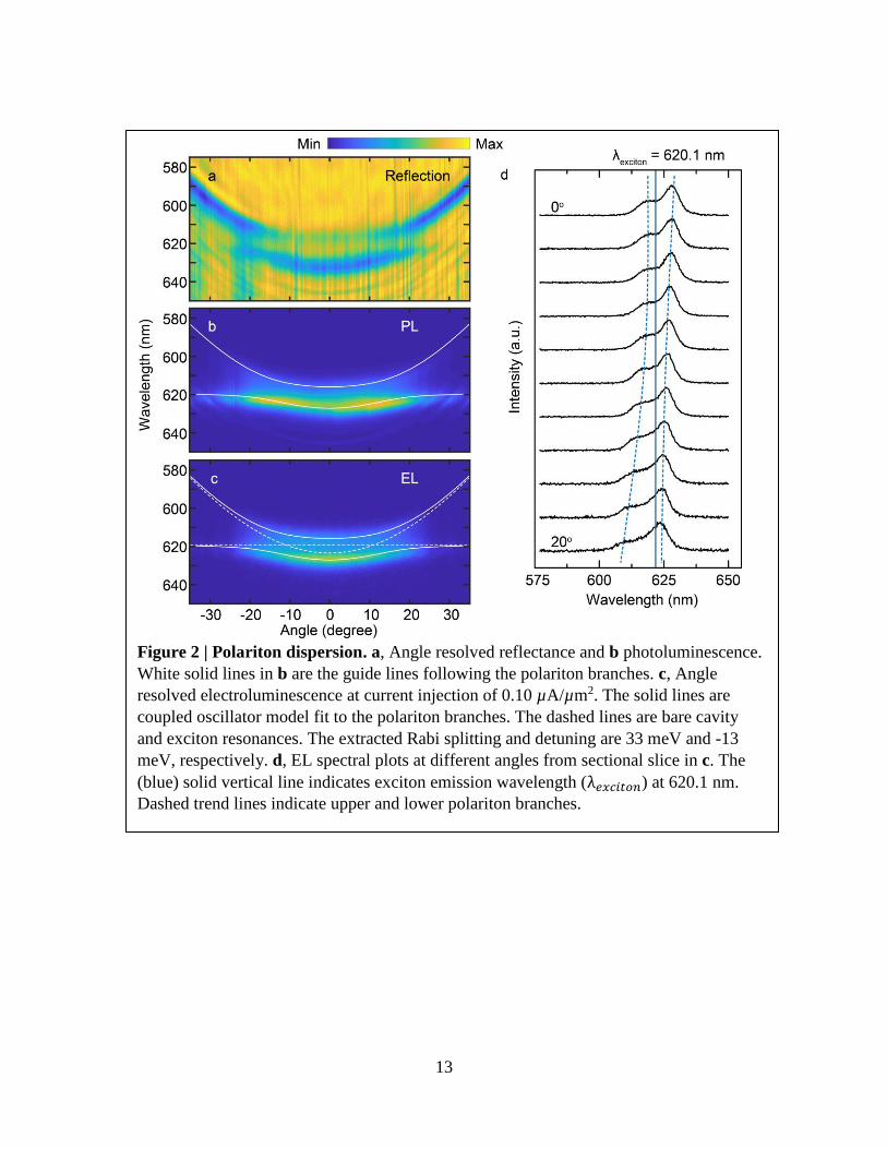
map out the energy versus in-plane momentum dispersion. Figure 2a shows the angle resolved
reflection spectra from the active area of our device demonstrating an anti-crossing behavior. We
further observed photoluminescence (PL) under non-resonant excitation (460 nm) showing an
intense emission from the lower polariton branch and weaker emission from the upper polariton
branch as shown in Fig. 2b (see Methods section for optical measurement details). The EL
measurements are carried out under an external dc bias applied using a Keithley 2400 source meter.
The angle resolved dispersion of polariton EL at 0.1 µA/µm2 injection is shown in Fig. 2c and is
found to be identical to the PL dispersion (Fig. 2b). Spatial image of the EL is shown in
Supplementary Section S3. The Rabi splitting, and cavity detuning derived using coupled oscillator
mode fit (shown by solid and dashed white lines) to the EL experiment is ∼ 33 meV and ∼ -13
meV, respectively. The cavity detuning is defined by δ = 𝐸𝑐 − 𝐸𝑥, where 𝐸𝑥 is the exciton energy
and 𝐸𝑐 stands for cavity photon energy with zero in-plane momentum. The sectional slice, at
different angles, from the EL dispersion is shown in Fig. 2d. The dispersion of the upper and lower
polariton modes can be clearly seen here with the anticrossing occurring in the vicinity of the
exciton resonance (solid line).
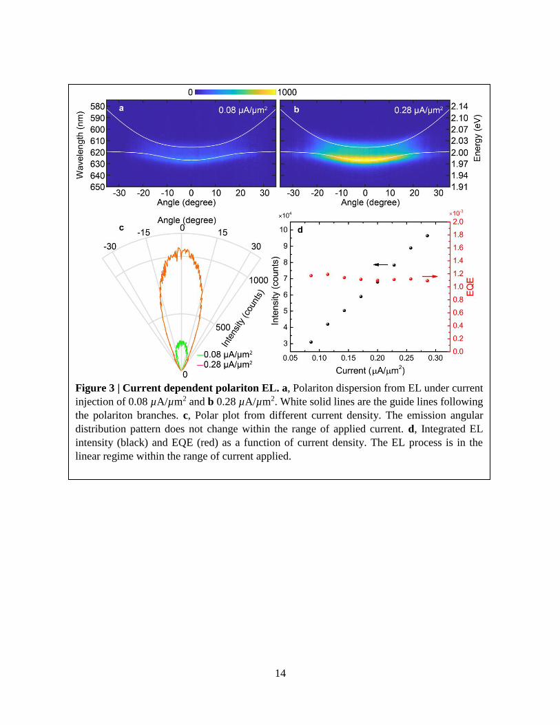
As the tunneling current is increased, the overall intensity of EL goes up. Weak EL from the
polaritons is observed near threshold bias (Fig. 3a), while at sufficiently higher bias above the
threshold, the polaritonic emission becomes distinctively bright (Fig. 3b). Shown in Fig. 3c is the
polar plot of EL intensity as a function of angle depicting a narrow emission cone of ±15o. The
radiation pattern remaining almost unchanged for both minimum (green curve) and maximum
(orange curve) driving current. The integrated intensity under different driving tunnel currents is
shown in Fig. 3d (black dot, left axis) and follows an almost linear trend. Increasing current to
sufficiently higher values could lead to successful polariton scattering along the lower branch and
create extremely narrow emission pattern due to polariton lasing. However, in our case we were
limited by the dielectric breakdown of hBN tunneling barrier and hence could not reach this
regime. Improvement in the quality of hBN could further increase the damage threshold. The
external quantum efficiency (EQE) which is the ratio of the number of extracted photons to the
number of injected charge particles, is also plotted in Fig. 3d (red dots, right axis) as a function of

5
current density. The observed EQE is comparable to other reports of polariton LEDs such as in
organic materials 13 and carbon nanotubes14, albeit the light emitting layer of the present device is
only few atom layer thick (~0.7nm) compared to the much thicker active material used in previous
demonstrations. It should however be noted that the observed EQE is lower than that reported for
similar tunneling devices not confined a cavity geometry11,40. The reduced efficiency is likely due
to the poor light extraction from our cavity, which needs further improvement as well as in-plane
waveguiding. An alternative way to increase EQE is to stack more monolayers inside the tunnel
region separated by thin hBN11. Details of the EQE estimation is given in Supplementary
Information Section S5.
We also investigated the effect of the cavity detuning on the polariton EL by fabricating a similar
device but with a larger cavity detuning (- 43 meV). Further details of this device (Device 2) are
discussed in Supplementary Section S4. Figure 4a shows the angle resolved EL spectra from the
highly negatively detuned device at a current density of 0.2 µA/µm2. Owing to the larger detuning,
this device shows a strong bottle neck effect in the EL with the emission maximum occurring at a
large angle. This is further confirmed in Fig. 4b which compares the normalized polar plot from
Device 2 with that obtained from Device 1 (Fig. 2c). For the higher negative detuning, emission
maximum occurs at 18 degrees (blue curve) as compared with device 1 (orange curve) which
centers at 0 degree. This bottleneck effect for the larger detuning sample can be understood as a
result of poor polariton scattering to k|| = 0 owing to the short polariton lifetime in these cavities.
In summary, we have demonstrated room temperature polariton EL from a vdW heterostructure
embedded in a microcavity. The tunneling architecture of our device enables electron/hole
injection and recombination in WS2 monolayer, which acts as the light emitting layer. The
tunneling mechanism of the device does not require any doping of the constituents, thus
minimizing losses and temperature related variations. The entire tunnel LED comprising of few
layer graphene contacts, hBN tunnel barriers and encapsulating layers are embedded in a
microcavity and the strong coupling regime is achieved as indicated by the presence of the two
polariton branches in reflectivity, PL and EL. Above certain threshold bias, the bands are aligned

6
and favors carrier tunneling from graphene electrodes to the monolayer WS2 through the ultrathin
hBN barriers. Varying current injection above the threshold leads to significant increase in
emission intensity. The EL is also found to be highly directional owing to the cavity dispersion.
Further improvement in cavity Q factor and higher current injection should help realize more
efficient microcavity LEDs and the possibility of an electrically driven low-threshold microcavity
polariton and/or a photon laser. The present demonstration of EL from TMD exciton-polaritons in
a microcavity is a significant progress towards realizing such electrically driven integrated
microcavity light emitters using 2D vdW materials for potential application as ultrafast LEDs and
low threshold lasers.
Methods:
Sample Preparation. The DBR consisting of 12 periods of alternate layers of SiO2 (106.2 nm) and
Si3N4 (77.5 nm) was grown on silicon substrate by plasma enhanced chemical vapor deposition
(PECVD) using a combination of nitrous oxide, silane and ammonia under a temperature of 350°C.
Two gold contacts were then prefabricated onto the DBR top surface. We used electron beam
lithography to write the contacts pattern and deposited Ti/Au (2nm/8nm) by electron beam
evaporation. Monolayer WS2, graphene and multilayer hBN were exfoliated from bulk crystals
(WS2 and graphene from HQ Graphene and hBN from 2Dsemiconductor Inc.) using scotch tape f
onto 300nm SiO2/Si substrate. Heterostructure stacking and transfer were done using the well-
known poly-propylene carbonate (PPC) transfer technique41. We first identified a thick hBN layer
(40nm) and then used it to stack the top two WS2 monolayers followed by stacking the tunnel
region. The final stack structure from top to bottom is hBN / WS2 / hBN / WS2 / hBN / graphene /
hBN / WS2 / hBN / graphene / hBN. There are 11 separate layers and the stacking was done
continuously from top to bottom. Several stacking images are shown in Supplementary Section
S2. The entire stack of van der Waal heterostructure was then transferred onto the DBR at
temperature 120 ℃. Alignment was carefully done to make sure each graphene flake sits exactly
on top of corresponding gold contact pad. After the transfer, the entire structure was soaked in
chloroform for 2 hours to remove PPC residue followed by PMMA (495 A4 from Michrochem)

7
spin coating to form a 200 nm top spacer layer. The final silver (40 nm) was deposited via e-beam
evaporation for the top mirror of the microcavity. Details of each layer thickness and cavity
response can be found in Supplementary Section S1.
Optical measurement Angle resolved spectra were recorded using a homemade setup comprising
of white light (broad band halogen source for reflection) and laser (PL measurement). The setup is
coupled with Princeton Instruments monochromator with a PIXIS: 256 EMCCD camera. A 100X,
0.7 NA objective was used for all measurements. The polariton dispersion is revealed by imaging
the back aperture of the microscope objective (Fourier plane) on to the camera. All measurements
were done at room temperature.

8
1. Kasprzak, J., Richard, M., Kundermann, S., Baas, A., Jeambrun, P., Keeling, J. M. J.,
Marchetti, F. M., Szymańska, M. H., André, R., Staehli, J. L., Savona, V., Littlewood, P.
B., Deveaud, B. & Dang, L. S. Bose-Einstein condensation of exciton polaritons. Nature
443, 409–414 (2006).
2. Balili, R., Hartwell, V., Snoke, D., Pfeiffer, L. & West, K. Bose-Einstein Condensation of
Microcavity Polaritons in a Trap. Science 316, 1007–1010 (2007).
3. Deng, H., Weihs, G., Santori, C., Bloch, J. & Yamamoto, Y. Condensation of
Semiconductor Microcavity Exciton Polaritons. Science 298, 199–202 (2002).
4. Berloff, N. G., Silva, M., Kalinin, K., Askitopoulos, A., Töpfer, J. D., Cilibrizzi, P.,
Langbein, W. & Lagoudakis, P. G. Realizing the classical XY Hamiltonian in polariton
simulators. Nat. Mater. 16, 1120–1126 (2017).
5. Amo, A. & Bloch, J. Exciton-polaritons in lattices: A non-linear photonic simulator.
Comptes Rendus Phys. 17, 934–945 (2016).
6. Sturm, C., Tanese, D., Nguyen, H. S., Flayac, H., Galopin, E., Lemaître, A., Sagnes, I.,
Solnyshkov, D., Amo, A., Malpuech, G. & Bloch, J. All-optical phase modulation in a
cavity-polariton Mach-Zehnder interferometer. Nat. Commun. 5, 3278 (2014).
7. Schneider, C., Glazov, M. M., Korn, T., Höfling, S. & Urbaszek, B. Two-dimensional
semiconductors in the regime of strong light-matter coupling. Nat. Commun. 9, 2695
(2018).
8. Hofling, S., Amthor, M., Rahimi-Iman, A., Kim, N. Y., Fischer, J., Savenko, I. G.,
Kulakovski, V. D., Shelykh, I. a., Reitzenstein, S., Forchel, A., Yamamoto, Y., Kamp, M.
& Schneider, C. An electrically pumped polariton laser. Nature 497, 348–352 (2013).
9. Bhattacharya, P., Frost, T., Deshpande, S., Baten, M. Z., Hazari, A. & Das, A. Room
temperature electrically injected polariton laser. Phys. Rev. Lett. 112, 29–31 (2014).
10. Tsonev, D., Videv, S. & Haas, H. Light fidelity (Li-Fi): towards all-optical networking. in
SPIE OPTO (eds. Dingel, B. B. & Tsukamoto, K.) 900702 (International Society for
Optics and Photonics, 2013). doi:10.1117/12.2044649
11. Withers, F., Del Pozo-Zamudio, O., Mishchenko, A., Rooney, A. P., Gholinia, A.,
Watanabe, K., Taniguchi, T., Haigh, S. J., Geim, A. K., Tartakovskii, A. I. & Novoselov,
K. S. Light-emitting diodes by band-structure engineering in van der Waals
heterostructures. Nat. Mater. 14, 301–306 (2015).
12. Withers, F., Del Pozo-Zamudio, O., Schwarz, S., Dufferwiel, S., Walker, P. M., Godde,
T., Rooney, A. P., Gholinia, A., Woods, C. R., Blake, P., Haigh, S. J., Watanabe, K.,
Taniguchi, T., Aleiner, I. L., Geim, A. K., Fal’ko, V. I., Tartakovskii, A. I. & Novoselov,

9
K. S. WSe2 Light-Emitting Tunneling Transistors with Enhanced Brightness at Room
Temperature. Nano Lett. 15, 8223–8228 (2015).
13. Gubbin, C. R., Maier, S. A. & Kéna-Cohen, S. Low-voltage polariton electroluminescence
from an ultrastrongly coupled organic light-emitting diode. Appl. Phys. Lett. 104, 233302
(2014).
14. Graf, A., Held, M., Zakharko, Y., Tropf, L., Gather, M. C. & Zaumseil, J. Electrical
pumping and tuning of exciton-polaritons in carbon nanotube microcavities. Nat. Mater.
16, 911–917 (2017).
15. Choi, W., Choudhary, N., Han, G. H., Park, J., Akinwande, D. & Lee, Y. H. Recent
development of two-dimensional transition metal dichalcogenides and their applications.
Mater. Today 20, 116 (2017).
16. Chen, Y. J., Cain, J. D., Stanev, T. K., Dravid, V. P. & Stern, N. P. Valley-polarized
exciton-polaritons in a monolayer semiconductor. Nat. Photonics 11, 431–435 (2017).
17. Dufferwiel, S., Lyons, T. P., Solnyshkov, D. D., Trichet, A. A. P., Withers, F., Schwarz,
S., Malpuech, G., Smith, J. M., Novoselov, K. S., Skolnick, M. S., Krizhanovskii, D. N. &
Tartakovskii, A. I. Valley-addressable polaritons in atomically thin semiconductors. Nat.
Photonics 11, 497–501 (2017).
18. Sun, Z., Gu, J., Ghazaryan, A., Shotan, Z., Considine, C. R., Dollar, M., Chakraborty, B.,
Liu, X., Ghaemi, P., Kéna-Cohen, S. & Menon, V. M. Optical control of room-
temperature valley polaritons. Nat. Photonics 11, 491–496 (2017).
19. Sidler, M., Back, P., Cotlet, O., Srivastava, A., Fink, T., Kroner, M., Demler, E. &
Imamoglu, A. Fermi polaron-polaritons in charge-tunable atomically thin semiconductors.
Nat. Phys. 13, 255–261 (2016).
20. Dhara, S., Chakraborty, C., Goodfellow, K. M., Qiu, L., O’Loughlin, T. A., Wicks, G. W.,
Bhattacharjee, S. & Vamivakas, A. N. Anomalous dispersion of microcavity trion-
polaritons. Nat. Phys. 14, 130–133 (2017).
21. Lundt, N., Nagler, P., Nalitov, A., Klembt, S., Wurdack, M., Stoll, S., Harder, T. H.,
Betzold, S., Baumann, V., Kavokin, A. V, Schüller, C., Korn, T., Höfling, S. & Schneider,
C. Valley polarized relaxation and upconversion luminescence from Tamm-plasmon
trion–polaritons with a MoSe2 monolayer. 2D Mater. 4, 25096 (2017).
22. Sanvitto, D. & Kéna-Cohen, S. The road towards polaritonic devices. Nat. Mater. 15,
1061–1073 (2016).
23. Liew, T. C. H., Kavokin, A. V & Shelykh, I. A. Optical Circuits Based on Polariton
Neurons in Semiconductor Microcavities. Phys. Rev. Lett. 101, 16402 (2008).

10
24. Lu, T. C., Chen, J. R., Lin, S. C., Huang, S. W., Wang, S. C. & Yamamoto, Y. Room
temperature current injection polariton light emitting diode with a hybrid microcavity.
Nano Lett. 11, 2791–2795 (2011).
25. Bajoni, D., Semenova, E., Lemaître, A., Bouchoule, S., Wertz, E., Senellart, P. & Bloch,
J. Polariton light-emitting diode in a GaAs-based microcavity. Phys. Rev. B 77, 113303
(2008).
26. Zhang, Z., Wang, Y., Yin, S., Hu, T., Wang, Y., Liao, L., Luo, S., Wang, J., Zhang, X.,
Ni, P., Shen, X., Shan, C. & Chen, Z. Exciton-polariton light-emitting diode based on a
ZnO microwire. Opt. Express 25, 17375–17381 (2017).
27. Tsintzos, S. I., Pelekanos, N. T., Konstantinidis, G., Hatzopoulos, Z. & Savvidis, P. G. A
GaAs polariton light-emitting diode operating near room temperature. Nature 453, 372–
375 (2008).
28. Khalifa, A. A., Love, A. P. D., Krizhanovskii, D. N., Skolnick, M. S. & Roberts, J. S.
Electroluminescence emission from polariton states in GaAs-based semiconductor
microcavities. Appl. Phys. Lett. 92, 61107 (2008).
29. Tischler, J. R., Bradley, M. S., Bulović, V., Song, J. H. & Nurmikko, A. Strong coupling
in a microcavity LED. Phys. Rev. Lett. 95, 36401 (2005).
30. Lodden, G. H. & Holmes, R. J. Electrical excitation of microcavity polaritons by radiative
pumping from a weakly coupled organic semiconductor. Phys. Rev. B 82, 125317 (2010).
31. Christogiannis, N., Somaschi, N., Michetti, P., Coles, D. M., Savvidis, P. G., Lagoudakis,
P. G. & Lidzey, D. G. Characterizing the Electroluminescence Emission from a Strongly
Coupled Organic Semiconductor Microcavity LED. Adv. Opt. Mater. 1, 503–509 (2013).
32. Lee, B., Liu, W., Naylor, C. H., Park, J., Malek, S. C., Berger, J. S., Johnson, a. T. C. &
Agarwal, R. Electrical Tuning of Exciton-Plasmon Polariton Coupling in Monolayer
MoS2 Integrated with Plasmonic Nanoantenna Lattice. Nano Lett. 17, 4541–4547 (2017).
33. Chakraborty, B., Gu, J., Sun, Z., Khatoniar, M., Bushati, R., Boehmke, A. L., Koots, R. &
Menon, V. M. Control of Strong Light–Matter Interaction in Monolayer WS2 through
Electric Field Gating. Nano Lett. 18, 6455–6460 (2018).
34. Zhong, D., Seyler, K. L., Linpeng, X., Cheng, R., Sivadas, N., Huang, B., Schmidgall, E.,
Taniguchi, T., Watanabe, K., McGuire, M. A., Yao, W., Xiao, D., Fu, K.-M. C. & Xu, X.
Van der Waals engineering of ferromagnetic semiconductor heterostructures for spin and
valleytronics. Sci. Adv. 3, e1603113 (2017).
35. Xi, X., Zhao, L., Wang, Z., Berger, H., Forró, L., Shan, J. & Mak, K. F. Strongly
enhanced charge-density-wave order in monolayer NbSe2. Nat. Nanotechnol. 10, 765–769
(2015).

11
36. Wang, Z., Gresch, D., Soluyanov, A. A., Xie, W., Kushwaha, S., Dai, X., Troyer, M.,
Cava, R. J. & Bernevig, B. A. MoTe2: A Type-II Weyl Topological Metal. Phys. Rev.
Lett. 117, 56805 (2016).
37. Sundaram, R. S., Engel, M., Lombardo, A., Krupke, R., Ferrari, A. C., Avouris, P. &
Steiner, M. Electroluminescence in Single Layer MoS2. Nano Lett. 13, 1416–1421 (2013).
38. Ross, J. S., Klement, P., Jones, A. M., Ghimire, N. J., Yan, J., Mandrus, D. G., Taniguchi,
T., Watanabe, K., Kitamura, K., Yao, W., Cobden, D. H. & Xu, X. Electrically tunable
excitonic light-emitting diodes based on monolayer WSe2 p–n junctions. Nat.
Nanotechnol. 9, 268–272 (2014).
39. Cheng, R., Li, D., Zhou, H., Wang, C., Yin, A., Jiang, S., Liu, Y., Chen, Y., Huang, Y. &
Duan, X. Electroluminescence and Photocurrent Generation from Atomically Sharp
WSe2/MoS2 Heterojunction p–n Diodes. Nano Lett. 14, 5590–5597 (2014).
40. Wang, S., Wang, J., Zhao, W., Giustiniano, F., Chu, L., Verzhbitskiy, I., Zhou Yong, J. &
Eda, G. Efficient carrier-to-exciton conversion in field emission tunnel diodes based on
MIS-Type van der waals heterostack. Nano Lett. 17, 5156–5162 (2017).
41. Wang, L., Meric, I., Huang, P. Y., Gao, Q., Gao, Y., Tran, H., Taniguchi, T., Watanabe,
K., Campos, L. M., Muller, D. A., Guo, J., Kim, P., Hone, J., Shepard, K. L. & Dean, C.
R. One-Dimensional Electrical Contact to a Two-Dimensional Material. Science 342,
614–617 (2013).
Data Availability: Data are available on request from the authors
Acknowledgements: We acknowledge support from the National Science Foundation through the
EFRI-2DARE program (EFMA-1542863), MRSEC program 420634 and the ARO MURI
program (W911NF-17-1-0312). The authors also acknowledge the use of the Nanofabrication
Facility at the CUNY Advanced Science Research Center for the fabrication of the devices.
Author Contributions:
V.M., J.G., B.C. conceived the experiments. J.G., B.C. M.K. fabricated the devices and performed
the measurements. B.C., J.G., V.M. performed data analysis. All authors contributed to write the
manuscript and discuss the results.
Competing Interests: The authors declare that they have no competing financial interests.

12
Figure 1 | Device schematic and tunneling mechanism. a, Schematic of the device.
Thickness of each layer can be found in Supplementary Section S1. b, Optical image of the
stacking before the top cavity is grown. Gold contacts and top hBN are labeled. Due to the
large reflection from DBR substrate, only top hBN is observable. More images of sample
fabrication is shown in Supplementary Section S2. c, Band diagrams at high bias above
threshold. Electron (hole) can tunnel through hBN into WS2 conduction (valence) band.
Top (bottom) graphene is labeled as GrT (GrB). d, Tunneling current as a function of bias
voltage.
a b
c d
13
Figure 2 | Polariton dispersion. a, Angle resolved reflectance and b photoluminescence.
White solid lines in b are the guide lines following the polariton branches. c, Angle
resolved electroluminescence at current injection of 0.10 µA/µm2. The solid lines are
coupled oscillator model fit to the polariton branches. The dashed lines are bare cavity
and exciton resonances. The extracted Rabi splitting and detuning are 33 meV and -13
meV, respectively. d, EL spectral plots at different angles from sectional slice in c. The
(blue) solid vertical line indicates exciton emission wavelength (λ𝑒𝑥𝑐𝑖𝑡𝑜𝑛) at 620.1 nm.
Dashed trend lines indicate upper and lower polariton branches.
14
Figure 3 | Current dependent polariton EL. a, Polariton dispersion from EL under current
injection of 0.08 µA/µm2 and b 0.28 µA/µm2. White solid lines are the guide lines following
the polariton branches. c, Polar plot from different current density. The emission angular
distribution pattern does not change within the range of applied current. d, Integrated EL
intensity (black) and EQE (red) as a function of current density. The EL process is in the
linear regime within the range of current applied.

15
Figure 4 | Detuning dependence on EL. a, Device 2 angle resolved EL (0.2 µA/µm2)
with a large negative detuning (-43 meV). A strong bottle neck effect was observed. b,
Normalized angular emission pattern from device 1 (Fig. 2c) and device 2 (Fig. 4a)
showing distinct emission patterns owing to the difference in detuning.

Table of Contents
S1. Cavity mode distribution ................................................................................................................... 2
S2. More Stacking images ....................................................................................................................... 3
S3. EL spacial image ................................................................................................................................. 4
S4. Device 2 data ..................................................................................................................................... 5
S5. External Quantum efficiency ............................................................................................................. 8

S1. Cavity mode distribution
Figure S1 | Device schematic and cavity resonance. a, Device schematic. b, Mode distribution for
wavelength at 620.1nm which is the WS2 exciton energy. Position ‘0’ relates to the top surface which is
silver. Thickness of the cavity is tuned to have the mode profile’s second maximum position falling on the
WS2 region. Inset shows the bare cavity mode with 8.2nm (24meV) linewidth.
Material Silver PMMA hBN WS2 hBN WS2 hBN Graphene hBN WS2 hBN Graphene hBN SiO2 DBR-SiNx DBR-SiO2
Thickness (nm)
40 200 40 0.7 2 0.7 3 0.4 2 0.7 2 0.4 20 78 77.5 106.2
Table S1 | Thickness of each layer in Figure S1a.
(a) (b)

S2. Stacking images
This section shows the optical images of stacking steps after each WS2 layer was picked up.
Stacking order Image on PPC film WS2 image
1. First WS2
2. Second WS2
3. Third WS2
Table S2 | Optical images of the stacking at different steps. Left: Schematics of the stacked layer order.
Middle: Optical image of the PPC film at different steps. Right: Microscope optical image of different WS2
layers. In each row, there are two white arrows in middle and right columns pointing at the same position
for the guiding of view to ensure the WS2 has been successfully picked up at each step. Monolayer WS2 is
easy to identify due to the color contrast, for example, in the first WS2 image, the white arrow is pointing
at the monolayer region. All the figures have the same scale. A 10 µm scale bar is shown in the first row
PPC film image.
Only part of this WS2 is picked up

S3. EL spatial image
Figure S3 | EL spatial image. a, Sample optical image on the PPC film after the third WS2 layer was picked
up. The graphene (long dash) and gold contacts (short dash) outlines are labeled with different colors. The
scale bar is 10µm. All the images have the same scale bar. b, Optical image of the third WS2 layer on SiO2/Si
substrate before the picking up. There is a small bilayer region shown by the white arrow. c, EL spacial
image at 0.28 µA/µm2. Because only the third WS2 layer is inside the tunneling region, as shown in Table
S2, row 3, when a bias is applied across the graphene contacts, only the third layer WS2 will show EL. The
bilayer region in the third WS2 shows much less EL due to its indirect band gap.
a b c

S4. Device 2 data
We made another device by first stacking and transferring the tunneling structure, which has only one
WS2 monolayer inside, followed by stacking and transferring another top two WS2 monolayers
(hBN/WS2/hBN/WS2), unlike the device 1 stacking steps, which stacked the top two WS2 layers first and
then stacked the tunneling structure. The final structure of device 2 is the same as device 1 as shown in
Fig. S1a. The only difference is that the third hBN (count from top to bottom) layer thickness is 30 nm
because this hBN layer acts as the first picking up layer for the tunneling structure in device 2. The rest of
PMMA and SiO2 thickness were also tuned to match to mode position. One of the advantages of trying
this method is that, by separating the stacking process into two (one has 7 stacking layers, another has 4
stacking layers), the device fabrication will have a much higher success rate. The original stacking
encounters continuous 11 layers with much higher chance of damaging the thin graphene contact by more
stacking-picking up process. Images of the first stacking process which evolves 7 stacking layers are shown
in Table S4 (below). Device 2 also shows strong coupling with Rabi splitting 27meV.
Stacking order Stacking image Current stacked layer image
1.
2.
hBN
Graphene

3.
4.
5.
6.
Table S4 | Device 2 stacking images.
WS2 Only part of WS2 is picked up
hBN
Graphene
hBN

Figure S4 | Angle resolved spectra from device 2. Angle resolved reflection (a) PL (b) EL (c) spectra. d, EL
linecut from 10 degree to 35 degree showing 27 meV Rabi splitting.

S5. External Quantum efficiency
The external quantum efficiency (EQE) is defined as the number of photon emitted per tunneling carrier
Ne/i (N is the photon emitted every second from the total tunneling monolayer WS2 area, e is the
electron charge, i the current passing through the total tunneling monolayer WS2 area). N is defined as
N =𝑁𝑑𝑒𝑡𝑒𝑐𝑡𝑒𝑑
𝛼𝑡𝑜𝑡𝑎𝑙
Ndetected is the intensity detected by the detector per second from WS2 tunneling emission. 𝛼𝑡𝑜𝑡𝑎𝑙 is the
total collection efficiency of the whole system. Light emitted from monolayer is collected by an objective
with N.A 0.7 and guided through mirrors and lenses into the detector. The detector is set to a high gain
factor. All those will affect the actual counts read by the detector. In order to know N, we need to
measure 𝛼𝑡𝑜𝑡𝑎𝑙 for a given set up that is exactly the same as the one we use to detect the tunneling
emission. We did this by shining a laser that has the same wavelength (620.1nm) as our tunneling emission
to a perfect reflector and the reflected beam was guided along the same path as the tunneling emission
into the detector. The laser power on the reflection standard surface is measured to be 𝑃. The measured
laser counts is 𝑁𝑙𝑎𝑠𝑒𝑟 per second. 𝛼𝑡𝑜𝑡𝑎𝑙 is calculated as:
𝛼𝑡𝑜𝑡𝑎𝑙 = 𝑁𝑙𝑎𝑠𝑒𝑟
𝑃∗ 𝐸
E is the laser energy which is 2 eV.
So N is:
N =𝑁𝑑𝑒𝑡𝑒𝑐𝑡𝑒𝑑
𝑁𝑙𝑎𝑠𝑒𝑟 ∗ 𝐸∗ 𝑃