a routing algorithm for flip-chip designcc.ee.ntu.edu.tw/~ywchang/papers/iccad05-fc.pdf · a...
TRANSCRIPT

A Routing Algorithm for Flip-Chip Design
Jia-Wei Fang1, I-Jye Lin2, Ping-Hung Yuh3, Yao-Wen Chang1,2, and Jyh-Herng Wang41Graduate Institute of Electronics Engineering, National Taiwan University, Taipei 106, Taiwan
2Department of Electrical Engineering, National Taiwan University, Taipei 106, Taiwan3Department of Computer Science and Information Engineering, National Taiwan University, Taipei 106, Taiwan
4Faraday Technology Corporation, Hsinchu 300, Taiwan
Abstract— The flip-chip package gives the highest chip density of anypackaging method to support the pad-limited Application-Specific Inte-grated Circuit (ASIC) designs. In this paper, we propose thefirst routerfor the flip-chip package in the literature. The router can redistribute netsfrom wire-bonding pads to bump pads and then route each of them. Therouter adopts a two-stage technique of global routing followed by detailedrouting. In global routing, we use the network flow algorithm to solvethe assignment problem from the wire-bonding pads to the bump pads,and then create the global routing path for each net. The detailed routingconsists of three stages, cross point assignment, net ordering determination,and track assignment, to complete the routing. Experimental results basedon seven real designs from the industry demonstrate that therouter canreduce the total wirelength by 10.2%, the critical wirelength by 13.4%, andthe signal skews by 13.9%, compared with a heuristic algorithm currentlyused in industry.
I. INTRODUCTION
A. Flip-Chip DesignDue to the increasing complexity and decreasing feature size of Very
Large Scale Integration (VLSI) designs, the demand of more I/O pads hasbecome a significant problem of package technologies. A relatively newpackaging technology, theflip-chip (FC) package, as shown in Figure 1, iscreated for higher integration density and rising power consumption. Flip-chip bonding was first developed by IBM in 1960’s. It gives the highestchip density of any packaging method to support the pad-limited ASICdesigns.
Bump Ball
Wire-bonding PadDie
Bump Pad
(a)
Mold Cap
Solder Ball Rigid Laminate(b)
Fig. 1. (a) A Flip Chip. (b) A Flip Chip Package.
Flip-chip is not a specific package, or even a package type (like PGAor BGA). Flip-chip describes the method of electrically connecting the dieto the package carrier. The package carrier, either a substrate or a lead-frame, provides the connection from the die to the outside devices of thepackage. The die is attached to the carrier face up, and latera wire isbonded first to the die, then looped and bonded to the carrier. In contrast,the interconnection between the die and carrier in the flip-chip package ismade through a conductive bump ball that is placed directly on the diesurface. Finally, the bumped die is flipped over and placed facedown, withthe bump balls connecting to the carrier directly. The flip-chip technology isthe choice in high-speed applications because of the following advantages:reduced signal inductance (high speed), reduced power/ground inductance(low power), reduced package footprint, smaller die size, higher signaldensity, and lower thermal effect. However, in recent IC designs, the I/Opads are still placed along the boundary of the die. This placement does notsuit for the flip-chip package. As a result, we use the top metal or an extra
metal layer, called aRe-Distributed Layer (RDL)as shown in Figure 2, toredistribute thewire-bonding padsto thebump padswithout changing theplacement of the I/O pads. Since the RDL is the top metal layer of the die,the routing angle in an RDL cannot be any-angle. Bump balls areplacedon the RDL and use the RDL to connect to wire-bonding pads by bumppads.
M7
(Top Metal)
PASV(L3)
M1
Bump
Other routing under bump
Top Metal
IO bufferCore cells
Redistributed Layer
M7
(Top Metal)
PASV(L3)
M1
Bump
Other routing under bump
Top Metal
IO bufferCore cells
Redistributed Layer
Fig. 2. Cross Section of RDL
The flip-chip package is generally classified into two types: thepe-ripheral array as shown in Figure 3(a) and thearea array as shown inFigure 3(b). In the peripheral array, the bump balls are placed along theboundary of the flip-chip package. The disadvantage of the peripheral arrayis that we only have the limited number of bump balls. In the area array,the bump balls are placed in the whole area of the flip-chip package. Theadvantage of the area array is that the number of bump balls is much morethan that of the peripheral array, so it is more suitable for modern VLSIdesigns. Since the flip-chip design is for high speed circuits, theissue ofsignal skews is also important. Thus a special router, theRedistributionLayer (RDL) router[13], is needed to reroute the peripheral wire-bondingpads to the bump pads and then connect the bump pads to the bumpballs. Considering the routing of multi-pin nets and the minimization oftotal wirelength and the signal skews are also needed for an RDL router.Figure 3(c) shows one RDL routing result for an area-array flip-chip.
Die
Bump Ball(a) (b) (c)
Fig. 3. (a) A Peripheral Array. (b) An Area Array. (c) An RDL Routing Result.
B. Previous WorkTo the best knowledge of the authors, there is no previous work in the
literature on the routing problem for flip-chip designs. Similar works arethe routing for ball grid array (BGA) packages and pin grid array (PGA)packages, including [3], [10], [11], [12], [14], [16] and [17]. The work [16]used the geometric and symmetric attributes of the pin positions intheBGA packages to assign pins of the BGA. However, in flip-chip designsthe positions of wire-bonding pads and bump pads do not always have thesegeometric and symmetric attributes. The works [3] and [11] presented PGArouters while [12] provided a BGA router. These three routersare any-angle, multi-layer routers without considering the pin assignment problem,single-layer routing, and total wirelength minimization. Theworks [14]and [17] applied the minimum-cost network flow algorithm to solve the
I/O pin routing problems. All these routers focused only on routability anddid not consider multi-pin nets and signal skews. The work [14] alsodidnot consider the routing congestion problem. Furthermore, theyassumedthat wires can be any-angle, so their methods are not suitable for the RDLrouting, typically with 90-degree angle routing.
C. Our ContributionsTo our best knowledge, this paper is the first work in the literature
to propose an RDL router to handle the routing problem of flip-chipdesigns with real industry applications. We present a unified network-flowformulation to simultaneously consider the assignment of the wire-bondingpads to the bump pads and the routing between them. Our algorithm consistsof two phases. The first phase is the global routing that assigns eachwire-bonding pad to a unique bump pad. By formulating the assignment as amaximum flow problem and applying the minimum-cost maximum-flowalgorithm, we can guarantee 100% detailed routing completionafter theassignment. The second phase is the detail routing that efficiently distributesthe routing points between two bump pads and assigns wires into tracks.In addition to the traditional single-layer routing with only routabilityoptimization, our RDL router also tries to optimize the total wirelengthand the signal skews between a pair of signal nets under the 100% routingcompletion constraint. Experimental results based on seven real designsfrom the industry demonstrate that the router can reduce the total wirelengthby 10.2%, the critical wirelength by 13.4%, and the signal skews by 13.9%,compared with a heuristic algorithm currently used in industry.
The rest of this paper is organized as follows. Section 2 gives theformulation of the RDL routing problem. Section 3 details our globaland detailed routing algorithms. Section 4 shows the experimental results.Finally, conclusions are given in section 5.
II. PROBLEM FORMULATION
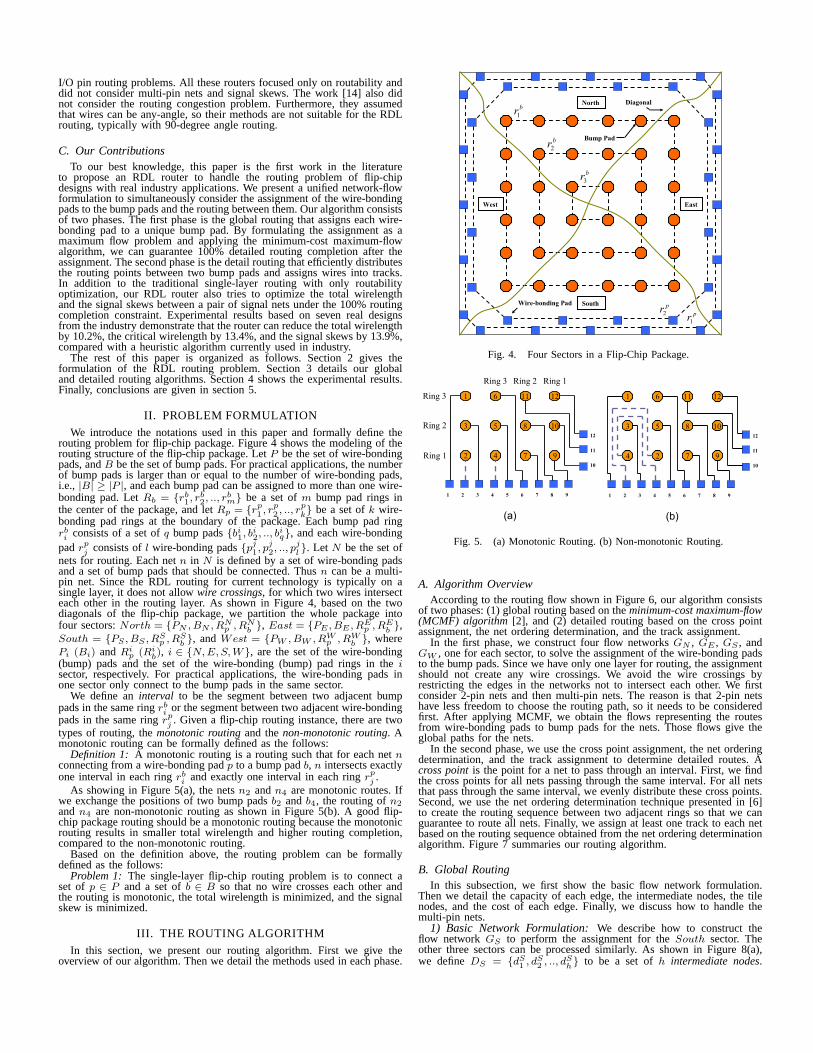
We introduce the notations used in this paper and formally define therouting problem for flip-chip package. Figure 4 shows the modeling of therouting structure of the flip-chip package. LetP be the set of wire-bondingpads, andB be the set of bump pads. For practical applications, the numberof bump pads is larger than or equal to the number of wire-bonding pads,i.e., |B| ≥ |P |, and each bump pad can be assigned to more than one wire-bonding pad. LetRb = {rb
1, rb
2, .., rb
m} be a set ofm bump pad rings inthe center of the package, and letRp = {rp
1, r
p2, .., r
p
k} be a set ofk wire-
bonding pad rings at the boundary of the package. Each bump padringrbi
consists of a set ofq bump pads{bi1, bi
2, .., bi
q}, and each wire-bondingpadr
pj
consists ofl wire-bonding pads{pj1, p
j2, .., p
j
l}. Let N be the set of
nets for routing. Each netn in N is defined by a set of wire-bonding padsand a set of bump pads that should be connected. Thusn can be a multi-pin net. Since the RDL routing for current technology is typically on asingle layer, it does not allowwire crossings, for which two wires intersecteach other in the routing layer. As shown in Figure 4, based on the twodiagonals of the flip-chip package, we partition the whole package intofour sectors:North = {PN , BN , RN
p , RNb}, East = {PE , BE , RE
p , REb},
South = {PS , BS , RSp , RS
b}, andWest = {PW , BW , RW
p , RWb}, where
Pi (Bi) and Rip (Ri
b), i ∈ {N, E, S, W}, are the set of the wire-bonding
(bump) pads and the set of the wire-bonding (bump) pad rings in the isector, respectively. For practical applications, the wire-bonding pads inone sector only connect to the bump pads in the same sector.
We define aninterval to be the segment between two adjacent bumppads in the same ringrb
ior the segment between two adjacent wire-bonding
pads in the same ringrpj. Given a flip-chip routing instance, there are two
types of routing, themonotonic routingand thenon-monotonic routing. Amonotonic routing can be formally defined as the follows:
Definition 1: A monotonic routing is a routing such that for each netnconnecting from a wire-bonding padp to a bump padb, n intersects exactlyone interval in each ringrb
iand exactly one interval in each ringrp
j.
As showing in Figure 5(a), the netsn2 andn4 are monotonic routes. Ifwe exchange the positions of two bump padsb2 andb4, the routing ofn2
and n4 are non-monotonic routing as shown in Figure 5(b). A good flip-chip package routing should be a monotonic routing because the monotonicrouting results in smaller total wirelength and higher routingcompletion,compared to the non-monotonic routing.
Based on the definition above, the routing problem can be formallydefined as the follows:
Problem 1: The single-layer flip-chip routing problem is to connect aset of p ∈ P and a set ofb ∈ B so that no wire crosses each other andthe routing is monotonic, the total wirelength is minimized, and the signalskew is minimized.
III. THE ROUTING ALGORITHM
In this section, we present our routing algorithm. First we give theoverview of our algorithm. Then we detail the methods used in each phase.
Bump Pad
Wire-bonding Pad
North
EastWest
South
Diagonalbr1
br2
br3
pr1
pr2
Fig. 4. Four Sectors in a Flip-Chip Package.
4 7 9
1 2 3 4 5 6 7 8 9
10
11
2
3
6 11 12
5 8 1012
1Ring 3
Ring 3 Ring 2 Ring 1
Ring 2
Ring 1
(a)
2 7 9
2 3 4 6 7 8 9
10
11
4
3
6 11 12
5 8 10
1
12
1 5
(b)
Fig. 5. (a) Monotonic Routing. (b) Non-monotonic Routing.
A. Algorithm OverviewAccording to the routing flow shown in Figure 6, our algorithm consists
of two phases: (1) global routing based on theminimum-cost maximum-flow(MCMF) algorithm [2], and (2) detailed routing based on the cross pointassignment, the net ordering determination, and the track assignment.
In the first phase, we construct four flow networksGN , GE , GS , andGW , one for each sector, to solve the assignment of the wire-bonding padsto the bump pads. Since we have only one layer for routing, the assignmentshould not create any wire crossings. We avoid the wire crossings byrestricting the edges in the networks not to intersect each other. We firstconsider 2-pin nets and then multi-pin nets. The reason is that 2-pin netshave less freedom to choose the routing path, so it needs to be consideredfirst. After applying MCMF, we obtain the flows representing theroutesfrom wire-bonding pads to bump pads for the nets. Those flows givetheglobal paths for the nets.
In the second phase, we use the cross point assignment, the net orderingdetermination, and the track assignment to determine detailed routes. Across pointis the point for a net to pass through an interval. First, we findthe cross points for all nets passing through the same interval. For all netsthat pass through the same interval, we evenly distribute these cross points.Second, we use the net ordering determination technique presented in [6]to create the routing sequence between two adjacent rings so that we canguarantee to route all nets. Finally, we assign at least one trackto each netbased on the routing sequence obtained from the net ordering determinationalgorithm. Figure 7 summaries our routing algorithm.
B. Global RoutingIn this subsection, we first show the basic flow network formulation.
Then we detail the capacity of each edge, the intermediate nodes, the tilenodes, and the cost of each edge. Finally, we discuss how to handlethemulti-pin nets.
1) Basic Network Formulation:We describe how to construct theflow network GS to perform the assignment for theSouth sector. Theother three sectors can be processed similarly. As shown in Figure 8(a),we defineDS = {dS
1, dS
2, .., dS
h} to be a set ofh intermediate nodes.

Global Routing
Multi -pin Nets Handling
Two-pin Nets Handling
Detailed Routing
Intermediate Nodes &
Tile Nodes Insertion
Graph Contruction
Two-pin Nets Routing
Cost and Capacity
Assginment
Cross Point Assignment
Net Ordering
Determination
Track Assignment
No
Wire-bounding Pad List
Bump Pad List
Net List
Design Rule Checker
Existence of Multi -pin Nets ?
Multi -pin Nets Routing
Yes
Fig. 6. The RDL Routing Flow
Algorithm: RDL Routing( P , B, N )P : set of all wire-bonding pads;B: set of all bump pads;N : set of all nets;1 begin2 Construct four graphsGN , GE , GS , GW with only3 2-pin nets;4 Apply MCMF to find the assignment of eachp ∈ P to b ∈ B
5 in the same sector and the global routing path6 for each 2-pin net;7 Add additional edges to represent the multi-pin net in the8 four graphs;9 Apply MCMF to find the assignment of eachp ∈ P to b ∈ B
10 in the same sector and the global routing path11 for each multi-pin net;12 Find all cross points in all intervals for each netn ∈ N ;13 for the outermost ringrp
ito the innermost ringrb
j
14 S ← Net OrderingDetermination();15 // S contains the routing sequence;16 TrackAssignment(S);17 end
Fig. 7. Overview of the RDL Routing Algorithm.
Each intermediate node represents an interval(bix, bi
x+1) ((pj
y , pjy+1
)) ina bump pad ring (wire-bonding pad ring).TS = {tS
1, tS
2, .., tSu} is a set
of u tile nodes. Each tile node represents a tile(bix, bi
x+1, bi+1
x′, bi+1
x′+1)
((pjy , p
jy+1
, pj+1
y′, p
j+1
y′+1)) between two adjacent bump pad rings (wire-
bonding pad rings). We construct a graphGS = (PS ∪DS ∪BS ∪ TS , E)and add a source nodes and a target nodet to GS . Each intermediate nodehas a capacityK, whereK represents the maximum number of nets thatare allowed to pass through an interval. Each tile node has a capacity L,whereL represents the maximum number of nets that are allowed to passthrough a tile. We will detail how to handle the capacity of the intermediatenodes and the tile nodes so that MCMF can be applied in Section III-B.2.There are nine types of edges:
1) edges from a wire-bonding pad to a bump pad,2) edges from a wire-bonding pad to an intermediate node,3) edges from an intermediate node to a bump pad,4) edges from an intermediate node to another intermediate node,5) edges from an intermediate node to a tile node,
6) edges from a wire-bonding pad to a tile node,7) edges from a tile node to a bump pad,8) edges from a tile node to an intermediate node, and9) edges from a tile node to another tile node.
There is an edge from the sources to every node inPS , and there is anedge from every node inBS to the targett. Each edge is associated with a(cost, capacity) tuple to be described in the following subsections. Recallthat we do not allow wire crossings for all wires. SinceE represents thepossible global paths for all nets, we can guarantee that no wirecrossingswill occur if there are not any crossings in edges. Thus, we construct all theedges and avoid crossings of all edges at the same time. Figure 8(b)showsan example flow networkGS for the South sector. We can solve MCMFin time O(|V |2|E|
1
2 ) [2], whereV is the vertex set in the flow network.Theorem 1:Given a flow network with the vertex setV and edge set
E, the global routing problem can be solved inO(|V |2|E|1
2 ) time.
Bump Pad
Wire-bonding Pad
Intermediate Node
b
ir
p
jr
i
xbi
xb 1+
j
ypj
yp 1+
kd
ld
Tile Node
1
'
+i
xb1
1'
+
+
i
xb
ut
vt1
'
−j
yp1
1'
−
+
j
yp
(b)
(a)
Fig. 8. (a) Intermediate Nodes and Tile Nodes. (b) Flow Network for the SouthSector.
2) Capacity Assignment and Node Construction:Now we introducethe capacity of each edge, the intermediate nodes, and the tilenodes. Foran edgee, if e is from a wire-bonding pad to a bump pad, an intermediatenode, or a tile node, the capacity ofe is set to 1. Ife is from an intermediatenode or a tile node to a bump pad, then the capacity ofe is set toM , whereM is the maximum number of nets that are allowed to connect to the bumppad. Recall that an intermediate node has the capacity ofK, whereK is themaximum number of nets that are allowed to pass through this intermediatenode. This means that the number of all outgoing edges of an intermediatenoded is equal toK. The same condition holds for all incoming edgesof d. If e is from a tile node to another tile node, then the capacity ofeis set toL, whereL is the maximum number of nets that are allowed topass through the tile node. As shown in Figure 9, in order to modelthissituation, we decompose each intermediate noded into two intermediatenodesd′ andd′′, and an edge is connected fromd′′ to d′ with capacityK.All outgoing edges ofd are now connected fromd′ with capacityK, andall incoming edges ofd are now connected tod′′ with capacityK. A tilenode is also decomposed into two tile nodest′ and t′′, and the capacityof a tile node is set toL, whereL is the maximum number of nets thatare allowed to pass through this tile node. The capacity of theedges fromthe source node to the wire-bonding pads is set to 1, and the capacity ofthe edges from the bump pads to the sink node is set toM . There arethree worst cases of congestion in a tile, as shown in Figure 10. The fournodes in the three figures are all bump pads. In Figures 10(a) and(b), themaximum number of nets passing through the tile is 2K. In Figure 10(c),the maximum number of nets passing through the tile is 3K. If we do notuse the tile node, the maximum number of nets in Figures 10(a), (b), and(c) could exceed the capacity of a tile (2K > L or 3K > L). Since thecapacity of each tile node is well modeled in our flow network, we cantotally avoid this congestion problem.

⇒
Cost/Capacity
(a)
KC /1
KC /2
KC /1
KC /2
K/0d
d’
d’’
⇒
Cost/Capacity
(b)
LC /1
LC /2
LC /1
LC /2
L/0t
t’
t’’
Fig. 9. (a) Capacity and Cost on Intermediate Nodes. (b) Capacity and Coston Tile Nodes.
(a) (b) (c)
K
K K
KK K
K
Fig. 10. Three Kinds of Congestion in a Tile.
3) The Cost of Edges:The cost function of each edge is defined bythe following equation:
Cost = α×WL, (1)
where WL denotes the Manhattan distance between two terminals of anedge, andα is an adaptive parameter to adjust the cost of different types ofedges. We assign the smallestα to the edge that connects an intermediatenode and a bump pad to assure that the intermediate nodes are assigned tobump pads first. The edge which connects two tile nodes are also assignedthe smallestα to assure that fewer bump pad rings are used. The edge whichconnects a tile node to a bump pad or an intermediate node to a tile nodeis assigned a mediumα. The edge that connects two intermediate nodesare assigned the largestα. By adjusting the value ofα, we can control thewirelength of each net to avoid large signal skews among different nets.The costs of the edges from the source node to the wire-bonding pads andthe costs of the edges from the bump pads to the sink node are both set to0. Figure 11 shows the capacity and cost for all eight types of edges.
4) Multi-pin Net Handling: Finally, we describe how to deal withmulti-pin nets. As stated before, we first assign 2-pin nets and thenmulti-pin nets. We only construct the edges associated with the 2-pin nets andapply MCMF for the assignment. After the assignment, we delete all edgesfrom the source nodes and all edges to the target nodet. The global pathsof the 2-pin nets are not deleted and considered as blockagesF during the
s
t
Cost/Capacity
1/1C
MC /2
1/3C
KC /4 KC /7
1/6C MC /9
1/11C
1/0
1/0 1/01/0
1/0
1/10C
M/0M/0
M/0
KC /12
MC /13 MC /14
1/5C1/8C
1/0
M/0
KC /15 KC /16
LC /17
Fig. 11. Capacity and Cost on Edges.
construction of the edges for the multi-pin nets. Recall that ifthere are noedge crossings in the flow network, then there are no wire crossings in thefinal routing solution. When we construct the edges for the multi-pin nets,an edgee exists only if e does not intersect any blockages. Then we addthe edges from the source node to the wire-bonding pads associated withthe multi-pin nets and the edges from the bump pads associated with themulti-pin nets to the target node. Figure 12 illustrates an example. Assumethat a multi-pin netn consists of((p2, p4, p5), (b3, b9)), which means thatp2, p4, andp5 are free to be assigned to one of the two bump padsb3 andb9. Redundant edges are deleted by the blockagefi. For example, the edgefrom p2 to the intermediate node betweenb8 and b9 is deleted because itintersects the blockage(p3, b8). By using MCMF, the wire-bonding padsand bump pads are grouped into two sets:{p2, b3} and{p4, p5, b9}.
In our global routing stage, the MCMF is optimal for two pin netsandsuboptimal for multi-pin nets. Since we will never assign nets to exceed thecapacity of an interval or a tile, we will never violate the design rules. Alsobecause we do not allow edge crossings during flow network construction,the final routing solution will not generate wire crossings. So after theassignment, all global paths are routable. Based on above discussions, wehave the following theorem.
Theorem 2:Given a set of wire-bonding pads, a set of bump pads, anda set of nets, if there exists a feasible solution computed by the MCMFalgorithm, we can guarantee 100% detailed routing completion.
Group 1: {p2, b3}
Group 2: {p4, p5, b9}
2 31 4
1 532 4
E
P
B
D
s
t
5 6 7 8 9 10
iF
T
Redundant
Edge
: Intermediate
Nodes
: Bump Pads
: Edges
: Wire-bonding
Pads
: Tile Nodes
: ith Blockage
Redundant Edge
if
Fig. 12. Group Multi-pin Nets.
C. Detailed RoutingIn this subsection, we explain the three methods used in our detailed
routing. As shown in Figure 13, after the global routing, eachglobal pathcontains only wire-bonding pads, intermediate nodes, and bump pads. Thetwo global paths< dk, t, dl > and < dk, t, bx > which pass through thetile nodet are remodelled as< dk, dl > and < dk, bx >. Tile nodes arenot needed for the final representations of the global routingpaths becausea tile node is just used to avoid the congestion overflow.
⇒
B
D
if
T
t
kd
ld xb ld
kd
xb
: Intermediate
Nodes
: Bump Pads
: Tile Nodes
: i th Blockage
Fig. 13. Redefined Global Paths.
1) Cross Point Assignment:Based on the global routing result (dis-cussed in Section III-B), we use the cross point assignment algorithm toevenly distribute nets that pass through the same interval. See Figure 14as an example. As shown in Figure 14, the two nets from wire-bondingpadsp2 andp3 pass through the same intermediate node. So we split theintermediate node into two cross points.
Theorem 3:The cross point assignment problem can be solved inO(|B|+ |P |) time.

⇒
Cross Point
1 2 3 4 1 2 3 4
Fig. 14. Cross Point Assignment.
2) Net Ordering Determination:After the assignment of cross points,each net has its path to cross each interval. For two adjacent rings, we cantreat the routing between the two rings as a channel routing.So we canuse the net ordering determination algorithm presented in [6] to generatea routing sequenceS =< (ns
1, nt
1), (ns
2, nt
2), .., (ns
k, nt
k) > with k net
segments. Each net segmentnj is represented by a pair(source, target) =(ns
j, nt
j). We first determine the source and target for each net based on the
counterclockwise traversing distance along the leftmost and therightmostboundaries. For example, given the net1 shown in Figure 15(a), since thedistance along the leftmost boundary is smaller than the distance along therightmost boundary, we make the terminal1 a source and the terminal1′ atarget. Starting from an arbitrary terminal, we then generate a circular listfor all terminals ordered counter-clockwise according to their positions onthe boundaries. A stack is used to check if there exist crossovers among thenet segments. For each terminal of netni, if it is a source, then we push itinto the stack. Otherwise, if this terminal is a target and the top element ofthe stack belong to the same net, then netni is matched and the top elementis popped. We keep searching the circular list until all nets are matched.With this sequenceS, we can guarantee that each net segment between twoadjacent rings can be routed without intersecting each other. For example,given an instance shown in Figure 15(a), according to the net orderingdetermination algorithm described above, we can obtain the sequenceS =<(n1, n′
1), (n′
10, n10), (n′
9, n9), (n′
8, n8), (n′
7, n7), (n′
6, n6), (n′
5, n5),
(n2, n′
2), (n3, n′
3), (n4, n′
4) >.
Theorem 4:Given a setN of nets, the net ordering determinationproblem can be solved inO(|N |2) time.
1’ 2’ 3’ 4’ 5’ 6’ 7’ 8’ 9’ 10’
2 3 5 6 8 9
Routing Sequence: {(1, 1’), (10’, 10), (9’, 9), (8’, 8), (7’, 7), (6’, 6), (5’, 5), (2, 2’), (3, 3’), (4, 4’)}
1
2
3
4
Track101 4 7
(a)
(b)
1’ 2’ 3’ 4’
2 3
1 4Blocking Point
1
2
3
Track
3q
Fig. 15. (a) An Example for Track Assignment. (b) Blocking Point.
3) Track Assignment:With the net ordering, we can use maze routingto route all nets for any two adjacent rings. However, maze routing is quiteslow. (For example, for a small test case with 513 nets, we need 25 minuteson a 1.2GHz SUN Blade 2000 workstation with 8 GB memory to completethe detailed routing.) So we propose a track assignment algorithm to assigntracks to each net segment of any two adjacent rings. For each netsegmentni in S, according to the relative locations ofns
iandnt
i, we search a track
to be assigned toni from the top to the bottom or from the bottom tothe top. We search the tracks from the top to the bottom ifns
iis on the
Algorithm: Track Assignment( Sj , L)Sj : a routing sequence between ringsrj andrj+1;L: the maximum number of tracks;1 begin2 for each net segmentni in Sj
3 Let (xsi, ys
i) ((xt
i, yt
i)) be the coordinate of the
4 source (target) ofni;5 if ((xs
i≥xt
iandys
i≥yt
i) or (xs
i≥xt
iandys
i≤yt
i))
6 Find a trackl of L from the top to the bottom without7 creating an overlap with other wires;8 else9 Find a trackl of L from the bottom to the top without10 creating an overlap with other wires;11 if suchl exists12 Assignl to ni;13 else14 for all pre-routed netnk
15 Divide into two segments according16 to the blocking pointqk;17 Assign the segment not overlapping withqk
18 to the first available track along the current search19 direction (from top to bottom or bottom to top);20 end
Fig. 16. Algorithm for Track Assignment.
top-right side ofnti, or ns
iis on the bottom-right side ofnt
i. Otherwise, we
search the tracks from the bottom to the top. If we find a trackl and it doesnot create any overlap with other wires, then we assignl to ni. As shownin Figure 15(a),n1 is assigned to track 1 first, andn5 is assigned to track4 first. Also we record the blocking pointsQ for ni. A blocking segmentisa wire on trackl + 1 (if we search from the top to the bottom) orl− 1 (ifwe search from the bottom to the top) to stopni from being assigned tol +1 or l− 1 without creating any overlap with it. Ablocking pointqi is aterminal of the blocking segment whose projection onl overlaps withni.As shown in Figure 15(b), the pointq3 on track l2 is the blocking pointfor netn3. If we cannot find suchl, we rip-up and reroute all net segmentsn1 to ni−1. For each netnk to be rerouted, we use the concept of thedogleg in the channel routing to break a segment into two segmentsbasedon the blocking pointqk such asq3 in Figure 15(b). Then we assign thesegment that will not overlap withqk on the lowest possible track (if wesearch from the top to the bottom) or on the highest possible track (if wesearch from the bottom to the top). After assigning tracks, we record thenew blocking points fornk. Note that since now each net segment may beassigned with more than one track, we may have more than one blockingpoint for each net. Figure 16 summarizes the track assignment algorithm.
Theorem 5:Given a setN of nets and the number of tracksL, the trackassignment problem can be solved inO(|N |2L(|Rb|+ |Rp|)) time.
IV. EXPERIMENTAL RESULTSWe implemented our algorithm in the C++ programming language on a
1.2GHz SUN Blade 2000 workstation with 8 GB memory. The benchmarkcircuits fs90b740, fsa0ac013aa, fsa0ac015aa, fwaa281, fs900,fs2116, andfs4096 are real industry designs.
TABLE ITEST CASES FOR RDL ROUTER.
4096
2116
900
676
1156
1156
812
#b
4096
2116
900
513
639
657
646
#p
154900/0fs900
3284096/0fs4096
2362116/0fs2116
132513/24fwaa281
172639/6fsa0ac015aa
172657/4fsa0ac013aa
72646/0fs90b740
#Rb#Rp# Nets
(2-pin/multi-pin)Case name
4096
2116
900
676
1156
1156
812
#b
4096
2116
900
513
639
657
646
#p
154900/0fs900
3284096/0fs4096
2362116/0fs2116
132513/24fwaa281
172639/6fsa0ac015aa
172657/4fsa0ac013aa
72646/0fs90b740
#Rb#Rp# Nets
(2-pin/multi-pin)Case name
In Table I, “Case name” denotes the names of circuits, “#Nets” denotesthe number of nets, “#Rp” denotes the number of wire-bonding pad rings,

TABLE IIRDL ROUTING RESULTS.
13.9%
N/A
N/A
10.5%
12.2%
23.2%
14.3%
9.6%
Improve
ment
13000
8500
5100
3949
3932
4404
3067
Our
method
fail
fail
5700
4496
5118
5139
3392
NNC
Skew
13.4%10.2%
N/AN/A
N/AN/A
10.0%8.2%
11.5%14.6%
22.5%13.2%
13.9%10.4%
8.9%4.6%
Improve
ment
Improve
ment
1.390.715400600017458341888992fs900
43.79fail13300 fail16807614failfs4096
Our
methodNNC
Our
methodNNC
Our
methodNNC
9.46
0.54
0.79
0.87
0.68
8800
4208
4068
4539
3357
6208840
579199
618363
700831
779089
Average
fs2116
fwaa281
fsa0ac015aa
fsa0ac013aa
fs90b740
Algorithm
Case name
failfailfail
0.244755663762
0.345254699986
0.395274773717
0.283682814927
CPU time (s)Critical wirelength (μμμμm)Total wirelength (μμμμm)
Fig. 17. RDL Routing Solution of fs900.
“#p” denotes the number of wire-bonding pads, “#Rb” denotes the numberof bump pad rings, and “#b” denotes the number of bump pads. In eachof fs900, fs2116, and fs4096, the number of wire-bonding pads equals thenumber of bump pads. So each wire-bonding pad needs to be assigned toexactly one bump pad. Hence these three cases are more difficult for routingthan the other four cases.
Since there are no flip-chip routing algorithms in the literature, wecompared our algorithm with the following heuristic algorithm currentlyused in industry. This heuristic is called the nearest node connection (NNC)algorithm. In NNC, the wires are routed sequentially. If a wire-bonding padp can find a free bump padb in a restricted area of the nearest bump padring rb
m, then it connectsp to b. If there are no free bump pads inrbm,
then we search for a free bump pad in the next bump pad ringrbm+1
. Thisprocess is repeated until we find a free bump pad.
The experimental results are shown in Table II. We report the totalwirelength, the critical wirelength, the maximum signal skews, and theCPU times. Since the routability is guaranteed to be 100%, we donot reportit. Compared with NNC, the experimental results show that our networkflow based algorithm reduces the total wirelength by 10.2%, the criticalwirelength by 13.4%, and the signal skews by 13.9% in reasonablylongerrunning time. Note that for fs2116 and fs4096, NNC fails to find a routingsolution. Figure 17 shows the RDL routing result of fs900. The experimentalresults demonstrates the effectiveness of our network flow based algorithmfor the routing for flip-chip designs.
V. CONCLUSIONIn this paper, we have developed an RDL router for the flip-chip package.
The RDL router consists of the two stages of global routing followed bydetailed routing. The global routing applies the network flow algorithm tosolve the assignment problem from the wire-bonding pads to the bump padsand then creates the global routing path for each net. The detailed routingapplies the three-stage technique of cross point assignment, netorderingdetermination, and track assignment to complete the routing. Experimentalresults show that our router can achieve much better results in routability,wirelength, critical wirelength, and signal skews, compared with a heuristicalgorithm currently used in industry.
REFERENCES
[1] D. Chang, T. F. Gonzalez, and O. H. Ibarra, “A Flow Based Approach tothe Pin Redistribution Problem for Multi-Chip Modules,”Proc. GVLSI,pp. 114–119, 1994.
[2] B. Cherkasssky, “Efficient Algorithms for the Maximum FlowProblem,”Mathematical Methods for the Solution of Economical Problems, vol. 7,pp. 117–126, 1977.
[3] S.-S. Chen, J.-J. Chen, S.-J. Chen, and C.-C. Tsai, “An Automatic Routerfor the Pin Grid Array Package,”Proc. ASP-DAC, pp. 133–136, 1999.
[4] T. H. Cormen, C. E. Leiserson, and R. L. Rivest,Introduction toAlgorithms, MIT Press, 2000.
[5] M.-F. Yu and W.-M. Dai, “Pin Assignment and Routing on a Single-LayerPin Grid Array,” Proc. ASPDAC, pp. 203–208, 1995.
[6] C.-P. Hsu , “General River Routing Algorithm,”Proc. DAC, pp. 578–583,1983.
[7] J. Hu and S. S. Sapatnekar, “A Timing-Constrained Algorithm forSimultaneous Global Routing of Multiple Nets,”Proc. ICCAD, pp. 99–103, 2000.
[8] Y. Kubo and A. Takahashi, “A Global Routing Method for 2-Layer BallGrid Array Packages,”Proc. ISPD, pp. 36–43, 2005.
[9] E. S. Kuh, T. K. Kashiwabara, and T. Fujisawa, “On Optimum SingleRow Routing,” IEEE Transactions on Circuits and Systems, vol. 26, pp.361–368, 1979.
[10] A. Titus, B. Jaiswal, T. J. Dishongh, and A. N. Cartwright, “InnovativeCircuit Board Level Routing Designs for BGA Packages,”IEEE Trans-actions on Advanced Packaging, vol. 27, pp. 630–639, 2004.
[11] C.-C. Tsai, C.-M. Wang, and S.-J. Chen, “NEWS: A Net-Even-WiringSystem for the Routing on a Multilayer PGA Package,”IEEE Transac-tions on Computer-Aided Design, vol. 17, pp. 182–189, 1998.
[12] S.-S. Chen, J.-J. Chen, C.-C. Tsai, and S.-J. Chen, “An Even WiringApproach to the Ball Grid Array Package Routing,”Proc. ICCD, pp.303–306, 1999.
[13] UMC, “0.13µm Flip Chip Layout Guideline,” pp. 6, 2004.[14] D. Wang, P. Zhang, C.-K. Chang, and A. Sen, “A Performance-Driven
I/O Pin Routing Algorithm,”Proc. ASP-DAC, pp. 129–132, 1999.[15] X. Xiang, X. Tang, and D.-F. Wang, “Minimum-Cost Flow-Based Algo-
rithm for Simultaneous Pin Assignment and Routing,”IEEE Transactionson Computer-Aided Design, vol. 22, pp. 870–878, 2003.
[16] M.-F. Yu and W.-M. Dai, “Single-Layer Fanout Routing and RoutabilityAnalysis for Ball Grid Arrays,”Proc. ICCAD, pp. 581–586, 1995.
[17] M.-F. Yu, J. Darnauer and W.-M. Dai, “Interchangeable Pin Rouing withApplication to Package Layout,”Proc. ICCAD, pp. 668–673, 1996.