a study on emerging electronics for systems accepting soft...
TRANSCRIPT

Linköping Studies in Science and Technology
Thesis No. 1745
A study on emergingelectronics for systems
accepting soft errors
Joakim Alvbrant
Submitted to Institute of Technology at Linköping University in partialfulfilment of the requirements for the degree of teknologie licentiatexamen
Linköping UniversityElectrical Engineering
Integrated Circuits and SystemsSE-581 85 Linköping, Sweden
Linköping 2016

c© Joakim Alvbrant, 2016ISBN 978-91-7685-787-8ISSN 0280-7971URL http://urn.kb.se/resolve?urn=urn:nbn:se:liu:diva-126333/
Published articles have been reprinted with permission from the respectivecopyright holder.Typeset using LATEX
Printed by LiU-Tryck, Linköping 2016
ii

To my familiy and graduating members from the class of we made it1.
1To This Day by Shane Koyczan
iii


Abstract
Moore’s law has until today mostly relied on shrinkage of the size of thedevices in integrated circuits. However, soon the granularity of the atomswill set a limit together with increased error probability of the devices. Howcan Moore’s law continue in the future? To overcome the increased error rate,we need to introduce redundancy. Applying methods from biology may bea way forward, using some of the strategies that transforms an egg into afetus, but with electronic cells.
A redundant system is less sensitive to failing components. We defineelectronic clay as a massive redundancy system of interchangeable and uni-fied subsystems. We show how a mean voter, which is simpler than a major-ity voter, impact a redundant system and how optimization can be formal-ized to minimize the impact of failing subsystems. The performance at givenyield can be estimated with a first order model, without the need for Monte-Carlo simulations. The methods are applied and verified on a redundantfinite-impulse response filter.
The elementary circuit behavior of the memristor, ”the missing circuit el-ement”, is investigated for fundamental understanding and how it can beused in applications. Different available simulation models are presentedand the linear drift model is simulated with Joglekar-Wolf and Biolek win-dow functions. Driven by a sinusoidal current, the memristor is a fre-quency dependent component with a cut-off frequency. The memristor canbe densely packed and used in structures that both stores and compute inthe same circuit, as neurons do. Surrounding circuit has to affect (write) andreact (read) to the memristor with the same two terminals.
We looked at artificial neural network for pattern recognition, but also forself organization in electronic cell array. Finally we look at wireless sensornetwork and how such system can adopt to the environment. This is also amassive redundant clay-like system.
Future electronic systems will be massively redundant and adaptive.Moore’s law will continue, not based on shrinking device sizes, but oncheaper, numerous, unified and interchangeable subsystems.
v


Acknowledgments
Many are those who have crossed my path in life. Some of them have helpedme during the work of this thesis. I would like to take the opportunity tothank:
• My adviser and supervisor, Senior Lecturer J. Jacob Wikner, for his sup-port and help during the years.
• Associate Professor Oscar Gustafsson and Professor Atila Alvandpourfor giving me the opportunity for a Ph. D. position.
• Professor Mark Vesterbacka, for his support.
• My office companion Ph. D. Niklas U. Andersson for all kinds of dis-cussions.
• Associate Professor Mikael Olofsson and Senior Lecture Martin Singullfor their support with statistical derivations.
• Ph. D. Ola Leifler for his assistance with document template and hack-ing in LATEX.
• All current and former colleagues of Electronics Systems (ES) and Inte-grated Circuits and Systems (EKS).
• Emad Athari, for his life changing comment.
• Lars G., for his guidance.
• Dr. Armin Jalili, for his companionship in the office and help in findingwords.
• Petter Källström, for our nerdy discussions about everything.
• Eya Gabriella Gelland for support and interesting discussions aboutlife.
• Susanna von Sehlen, for joy and thoughtful insights.
• Associate Professor Mario Garrido, “Do more of the fun stuff”.
• Lena and Mikael Wigle with kids, for providing a stable port.
vii

• Vahid Keshmiri, my bro.
• Ph. D. Christer Jansson, my wingman.
• The proof reading team: Susanne von Sehlen, Mikael and Lena Wigle,Vahid Keshmiri, Petter Källström, Vishnu Unnikrishnan, Armin Jalili,Christer Jansson, Martin Nielsen Lönn, and Carl Ingemarsson.
• My dear sister with family, for their support and joy.
• My dear father and mother, for their support through my life.I wouldn’t be here without you.
viii

Contents
Abstract v
Acknowledgments vii
Contents ix
List of Figures x
List of Tables xi
List of Acronyms xiii
1 Introduction 11.1 Growth by continuous multiplication . . . . . . . . . . . . . . 11.2 Order out of chaos . . . . . . . . . . . . . . . . . . . . . . . . . 31.3 Electronic cells . . . . . . . . . . . . . . . . . . . . . . . . . . . . 51.4 The future of electronics . . . . . . . . . . . . . . . . . . . . . . 7
2 Electronic Clay 92.1 Introduction . . . . . . . . . . . . . . . . . . . . . . . . . . . . . 92.2 System description . . . . . . . . . . . . . . . . . . . . . . . . . 112.3 Performance prediction . . . . . . . . . . . . . . . . . . . . . . . 172.4 Finite-length impulse response filter design example . . . . . . 192.5 Simulation setup . . . . . . . . . . . . . . . . . . . . . . . . . . 222.6 Simulation results . . . . . . . . . . . . . . . . . . . . . . . . . . 232.7 Discussion . . . . . . . . . . . . . . . . . . . . . . . . . . . . . . 30
3 Memristors 333.1 Introduction . . . . . . . . . . . . . . . . . . . . . . . . . . . . . 333.2 Physical relationships . . . . . . . . . . . . . . . . . . . . . . . . 353.3 Memristor models . . . . . . . . . . . . . . . . . . . . . . . . . . 373.4 Design space . . . . . . . . . . . . . . . . . . . . . . . . . . . . . 443.5 Simulation results . . . . . . . . . . . . . . . . . . . . . . . . . . 483.6 Applications . . . . . . . . . . . . . . . . . . . . . . . . . . . . . 533.7 Conclusions . . . . . . . . . . . . . . . . . . . . . . . . . . . . . 58
ix

4 Miscellaneous 614.1 Introduction . . . . . . . . . . . . . . . . . . . . . . . . . . . . . 614.2 Artificial neural networks . . . . . . . . . . . . . . . . . . . . . 634.3 Wireless sensor networks . . . . . . . . . . . . . . . . . . . . . 714.4 Conclusions . . . . . . . . . . . . . . . . . . . . . . . . . . . . . 78
5 Discussion 81
x

List of Figures
1.1 A fertilized egg initially divides into intermediate cell types ac-cording to a predefined sequence. Some cells on the brancheshave a self destruct instruction which terminates that particularbranch. . . . . . . . . . . . . . . . . . . . . . . . . . . . . . . . . . . 4
1.2 The cell division procedure of a fertilized egg and the imitatedsequence on an electronic cell array (ECA). The point where thesperm has entered the egg determine the orientation of the cell di-vision by gradient signaling substances. As the number of cells inthe lump goes up, more types signal substances diffuses out fromspecific locations. In ECA the initial point can be set by applyinga voltage at the desired orientation. . . . . . . . . . . . . . . . . . 5
2.1 The basic lattice structure used in this chapter. The structure isbased on a number of cascaded columns of functions, such as scal-ing and delays. Each column represents a matrix operation of theinputs from previous column. . . . . . . . . . . . . . . . . . . . . 12
2.2 Structure of redundant system. Each processing element (PE),marked by dashed boxes, contains a functional column of Fn.Each group of PE, forming a complete set of functional columnsin Fn, are grouped and marked by solid line box, and then copiedxn times into redundant columns. . . . . . . . . . . . . . . . . . . . 14
2.3 With mean value voters the system becomes the original system,but with scaling factors due to the stochastic properties. Thismeans that we can express the transfer function from dinj to doutias the sum of all possible possible paths between input and out-put. . . . . . . . . . . . . . . . . . . . . . . . . . . . . . . . . . . . . 15
2.4 A finite impulse response filter implemented in the basic latticestructure. The input signal is x[n], and the output signal is y[n].The other input is tied to zero and the second output left open. . 19
xi

2.5 A general low-pass filter specification. The passband is specifiedfrom zero up to the normalized frequency, ωpT, together with themaximum allowed deviation, δp, from the desired gain. The stop-band is specified from the normalized frequency ωsT up to thesampling frequency. The maximum allowed gain in the stopbandis given by the parameter δs. The relative performance measure-ment Aatt is defined as ratio of the minimum gain in the passbandand the maximum gain in the stopband. . . . . . . . . . . . . . . 20
2.6 Comparison of the filter coefficients when optimization is donewithout (left) and with (right) concern of the degree of redun-dancy. In this example the error probability is ε = 1.0 ¨ 10´2
and the redundancy is X = 22. The filter coefficients (top) arein general slightly increased in amplitude, while the degree ofredundancy (bottom) changes from a uniform distribution to anon-uniform distribution. . . . . . . . . . . . . . . . . . . . . . . . 24
2.7 The yield of NOM, COPT, and CXOPT design procedures forX = 22 and ε = 0.01. The optimization reduces the amount ofhigh performance in favor of better yield at low performance, asillustrated by the arrows. The superfluous performance can betraded for increased yield at lower performance. . . . . . . . . . . 25
2.8 Performance of CXOPT procedure in Monte-Carlo simulationwith the yield of Φ = 0.99. With low error probability and ahigh degree of redundancy (lower left corner) the performanceis good. Increasing the error probability, or reducing the degreeof redundancy, will reduce the performance. Eventually the sys-tem breaks down (top right) with too high error probability andtoo low degree of redundancy. . . . . . . . . . . . . . . . . . . . . 26
2.9 A scaled version of Fig. 2.8, for comparison with Fig. 2.10. . . . . 272.10 The predicted performance of the CXOPT design case at the yield
of Φ = 0.99. The predictor gives in this case a general overes-timation of the performance. However, at high error probabilityand low degree of redundancy (top right), it is underestimatingthe performance. . . . . . . . . . . . . . . . . . . . . . . . . . . . . 28
2.11 Yield loss of the SIMP case. The loss is expressed as dβ =log10 (1´Φ), i.e., the power of the error probability of the holesystem. In principle, the SIMP case fails for all error probabilitiesof PEs above 2.2 ¨ 10´2. Below that, the degree of redundancy in-fluence as expected, low loss at high redundancy and vice versus.Due to numerical limitations the results in the figure are limitedto ´14. . . . . . . . . . . . . . . . . . . . . . . . . . . . . . . . . . . 29
2.12 Comparison of yield loss between CXOPT case at Aatt = 25 dBwith SIMP case, expressed as dβCXOPT ´ dβSIMP, where dβ =log10 (1´Φ). Negative number means CXOPT case have lessyield loss than SIMP case. . . . . . . . . . . . . . . . . . . . . . . . 30
xii

3.1 The pair–vice combinations of current, voltage, flux, and chargegenerates six relationships. The relationship which Chua pointedout are the memristor, which links charge with flux and has theunit of Ohm. The primary behavior of a memristor is that theresistance changes and the value can be remembered. The symbolcould be interpreted as resistor in a memory box, the directiondependency is marked by the black bar. . . . . . . . . . . . . . . . 34
3.2 The number of papers containing the word “memristor” accord-ing to Google Scholar. After Chua’s paper in 1971, the number ofarticles stayed on a handful each year. In the late 90’s the numberstarted to increase and completely explode with HP Labs paperin 2008. . . . . . . . . . . . . . . . . . . . . . . . . . . . . . . . . . . 35
3.3 The linear memristor model by HP Labs. The memristor is mod-eled as two regions of doped and non-doped material. As currentfloats through the device, the cross section between the regionsmoves (marked with distance d). As a result, the linear com-bination of resistance, Ron and Roff changes and the memristorchanges its resistance. . . . . . . . . . . . . . . . . . . . . . . . . . 37
3.4 The circuit equivalent of the linear memristor model. The regionsof doped and non-doped material are modeled as two variablelinked resistors in series. . . . . . . . . . . . . . . . . . . . . . . . . 38
3.5 The Simmons tunneling barrier macro model of the memristor.Between two platinum plates there are two regions, a non-dopedTiO2 and a doped TiO2´x. The doped region causes a series resis-tance, while the non-doped causes a barrier of length w, in whichthe electrons tunnel through. . . . . . . . . . . . . . . . . . . . . . 40
3.6 Some Joglekar-Wolf window functions. By reducing the speed ofthe state close to the boundaries, the state x is kept within theregion [0, 1]. . . . . . . . . . . . . . . . . . . . . . . . . . . . . . . . 43
3.7 Illustrative figure of the behavior of a Biolek window. Dependingon the direction of the current trough the memristor, the windowjumps between the two curves. . . . . . . . . . . . . . . . . . . . . 43
3.8 By adding an additional brick wall function to the window func-tion, there is a safe region the simulator has to encounter. Thuscan the non-stable region be avoided. . . . . . . . . . . . . . . . . 45
3.9 Circuit set up for amplitude characteristic. A memristor is drivenby a sinusoidal current source with amplitude I and frequency f . 46
3.10 Dashed line: Calculated amplitude characteristic of a clipped si-nus inversely proportional to frequency. At f0, the amplitude isexactly 0.5. Solid line: Behavior of the clipped sinus versus fre-quency. . . . . . . . . . . . . . . . . . . . . . . . . . . . . . . . . . . 47
3.11 Please see next page for caption. . . . . . . . . . . . . . . . . . . . 50
xiii

3.11 Plots from simulation of the linear memristor model at five dif-ferent frequencies. A sinusoidal current source with amplitude10 µA drives a memristor and the current is plotted against thevoltage across the memristor.Upper left (˝): f0 = 1 kHz; the state of the memristor togglesbetween the two borders. Only a small fraction of the period isspent in transition.Upper middle (ˆ): f0 = 12.6 kHz; Most of the period is spentat the borders. However, the fraction spent in transition has in-creased.Upper right (∆): f0 = 178 kHz; The state makes complete transi-tion between the borders during one period. Only a small fractionof the period, if any, is spent in pending at the borders.Lower left (‹): f0 = 316 kHz; The state only moves between theinitial condition and one border and the wings of the butterflyshrink.Lower middle (+): f0 = 5.01 MHz; Very small change in the stateduring one period. The memristor behaves like a resistor.Lower right: The amplitude characteristic of the state versus fre-quency for the initial condition x0 = 0.5. Corresponding points ofthe I-V plots marked with corresponding markers. . . . . . . . . 51
3.12 Amplitude characteristic of a memristor with a Joglekar-Wolfwindow function. The initial state values are x0 P [0.01, 0.99]. Asecondary fold appears due to pending of the state sustained bythe window function, but the mapping between charge and stateis conserved. . . . . . . . . . . . . . . . . . . . . . . . . . . . . . . 52
3.13 Amplitude characteristic of a memristor with Biolek windowfunction. The initial state values are x0 P [0.01, 0.99]. The surfaceis smooth and has no secondary folding other than the expectedroll-off, only a small arc can be seen versus x0. However the one-to-one mapping of charge and state is lost. . . . . . . . . . . . . . 52
3.14 The crossbar structure of memristors in a two by two array. Theselected memristor is addressed by applying a voltage (or cur-rent) between one column metal wire and one row metal wire.The current (or voltage) relates to the addressed memristors state,which encodes the information. In these applications the numberof rows and columns are large. . . . . . . . . . . . . . . . . . . . . 53
3.15 The Hodgkin-Huxley model of the cell membrane. The capacitormodels the charges on each side of the cell membrane. The branchof ENa and RNa models the potential of the sodium ions andtheir dedicated passage channels through the membrane. Simi-lar branch is for the Potassium ions (K). The final branch modelsthe leakage through membrane. . . . . . . . . . . . . . . . . . . . 55
xiv

3.16 Solving a maze by using memristors. A network of memristorsare connected by switches. The maze, illustrated by the wide lightblue lines is defined by the position of the switches. An openswitch indicates a wall and a closed indicates a possible path. . . 57
4.1 Basic topology and functions of a neuron. Input signals to theneuron are applied at the dendrites, where a chemical transfersignal (neurotransmitter) is converted to an electrical potential.All input potentials are summarized over the soma. If the poten-tial at the axon hillock is above a threshold, this causes a waveof potential (also known as a action potential) to propagate overthe axon. Finally the propagating action potential reaches thethe axon terminals, where the electrical potential is converted tochemical transmitters to dendrites of other neurons or cells. Theaxon may be warped by Schwann cells, which causes the actionpotential to jump between the nodes of Ranvier and thus propa-gates faster and more energy efficient. . . . . . . . . . . . . . . . . 62
4.2 The structure of a restricted Boltzmann machine. The input datais presented at the visible nodes v0 : vn, which are connected tothe hidden nodes h0 : hm by the connection matrix W. . . . . . . . 64
4.3 The Boltzmann machine operates by using the input data to setthe visible nodes (v1
j ), and then generates the state of the hidden
nodes (h1i ), which in turn generate new visible nodes (v2
j ) and soon. The movement of data from the visible nodes to the hiddennodes and back again is called a shake and is done a predefinednumber of steps. At the end, the final shake presents the resultfrom the network, the belief. . . . . . . . . . . . . . . . . . . . . . 65
4.4 The training, test, and reconstructed data of a restricted Boltz-mann machine. Top: The training data, each pixel column rep-resents one vector. Middle: The test data to be reconstructed.Bottom: The resulting reconstructed data according to test dataand the knowledge stored in the network. . . . . . . . . . . . . . 67
4.5 The original image which the neural network is trained on. Inaddition to the image data, two sets of potentials, depending onthe pixel location, are used to form the input vector. . . . . . . . . 68
4.6 A reconstructed image from the network. Given the two setsof potentials, in x-direction and y-direction, each pixel is recon-structed by the restricted Boltzmann machine to complete a imagesimilar to the original in Fig. 4.5 . . . . . . . . . . . . . . . . . . . 69
4.7 In the learning of the Markov model, a piece is selected from thedata and the occurrence of that particular symbol combination islearned. Then, another piece is selected and learned and so on. . . 69
4.8 The Markov model can be seen as a structural tree, where thebranching is done on previous symbols in the piece. The leavescontains the probabilities of the different symbols. . . . . . . . . . 70
xv

4.9 Generating output data from the Markov model. The last sym-bols point out a subtree of probabilities for the next symbol anda new symbol is generated, and the piece index is incremented togenerate another symbol. . . . . . . . . . . . . . . . . . . . . . . . 71
4.10 A small example of a wireless sensor network with ten motes andone base station. . . . . . . . . . . . . . . . . . . . . . . . . . . . . . 72
4.11 A system block diagram of a wireless sensor network (WSN)mote. A mote must have at least one function block in each cate-gory including: energy (green), communication (blue), measure-ment (beige-orange), and control (gray). . . . . . . . . . . . . . . 72
4.12 A small wireless sensor network with two base stations. Themotes can have a potential to each base station and thus somespatial information can be deduced. . . . . . . . . . . . . . . . . . 74
4.13 Map location of the base station and the hostile jamming sourcein the field of motes. . . . . . . . . . . . . . . . . . . . . . . . . . . 76
4.14 Left: Organization example of a grid of motes. Each pixel repre-sents a mote and at the center left the sink is located. Right: Colorencoding of potentials, from lowest (black) to highest (white). . . 77
4.15 Setup to calculate Friis’ equations for the signals mote to mote andjamming source to mote. . . . . . . . . . . . . . . . . . . . . . . . 78
4.16 Left: The network of motes is jammed by a hostile signal. Thejamming source can only disable motes within the region whereit can interfere enough with the signals of neighboring motes (thewhite circle). The rest of the network realign itself. Right: Colorencoding of potentials, from lowest (black) to highest (white). . . 79
xvi

List of Tables
2.1 All possible combination of second moments in the sub-terms oftransfer functions and their expectation values. The variables a1,a2, m1, and m2 are assumed to be non equal between themselvesunless otherwise specified. The support function Cn(p) is definedin (2.14). . . . . . . . . . . . . . . . . . . . . . . . . . . . . . . . . . 18
2.2 The optimization and implementation procedure of the three de-sign cases. . . . . . . . . . . . . . . . . . . . . . . . . . . . . . . . . 24
2.3 Yield and performance improvements of COPT and CXOPT casecompared to the NOM case. The results of X = 3 and X = 5 havebeen deemed as outliers. . . . . . . . . . . . . . . . . . . . . . . . . 27
2.4 The R2 model fit measurement of the performance prediction,Aatt,min, validated on Monte-Carlo result. The ratio of non-outliers data points in parenthesis. . . . . . . . . . . . . . . . . . . 28
4.1 The training data for a restricted Boltzmann machine in the sim-ple vector recognition example. . . . . . . . . . . . . . . . . . . . 66
xvii


List of Acronyms
AADD aware adaptive directed diffusion
ADC analog to digital converter
ANN artificial neural network
CMOS complementary metal oxide semiconductor
CPU central processing unit
DAC digital to analog converter
DC direct current
DME distributed modular equipment
DNA deoxyribonucleic acid
DRAM dynamic random access memory
ECA electronic cell array
FFT fast Fourier transform
FIR finite-length impulse response
FPGA field programable gate array
GPU graphical processing unit
IC integrated circuit
PE processing element
RBM restricted Boltzmann machine
RMS root mean square
RNA ribonucleic acid
SIMD single instruction multiple data
SON self organizing network
TEAM threshold adaptive memristor
WSN wireless sensor network
xix


Chapter 1Introduction
The question of the origin of life is a deep and delicate one. We are notgoing to answer it here. However, we will touch on the subject slightly, bydiscussing how an egg can become a chicken, by touching just a fraction ofall mechanisms in the transformation, for any other animal, plant, or fungus.We are going to use some tools from the field of biology and use those in thefield of electronics.
The technological development today does seem to be going in a raptur-ous speed, and also, seems to be increasing faster and faster. This is true, butthe main cause is that the human brain has a problem to comprehend withlarge time spans, larger than our own life time. We simply do not under-stand eras longer than one life span. For instance, consider that agriculturefirst emerges only some ten thousand years ago. The introduction of theplow, about thousand years ago, increased production when animals couldbe used to cultivate the earth. And, about one hundred and fifty years ago,the first steam tractor increased the production further. Since then the num-ber of people involved in food production has dropped significantly and re-leased them to work with other tasks. Today, in most countries, only a fewpercent of the population is involved in food production.
1.1 Growth by continuous multiplication
The interest you get each year in a bank account is proportional to your sav-ings. Normally, the interest you get from the bank is added to the savings,which generates even more interest next year. We may express the amounton the saving account as
mt = m0(1 + r)t, (1.1)
where m0 is the initial amount, r is the interest and t is the number of yearssince the account was opened. The growth of money is a result of annualcontinuous multiplication. The general form of (1.1) is the exponential lawy(x) = βφx/σ, where β, φ and σ are constants from the application the lawdescribes.
As seen with the agriculture example in the previous section, the timespan seems to decrease with each innovation step. Agriculture seems to fol-
1

1. INTRODUCTION
low an exponential law, at least historically. The question for the future is, ifthe fraction of the population in food production will continue to decrease.The number of farmers does seem to decrease while the size of the farmsincrease.
In 1938 Benford [1] presented a study on numerical quantities in abouttwenty different fields. He found that a histogram of the first digit, in any ofthe fields, follows a distribution of P(d) = log10(1 + 1/d), which is approx-imately an exponential law. For instance, frauds in financial accounting canbe detected, or at least raise suspicion, if there are deviations in the distribu-tion of the first digit compared to Benford’s law. Fabricated numbers do nottend to follow Benford’s law. [2]
The Fibonacci numbers (developed to predict the reproduction of rab-bits) also follows an exponential law. The definition of Fibonacci numbers[ f1 = f2 = 1] fn = fn´1 + fn´2, n ą 2 gives somewhat of a hint of what isgoing on, but maybe not too obvious. If we instead look at the ratio of twoFibonacci numbers, we see that fn+1/ fn Ñ (
?5 + 1)/2 = Φ, n Ñ 8 (which
is the golden ratio). The next number is, not an addition of previous result,but rather a multiplication. Consider the agriculture example again, a frac-tion of the last harvest is going to be the seed for next year’s production. Theeffectiveness of the crop depends on the multiplication factor, which musthave a ”unity grain” higher than one, for that particular crop.
Another exponential law is Moore’s law, which states that the amount offunctionality in a integrated circuit (IC) is doubled every 18 months for thesame price. Actually, when Moore did his observation, about six years afterthe first IC by Kilby [3], He said the time period was every twelve months,but this time span has increased the last decade [4]. The importance is, thatMoore’s law still continues, but for how long, and what will come after?
Some of the future trends are already visible today. The first is the haltof the hunt for even higher clock frequencies in the central processing unit(CPU). The author’s first computer ticked away at seven MHz, while today’scomputers are clocked in speeds about five hundred times faster.
Beside this, today’s CPUs execute each commands in fewer clock cycles,and to push the performance even further, processes several commands inparallel in each core and have multiple cores. Today a common cell phonecontains two to three CPUs where some of them are multi-core [5, 6].
The trend of multi-core structures is pushed even further with thegraphical processing unit (GPU) where a large amount of parallel cores exe-cute single instruction multiple data (SIMD) commands to process the datato calculate the pixels on the screen. However, not all of the tasks we wantto solve with a computer system are of the type calculate-pixels-on-screenproblem, which are easily to parallelize, many tasks rely on close previousresults and this may be a major hurdle for further increase of performance.
The next step of parallelized systems is today’s super computer, whichsimply is a large pack of smaller computers with a very fast back bone net-work between them. At the writing of this thesis the current largest supercomputer is the Chinese Tianhe-2 with 3.120.000 cores running at 2.2 GHz
2

1.2. Order out of chaos
producing a theoretical performance of 54 peta-flops at the cost of a powerconsumption of 17 mega Watts 1.
The parallel power of the human brain is rather amazing. Let us considerthe problem of separating pictures of dogs and cats. Simple, right? A cat hasfour pawns, and a dog has... wait. A cat has a nose and a tail, and a dog has anose and a tail... The task of separating cats and dogs is not an easy task for acomputer, but a kid can do it easily. To really show the difference, a computerruns at several giga-Hertz, while the human brain runs at about one hundredHertz and only need about one tenth of a second to do the task. That is, thehuman brain can do the computation needed with about ten cycles, while acomputer needs millions to even get close [7].
The reduction of the price of hardware has today gone so far that youactually can get a rather decent computer attached to the cover of a maga-zine2. Current retail price3 for a Raspberry Pi Zero is about $5, which impliesa manufacturing cost less than that.
At the same time, the software market still grows. The introduction ofapplications or apps, has caused today’s cellular phone customers to be morefocused on the experience of the device, the hardware underneath is sincelong of second or next to none in priority, it just has to work. The problem is,reliability will soon not be obvious, due to the finite size of atoms.
1.2 Order out of chaos
Chaos is all around us, but with a kind of order. Looking at the big scale,the structure of the universe is by its clusters and super clusters forming ahomogeneous porridge. The same does the Milky way. Looking at the scaleof our solar system, there seems to be a more order system by consideringthe organization of the planets. Our own planet, Tellus, does have a regu-lar structure of water and land masses. Looking at even smaller scale, thegeology of rocks and minerals show once again a kind of chaotic order. Atthe same scale clay, which we use to form e.g. pots, ”looks” like a homoge-neous substance. But looking at a smaller scale, visible by the naked eye, thedifferent grains of sand can be observed. Furthermore, each grain in the potcan be interchanged with any other grain and the pot is still a pot. In fact,we may remove some fraction of the grains and we will still have a pot, aslong the grains are removed at random. If you remove too many, a hole mayoccur and we lose the function of a pot, to keep things contained. A randomremoval of grains may however weaken the pot’s structure such that evap-oration occurs faster and the pot preform less well in retaining humidity orliquid. What if, we could build electronics in the same way as clay buildsup a pot or a brick. Imagine that every grain of sand in the pot is some kindof electronic building block. How should such a system be constructed? A
1www.top500.org, accessed December 2015.2www.raspberrypi.org/magpi/issues/40/, accessed February 2016.3www.m.nu/dator-raspberry-zero-p-2506.html, accessed March 2016
3

1. INTRODUCTION
Figure 1.1: A fertilized egg initially divides into intermediate cell types ac-cording to a predefined sequence. Some cells on the branches have a selfdestruct instruction which terminates that particular branch.
higher degree of order has to be brought to the electronic system comparedto the pot example. We need to bring order out of the chaos.
The biology has solved the issue of bringing order out of chaos. Or actu-ally as Richard Dawkins states, stable constructions remain over time [8].
Have you ever wondered how an egg, which is a huge, single cell, canturn into a fetus? How does the egg know how to divide itself into differentcells, and when? The answer to that is twofold. First, the entry point of thesperm serves as reference for diffusion of a signal substance in the egg. Thisis the coordinate system for further development and other substances to bediffused [9]. The second part is the state machine in the cell divisions, the firstdivision generates the cells AB and P1, which are of an intermediate type ofcells which only purpose is to generate the four next coming cells ABa, ABp,EMS, and P2, as seen in Fig. 1.1.
At the same time, more layers of signals substances are diffused from spe-cific cells, increasing the dimension and precision of the coordinate systemof the lump of cells. The spatial concentration of different signal substancestogether with the states within each cell, determines each cell’s developmentpath [10].
We can use the strategy adopted by, the fertilized egg to organize andbring order in an electronic system.
1.3 Electronic cells
Now, consider an electronic cell array (ECA). In this constitution we have afixed set of cells and now splitting, since they are fabricated all together inthe same chip, can only be done by sub grouping of already existing cells.
4

1.3. Electronic cells
Figure 1.2: The cell division procedure of a fertilized egg and the imitatedsequence on an ECA. The point where the sperm has entered the egg de-termine the orientation of the cell division by gradient signaling substances.As the number of cells in the lump goes up, more types signal substancesdiffuses out from specific locations. In ECA the initial point can be set byapplying a voltage at the desired orientation.
We may connect several chips in a larger array, but the argument still holds,the set is fixed. With this fixed set we may now apply our knowledge of howthe biological cells organize themselves.
Let us apply some kind of signal at one edge, the simplest one wouldbe a constant current or voltage, which would be allowed to diffuse over aresistive network among the cells, as seen in Fig. 1.2. At the start, all cellsare the same but depending on which potential they sense they choose tobecome cells A or B. This is the first step in dividing the ECA into two types.
5

1. INTRODUCTION
The division can then continue to the next step into further specialization.Remember that each specialized cell can now send out other signals on ei-ther the same network or another parallel network to refine the resolution ofpositions in the array. The refinement of potentials gives the possibility tofurther specialization of cells, which in turn gives greater refinement of thepotentials. This process continues until the target configuration is reached.With a lot of spare cells, organization of the system can take faulty cells intoaccount during the formation.
The faulty cells may however inflict the self organization operation. Thismay be avoided by introducing majority decision of the neighbors to ”kill”or isolate the faulty cell, or we may rely on that the larger number of cells arebehaving correctly as seen in chapter 2.
Since the programmer of such an ECA does not exactly know where thespecific function is going to be. Physical on the chip for each instance ofthe device, there must be a way of opportunistically find a path for signalsbetween block. In chapter 3 we take a look on the possibility to use the mem-ristor as a maze solver between different regions in the ECA.
Another clay like application is artificial neural network (ANN), where abunch of nodes (or neurons) are implemented either by software entities oras dedicated hardware. When the ANN is trained to learn specific featuresof the data, we do not know exactly which node’s connection that containsthe specific data. The organization occurs opportunistically due to the initialrandomization of the network and the data presented. We may figure it outby looking on the network, but there is no real way, unless we have preciseknowledge of the initial state.
A WSN can also be considered as a clay like system. The network consistsof small nodes which communicate wirelessly with other nodes. However,the major idea with WSN is the abundance of nodes and no particular orderis applied when setting it up. You simply sprinkle an area of interest withnodes and they self organize. Once again, the key features are redundancyand opportunistic configuration.
Finally, some disassociated words about the concept of deoxyribonucleicacid (DNA) being the origin of life. It is probably not. Most indicationspoint in the direction that ribonucleic acid (RNA) is the origin of life, due toits ability to both code information and operate upon other molecules [11].Ribosomes, for instance, are built up by RNA [9]. However, DNA does storethe code of life and somewhere along the evolution the information has beentransferred, or more likely translated, over to the more stable DNA. The cell’score, which contains the DNA, is just like any other organelles (cell organs)in the cell, it needs the support from other parts of the cell to operate. OnlyDNA in it self, is not life.
6

1.4. The future of electronics
1.4 The future of electronics
So, how will the future of electronics be? Well, the guess would be thatMoore’s law will continue to be valid for a while, making electronics a realcommodity produced by a small fraction of the population, in the same wayagriculture went. The continuation will be something completely else suchas quantum computers, light based calculation or even biological cells pro-cessing information. [12]
Meanwhile we may make use of ECA, ANN and WSN at the cost of thatwe may have to relax the requirement on precision, for instance that 1 + 1 isno longer = 2 but rather « 2, but this may be acceptable since even today’scomputer does have truncation errors due to the limited number of bits inthe representation.
Finally, we may have a moral dilemma. The systems may be on the bor-der of consciousness as defined by [13]. In that case, do we have the right toswitch the power off?
7


Chapter 2Electronic Clay
Assume that Moore’s law will continue to be valid also in the future, butat the cost of poor reliability. The components will be very small, like thefine grains in clay, but error-prone. Electronic clay are massive redundantsystems, which are tolerant to loss of a fraction of the building blocks. Theblocks should be interchangeable with each other. In ordinary clay we maylose or interchange some grains without any notice. The same thing shouldhold for electronic clay.
2.1 Introduction
Moore’s law (approximately) states that the amount of functionality and per-formance is doubled every 18th month for the same cost [14]. This trend ismainly, but not completely, dictated by the shrinking of the minimum-sizetransistor dimensions, we get more transistors per area and hence the priceper transistor is lowered. Scaling of complementary metal oxide semicon-ductor (CMOS) geometries will indeed increase the complexity of systemssince we can integrate more components. Typically, also the transistors be-come faster and consume less power individually. The accuracy is howeveraffected. For example, the intrinsic gain of the transistor decreases and thematching properties that are inversely dependent on the transistor area getsworse. The reliability and yield of our IC decreases.
With such small devices, the electrical behavior will in the end be definedby a few layers of atoms in the crystal lattice. With so few atoms, even ahandful of extra or less atoms may cause a great change in the circuit be-havior. With smaller transistor dimensions, the deviation of the thresholdvoltage increases [15–17], but at the same time the supply voltage decreases.This can reduce the signal headroom to zero or below, causing the circuit tobe in a locked position - on or off.
This means we can no longer talk about deterministic design, but ratherstochastic designs, which Rabaey refers as “The Age of Randomness” [18].As a consequence, the perspective of “always precisely right”, may need tobe changed to the point of “close enough” or “good enough”. We may haveto remind ourselves that Moore’s law is a financial law and not a physical
9

2. ELECTRONIC CLAY
law, and hence we may have to sacrifice some area on securing performanceand rely on the effects of mass production for future development.
The classical way to make a system more resilient is to introduce redun-dancy as von Neumann suggests [19] already in 1956. This is today used invery sensitive systems, such as primary flight computers for air and spaceaviation [20, 21] but also in transistor- and gate-level logic [22]. Furthermore,the trend in today’s research in avionics industry is to utilize distributedmodular equipment (DME), which incorporates many functions on the samecomputational subsystem but may also implement the same function on dif-ferent subsystems such as in the Scarlett-project [23] and the succeedingAshley-project [24]. A soft real-time system may also be seen as a systemwith error-prone subsystems, where the ratio of missed deadlines essentiallyis the error probability.
From nature we get inspiration of how a redundant system can be built.Most likely was von Neumann inspired by nature. The brain consists ofmany parallel executing elements. These elements are unified (neurons), andare thus essentially identical and can be interchanged1. However, the con-nection between neurons differs, especially the strength of the connections[25, 26]. The unified elements are comparatively simple, or at least performa reduced set of operations and this unification caters for redundancy in aneasy way. Sensory inputs are redundantly acquired and processed. A touchis built up by several sensitive neural-ends and signals are processed in par-allel in neocortex. If an action is required, a set of parallel neural signals willreturn to the muscles and they will in turn, in principle, average the neuronactivity into strength of contraction [25].
There is a complexity in defining the correct operation, and the systemitself might not know which subsystem(s) to rely on. A normal redundantsystem usually rely on majority voters, but with a high degree of redundancythe majority voting becomes complex and impractical, since the complex-ity increase drastically with the number of inputs; all must be compared toeach and other. Attempt has been done to reduce the complexity [27]. Inthis work, instead of making complex judgment of working or non-workingsubsystems, we rely on the use of redundancy itself, and combine the resultsfrom all subsystems and weigh them equally together. This means that themassively redundant set of signals will make each signal less important andlocal “errors” will have less importance.
With these examples in mind, and the insight of Rabaey [18], a meanvoter, taking the average of all votes, could perhaps be a good candidatewhen constructing systems, rather than the majority voter.
Purpose
The purpose of the work is to assess how massive redundant system, or elec-tronic clay, can be useful for signal processing.
1As long they are of same type.
10

2.2. System description
Demarcation
We study a redundant, regular, discrete-time, signal-processing system. Inorder to cater for errors in processing elements we add redundant paths toa certain order. We use a mean-value voter that takes the average of all theresults for further processing. For the sake of simplicity, we are only lookingon feed forward systems, that is, only functions of weighted sums of theinputs, and not any feedback system.
To evaluate the suggested system we use a finite-length impulse response(FIR) filter. Note that we in this work do not propose an FIR filter designguide. Instead, we use the filter as a reference to a linear system, with typical,unified processing elements, PEs, to illustrate our proposed methodology.
Chapter overview
We elaborate on a general structure of a mean value voter system. From agiven error probability and with this structure we can formulate an expres-sion for the expected deviation from the specification. We can then use thisexpression to optimize the system with respect to design coefficients and de-gree of redundancy to obtain yield. Furthermore, we present an expressionfor the expected overall performance for the system. Finally the methodol-ogy is applied to a design example and the result is evaluated.
Background
The field of biologically inspired electronics is wide. To start somewhere wechose a weighted sums system, similar to a neuron. We also decided to gofor a general and simple Bernoulli error model to simulate and analyze thefundamental behavior. A Bernoulli variable is either zero or one.
2.2 System description
A number of PEs forms a lattice structure as shown in Fig. 2.1 with M + 1inputs2 and outputs (dinj and douti). Each PE, outlined in dashed box, consistsof arbitrary linear functions fi,j,n including scaling and delays. The systemcan be described by functional matrices as
HF = FN FN´1 . . . F0, (2.1)
where
Fn =
f0,0,n f0,1,n ¨ ¨ ¨ f0,M,nf1,0,n f1,1,n ¨ ¨ ¨ f1,M,n...
.... . .
...fM,0,n fM,1,n ¨ ¨ ¨ fM,M,n
. (2.2)
20, 1, ..., M is M + 1 elements.
11

2. ELECTRONIC CLAY
Figure 2.1: The basic lattice structure used in this chapter. The structure isbased on a number of cascaded columns of functions, such as scaling anddelays. Each column represents a matrix operation of the inputs from previ-ous column.
Note that each column of (2.2) represents one PE, i.e., a functional column.Each stage, Fn, of (2.1) can be made redundant by using xn copies in parallel.This is illustrated in Fig. 2.2 where a number of copies has been introduced inthe structure. (No details are shown in the copies.) This means we have bothfunctional columns and redundancy columns (assumed if not specified).
The outputs from each column are processed by voter circuits (illustratedby the diamond-shape operator in Fig. 2.2.) in each PE of the next column.This construction also makes the voting redundant. Traditionally, the votercircuits implement majority-decisions on a bit-level, as described in [21]. Weinstead use a mean-value voter as also suggested by [28, 29], such that allinputs are weighted equally and the voters are easy to implement. The majordrawback is the loss of error masking and we cannot detect the “traitors” inthe Byzantine generals problem [30]. Faulty information is simply embracedby the average.
12

2.2. System description
The output of the system is a set of signals from the PEs in the last column.These are gathered in a termination node, which is the same kind of voteras in the rest of the system, but assumed to be ideal for evaluation purposes.Similarly the input from each dinj may either be a single line input, or a vectorof inputs from previous subsystems in the signal chain.
Probability of error
To each PE, a Bernoulli distributed variable is associated. A one, 1, im-plies correct operation and a zero, 0, denotes incorrect operation. We sim-ply assume that the PEs either work or do not work (producing a constant0). The probabilities of error are assumed to be independent and identicallydistributed for all copies within a column, that is
PrtR(m, :, n) = 1u = pm,n = 1´ εm,n, (2.3)
where εm,n are the error probabilities for each PE, m is the functional columnand n is the redundant column of PE in Fig. 2.2.
Impact on the system when using mean-value voters
With mean-value voters together with the fact that all PEs in each columnprocess the same data from the previous column, we can rearrange and col-lect all the redundant terms and redraw Fig. 2.2 into Fig. 2.3. This structure issimilar to the original but with new scaling factors depending on the numberof working PEs. The scaling factors are given by the functions
gm1,m2,n =1xn
xnÿ
k=1
R(m1, k, n)R(m2, k, n). (2.4)
The scaling factors can be formed in a matrix as
Gn =
g0,0,n g0,1,n ¨ ¨ ¨ g0,M,ng1,0,n g1,1,n ¨ ¨ ¨ g1,M,n...
.... . .
...gM,0,n gM,1,n ¨ ¨ ¨ gM,M,n
. (2.5)
The system is still linear, and superposition is applicable, which means wecan write the complete redundant system as
H = (FN d GN)(FN´1 d GN´1) . . . (F0 d G0), (2.6)
where d is the element-wise multiplication.
Target optimization function
The goal of the optimization is to reduce the excessive performance in favorof a higher yield and make sure we do not introduce too much redundancy if
13

2. ELECTRONIC CLAY
Figure 2.2: Structure of redundant system. Each PE, marked by dashedboxes, contains a functional column of Fn. Each group of PE, forming a com-plete set of functional columns in Fn, are grouped and marked by solid linebox, and then copied xn times into redundant columns.
14

2.2. System description
Figure 2.3: With mean value voters the system becomes the original system,but with scaling factors due to the stochastic properties. This means that wecan express the transfer function from dinj to douti as the sum of all possiblepossible paths between input and output.
15

2. ELECTRONIC CLAY
not needed. We could apply evolutionary or swarm algorithms to optimizethe system, such as [31–34], but if a deterministic target function can be for-mulated, the optimization procedure will most likely be more computationalefficient, since no stochastic process is used.
Given that (2.1) is able to describe, at least approximately, the desiredsystem behavior between input to output, Dij, we can form a target functionas the maximum weighted expected square deviation from the specification
min maxx, f ω
ÿ
i,j
E[ˇ
ˇHi,j ´Di,jˇ
ˇ
2]
Wi,j, (2.7)
where x and f are the design parameters sets. All the independent vari-ables to be considered during optimization are contained in ω. To empha-size and/or equalize the optimization, the functions Wij are used to adjustthe weight in the optimization. The target function is convex and we wantto find the minimum value of the largest value that components in ω canproduce. The terms in (2.7) can be expressed as
E[|Hi,j ´Di,j|
2] = E[
Hi,jH*i,j
]+ Di,jD*
i,j
´D*i,jE[Hi,j]´Di,jE
[H*
i,j
],
(2.8)
where * denotes the complex conjugate.The transfer function from one input to an output is the sum of all possi-
ble paths between them and can hence be written as
Hi,j =řM´1
mN=0řM´1
mN´1=0 . . .řM´1
m1=0
( f g)i,mN ,N
(śN
n=2( f g)mn ,mn´1,n
)( f g)m1,j,0,
(2.9)
where ( f g)i,j,n = fi,j,ngi,j,n. For example, a small system of M = 2 and N = 2,the transfer function from din0 to output dout1 can be written as
H1,0 = ( f g)1,0,2( f g)0,0,1( f g)0,0,0 +( f g)1,0,2( f g)0,1,1( f g)1,0,0 +( f g)1,1,2( f g)1,0,1( f g)0,0,0 +( f g)1,1,2( f g)1,1,1( f g)1,0,0 .
(2.10)
The expected value of the total transfer function Hi,j from input j to out-put i becomes
E[Hi,j]=
řMmN=0
řMmN´1=0 . . .
řMm1=0
fi,mN ,N E[gi,mN ,N
](śN
n=2 fmn ,mn´1,nE[gmn ,mn´1,n
])fm1,j,0E
[gm1,j,0
],
(2.11)
16

2.3. Performance prediction
where
E [gm1,m2,n] =
"
pm1,n , m1 = m2pm1,n pm2,n , m1 ‰ m2
. (2.12)
In a similar way, the expected value of the second order term can be ex-pressed by
E[
Hi,jH*i,j
]=
řMmN=0
řMmN´1=0 . . .
řMm1=0
řMaN=0
řMaN´1=0 . . .
řMa1=0
fi,mN ,N f *i,aN ,N fm1,j,0 f *
a1,j,0(śN
n=2 fmn ,mn´1,n f *an ,an´1,n
)E[gi,mN ,N gi,aN ,N
]E[gm1,j,0ga1,j,0
]śN
n=2 E[gmn ,mn´1,ngan ,an´1,n
],
(2.13)
where the expected values of the sub-terms E[gmn ,mn´1,ngan ,an´1,n
], under
different conditions on the index variables, are found in Table 2.1. Thederivation has been omitted. The function
Cn(p) = p2 +p(1´ p)
xn, (2.14)
should be interpreted as the squared first moment plus the variance, whichcarries information about the degree of redundancy, i.e. the term xn.
Finally, we can assemble all parts of (2.7) to get an expression that is swiftand easy to calculate during the optimization. The execution time of thisfunction is critical since it is in the innermost loop, and thus is going to beexecuted intensively in the search algorithm.
2.3 Performance prediction
Since the system may be complex and potentially require extensive time con-suming stochastic simulation, we would like to be able to estimate the per-formance of the proposed redundant system early in the design procedure.
We will use a first-order linearized model. The model is obtained by dif-ferentiating the system transfer function with respect to the stochastic scalingfactors gm1,m2,n. We define the linearized terms as
dHi,j
dga,a,n=
Mÿ
k=0
Mÿ
r=0
E[BHi,j
Bgk,r,n
]E[Bgk,r,n
Bga,a,n
]. (2.15)
The first term of the double sum expresses how sensitive the system is to achange in the scaling factor gk,r,n. In the example given in (2.10) the sensitiv-ity of g0,1,1 is
E[BH1,0
Bg0,1,1
]= f1,0,2 p1,2 p0,2 f0,1,1 f1,0,0 p1,0 p0,0. (2.16)
17

2. ELECTRONIC CLAY
Table 2.1: All possible combination of second moments in the sub-terms oftransfer functions and their expectation values. The variables a1, a2, m1, andm2 are assumed to be non equal between themselves unless otherwise speci-fied. The support function Cn(p) is defined in (2.14).
Case Condition E [gm1,m2,nga1,a2,n]1 a1 = a2 = m1 = m2 Cn(pa1,n)2 a1 = a2 = m1 Cn(pa1,n)pm2,n3 a1 = a2 = m2 Cn(pa1,n)pm1,n4 a1 = m1 = m2 Cn(pa1,n)pa2,n5 a1 = a2, m1 = m2 pa1,n pm1,n6 a1 = a2 pa1,n pm1,n pm2,n7 a1 = m1, m2 = a2 Cn(pa1,n pa2,n)8 a1 = m1 Cn(pa1,n)pa2,n pm2,n9 a1 = m2 , a2 = m1 Cn(pa1,n pa2,n)10 a1 = m2 Cn(pa1,n)pa2,n pm1,n11 a2 = m1 = m2 pa1,nCn(pa2,n)12 a2 = m1 pa1,nCn(pa2,n)pm2,n13 a2 = m2 pa1,nCn(pa2,n)pm1,n14 a1 = m2 pa1,n pa2,n pm1,n15 All other conditions pa1,n pa2,n pm1,n pm2,n
Note that in our proposed system, some of the outputs of each PE aredependent on other PEs, which implies that the signals are dependent onmultiple PEs. Going back to (2.4) we notice that the underlying R(m1, k, n)will be common for many scaling factors.
The second term of (2.15) is the connection between the scaling factor andthe PEs and is
E[Bgk,r,nBga,a,n
]=
$
’
’
&
’
’
%
1 , k = a = rpr,n , k = a ‰ rpk,n , k ‰ a = r0 , k ‰ a ‰ r
. (2.17)
Finally, assuming that the degree of redundancy is high, making use ofthe central limit theorem, and applying the triangle inequality, we may de-fine a deviation from the absolute transfer function as the combined root-mean-square of all deviations as
ˇ
ˇ∆Hi,jˇ
ˇ
2=
Mÿ
a=0
Nÿ
n=0
ˇ
ˇ
ˇ
ˇ
BHi,j
Bga,a,n
ˇ
ˇ
ˇ
ˇ
2
σ2ga,a,n φ2, (2.18)
where φ = erf´1(Φ), and Φ is the desired yield, e.g. 0.99. The variance σ2a,a,n
can be shown to be
σ2a,a,n =
pa,n(1´ pa,n)
xn. (2.19)
18

2.4. Finite-length impulse response filter design example
Figure 2.4: A finite impulse response filter implemented in the basic latticestructure. The input signal is x[n], and the output signal is y[n]. The otherinput is tied to zero and the second output left open.
The expected system performance for Hi,j at given yield Φ, can then be ex-pressed as
Hi,j(Φ) =b
ˇ
ˇHi,jˇ
ˇ
2˘ˇ
ˇ∆Hi,jˇ
ˇ
2. (2.20)
The choice of plus or minus sign depends on if the upper or lower limit is ofinterest.
2.4 Finite-length impulse response filter design example
To illustrate our method, we consider the design and optimization on a finite-length impulse response (FIR) filter, which has been used as an example be-fore [35] and proved to give some performance. The filter contains simplebuilding blocks, which fit the PEs and can be implemented using the sug-gested structure in Fig. 2.1. The FIR filter is formed as seen in Fig. 2.4 byselecting
f0,0,n = z´1 f0,1,n = 0 f1,0,n = cn f1,1,n = 1, (2.21)
for i = [0, . . . , N]. A delay, i.e., time-shift in the discrete-time domain, isindicated as z´1. The ci are the filter coefficients.
Filter specification
We use a low-pass FIR filter specification with a unity gain at direct cur-rent (DC). This means that the specification in its simplest form is givenby the pass- and stop-band normalized frequencies, ωpT and ωsT, togetherwith the desired amplitude/attenuation in each band, see Fig. 2.5. The targetspecification for a low-pass filter of order N can be written as [36]
D10(ωT) ="
e´jNωT/2, ω ď ωp0, ω ě ωs.
(2.22)
19

2. ELECTRONIC CLAY
Figure 2.5: A general low-pass filter specification. The passband is specifiedfrom zero up to the normalized frequency, ωpT, together with the maximumallowed deviation, δp, from the desired gain. The stopband is specified fromthe normalized frequency ωsT up to the sampling frequency. The maximumallowed gain in the stopband is given by the parameter δs. The relative per-formance measurement Aatt is defined as ratio of the minimum gain in thepassband and the maximum gain in the stopband.
We introduce a performance measurement as
Aatt =(
minωp P Ωp
ˇ
ˇH10(ωpT)ˇ
ˇ
)/(maxωs P Ωs
|H10(ωsT)|)
, (2.23)
that quantifies the quality and functionality of the filter. As indicated inFig. 2.5, the Aatt is a relative measure and finds the minimum gain differencebetween pass- and stop-band, which captures the very essential performanceproperty of the filter.
The way the performance is measured may differ with application. Forinstance, if the system should perform a fast Fourier transform (FFT), anappropriate design specification would contain specifications of the valuesof the output frequency bin when samples of a specific coherent sinus areapplied to the inputs. The relative measurement would be a ratio betweenthe lowest amplitude of desired frequency bin and the highest undesired.
Deterministic mean and quadratic error
Since all elements in the FIR filter contains the same processing blocks, wemay reasonably argue that error probabilities are the same. Hence, let usassert the probabilities in (2.3) as
p0,n = pr, p1,n = ps. (2.24)
20

2.5. Simulation setup
From (2.11) we get the expected transfer function from x[n] to y[n] as H10,with z´1 = e´jωT
E [H10] =řN
n=0
(śn´1
p=0 pr
)e´jωTncn pr ps
(śN
m=n+1 ps
), (2.25)
which can be interpreted as a summation over all possible paths, similar tohow an ordinary FIR would build up the output.
The paths consist of the first product of upper PEs and their probabil-ity to function. The middle term is the crossing from upper PE to lower PEwith the gain of filter coefficient cn. And the terms of the last product are theprobability of the lower PEs to function. The quadratic error is given by ex-panding all the terms from (2.13), and substituting the terms from Table 2.1,and finally putting it all into (2.8) which gives
E[|H10 ´D10|
2]=
řN´1a=0
řNb=a+1 cacb2 cos((b´ a)ωT)(
śap=0 pr
(pr +
1´prxp
))ps
(śb´1
k=a+1 pr ps
)pr(
śNq=b ps
(ps +
1´psxq
))+řN
n=0 c2n
(śn´1
p=0 pr
(pr +
1´prxp
))ps pr
(pr ps +
1´pr psxn
)(śN
q=n+1 ps
(ps +
1´psxq
))+ D10D*
10
´D*10řN
n=0
(śn´1
p=0 pr
)e´jωTncn pr ps
(śN
m=n+1 ps
)´D10
řNn=0
(śn´1
p=0 pr
)ejωTncn pr ps
(śN
m=n+1 ps
),
(2.26)
where the first component is the sum of the cross-correlation between alldifferent paths. The next component is the sum of all quadratic terms, andthe last three components are the plain expectation values of the transferfunction.
2.5 Simulation setup
According to von Neumann [19], the upper limit of PE error probability fora triple redundant systems is 1/6. von Neumann also states a maximumredundancy of about xi ă 20000. This we have deemed as too much in oursimulations and instead we chose the number of parallel branches from
X P 3, 5, 7, 10, 15, 22, 33, 46, 68, 100, 150, 220. (2.27)
The set starts with degrees of redundancy usually used for majority voters,and continues with exponentially growing numbers up to where it is thoughtthe impact of one faulty PE would be only a fraction of a percent (δ « 1/220).
The PE error probabilities are selected from a set, ε, containing valuesswept in 14 steps from 0.1% to 15%. On top of all the different combinations
21

2. ELECTRONIC CLAY
of X and ε, we have created three different design procedures, which are:NOM, COPT, and CXOPT, as compiled in Table 2.2 and explained below.
All design procedures utilize optimization (2.7) to find the best filter co-efficients ci values, but with different constraints. This is what we refer toas the coefficient design phase. After that, in the implementation phase, theci values are used to implement the filter where the degree of redundancyis either set by X or, as provided in the coefficient design phase, set by xi,depending on the design procedure. The design procedures are:
• NOM, illustrates an ordinary design procedure where no concern istaken to the error probability and redundancy during the coefficientdesign phase, this is simply done by letting pr = 1, ps = 1, and xi = 1,which reduces (2.25) to an ordinary FIR filter transfer function. In theimplementation phase, however, all columns have the same degree ofredundancy set by X.
• COPT, utilizes the knowledge of the error probability, i.e., εr and εsfrom the set ε, and a uniform redundancy from X throughout each col-umn.
• CXOPT, utilizes a full freedom of coefficients and degree of redundancyduring the coefficient design phase, based on knowledge of the errorprobability. The results are then implemented without any modifica-tions.
In all three design procedures, we use a fixed filter specification, ωpT =0.2π, and ωs = 0.4π. The ripple in the passband is set to 1 dB (a compara-tively large value) and minimum attenuation in the stopband is set to 45 dB,which gives a 15-th order filter. We have chosen weights such that the valuesin (2.7) of pass- and stop-band become approximately the same. i.e. 1 and100.
Optimization
The optimization problem of 2.7 is a mixed-integer and non-linear. A branch-and-bound [37] meta-optimizing algorithm is applied to handle integer opti-mization, whilst a min-max solver with constrains solves the non-linear subproblems. The meta-optimizer first finds the optimal solution without in-teger constraints. From this initial point, a first-order estimate [38] of thefunction gradients for each integer variable, i.e. xn, is done. This extra searchdoes initially consume more computational time, but is beneficial later whencutting the search tree.
Monte-Carlo simulation setup
The full set of all possible states with working and non-working processingelements can be very large and simulating all possible states is impractical.
22

2.6. Simulation results
Table 2.2: The optimization and implementation procedure of the three de-sign cases.
Case Coefficient design phase Implementation phaseci xi εr, εs ci xi
NOM free 1 0 ci XCOPT free X ε ci X
CXOPT free free ε ci xi
Instead, we simulate a subset of stochastic realizations, i.e., using Monte-Carlo and gather the result in bins hi in a histogram. The cumulative sum ofthe histogram will give an estimate of the yield. With the best performancein the highest bin, the yield can be expressed as
Φ(n) = 1´nÿ
i=1
hi, (2.28)
where the center bin n corresponds to a certain performance. Given a desiredaccuracy of the bins, say α, there should be about 1/α realizations in each binin the histogram [39]. It is especially hard to correctly estimate the yield, orloss of yield, when the error probability of non-working PEs is very small.That means, we need to dynamically scale the number of simulations to getenough states with non-working PEs.
The probability of having at least one PE to be non-working is the com-plementary probability of all PEs working, that is, 1 ´ (1 ´ ε)xtot , wherextot =
řNi=0 xi. Hence the number of simulations must at least be
Nruns =nbins
α(1´ (1´ ε)xtot)(2.29)
to cover nbins number of bins in the histogram. The maximum value of (2.29)is located at low redundancy and low error probability. Early simulationsshow that most results are within a 15 dB range. and, with a resolution of0.1 dB, we select nbins = 150. Given this, together with ε = 10´3, α = 10´3,and Xtot = (15 + 1) ¨ 5 = 80 we are required to run Nruns « 2 ¨ 106 simula-tions to get the desired accuracy. To achieve efficient simulations, a dedicatedmulti-threaded C-program executes the Monte-Carlo simulations.
2.6 Simulation results
The system is optimized and simulated with all the three design proceduresin Table 2.2 and is described below.
Optimization
The optimization mainly affects the parameter space by, in general, increas-ing the magnitude of the coefficients in order to compensate the gain due
23

2. ELECTRONIC CLAY
0 5 10 15−0.1
0
0.1
0.2
0.3
0.4Nom
ci
0 5 10 15−0.1
0
0.1
0.2
0.3
0.4CXopt
ci
0 5 10 150
20
40
60
xi
0 5 10 150
20
40
60
xi
NOM CXOPT
Figure 2.6: Comparison of the filter coefficients when optimization is donewithout (left) and with (right) concern of the degree of redundancy. In thisexample the error probability is ε = 1.0 ¨ 10´2 and the redundancy is X = 22.The filter coefficients (top) are in general slightly increased in amplitude,while the degree of redundancy (bottom) changes from a uniform distribu-tion to a non-uniform distribution.
to the probability of error. We can also see an emphasis of redundancy oncolumns with relatively large filter coefficients, but at the same time pre-serving some redundancy for propagation of signal through the design. Anexample is shown in Fig. 2.6, where it is clearly seen that the optimizationnot only adjusts the degree of redundancy, xi, but is also the coefficients, ci.
Monte-Carlo simulation results
Monte-Carlo simulations show that the optimization in the COPT procedure,compared to the NOM procedure, typically reshape the yield curves to em-phasize on higher yield for lower performance. See Fig. 2.7 for an example ofthis. Even more interesting is the results from the CXOPT procedure, wherethe yield curve has improved even more in the low performance region, butalso in total, shifted towards higher (right in figure) performance.
For each combination of the sets of X and ε, the intersect points of NOM
for Φ = 0.70, 0.95, and 0.99 are decided. From these points, either the in-creased yield at same performance, ∆Φ, or the increased performance atsame yield, ∆Aatt, are determined. However, for a low degree of redundancy,i.e. X = 3 and X = 5, the performance of the optimized procedures are of-ten much worse than the NOM procedures. These cases can be discarded asoutliers with the argument that they would most probably be designed withmajority voters. Therefore, the mean values and standard deviations in Ta-ble 2.3 are calculated without these cases. As seen in Table 2.3, the yield-mean
24

2.6. Simulation results
20 25 30 35 40 45
0
20
40
60
80
100
Aatt[dB]
Φ[%
]
NomCoptCXOpt
-
9NOM
COPT
CXOPT
Yie
ldΦ[%
]
Figure 2.7: The yield of NOM, COPT, and CXOPT design procedures forX = 22 and ε = 0.01. The optimization reduces the amount of high per-formance in favor of better yield at low performance, as illustrated by thearrows. The superfluous performance can be traded for increased yield atlower performance.
of the COPT procedure increases poorly compared to the yield-mean of theNOM procedure. The small improvements are smaller than, or in the samerange as, the standard deviation. Hence, we cannot claim any improvement.Same issue can be observed with the mean of performance improvementAatt. Detailed studies of the results show that COPT actually performs ratherwell for low error probabilities and high degrees of redundancy. Regressionindicates that
ε ă X0.75Φ3.35/272, (2.30)
should be met to guarantee improvement in the COPT procedure.CXOPT procedure is better than COPT. It reduces the mean-yield loss
compared to the NOM procedure by about 4% at Φ = 95%, and about 0.9%at Φ = 99%, which means that the yield loss has been reduced by about 80%relative in those two cases. Here the standard deviations are small enough tosupport a suggested improvement. The CXOPT shows less improvement atΦ = 70% than for the higher yield cases. This is due to, the optimization insome points of ε and X, emphasize on yields higher than Φ = 70%.
A collection of all the Aatt performance data for the CXOPT procedureat Φ = 0.99%, is found in Fig. 2.8. The performance trend is rather dis-
25

2. ELECTRONIC CLAY
ε
X
Aatt,min
23.8 22.7 20.7 −0.1 −0.1 NaN NaN 14.8 12.3 6.1 0.8 NaN NaN NaN
26.2 27.1 25.7 24.7 23.7 22.4 21.0 19.1 17.3 15.3 14.2 10.2 5.8 −1.3
27.6 27.3 27.6 26.7 25.8 23.9 23.0 21.5 19.9 18.2 16.4 14.1 11.1 7.0
31.0 29.9 29.0 28.3 27.6 25.9 24.9 23.6 22.0 20.2 18.6 16.6 14.3 11.1
31.5 31.1 30.6 30.1 29.2 28.3 26.8 24.2 24.1 22.2 20.6 18.8 16.7 14.2
32.4 32.4 31.9 31.2 30.5 29.6 28.6 25.9 24.8 24.4 22.6 20.7 18.7 16.3
33.9 33.5 33.0 32.4 31.7 30.8 30.0 28.2 25.6 23.4 20.9 20.1 20.3 18.1
34.6 34.4 33.8 33.3 32.8 31.8 31.0 30.0 28.3 25.6 24.3 21.1 20.5 19.1
35.5 35.3 34.7 34.1 33.5 32.7 32.0 31.0 29.8 27.4 25.3 24.3 20.8 20.7
36.0 35.8 35.3 34.9 34.4 33.6 32.8 31.9 31.0 30.1 27.1 26.4 23.2 19.7
36.7 36.3 36.0 35.5 35.0 34.5 33.7 32.8 31.9 30.8 29.5 27.1 25.9 23.1
37.0 36.8 36.4 35.9 35.6 35.0 34.4 33.5 32.7 31.7 30.9 27.7 26.3 25.1
1.0e−03 2.2e−03 4.6e−03 1.0e−02 2.2e−02 4.6e−02 1.0e−01
3
5
7
10
15
22
32
46
68
100
150
220 0.0
37.0
Figure 2.8: Performance of CXOPT procedure in Monte-Carlo simulationwith the yield of Φ = 0.99. With low error probability and a high degreeof redundancy (lower left corner) the performance is good. Increasing theerror probability, or reducing the degree of redundancy, will reduce the per-formance. Eventually the system breaks down (top right) with too high errorprobability and too low degree of redundancy.
Table 2.3: Yield and performance improvements of COPT and CXOPT casecompared to the NOM case. The results of X = 3 and X = 5 have beendeemed as outliers.
Φ[%] Procedure ∆Φ[%] σ∆Φ[%] ∆Aatt σ∆Aatt
70 COPT -0.71 14.18 -0.02 1.02CXOPT 12.53 9.42 0.89 0.90
95 COPT 1.30 2.28 0.42 0.68CXOPT 4.02 0.82 1.82 0.84
99 COPT 0.38 0.41 0.48 0.59CXOPT 0.89 0.12 1.99 0.89
tinct. The case of high redundancy and low error probability gives the bestperformance. From there the performance decreases, either by reduced re-dundancy or increased error probability.
Performance prediction result
As we define the performance in (2.23) as the attenuation ratio between thepass- and stop-band, the expected performance can, given the yield Φ, bepredicted from (2.20). Expressing the equation in logarithmic dB scale gives
Aatt,min = 10log10min
(|H1,0(ωp)|
2´|∆H1,0(ωp)|
2)
max(|H1,0(ωs)|
2+|∆H1,0(ωs)|2) , (2.31)
26

2.6. Simulation results
X
ε
Aatt,min
26.2 27.1 25.7 24.7 23.7 22.4 21.0 19.1 17.3 15.3 14.2 10.2 5.8 −1.3
27.6 27.3 27.6 26.7 25.8 23.9 23.0 21.5 19.9 18.2 16.4 14.1 11.1 7.0
31.0 29.9 29.0 28.3 27.6 25.9 24.9 23.6 22.0 20.2 18.6 16.6 14.3 11.1
31.5 31.1 30.6 30.1 29.2 28.3 26.8 24.2 24.1 22.2 20.6 18.8 16.7 14.2
32.4 32.4 31.9 31.2 30.5 29.6 28.6 25.9 24.8 24.4 22.6 20.7 18.7 16.3
33.9 33.5 33.0 32.4 31.7 30.8 30.0 28.2 25.6 23.4 20.9 20.1 20.3 18.1
34.6 34.4 33.8 33.3 32.8 31.8 31.0 30.0 28.3 25.6 24.3 21.1 20.5 19.1
35.5 35.3 34.7 34.1 33.5 32.7 32.0 31.0 29.8 27.4 25.3 24.3 20.8 20.7
36.0 35.8 35.3 34.9 34.4 33.6 32.8 31.9 31.0 30.1 27.1 26.4 23.2 19.7
36.7 36.3 36.0 35.5 35.0 34.5 33.7 32.8 31.9 30.8 29.5 27.1 25.9 23.1
37.0 36.8 36.4 35.9 35.6 35.0 34.4 33.5 32.7 31.7 30.9 27.7 26.3 25.1
1.0e−03 2.2e−03 4.6e−03 1.0e−02 2.2e−02 4.6e−02 1.0e−01
5
7
10
15
22
32
46
68
100
150
220 0.0
39.0
Figure 2.9: A scaled version of Fig. 2.8, for comparison with Fig. 2.10.
where ωp and ωs are swept over the pass- and stop-band, respectively.To verify the prediction estimates, the filter cases where optimized for
different degrees of redundancy and error probabilities. For each combina-tion the filter was simulated by Monte-Carlo with two million realizationsto achieve enough accuracy. In Fig. 2.9 the results from CXOPT at Φ = 0.99are found. The prediction measurement is calculated according to equation(2.31), where the underlying sensitivity is calculated according to (2.15). Theresults of the CXOPT case are presented in Fig. 2.10.
Comparing the two figures shows that the prediction does overestimatethe performance at low error rates and underestimate at higher error prob-ability, especially at lower degree of redundancy. The model is comparedwith Monte-Carlo simulation result using the R2 measure [40] and the resultof the three different cases can be found in Table 2.4. In the table the values inparenthesis are the ratios of non-outliers data points. Outliers are predictionsand simulations that generate not-a-number (NaN) results, see Fig. 2.10. Forlow degree of redundancy, the performance prediction generally is inaccu-rate, due to the assumption of Gaussian distribution. We can also see a trendthat the performance is a little overestimated at low error probability.
However, generally the performance prediction fit the data of all threecases with a R2 around 90%, and only a few percent of outliers data, whichis to be considered as reasonably fit.
Comparison to majority voter
The comparison in this section can be considered as comparing apples topears, not the same but neither too far fetched. Actually if you think aboutit, the apple doesn’t fall far away from the pear tree.
27

2. ELECTRONIC CLAY
X
ε
Aatt,min
32.3 30.8 29.3 27.6 25.9 24.2 22.3 20.1 17.7 14.9 11.7 −2.9 NaN NaN
33.1 31.9 30.7 29.0 27.4 25.4 23.5 21.9 19.8 17.4 14.6 10.3 NaN NaN
34.7 33.4 32.1 30.6 29.1 26.9 25.4 23.7 21.8 19.7 17.2 14.2 9.1 NaN
35.7 34.7 33.5 32.1 30.7 28.9 27.2 24.7 23.7 21.9 19.8 17.1 14.0 8.1
36.1 35.8 34.7 33.4 32.2 30.4 28.9 26.2 24.5 23.8 21.9 19.6 17.0 13.2
37.5 36.7 35.8 34.7 33.5 31.8 30.4 28.5 25.7 23.3 21.9 19.9 19.4 16.4
37.9 37.5 36.7 35.7 34.8 33.1 31.8 29.9 28.1 25.8 24.0 21.6 20.3 18.7
38.6 38.3 37.5 36.7 35.8 34.4 33.2 31.3 29.7 27.5 25.3 23.8 21.4 19.7
38.9 38.6 38.1 37.5 36.9 35.6 34.5 32.7 31.2 30.0 27.2 25.8 23.9 21.0
39.3 39.0 38.7 38.2 37.6 36.7 35.7 34.2 32.6 30.6 29.1 27.1 25.3 23.0
39.4 39.3 39.0 38.5 38.2 37.5 36.6 35.3 33.8 31.9 30.7 28.5 27.1 25.0
1.0e−03 2.2e−03 4.6e−03 1.0e−02 2.2e−02 4.6e−02 1.0e−01
5
7
10
15
22
32
46
68
100
150
220 0.0
39.0
Figure 2.10: The predicted performance of the CXOPT design case at theyield of Φ = 0.99. The predictor gives in this case a general overestimationof the performance. However, at high error probability and low degree ofredundancy (top right), it is underestimating the performance.
Table 2.4: The R2 model fit measurement of the performance prediction,Aatt,min, validated on Monte-Carlo result. The ratio of non-outliers datapoints in parenthesis.
Φ[%] NOM COPT CXOPT
0.70 0.88 (1.00) 0.91 (1.00) 0.88 (1.00)
0.95 0.91 (0.99) 0.93 (0.99) 0.90 (0.99)
0.99 0.89 (0.97) 0.91 (0.97) 0.87 (0.96)
A system in which every voter in Fig. 2.2 is a majority voter would be veryreliant, but at the cost of many complex voters. But also an unfair compar-ison to a mean voter system. Instead, we create a design case we call SIMP,which is based on the original system, as in Fig. 2.1, but we make a num-ber of redundant equal branches which are eventually gathered in one singlemajority voter at the end. This would be a fair comparison in the sense thateither a single complex majority voter is used or many simple mean voters.However, we are comparing apples to pears.
The error probability of the SIMP case is shown in Fig. 2.11, where the wehave to use logarithmic scale to visualize the result. The yield versus per-formance curves for a system of majority voters only consists of two points,either enough PEs in the circuit works and certain Aatt is obtained, or notenough PEs work which results in no performance at all. On the other hand,a mean voter based system will, as seen in Fig. 2.7, have a smooth transitionin yield when sweeping Aatt.
28

2.7. Discussion
ε
X
Simp
−2.5 −2.2 −1.9 −1.6 −1.3 −1.0 −0.7 −0.5 −0.3 −0.1 −0.1 −0.0 −0.0 −0.0
−3.5 −3.0 −2.5 −2.1 −1.7 −1.3 −0.9 −0.5 −0.3 −0.1 −0.0 −0.0 −0.0 −0.0
−4.5 −3.8 −3.2 −2.6 −2.1 −1.5 −1.0 −0.6 −0.3 −0.1 −0.0 −0.0 −0.0 −0.0
−6.7 −5.7 −4.8 −3.9 −3.1 −2.2 −1.5 −0.9 −0.4 −0.1 −0.0 −0.0 −0.0 −0.0
−8.3 −7.0 −5.7 −4.6 −3.5 −2.4 −1.5 −0.8 −0.3 −0.1 −0.0 −0.0 −0.0 0.0
−12.3−10.3−8.5 −6.7 −5.1 −3.5 −2.2 −1.0 −0.3 −0.1 −0.0 −0.0 −0.0 0.0
−14.0−13.8−11.5−9.1 −6.8 −4.6 −2.7 −1.2 −0.3 −0.0 −0.0 −0.0 0.0 0.0
−14.0−14.0−14.0−12.3−9.2 −6.1 −3.5 −1.4 −0.3 −0.0 −0.0 −0.0 0.0 0.0
−14.0−14.0−14.0−14.0−12.8−8.3 −4.6 −1.7 −0.3 −0.0 −0.0 0.0 0.0 0.0
−13.9−13.9−14.0−14.0−14.0−11.6−6.3 −2.2 −0.3 −0.0 −0.0 0.0 0.0 0.0
−14.0−13.9−14.0−13.9−14.0−14.0−8.8 −2.8 −0.3 −0.0 −0.0 0.0 0.0 0.0
−13.8−13.9−13.8−13.9−13.9−13.8−12.3−3.8 −0.2 −0.0 0.0 0.0 0.0 0.0
1.0e−03 2.2e−03 4.6e−03 1.0e−02 2.2e−02 4.6e−02 1.0e−01
3
5
7
10
15
22
32
46
68
100
150
220 0.0
−14.0
Figure 2.11: Yield loss of the SIMP case. The loss is expressed as dβ =log10 (1´Φ), i.e., the power of the error probability of the hole system. Inprinciple, the SIMP case fails for all error probabilities of PEs above 2.2 ¨ 10´2.Below that, the degree of redundancy influence as expected, low loss at highredundancy and vice versus. Due to numerical limitations the results in thefigure are limited to ´14.
Comparing the majority voter with the mean-voter directly tends to favorthe former. However, if the requirement of Aatt is relaxed in favor for a higheryield, there are conditions when the mean voter actually behaves better.
The SIMP case gives yield performance comparable to mean voter de-signs. For low error probabilities the performance is decent, but the designstarts to provide low yields around 1% error probability and above. As seenin Fig. 2.12 there are some combination’s of X and ε such that the mean voterimplementation have less yield loss compare to the SIMP case, but as as-serted, the cost to pay is a reduction in performance in Aatt.
2.7 Discussion
In this chapter we have elaborated on, formalized and simulated a system ofclay electronics based on mean voters.
Starting with a general latices structure, we introduce redundancy, dueto the error-prone building blocks. Assuming the error probability for thecomponents are known, we form a deterministic expression on the expectedmean and deviation, which is used for optimization. Furthermore, we alsoderive a first order prediction model of the expected yield.
To the general lattice structure an FIR filter is applied. The filter is maderedundant. The coefficients and the degree of redundancy is optimized. Fi-nally, the design example is run by Monte-Carlo simulations. We saw the
29

2. ELECTRONIC CLAY
X
ε
dβCXopt
− dβSimp
1.1 0.8 0.6 0.4 0.4 0.4 0.3 0.2 0.2 0.1 0.1 0.0 0.0 0.0
1.5 0.6 0.4 0.2 0.2 0.0 −0.0 0.1 −0.0 −0.0 −0.0 −0.0 −0.0 −0.0
1.5 0.9 0.3 −0.0 −0.2 −0.1 −0.3 −0.3 −0.2 −0.2 −0.1 −0.0 −0.0 −0.0
0.8 0.3 −0.3 −0.7 −0.9 −0.8 −1.0 −0.9 −0.7 −0.4 −0.3 −0.1 −0.0 −0.0
NaN 0.0 −0.1 −0.3 −0.8 −1.2 −1.4 −0.9 −1.3 −0.9 −0.5 −0.3 −0.1 −0.0
NaN NaN NaN −0.8 −1.8 −1.9 −2.6 −1.7 −1.7 −1.6 −1.0 −0.5 −0.2 −0.1
NaN NaN NaN NaN NaN NaN −3.6 −3.3 −2.1 −1.2 −0.6 −0.2 −0.5 −0.2
NaN NaN NaN NaN NaN NaN NaN −5.2 −4.0 −2.3 −1.6 −0.7 −0.6 −0.2
NaN NaN NaN NaN NaN NaN NaN NaN −5.5 −3.8 −2.1 −1.6 −0.7 −0.5
NaN NaN NaN NaN NaN NaN NaN NaN −6.1 −6.3 −3.4 −2.9 −1.2 −0.5
NaN NaN NaN NaN NaN NaN NaN NaN NaN NaN −6.0 −3.3 −2.5 −1.2
NaN NaN NaN NaN NaN NaN NaN NaN NaN NaN NaN −4.1 −2.8 −2.0
1.0e−03 2.2e−03 4.6e−03 1.0e−02 2.2e−02 4.6e−02 1.0e−01
3
5
7
10
15
22
32
46
68
100
150
220 0.0
−6.3
Figure 2.12: Comparison of yield loss between CXOPT case at Aatt = 25 dBwith SIMP case, expressed as dβCXOPT ´ dβSIMP, where dβ = log10 (1´Φ).Negative number means CXOPT case have less yield loss than SIMP case.
yield curve did change behavior due to the optimization. The curve shifteddown the ratio of high performance realizations in favor for higher yieldat lower performance. i.e. the design become more stable against errors.Furthermore, the optimization also showed that the degree of redundancyshould not be unified distributed.
In our FIR filter it was shown that the redundancy depends also on thecoefficients, i.e., the weighting of the signal at different stages throughoutour system. Also, although the FIR filter coefficients are symmetric throughthe signal path, the amount of redundancy is not necessarily symmetric.
The model fit of the performance prediction is sufficiently good for theFIR filter example, but is inadequate for low degree of redundancy.
The mean voter structure can outperform the majority voter in somecases, when the degree of redundancy is rather high and the componentsare error-prone, but of the cost of a reduced performance.
Assume that Moore’s law, even in the future, continues based on shrink-ing of components mainly. A fair share of those components will malfunc-tion, which in the end will mean the end of Moore’s law, since any manufac-tured chip will contain errors.
If we instead contemplate the situation and construct systems adapted tothe situation, such the clay system with mean voters, Moore’s law does nothave to end.
30

Chapter 3Memristors
The memristor has a high potential of becoming the next enabler to keep upwith Moore’s law. The major reason for this is the small feature size, com-bined with the interesting property of being a non-volatile memory function.In addition, the suggested structures enables computation and storage at thesame location, similar to how neurons operate.
3.1 Introduction
Late professor Leon Chua indicated in 1971 the existence of the memristoras a fundamental circuit component by the paper “Memristor - The Miss-ing Circuit Element” [41]. In his paper he showed how the four quantitiescurrent (i), charge (q), voltage (u), flux (φ) can be combined in six differentpairs and each pair has a relationship described by fundamental circuit equa-tions. Five of those equations where known to science, but the sixth, betweencharge and flux, was new, see Fig. 3.1.
According to the paper, the sixth relationship does have a memory in theequation, and the unit is resistance, or to be precise Ohm. This chapter areabout that device with memory and resistance, the memristor.
Purpose
The purpose and aim of this chapter is to acquire knowledge how the mem-ristor behaves as a device, and see where and how it can be used in ap-plications which could be used to extend Moore’s law beyond continuingshrinking of transistor dimensions.
Demarcation
Since our interest lies in the fundamental principles of the functionality, welimit ourselves to investigate simpler models of the device only. Even thougha lot of effort is done on the modeling of the memristor, the basic understand-ing can still be captured with a simpler model. Similar to how transistors aremodeled with basic circuit theory during design, such as the operation point
31

-1 -0.5 0 0.5 1-10
-5
0
5
10
10 4 10 6 10 8-60
-50
-40
-30
-20
-10
0
3. MEMRISTORS
Figure 3.1: The pair–vice combinations of current, voltage, flux, and chargegenerates six relationships. The relationship which Chua pointed out arethe memristor, which links charge with flux and has the unit of Ohm. Theprimary behavior of a memristor is that the resistance changes and the valuecan be remembered. The symbol could be interpreted as resistor in a memorybox, the direction dependency is marked by the black bar.
and h-parameter model of a bipolar transistor, we do think a simple modelis accurate enough for our purpose.
Chapter overview
In this chapter we cover the basic physics and relationships of the memristor,some of the available models of the transistor and their additional windowfunctions. Furthermore, we elaborate upon the available design space thememristor has, introduce amplitude characteristic and simulation results. Fi-nally the chapter is concluded by some applications and conclusions.
Background
The number of papers on the memristor after Chua’s paper in 1971 [41] wasvery sparse until 2008, when Hevlett Packard Labs (HP) presented a realworking device [42, 43]. After this presentation of a real existing compo-nent the number of articles on the subject more or less exploded1, as seenin Fig. 3.2. The small dip of the graph at 2015 can either be due to the factthat year 2015 is not yet completed at the time of writing, or an early indica-tion that the graph follows the Gartner hype cycle.
1www.scholar.google.com, accessed December 2015.
32

3.2. Physical relationshipsSheet1
Page 1
1970 1975 1980 1985 1990 1995 2000 2005 2010 20151
10
100
1000
Memristor papers
Figure 3.2: The number of papers containing the word “memristor” accord-ing to Google Scholar. After Chua’s paper in 1971, the number of articlesstayed on a handful each year. In the late 90’s the number started to increaseand completely explode with HP Labs paper in 2008.
Probably similar to Dr Emmett L. Browns2 flux capacitor, the memristordevice has the appealing property of both being able to compute and store in-formation at the same time. In addition the physical size is a very appealingfactor, the dimensions are on par with via- and cut-contacts which intercon-nect between the layers of metal and substrate in a IC. That is, the size isat least about a half or one power smaller than transistors at the time. Withstructures as suggested by Strukov [44] calculations has been made, showingthat a memristor-based thumb drive would be able to hold the equal amountof the total information stored by library of congress.
The content of this chapter is mostly based on the work of the author andco-authors in [45, 46].
3.2 Physical relationships
Let us look closer at the discovery Chua made. In Fig. 3.1 the six differentcombinations of current (i), charge (q), voltage (u), and flux (φ) are arrangedin the corners.
2Movie character in Back to the Future
33

-1 -0.5 0 0.5 1-10
-5
0
5
10
10 4 10 6 10 8-60
-50
-40
-30
-20
-10
0
3. MEMRISTORS
If we start with the most fundamental combination, the relationship be-tween current and voltage, we se that the relationship between them is
u(t) = Ri(t), (3.1)
which we recognize as Ohm’s law. This is indicated in Fig. 3.1 by the R arrow.The relationship between voltage and charge is capacitance. From basic
circuit theory we gotdu(t)
dt=
i(t)C
. (3.2)
Integration after minor rearrangement gives
q(t) = u(t)C, (3.3)
which is the C arrow in Fig. 3.1.The third elementary component, the induction coil, has the relationship
between current and voltage by the equation
u(t) =di(t)
dtL, (3.4)
and integration givesż t
´8
v(τ)dτ = φ(t) = Li(t), (3.5)
where the terms on left and right side of the left equality sign is the relationbetween voltage and flux. The terms besides the right equal sign give us therelationship between flux and current.
Furthermore, the integration of current over time is by definition thecharge
q(t) =ż t
´8
i(τ)dτ. (3.6)
Now, one relationship is remaining, the link between charge and flux. Letus assume the relationship has the same form as previous relationships andfor the general expression
φ(t) = M(q(t))q(t), (3.7)
where M(q) is the memristive function. Writing out (3.7) with (3.5 and 3.6)gives
ż t
8
v(τ)dτ = M(q(t))ż t
8
i(τ)dτ. (3.8)
Differentiating both sides, however slightly crude on right hand side, finallygives
v(t) = M(q(t))i(t), (3.9)
where we now see that the unit of memristance is also Ohm.In short, the memristor is a resistor that changes resistance as the current
flows. Imagine a river bank that erodes as the water current flows and thatthe process is reversible.
34

3.3. Memristor models
Figure 3.3: The linear memristor model by HP Labs. The memristor is mod-eled as two regions of doped and non-doped material. As current floatsthrough the device, the cross section between the regions moves (markedwith distance d). As a result, the linear combination of resistance, Ron andRoff changes and the memristor changes its resistance.
3.3 Memristor models
There are a number of different models developed for the memristor in theliterature [43, 47–56]. They differ in complexity and accuracy and we willcover some of them. However, since our interest is in the fundamental be-havior of the memristor, we choose to explore and investigate the simplestone, which is the linear drift model.
Linear drift model
With the presentation of a real physical tangible memristor, HP Labs alsoincluded the linear drift model [43]. The idea is to identify the memristor astwo regions of different resistive characteristics. The resistivity is set by theamount of oxygen vacancies, e.i., the doping by the positive ions.
In Fig. 3.3 a model of a memristor of depth D is illustrating the two re-gions of doped and non-doped material. The orientation of depth D, lengthL, and width W can be chosen arbitrary, but since the memristor is mostlikely to be implemented in a memory, as a via-contact in a metal layer stack,this conceptual orientation looks to be the most reasonable [44, 57, 58].
The abstract (since it is not real, only conceptual) intersection between thetwo regions is located at d, where we have the constraint 0 ď d ď D. Thisis the state of the memristor. To constrain the state, we will later introducedifferent window functions.
The resistance the memristor asserts is the linear combination of the tworegions of doped and non-doped regions, as seen in Fig. 3.4. To abstractstate further and remove the dimension property, we assert x = d/D andhence the constraint/borders becomes 0 ď x ď 1. The total resistance, or
35

-1 -0.5 0 0.5 1-10
-5
0
5
10
10 4 10 6 10 8-60
-50
-40
-30
-20
-10
0
3. MEMRISTORS
Figure 3.4: The circuit equivalent of the linear memristor model. The regionsof doped and non-doped material are modeled as two variable linked resis-tors in series.
memristance, is thus
M (x) = xRon + (1´ x) Roff. (3.10)
The speed of the state was, quite reasonably, as suggested by HP Labs tofollow the mobility equation for electrons [49, 59]
v = µE, (3.11)
where µ is the charge mobility and E is the strength of the electrical field,which is the voltage over the device divided by the depth. As a conservativeapproximation, the voltage over the terminals of the memristor is accord-ing to Ohm’s law: vm(t) = Ronim(t). Hence, the speed of the state can beexpressed as
v =dddt
= µE = µRonim(t)
D. (3.12)
With the derivation of the substitution above, dx = dd/D, we can expressthe velocity as
Ddxdt
=µRon
Dim(t). (3.13)
With a slight rearrangement we get
dxdt
=µRon
D2 im(t), (3.14)
and integration of both sides givesż t
0
dxdτ
dτ = x + x0 = µRon
D2
ż t
0im(τ)dτ = µ
Ron
D2 q(t). (3.15)
The initial state x0 must have the same boundaries as the state itself, i.e.,0 ď x0 ď 1. Since the memristor is a memory, the initial state is defined byany operation the memristor had prior to t = 0.
The (3.15) does resemble the equation of a capacitor, behold the equation
uC(t) + uC0 =1C
ż t
0iC(τ)dτ, (3.16)
36

3.3. Memristor models
where uC(t) and iC(t) is the voltage and current through the capacitor anduC0 is the initial condition. From this we may already suspect a frequencydependency of the memristive behavior.
To determine the initial condition in terms of resistance, the (3.15) is com-bined with (3.10). Rearranging the terms gives
M (q(t)) =µRon
D2 (Ron ´ Roff) q(t)´ x0 (Ron ´ Roff) + Roff. (3.17)
Finally, assume that the initial resistance is known at t = 0 and the accumu-lated charge at that point is zero, i.e., M(q(t = 0) = 0) = Rinit, which gives
x0 =Roff ´ Rinit
Ron ´ Roff. (3.18)
Before continuing with the linear drift model, some other models are brieflycovered.
Non-linear ion drift
The non-linear ion drift model was proposed by Lehtonen et al. [56] basedon the work by Yang et al. [54]. The current through the memristor is givenby
i(t) = x(t)nβ sinh(αv(t)) + χ(
eγv(t) ´ 1)
, (3.19)
where n, α, β, γ, and χ are parameters to minimize the error to experimentaldata. The first part of the equation, the sinh, is a symmetrically exponentialgrowing function which is crossing the origin. The second part is the diodeequation.
The speed of the state is given by
dxdt
= aH(x)v(t)m, (3.20)
where a is a material constant, m an odd integer, and H(w) is a windowfunction assuring stability, as described below.
The requirement on m may seem odd, but an even m would only drivethe state in one direction. If an even m is desirable, the function must alsoinclude a sign function.
The non-linear drift model complicate the I-V relationship and the statemovement behavior, which gives a progressive response to the applied volt-age, i.e. we get second order effects that may inflict on the basic principalbehavior.
Simmons tunneling barrier
Based on the Simmons tunneling model, Picket et al. [52] formed a set ofequations for the memristor. Further development was done by Abdalla and
37

-1 -0.5 0 0.5 1-10
-5
0
5
10
10 4 10 6 10 8-60
-50
-40
-30
-20
-10
0
3. MEMRISTORS
Figure 3.5: The Simmons tunneling barrier macro model of the memristor.Between two platinum plates there are two regions, a non-doped TiO2 and adoped TiO2´x. The doped region causes a series resistance, while the non-doped causes a barrier of length w, in which the electrons tunnel through.
Pickett [60] which is presented here briefly. The structural concept of themodel can be seen in Fig. 3.5. The memristor is still constituted between twoplatinum plates, and the doped region is as before modeled as a resistor, inthis case the resistor Rs. However, the non-doped region is modeled as abarrier of width w, where the electrons tunnel trough. An electrical structureof the Simmons tunneling barrier model of the memristor is also shown inFig. 3.5, where the relation between current and voltage is given by
vm = vg + imRs, (3.21)
where vm is the voltage over the memristor, vg the voltage over the barrier,and im is the current through the memristor.
The state speed, in distance per second, is given by
dwdt =
$
&
%
foff sinh(
imioff
)exp
[´ exp
(w´aoff
wc´|im|
b
)´ w
wc
], im ą 0
fon sinh(
imion
)exp
[´ exp
(´
w´aonwc
´|im|
b
)´ w
wc
], im ă 0
,
(3.22)where foff, fon, ioff, ion, aoff, aon, b, and wc are model parameter to be fitted.The relation between vg and im, beside (3.21), is given by
im =j0 Ae(∆w)2
!
φ1 exp(´Ba
φ1)´(φ1 + |vg|
)exp(´B
b
φ1 + |vg|))
, (3.23)
where A is the cross section area of the tunnel and e the charge of the electron.Furthermore, we have
j0 = e2πh , w1 = 1.2λ
φ0, ∆w = w2 ´w1, (3.24)
where h is the Planck constant, φ0 barrier constant in volts, and w1 modelconstant in nm. The remaining parameters are calculated as
φ1 = φ0 ´ |vg|
(w1 + w2
w
)´
1.15λw∆w
ln(
w2(w´w1)
w1(w´w2)
), (3.25)
38

3.3. Memristor models
B =4π∆w10´9
?2me
h, (3.26)
w2 = w1 + w(
1´9.2λ
3φ0 + 4λ´ 2|vg|
), (3.27)
and
λ =e ln(2)
8πε0w10´9 , (3.28)
where m is the mass of the electron.The Simmons tunneling barrier model gives relative good fit to measured
data [52]; but the drawback is the rather complicated equations which are im-plicit defining the relationships between im, vg, and w, which causes longersimulation time.
Threshold adaptive memristor model
The Simmons tunnel barrier model can according to [50] be simplified. Thesuggested threshold adaptive memristor (TEAM) model has a simpler statechange equation given by
dxdt =
$
’
’
&
’
’
%
kon
(imion´ 1)αon
fon(x), im ă ion ă 00, ion ă im ă ioff
koff
(imioff´ 1)αoff
foff(x), 0 ă ioff ă im,
, (3.29)
where kon, koff, αon, αoff, ion, and ioff are model constants. As seen in (3.29),state only moves towards the on region for negative currents below thethreshold ion and towards the off region for positive currents larger than ioff.
The powers of αon and αoff are used to approximate the exponential func-tion; and the functions f are typically windows function as described below.The current voltage dependency is expressed by the function
vm = Ronim exp(
λ(x´ xon)
xoff ´ xon
), (3.30)
where
λ = ln(
RoffRon
). (3.31)
The TEAM model is simpler and faster, at the cost of a mean error of only0.2% against the Simmons tunneling barrier model [50]. The model is veryflexible, by choosing the window functions carefully a large group of modelscan for example be implemented, such as the linear drift model and Simmonstunneling barrier [61]. In principle the TEAM model is a wrapper, containingall the other models.
39

-1 -0.5 0 0.5 1-10
-5
0
5
10
10 4 10 6 10 8-60
-50
-40
-30
-20
-10
0
3. MEMRISTORS
Window functions
Major part of the models uses window functions, i.e. the linear, Non-linearion drift, and TEAM model. The window function should limit the state to bewithin the boundary of [0, 1]. Hence we must introduce some non-linearityto keep the state variable within the borders.
Perhaps, the most obvious way is to simply add two conditional state-ments that moves the state back to either border as soon as the state is outof bound. A more elegant solution is to introduce a window function on thespeed of the state such that it never can go out of the defined region. Thewindow function is applied by insertion into (3.14) by
dxdt
= H(x)µRonim(t)
D2 . (3.32)
Still the most intuitive solution is to simply add a brick wall constrains, i.e.,
H1(x) ="
1, 0 ď x ď 10, otherwise
. (3.33)
However by doing so, every time the state hits the boundary, the relationbetween charge and state redistributed, i.e. all information of former currentis lost in (3.15).
Joglekar-Wolf suggested a group of window functions
H2(x) = Fp(x) = 1´ (2x´ 1)2p, (3.34)
where the parameter p sets the sharpness of the window, see Fig. 3.6, wherea few of the functions are plotted. As p increases the more of brick wallfunction the window becomes. The Joglekar-Wolf window function makesthe state to be contained within the borders by simply reducing the speedof the state. Since the speed of the state continuously decrease the closer tothe border it gets, will the state converge towards 0 or 1 for a (reasonable;limited, non-Dirac) constant valued input current. From this follows thatall (reasonable) input currents are mapped on the state positions between 0and 1. This implies that the relationship between charge and state position issustained.
The assumption of the state having the same speed towards the borderas from it in the close proximity of the border, requires the same amount ofcurrent and time to get the state out of the region as into it (actually it is thesame charge in and out, but for most of us is more convenient to talk aboutcurrent and time).
As seen within the other models, it is likely that the speed towards theborders are some sort of exponential function. Furthermore, it is most rea-sonable to assume that as soon as the direction of the current changes, a newinitial condition and new exponential function holds. To get a more practicalmemristor, Biolek suggest the following set of window functions
H3(x) = Gp(x) = 1´ (x´ θ(´im(t)))2p, (3.35)
40

3.3. Memristor models
0 0.2 0.4 0.6 0.8 10
0.2
0.4
0.6
0.8
1
x
F p(x)
p=1p=2p=3p=5p=10
Figure 3.6: Some Joglekar-Wolf window functions. By reducing the speed ofthe state close to the boundaries, the state x is kept within the region [0, 1].
Figure 3.7: Illustrative figure of the behavior of a Biolek window. Depend-ing on the direction of the current trough the memristor, the window jumpsbetween the two curves.
where
θ(x) ="
0, x ă 01, x ě 0
. (3.36)
As seen in Fig. 3.7, the Biolek window function in principle consists of twoover layered functions, symmetrical around 0.5. Similar to the Joglekar-Wolfwindow function, the Biolek window function causes the speed of the stateto slow down as it moves closer towards the borders. However, the selec-tion between the two different functions are determined by the direction ofthe current. This means, the state is contained within the borders by slowly
41

-1 -0.5 0 0.5 1-10
-5
0
5
10
10 4 10 6 10 8-60
-50
-40
-30
-20
-10
0
3. MEMRISTORS
converging when moving towards the border. On the other hand, when thecurrent changes direction, the other function is chosen and the speed of thestate towards the mid-region are done with ease.
These equations is now enough to make a simple model for simulationsin tools such as P-spice or Spectre in Cadence. However, the Joglekar-Wolfand Biolek window do contain a flaw, the functions are negative outside theregion [0, 1]. This means when the simulator do a time step and extrapo-late current differential equations it may sometimes end up with a negativevalued window function and this causes a divergence which makes the sim-ulator to halt. To overcome this problem, the tolerances of the simulator canbe tighten to the cost of extended simulation time. This may be exaggeratedcostly if the design is large and only a few of the components are in need ofsuch high precision.
To avoid this problem, we can insert a safe region close to the borders, asseen in Fig. 3.8. At this safe region the window function is zero. When thesimulator steps into this region, it will discover the discontinuity and stepsback. We can add the safe region by an additional window function
S(x, Vm) = θ(Vm)θ(xmax ´ x) + θ(´Vm)θ(x´ xmin), (3.37)
where θ is defined in (3.36), and xmax and xmin defines the borders of the saferegion. With the safe region term, (3.32) becomes
dxdt
= Gp(x)S(x, Vm)µRonim(t)
D2 . (3.38)
It is now possible to trade the size of the safe region, against simulationspeed. With less precision and thus less simulation time, the safe regionneeds to be bigger. If the simulator diverge, you now have the choose ofincrease either the precision or the safe zone of the window.
3.4 Design space
Regardless within field you are as a designer, the context sets limitations onyour choices. A subset of these limited choices are the design parameters,for instance you can’t have infinitely small gate length of a transistor dueto the restrictions in manufacture process and eventually the granularity ofatoms. You may also have requirements of quantified steps, either by thedesign rules directly or indirectly by requirements of symmetry.
To understand the design space for the memristor, we have to break downterms in equations (3.10). Rather obvious does the physical dimensions of thedevice sets the behavior, such as width (W), length (L), and depth (D). How-ever, most likely, the resistivity are not something eligible for the designer,but decided by doping concentrations. In principle we can express the twoparameters of (3.10) by
Ron =ρonDWL
(3.39)
42

3.4. Design space
Figure 3.8: By adding an additional brick wall function to the window func-tion, there is a safe region the simulator has to encounter. Thus can the non-stable region be avoided.
and
Roff =ρo f f DWL
, (3.40)
where ρ, (in Ω m) is given by the material conductivity defined by the man-ufacture process.
Another aspect of the design space may be that one of the dimensionsmay be locked to a certain value. For memristors implemented between dif-ferent metal layers, the depth D may only be the thickness of the filler ma-terial between two metal layers, or possibly in best case between any twolayers, giving slightly more options. For a lateral oriented memristor the“length” (L) in Fig. 3.3 most certainty will be locked to a specific dimensionspecified by the process. On the other hand, may the “depth” (D), be freelychosen given a wider range of options.
Furthermore, the mobility, µ, is given by the process and can not bechanged. This finally means that the state speed is given from (3.39) into(3.14) is
dxdt
=µρon
WLDim(t), (3.41)
which sums up the relation between the design parameters and the behaviorof the memristor.
Amplitude characteristic
Consider a sinusoidal current source driving the memristor, as in Fig. 3.9.Furthermore, let us assume that the state of the memristor can be described
43

-1 -0.5 0 0.5 1-10
-5
0
5
10
10 4 10 6 10 8-60
-50
-40
-30
-20
-10
0
3. MEMRISTORS
Figure 3.9: Circuit set up for amplitude characteristic. A memristor is drivenby a sinusoidal current source with amplitude I and frequency f .
by a full swing sinus between 0 and 1 with the frequency f0, that is
x(t) = a0 + a1 sin(2π f0t). (3.42)
The amplitude of the oscillating state with period of T = 1/ f0 can becondensed to a root mean square (RMS) entity. Therefore it is appropriate todefine
xrms =
d
1T
ż T
0(x(t)´ x)2dt, (3.43)
and x defines the mean value of the state over one period,
x =1T
ż T
0x(t)dt. (3.44)
Now, we have a quantity to describe the change, or in other word themodulation of the state variable. A larger value means more modulationthan a smaller value.
Maximum sinusoidal swing of x(t) in (3.42) are given for a0 = 0.5 and,a1 = 0.5. In the circuit in Fig. 3.9, the amplitude a1 will be proportional to theintegrated current over a period for a fixed value of the current amplitude.At frequency f0 the amplitude is exactly 0.5 and for higher frequencies itis below that. For lower frequencies we just, for now, assumes that x(t) isclipped outside [0, 1].
A numerical implementation of the state x(t) over different frequencieswas done in Matlab, where the result of xrms is plotted as dash lines inFig. 3.10. In addition, a illustrative plot of the behavior of x(t) versus fre-quency is also plotted. This plot should be interpreted as: at a given fre-quency the time domain curve would look like the plot in the neighborhoodof that frequency, i.e. low frequencies causes a square wave like form of x(t),and high frequencies generates a small amplitude but oscillating form onx(t).
At the frequency f0 the modulation is precisely between 0 and 1 and wedefine this as the cut-off frequency. To find the cut-off frequency for a givencurrent amplitude, as defined in Fig. 3.9, we have
im(t) = I sin(
2πtT
). (3.45)
44

3.4. Design space
−40
−30
−20
−10
0
x rms [d
B]
f0/102 f0/10
1 f0 f0 × 101 f0 × 10
2
0
1
x(t)
Figure 3.10: Dashed line: Calculated amplitude characteristic of a clippedsinus inversely proportional to frequency. At f0, the amplitude is exactly 0.5.Solid line: Behavior of the clipped sinus versus frequency.
If we for the sake of simplicity still ignore the window function, the currentim(t) will move the state from 0 to 1 during one half of its period and back inthe other period, we can formulate this from equation (3.15) as
xp´p = x(
T2
)=
IµRon
D2
ż T/2
0sin(
2π
Tt)
dt ñIµRon
D2πT = 1. (3.46)
Setting f0 = 1/T, gives the cut-off frequency as
f0 =µRon ID2π
. (3.47)
Now we see that the cut-off frequency is linearly dependent to the am-plitude of the current through the memristor as well for the on resistanceRon.
So, the expected behavior of the state variations for a memristor drivenby a constant amplitude sinusoidal current source can be organized in threeregions:
• Digital modulation: The state toggles between 0 and 1, and spendsmost of its time there, for frequencies bellow f0. The value of the statetransfer function is about 20log100.5 « ´6 dB.
• Cut-off frequency: The state oscillates exactly between 0 and 1. Themodulation of the state is at the maximum without any clipping. Thevalue of the state transfer function is about 20log10(0.5/
?2) « ´9 dB.
• Analog modulation: The modulation is the same as at the cut-off fre-quency, but the amplitude decreases as the frequency increases. Theroll-off should be about ´20 dB/decade.
45

-1 -0.5 0 0.5 1-10
-5
0
5
10
10 4 10 6 10 8-60
-50
-40
-30
-20
-10
0
3. MEMRISTORS
However, the use of a window function will cause distortion in these regions,by compressing the state space.
3.5 Simulation results
The linear model with Joglekar-Wolf and Biolek window functions is simu-lated with Verilog-A language with Spectre simulator in Cadence. In addi-tion to the original window functions, the safe region is added to the models,to ensure stability and speed of the simulations.
How the values of the parameters in equation 3.38 are to be chosen de-pends on the physical implementation in the manufacturing process. In thesimulations done here we simply assume some, for us, reasonable valuesof the parameters. The actual values does not change the fundamental be-havior, but only shifts the result by orders of magnitude. In the simulationsthe mobility is set to µ = 1 nm2/Vs. The device depth is set to D = 10 nm.The values of Ron and Roff are chosen to be 10 kOhms and 110 kOhms respec-tively. The memristor is driven by a sinusoidal current source with I = 10 µAat frequency f . To give a comparable results the Joglekar-Wolf F2(x) windowis chosen to match the Biolek G4(x) window function. Finally, the safe regionis chosen such that x P [0.001, 0.999].
Butterfly graphs
To get a grasp on how the memristor behaves, one of the most common waysis to plot the current through the memristor versus the voltage across it, asseen in Fig. 3.11. Depending on the frequency of the current source the statemoves with different magnitude. We can group the different plots of Fig. 3.11depending on their topology (and with a little bit of imagination) into: bentnails (˝, ˆ), butterflies (∆, ‹), and finally, straight sticks (+).
In the first group, the bent nails, the state is pending at the borders forthe most time of the period of the sinus. The resistance of the memristor iseither Ron or Roff which causes the the two lines. Only a small fraction ofthe period is spent in the transition between the two states. This transitioncauses the small needle eyes (˝). As the frequency increases moderately, andright initial condition is set to place the state properly to avoid pending. Thefraction of spent time in the transition time between the borders increases,which causes the needle eyes to grow in size (ˆ).
In the second group, the butterflies, the state is in transition for most partof the period, and thus spends less time at the borders. This can be seen bythe fact that the slope of the edges of the butterfly wings in ∆ is the sameas for the bent nails. By further increase of the frequency, even less time isspent close to the borders, as seen in ‹. Looking at the slope of the edges onthis butterfly, we see that the memristor spends some part of the period atRon (x close to, but less than 1), but never at Roff, which means that the statewas initially set such the oscillation is asymmetric around x = 0.5. In fact,the initial state was indeed x = 0.5, but when applying a sinusoidal current,
46

3.5. Simulation results
the state wanders off to one side, since the current is positive in the first halfperiod, and then returns in the second half period by the negative current.That means that the initial state is not the same as the average state for amemristor driven by a sinusoidal current. To achieve that, the source mustbe a cosinus.
Finally, at high frequencies well above the cut-off frequency, the statedoes not hardly move anything during one period (+). The wings of thebutterfly has collapsed and all that remains is a stick close to an ordinary lineas a normal resistor.
The lower right part of Fig. 3.11 shows the amplitude characteristic ofthe state in all five cases. As seen, for the lower frequencies the amplitudeis at maximum since the state is most of the time at the borders. For thecut-off frequency (∆) the state amplitude characteristic has dropped about3 dB compared to ˝. (Recall that the root mean square of a sine wave is1/?
2 = ´3 dB of a square wave.) With further increased frequency theamplitude characteristic roll-off. The odd shape of the curve after cut-offfrequency is discussed below.
The simulation results are also included as a flip-book animation in thelower left margin.
Amplitude characteristic results
In the linear drift memristor model described above, the amplitude charac-teristic is calculated from transient simulations. The initial conditions are setto x0 P [0.01, 0.99], while the frequency is swept. Some of the simulations arenot immediately in a steady state behavior the first couple of periods. Anocular inspection of the cycles of x versus the current shows a convergingbehavior after about six to ten cycles, i.e. the plots of the cycles starts to over-lay each other. Hence the eleventh period is chosen for the calculations of theamplitude characteristic. Of course other periods after the eleventh periodcan be used.
From (3.47), the cut-off frequency should be expected at
f0 =1 nm2/Vsˆ 10 kOhmˆ 10 µA
π(10 nm)2 = 0.32 MHz. (3.48)
However, the simulations shows that the actual cut-off frequency, where theamplitude characteristic has lost 3 dB, is about 0.22 MHz for the Joglekar-Wolf window function (with x0 = 0.5). This discrepancy is annoying and notfully understood by the author, but assumed to be linked with the usage ofwindow function which (3.47) does not consider.
In Fig. 3.12, the amplitude characteristic for Joglekar-Wolf window func-tion is plotted over the frequencies f P [103, 106) Hz and for the initial condi-tion x0. The initial condition must be considered since it will also determinethe amplitude due to the scaling by the window function. The shape of theresult has a somewhat complicated structure. The basic shape is as expected,a flat surface for low frequencies and a roll-off region starting at the cut-off
47

-1 -0.5 0 0.5 1-10
-5
0
5
10
10 4 10 6 10 8-60
-50
-40
-30
-20
-10
0
3. MEMRISTORS
−1
−0.5
00.5
1−
10
−5 0 5 10
Vm [V
]
Im [uA]
−1
−0.5
00.5
1−
10
−5 0 5 10
Vm [V
]
Im [uA]
−1
−0.5
00.5
1−
10
−5 0 5 10
Vm [V
]
Im [uA]
−1
−0.5
00.5
1−
10
−5 0 5 10
Vm [V
]
Im [uA]
−1
−0.5
00.5
1−
10
−5 0 5 10
Vm [V
]
Im [uA]
10 210 4
10 610 8
−60
−50
−40
−30
−20
−10 0
f0 [Hz]
xrms
[dB]
Figure 3.11: Please see next page for caption.
48

3.5. Simulation results
Figure 3.11: Plots from simulation of the linear memristor model at five dif-ferent frequencies. A sinusoidal current source with amplitude 10 µA drivesa memristor and the current is plotted against the voltage across the mem-ristor.Upper left (˝): f0 = 1 kHz; the state of the memristor toggles between thetwo borders. Only a small fraction of the period is spent in transition.Upper middle (ˆ): f0 = 12.6 kHz; Most of the period is spent at the borders.However, the fraction spent in transition has increased.Upper right (∆): f0 = 178 kHz; The state makes complete transition betweenthe borders during one period. Only a small fraction of the period, if any, isspent in pending at the borders.Lower left (‹): f0 = 316 kHz; The state only moves between the initial con-dition and one border and the wings of the butterfly shrink.Lower middle (+): f0 = 5.01 MHz; Very small change in the state duringone period. The memristor behaves like a resistor.Lower right: The amplitude characteristic of the state versus frequency forthe initial condition x0 = 0.5. Corresponding points of the I-V plots markedwith corresponding markers.
frequency, or in other words, the surface is folded down. However, there aretwo additional distortions of the surface.
The first distortion is seen at the cut-off frequency. We see a second foldwhich depends on the initial condition x0 and this is as described above, dueto the asymmetrical behavior between x0 and the sinusoidal current sourcewhich causes the initial roll-off to be steeper than ´20 dB/decade. If thepolarity of the current source is reversed, the secondary fold gets mirroredin the plot along the x0-axis.
The second distortion is the arc structure shown at the edge of high fre-quencies, as seen in Fig. 3.12. This is due to the pending occurring at theborders. The current over a half period is so small that the state never leavesthe border.
The amplitude characteristic of the Biolek window of G4 is found inFig. 3.13. The roll-off at cut-off frequency is rather clear without any majordistortion. The secondary folding effect is apparent to be gone. The only re-maining distortion can be seen at the edge of the surface at high frequencies,where a small arc still remains. However, the smooth surface of amplitudecharacteristic is traded at the cost of loosing the one-to-one mapping betweencharge and state.
The cut-off frequency for the Biolek window is about 280 kHz regardlessof the initial state, which is closer to the theoretical cut-off frequency, but stilla little bit away.
49

-1 -0.5 0 0.5 1-10
-5
0
5
10
10 4 10 6 10 8-60
-50
-40
-30
-20
-10
0
3. MEMRISTORS
10^310^4
10^510^6
10^710^8
0
0.5
1
−100
−80
−60
−40
−20
0
f [Hz]
x0
x rms [d
B]
primary fold, f0
secondary fold
Figure 3.12: Amplitude characteristic of a memristor with a Joglekar-Wolfwindow function. The initial state values are x0 P [0.01, 0.99]. A secondaryfold appears due to pending of the state sustained by the window function,but the mapping between charge and state is conserved.
103
104
105
f [Hz]106
107
1081
0.5x0
0
-60
-50
-40
-30
-20
-10
0
xrm
s [dB
]
Figure 3.13: Amplitude characteristic of a memristor with Biolek windowfunction. The initial state values are x0 P [0.01, 0.99]. The surface is smoothand has no secondary folding other than the expected roll-off, only a smallarc can be seen versus x0. However the one-to-one mapping of charge andstate is lost.
50

3.6. Applications
Figure 3.14: The crossbar structure of memristors in a two by two array. Theselected memristor is addressed by applying a voltage (or current) betweenone column metal wire and one row metal wire. The current (or voltage)relates to the addressed memristors state, which encodes the information. Inthese applications the number of rows and columns are large.
3.6 Applications
Mazumder [62] nicely structure and order the different uses of memristorinto a taxonomy. The first selection is based on whether the memristor isused as a discrete component in the circuit or it is connected in a crossbararray.
In classical terms, a discrete component is referred to a basic circuit ele-ment in a single package performing one operation. All of the device termi-nals are accessible on the package. In contrast, an IC contains a number ofdevices with interconnections between them. The circuit operation is morecomplex and only a few of the devices has terminals on the package.
In this case, the term “discrete” is used for all other applications thancrossbar arrays. A crossbar circuit uses memristors as interconnects betweena horizontal layer of wires and a vertical layer of wires as seen in Fig. 3.14,where a two by two array is illustrated. The second selection is base onwhether the memristor(s) are used for analog or digital processing. Analogprocessing, makes use of the continuous function the state variable consti-tutes. In digital processing, the exact position of the state is less important,the only thing that matters is if the state is above a certain limit or belowanother limit, or in some cases, just above or below one limit.
51

-1 -0.5 0 0.5 1-10
-5
0
5
10
10 4 10 6 10 8-60
-50
-40
-30
-20
-10
0
3. MEMRISTORS
Discrete applications
Perhaps the most obvious application of the memristor is to use it as a mem-ory cell. The state of the memristor can be used to code either one or morebits. However, to read out the state value, a current has to be applied, andthis changes the state. To set things back, a reverse current can be applied,but due to uncertainties the state may drift away after a number of readouts.Today a common implementation of memories are done by storing a chargein a capacitor. The drawback of this implementation is leakage of the chargeand hence the need of the memory to be constantly refreshed. By replacingthe capacitor by a memristor, we can avoid the need to constantly refreshing.An secondary effect is that the memory is non-volatile.
The memristor has been proven to be able to perform logical operations[63–65]. This may very well be suitable, but maybe a more appealing imple-mentation would be to store the state of each flip-flop in a digital circuit witha memristor [66]. By doing so, a computer would not be harmed by a sud-den power failure. As soon as you unplug your computer it will freeze andcontinue at the exact instance when the power returns (“Instant computer”).
Since the value of memristance can be modified, we can use it as a pro-grammable resistance in generalized analog circuits, such as [67], but alsoin digital field programable gate array (FPGA) [57, 65]. Similarly, an analogfilter is defined by the topology and the coefficients of the components R,C, and L. With the memristor, we may design an analog filter which can beadjusted by the resistance similar to [68].
Another application of the memristor is the modeling of the cell mem-brane of neural cells. The membrane is permeable to Ca and K ions and canbe modeled with an electrical circuit as suggested by Hodgkin and Huxley[69]. The model is especially appropriate for propagation of an action poten-tial over the axon, where the wrapping of Schwann cells around the axoncreates a lumped structure. Alan [70] and Sah et al. [71] showed that thememristor can be used in Hodgkin and Huxley’s electrical model of the cellmembrane, as seen in Fig. 3.15, by replacing the RNa and RK with memristorswith the right parameters. In real neuron cells, the cell membrane is a twodimensional surface where the permeability of sodium and potassium ionsare distributed. The model above assumes that the complete cell membraneas one piece and has to be divided into smaller blocks, which gives a lumpedmodel. This can now be used to simulate an action potential (a propagatingwave over the axon).
Crossbar structure
Since the pitch of the elements in a crossbar structure, as seen in Fig. 3.14, isvery much smaller than a traditional memory, the crossbar structure showsgreat potential for storing information. A memristor is about the same size asa diffusion metal contact at any terminal of a transistor. Furthermore, thereis no need for a selection transistor which would take space. Furthermore,
52

3.6. Applications
Figure 3.15: The Hodgkin-Huxley model of the cell membrane. The capacitormodels the charges on each side of the cell membrane. The branch of ENa andRNa models the potential of the sodium ions and their dedicated passagechannels through the membrane. Similar branch is for the Potassium ions(K). The final branch models the leakage through membrane.
Strukov and Williams [44] showed that with the right alignment, a standardCMOS process will be capable of driving a large number (100) of crossbarstructures of memristors. The expected capacity would be around 100 ter-abits per cm2. However, there is a requirement on the memristor for thestructure to work; the ratio Roff/Ron must be high (about 1000) according tothe delegates at 1st Symposium on memristors and memristive systems (UCBerkeley, 2008), which should be within grasp sine Pickett (2009) reporteda ratio of 500 [52]. If the ratio is too low, the current between the addressedrow and column may leak through parasitic paths and affect other memris-tors too much. Another issue is the rather long writing time for a memristormemory, up to 250 ns compared to conventional dynamic random accessmemory (DRAM) of less than 0.5 ns [72].
In a traditional computer the data is stored in a memory, located else-where to the computing location, this means that the data has to travelover the bus before computation can occur. Some speed up can be doneby caching, but does not give speed up in one hundred percent of the time.The stacked crossbar structure gives an interesting feature to compute andstore the data at the same location [73]. We may see one layer of the crossbaras a matrix and apply values (voltages) on one metal layer with a digital toanalog converter (DAC) and read the voltages with an analog to digital con-verter (ADC) on the other metal layer. This semi-analog computer stores andcomputes at the same location on the same devices, similar to neurons.
The semi-analog computer structure can be driven even further, towardsemulation neurons in the brain. The memristors in the crossbar structure willin this application encode the strength of each receiving dendrite on one cell.Each column, or row depending on the orientation, will be a weighted sum ofthe inputs. The same summation operation is done over the cell membraneover the major body (soma) of a neuron. The output of each column can besent to a amplifier that integrates and fires back to the corresponding row. Anumber of different implementations has been shown in [56, 58, 74, 75].
53

-1 -0.5 0 0.5 1-10
-5
0
5
10
10 4 10 6 10 8-60
-50
-40
-30
-20
-10
0
3. MEMRISTORS
It should be mentioned that there exists a patent on crossbar structures,which maybe need some consideration [76].
Maze solver
The memristor can be used to solve the shortest path, or actually most of thepossible paths between two points in a maze [77–79]. A very simple maze canbe found in Fig. 3.16, where the actual maze is defined by the wide light bluelines. The memristor network is built by two basic cells in a checker pattern.Each cell contains two memristors and two switches. The only differencebetween the two basic cells are the orientation of the memristors. The wallsin the maze are defined by the switches, an open switch means there is a walland the current can not pass through, while a closed switch means it can.
Now, let’s say we want to find the path between A and B. Let initiallyall memristors be in off-state, i.e. Roff. A positive voltage is then applied onthe memristor terminal A and terminal B is grounded. The memristors inthe closest path in the right direction will change state to a lower resistance.Alternating the polarity, terminal A is grounded and a positive voltage is ap-plied to terminal B. This will cause the memristors in the closest path, butpreviously in the wrong direction to change state to a lower resistance. Fur-ther alternating repetition will cause all the memristors in the closest pathsto reduce their resistance and eventually the closest path can be found byreading out the states.
The suggested structure [77] will find the paths between one pair of endpoints, the one-to-one, by toggling the polarity of the voltage at the endpoints.
Can the same structure be used to find paths between several pairs of endpoints, such as two one-to-one paths in the same maze? The toggling can beseen as a complementary code-set sent by the pair. Maybe with the appro-priate selection of codes, only the memristors in the shortest paths betweenpairs of end points will change state.
Let us assume a simple example with desired connection between termi-nal A and B, and C and D. Assume the voltages of the endpoints to be timediscrete sequences A = x1, B = x2, C = x3, and D = x4 where
x1 = x11x1
2x13x1
4x15 ¨ ¨ ¨
x2 = x21x2
2x23x2
4x25 ¨ ¨ ¨
x3 = x31x3
2x33x3
4x35 ¨ ¨ ¨
x4 = x41x4
2x43x4
4x45 ¨ ¨ ¨ ,
(3.49)
and where xji is a real number.
54

3.6. Applications
Figure 3.16: Solving a maze by using memristors. A network of memristorsare connected by switches. The maze, illustrated by the wide light blue linesis defined by the position of the switches. An open switch indicates a walland a closed indicates a possible path.
At the start all the memristors are in their off-state. Furthermore, thechange of the memristors between point i and j can be assumed to be
dxdt9
(xi
n ´ xjn
), (3.50)
where we have assumed that the change of the state is small for each timestep, and thus the memristance only changes marginally.
Inside the paths in the pairs A-B and C-D, the memristors state have tochange, which can be expressed as
řNn=1 x1
n ´ x2n ‰ 0
řNn=1 x3
n ´ x4n ‰ 0.
(3.51)
At the same time we must make sure that the memristors in the pathsbetween pairs should not be affected. We do not want to detect any falsepaths. Hence we can express the requirement for paths A-C, A-D, B-C, and
55
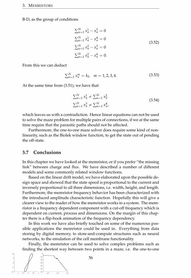
-1 -0.5 0 0.5 1-10
-5
0
5
10
10 4 10 6 10 8-60
-50
-40
-30
-20
-10
0
3. MEMRISTORS
B-D, as the group of conditions
řNn=1 x1
n ´ x3n = 0
řNn=1 x1
n ´ x4n = 0
řNn=1 x2
n ´ x3n = 0
řNn=1 x2
n ´ x4n = 0.
(3.52)
From this we can deduct
řNn=1 xm
n = k0 m = 1, 2, 3, 4. (3.53)
At the same time from (3.51), we have that
řNn=1 x1
n ‰řN
n=1 x2n
řNn=1 x3
n ‰řN
n=1 x4n,
(3.54)
which leaves us with a contradiction. Hence linear equations can not be usedto solve the maze problem for multiple pairs of connections, if we at the sametime require that the parasitic paths should not be affected.
Furthermore, the one-to-one maze solver does require some kind of non-linearity, such as the Biolek window function, to get the state out of pendingthe off-state.
3.7 Conclusions
In this chapter we have looked at the memristor, or if you prefer “the missinglink” between charge and flux. We have described a number of differentmodels and some commonly related window functions.
Based on the linear drift model, we have elaborated upon the possible de-sign space and showed that the state speed is proportional to the current andinversely proportional to all three dimensions, i.e. width, height, and length.Furthermore, the memristor frequency behavior has been characterized withthe introduced amplitude characteristic function. Hopefully this will give aclearer view to the reader of how the memristor works in a system. The mem-ristor is a frequency dependent component with a cut-off frequency which isdependent on current, process and dimensions. On the margin of this chap-ter there is a flip-book animation of the frequency dependency.
In this work we have also briefly touched on some of the numerous pos-sible applications the memristor could be used in. Everything from datastoring by digital memory, to store-and-compute structures such as neuralnetworks, to the emulation of the cell membrane functionality.
Finally, the memristor can be used to solve complex problems such asfinding the shortest way between two points in a maze, i.e. the one-to-one
56

3.7. Conclusions
problem. However, the linear model is not adequate to solve two simultane-ous one-to-one problems in the same maze, due to the parasitic paths. Thememristor is a tricky two-terminal frequency component, with great poten-tial for storing and computing.
57

-1 -0.5 0 0.5 1-10
-5
0
5
10
10 4 10 6 10 8-60
-50
-40
-30
-20
-10
0

Chapter 4Miscellaneous
Our brain consists of a huge number of neural cells (neurons) and they arethe reason you can think and reflect. Today, we can mimic some simplerneural and adapting systems. But the whole brain is still to be understood.
4.1 Introduction
You may sometime wonder; what is intelligence? There is no entirely obvi-ous or clear answer to that question, and neither are we going to answer ithere. But the most common explanation is something like this; Intelligenceis the ability to store and use information to predict future events (or at leastthe probability of the events).
According to that definition the computer that defeated Kasparov inchess, Deep Blue1, would be intelligent. Similar to the victorious computer(cluster), Watson would be considered intelligent. However, if you ask thosecomputers to solve another task, they would most probably perform poorly.They only excel in one task. Actually, even a control system for a missile mayappear to be intelligent in its hunt for a fleeing target [8].
As Dawkins brutally states, intelligence is a bi-product in the strive forthe genes to survive [8]. This is a rather sobering insight. Furthermore, aninterpretation of Dawkins [8] book could be; you are merely a survival ma-chine for a set of genes, that happens to assert the most stable configuration,given the context.
The human brain consists of neurons, each connected to other neighbor-ing neurons, but also to neurons far away.
As seen in Fig. 4.1 the main blocks of a neuron are: the soma, dendrites,axon, and axon terminal. The connection between neurons are electrochemi-cally in small gaps between the axon terminal and dendrites. The axon termi-nal transmits to the dendrites. The dendrites are located on the soma (body)of the neuron and all the signals from the dendrites are summarized overthe surface of the soma. If the sum of all signals are above a threshold at theaxon hillock, an action potential (a spike) travels along the axon to the axonterminal via other neurons. [25]
1www-03.ibm.com/ibm/history/ibm100/us/en/icons/deepblue/, accessed March 2016
59

-1 -0.5 0 0.5 1-10
-5
0
5
10
10 4 10 6 10 8-60
-50
-40
-30
-20
-10
0
4. MISCELLANEOUS
Figure 4.1: Basic topology and functions of a neuron. Input signals to theneuron are applied at the dendrites, where a chemical transfer signal (neu-rotransmitter) is converted to an electrical potential. All input potentials aresummarized over the soma. If the potential at the axon hillock is above athreshold, this causes a wave of potential (also known as a action potential)to propagate over the axon. Finally the propagating action potential reachesthe the axon terminals, where the electrical potential is converted to chemicaltransmitters to dendrites of other neurons or cells. The axon may be warpedby Schwann cells, which causes the action potential to jump between thenodes of Ranvier and thus propagates faster and more energy efficient.
During development of the brain, the network of neurons are formedopportunistically. The brain seams to be very resilient. Even if you kill somethousands of brain cells by a really wet night at the pub, you will be able tofunction to some extent the next day.
In this chapter we will look on some imitations of neural networks.
Purpose
The purpose is to get an understanding of how neural networks operate andtheir possible applications for electronic systems. Especially, if they are ap-plicable for self organization in ECA or similar structures.
Demarcation
This work touches the field of ANN and WSN, with no deeper mathematicalinvestigation in regards of, for instance, sets, stability and so on.
Chapter overview
In this chapter we will cover two different ANN examples, the restrictedBoltzmann machine (RBM) and the Markov chain network. Finally we willlook into an WSN example where a malicious radio tries to disturb our net-work.
60

4.2. Artificial neural networks
Background
Almost any time you discuss the topic of nature-inspired electronics or com-puting, the function and properties of the neuron will appear in the discus-sion. Most people would agree that the function of the human brain in somerespect is involved in the appearance of our intelligence. Hence, the field ofANN seams to be an obvious area to familiarize oneself with before trying tobuild intelligent electronic systems.
4.2 Artificial neural networks
Artificial neural networks (ANN) is one of the collective terms for mimickingthe behavior of neurons. The degree of detail differs a lot, all from simplebinary networks such as Hopper field networks [26] to ambitious full detailsimulations such as the Blue brain project [80]. In addition there is a lot ofresearch going on to understand the brain such as the Human brain project[81].
ANN can learn by regression of the data (to be learned). The update ofnetwork coefficients, i.e. the connection strength between the neurons, canbe done by many different methods, among them are the Hebbian learningand the delta rule.
Hebbian learning is based on biology and can be delightfully explainedby the famous experiment Pavlov did on dogs. In short, the experiment goeslike this. Dogs that see food, have an increased tendency to drool. Ringing abell in the presence of the dog without any food present, does not change itstendency to drool. However, if the bell rings, every time the dog sees food,there will be an association between food and the bell. Eventually, only thebell is enough to make the dog to have an increased tendency to drool. Ona neuronal level, the connection strength between neurons for drool and thebell are getting stronger in the simultaneous of exposure to food and bell.Eventually the bell neurons are enough to signal to the drool neuron. [26]
The delta rule simply uses the difference of what the ANN produces andthe expected correct result, i.e. the training data, and updates the connec-tion strengths in network by a quantity corresponding to a fraction of thedifference. [26]
ANN can be used in many different applications, in [82] the network isused for distance estimation in images of a stereoscopic feed of frames.
The image feed from each camera is processed one frame at the time witha set of electronic neurons. A sub-window is swept over the frame in bothhorizontal and vertical position. The image data from the sub-window isapplied to the neurons, which each and every one, calculate the sum of theabsolute distance between the input data and previously learned data.
The label of the neuron with the lowest sum, shows what have beenfound, and the position of the sub-window where it has been found. Theprocessing is done on both cameras frame and the difference in position isused to calculate the distance to the object.
61

-1 -0.5 0 0.5 1-10
-5
0
5
10
10 4 10 6 10 8-60
-50
-40
-30
-20
-10
0
4. MISCELLANEOUS
Figure 4.2: The structure of a restricted Boltzmann machine. The input datais presented at the visible nodes v0 : vn, which are connected to the hiddennodes h0 : hm by the connection matrix W.
Restricted Boltzmann machine
The connections and nodes in an restricted Boltzmann machine (RBM) areshown in Fig. 4.2. The RBM is a reduced form of the normal Boltzmannmachine. Connections are only allowed between visible and hidden nodes.No connections are present between any two hidden nodes or any two visiblenodes. [83]
The nodes vi and hi are binary and the connection matrix W is initial-ized with random numbers, preferably normal distributed with a varianceof about 0.01. Please note that v0 and h0 are constant ones, 1, to feature biasterms.
The connections between the visible nodes and hidden nodes are indirectby probability functions. The probability that the hidden node hi is set to oneat time instance k is given by
Pr(hki = 1) =
11 + exp(´
řnj=0 Wijvk
j ). (4.1)
And similarly, the probability of node vi to be set to one, 1, at time instancek + 1 is
Pr(vk+1j = 1) =
11 + exp(´
řmi=0 Wijhk
i ). (4.2)
A visualization of an execution of a RBM is shown in Fig. 4.3. At the firsttime instance, the input data is presented at the visible nodes. The infor-mation is then transferred via the connections to the hidden nodes. Fromthe hidden nodes, the information is transferred back to the visible nodes.
62

4.2. Artificial neural networks
Figure 4.3: The Boltzmann machine operates by using the input data to setthe visible nodes (v1
j ), and then generates the state of the hidden nodes (h1i ),
which in turn generate new visible nodes (v2j ) and so on. The movement of
data from the visible nodes to the hidden nodes and back again is called ashake and is done a predefined number of steps. At the end, the final shakepresents the result from the network, the belief.
The procedure of transferring information from the visible nodes to the hid-den and back again is called “a shake”. After a number of shakes the modelbelief can be found at the visible nodes. The number of shakes is a param-eter of appropriate design selection between one and infinity. Learning isdone by grouping data, in any order, into batches and update the connectionstrengths according to
∆Wi j =ă v1j h1
i ą ´ ă vqj hq
j ą (4.3)
andW = W + α∆W, (4.4)
where ă x ą denotes the mean of xn in a batch.The (4.3) can be seen as the difference between real data and what the
model “believes”. A common nomenclature is ∆Wi j =ă vjhi ądata´ ă vjhj ąmodel . Another common practice is to use the same variablefor visible and hidden nodes, that is ∆Wi j =ă sjsi ądata ´ ă sjsj ąmodel ,which is really confusing when entering the field. As seen, the RBM usesboth Hebbian learning and the delta rule.
From a biological point of view, the RBM is not plausible, since each pairof hidden and visible nodes uses the same weight (strength).
Simple vector recognition example
A restricted Boltzmann machine of 16 visible nodes and five hidden nodesis trained on four different symbols, as seen in Table 4.1, where each symbolhave all bits in a nibble group set to one. The restricted Boltzmann machine istrained in batches of 500 samples each in 1000 steps, which may have been alittle too extensive in retrospect. The trained RBM is then presented with data
63

-1 -0.5 0 0.5 1-10
-5
0
5
10
10 4 10 6 10 8-60
-50
-40
-30
-20
-10
0
4. MISCELLANEOUS
Nibbles v1 : v4 v5 : v8 v9 : v12 v13 : v16Vector1 1111 0000 0000 0000Vector2 0000 1111 0000 0000Vector3 0000 0000 1111 0000Vector4 0000 0000 0000 1111
Table 4.1: The training data for a restricted Boltzmann machine in the simplevector recognition example.
to reconstruct. In our example, all piece of presented data is reconstructed500 times and averaged. This may also have been a little too extensive. Thetraining data vectors, the vectors to reconstruct and the reconstructed vectorscan be found in Fig. 4.4, where each pixel column represents a vector. Thenetwork seems to reconstruct the missing data quite well.
Image reconstruction example
The restricted Boltzmann machine can also be used to store and reconstructimages. To provide information about location in the image to the networkof nodes, two sets of potentials are used; one set of 20 potentials for the x-direction and one set of another 20 potentials for the y-direction.
poti(x) =1
1 + exp(´k(x´ xi)). (4.5)
The parameter k determines the sharpness and xi the location of each po-tential. Image data and potentials are then associated together in one vector
data = [R][G][B][pot1(x) . . . potn(x)][pot1(y) . . . potn(y)]. (4.6)
Training of the network is done with the image seen in Fig. 4.5, which has thesize of 30 by 30 pixels, and is performed in 500 batches of 500 vectors each.Reconstruction is performed in 128 batches, each containing 40 data points.The reconstructed image can be found in Fig. 4.6, where fuzziness and minordeformation can be seen.
To get a neural network to learn and reconstruct data often requires somekind of tweaking and testing to get reasonable results. There is always someparameter that has to be adjusted.
In the example above, there is only one pixel associated with each inputvector. This can, quite possibly, be increased to include neighboring pixelsas well. But then, the initial values of the reconstructed image, must mostprobably be considered, i.e., initial the image is mid gray, to make sure ofproper converging.
Markov-lyrics
Let us assume that we have some kind of sequenced data of a specific kind,but there is not enough for our particular application. Hence, we would
64

4.2. Artificial neural networks
24
2468
10
12
14
16
Tra
in d
ata
24
2468
10
12
14
16
Test d
ata
510
15
20
2468
10
12
14
16
Reconstru
cte
d d
ata
510
15
20
2468
10
12
14
16
Trainingdata
TestdataR
econstructeddata
Figure 4.4: The training, test, and reconstructed data of a restricted Boltz-mann machine. Top: The training data, each pixel column represents onevector. Middle: The test data to be reconstructed. Bottom: The resultingreconstructed data according to test data and the knowledge stored in thenetwork.
65

-1 -0.5 0 0.5 1-10
-5
0
5
10
10 4 10 6 10 8-60
-50
-40
-30
-20
-10
0
4. MISCELLANEOUS
5 10 15 20 25 30
5
10
15
20
25
30
Figure 4.5: The original image which the neural network is trained on. Inaddition to the image data, two sets of potentials, depending on the pixellocation, are used to form the input vector.
like to find a method to generate more data with similar properties. Then aMarkov model could be of use.
From a set of data we train the model by looking at short, fixed size,pieces of data. The model assumes that the symbols before the last symbol(or so) implies which the last symbol can be in that piece, i.e., the last symbolin the piece correlates with the previous symbol in the piece. As seen in theexample in Fig. 4.7, looking at the piece “lo wo” in “Hello world” tells themodel that there is a probability of a ’o’ after the sequence “lo w”.
The next piece is generated by increasing n by one, and now the modellearns that there is an increased probability of having an ’r’ after “o wo”.
One way to implement this model is to use a tree structure as in Fig. 4.8.Each letter in the current piece points at a branch for each level. At the end,leaves counters keep track of the occurrence of the different symbols. Afterthe last piece has been presented to the model, each leaf can be assigned aprobability linear to the value of the counter of each leaf compared to thesum of all the counters of leaves in that subtree, or in mathematical terms
PrtSn = sn|Sn´1 = sn´1, ..., Sn´m = sn´mu. (4.7)
That is, given the sequence of previous symbols, what is the probability ofthe next symbol?
66

4.2. Artificial neural networks
5 10 15 20 25 30
5
10
15
20
25
30
Figure 4.6: A reconstructed image from the network. Given the two sets ofpotentials, in x-direction and y-direction, each pixel is reconstructed by therestricted Boltzmann machine to complete a image similar to the original inFig. 4.5
Figure 4.7: In the learning of the Markov model, a piece is selected from thedata and the occurrence of that particular symbol combination is learned.Then, another piece is selected and learned and so on.
67

-1 -0.5 0 0.5 1-10
-5
0
5
10
10 4 10 6 10 8-60
-50
-40
-30
-20
-10
0
4. MISCELLANEOUS
Figure 4.8: The Markov model can be seen as a structural tree, where thebranching is done on previous symbols in the piece. The leaves contains theprobabilities of the different symbols.
To generate data from the Markov tree, we need to start with an initialseed, which can be either the first symbols or any piece of the data learned, orany random path in the tree. The seed cannot be completely randomly gen-erated directly since there is nothing to guarantee that this particular symbolsequence exists in the model.
Given the seed, which is now pointing out a subtree, a new symbol isgenerated randomly given the different probabilities in that subtree, and thatsymbol is added to the output, as seen in Fig. 4.9.
To generate the next symbol, the last symbols of the output now pointsout another subtree which generates the next symbol. In this manner themodel can produce any desired amount of data.
The size of the pieces that the model work with determines how randomthe output will be compared to the input data of the model. If the modelwork with very short pieces there is not enough information to capture thebehavior of the data and the model only produces almost random noise. Ifthe piece length is too long, the subtrees becomes more deterministic, sinceonly one or a few leaves in the subtree has a probability higher than zero. Inthe absolute worst case, only the input data it self come out of the model.
As an example, we used a major part of the Swedish lyrics from the musicgroup Kent as input. The piece length was chosen to six letters, which gave
68

4.3. Wireless sensor networks
Figure 4.9: Generating output data from the Markov model. The last symbolspoint out a subtree of probabilities for the next symbol and a new symbol isgenerated, and the piece index is incremented to generate another symbol.
Figure 4.10: A small example of a wireless sensor network with ten motesand one base station.
a reasonable, i.e. readable, output with new fresh lyrics in similar style as ofthe original author, Joakim Berg. Unfortunately, Universal Music Sweden2
did object publication of the result. There seems to exist a legal gray area,somewhere between random letters and the original lyrics.
4.3 Wireless sensor networks
A WSN can be any network of sensors that is communicating wireless. How-ever, here we focus on a subset. Smart dust is the term for an WSN withphysical small nodes, also referred as motes, which are distributed in wastvolumes.
The motes are spread out over the area of interest, as seen in Fig. 4.10,where one base station collects the data from the network. The placementcan either be deliberate, at exact positions, or random. When the motes areplaced deliberately, the location of each mote can be specified exactly. Whenplacing the motes randomly, such as sprinkled from an air vessel, the loca-tions can not be determined and the network must therefore self organize itsstructure. The sprinkle technique should be an effective way to cover largeareas fast.
Each mote consist of at least four parts: Energy storage, signal re-ceiver/transmitter in any media (radio or laser) [84], one measurement
2www.universalmusic.se, accessed 2016-01-22
69

-1 -0.5 0 0.5 1-10
-5
0
5
10
10 4 10 6 10 8-60
-50
-40
-30
-20
-10
0
4. MISCELLANEOUS
Energy harvesterPiezoelectricPhotovoltaic
Chemical
CommunicationinterfaceRF, wired
Centralcontroller unit
Sensor interface
ADCSensor
precond.
Wake-upmechanisms
Energy storageSupercapBattery
Power mngmtRegulators
DC-DC conv.
Memory WSNmote
Figure 4.11: A system block diagram of a WSN mote. A mote must have atleast one function block in each category including: energy (green), commu-nication (blue), measurement (beige-orange), and control (gray).
equipment of some physical property of the environment, and some kindof decision circuit. In addition there may be one or more energy harvestingmodules and additional functions, for instance, for measurement and othermeans of communication. A system block diagram of a typical WSN motecan be found in Fig. 4.11.
The application fields for a mote network are probably many more thenwe can imagine, but suggested applications has been: surface explorationof other planets [85], drought warning, monitoring of NOx-concentrationsin crop fields, monitor the amount of pedestrians or animals in an area [86],border surveillance, finding missing/lost people in the woods and fire alarmover large woods.
The mote may behave differently depending on the available energy inthe storage and/or harvester. In the case where a lot of energy is availablethe mote can do more measurements, act more frequently as a relay stationfor messages from other motes and so on. In the case of low available energythe mote will be more restrictive in dispatching measurements and messages.All to sustain the network for as long as possible.
Since the network of motes is a swarm network solution, where any motemay sleep or be disconnected indefinitely (i.e. dead or stolen by thieves), theintelligence must originate from the network itself.
One way of creating intelligence is to reduce the information. The infor-mation reduction can be done by simple rules such as majority voting with acertain threshold. For instance, if a mote receives messages from three othermotes that there is a fire going on, it should start sending the message of fire.This will cause an avalanche of messages in the network and the informationwill soon reach the base station for further dispatch to the fire department.
A slightly more intelligent way of processing data would be to extractvirtual objects and send information of those instead. For instance, a front
70

4.3. Wireless sensor networks
of drought, which propagates trough the landscape, can be summarized bythe properties of location, speed, direction, and width. The motes clusterthemselves to one or many of those virtual objects and only one or a fewmessages are sent towards the base station.
Organization
So how should the network organize itself to arrange a messages to go to-wards the base station and how should one make sure that the motes closestto the base station do not suffer from energy depletion?
Well, for the organization part, the suggestion is what is called directeddiffusion [86, 87] or the waterfill model. The principle is very simple. Inan area with motes a base station broadcasts its presence with a zero, 0, levelidentification. All motes that manage to communicate in both directions withthe base station will acquire level 1. All motes that can communicate in bothdirection with motes on level 1, acquire level 2, and so on. For a mote net-work on a grid, with indices i and j, this can be expressed as
poti,j = minm=i+t´1,0,1u,n=j+t´1,0,1u(potm,n) + 1. (4.8)
Eventually all motes that can communicate, are attached to the network.Messages in the network will now flow, like water down the slope of lev-els, or directed by diffusion, towards the base station.
For a system designer of a such network, the hard question will be, howoften the network should reassign the level of each mote? This will be de-termined by the frequency of mote losses and the degree of overlap in theircommunication radii.
To reduce the total energy consumption in a WSN the motes in the net-work may be assigned different roles in a hierarchical substructure. For ex-ample as in [88, 89], the motes are gathered into small local clusters. In eachcluster there is one controlling mote that is handling all the routing. In as-sistance, there are relaying motes to communicate with controlling motes inother clusters. All other motes communicate only with the controlling motein the cluster. Since some motes in the cluster are doing more communi-cation than others, they may suffer from energy depletion, and then othermotes must step in and take over their role.
According to the classification in [90], the WSN described above is a selforganizing network (SON) with dynamic network protocol with multiplehop (multihop) communication.
In the work of [90], a small network is simulated in the programminglanguage Erlang. The communication protocol and behavior of each motewhere controlled by a finite state machine. In addition a energy model ofthe mote where also included. The work also acknowledge the major issueof limited energy available for each mote, in the range of a few Joules perday, compared to the energy needed to fulfill spectrum requirement in radiobroadcasting.
71

4. MISCELLANEOUS
Figure 4.12: A small wireless sensor network with two base stations. Themotes can have a potential to each base station and thus some spatial infor-mation can be deduced.
Networks with multiple base stations
With the water fill/directed diffusion approach, each mote will get an iden-tification by the levels to the base station. This identification also tells usa little bit about the geographical distance to the base station, assuming allmotes are similar and evenly distributed. By adding identification of the basestation and second base station at another location, as seen in Fig. 4.12 eachmote will have two address codes, one to each base station. This may bemapped to geographical points, if we assume that the motes are somewhatequally distributed over the area.
The additional base station also provides protection against hijacking ofthe network. For a single base station network, a hostile takeover can simplybe done by adding a malicious base station. This will rearrange the networkto send all messages to the false base station.
If the network contains two or more base stations and the motes sendmessages to them alternate or randomly, a malicious base station will onlypartly reduce the success rate of passing the information.
Equalization
In the simplest form of directed diffusion, no concern is taken to the energylevels of the battery of each mote. The algorithm is greedy and uses the short-est way to the sink, and hence the motes in the shortest path may die due todepletion of energy. A way to overcome this is to use the current availableenergy in each mote and select an appropriate alternative path, as suggested
72

4.3. Wireless sensor networks
by [91, 92] which they call aware adaptive directed diffusion (AADD). Theproblem with AADD is the need for central optimization.
Instead, the (4.8) can be adapted by considering the energy level availablein the mote
poti,j = minm=i+t´1,0,1u,n=j+t´1,0,1u(potm,n) + 1 + exp(
Emax ´ EλE
), (4.9)
where Emax is the maximum energy storage capacity, E the current energystored, and λE a design parameter.
By doing this, drained motes will be higher up in the diffusion potentialand the network will restructure to create other paths for the messages.
Another possible adaptation is to monitor the potential values of the moteneighbors, and try to adapt to be in the middle; similar to how birds and fishtry to be in the middle of their flock/shoal.
However, such mid way adaptation must have an adaptation gain lessthan one to ensure stability, for instance
poti,j = minm=i+t´1,0,1u,n=j+t´1,0,1u(potm,n) + 1 + exp(
Emax´EλE
)+
wři+1
m=i´1řj+1
n=j´1 potm,n/9,(4.10)
where w ăă 1.
Jamming of wireless sensor networks
As an implementation example we assume a quadratic field of one squarekm. The motes are placed in a 5 meters grid and the base station is placed asin Fig. 4.13. An interfering signal source, is also placed in the field, trying tojam the signals in the network.
The motes self organize according to directed diffusion by (4.8) and thedifferent potentials of the motes can be seen in Fig. 4.14. Motes close to thebase station or with low potential are denoted in black. Motes further awaywith high potential are denoted with white. The intermediate motes are de-noted with gray.
Link budget
To understand how a jamming source degrades on the signal between motes,we need to look at the energy in the link budget.
We make the following assumptions:
• The allowed frequency span is 2300-2450 MHz, and output power ofthe antenna is 1 mW.
• Each channel is 25 kHz wide.
• The distance between motes is 5 m, in grid pattern.
• Motes only communicate with its eight closest neighbors.
73

4. MISCELLANEOUS
Figure 4.13: Map location of the base station and the hostile jamming sourcein the field of motes.
• The jamming power is 200 W, spread through the whole spectrum.
The power into each receiver can be calculated by Friis’ equation [93, 94] by
Prx =PtxGtxGrx
Lbtr, (4.11)
where Ptx is the output power of the transmit amplifier, Gtx is the antennagain in transmitter and Grx is the receiver antenna gain. The propagationloss is calculated by
L =(4π)2
λ, (4.12)
where λ = c/ f .If we now look at the situation where one mote is transmitting to another
mote, while at the same time, the jamming source sends its signal, as seen inFig. 4.15. The revived power from the mote is
Pmote,in =Pmote,sentGtrGrt
Lmote,mote, (4.13)
while the transmitted power from the jamming source is
Pjam,in =Pjam,sentGjrGrj∆Ch
Ljam,mote∆B, (4.14)
74

4.3. Wireless sensor networks
Figure 4.14: Left: Organization example of a grid of motes. Each pixel repre-sents a mote and at the center left the sink is located. Right: Color encodingof potentials, from lowest (black) to highest (white).
where ∆B is the frequency bandwidth of the jamming source, and ∆Ch is thebandwidth of one channel. The mote only uses one of the available channels.
Assuming a bit error rate of 10´3 the signal to noise ratio should be about20 dB or higher [95], and therefore we set SNRmin = 20 dB. Now, similarto how the equalization consider stored energy, we may form an expressionthat consider the signal to noise conditions, that is
poti,j = minm=i+t´1,0,1u,n=j+t´1,0,1u(potm,n) + 1+
exp(´Pmote,in(dB)´Pjam,in(dB)´SNRmin
λSNR),
(4.15)
where λSNR determine the sharpness of the function and have to be chosenby the designer. The associated cost is the need for a signal to noise estima-tion in each mote.
In Fig. 4.16 the potentials of the motes in the network are shown. Thewhite circle is the motes the jamming source has managed to knock out ofthe network. The parameter λSNR has been set to 0.1, which gives a rathersharp and distinct transition between non-jammed and jammed motes. Wealso see in Fig. 4.16 how the network adapts and wraps around the jammedarea, at the cost of having the upper right corner motes at a higher potential.
75

4. MISCELLANEOUS
Figure 4.15: Setup to calculate Friis’ equations for the signals mote to moteand jamming source to mote.
Figure 4.16: Left: The network of motes is jammed by a hostile signal. Thejamming source can only disable motes within the region where it can in-terfere enough with the signals of neighboring motes (the white circle). Therest of the network realign itself. Right: Color encoding of potentials, fromlowest (black) to highest (white).
76

4.4. Conclusions
As seen above, a WSN, which uses directed diffusion, can adapt tochanges in the environment such as energy levels and as in the example,jamming of the network. The adaptation time does of course depend on thesize of the network and how often energy is spent on communicating thepotentials.
4.4 Conclusions
We have looked at some systems that mimic the behavior of neurons or neu-ral systems. There are many different types and applications for ANNs andwe have only looked at a few.
The RBM system can learn a pattern and reproduce it, even if there aresome errors in the input. Furthermore, the RBM system can be used togetherwith potentials to store organization of cells. We could use this, to organizethe cells of an ECA which implement the clay system of the redundant FIRfilter, described in chapter 2. Furthermore, the RBM is basically opportunisticsince the initial connection matrix is randomized.
A neural network with lowest sum neurons where applied in imagerecognition and distance estimation of stereoscopic image streams. Further-more, any ANN can be implemented with the memristors described in chap-ter 3, since a crossbar structure in principle is a connection matrix.
We have also seen how a Markov system can be used to mimic patterns insequential data such as lyrics. Although the produced lyrics can not be foundthe original lyrics, they appear to have the same pathos. The Markov systemoffers a simple way to generate abundant amount of data with a particularinherent property, for testing systems (like the WSN).
Finally, we have seen how a WSN system can self organize by simplerules and adapt to the given context, in our case a malicious radio broadcastaimed to jam the system. The system behaves like clay, since it consist ofwast degree of redundancy of unified building blocks, i,.e. the motes. Fur-thermore, each mote is nameless until engaged to the network and assigneda potential.
A mote can be seen as a neuron. A computing device that communi-cate with other neurons. Possibly can a mote simulate several neurons. Thenetwork can be formed opportunistically in the same way as the neuronsconnects described in thesis intro. Both ANN and WSN are redundant sys-tems of unified subsystems, i.e. clay, where losses of subsystems is not acatastrophic failure.
77


Chapter 5Discussion
The power laws discussed in the introduction will live on. Exactly how longMoore’s law will apply, only the future can tell. One thing is for sure, thecurrent form will end and something else will take over. The size of the atomsis a hard limit with today’s technologies. Development of electronics willcontinue, but in a different way. One way could be the one described in thisthesis. We may very well see self organizing cellular based structures thatcan cope with the errors induced by very small devices, which induces highdeviations and reliability issues to such extent that current error correctionstrategies are not possible.
First, such a cellular array structure has to be organized by any means.That can be done with the strategy laid out in chapter 1, with successivedivision of the array together with internal state machines inside each cell,and at least one potential gradient. Another way is to use a neural networkin each cell together with a higher number of potential gradients, such asdescribed in chapter 4. However, instead of determine the color, the desiredcell function at each location can be selected. One may also ponder the ideaof combining both methods.
Second, since there is an error probability, we have to use redundancy toensure sufficient functionality. As we saw in chapter 2, it is possible to designsimple mean voter systems that do perform, but not as excellent as a majorvoter system does.
Third, once the cell functionality is decided in the cellular array, they haveto find paths for communication among themselves. In chapter 3, we elab-orated on the possibility to use the memristor in solving a maze problem.That does work fine as long as there is only one path to be found. However,in real applications there is strong reason to believe that several paths have tobe solved simultaneously. There may be a way to do this, but here we didn’tfind it.
The memristor shows interesting properties. This device is frequency de-pendent for a fixed current amplitude. Since it is a two terminal device, boththe input and the output have to be applied to the same pins, which makesthe device tricky to use in circuits. However, the device does have great
79

5. DISCUSSION
potential to be the next memory solution, due to the small feature size andability to retain the content without power (non-volatile).
Beside the plasticity of the neural networks, we have also looked brieflyinto the plasticity of wireless sensor networks, where we saw the networkability to reshape and realign due to the context of the network and energysituation. Finally, the patos of Kent lyrics was captured in a Markov model,which where able to generate new lyrics.
The combined topics above may very well play part in the future devel-opment of electronics. So, Moore’s law will continue. However, the expo-nential growth of future systems will not mainly rely on the shrinkage ofthe transistors and other devices. Instead the growth will build on usageof abundance of subsystem, where the cost of each individual system is re-duced.
Future electronics will be like clay since it will be abundant and redun-dant, due to the error probability Unified cells may overtake each other place,like the smart dust WSN and somewhat the redundant FIR filter. Futureelectronics will be like clay since it will be opportunistic, adapting and plas-tic. Forming paths or adjusting strength in connections as the environmentchanges, both the internal environment, such as which nodes or PEs areworking, and the external environment, such as the available energy or theinput data or any possible competition for resources.
As errors occurs on the system, we will have a softly degrading systemand may have to accept loss in performance or accuracy.
The exact location of any function will be unknown to the designer, andthe organization will be autonomous based on any combination of potentials,neural networks, or sequencing schemes in the same way as egg turn into afetus. In fact, the transition to clay electronics has already started to someextent. Today’s super computer does have a clay like appearance from a pro-grammers perspective. The computer is built by a large number of smallercomputers, interchangeable to each other. The programmer does not knowexactly which computer is going to do which calculation, or which node isgoing to be the main node. All the programmer, or exerciser of the program,knows, is the number of nodes.
80

Bibliography
[1] Frank Benford. “The Law of Anomalous Numbers.” In: Proceedings ofthe American Philosophical Society 4 (1938), p. 551. ISSN: 0003049X.
[2] Mark J. Nigrini and Linda J. Mittermaier. “The Use of Benford’s Lawas an Aid in Analytical Procedures.” In: Auditing: A Journal of Practice& Theory 16.2 (1997), pp. 52 –67. ISSN: 02780380.
[3] J.S. Kilby. “Invention of the integrated circuit”. In: Electron Devices,IEEE Transactions on 23.7 (July 1976), pp. 648–654. ISSN: 0018-9383. DOI:10.1109/T-ED.1976.18467.
[4] Paul E. Ceruzzi. “Moore’s Law and Technological Determinism: Re-flections on the History of Technology.” In: Technology and Culture 3(2005), p. 584. ISSN: 0040165X.
[5] C. H. (Kees) van Berkel. “Multi-core for Mobile Phones”. In: Proceed-ings of the Conference on Design, Automation and Test in Europe. DATE’09. Nice, France: European Design and Automation Association, 2009,pp. 1260–1265. ISBN: 978-3-9810801-5-5.
[6] R. Want. “When Cell Phones Become Computers”. In: IEEE PervasiveComputing 8.2 (Apr. 2009), pp. 2–5. ISSN: 1536-1268. DOI: 10.1109/MPRV.2009.40.
[7] Jeff Hawkins and Sandra Blakeslee. On Intelligence. St. Martin’s Griffin,2004. ISBN: 0805074562.
[8] Richard Dawkins. The Selfish Gene. New York: Oxford University Press,1976.
[9] Bruce Alberts. Essential cell biology. New York : Garland Science, c2010,2010. ISBN: 9780815341291.
[10] Bruce Alberts. Molecular biology of the cell. New York : Taylor & Francis,cop. 2008, 2008. ISBN: 9780815341062.
[11] Dennis Bray. Wetware : a computer in every living cell. New Haven ; Lon-don : Yale University Press, c2009., 2009. ISBN: 9780300141733.
[12] R.K. Cavin, P. Lugli, and V.V. Zhirnov. “Science and Engineer-ing Beyond Moore’s Law”. In: Proceedings of the IEEE 100.SpecialCentennial Issue (May 2012), pp. 1720–1749. ISSN: 0018-9219. DOI:10.1109/JPROC.2012.2190155.
81

BIBLIOGRAPHY
[13] Susan J. Blackmore. Kort om medvetandet. Lidingö : Fri tanke, [2010],2010. ISBN: 9789186061067.
[14] G.E. Moore. “Cramming More Components Onto Integrated Circuits”.In: Proceedings of the IEEE 86.1 (Jan. 1998), pp. 82–85. ISSN: 0018-9219.DOI: 10.1109/JPROC.1998.658762.
[15] X. Tang, V.K. De, and J.D. Meindl. “Intrinsic MOSFET parameter fluc-tuations due to random dopant placement”. In: Very Large Scale Inte-gration (VLSI) Systems, IEEE Transactions on 5.4 (Dec. 1997), pp. 369–376. ISSN: 1063-8210. DOI: 10.1109/92.645063.
[16] A.J. Bhavnagarwala, X. Tang, and J.D. Meindl. “The impact of intrin-sic device fluctuations on CMOS SRAM cell stability”. In: Solid-StateCircuits, IEEE Journal of 36.4 (Apr. 2001), pp. 658–665. ISSN: 0018-9200.DOI: 10.1109/4.913744.
[17] H. Yamauchi. “A Discussion on SRAM Circuit Design Trend in DeeperNanometer-Scale Technologies”. In: Very Large Scale Integration (VLSI)Systems, IEEE Transactions on 18.5 (May 2010), pp. 763–774. ISSN: 1063-8210. DOI: 10.1109/TVLSI.2009.2016205.
[18] Jan M. Rabaey. “Design at the End of the Silicon Roadmap”. In: Proceed-ings of the 2005 Asia and South Pacific Design Automation Conference. ASP-DAC ’05. Shanghai, China: ACM, 2005, pp. 1–2. ISBN: 0-7803-8737-6.DOI: 10.1145/1120725.1120729.
[19] John von Neumann. “Probabilistic logics and the synthesis of reliableorganisms from unreliable components”. In: Automata studies 34 (1956),pp. 43–98.
[20] S. Mitra, N.R. Saxena, and E.J. McCluskey. “Common-mode failures inredundant VLSI systems: a survey”. In: Reliability, IEEE Transactions on49.3 (Sept. 2000), pp. 285–295. ISSN: 0018-9529. DOI: 10.1109/24.914545.
[21] J.H. Lala and R.E. Harper. “Architectural principles for safety-criticalreal-time applications”. In: Proceedings of the IEEE 82.1 (Jan. 1994),pp. 25–40. ISSN: 0018-9219. DOI: 10.1109/5.259424.
[22] W. Ibrahim, V. Beiu, and A. Beg. “Optimum Reliability Sizing for Com-plementary Metal Oxide Semiconductor Gates”. In: Reliability, IEEETransactions on 61.3 (Sept. 2012), pp. 675 –686. ISSN: 0018-9529. DOI:10.1109/TR.2012.2206249.
[23] R. Fuchsen. “IMA NextGen: A new technology for the Scarlett pro-gram”. In: Aerospace and Electronic Systems Magazine, IEEE 25.10 (Oct.2010), pp. 10–16. ISSN: 0885-8985. DOI: 10.1109/MAES.2010.5631720.
[24] ASHLEY Project Homepage. Accessed October 2011. URL: http://www.ashleyproject.eu/.
[25] Arthur C. Guyton and John E. Hall. Textbook of Medical Physiology.11th ed. Elsevier Saunders, 2006.
82

Bibliography
[26] Helge Malmgren. Inlärning och minne i neurala nätverk. 1:2. Studentlit-teratur, 2007.
[27] B. Parhami. “Voting networks”. In: Reliability, IEEE Transactions on 40.3(Aug. 1991), pp. 380–394. ISSN: 0018-9529. DOI: 10.1109/24.85461.
[28] E.P. Kim and N.R. Shanbhag. “Soft N-Modular Redundancy”. In: Com-puters, IEEE Transactions on 61.3 (Mar. 2012), pp. 323–336. ISSN: 0018-9340. DOI: 10.1109/TC.2010.253.
[29] S. Askari et al. “Scalable mean voter for fault-tolerant mixed-signal cir-cuits”. In: Aerospace Conference, 2010 IEEE. Mar. 2010, pp. 1–10. DOI:10.1109/AERO.2010.5446666.
[30] Leslie Lamport, Robert Shostak, and Marshall Pease. “The ByzantineGenerals Problem”. In: ACM Trans. Program. Lang. Syst. 4.3 (July 1982),pp. 382–401. ISSN: 0164-0925. DOI: 10.1145/357172.357176.
[31] Deb Kalyanmoy. Multi-Objective Optimization using Evolutionary Algo-rithms. Wiley, 2001.
[32] Claudio Mattiussi and Dario Floreano. “Analog Genetic Encoding forthe Evolution of Circuits and Networks”. In: Evolutionary Computation,IEEE Transactions on 11.5 (Oct. 2007), pp. 596–607.
[33] Kotha Srinivasa Reddy and Subhendu Kumar Sahoo. “An approachfor FIR filter coefficient optimization using differential evolution algo-rithm”. In: AEU - International Journal of Electronics and Communications69.1 (2015), pp. 101 –108. ISSN: 1434-8411. DOI: 10.1016/j.aeue.2014.07.019.
[34] Sangeeta Mandal et al. “Design of optimal linear phase FIR high passfilter using craziness based particle swarm optimization technique”.In: Journal of King Saud University - Computer and Information Sciences24.1 (2012), pp. 83 –92. ISSN: 1319-1578. DOI: 10.1016/j.jksuci.2011.10.007.
[35] J. Alvbrant and J.J. Wikner. “Study and simulation of an exampleredundant FIR filter”. In: NORCHIP, 2012. Nov. 2012, pp. 1–4. DOI:10.1109/NORCHP.2012.6403121.
[36] Lars Wanhammar. DIGITAL FILTERS. Linköping University, 2007.
[37] A. H. Land and A. G. Doig. “An automatic method of solving discreteprogramming problems.” In: Econometrica 28 (1960), pp. 497 –520.
[38] Omprakash K. Gupta and A. Ravindran. “BRANCH AND BOUNDEXPERIMENTS IN CONVEX NONLINEAR INTEGER PROGRAM-MING.” In: Management Science 31.12 (1985), pp. 1533 –1546. ISSN:00251909.
83

BIBLIOGRAPHY
[39] D. Dallet et al. “Dynamic testing of A/D converters: how many sam-ples for a given precision?” In: Instrumentation and Measurement Tech-nology Conference, 1996. IMTC-96. Conference Proceedings. Quality Mea-surements: The Indispensable Bridge between Theory and Reality., IEEE.Vol. 2. 1996, 1298 –1303 vol.2. DOI: 10.1109/IMTC.1996.507581.
[40] Lennart Ljung. System Identification, Theory for the user. Ed. by ThomasKailath. 2nd. Prentice Hall, 1999.
[41] L. Chua. “Memristor-The missing circuit element”. In: IEEE Transac-tions on Circuit Theory 18.5 (Sept. 1971), pp. 507 –519. ISSN: 0018-9324.DOI: 10.1109/TCT.1971.1083337.
[42] R. Williams. “How We Found The Missing Memristor”. In: IEEE Spec-trum 45.12 (2008), pp. 28–35. ISSN: 0018-9235. DOI: 10.1109/MSPEC.2008.4687366.
[43] Dmitri B. Strukov et al. “The missing memristor found”. In: Na-ture 453.7191 (May 2008), pp. 80–83. ISSN: 0028-0836. DOI: 10 . 1038/nature06932.
[44] Dmitri B. Strukov and R. Stanley Williams. “Four-dimensional addresstopology for circuits with stacked multilayer crossbar arrays”. In: Pro-ceedings of the National Academy of Sciences 106.48 (2009), pp. 20155–20158. DOI: 10.1073/pnas.0906949106.
[45] J. Alvbrant, V. Keshmiri, and J.J. Wikner. “Transfer characteristics andbandwidth limitation in a linear-drift memristor model”. In: CircuitTheory and Design (ECCTD), 2015 European Conference on. Aug. 2015,pp. 1–4. DOI: 10.1109/ECCTD.2015.7300037.
[46] Vahid Keshmiri. “A Study of the Memristor Models and Applications”.MA thesis. Linköping University, 2014.
[47] Y.N. Joglekar and S.J. Wolf. “The elusive memristor: properties of basicelectrical circuits”. In: European Journal of Physics 30 (Jan. 2009), pp. 661–683. DOI: 10.1088/0143-0807/30/4/001.
[48] Z. Biolek, D. Biolek, and V. Biolkova. “Spice model of memristor withnonlinear dopant drift”. In: Radioengineering 18.2 (June 2009), pp. 210–214.
[49] T. Prodromakis et al. “A Versatile Memristor Model With Non-linearDopant Kinetics”. In: IEEE Transactions on Electron Devices 58.9 (Sept.2011), pp. 3099–3105. DOI: 10.1109/TED.2011.2158004.
[50] S. Kvatinsky et al. “TEAM: ThrEshold Adaptive Memristor Model”.In: Circuits and Systems I: Regular Papers, IEEE Transactions on 60.1 (Jan.2013), pp. 211–221. ISSN: 1549-8328. DOI: 10.1109/TCSI.2012.2215714.
[51] O. Kavehei et al. “The Fourth Element: Characteristics, Modeling andElectromagnetic Theory of the Memristor”. In: Proceedings of the RoyalSociety 466.2120 (Aug. 2010), pp. 2175–2202. DOI: 10.1098/rspa.2009.0553.
84

Bibliography
[52] Matthew D. Pickett et al. “Switching dynamics in titanium dioxidememristive devices”. In: Journal of Applied Physics 106.7, 074508 (2009),DOI: 10.1063/1.3236506.
[53] S. Benderli and T.A. Wey. “On SPICE macromodelling of TiO2 mem-ristors”. In: Electronics Letters 45.7 (26 March 2009), pp. 377–379. ISSN:0013-5194. DOI: 10.1049/el.2009.3511.
[54] J. Joshua Yang et al. “Memristive switching mechanismfor metal/oxide/metal nanodevices”. In: Nature Nanotech-nology 3.7 (July 2008), pp. 429–433. ISSN: 1748-3387. DOI:10.1038/nnano.2008.160.
[55] D. Biolek, Z. Biolek, and V. Biolkova. “SPICE Modeling of Memristive,Memcapacitative and Meminductive Systems”. In: Circuit Theory andDesign, 2009. ECCTD 2009. European Conference on. 23-27 August 2009,pp. 249–252. DOI: 10.1109/ECCTD.2009.5274934.
[56] E. Lehtonen and M. Laiho. “CNN using memristors for neighbor-hood connections”. In: Cellular Nanoscale Networks and Their Applica-tions (CNNA), 2010 12th International Workshop on. Feb. 2010, pp. 1–4.DOI: 10.1109/CNNA.2010.5430304.
[57] Dmitri B Strukov and Konstantin K Likharev. “CMOL FPGA: a re-configurable architecture for hybrid digital circuits with two-terminalnanodevices”. In: Nanotechnology 16.6 (2005), p. 888. URL: http ://stacks.iop.org/0957-4484/16/i=6/a=045.
[58] Changjian Gao and D. Hammerstrom. “Cortical Models Onto CMOLand CMOS – Architectures and Performance/Price”. In: Circuits andSystems I: Regular Papers, IEEE Transactions on 54.11 (Nov. 2007),pp. 2502–2515. DOI: 10.1109/TCSI.2007.907830.
[59] David K. Cheng. Field and Wave Electromagnetics. Ed. by Babara Rifkind.2nd Edition. Addison-Wesley Publishing Company, Inc, 1989.
[60] H. Abdalla and M.D. Pickett. “SPICE modeling of memristors”. In: Cir-cuits and Systems (ISCAS), 2011 IEEE International Symposium on. May2011, pp. 1832–1835. DOI: 10.1109/ISCAS.2011.5937942.
[61] S. Kvatinsky et al. Verilog-A for Memristors Models. Tech. rep. 801. CCITTechnical Report, Dec. 2011.
[62] P. Mazumder, S.M. Kang, and R. Waser. “Memristors: Devices, Models,and Applications [Scanning the Issue]”. In: Proceedings of the IEEE 100.6(June 2012), pp. 1911–1919. ISSN: 0018-9219. DOI: 10.1109/JPROC.2012.2190812.
[63] E. Lehtonen and M. Laiho. “Stateful implication logic with memris-tors”. In: Nanoscale Architectures, 2009. NANOARCH ’09. IEEE/ACMInternational Symposium on. July 2009, pp. 33–36. DOI: 10 . 1109/NANOARCH.2009.5226356.
85

BIBLIOGRAPHY
[64] Julien Borghetti et al. “‘Memristive’ switches enable ‘stateful’ logicoperations via material implication”. In: Nature (Apr. 2010). DOI:10.1038/nature08940.
[65] S. Kvatinsky et al. “The Desired Memristor for Circuit Designers”. In:Circuits and Systems Magazine, IEEE 13.2 (Secondquarter 2013), pp. 17–22. ISSN: 1531-636X. DOI: 10.1109/MCAS.2013.2256257.
[66] Warren Robinett et al. “A memristor-based nonvolatile latch circuit”.In: Nanotechnology 21.23 (2010), p. 235203. URL: http://stacks.iop.org/0957-4484/21/i=23/a=235203.
[67] Yuriy V. Pershin and Massimiliano Di Ventra. “Practical approach toprogrammable analog circuits with memristors.” In: (2009).
[68] T. W. Lee and J. H. Nickel. “Memristor Resistance Modulation for Ana-log Applications”. In: IEEE Electron Device Letters 33.10 (21 September2012), pp. 1456–1458. DOI: 10.1109/LED.2012.2207429.
[69] A. L. Hodgkin and A. F. Huxley. “A quantitative description of mem-brane current and its application to conduction and excitation innerve”. In: The Journal of Physiology 117.4 (1952), pp. 500–544. ISSN:1469-7793. DOI: 10.1113/jphysiol.1952.sp004764.
[70] S. Alam and S.M. Rezaul Hasan. “Modelling of calcium ion (Ca+2) con-ductance in nerve membrane protein channel as memristive circuit el-ement”. In: Electronics Letters 47.25 (Dec. 2011), pp. 1361–1363. ISSN:0013-5194. DOI: 10.1049/el.2011.3332.
[71] M.P. Sah, Hyongsuk Kim, and L.O. Chua. “Brains Are Made of Mem-ristors”. In: Circuits and Systems Magazine, IEEE 14.1 (stquarter 2014),pp. 12–36. ISSN: 1531-636X. DOI: 10.1109/MCAS.2013.2296414.
[72] Omid Kavehei. “Memristive devices and circuits for computing, mem-ory, and neuromorphic applications”. PhD thesis. School of Electricaland Electronic Engineering, 2012. URL: http://hdl.handle.net/2440/73316.
[73] M. Versace and B. Chandler. “The brain of a new machine”. In:Spectrum, IEEE 47.12 (Dec. 2010), pp. 30–37. ISSN: 0018-9235. DOI:10.1109/MSPEC.2010.5644776.
[74] G. Howard et al. “Evolution of Plastic Learning in Spiking Net-works via Memristive Connections”. In: Evolutionary Computation,IEEE Transactions on 16.5 (2012), pp. 711–729. ISSN: 1089-778X. DOI:10.1109/TEVC.2011.2170199.
[75] S.P. Adhikari et al. “Memristor Bridge Synapse-Based Neural Net-work and Its Learning”. In: Neural Networks and Learning Systems,IEEE Transactions on 23.9 (2012), pp. 1426–1435. ISSN: 2162-237X. DOI:10.1109/TNNLS.2012.2204770.
[76] Snider. “Architecture and mmethod for computing with Reconfig-urable resistor crossbars”. 7,203,789 B2. 2007.
86

Bibliography
[77] Yuriy V. Pershin and Massimiliano Di Ventra. “Solving mazes withmemristors: A massively parallel approach”. In: PHYSICAL REVIEWE 84. American Physical Society, 2011.
[78] Massimiliano Di Ventra and Yuriy V. Pershin. “Fast computation withmemory circuit elements”. In: Cellular Nanoscale Networks and Their Ap-plications (CNNA), 2012 13th International Workshop on. Aug. 2012, pp. 1–3. DOI: 10.1109/CNNA.2012.6331429.
[79] I. Vourkas, D. Stathis, and G.Ch. Sirakoulis. “Massively Parallel AnalogComputing: Ariadne’s Thread Was Made of Memristors”. In: EmergingTopics in Computing, IEEE Transactions on PP.99 (2015), pp. 1–1. ISSN:2168-6750. DOI: 10.1109/TETC.2015.2420353.
[80] Henry Markram. “The Blue Brain Project”. In: Nat Rev Neurosci (2006),pp. 153–160. DOI: 10.1038/nrn1848.
[81] Eric R. Kandel et al. “Neuroscience thinks big (and collaboratively)”.In: Nat Rev Neurosci 9 (Sept. 2013), pp. 659–664. DOI: 10.1038/nrn3578.
[82] Lukas Vik and Fredrik Svensson. “Real-time stereoscopic object track-ing on FPGA using neural networks”. MA thesis. Linköping Univer-sity, Department of Electrical Engineering, 2014, p. 93.
[83] Geoffrey E. Hinton, Simon Osindero, and Teh Yee-Whye. “A FastLearning Algorithm for Deep Belief Nets.” In: Neural Computation 18.7(2006), pp. 1527 –1554. ISSN: 08997667.
[84] J. M. Kahn, R. H. Katz, and K. S. J. Pister. “Next Century Challenges:Mobile Networking for &Ldquo;Smart Dust&Rdquo;” in: Proceedingsof the 5th Annual ACM/IEEE International Conference on Mobile Comput-ing and Networking. MobiCom ’99. Seattle, Washington, USA: ACM,1999, pp. 271–278. ISBN: 1-58113-142-9. DOI: 10.1145/313451.313558.
[85] Philippe Dubois et al. “Ad hoc wireless sensor networks for explo-ration of Solar-system bodies.” In: Acta Astronautica 64 (2009), pp. 626–643. ISSN: 0094-5765.
[86] Chalermek Intanagonwiwat, Ramesh Govindan, and Deborah Estrin.“Directed Diffusion: A Scalable and Robust Communication Paradigmfor Sensor Networks”. In: Proceedings of the 6th Annual InternationalConference on Mobile Computing and Networking. MobiCom ’00. Boston,Massachusetts, USA: ACM, 2000, pp. 56–67. ISBN: 1-58113-197-6. DOI:10.1145/345910.345920.
[87] Chalermek Intanagonwiwat et al. “Directed Diffusion for Wireless Sen-sor Networking”. In: IEEE/ACM TRANSACTIONS ON NETWORKING11.1 (Feb. 2003), pp. 2–16.
87

BIBLIOGRAPHY
[88] Jielei Yu and Huazhong Zhang. “Directed diffusion based on cluster-ing and inquiry for wireless sensor networks”. In: Computer Science andInformation Technology (ICCSIT), 2010 3rd IEEE International Conferenceon. Vol. 2. July 2010, pp. 291–294. DOI: 10.1109/ICCSIT.2010.5564153.
[89] Prateek Sharma. “A study on a smart dust network and an analog in-terface”. MA thesis. Linköping University, Electronics System, 2012,p. 83.
[90] Maryam Abrishami. “A Study on Smart Dust Networks”. To be pub-lished. Master thesis. Linköping University, Feb. 2016.
[91] Jisul Choe and Kim Keecheon. “EADD: Energy Aware Directed Diffu-sion for Wireless Sensor Networks”. In: Parallel and Distributed Process-ing with Applications, 2008. ISPA ’08. International Symposium on. Dec.2008, pp. 779–783. DOI: 10.1109/ISPA.2008.104.
[92] Hao Qi, Fubao Wang, and Bingxiang Wang. “Energy aware adaptivedirected diffusion algorithm of wireless sensor networks”. In: Com-puter Science and Service System (CSSS), 2011 International Conference on.June 2011, pp. 385–388. DOI: 10.1109/CSSS.2011.5972028.
[93] Simon S. Haykin and Michael Moher. Modern wireless communications.Upper Saddle River, NJ : Pearson Prentice Hall, cop. 2005, 2005. ISBN:0130224723.
[94] C. Siva Ram Murthy and B. S. Manoj. Ad Hoc wireless networks : archi-tectures and protocols. Prentice Hall communications engineering andemerging technologies series. Upper Saddle River, NJ : Prentice Hall,cop. 2004, 2004. ISBN: 013147023X.
[95] R. Steel. Mobile Radio Communications. IEEE Press, 1992.
88

Avdelning, InstitutionDivision, Department
DatumDate
Språk
Language
l Svenska/Swedish
l Engelska/English
l
RapporttypReport category
l Licentiatavhandling
l Examensarbete
l C-uppsats
l D-uppsats
l Övrig rapport
l
URL för elektronisk version
ISBN
ISRN
Serietitel och serienummerTitle of series, numbering
ISSN
Linköping Studies in Science and Technology
Thesis No. 1745
TitelTitle
FörfattareAuthor
SammanfattningAbstract
NyckelordKeywords
Moore’s law has until today mostly relied on shrinkage of the size of the devices inintegrated circuits. However, soon the granularity of the atoms will set a limit togetherwith increased error probability of the devices. How can Moore’s law continue in thefuture? To overcome the increased error rate, we need to introduce redundancy. Applyingmethods from biology may be a way forward, using some of the strategies that transformsan egg into a fetus, but with electronic cells.
A redundant system is less sensitive to failing components. We define electronic clayas a massive redundancy system of interchangeable and unified subsystems. We showhow a mean voter, which is simpler than a majority voter, impact a redundant systemand how optimization can be formalized to minimize the impact of failing subsystems.The performance at given yield can be estimated with a first order model, without theneed for Monte-Carlo simulations. The methods are applied and verified on a redundantfinite-impulse response filter.
The elementary circuit behavior of the memristor, ”the missing circuit element”, is in-vestigated for fundamental understanding and how it can be used in applications. Dif-ferent available simulation models are presented and the linear drift model is simulatedwith Joglekar-Wolf and Biolek window functions. Driven by a sinusoidal current, thememristor is a frequency dependent component with a cut-off frequency. The memristorcan be densely packed and used in structures that both stores and compute in the samecircuit, as neurons do. Surrounding circuit has to affect (write) and react (read) to thememristor with the same two terminals.
We looked at artificial neural network for pattern recognition, but also for self organi-zation in electronic cell array. Finally we look at wireless sensor network and how suchsystem can adopt to the environment. This is also a massive redundant clay-like system.
Future electronic systems will be massively redundant and adaptive. Moore’s law willcontinue, not based on shrinking device sizes, but on cheaper, numerous, unified andinterchangeable subsystems.
EKS,Electrical Engineering581 83 Linköping
2016-04-18
978-91-7685-787-8
LIU-Tek-Lic--2016:1745
0280-7971
http://urn.kb.se/resolve?urn=urn:nbn:se:liu:diva-126333/
A study on emerging electronics for systems accepting soft errors
Joakim Alvbrant
ˆ
ˆ
Electronic clay, Redundant systems, Memristor, Wireless sensor net-works
