a thesis submitted for the degree of phd at the university...
TRANSCRIPT

University of Warwick institutional repository: http://go.warwick.ac.uk/wrap
A Thesis Submitted for the Degree of PhD at the University of Warwick
http://go.warwick.ac.uk/wrap/3639
This thesis is made available online and is protected by original copyright.
Please scroll down to view the document itself.
Please refer to the repository record for this item for information to help you tocite it. Our policy information is available from the repository home page.

ULTRA LOW ENERGY GOLD CLUSTER ION
BEAMS FOR SIMS APPLICATIONS
JUI-HSIEN CHANG MSc
Thesis for the degree of Doctor of Philosophy
submitted to
The University of Warwick
Department of Physics
August 2008
i

Table of Contents
Title Page…………………………………………………………………………i
Table of Contents………………………………………………………………..ii
List of Figures…………………………………………………………………...v
List of Tables…………………………………………………………………...xii
Acknowledgements……………………………………………………………xiii
Declaration…………………………………………………………………….xiv
List of Publications………………………………………………………….....xv
Abstract………………………………………………………………………..xvi
Chapter 1 Introduction…………………………………………………………1
1.1 Rationale………………………………………………………….1
1.2 Thesis overview…………………………………………………..2
Chapter 2 Secondary Ion Mass Spectrometry and Cluster Ion Effects..........4
2.1 Secondary ion mass spectrometry………………………………..4
2.1.1 Overview…………………………………………………4
2.1.2 Primary ion-solid interaction……………………………..5
2.1.2.1 Sputtering…………………………………………5
2.1.2.2 Secondary ion emission…………………………..7
2.1.2.3 The altered layer and depth profiling…………….9
2.1.3 SIMS instrumentation…………………………………...11
2.1.3.1 Overview………………………………………..11
2.1.3.2 Ion guns…………………………………………13
2.1.3.3 Double focussing magnetic sector………………15
2.1.3.4 Time-of-flight mass spectrometer………………17
2.1.3.5 Quadrupole mass spectrometer………………….19
2.2 Cluster SIMS and cluster ion sources….......................................23
2.2.1 Review of cluster ion bombardment…………………….23
2.2.2 Cluster ion sources developed for SIMS analysis of
semiconductors and metals……………………………...26
2.2.2.1 SFn+ (n = 1-5) and F– ion source…………….......26
2.2.2.2 Cn– (n = 4-10) and CsCn
– (n = 2-8) ion source….29
ii

2.2.2.3 Large gas cluster ion source…………………….29
2.2.2.4 C60+ ion source…………………………………..30
2.2.2.5 Aun– (n = 1-3, 5) ion source……………………..30
2.2.3 Silicon bombarded by gold ions………………………...31
Chapter 3 The Instrument and Ion Source – Overview….………………….35
3.1 EVA 2000……………………………………………………….35
3.2 Floating low energy ion gun (FLIG)……………………………40
3.3 The sputter cluster ion source (SCIS)…………………………...45
3.3.1 The set-up……………………………………………….45
3.3.1.1 The Cs+ emission system………………………..48
3.3.1.2 The sputter cone…………………………………50
3.3.2 The principles of operation……………………………...51
3.3.3 History of the source development and previous study…51
3.3.3.1 The prototype source……………………………52
3.3.3.2 The SCIS………………………………………...53
Chapter 4 Simulations and Retrofitting of the SCIS to the FLIG………….54
4.1 Space charge…………………………………………………….55
4.2 The simulation of ion emission and space charge………………57
4.2.1 Experimental………………………………………….....57
4.2.2 Aun– ion emission ………………………………………62
4.2.3 Space charge – comparison of SIMION simulation
and El-Kareh and El-Kareh’s theory …………………...65
4.2.4 The simulation of space charge in SCIS-FLIG…………66
4.3 The retrofit of the SCIS to the FLIG……………………………69
4.3.1 An additional lensing electrode and manifolds…………69
4.3.2 Mass separator (Wien filter)…………………………….72
4.3.3 The design of the electrical scheme……………………..75
Chapter 5 Improvements and Characterisations of SCIS-FLIG…..............79
5.1 The defects and improvements of the source…………………...79
5.1.1 Arcing and current leakage……………………………...79
5.1.2 Filaments issues…………………………………………81
5.1.3 Issues related to power supply units…………………….84
5.1.3.1 Inadequate sourcing and sinking currents………84
5.1.3.2 Heat dissipation…………………………………86
iii

5.1.4 Low vacuum and leakage……………………………….86
5.2 Characterisations of 1 keV Aun– ion beams……………………..88
5.2.1 Experimental…………………………………………….88
5.2.2 Mass spectra……………………………….....................88
5.2.3 Beam profile and transmission at the variable aperture...91
5.2.4 Spot size and current density……………………………93
5.2.5 Stabilisation and lifetime………………………………..94
5.2.6 The effective emission area……………………………..96
5.2.7 Gold ion yield ratio v.s. caesium sputter energy………..98
5.2.8 Space charge……….…………………………………....99
5.3 Higher energy and positive ions……………………………….101
5.4 New emission system………………………………………….102
Chapter 6 Gold Ion Bombardment………………………………………….108
6.1 Experimental…………………………………………………...108
6.2 Gold deposition and bombarded crater evolution ……………..109
6.3 Nonlinear sputtering by ultra-low energy Aun– ions…………..113
6.4 Surface topography…………………………………………….114
Chapter 7 Conclusions and Further Work.………………………………...117
7.1 Conclusions……………………………………………………117
7.2 Further improvements for the SCIS……………………………118
7.2.1 For the current design………………………………….118
7.2.1.1 Insulators………………………………………118
7.2.1.2 Filaments………………………………………120
7.2.2 New source…………………………………………….121
7.2.2.1 Reversed cone………………………………….121
7.2.2.2 Gold rod………………………………………..125
References……………………………………………………………………..128
iv

List of Figures
Fig. 2.1.1 Collision cascade and the occurrence of sputtering. The bombardment
of primary ions cause sample lattice atom displacements, sputtering and
primary ion deposition.
Fig. 2.1.2 The cosine angular distribution of Cu atoms sputtered by 20 keV
monomer Ar+ ions at normal incidence corresponds to Sigmund’s theory,
in contrast to that by 10 keV and 20 keV Ar2000 cluster ions. (reproduced
from Yamada I et al., 2001)
Fig. 2.1.3 Sputter yield and useful ion yield as a function of the primary beam
incidence angle (reproduced from Smith N S, 1996).
Fig. 2.1.4 Depth profile of a 1 nm think 30Si layer in 28Si. True position of the
layer is at 55.8 nm (reproduced from Smith N S, 1996).
Fig. 2.1.5 Schematic diagram of a double focus magnetic sector. Ions with a
mass, m, and an energy, E, emitted from the object at S1 are imaged at S2
by the electrostatic sector, and then S3 by the magnetic sector. Ions with
the same m but a different energy, E+ΔE, are corrected and focussed into
the same line.
Fig. 2.1.6 Schematic diagram of a TOF SIMS with a reflection analyser.
Secondary ions are reflected in the reflectron for energy compensation
and time discerned by a detector.
Fig. 2.1.7 Schematic diagram of quadrupole mass spectrometer. Two pairs of
cylindrical electrodes are applied a potential V but with opposite polarity.
Fig. 2.2.1 Yield enhancement due to cluster ion bombardment increases with
secondary ion nuclearity (reproduced from Belykh S F et al., 2001).
Secondary Sin+ ions were sputtered by Aum
– projectiles with E0 = 9 keV.
The K2,1 shown in the figure is the K2 as defined in Eqn. 2.2.1.
Fig. 2.2.2 Mechanical drawing of the hot filament duoplasmatron ion source
modified for operation as a triplasmatron (reproduced from Gillen G et al.
1999). The SF6 gas was fed through the Gas Feed #2 as indicated into
the pinch region, and the Gas Feed #3 into the expansion cup. The scale
was not specified in the paper, but should be in inch as is commonly used
in the U.S.
v

Fig. 2.2.3 Depth profiles of a Pd/Ti/SiO2/Si film by F– ions (reproduced from
Gillen G et al. 1999).
Fig. 2.2.4 Schematic diagram of the low energy focussed ion beam direct
deposition apparatus developed by Nagamachi et al. (reproduced from
Nagamachi et al. 1993). No neutral dump is shown, nor described in the
paper.
Fig. 3.1.1 The EVA 2000 SIMS instrument.
Fig. 3.1.2 Schematic diagram of the EVA 2000 vacuum system.
Fig. 3.1.3 Schematic diagram of the four degrees of freedom, namely x , ,
and , that the stage can be controlled, on which the sample holder
(Fig. 3.1.4) is fixed.
ˆ y z
θ
Fig. 3.1.4 Schematic diagram of two sample holders: one with a rectangular hole
of 700 μm×700 μm through it, another with a circular hole of Ø100 μm.
Fig. 3.1.5 The cross-sectional view of the designed Faraday cup mounted on the
EVA 2000 sample stage. (dimension shown in mm)
Fig. 3.2.1 Schematic diagram of the FLIG. Explanations are given in the text.
Fig. 3.2.2 Chromatic aberration and the disc of least confusion, Δrc. P and θ are
the principle plane and ray angle in the object space respectively, and P'
and θ' the counterparts in the image space.
Fig. 3.2.3 Geometrical optics showing lateral magnification. P and F are the
principal and focal planes in the object space, respectively, with a
refractive index n; P', F' and n' are the counterparts in the image space.
Fig. 3.2.4 The FLIG (only upper column) fitted with the SCIS on EVA 2000.
Fig. 3.3.1 The SCIS assembly as designed to fit onto a CAMECA IMS 4f SIMS
instrument in the University of Antwerp, Belgium.
Fig. 3.3.2 Orthographic cut-away projection of the SCIS assembly, after the
modifications had been made for its fitting with the FLIG. The numbers
are referred to Table 3.3.1.
Fig. 3.3.3 Schematic diagram of the Cs emission system.
Fig. 3.3.4 The Cs+ gun assembly as built in Antwerp University and subsequently
modified at Warwick. The numbers are referred to Table 3.3.1.
Fig. 3.3.5 Orthographic projection of the sputter cone.
vi

Fig. 4.1.1 The view of the cross section of a circular beam symmetrical about
the - axis. The beam has a radius of ri when leaving the focussing
electrode, and should be focussed at a distance di if space charge does not
exist. Due to space charge the beam reaches its minimum beam waist
(radius), rm, at a distance of dm from the electrode.
Fig. 4.2.1 (a) the Au cone, the cone entrance, the cone aperture and the five
emission areas. (b) The orthographic projection: ions are emitted from
the cone surface in the and yxˆˆ )ˆ(ˆ yx − planes. (c) The definition of Aun–
ions. There are 8 ray cones, and each ray cone has 24 equispaced rays,
making a total of 192 rays from an emission point.
Fig. 4.2.2 Schematic diagram of the beam design for SIMION space charge
effect simulations (in mm).
Fig. 4.2.3 Emission from the 1st area of the cone.
Fig. 4.2.4 Emission from the 3rd area of the cone.
Fig. 4.2.5 The transmission and the cross-over diameter of the 5 emission areas.
The errors for the transmission and the diameter are <0.01% and
± 0.004 mm respectively.
Fig. 4.2.6 Comparisons of beam waist position and radius between SIMION simulation and analytical calculations using the method of El-Kareh and
El-Kareh. Errors are given in the text.
Fig. 4.2.7 Simulations of space charge of the SCIS-FLIG: (a) 10 nA Au3–, (b)
100 nA Au3–, (c) 10 nA Au3
– (blue rays) with the secondary electrons (red
rays) deflected by the additional magnetic field.
Fig. 4.3.1 The simulation of an Au3– ion beam transmitting through the FLIG
column and the designed additional lensing electrode.
Fig. 4.3.2 Orthographic projection of the additional lensing electrode.
Fig. 4.3.3 The manifolds designed to retrofit the SCIS onto the FLIG.
Fig. 4.3.4 Schematic diagram of the Wien filter used for mass separation. (Note
in the FLIG, all electrodes of the Wien filter are floated.)
Fig. 4.3.5 (a) The newly designed outer magnetic circuit for the Wien filter to
separate gold ions. (b) Schematic diagram of the cross-sectional view of
the designed Wien filter (Fig. 3.2.4), including both the electric and
vii

magnetic parts. The magnetic part consists of the inner and outer circuits,
which make changing the magnetic field inside the FLIG easier.
Fig. 4.3.6 Schematic diagram of the SCIS electrical scheme.
Fig. 5.1.1 Arcing was observed between the connectors (linking the wires to the
feedthrough pins) when the source was tested for the first time. The
connectors were put in PTFE tubes and the arcing prevented. Also shown
is one of the badly welded areas that gave rise to vacuum leakage (section
5.1.4). The used insulator Alumina (Al2O3) changed to aluminium (Al)
when the oxygen was taken away by the deposited Cs atoms, which
resulted in electricity leakage.
Fig. 5.1.2 The ioniser filament was found to easily short to itself (a), and the
surrounding electrodes (b), when it was heated up for the first time. The
ceramics in between the filament supports and the plate which fixes the
supports were found covered by metallic materials that the insulating
properties stopped (b). (referred to Fig. 3.3.1 and 3.3.2)
Fig. 5.1.3 Simulation of the electron trajectories emitted from the ioniser filament.
The electrons emitted from the ioniser filament are attracted to the Cs+
ion extractor when the extractor potential is more positive than that of the
filament. This limits the controllability of the extractor potential, and thus
the Cs+ ion trajectories. All the electrode potentials in (b) are the same as
in (a) except that of the extractor is 100 volts more.
Fig. 5.1.4 The designed screen to prevent the electrons emitted from the ioniser
filament from being attracted to the Cs+ ion extractor. The device was
found to short with the extractor or the filament easily (dotted circled area)
when the source was hot.
Fig. 5.1.5 Schematic diagram of the trajectories of the charged particles
generated in the SCIS.
Fig. 5.1.6 Circuitry showing that the output voltage of a PSU, VOUT, is influenced
by its output impedance RS, the sourcing current, ISO, and the sinking
current, ISI.
Fig. 5.2.1 The normalised ion mass spectra, measured at the variable aperture
(VF = +0.018 kV) and at the Faraday cup (VF = +4.7 kV). The detected
monomer, dimmer and trimmer ion species were proved to be of gold.
viii

No other species can be observed. The error was in the range of 2.8 × 10–
3 % to 2.8 × 10⁻¹ %.
Fig. 5.2.2 The mass spectra measured at the Faraday cup at the sample position
when the controllability of all PSU had been established. The species
with 158 Da might be 158(CrCl3), 160(Fe2O3), 162.5(FeCl3), or a
combination of them.
Fig. 5.2.3 The Au1– beam profile at the variable aperture position when the lens
was tuned to obtain the highest transmission through the variable aperture
of Ø 800μm.
Fig. 5.2.4 An Au1– beam profile (normalised) when being scanned across a
rectangular hole (700×700 μm2) for determining the spot size at the
sample position. The current was about 0.4 nA.
Fig. 5.2.5 A mass spectrum measured at the sample when some parts of the gold
film had been exhausted due to sputtering. The peak of 179 Da should be
due to the addition of signals of 197Au1– and 158(CrCl3)–/160(Fe2O3)–/
162.5(FeCl3)–.
Fig. 5.2.6 Inspection of the cone after observation of impurity ions in the beam.
The cone was mainly sputtered at the aperture area, where steel is visible.
The entrance area was deposited with insulating materials.
Fig. 5.2.7 The simulation of ion emission when the experimental values of
electrical potentials are applied. (a) and (b) show the Cs+ ions mainly fell
on the 3rd area of the cone. (c) and (d) show majority of the gold ions
from areas 1st through 4th could not pass through the cone aperture and
bombarded the Cs+ ioniser. (e) shows the gold ions from the 5th area
could pass the cone aperture but not the variable aperture of the FLIG.
Fig. 5.2.8 Simulation of the spiralling secondary electrons (emitted from the cone
aperture) about the magnetic field of 0.03 (±0.004) T. The electrons
emitted from this point are still attracted into the FLIG column and
participate in the multi-species beam.
Fig. 5.4.1 The simulations of ion trajectories with the old emission system: (a)
emission from the 3rd area, (b) emission from the 5th area. All potentials
are optimised to obtain highest ion transmission from the 3rd through the
variable aperture. The potentials for Vc, V1, V2, VF are -1, -0.9, -0.14 and
+ 5kV respectively. The aberration of Coma present in (b) is illustrated
ix

in figure (c) next page. (c) The aberration of coma present in
Fig. 5.4.1 (b).
Fig. 5.4.2 The simulations of ion trajectories from the 5th area, when all
potentials are optimised to obtain highest ion transmission through the
variable aperture. (a) old emission system, (b) new emission system.
The potentials for V1 and V2 are +2 and -0.13 kV respectively for the old,
and -0.9 and +5 kV for the new with V3 = +0.6 kV. Vc and VF remain the
same values as in Fig. 5.4.1.
Fig. 5.4.3 The new emission system as built with the extra (3rd) electrode. The
pink ceramics are used for electrical insulation.
Fig. 5.4.4 Orthographic projection of the SCIS equipped with the new emission
system. The pink area is insulators.
Fig. 6.2.1 The depth profiles of a crater formed by 0.5 keV Au1- impact (dose
1×1017 cm-2), measured within one hour under atmospheric pressure (a)
and after 31 hours (b).
Fig. 6.2.2 EDS measurement of the abundance of oxygen, gold and silicon
around the craters bombarded by Au2– ions with conditions of (c)
E0 = 1 keV, dose 0.8×1017 cm-2 and (d) E0 = 0.33 keV, dose 1×1017 cm-2.
Fig. 6.3.1 Sputter rate of each Au atom in any Aun– (n = 1-3) ion, with
E0 = 0.33-1 keV.
Fig. 6.4.1 AFM pictures of surfaces bombarded by Au3– ions (a) and (b), and by
Au1– ions (c) and (d). The latitude shows the dimension, and the
longitude shows the surface level (refer to Table. 6.4.1 for detailed
conditions of bombardment).
Fig. 7.2.1 Suggested design of insulators: compared to Fig. 3.3.1 and Fig. 5.4.3,
insulators are placed further from lens apertures where ions emerge.
Additionally, this arrangement makes the alignment of lens electrodes
easier and better.
Fig. 7.2.2 The filament supports are replaced by ceramics such as alumina to
obtain better insulation between the two filaments. The insulating
property of the insulators is further enhanced by putting threads on the
surface.
Fig. 7.2.3 The design of a reversed-cone emission system, and the simulation of
Au1– ion trajectories. (a) and (b) show the trajectories of ion emitted from
x

the exit point in and yx ˆˆ − zx ˆˆ − plane respectively: images are formed at
different places in different planes. (c) shows the trajectories of ions
emitted from the point 1.5 mm apart from the exit point: a cross-over is
formed at upper-stream of the variable aperture.
Fig. 7.2.4 The simulation of Cs+ ion trajectories: ions emitted from different
areas are deflected to bombard different places of the cone, they can also
bombard electrodes other than the gold cone.
Fig. 7.2.5 The design of a gold-rod SCIS. The green rays denote the Cs+ ions,
and the blue the Aun– ions. Inset (a) shows the Aun
– ion emission system,
(b1) shows the emission of a Cs+ current of 0.1 μA, and (b2) of 0.2 μA
where space charge effects make some ions stop at the extractor aperture.
(SIMION cannot simulate space charge properly; there is no way of
relating the current to any “real” current.)
xi

List of Tables
Table 4.3.1 Specifications of the SCIS power supplies.
Table 5.2.1 The Au1– beam transmission through the variable aperture with
different sizes.
Table 5.2.2 Aun– ion yield ratio v.s. Cs+ sputter energy (PF ~ 10-7 mbar).
Table 6.2.1 Depth measurement of the bombarded surfaces, with various E0, ion
species and the time for which the bombarded sample was under
atmospheric pressure before being depth measured. Red coloured values
were measured to be above the original surface level. (a) and (b) relates
to Fig. 6.2.1, and (c) and (d) to Fig. 6.2.2.
Table 6.3.1 The sputter rates of silicon by Aun– (n = 1-3), O2
+ and Cs+ ions, and
the enhancement factors of Aun– ions, in the range E0 ≤ 1 keV (normal
incidence).
Table 6.4.1 AFM study of surface roughness after the radiations of Au1– and
Au3– ions.
xii

Acknowledgements
I would like to thank my supervisor, Prof. Mark G. Dowsett, who kindly
provided me the opportunity to participate in this interesting project. I am also
grateful for his patience in transferring to me the skills of research and
instrumentation. Furthermore, the thesis will not have been achieved to this level
without his direction.
I would also like to thank Dr Sergey F. Belykh, who taught me scientific
knowledge that is more than is covered in the thesis. His friendly companion and
suggestions in aspects other than research gave me many joys.
Dr. Richard J H Morris, with his abundant experience in instrumentation,
helped me solve many problems, which I am very grateful. He also introduced
me to other groups and the Departmental workshops, so that the co-operation
with them could be done in a smooth way. Mr. Roger Gibbons is thanked for
providing me many useful suggestions.
I would like to thank Mr. Derrick Richards who manufactured the
mechanical components, and Mr. Adrian Lovejoy who built the power supplies
that we designed, and advised on the related problems.
I owe very much to my family members who supported and encouraged
me continually. I would also like to thank friends on campus, in London and
Oxford for their companion and encouragement.
Finally, I would like to acknowledge EPSRC for funding myself and this
project.
xiii

Declaration
The thesis is submitted to the University of Warwick in support of my
application for the degree of Doctor of Philosophy. It contains an account of my
work in the Department of Physics at the University of Warwick during the
period November 2004 to August 2008, under the supervision of
Prof. Mark G. Dowsett.
No part of this thesis has been used previously in a degree thesis
submitted to this or any other university. The work described is the result of my
own research expect where specifically acknowledged in the text.
Jui-Hsien Chang
August 2008
xiv

List of Publications
Journal Papers
New Cs sputter ion source with polyatomic ion beams for secondary
ion mass spectrometry applications. S. F. Belykh, V. V. Palitsin,
I. V. Veryovkin, A. P. Kovarsky, R. J. H. Chang, A. Adriaen, M. G. Dowsett,
F. Adams, The Review of Scientific Instruments 78 (2007) 085101.
Caesium sputter ion source compatible with commercial SIMS
instruments. S. F. Belykh, V. V. Palitsin, I. V. Veryovkin, A. P. Kovarsky,
R. J. H. Chang, A. Adriaen, M. Dowsett, F. Adams, Applied Surface Science 252
(2006) 7321.
Conference Presentations
Testing of Ultra-Low Energy Gold Cluster Ion Beams for SIMS
Applications, R. J. H. Chang, S.F. Belykh, M.G. Dowsett, 44th IUVSTA
Workshop: Sputtering and Ion Emission by Cluster Ion Beams, Scotland UK,
2007.
A cluster ion source for SIMS applications in nanometre-scale
surface and interface analysis, Robert J. H. Chang and Sergey F. Belykh,
UK-Taiwan nanoscience workshop, Royal Society London UK, 2006.
Caesium sputter ion source compatible with commercial SIMS
instruments. S. F. Belykh, V. V. Palitsin, I. V. Veryovkin, A. P. Kovarsky,
R. J. H. Chang, A. Adriaen, M. Dowsett, F. Adams, The 15th International
Conference on Secondary Ion Mass Spectrometry, Manchester UK, 2005.
xv

ABSTRACT
The purpose of work was to obtain gold and possible other negative ion
cluster beams where each constituent atom in the cluster carried an energy
≤ 1 keV, using the floating low energy ion gun (FLIGTM), and to test these in
secondary ion mass spectrometry. The heavy negative metal cluster is worth
researching because (i) there is the possibility of generating high secondary
ion/sputter yields, and (ii) negative ions would be useful for insulators.
The sputter cluster ion source (SCIS) developed in the University of
Antwerp (Belgium) was selected because it can emit cluster ions of pure
materials as well as compounds. Gold was chosen due to its high mass and thus
high sputter rate. The source was retrofitted to a FLIG column by designing
matched ion optics based on simulation, a new mass separator, vacuum devices
and power supplies. The ion gun of SCIS-FLIG was then tested and
characterised, and defects were improved. As the result, ultra low energy gold
cluster ions were obtained for the first time. The ratio of : : is
about 13:1.2:1, and a maximum 1 keV Au1– current density of 38 μA cm-2 was
obtained at the sample, which is superior to any reported negative gold cluster
ions source. Ions with higher energy (up to 3.7 keV) and positive ions were also
obtained. A preliminary study of the usefulness of the gold cluster ions in SIMS
depth profiling with a silicon sample was conducted afterwards. Nonlinear
sputtering with E0 ≤ 1 keV was observed for the first time. The sputter rates of
the ions are higher than that of O2+ and Cs+. Gold deposition due to Au3
–
bombardment (E0 = 0.33 keV) was observed at a dose ≤ 0.54×1017 cm-2,
otherwise sputtering can be achieved with dose ≥ 1×1017 cm-2. A peculiar
observation is the time dependent evolution of the bombarded silicon surface
during subsequent atmospheric exposure. Further work in obtaining a more
reliable and long-lived source and a higher current density at the sample is
recommended.
−1Au
I −2Au
I −3Au
I
xvi

Chapter 1 Introduction
1.1 Rationale
Thanks to its high sensitivity and high depth resolution, secondary ion
mass spectrometry (SIMS) depth profiling has been widely used in the
microelectronics industry for last thirty years for characterisation of ion implants
and diffusion processes. From ~1998 onwards, routine SIMS depth profiling has
evolved to the use of ultra low energy (≤ 1 keV) ion beams to obtain better depth
resolution and the capability for near-surface feature analysis. This technology is
commonly termed ultra low energy SIMS, or uleSIMS.
The depth resolution achievable by uleSIMS, however, is not good
enough for future roadmap specification, such as in the applications of ultra
shallow (< 10 nm) profiles contained in complex structures (Vandervorst W,
2008), and solutions are needed to satisfy this demand. Further reduction of the
ion beam energy would increase the influence of space charge effects and
chromatic aberration on the beam performance, and increase the magnification
on ion columns which use a retarding objective lens, such as the FLIG.
Energy-reduced beams are also much more subject to the perturbation by the
secondary ion extraction field. As a result, the current density at the sample
would be heavily reduced. Furthermore, the sputter rate and ion yield decrease
with ion energy. Overall, the analysis would be very time consuming and
sensitivity reduced. In addition, with the most commonly used primary ion
species, O2+ and Cs+, at the ultra low energy regime, some combinations of ion
energy and incidence angle for a specific task can cause surface roughening and
other profile-distorting effects.
The combination of cluster ions with the FLIG would allow the column to
work at higher energies (> 1 keV) with lower magnification, and each cluster
constituent atom would still carry ultra low energy (≤ 500 eV). Moreover,
cluster ions have been very well known to enhance sputter and ion yields (up till
now, for beam energies 3 keV). The sputter cluster ion source (SCIS) described
1

here also provides the advantages that any solid element can be used, and the
generated negative ions are useful for minimising charging effects.
1.2 Thesis overview
The aim of the major part of the project was to ion-optically, electrically
and mechanically match the sputter gold cluster ion source to the floating low
energy ion gun, FLIG (Dowsett M G et al. 1997), so as to obtain a fine probe
with reasonable current density at the sample. Another objective was to
investigate the sputtering and surface alteration due to the gold cluster impact, in
order to gain an understanding of the usefulness of gold cluster ions in terms of
depth profiling.
Chapter 1 of the thesis describes the rationale of the project and the thesis
overview. Chapter 2 discusses the fundamentals and instrumentation of
secondary ion mass spectrometry, as well as the effects due to cluster ion
bombardment and the cluster ion sources that have been recently developed.
The secondary ion mass spectrometer employed in this work – EVA 2000
and the floating low energy ion gun are briefly described in Chapter 3. The
set-up and operation principles of the gold cluster ion source are also discussed
in this chapter together with the history of its development and previous studies.
Chapter 4 reports the process of matching and retrofitting the source on to
the floating ion column. This includes the simulation of the ion trajectories
taking into consideration the mutual repulsion between ions (space charge
effects). The designed optics, ion species separator (mass separator) and
electrical scheme are demonstrated.
The initial test of the source on EVA 2000 is presented in Chapter 5,
including the defects that were discovered and the corresponding improvements,
such as the development of a new lens after the investigation of the effective
emission area of the SCIS gold target (a hollow cone). The characterisation of
the source on the floating column, including the current, spot size, beam profile,
etc. obtained, are also described in this chapter.
2

Chapter 6 illustrates the bombardment effects on a silicon sample by
monomer, dimer and trimer gold ions. The enhanced sputtering by clusters at
ultra-low energy (≤ 1 keV), gold deposition, bombarded surface change in time
and surface roughness are discussed.
The project is summarised in Chapter 7, and suggestions for further
instrumental development are made in order to obtain higher current density and
smaller probe at the sample.
3

Chapter 2 Secondary Ion Mass Spectrometry and
Cluster Ion Effects
2.1 Secondary ion mass spectrometry
2.1.1 Overview
Since the first secondary ion mass spectrometer (SIMS) was constructed
in 1949 (Herzog R F K and Vieböck F, 1949), this technique has become one of
the major tools for surface characterisation and sample composition studies.
Basically, an energetic primary ion beam (0.1-50 keV) impinges on the sample
surface, resulting in the sputtering of material from the top few monolayers
(predominantly the first). Those secondary particles which are ionised upon
leaving the surface, are collected and mass analysed. Information on the sample
composition and the concentration of each detected element can thus be obtained.
SIMS may be divided into two modes. Static SIMS (Benninghoven A,
1970) requires that the adjacent damage induced by each primary ion does not
overlap, and thus constrains the acceptable primary ion dose to << 1013 ions cm-2.
Since most of the emitted (secondary) ions are ejected from the sample surface,
static SIMS is used for surface chemistry studies. The other mode, dynamic
SIMS (Wittmaack K, 1980), is applied to depth profiling, imaging, image depth
profiling and micro-volume analysis, with depth profiling as the largest
application. The sample to be analysed by dynamic SIMS is required to be
eroded from layer to layer, and consequently the primary ion dose density is
usually more than 1017 ions cm-2 to achieve the steady-state conditions for the
erosion rate and the surface chemistry throughout the analysis.
This chapter is devoted to describing the fundamental processes that
happen during SIMS analysis and are critical for acquiring correct information,
as well as SIMS instrumentation, with a focus on dynamic SIMS.
4

2.1.2 Primary ion-solid interaction
2.1.2.1 Sputtering
Sputtering was first discovered some 150 years ago in the studies on glow
discharge plasmas by Grove (1853) and Faraday (1854) (Grove W R, 1853;
Gassiot J P, 1858). After almost half a century, Goldstein performed the first
ion-beam induced sputtering experiment (Goldstein E, 1902). Later whilst
attempting to experimentally reveal the structure of atom, J J Thompson
discovered both neutral particles and positive ions were emitted from a metal
surface under the impingement of a positive ion ray (Thompson J J, 1910). It
was found that these particles were ejected in all directions and that the fraction
of charged particles amongst the total flux was small.
Many attempts had been made to explain the sputtering effects, but failed
to describe many of the observed features quantitatively. The most successful
explanation to date is the collision cascade model developed by Sigmund
(Sigmund P, 1969; 1977; 1981). This model describes how, when an energetic
ion strikes a solid sample surface, it undergoes a series of classical elastic binary
collisions (nuclear collision). Some struck sample atoms recoil and hit other
sample atoms, and thus trigger a knock-on series of collisions. This phenomenon
has been termed (linear) collision cascade. If the energy transferred to a sample
atom exceeds a certain value, the atom may be displaced from its lattice site
permanently and leave a vacancy behind. Sputtering happens when a recoiling
atom, in the intersection of the cascade and the sample surface, has energy higher
than the surface binding energy and with an outward directed momentum
(Fig. 2.1.1). As most of the sputtered particles originate from the uppermost
surface layer, this type of emission which is employed by SIMS makes SIMS a
very surface sensitive technique (parts per million to parts per billion). The
impacted surface after bombardment is usually amorphous, consisting of
displaced sample atoms and incorporated primary ions.
5

sputtered particle
target atom surface atom primary ion
Fig. 2.1.1 Collision cascade and the occurrence of sputtering. The bombardment of primary ions cause sample lattice atom displacements, sputtering and primary ion deposition.
Indeed, with most projectile-target combinations, the developed cascades
are linear, which means strictly they do not overlap and energy does not share
between cascades. In each linear collision cascade, only a small fraction of
atoms is in motion, and it is assumed that collisions only happen between a
moving atom and another initially at rest. Under this situation, sputter yield,
defined as the mean number of emitted particles per incident primary particle, is
constant with the dose of primary particle. The intensity of the sputtered
particles against the angle with respect to the surface normal, the angular
distribution, is normally a cosine distribution (Fig. 2.1.2). Other characteristics
of sputtering, such as the energy distribution of the sputtered particles and the
dependence of sputter rate on atomic number and incident ion energy, can also be
explained by Sigmund’s theory.
Nevertheless, when heavy atomic ions with large kinetic energies
(Thompson D A, 1981) and cluster ions (Andersen H H et al., 1974-1975) are
6

used as the primary projectile, deviations from the linear cascade model have
been observed. Noticeably, the sputter yield is nonlinear, i.e. the total number of
sputtered particles due to a cluster ion impact is more than the sum of that due to
the individual cluster constituents (referred to Eqn. 2.2.1). Moreover, in some
cases the energy spectra of the emitted secondary particles are peaked at ~ 0.1 eV,
in contrast to several eV in the linear cascade case. Efforts, such as the thermal
evaporation model (Sigmund P et al., 1981; Sigmund P, 1974) and gas-flow
model (Samartsev A V et al., 2005; Urbassek H M et al., 1987), have been made
to understand the underlying physics, but still cannot fully explain the nonlinear
effects. It has been, however, commonly accepted that the observed phenomena
are due to the addition of a nonlinear collision cascade, or a spike, which is
formed at later stage of a cascade evolution. In a spike, cascades overlap with
each other and energy density is increased. Essentially all atoms in the cascade
volume are in motion, and collisions happen between two moving atoms. The
bombarded surface is more disrupted and surface binding energy reduced. As a
consequence, the sputter yield is more than that predicted from a linear cascade.
Fig. 2.1.2 The cosine angular distribution of Cu atoms sputtered by 20 keV monomer Ar+ ions at normal incidence corresponds to Sigmund’s theory, in contrast to that by 10 keV and 20 keV Ar2000 cluster ions. (reproduced from Yamada I et al., 2001)
2.1.2.2 Secondary ion emission
Amongst the sputtered particles, a few are ionised themselves upon
leaving the sample surface. It is these ionised particles that are collected and
7

analysed in SIMS to acquire information on the sample. The useful ion yield, Yi,
is defined as the number of detected secondary ions per primary particle, which
is typically in the range 10–1 to 10–4 (Dowsett et al., 1992). They are strongly
dependent on the surface chemistry, and vary by a factor of 104 or more with the
sample matrix and the primary ion species.
It was discovered that the adsorption of certain gases on the sample surface can
increase positive ion yields (Rybalko V F et al., 1959), and that the bombardment
of Cs+ ions enhances negative ones (Krohn V, 1962). Therefore, these reactive
species have been used for SIMS primaries for obtaining higher sensitivity;
caesium or other electropositive species are used to enhance negative ion yields,
and oxygen or other electronegative species for positive ion yields (Williams P,
1979). Another technique, flooding of oxygen, has also been used to increase ion
yields by introducing oxygen to the sputtered region of the sample surface
(Wittmaack K, 1980). Advantages of this technique, such as rapid equilibration,
and disadvantages, such as deteriorated depth resolution, have been studied in
detail (Zalm P C et al., 1992). In general, with the use of a normal incidence ion
beam, flooding is not used. This technique is also popularly used in applications
of high resolution imaging, where a gallium ion beam is normally employed as
the SIMS primary (Bishop H E et al., 1989).
The energy spectra of secondary atomic ions usually have a peak between 5 eV
to 20 eV with a higher energy tail extending to over 100 eV. The spectra of
molecular ions are narrower with a faster decay at high energies. Generally the
more atoms that are comprised in the secondary ion, the narrower is the energy
spectrum. This effect is useful when the sample surface potential changes due to
the primary ion bombardment. The energy bandwidth of the mass spectrometer
can be tuned to higher energy to prevent mass interference from molecular ions
(Wittmaack K, 1976). The angular distribution of secondary ions is similar to
that of sputtered neutrals, represented by a cosine distribution.
In general, sputter yield and ion yield change with primary ion incidence angle
with respect to the sample surface normal. Sputter yield usually increases with
the incidence angle, but ion yield goes in an opposite trend (Fig. 2.1.3).
8

Fig. 2.1.3 Sputter yield and useful ion yield as a function of the primary beam incidence angle (reproduced from Smith N S, 1996).
2.1.2.3 The altered layer and depth profiling
As described previously, the impact of primary ions causes displacement
and sputtering of target particles, and projectile atoms stay near the surface
mixed in by the cascade. This surface mixing, together with other effects such as
preferential sputtering, radiation-enhanced diffusions and segregations
(Wittmaack K, 1992), forms a layer in which composition and structure are
changed. This region is commonly understood as the altered layer (Littmark U
et al., 1980; Reuter W et al., 1980). If there happens to be a narrow feature
within this layer, the feature atoms may transport with momentum to any
direction, and the feature will dilute through out the volume of the layer. The
deeper part of the feature will be more diluted, as the surface is ever receding and
more matrix atoms are mixed in. The feature when shown on the measured
9

profile is thus broadened and shifted with respect to the true profile, as can be
seen from Fig. 2.1.4. However observed broadened feature is not necessarily due
to SIMS primary ion bombardment. In a later study from Dowsett’s group, it
was found that the broadening effect at the near surface side of a boron delta
profile is due to boron segregation occurring in the growth process, rather than
being induced by primary ion bombardment (Chu D P et al., 1997).
Fig. 2.1.4 Depth profile of a 1 nm think 30Si layer in 28Si. True position of the layer is at 55.8 nm (reproduced from Smith N S, 1996).
10

In general, better resolution is obtained with a thinner altered layer (Barlow R D
et al., 1992), and the layer thickness increases with the primary ion impact
energy (Littmark U et al., 1980; Littlewood S D et al., 1988;
Vancauwenberghe O et al., 1992). In the case of silicon samples bombarded by
O2+ ions, the altered layer thickness has been estimated to 4-4.5 nm/keV
(Dowsett M G et al., 1992). The detailed studies of using low energy for
achieving higher depth resolution had been conducted by Clegg J B (1987),
Wittmaack K et al. (1981) and in our group (Dowsett M G et al., 1997). The
thickness of the layer is also related to the primary ion beam incident angle.
With a shallower angle, the layer is generally thinner, because less momentum is
directed inwards. This advantage, however, may be compromised by loss in ion
yield resulting in less sensitivity, as described previously. In practice, in SIMS
depth profiling, the choice of primary incidence angle and energy for best depth
resolution has to be considered together with the primary ion species and the
sample composition, as well as the instrument type. Radiation-induced surface
roughness (Stevie F A et al., 1987; van der Heide P A W et al., 2003), primary
ion deposition (Wittmaack K, 1994) and surface contamination
(Wittmaack K et al., 1990) should also be taken in to account for obtaining a
good depth profile.
Before the altered layer is stabilised, the sputter yield and ion yield will keep
changing, and the signal acquired in this region cannot be correctly quantified in
most cases. If there is a feature deliberately grown close to the surface, such as
the ultra-shallow junction, other measures would be necessary to obtain a correct
depth profile (Ronsheim P A, 2006).
2.1.3 SIMS instrumentation
2.1.3.1 Overview
All SIMS instruments can be viewed as consisting of three parts: (i) the
SIMS sources comprising the primary ion guns with one or more ion sources,
11

and the sample, (ii) the mass analyser and the associated secondary ion optics,
and (iii) the vacuum system.
There are generally three types of ion sources fitted with a SIMS primary
ion column for dynamic SIMS: (i) gas phase sources, such as electron impact and
plasma types operated with reactive or inert species, (ii) surface ionisation
sources operated with caesium, and (iii) liquid metal (field emission) ion sources
(LMIS), using species such as gallium. O2+ and Cs+ ions are the most commonly
used ion species for dynamic SIMS due to their merit of enhancing ion yield, and
are produced by type (i) and (ii), respectively. LIMS sources are useful for high
resolution imaging applications due to their high current density and small probe
size (tens to hundreds of nanometres).
In most standard instruments, the sample is loaded in a sample
introduction lock connected to the analysing chamber through a vacuum valve,
which allows changing the sample without heavily influencing the vacuum in the
analysing chamber (normally ~10-9-10-10 mbar). Samples are generally a few
mm on each side and fixed on a sample holder designed for good electrical
conduction and ion extraction. The sample holder is shifted to the analysing
chamber when vacuum allows, and sits on a manipulator stage, which is usually
computer-controlled for desired position and angle with respect to the primary
ion gun and/or the secondary ion optics. In some instruments, the sample stage
can be rotated about the sample azimuth to reduce bombarded surface roughness
(Skyes D E et al., 1994). Some are also equipped with heating or cooling
systems (Maier M, 1986).
Mass spectrometers that are used on SIMS instruments include the
quadrupole mass spectrometer (QMS), the double focussing magnetic sector
(DFMS) and the time-of-flight (TOF) spectrometer. Each of them according to
its operating principle, has different merits and drawbacks, and thus may be
better suited to particular applications. The choice of mass spectrometer dictates
the design of extraction system and the sample environment. The secondary ion
optics which usually sits in front of the mass spectrometer usually comprises ion
extraction optics and an energy analyser. As many secondary ions as possible
are extracted from the sputtered area. The energy analyser serves to select ions
with suitable energy (QMS) or compensate the chromatic dispersion of the mass
spectrometer (DFMS and TOF). (The effect that ions emerging from the same
12

point with the same angle but with different energy are imaged at different places
along the optic axis with different magnifications is termed chromatic aberration
(Fig. 3.2.2; Klemperer O, 1971)). Mass separated ion signals are converted into
interpretable and manageable information by a detector and a data acquisition
system. To achieve high dynamic range in a SIMS depth profile, ions are gated
optically (DFMS and TOF) before being transferred into the energy filter or
electronically (QMS) by the detector electronics, in order to reject ions emitted
from the walls of the bombarded crater.
The QMS and TOF SIMS instruments have to conform to the ultra high
vacuum (UHV) conditions, particularly in the sample analysing chamber. This is
because the residual gas in the chamber can cover the sample surface, and
consequently the background ion and sputter yields are altered. In the CAMECA
IMS series of instruments (of the DFMS type), the distance between the sample
and the extraction electrode is just 5 mm, and it is not possible to achieve UHV
conditions over the sample because the pumping speed is very restricted. The
pressure in the chamber can also influence the quality of the primary ion beam at
the end of the ion gun where the final probe is formed (Dowsett M G, 2007).
The pressure in the ion gun determines the beam current and the gun reliability.
2.1.3.2 Ion guns
Various types of ion gun have been developed to meet demands of SIMS
applications. In general, a mono-energetic ion beam of a single species, single
charge, carrying adequate current density within a well defined probe impacting
the sample, is desirable. This is obtained first through optimising the selected
ion source, in terms of ion species, lifetime, energy, beam current, optical and
operational characteristics. Then a suitable transportation ion optics (ion column)
must be designed to provide the desired beam spot, current and mass separation.
Electron impact sources, in which ionisation is produced by primary
electron impact in a gas phase, can be found in many instruments for general and
static SIMS applications. The most important designs of this type include the
cross-beam ioniser (Nier A, 1947) and the oscillatory ion source (Nielsen K O,
1957). Cluster ion sources of this type have been developed recently to generate
13

ions such as Ar2000+ (Yamada I et al., 2001) and C60
+ (Wong S C C et al., 2003).
Note here Ar2000+ means a singly-charged argon (Ar) cluster ion composed of
2000 Ar atoms, and similarly C60+ a cluster carbon ion.
In plasma ion sources, the dense plasma created in the proximity of the
anode aperture provides a very bright source of charged particles compared to
electron impact sources. The brightness of an ion source is defined as the
amount of ion current in a unit solid angle in a unit area, and is often expressed in
A m-2 sr-1 (Klemperer O, 1971). The parameter is critical in obtaining adequate
current density at the sample. Sources of this type are consequently very popular
in dynamic SIMS applications. Amongst them, duoplasmatron ion sources,
either using a hot filament or a cold cathode for plasma excitation, are most
frequently used on modern standard SIMS instruments. Other sources include
the Finkelstein types (Finkelstein A F, 1940), the radio frequency source
(Newton G et al., 1976) and the capillaritron (Mohoney J F et al., 1981). Cluster
ions such as SFn+ (n = 1–5), have been produced from a duoplasmatron (Gillen G
et al., 1999). A duoplasmatron coupled with a surface ionisation source to
produce a mixed beam of caesium and xenon is under investigation in Dowsett’s
group (Chang R J H et al., 2005).
Surface ionisation ion sources are widely used to produce alkali metal
ions, such as caesium (Alton G D, 1988). Caesium ions generated by this source
type are usually of high current and low initial ion energy spread (0.2 eV). The
latter attribute reduces chromatic aberration in the ion column. However, this
type of source has low brightness.
The LIMS extracts ions from a high field region about the tip of a fine
needle, wetted by the metal to be ionised. Thanks to its tiny probe size (tens to
hundreds nanometres) with high current density, liquid metal ion sources are
very useful for high resolution imaging applications. The first caesium LMIS
was developed in 1984 (Prewett P D et al., 1984). Positive gold cluster ions have
been generated from this source (Davies N et al., 2003).
Electron impact sources are usually coupled with an ion column that is
designed to transport as many of the extracted ions as possible to the sample.
The column usually consists of one or two Einzel lenses, and the probe size is
between 0.1 and 3 mm. For plasma and surface ionisation sources, an ion
column with a demagnifying optics system is usually used. This is performed
14

using one or more condenser lenses and an objective lens (Gerlach R, 1982).
The probe size at the sample is typically < 100 μm. LMIS sources which have
high brightness and very small optical object size usually require a unity or
magnifying focussing system, and the formed probe size is less than 100 nm.
In most ion columns, mass separators, such as the Wien filter (Wien W, 1902) or
a magnetic sector (Slodzian G, 1980), are employed to select the required charge
to mass ratio (e/m) and to filter out undesirable ions. Mass resolution between 10
and 50 (M/ΔM, ΔM being the width of the corresponding peak M in Dalton (Da)
at its half-height) is often adequate. Neutral particles generated from ion sources
need to be excluded from the ion beam. In general the ion column is bent at
some point; in DFMS instruments, they are removed by the mass separator
downstream to the ion sources. The ion beam may be raster-scanned at the end
of the ion gun before reaching the sample (Hofer W O et al., 1976) to provide
uniform primary ion dose across the sputtered area.
2.1.3.3 Double focussing magnet sector
Double focussing magnetic sector (DFMS) is the oldest means of ion
mass separation used in SIMS (Cataing R and Slodzian G, 1981). It is based on
the principle that, in a uniform magnetic field, ions carrying the same charge and
energy but heavier mass will travel along an arc trajectory of larger radius than
lighter ones. But, because the majority of secondary ions to be collected
normally have an energy spread of 10-20 eV, the incurred chromatic aberration
would result in loss of ions and deteriorated mass resolution, if the aberration is
not corrected. The general practice is to add an electrostatic sector in front of or
behind the magnetic sector to compensate for the energy dispersion of the
magnetic sector (Fig. 2.1.5). Thus, ions with the same mass, m, but a higher
energy (E+ΔE) and subsequently a higher velocity (v+Δv), enter the magnetic
sector with an offset, and its trajectory is consequently corrected. Meanwhile,
both sectors perform focussing action (directional focussing). As displayed in
Fig. 2.1.5, the ion rays emitted from the object at the slit before the electrostatic
sector, S1, form an image at S2, which is then projected by the magnetic sector to
S3. The mass spectrometer is a double focus magnetic sector in the sense that
15

ions with different energies at the same mass are focussed into one line through
the combined action of the pair of sectors. The double focussing condition is that
the energy dispersion of the magnetic sector be compensated by that of the
electrostatic sector.
Due to the high pass energy of DFMS (several keVs), a strong extraction
field (~keV mm-1) can be applied above the sample surface and the resulting high
collection efficiency is a common merit of DFMS. Other advantages include
high mass resolution and broad mass range (up to several thousand Da). The
broad bandwidth, ~150 eV, makes it easier to combat mass interference when the
sample surface potential changes due to primary ion impact. However, when
simultaneous electron bombardment is required for charge compensation on
insulating layers and negative secondary ions are to be collected, DFMS
instruments may be problematic. This is because the compensating low energy
secondary electrons are collected by the secondary ion optics too, leaving the
surface potential soaring up. The high extraction field also perturbs the primary
ion beam, and the interdependence of primary ion energy and incidence angle
makes DFMS instruments less flexible than QMS ones. Most DFMS instruments
Fig. 2.1.5 Schematic diagram of a double focus magnetic sector. Ions with a mass, m, and an energy, E, emitted from the object at S1 are imaged at S2 by the electrostatic sector, and then S3 by the magnetic sector. Ions with the same m but a different energy, E+ΔE, are corrected and focussed into the same line.
E
magnetic sector
electrostatic sector
S3
S2
E+ ∆E
S1
16

have lower sampling rates (data points at small depth increments), which might
result in loss of true depth resolution.
Conventionally, the high extraction field prevents the use of primary ion
beams with impact energy (Ep) lower than 1.5 keV. Low energy beams are
easily defocused and deflected that the current density is not uniform across the
bombarded crater, and the obtained profile is distorted. In 1992, a non-linear
extraction field (NLEF) was devised for the Kratos S1030 instrument
(Dowsett M G et al., 1992), which allows Ep down to 500 eV at full extraction
potential (5 keV). Another design of a split extraction field plus a deflector in
the primary column by Bayly A R and Dowsett M G on a VG IX70S instrument,
permits Ep = 700 eV with variable incidence angles (50 o -75 o) for the O2+ ion
beam (Jiang Z.-X. et al., 1997). Nevertheless, in the case that primary and
secondary ions are of opposite polarity (e.g. Cs+ used to sputter secondary As–)
sub-keV Ep was still lacking, until the CAMECA company in 2000 revealed a
new instrument – CAMECA IMS Wf (Chambost E de et al., 2000). This
instrument is equipped with a floating type primary column, based on the same
principle as the FLIGTM (Dowsett M G et al., 1996) used on QMS instruments,
coupled with a new secondary ion extraction system. The extraction is screened
and a field free region above the sample surface is thus provided. Ep ≤ 250 eV
has been achieved for both polarity extraction on this instrument.
2.1.3.4 Time-of-flight mass spectrometer
Time-of-light (TOF) instruments (Chait B T et al., 1981;
Benninghoven A, 1983) measure the time spent by an ion travelling from the
sample surface to the detector. For ions carrying the same energy (E), the light
ions reach the detector sooner than the heavy ones through a fixed path (L),
EmLt
2= . (Eqn. 2.1.1)
17

The primary ion source is pulsed to allow for the time required for secondary
ions to fly to the detector. There are three aberrations that contribute to the limit
of mass resolution, including the pulse time of the primary source (Δtis), the time
analyser aberrations (Δtan) and the minimum time resolution of the detector
(Δtdet),
21
2det
22 222−
⎥⎥⎦
⎤
⎢⎢⎣
⎡⎟⎠⎞
⎜⎝⎛ Δ
+⎟⎠⎞
⎜⎝⎛ Δ
+⎟⎠⎞
⎜⎝⎛ Δ
=Δ t
ttt
tt
mm anis . (Eqn. 2.1.2)
The initial kinetic energy distribution of secondary ions are corrected by means
of energy compensation such as reflectron as shown in Fig. 2.1.6, where ions
having higher initial energy penetrate more deeply into the reflectron and thus
spend more time. TOF instruments also apply high extraction fields (~ kV mm-1)
like DFMS to obtain good time resolution.
reflectron
sample
grid m1
m2
m1 > m2
high energy
low energy
Drift Tubes
detector
Fig. 2.1.6 Schematic diagram of a TOF SIMS with a reflection analyser. Secondary ions are reflected in the reflectron for energy compensation and time discerned by a detector.
18

Since virtually there is no limit on mass range, it is particularly
advantageous for applications with polymer or organic materials. The instrument
allows all ions to be detected (parallel detection), without the necessity of mass
scanning as on QMS and DFMS, which provide more information for analysis.
TOF also has high transmission (10%-50%) and high mass resolution
(m/Δm > 104). However, owing to the required duty cycle (10–4-10–5), TOF
instruments conventionally were limited to the use of static SIMS. To erode the
sample for tasks of depth profiling, the time would be > 1000 times longer than
with a continuous beam. Ten years ago, a dual-beam method was developed in
Benninghoven’s group, which improves the depth profiling capability of TOF
instruments (Iltgen K et al., 1997). This is done by directing a second beam for
erosion during the secondary ion flight time. The second beam is usually low
energy (for high depth resolution), high current density (for quick erosion), and
of reactive species such as Cs+ or O2+ to enhance ion yields. The primary
analysis beam is usually a keV gallium ion beam, which produces a well defined
analysis area. Although applications of depth profiling on TOF instruments,
down to sub-keV, have been realised by this method ever since, one would still
have to consider the loss of data points in a given depth interval which may result
in errors of dosimetry measurements (Dowsett M G, 2003).
2.1.3.5 Quadrupole mass spectrometer
The quadrupole mass spectrometer (QMS) was first devised in 1953
(Paul W and Steinwedel H, 1953). The inhomogeneous oscillatory electrical
field that is formed inside the spectrometer permits a transmission path for ions
with a specific e/m ratio. Theoretically, this field is to be produced by four
electrically conducting rods with hyperbolic surfaces and infinite length, placed
in parallel. However, in practice rods are limited to a certain length, because
long rods are rather heavy and occupy more space (never mind that ions would
not be able to come out from an infinite quadrupole set). Besides, circular
cylindrical rods are normally used, instead of hyperbolic ones, because they are
cheaper. For best approximation of the field near the optic axis, the radius of the
19

rods, r, should be 1.145 times that of the circle inscribed by these four rods, ro;
namely, r ≈ 1.145ro (Fig. 2.1.7, Dowson P H, 1976). Each pair of electrodes is
applied a combination of a stationary voltage, Vdc, and a radio frequency
alternative voltage, Vac, but with opposite polarity,
)]2cos([ ftVVV acdc π+±= . (Eqn. 2.1.3)
The hyperbolic field makes ions with the desired e/m ratio undergo an oscillatory
trajectory along the optic axis and be transmitted through the spectrometer,
whilst ions with other ratios move away from the axis and hit any surface inside
the QMS.
optic axis
+V
+V
-V
-V
ro
r
L
ion
Fig. 2.1.7 Schematic diagram of quadrupole mass spectrometer. Two pairs of cylindrical electrodes are applied a potential V but with opposite polarity.
For ions with the desired e/m ratio which enter the spectrometer parallel
to the optic axis, the entrance aperture size a of the QMS is limited to
21
32
⎟⎠⎞
⎜⎝⎛ Δ≤
mmra o , (Eqn. 2.1.4)
20

in order to prevent the ions striking electrodes inside the QMS. Likewise, ions
with the desired e/m ratio that enter the QMS on the optic axis have a limited
traverse momentum, , for transmission (Paul W et al., 1958), tPr
mmrmfP ot
Δ≤ vv
. (Eqn. 2.1.5)
In practice, the QMS is operated in between two modes: the fixed Δm
mode or the fixed Δm/m mode (Jede R et al., 1992), with the mass resolution
determined by
126.0
/)16784.0( 21 acVCCmm +−=
Δ , (Eqn. 2.1.6)
and
21 CVCV acdc −= . (Eqn. 2.1.7)
If the fixed Δm mode were chosen, there would be less transmission for ions with
heavy mass (Eqn. 2.1.4). Conversely, the fixed Δm/m mode hinders the
light-mass ion transmission (Eqn. 2.1.5).
Ions must stay in the field long enough to ensure mass separation, which
leads to the determination of the QMS pass energy that is about 10 eV. The pass
energy, Epass, is determined by the rod length, frequency and mass resolution
(Paul W and Steinwedel H, 1953):
mmmLfE pass ⎟⎠⎞
⎜⎝⎛ Δ< 2204.0 . (Eqn. 2.1.8)
An optics system is thus put in front of the mass spectrometer to filter out ions
with excessive energy, and neutrals. The other purpose of this optics is to
provide linear magnification and angular demagnification to improve the
collection efficiency.
QMS has a small energy bandwidth, ~15-20 eV, which makes QMS
SIMS instruments very sensitive to sample surface potential change and a
correction procedure is required (Dowsett M G et al., 1986). However, due to its
low extraction field (a few V mm-1 above the sample is sufficient for secondary
ion collection), the primary ion beam is barely perturbed by the extraction field,
and a very flat crater can be obtained down to sub-keV energies. The resultant
independence between the primary impact energy and incident angle makes
21

QMS greater than the other two for fundamental studies and the establishment of
best analytical conditions for a specific job. On the other hand, strict symmetry
between the sample and the secondary ion optics is not necessary unless optical
gating is required. Other advantages of QMS include its smaller size, lighter
weight and ease of operation. Although QMS usually has smaller transmission,
lower mass resolution and smaller mass range in comparison with DFMS and
TOF, it is as sensitive as TOF for dynamic SIMS. This is because the use of the
dual-beam method cannot avoid loss of data points (section 2.1.3.4).
In 1996 sub-keV depth profiling was first accomplished on a QMS
instrument by the invention of the floating low energy ion gun, FLIG, in
Dowsett’s group (Dowsett M G et al., 1997).
22

2.2 Cluster SIMS and cluster ion sources
2.2.1. Review of cluster ion bombardment
A cluster ion is an ion consisting of more than one atom. For example,
the commonly used O2+ is a cluster (dimer) ion, and its counterpart Cs+ ion is an
atomic ion. Cluster ions are also referred to as molecular or polyatomic ions in
the literature.
A significant observation for surfaces under cluster ion bombardment is
the nonlinearity of sputter yield, which now is generally referred as the nonlinear
(or non-additive) enhancement factor (Belykh et al., 1997),
1nY
YK nn = , (Eqn. 2.2.1)
where n is the number of constituent atoms in a (primary) cluster ion and Yn the
secondary sputter (or ion) yield due to primary ion impact. The energy carried
by each constituent atom is generally referred to as E0. E0 is the same for
identical atoms, e.g. in the case of an O2+ ion, and different for different atoms,
e.g. a sulphur fluoride SF6– ion. If a 3 keV trimer gold cluster ion (Au3
–) sputters
9 silicon (Si) atoms out of a surface, and a 1 keV monomer gold ion (Au1–)
sputters 1 silicon atom (both ions have the same E0 = 1 keV), then
313
93 =
×=K , (Eqn. 2.2.2)
provided other conditions are the same. In the other words, each gold atom in an
Au3– cluster ion is 3 times as effective as an atomic Au1
– ion in sputtering. This
effect was firstly reported by Andersen H H and Bay H L (Andersen H H et al.,
1974-1975). In their work, cluster ions of chlorine (35Cln+), selenium (79Sen
+) and
tellurium (128Ten+) with n = 1-2, E0 = 30-260 keV were used to bombard targets
made of silicon, silver and gold. It was also found the nonlinearity is more
pronounced for heavy projectiles and targets.
Later, a similar result was reported at a lower ion energy range,
E0 = 15-45 keV, by Thompson and his co-workers (Thompson D A et al., 1979).
The ions used include phosphorus (Pn+), arsenic (Asn
+), antimony (Sbn+) and
bismuth (Bin+) with n = 1-3, and targets of silver, gold and platinum were
23

bombarded. The nonlinearity was explained by the overlapping of cascades at
the surface that causes sample surface disruption and lower surface binding
energy.
The nonlinearity of secondary ion yield was first studied in 1979 by
Wittmaack (Wittmaack K, 1979), who bombarded a Si sample with dimer noble
gases (argon, xenon, krypton and neon) in the energy range E0 = 5-7 keV.
Bombardment of cluster ions on organic materials was first performed by
Appelhans and Delmore (Appelhans A D and Delmore J E, 1989), using
8 keV Cs+ and SF60,– particles to bombard four common pharmaceutical
compounds. Beside the enhanced molecular secondary ion yields, they found the
increase of chemical damage due to cluster bombardment was outweighed by the
enhanced yield, which means a net gain of sensitivity for retrieval of molecular
information.
Blain et al. conducted a study of the dependence of enhanced secondary
ion yields on primary ion nuclearity – the number of constituent atoms in a
cluster projectile (Blain M G et al., 1989). 5-28 keV caesium iodide ions
((CsI)nCs+, n = 0-2) were used to bombard various samples, such as
phenylalanine (HO2CCH(NH2)CH2C6H5), gold and caesium iodide. The results
show that the secondary ion yields increased proportionally to the square of the
projectile velocity and nonlinearly with increasing projectile nuclearity.
Moreover, the yield enhancement is more pronounced for (secondary) molecular
ions than for atomic ones.
The dependence of secondary ion yield nonlinearity on the charge state of
both primary and secondary ions was investigated by Szymczak and Wittmaack
in 1994 on silicon samples (Szymczak W and Wittmaack K, 1994). The ions
used were 27–33 keV Xe+, SF5± and SF6
–. They discovered that the yield
enhancement depends very weakly on the charge state of the projectile, and is
larger for negative than for positive secondary ions.
Belykh et al. conducted a series of studies on samples made of metals and
semiconductors (Belykh et al., 1992, 1997, 1998, 2000a, 2000b, 2001, 2003a,
2003b). Cluster ions including Aun– (n = 1-5), Sin
– (n = 1-6), copper (Cun–,
n = 1-3) and aluminium (Aln–, n = 1-2), carrying E0 = 4-18 keV, were used to
bombard samples of silicon, niobium, tantalum, indium gallium phosphide and
gallium arsenide doped with an aluminium delta layer. Nonlinearity of
24

secondary ion yields was found in all cases (as big as n to several orders). It was
also found the yield enhancement is more pronounced for (secondary) molecular
ions than atomic ones (Fig. 2.2.1). In addition, studies of secondary ion energy
distributions were performed, and the results suggest a different desorption
mechanism of secondary particles under cluster bombardment. Heinrich later
performed similar experiments, and demonstrated that the enhanced secondary
ion yields are due to enhanced desorption mechanism rather than enhanced
ionisation probability (Heinrich R et al., 2000, 2002-2003).
Fig. 2.2.1 Yield enhancement due to cluster ion bombardment increases with secondary ion nuclearity (reproduced from Belykh S F et al., 2001). Secondary Sin
+ ions were sputtered by Aum– projectiles with E0 = 9 keV. The K2,1 shown in
the figure is the K2 as defined in Eqn. 2.2.1.
The success of molecule SIMS depth profiling was first demonstrated by
Gillen and his co-workers in 2001 (Gillen G et al., 2001). Molecular ion signals
from organic films were stable with the increase of dose of primary carbon
cluster ions (Cn–, n = 6-10), which had never been attained by atomic projectiles.
Similar effects were observed with SF5+ (Mahoney C M et al., 2004;
Wagner M S, 2005) and C60+ projectiles (Cheng J et al., 2005).
In summary, bombarding the surface of metals, semiconductors and
organic materials by cluster ions has been found to enhance sputter and ion
25

yields compared to atomic ions. The nonlinear enhancement factor Kn, as
defined in Eqn. 2.2.1, has been found to vary from n to 20000 and depends on the
ion-sample combination. The enhancement is usually more pronounced for large
secondary ions, and thus cluster ions have been widely applied to organic
material analysis. The net gain of sensitivity for retrieval of molecular
information makes cluster ions suitable for high-resolution molecular imaging
analysis (Kollmer F, 2004). Molecular depth profiling has also become possible
through the use of cluster ions.
2.2.2 Cluster ion sources developed for SIMS analysis of
semiconductors and metals
To gain a general understanding of the applicability of cluster ions to
SIMS analysis of semiconductors and metals, particularly in the branch of depth
profiling, several cluster ions sources that have been applied to these materials
are reviewed here. This includes sources that generate SFn+, Cn
–, CsCn–, Aun
–,
C60+ and large cluster ions such as Ar2000
+. The Aun– source described here is a
separate work from our work – SCIS. The history and previous study of the
SCIS will be detailed in Chapter 3.
2.2.2.1 SFn+ (n = 1-5) and F– ion source
A hot filament duoplasmatron ion source (Vályi L, 1977) was adapted to
produce sulphur fluoride (SFn+, n = 1–5) and fluorine (F–) ion beams, at National
Institute of Standards and Technology, USA (Gillen G et al., 1999). It was so
designed such that SF6 gas can be introduced into two regions of the
duoplasmatron, namely the pinch region (between the intermediate electrode and
anode), and an expansion cup mounted at the extraction side of the anode
(Fig. 2.2.2). However, it was reported that only in the latter case were stability of
the source and the beam obtained. The additional cup was so designed that it can
be electrically floating or biased, with a higher current acquired in the latter case.
26

The SF5+ ion beam was reported to have maximum current of 200-300 nA and
current density of 0.5 mA cm-2, with a lifetime of 70 hours. The beam spot size
was not specified in the paper and was estimated here to be Ø 226 μm-Ø 339 μm.
The F– ion beam has a maximum current of 3 μA and a lifetime of 1-2 days. The
stability of the SF5+ ion beam was established by monitoring the secondary ion
SiF+ signal, which had a standard deviation of 0.8 % in a period of > 50 minutes.
The stability of the F– beam was not stated, although from a depth profile it
seems to be stable for more than 1 hour (Fig. 2.2.3).
The SIMS applications of the ion beams were performed on a
CAMECA IMS 3f/4f instrument. Secondary ion yields from organic materials
were enhanced by the 5.5 keV SF5+ beam when compared to a 5.5 keV Ar+ beam.
The depth resolution of a sample consisting of nine alternating layers of
chromium (53 nm) and nickel (66 nm) was improved by the 3 keV SF5+ beam
when compared to a 3 keV O2+ beam (incidence angle θ not specified). This was
explained by the improved surface roughness (a factor of 6) and the lower
projectile penetration depth attributed to the SF5+ beam. Besides, it was stated
that, with oxygen flooding during analysis, an improved decay length of low
energy boron implant profiles by almost a factor of 2 as compared to O2+
bombardment was obtained (the energy used is not specified). Nevertheless, this
application has the drawback that the useful ion yield was reduced by a factor of
3. The SF5+ beam when reduced to a total current of 10 pA with a
micrometer-sized spot also proved adequate for the application of SIMS imaging.
The advantage of the negative F– beam was stressed in the SIMS insulating
material analysis.
27

1 Hot Filament (Cathode) 2 Intermediate Electrode 3 Baseplate (Anode) 4 Electromagnet 5 Biased Expansion Cup 6 Extraction Electrode 7 Gas Feed #1 8 Gas Feed #2 9 Gas Feed #3
pinch region
Fig. 2.2.2 Mechanical drawing of the hot filament duoplasmatron ion source modified for operation as a triplasmatron (reproduced from Gillen G et al. 1999). The SF6 gas was fed through the Gas Feed #2 as indicated into the pinch region, and the Gas Feed #3 into the expansion cup. The scale was not specified in the paper, but should be in inch as is commonly used in the U.S.
Fig. 2.2.3 Depth profiles of a Pd/Ti/SiO2/Si film by F– ions (reproduced from Gillen G et al. 1999).
28

2.2.2.2 Cn– (n = 4-10) and CsCn
– (n = 2-8) ion source
A commercial sputter ion source (Peabody Scientific PSX–120) was used
to generate Cn– and CsCn
– ions by sputtering a graphite sample by caesium ions,
at National Institute of Standards and Technology (Gillen G et al., 2001). The
current of the C2– ion beam was > 1 μA, and that of Cn
- (n = 4-10) and CsCn-
(n = 2-8) was several tens of nA, through a CAMECA 4f primary column. The
stability of the source is a few percent over 20 minutes with a general trend of
decreasing primary current and degrading beam focus. Under optimal conditions
the beam current density was measured 0.4-0.5 mA cm-2.
Enhancements of molecular secondary ion yields and the improved
possibility of SIMS depth profiling on organic samples by the cluster ions were
reported in the same paper. The depth resolution of a 1 keV arsenic implanted Si
depth profile was improved by a factor of 4 under the 3 keV CsC6– ion
bombardment as compared to the routinely used 3.6 keV Cs+ ions. However,
formation of surface topography was observed with the CsC6– ion bombardment,
which did not happen with Cs+ ions.
2.2.2.3 Large gas cluster ion source
A large gas cluster (< 6000 atoms/ion) ion source was designed and built
in Kyoto University, Japan (Yamada I et al., 2001). Basically the cluster
formation process involves a gas expanding from a high pressure source into
vacuum through a small orifice. Adiabatic expansion reduces the relative
velocity of the gas atoms and thus clusters are formed. The cluster beam is then
ionised by electron impact and collimated. Ar2000+ and (SF6)2000
+ ions can be
produced by this source.
20 keV Ar2000+ ions were used to irradiate samples of silicon, titanium,
copper, zirconium, silver (Ag), tungsten and gold. As a result, the sputter yield
was enhanced by one order of magnitude as compared to 20 keV Ar+ ion
bombardment. Amongst the samples, Cu, Ag and Au had higher yield
enhancement, which was explained by the lower binding energies. The angular
distribution of Ar2000+-sputtered Cu atoms (Fig. 2.1.2) differs from the cosine law
29
distribution as predicted by the linear cascade collision theory, and this
phenomenon was attributed to a dense collision cascade (a spike).
Compared with the Ar2000+ ion irradiation, the enhanced sputter yields by
(SF6)2000+ ions were attributed to the reactive sputtering effect – more volatile
fluoride compounds are produced under the (SF6)2000+ bombardment which can
then be physically sputtered or thermally evaporated from the surface. The
angular distribution of (SF6)2000+–sputtered Au atoms had a similar secondary
atom angular distribution to that of Ar2000+ → Cu. Nevertheless, in the case of
(SF6)2000+→ W, a cosine law is obtained, which was attributed to the chemical
reaction between W and F. Both species are reported to lead to very good
surface smoothing effects on various industrial materials, such as Cu films on Si
substrates. The authors also reported this source can be easily adapted for large
(O2)n+ ion emission to take advantage of the well known matrix effects of oxygen.
2.2.2.4 C60+ ion source
A commercial C60+ source (IonOptika, Model IOG-C60-10) was tested
for the SIMS application on semiconductor depth profiling, performed on a
CAMECA IMS 4f (Gillen G et al., 2006). The C60+ ions are produced by
electron impact on C60 vapour. It was reported that the deposition of an
amorphous carbon layer was formed on the sputtered Si surface with an impact
energy of 3-12.3 keV, with various incident angles, and the initiation of carbon
deposition depended on the impact energy/incident angle and the current density.
This is partially explained by the strong covalent bonds between silicon and
carbon. The 14.5 keV C60+ beam (240 eV/atom), which provided a sputtering
effect (rather than deposition), was then used to depth profile arsenic (As) and
boron (B) delta-doped silicon samples, and the results were found to be worse
than the conventional use of 500 eV Cs+ (As delta) and O2+ (B delta) ion beams.
30

2.2.2.5 Aun– (n = 1-3, 5) ion source
A caesium sputter Aun- cluster ion source was designed in the University
of Duisburg-Essen, Germany (Samartsev A V and Wucher A, 2006). The source
can generate Au1–, Au2
–, Au3– and Au5
– ions at currents of 100, 10, 10, 1 nA,
respectively, into a spot size of about Ø 1 mm through a TOF-SIMS primary
column. The ions were employed to bombard a polycrystalline indium sample.
The TOF-SIMS system allows detections of both secondary neutrals and ions. It
was concluded the cluster-induced secondary ion enhancement from metals is
due to a more effective sputtering mechanism rather than a more effective
ionisation process, in contrast with semiconductors (Wittmaack K, 1979). The
ionisation probability was reported to increase with the size of secondary ions.
To date, the results published in the literature indicate that improved
depth resolution can be attained, in the (total) energy range ≥ 3 keV, by the use
of certain cluster ions. However, this merit may be counteracted by the
accompanying disadvantages such as surface topography, reduced useful ion
yield and primary ion species deposition. In general, the use of cluster ions for
SIMS depth profiling is still believed to be inferior to the traditional ultra low
energy (≤ 1 keV) SIMS employing O2+ and Cs+ ions (Gillen G, 2007).
2.2.3 Silicon bombarded by gold ions
Silicon will be used in this work for studies of ion-solid interactions, such
as sputtering and bombarded surface topography. Previous studies of silicon
bombarded by gold cluster ions are reviewed here. Attributes such as sputtering,
deposition, ion yield, ion-induced damage are addressed. Research on
bombardment induced topography was not found in the literature.
In 1993 Nagamachi and his co-workers (Kyoto, Japan) developed a liquid
metal ion source (LMIS) to emit a Au+ focused ion beam (FIB) for the
application of fabricating submicron metal patterns on Si substrates (Nagamachi
et al., 1993). Gold deposition was attained in the energy range of 34-194 eV
(θ = 0o). The deposition was found to be inversely proportional to the ion energy,
31

and a “sticking probability” was defined as the probability of an Au+ ion
depositing on the Si substrate as a function of Au+ ion energy. Extrapolation of
the reported data indicates that for E0 ≥ 0.2 keV the sticking probability is about
zero and sputtering should occur. However, in the ion gun they used there is no
neutral dump (Fig. 2.2.4). Therefore neutral particles could also contribute to the
deposition.
Liquid Metal Ion Source
Extraction Electrode
Condenser Lens Aligner
E×B Mass Filter
Stigmator Aperture Faraday Cup Deflector
Objective Lens
Secondary Electron Deflector
Thermometer
Wafer Transfer Robot
X, Y and Z Stage
Fig. 2.2.4 Schematic diagram of the low energy focussed ion beam direct deposition apparatus developed by Nagamachi et al. (reproduced from Nagamachi et al. 1993). No neutral dump is shown, nor described in the paper.
Other work, performed also with an Aun+ (n = 1-5) LMIS, shows the
dependence of sputtering on gold atom dose, on samples of mono-crystalline
32

silicon (Döbeli M et al., 1997). For a 30 keV Au3+ beam (θ not specified), in the
dose range 0-2×10¹⁵ Au cm-2, deposition was detected. In the dose range
2×10¹⁵-5×10¹⁷ Au cm-2, sputtering was detected, being proportional to the dose.
Nonlinear sputtering was reported with E0 = 10 keV and dose 5×10¹⁷ Au cm-2:
K2 = 1.08 and K3 = 1.23. Ion radiation damage was measured by thermal wave
analysis (TWA). The results show the damage does not depend on cluster
nuclearity, in the conditions of dose 1×10¹¹-5×10¹² Au cm-2, E0 = 6-10 keV. In
the other words, the damage is linear, i.e. being proportional to the dose
irradiated on the sample surface.
Nonlinear damage, however, was discovered in the work conducted in
Houston, USA, with a negative gold cluster ion source (Liu J R et al., 2002).
The source, based on Billen’s design (Billen James H, 1981), generates negative
gold ions by sputtering a gold target by Cs+ ions, the same operating principle as
ours. Radiation damage induced by gold ions on mono-crystalline Si wafers was
characterized by Rutherford backscattering spectrometry/channeling (RBS) in
the number of Si atom displacements per Au atom. With E0 = 6 keV (θ not
specified) and the dose of 8×10¹² Au cm-2, the damage increased with the ion
nuclearity, contrary to Döbeli’s report. This nonlinear effect was discovered to
be dependent on dose in the use dose range, 8×10¹² to 1.2×10¹⁵ Au atoms cm-2.
At higher doses, sputtering and overlapping of the damage reduce the defect per
Au atom, therefore reducing the nonlinear effect. The disagreement with
Döbeli’s work was explained by the difference in measurement techniques,
regardless the difference of ion polarity – the RBS technique is very sensitive to
the disorder in the uppermost layer under the surface, whilst the TWA one is
sensitive down to several microns.
The nonlinearity of Sim+ (m = 1-17) ion yields induced by Aun
– (n = 1-3)
bombardment was studied in details by Belykh and his co-workers (Belykh S F
et al., 2001). This negative gold cluster ion source, as the prototype of the source
used in our work, will be described in Chapter 3. Mono-crystalline silicon was
bombarded using E0 = 9 and 18 keV, θ = 45 o. The secondary ion yields,
normalised to corresponding primary ion current, were found to increase with E0
and n. The ion yield enhancement factor K increased with m, for example
K2 = 2.5, 40, 200 for Si+, Si4+, Si6
+. Ratios of (secondary) atomic ions to cluster
ions decreased when n increased.
33

Aln– (n = 1-2) ions were generated from the same source and studied. The
nonlinearity was much less than gold ions, particularly for secondary cluster ions.
For example when E0 = 9 keV, K2 = 1.7, 2 for Si+, Si4+. Besides, larger ions such
as Sim+ (m > 4) could not be observed. When E0 was reduced to 6 keV, K2
increased to be 2.1, 25 for Si+, Si4+. It was thus suggested that for any given
combination “molecular projectile-target”, there exits an optimal value of E0
which leads to maximum K.
Simulation of nonlinear sputtering of silicon by gold and aluminium
clusters was investigated by Medvedeva in Pennsylvania State University (USA)
(Medvedeva M et al., 2003). The factor K2 was found to be 7.0 for gold and 1.7
for aluminium, in the conditions: E0 = 1.5keV, θ = 45 o. Besides, K2 is higher for
secondary clusters, particularly in the case of gold bombardment where K2 = 10.8
for clusters and 1.1 for monomers (Note: in this paper, all secondary particles
consisting of more than one atom are counted as clusters). The ratio of
cluster-yield/total-yield is 0.94 by Au2 bombardment, compared to 0.6 by Au1.
Au2 is better than Al2 in terms of sputtering. Besides, the simulation shows that
at 28 fs after impact, Au2 remains as a dimer at 2-4Å under the surface, whilst
Al2 atoms quickly disintegrate and act individually thereafter, and are distributed
at 8-16 Å under the surface. Consequently, Au2 bombardment results in more
localised energy deposition and increases surface specificity for the emission of
atoms or clusters.
34

Chapter 3 The Instrument and Ion Source –
Overview
3.1 EVA 2000
The EVA 2000 SIMS instrument (Fig. 3.1.1), on which the sputter cluster
ion source (SCIS) is tested, improved and characterised, was designed and built
in 1980 by Dowsett. The instrument has been being improved to keep up with
the development of material growth and doping technology (Cooke G A, 1992).
The instrument now has a floating low energy ion gun (FLIG) as its
primary column, which will be detailed in section 3.2. Secondary ions are
extracted and energy filtered by a parallel plate energy analyser based on the type
developed for the DIDA SIMS instrument (Wittmaack K, 1982). The relatively
weak secondary ion extraction field makes it suitable for the use of low energy
primary beams. The mass analyser is a quadrupole mass spectrometer produced
by Extracnuclear Laboratories Ltd., model 162-8. The rods (Ø 19 mm) are
operated at 1.5 or 3 MHz, giving a mass range of 0-200 Da or 0-30 Da
respectively. The mass analysed ions are detected by a channeltron (Galileo
4816), which multiplies the signals by a factor of ~ 108. The multiplied signals
are counted and fed into a computer system.
The vacuum which can be achieved in the sample analysis main chamber
(MC) (Fig. 3.1.2) is 1×10⁻¹⁰ mbar after 24-36 hours of baking. The MC is
normally firstly evacuated by the load lock (LL) pumping system to about
10-7 mbar and then by an ion pump to 2×10⁻⁹ - 1×10⁻¹⁰ mbar. Both the LL and
35

the FLIG are evacuated first by a rotary pump and then a turbomolecular pump.
In between the LL-MC and FLIG-MC there is a valve for maintaining the
vacuum in the MC whilst samples are being loaded and the FLIG or the SCIS is
being serviced.
(a)
(b) QMS SCIS-FLIG MC
LL
controlling system
Fig. 3.1.1 The EVA 2000 SIMS instrument.
36

SCIS-FLIG
manual valve
pneumatic valve
MAIN
CHAMBER
LOAD LOCK
titanium sublimation pump
Penning gauge
electromagnetic induction valve
turbo molecular pump
ion gauge
ion pump rotary pump rotary pump
electromagnetic induction valve
manual valve with an exit for leakage detection
turbo molecular pump
Penning gauge
ion gauge
Fig. 3.1.2 Schematic diagram of the EVA 2000 vacuum system.

The sample to be analysed is attached to a sample holder (Fig. 3.1.4) by
conductive silver paint or springs. The sample holder is mounted on a stage
which can be controlled with four degrees of freedom, namely x , , z and
(the relative angle between the incident beam and the sample normal), as shown
in Fig. 3.1.3.
y ˆ θ
surface normal
Fig. 3.1.3 Schematic diagram of the four degrees of freedom, namely x , , and , that the stage can be controlled, on which the sample holder (Fig. 3.1.4) is fixed.
ˆ y zθ
Two sample holders are used in this project. To monitor the characteristics of
the ion beam, one sample holder supports spot-welded tantalum foils to form a
rectangular hole of 700 μm×700 μm through it, and the other has a circular hole
of Ø100 μm (Fig. 3.1.4). The former allows the study of the beam profile, and
the estimation of its size before using it for any sample analysis. The latter
allows the study of the beam current density versus different energies, for
example. This is combined with a Faraday cup co-designed by the author and Dr
Belykh, which is mounted on the sample stage as shown in Fig. 3.1.5. A plate in
front of the cup can be biased with a negative potential to suppress secondary
electrons for accurate current measurement.
The electronics and power supplies on the EVA 2000 SIMS instrument
are fully controlled by computer through a program designed by R. Gibbons.
However, in this work almost all power supplies are controlled manually, except
that for beam alignments which float on the FLIG potential (VF) and those for the
scanning system. The power supplies used in this project will be discussed in
x y
z
θstage
incident beam
38

Chapter 4 and 5. The versatile scanning system allows the user to define a crater
size from as small as 1 μm×1 μm up to 11 mm×20 mm.
700 μm×700 μm Ø100 μm
sample to analyse
sample holder
Fig. 3.1.4 Schematic diagram of two sample holders: one with a rectangular hole of 700 μm×700 μm through it, another with a circular hole of Ø100 μm.
Faraday cup insulator
biased plate
Fig. 3.1.5 The cross-sectional view of the designed Faraday cup mounted on the EVA 2000 sample stage. (dimension shown in mm)
39

3.2 Floating low energy ion gun (FLIG)
The floating low energy ion gun (FLIG) was designed and built in the
Advanced SIMS Projects (ASP) group at Warwick. The column is intended to
deliver an ultra low energy (≤ 1 keV), high current density (> 25 mA cm-2), O2+
beam onto sample, which makes routine dynamic SIMS at high depth resolution
possible on near-surface and nm-scale buried features. The notion behind the
invention of the FLIG is to alleviate space charge effects and ion-optical
aberrations by floating the extraction and beam transport stage (compared to
conventional ion guns which are normally connected to ground) and retarding the
ion beam as close to the sample as possible.
Fig. 3.2.1 displays the schematic diagram of the FLIG (Dowsett M G et al.
1997). Although the FLIG onto which the SCIS is fitted is a modification of the
type published, the principle is the same. The ion beam generated from a
duoplasmatron is extracted and accelerated between the source anode, denoted as
A, and the extraction electrode, Ex. The beam forms a cross-over in the
extraction electrode which is then projected by lens 1 (L1) onto the beam
limiting variable aperture (VA) strip. The Wien filter (WF) in between L1 and
variable aperture serves to remove unwanted ion species. The Wien filter is so
designed as to give an approximate balance of electrical and magnetic fields at
the fringe area (Dowsett M G, 1986). In front of the Wien filter, a pair of
electrostatic deflection plates is presented to correct any misalignments. After
having passed variable aperture, the beam is bent of 2-3 o by a pair of
electrostatic deflection plates, to get rid of any neutral components. A second
pair provides beam alignment. The image formed by L1 is then projected by lens
2 (L2) onto the sample surface. The high precision scan unit immediately after
L2 is designed (Dowsett M G, 1986) for maintaining a uniform ion dose across
the user-defined crater area on the sample.
From L1 onwards the beam is accelerated to the floating potential in the range of
3-10 kV until L2, and all the internal electrodes in between L1 and L2 are floated.
Because ions travel through the column with high energies, ion optical
aberrations such as space charge effects and chromatic aberration are diminished
(Smith N S, 1996).
40

Ex L1 WF
pumpingisolation valve
VA 2-3o bend and stearinginsulator
scan unit
sample analysis chamber(main chamber)
permanent magnet
A
duoplasmatron floating column retarding immersion lens (L2)
Fig. 3.2.1 Schematic diagram of the FLIG. Explanations are given in the text.

Space charge effects will be discussed in detail in Chapter 4. Principally,
the higher the energy at which the ion beam is transported through an optical
system, the less the time there is for ions within the beam to repel to each other.
Consequently, the beam broadening due to space charge is reduced.
As defined earlier, chromatic aberration occurs when ions carrying
different energies emerge into an optical system. It can be due to either the
intrinsic energy distribution of an ion source or ripples on the power supply
systems that provide electric potentials to the ion column. For ions emitted from
the optic axis the aberration can be shown as in Fig. 3.2.2. The blue ray and
black ray emerge from the same object with the same angle θ with respect to the
axis, but differ in energy by ΔE. After passing through the lens, these two rays
are imaged at different points along the axis. The resulting aberration disc, the
disc of least confusion, has a radius of (Klemperer O, 1971)
E
ECr c
c 2'Δ
=Δθ , (Eqn. 3.2.1)
where Cc is the chromatic aberration coefficient, θ’ the ray angle in the image
space. In the case of FLIG, E = e(VF-VA), where VA is the anode potential. Thus
the aberration decreases when VF increases.
optic axis
θ θ'
PP'
disc of least confusion, ∆rc
E+∆E E
Fig. 3.2.2 Chromatic aberration and the disc of least confusion, Δrc. P and θ are the principle plane and ray angle in the object space respectively, and P' and θ' the counterparts in the image space.
42

The floating potential is however limited by the geometry at L2, which is
a retarding immersion lens. Given other conditions fixed, the higher ratio of
VF/VA leads to bigger minimum probe size. This is explained by the Helmholtz
equation (Longhurst R S, 1967),
θθ ′′′= hnnh , (Eqn. 3.2.2)
where n, h and θ denote the refractive index, object radius and ray angle in the
object space respectively; and n', h', θ' in the image space (Fig. 3.2.3). In
electrostatic ion optics, refractive index is proportional to the square root of the
local potential measured with respect to the source potential, Vn = . Thus the
magnification, hhM′
= , of the lens can be expressed as (Klemperer O, 1971)
θθ′
= RM , (Eqn. 3.2.3)
where R is the retarding ratio,
nn
VVR
′=
′= . (Eqn. 3.2.4)
The θ’s are controlled by physical apertures and working distance and usually are
fixed values.
Suppose a transportation energy of 6 keV through the FLIG column and the
impact energy (Ep) of 1 keV are to be desired, VA would be -1 kV for a negative
(singly charged) ion beam and VF be 5 kV. This makes V = 6 kV and V’ = 1 kV
(for QMS SIMS, the sample is normally connected to ground), and thus R = 6. If
however the desired impact energy is 0.5 keV and the transport energy is to be
maintained, R increases to 12 (=5.0
6=
′VV ). As a consequence, the magnification
is 2 times large. On the other hand, if the same retarding ratio is to be kept, in
order to keep the magnification, V would be 3 kV and VF be 2.5 kV. This leads
to the reduction of the transportation energy to 3 keV, and thus makes space
charge effects and chromatic aberrations more prevalent.
The use of cluster ions could be a solution for this dilemma. The
retarding ratio can be kept as low as the case of Ep = 1 keV or even higher, whilst
each constituent atom in a cluster ion carries a sub-keV energy. Fig. 3.2.4 shows
the upper column of the FLIG and the SCIS fitted together.
43

θ θ'
(n) (n')
h'
h
F F'PP'
Fig. 3.2.3 Geometrical optics showing lateral magnification. P and F are the principal and focal planes in the object space, respectively, with a refractive index n; P', F' and n' are the counterparts in the image space.
FLIG upper column SCISWien filter
Fig. 3.2.4 The FLIG (only upper column) fitted with the SCIS on EVA 2000.
44

3.3 The sputter cluster ion source (SCIS)
The organisation and the operational principles of the sputter cluster ion
source studied in this work are discussed in this section.
The SCIS was designed based on a prototype source which was
developed at the Arifov Institute, Uzbekistan (Belykh S F et al., 1992). The
SCIS, prior to its transfer to Warwick for its combination with the FLIG column,
was originally designed for fitting to a CAMECA IMS 4f SIMS instrument in
Antwerp University, Belgium (Belykh S F, 1997). A brief history of the source
development and the previous study is given, as the basis of the development of
the source on the FLIG.
3.3.1 The set-up
The Aun± cluster ion source is based on the sputtering of a gold target by
Cs+ ion bombardment. It consists of a surface ionisation Cs+ source, a sputter
target in the form of a cone and electrodes for directing trajectories of Cs+, Aun±
cluster ions as well as controlling the emission of undesirable secondary
electrons. The source is designed in a similar geometric configuration to
Middleton’s (Middleton R, 1977), in which the bombarding Cs+ ions and the
sputtered cluster ions are aligned on the same optic axis.
The source is illustrated in Fig. 3.3.1, and the list of numbers is given in
Table 3.3.1. Note that there is another filament for the CsCl reservoir. An
orthographic projection of the source is drawn from the program Alibre Design®
and shown in Fig. 3.3.2.
The housing of the source is divided into two parts: one accommodates the Cs+
ion emission system ((1)-(4) in Fig. 3.3.1), and the other covers the sputter cone
and the lens set ((5)-(9)). This separate housing design has the advantage of
allowing the user to refill the CsCl reservoir or replace the sputter cone leaving
the other part intact. The latter housing was re-designed in this work (as shown
in Fig. 3.3.2) to fit the source mechanically and ion-optically to the FLIG column,
which will be detailed in Chapter 4. The two houses are sealed to each other and
to the FLIG column by Viton® O-ring, and all electrical feedthroughs to connect
45

Table 3.3.1 The list of numbers corresponding to Fig. 3.3.1
(1) the caesium chloride
(CsCl) reservoir
(6) the sputter cone
(2) the Cs+ ioniser (7) the cone base
(3) the ioniser filament (8) the 1st Aun± cluster ion extractor
(4) the Cs+ ion extractor, (9) the 2nd Aun± cluster ion extractor
(5) the shield
(1)
(9)
(8)
(5)
(4)
(2)
(6)
(7)
(3)
Fig. 3.3.1 The SCIS assembly as designed to fit onto a CAMECA IMS 4f SIMS instrument in the University of Antwerp, Belgium.
46

to the source are sealed by copper gaskets so as to maintain high vacuum in the
column (< 10-7 mbar).
All electrodes, fastenings as well as housing components are made of stainless
steel 304, except the electrical connection for the filaments which are made of
copper and BeCu for delivering the required current (up to 5 A through each
filament), and the filament washers which are made of molybdenum for high
temperature performance (~2500 oC) (Belykh S F, 2007). The materials used for
the Cs gun are described in next section. High density recrystallised alumina is
used for electrical insulation in the source.
(9)
(7) (8)
(6) (5)
(4) (2)
(1)
Fig. 3.3.2 Orthographic cut-away projection of the SCIS assembly, after the modifications had been made for its fitting with the FLIG. The numbers are referred to Table 3.3.1.
47

3.3.1.1 The Cs+ emission system
The Cs+ emission system is based on a surface ionisation ion source
(Vályi L, 1977). The Cs emitting element is inserted into the ioniser tube of a
CAMECA microbeam source (Slodzian G et al., 1991), replacing the foil emitter.
It is similar to the design of Middleton and Adams (Middleton R and Adams C T,
1974). It consists of a CsCl (Alfa Aesar, 99.999%) revervoir, an ioniser holder
and an ioniser tube (Fig. 3.3.3), the first two of which are made of tantalum and
the latter of tungsten.
Tungsten wires of diameter 20 μm and length of 3 mm are pressed into the
ioniser tube (tantalum). A thicker tungsten rod of diameter 1 mm is inserted into
the centre of the tube intended to prevent Cs+ / Cs0 particles passing through the
cone aperture, which will contaminate the insulators between the lens electrodes
and may exacerbate space charge effects when the source is run in positive mode
(emitting positive cluster ions). The ioniser tube is kept in place by the ioniser
holder.
The reservoir encloses ~0.1 g CsCl and is sealed by an Au gasket because copper
gaskets are found to corrode seriously, leading to loss of CsCl from the reservoir
(Belykh S F, 2006). The ioniser and the reservoir are heated by electron
bombardment by two separate tungsten filaments (Advent Research Materials
Ltd., Ø 0.2 mm, purity 99.95 %, annealed, ref. No. W558009). The maximum
filament current is 5 A and the maximum emission current is 4 mA per filament.
ioniser tube
Cs+ ions
6 mm
gold cone
ioniser holder
CsCl reservoir
tungsten rod
Fig. 3.3.3 Schematic diagram of the Cs emission system.
48

The Cs+ gun assembly of the SCIS as built in Antwerp is shown in
Fig. 3.3.4 below.
Cs+ ions extractor
CsCl reservoir filament
insulators CsCl reservoir
Fig. 3.3.4 The Cs+ gun assembly as built in Antwerp University and subsequently modified at Warwick. The numbers are referred to Table 3.3.1.
feedthroughs for the Cs+ gun filament
feedthroughs for the Cs+ gun and Cs+ ion extractor
49

3.3.1.2 The sputter cone
The first sputter cones were machined from silicon or copper in the shape
of a Ø 6.5 × 6 mm long rod with a conical hole drilled through its centre
(Fig. 3.3.5). They were made for use at Antwerp, where the mass filter of the
primary column cannot separate heavier ions such as Aun±. The end facing of the
Cs+ ioniser is known as the cone entrance (Ø 5 mm), and the other (facing the
lens set) as the cone aperture (Ø 1 mm). In this work a cone was machined from
stainless steel 304, and then an Au foil 0.5 mm thick (Goodfellow Ltd., ref. No.
095-204-88, 99.95% pure) was pressed onto the cone surface that the overall
geometry is kept unchanged. It is very difficult to machine a cone from pure
gold without disfiguring the shape.
Ø 1 m
m Ø 5 m
m6 mm
Fig. 3.3.5 Orthographic projection of the sputter cone.
50

3.3.2 The principles of operation
The CsCl evaporates on heating and is transported to the ioniser. It
dissociates upon contact with the hot tungsten wire (the temperature cannot be
measured with the current experimental set-up, however in the prototype source
it was found to be 1100 oC (Belykh S F, 2007)). Surface-ionised Cs+ ions are
extracted, accelerated and focussed by the electric field due to the Cs+ ioniser,
Cs+ extractor, the shield and the cone, bombarding the cone surface (see
simulations in Chapter 4). The impact energy ( ) is normally 4-5 keV, at
which the sputtered cluster yield is at its highest (Belykh S F et al., 1992). The
total Cs+ current ( ) is controlled by the temperature and can normally exceed
200 μA. The shield was designed to direct Aun± ions to exit the cone aperture as
well as to prevent Aun± ions bombarding the Cs+ ioniser.
+CsE
+CsI
The gold foil is sputtered by Cs+ ions and the secondary Aun± cluster ions are
extracted from the cone aperture by the electric field due to the shield and the 1st
extractor ((5) and (8) in Fig. 3.3.1). After having passed through the FLIG
column with the variable aperture at Ø 800 μm, the 1 keV Au1– current is usually
measured to be approximately 10-4 of the Cs+ current on the sample position, and
the ratio of Au1–:Au2
–:Au3– approximately 13:1.2:1, under the conditions: =
5 kV (±1 %), = 1-50 μA, with the FLIG chamber pressure < 5 × 10⁻⁷ mbar.
This will be described in more detail in Chapter 5.
+CsE
+CsI
3.3.3 History of the source development and previous study
Under a NATO scientific project (Belykh S F et al., 1997), the SCIS was
designed and built to fit onto the CAMECA IMS 4f primary column. It is based
on the prototype source developed and built by Belykh et al (Belykh S F et al.,
1992). The main difference is that the optic axes and consequently the
trajectories of the bombarding Cs+ ions and the sputtered Aun± ions of the
prototype are orthogonal to each other, whilst in the SCIS both ions travel on the
51

same axis. The performance and previous studies of nonlinear ion yield due to
cluster ion bombardment are described here.
3.3.3.1 The prototype source
Under the conditions typically used: = 30 μA, = 2.4 keV,
Ttarget = 293 K, background pressure = 10-8 Torr, the source generated an Au1–
current ~ 10-6 A and the intensity ratio of Au1–:Au2
–:Au3– = 100 : 3 : 1
(Belykh S F et al., 1992). The increase of the partial oxygen pressure (10-8 to
10-6 Torr) in the gold target environment was reported to decrease the negative
ion yields by more than a half, but the effect is opposite with the positive species.
The maxima of Aun– (n = 1-3) yields were found when = 5 keV. Au2
– and
Au3– were observed to increase more rapidly than Au1
– when changed from
2.5 to 5 keV.
+CsI +Cs
E
+CsE
+CsE
The prototype source was employed for the study of nonlinear effects due to
cluster bombardment on a SIMS instrument based on the commercial MI-1201
mass spectrometer produced in SELMI (Sumy, Ukraine) (Belykh S F et al., 1997,
2000a, 2000b, 2001). Targets made of gold or aluminium (Al) were sputtered by
Cs+ ions to generate primary ion beams with E0 = 4-18 keV (E0 defined in
section 2.2.1). The stability of the Aun– (n=1-3) ion current was established to be
1% by a Faraday cup on the sample (for an unspecified time), and the beam spot
is Ø ~1 mm. The current density of Au1– is some 10-6 A cm-2, and Au2
– and Au3–
10-7 A cm-2. (The ratio of Au1–:Au2
–:Au3– in this case is about 10 : 1 : 1 and
different from that reported earlier, 100 : 3 : 1. The author did not explain this
discrepancy.) Samples of tantalum, niobium, silicon and silicon uniformly doped
with carbon were studied with the cluster ion beam impacting 45 o to the sample
normal. Other than the general observation of nonlinear enhancement of
secondary ion yield due to cluster ion bombardment, it was also reported that:
(1) the secondary ion yields increased with the overall primary impact energy;
(2) the nonlinear factor (Eqn. 2.2.1) increased with increasing nuclearity
(section 2.2.1) of the primary ion as well as of the secondary ion, which
was as high as 2000 for Si7+;
(3) cluster ion bombardment led to lower yields of doubly-charged Si2+ ions;
52

(4) for the application of analysing C in Si samples, it was suggested that the
detection of carbon-containing cluster ions SimC+ instead of C+ gave
higher sensitivity;
(5) when the Si sample was bombarded by Aln– (n = 1-2) ions, with
E0 = 9 keV, the nonlinear effect did not increase with the size of the
secondary ions (Sim+), and larger clusters Sim
+ (m = 5-17) were not
observed, contrary to the situation for Aun–. On the other hand, when
E0 decreased to 6 keV, the nonlinear effect did increase with the
secondary ion Sim+ size. This was explained by the fact that the ion yield
enhancement depends not only on the incident energy E0, but also on the
penetration depth of the primary ion which determines the energy density
at the top surface layers where sputtering and ion emission take place
(Belykh S F et al., 2001).
3.3.3.2 The SCIS
The first sputter cone was made of silicon. It was bombarded by 7.5 keV
Cs+ ions at a current of 60 μA and generated Sin– ions with currents of 5.6, 2.8,
0.48, 0.085, 0.028 and 0.0063 nA for Si1–, Si2
–, Si3–, Si4
–, Si5– and Si6
–
respectively, as measured on the Faraday cup (Belykh S F et al., 2001). The Sin–
ions were then used to bombard a Si sample with E0 = 12 keV (spot size
Ø 60 μm). The secondary ion yields were observed to increase with the primary
ion size (Sin–, n=1-3) by a factor of 5-12 for impurity and molecular ions, and by
a factor of 1.5-3 for secondary Sim+ (m = 1-5) ions. This difference in ion yield
enhancement was explained by different binding energies. Moreover, the use of
Sin– ions (E0 = 12 keV) has a similar effect to Aln
– ions (E0 = 9 keV) in that they
do not lead to effective emission of larger clusters, and this was attributed to the
light mass of the constituent atoms of the ions and deep penetration of the ions
into the samples. From the other studied sample of indium gallium phosphide
(InGaP) (Belykh S F et al., 2003a) it was observed that the nonlinear effect is
more pronounced than the silicon samples, for all types of secondary ions. This
was explained by a higher energy density being deposited into the subsurface
layers on the heavy target due to the back-scattering effect, which in turn
enhanced the sputtering process.
53

Chapter 4 Simulations and Retrofitting of the
SCIS to the FLIG
Simulations were performed in order to understand the characteristics of
the SCIS, including ion trajectories and operational details. This was to serve as
the basis for retrofitting the source onto the EVA 2000 FLIG, and proved to be
quite useful for understanding the practical performance of the combination of
SCIS-FLIG.
The ion-optical aberration, space charge effect, was taken into
consideration in the simulation: for a beam of charged particles carrying high
current density at low energy, the fields created within the beam by ions
themselves will dominate the transport property (Klemperer O, 1971). It was
reported that a current of ~10 μA (including e–, Cun± and Cs+) was measured
behind a copper cone aperture on the CAMECA IMS 4f instrument in the
University of Antwerp (Belykh S F et al., 2001), and the total Cun– (n = 1-3)
current was found to be ~ 4 nA after the magnet sector of the primary ion column
(Belykh S F, 2004). This means a fraction of 0.04 % of Cun– ions was produced,
and the majority of the rest should be Cs+ ion induced secondary electrons. With
a cone made of gold, it was assumed there would be a higher fraction of
secondary electrons due to the higher electron affinity of gold (Au: 2.309 eV;
Cu: 1.235 eV; Lide David R, 2007). Thus, it is expected when the SCIS is
mounted on the EVA 2000 FLIG, the beam would suffer strongly from space
charge effects in the space after the extraction and before the Wien filter, where
the abundant electron current is present.
A brief introduction of the analysis of space charge effects in field-free
space by El-Kareh and El-Kareh (1970) is presented in section 4.1. These
effects in field-free space and in SCIS-FLIG were simulated and displayed
respectively in sections 4.2.3 and 4.2.4. The simulation in SCIS-FLIG, however,
can only be seen as an approximation, because the program used, SIMION®
(version 7.0, Dahl D A, 2000), cannot simulate space charge properly,
particularly in the ion extraction region. SIMION can only simulate space
charge with beams that are mono-species, mono-energetic and cylindrically
54

symmetric. In reality, the charged particles generated by the SCIS include Cs+,
Aun+, Aun
–, e– and probably also AunCs–. They are neither mono-energetic, nor
cylindrically symmetric.
4.1 Space charge
There are two kinds of interactions between charged particles: one is the
coulomb repulsion, another is the magnetic attraction for particles travelling in
the same direction. The latter effect is negligible when the velocity of the beam
is small with respect to that of light, i.e. non-relativistic. Consider this simple
case – a beam consisting of two rays moving with the same velocity v in the
same direction. The net force, F, imposed on a unit length of each ray would be
rc
vnqFFF me11
2 2
2
0
22
⎟⎟⎠
⎞⎜⎜⎝
⎛−=−=
πε, (Eqn. 4.1.1)
where Fe is the electrostatic repulsive force and Fm the magnetic attractive force,
q is the charge on an electron, n the number of charged particles per unit length,
ε0 the permittivity in free space, c the velocity of light and r the distance between
these two rays. In the case of SCIS-FLIG, if the cone potential is -1 kV and
floating potential 5 kV, Au3– ions would be transported with an energy of 6 keV.
Then, v can be obtained to be about 7.7 × 10⁴ ms–1 which is really inconsiderable
compared to the speed of light.
The minimum space charge limited beam waist and position due to
coulomb repulsion have been analysed by El-Kareh and El-Kareh (1970). The
analysis is based on the assumptions that the beam is mono-energetic,
homogeneous and cylindrically symmetric, and that the beam is present in an
external-field free space after leaving an aberration-free electrostatic focussing
field. The potential difference between the centre and boundary of the beam
resulting from space charge should also be very small compared with the beam
voltage. Although realistically these assumptions do not hold, the approximation
55

provides information about how the beam would behave and thus what
countermeasures may be made.
Fig. 4.1.1 represents the cross section of a homogeneous beam of circular
symmetry about the axis z . The beam has a radius of ri when leaving the
focussing electrode, and should be focussed at a distance di from the electrode
end if space charge does not exist. The minimum beam waist obtainable, rm, is
derived as
ˆ
⎥⎦
⎤⎢⎣
⎡⎟⎟⎠
⎞⎜⎜⎝
⎛−= 2exp iim r
Iqvmrr &
επ , (Eqn. 4.1.2)
and irr
i dtdrr
=
=& , (Eqn. 4.1.3)
where v is the beam velocity along the axis, m the mass of the ion, ε the
permittivity, I the beam current, the initial radial component of beam velocity
inwards (El-Kareh and El-Kareh, 1970). Clearly, the minimum beam waist can
be reduced by increasing v and decreasing I. The position at which rm occurs is
found to be
ir&
( )∫−= ir xiim dxerrvd
&&
21
2
0
221
exp2ξ
ξξ , (Eqn. 4.1.4)
where
Iq
vmεπξ = . (Eqn. 4.1.5)
Fig. 4.1.1 The view of the cross section of a circular beam symmetrical about the
- axis. The beam has a radius of ri when leaving the focussing electrode, and should be focussed at a distance di if space charge does not exist. Due to space charge the beam reaches its minimum beam waist (radius), rm, at a distance of dm from the electrode.
z
ri
rm
zdi
focussing electrode
dm
56

4.2 Simulation of ion emission and space charge
4.2.1 Experimental
The SCIS model was constructed full size in the SIMION program
(Fig. 4.2.3 and Fig. 4.2.4). At the very left is the Cs+ thermal ioniser, and to the
right are in turn: the Cs+ ion extractor, the shield, the gold (Au) cone and the two
Aun– ion extractors. They correspond to (2), (4), (5), (6), (8) and (9) in Fig. 3.3.1,
respectively. (Note in the simulation the shield was modelled into two pieces
with the intention of gaining the independent control of Cs+ and Aun– ion
trajectories, because the Cs+ extractor and the shield of the original design
influence ion trajectories, as explained in section 4.2.2.)
The initial energy of the simulated Au3– clusters was assumed to be
1-5 eV. This assumption was based on the secondary ion energy distribution
studies of Au1– sputtering Tan
+ (197Au1-→181Tan
+) (Veryovkin I V et al., 2004), 197Au1
–→115Inn+ (Samartsev A V et al., 2006) and 131Xe+→28Sin
+ (Wittmaack K,
1979), from which the most probable energy of the sputtered ions is found to be
1-10 eV and where cluster ions have smaller energy spread than atomic ones.
The combination of 133Cs+→197Aun– was not found in literature. The emission
angles were chosen 10 o to 80 o to the surface normal, similar to the cosine
angular distribution described by Sigmund P (1977). The Au3– ion was
arbitrarily chosen as the representative for ion trajectory of Aun– (as well as its
positive counterpart, Au3+, if all electrode potentials are reversed).
The cone surface was categorised into five areas for emission simulation
(Fig. 4.2.1 (a)): the 1st was at the cone entrance position, the 2nd was 1.5 mm
closer to the cone aperture and so on, and the final one was at the cone aperture
position. For each area there were four emission points: two (0.55 mm apart) in
the plane and the other two in the yxˆˆ )ˆ(ˆ yx − plane (Fig. 4.2.1 (b)). Each point has
an emission of 192 ions defined by the program SigmaPlot® 8.0 as follows.
There are 24 equispaced rays on each of the 8 ray cones, with the 1st ray cone 10o
apart from the surface normal, and 2nd 20o, and so on (Fig. 4.2.1 (c)).
57

Au cone
Fig. 4.2.1 (a) the Au cone, the cone entrance, the cone aperture and the five emission areas. (b) The orthographic projection: ions are emitted from the cone surface in the and planes. yxˆˆ )ˆ(ˆ yx −
6 mm
cone aperture cone
entrance
1st
3rd 2nd
4th 5th
cross-over (a)
1st extractor 1.5 mm 1.5 mm 1.5 mm 1.5 mm 1.5 mm
y -axis
x -axis z -axis
(b)
yxˆˆ planeAu cone
)ˆ(ˆ yx − plane
58

surface normal 1st ray cone
30o 20o
10o
2nd ray cone
3rd ray cone
(c)
Fig. 4.2.1 (c) The definition of Aun
– ions. There are 8 ray cones, and each ray cone has 24 equispaced rays, making a total of 192 rays from an emission point.
In summary, each of the five areas was simulated by 768 rays (= 4 points
× 192 rays/point). For each area, a set of electrode potentials was sought for
optimal emission – maximum ion transmission through the cone aperture in
addition to minimum cross-over immediately afterwards.
Two sets of Cs+ ions were defined. The first has five emission points
from the tungsten wires (each 275 μm apart) and one from the tungsten rod
(section 3.3.1.1). For each emission point, there are 9 ray cones with initial
angles 0o-80o to the emitter surface. Each ray cone has 24 equispaced rays. Thus,
in total there are 216 (=9×24) rays per emission point. The second set has only
20 equispaced ions across the emitter surface, with the initial angle normal to the
emitter surface. The initial energy of Cs+ ions was set to 0.1 eV assuming a
Maxwellian velocity distribution as the temperature on ioniser is about 1100 oC
(Vályi L, 1977).
59

To verify the fidelity of SIMION space charge simulation, a simple
problem was set up. A beam was designed to pass through a field-free space in
SIMION, and the results were compared to the analytical values calculated using
a script for SigmaPlot written by Dowsett, using the approach derived by
El-Kareh and El-Kareh (1970). The diameter of the beam defined is 2 mm as
shown in Fig. 4.2.2. Except for the centre which has only one ray, there are 8
equispaced rays on each of the 10 concentric rings. The ring radius increments
by 0.1 mm. Each ray carries 1 positive charge and was given a charge weighting
factor (CWF) in SIMION ensuring that the defined beam is electrically
homogeneous. Without space charge the beam was set to focus at a distance of
100 mm from the emitting position, the origin. The ion mass was arbitrarily
chosen to be 130 Da with an energy of 5 keV.
The parameters of the beam, such as ion mass, charge state, etc., were then
changed to simulate the space charge effects that may occur in SCIS-FLIG. The
beam was sourced from the cone aperture, with a total Au3– current of 10-100 nA
(section 4.2.4). The initial angle of each ray was set to be normal to the aperture
surface, and the beam diameter was Ø 1 mm instead of Ø 2 mm. The mode of
Beam Charged Repulsion was used throughout the simulation of space charge in
SIMION (Dahl D A, 2000), with which the user observes and estimates space
charge effects against the beam current.
60

emitting position
the focus without space charge effects
100
Fig. 4.2.2 Schematic diagram of the beam design for SIMION space charge effect simulations (in mm).

4.2.2 Aun– ion emission
The trajectories of ions emitted from the 1st and the 3rd positions were
shown in Fig. 4.2.3 and Fig. 4.2.4 respectively. The potentials of the Cs+
extractor, the shield and the Aun– extractors play a crucial role in directing Au3
–
ion trajectories, where the first two act to repel Au3– ions towards the cone
aperture and the Aun– extractors to push them out and focus. The emission from
the cone surface is very sensitive to the potentials of the Cs+ extractor and the
shields. For example, for optimal emission from the 1st and 3rd areas, the
required potential of the Cs+ extractor changes from -1.5 kV to 0 kV, and that of
the shield from -3.017 kV to -3.3 kV. Ions which cannot pass through the cone
aperture either hit the opposite cone surface due to an inadequate electric field
above the emission area or are simply suppressed due to an excessive field. This
means that, with a given set of potentials, only one area can emit ions optimally,
and the cone surface would be sputtered non-uniformly. This eventually leads to
a change in the cone shape, and the previous set of potentials would no longer be
optimal for the emission; however, they might be then optimal for emission from
other areas. Ions which hit the other side or are suppressed remaining the same
surface may form a loose nanoparticle film on the surface and can be more easily
sputtered than the intact surface (T a&& rvi T T et. al., 2008; Zimmermann Steffen
et. al., 2008).
As only a certain area can emit ions optimally with a given set of potentials, it is
advisable to focus the Cs+ ions onto that area by changing the Cs+ extractor
potential. This idea of mine and Dr Belykh’s was tested, and it was found the
Cs+ trajectories did not change much with the Cs+ extractor potential, and that
they mainly fell in the region of 3rd-4th of the cone. The change of the Cs+
extractor potential influences more the Au3– ion trajectories than that of Cs+ ions
as described above. A countermeasure may be made in the future to avoid Cs+
extractor affecting Au3– ion trajectories, so that Cs+ and Au3
– ions may be able to
be controlled separately.
The transmission and cross-over diameter of each emission area are compared in
Fig. 4.2.5. Amongst 768 ions generated from the 5th position (the cone aperture
position) there were 662 ions (transmission of 86.2 %) passing through the cone
62

aperture forming a cross-over of Ø 0.55 (± 0.004) mm. The diagram shows a
paradox – the 1st and 2nd areas render small cross-overs but low transmission,
whilst the 5th a large cross-over but high transmission. In light of the result and
that Cs+ ions mainly fall in the region of 3rd-4th, the area in 3rd was thus
considered a compromised choice for the next stage of simulation – the ion
trajectories through SCIS-FLIG.
The Au3– ion beam was found to be hollow, which is not surprising as the
emission comes from a virtual ring object (Each emission as shown in
Fig. 4.2.1(b) can be seen as a ring). Most ion trajectories lie around the fringe of
the beam leaving the centre scarce of ions. These off-axis rays have large angles
to the optic axis and are consequently more subject to lens aberrations such as
coma and astigmatism (Klemperer O, 1971). This will also result in a strong loss
of ions in the FLIG column which contains 5 apertures in total. A stick or disk
sputter target was then suggested by Prof Dowsett as a replacement for the cone
design, and preliminary simulations showed that an Aun– beam with high
transmission, a filled centre and a cross-over with a similar diameter can be
obtained. However, due to constraints of time this idea was not implemented and
will be described in Chapter 7 (Conclusions and Further Work). On the other
hand, the hollow beam is favourable for reducing space charge effects
(Klemperer O, 1971), which are caused by the inner charges of a beam according
to Gauss’s law.
63

Au3– ion beam
Cs+ ion beam
Fig. 4.2.3 Emission from the 1st area of the cone.
Au3– ion beam
Cs+ ion beamcross-over
Fig. 4.2.4 Emission from the 3rd area of the cone.

Fig. 4.2.5 The transmission and the cross-over diameter of the 5 emission areas. The errors for the transmission and the diameter are <0.01% and ± 0.004 mm respectively.
4.2.3 Space charge – comparison of SIMION simulation and
El-Kareh and El-Kareh’s theory
Without space charge effects, the cylindrically symmetric beam simulated
in SIMION was focussed at 99.975 (± 0.0004) mm from the emitting position
with a radius 0.1 (± 0.04) μm. This large radius, instead of being nil, is caused
by the approximate ray position definition: e.g. for a coordinate of
0707106781.021.0≅ mm, 0.0707 mm was entered for simulation. It is also
because there are several thousand calculations between the start and end of a
trajectory, which are subject to rounding errors. The analytical values calculated
by El-Kareh and El-Kareh’s method are 100.0034 (± 0.00004) mm with a radius
0 (± 0.00004) mm (Fig. 4.2.6).
The beam starts to suffer from space charge when the current reaches
197 nA where the beam radius starts to increase measurably. At this current, the
beam waist is at 104.3 mm (from the emitting point) as calculated by El-Kareh
and El-Kareh’s method, and 104.6 mm in SIMION. Data were acquired for
currents up to 1000 nA. As shown in Fig. 4.2.6 the beam waist position does not
65

differ much between the two methods, and the beam radii start to agree when the
current is more than 500 nA.
In short, the simulation of space charge by SIMION can determine the
position of the waist of a cylindrically symmetric beam in a field-free
environment, but not the radius of the beam waist. Overall, the simulation
should only be treated as a qualitative reference, as described above.
0 200 400 600 800 100090
100
110
120
130
beam
wai
st /
mm
current / nA
theoretical sim ulated
0 200 400 600 800 100010-4
10 -3
10 -2
10 -1
100
101
102
beam
radi
us /
µm
theoretica l radius sim ulated radius
Fig. 4.2.6 Comparisons of beam waist position and radius between SIMION simulation and analytical calculations using the method of El-Kareh and El-Kareh. Errors are given in the text.
4.2.4 The simulation of space charge in SCIS-FLIG
An Au3– current of 10 nA was tested. The cone extractor potentials were
optimised for best beam transmission through the FLIG column, as shown in
Fig. 4.2.7(a). The floating potential was fixed at 5 keV, and the cone -1 keV,
which lead to an accelerating energy of 6 keV for the ions. The beam
successfully transmitted through the column without any loss. The current was
then increased to 100 nA which can be considered as the case in which the
66

secondary electrons also participate in the beam. As shown in Fig. 4.2.7(b) most
ions stop at the variable aperture (Ø 500 μm). Attempts were made to improve
the beam transmission by changing the extractor potentials but these failed.
Currents higher than 100 nA led to even worse results. (Note that rays of
electrons should stop in front of the Wien filter as shown in Fig. 4.2.7 (c). The
effect however cannot be shown in Fig. 4.2.7 (b), because SIMION only allows
simulation of space charge effects with a single species.) In practice, it is
expected that the abundant electrons present in the beam before the Wien filter
would result in strong space charge effects to the beam and reduce the
transmission of gold ions.
Later on a magnet array was added surrounding the SCIS, as shown in
Fig. 4.2.7 (c), which created a magnetic field of 1.8×10⁻³ T (± 2.2 %) in the
extraction field and easily deflected electrons (red rays) out of the beam without
disturbing the Au3– ion (blue rays) trajectories. This is because the force exerted
on the charged particles by the magnetic field is proportionate to the particle’s
velocity, and with the same initial energy electrons have a much higher velocity
compared to gold ions due to its much lower mass. Thus, the Au3– ions (10 nA)
can now pass through the column as if there were no significant space charge. In
this figure, it can also be seen that the electrons cannot pass the high magnetic
fringe field of the Wien filter.
67

extractors sample position
(a)
Wien filterSCIS variable aperture retarding lens
(b)
magnet
(c)
Fig. 4.2.7 Simulations of space charge of the SCIS-FLIG: (a) 10 nA Au3
–, (b) 100 nA Au3–, (c) 10 nA Au3
– (blue rays) with the secondary electrons (red rays) deflected by the additional magnetic field.
4.3 The retrofit of the SCIS to the FLIG
The SCIS was originally designed as such to fit onto the primary ion gun
of the CAMECA IMS 4f instrument with compatible ion-optics, power supplies
and vacuum connection. For the EVA 2000 primary FLIG column, these
features needed to be reconsidered and possibly redesigned. Additionally a new
mass separator (Wien filter) was required in order to separate the intended ions
of Aun– as well as other undesirable molecular ions such as AunCs– from each
other ( e.g. 527Au2Cs– from the 591Au3–).
4.3.1 An additional lensing electrode and manifolds
The SCIS was originally equipped with two electrodes to extract and
accelerate the ions sputtered from the cone. These two extractors were simulated
and found to be incapable of transmitting the cluster ions through the FLIG
column. An additional ion-optical lensing electrode was thus designed.
As shown in Fig. 4.3.1, the SCIS model was combined with that for the
FLIG (Dowsett M G, copyright designs, 1995) on the optical bench of SIMION.
All pieces were positioned with their relative distances as in the EVA 2000 FLIG
column. The simulated ions are as defined in section 4.2.1, but the ions now
have an energy of 1 keV at the sample. This was later proved to be an incorrect
approach, as latter simulations and experimental results show that the highest
current density on the sample is due to the emission from the cone aperture area.
This will be discussed in Chapter 5, which deals with the improvement of the
source.
The simulation was aimed at obtaining highest ion transmission through the
column with smallest beam spot at the sample position, by changing electrode
potentials, the relative position of the SCIS to the FLIG and designing additional
ion optics. The optimal condition we obtained was with a beam of Ø 0.86
(± 4.7%) mm at the variable aperture (Ø 0.5 mm) position at a
69

SCIS variable aperture
330 mm
Wien filter retarding lens
additional lensing electrode sample position
Fig. 4.3.1 The simulation of an Au3
– ion beam transmitting through the FLIG column and the designed additional lensing electrode.

transmission of 36 % through the variable aperture, and Ø40 (± 1%) μm at the
sample position. (Note the transmission through the variable aperture was
calculated as the ratio of the ions that pass through the aperture to all the ions that
travel to the aperture position which may or may not pass.)
After the simulation, the engineering drawing of the additional lens
electrode was made by the author using the CAD software, Alibre Design®. The
orthographic projection of the electrode is shown in Fig. 4.3.2. The piece was
machined by Mr Derrick Richards.
A set of Conflat® vacuum manifolds, shown in Fig. 4.3.3, was designed
to mechanically match the SCIS to the FLIG. These three manifolds are meant
to conjoin the SCIS and the FLIG, to hold the accelerating lenses and to
accommodate electrical feedthroughs.
Fig. 4.3.2 Orthographic projection of the additional lensing electrode.
71

manifolds electrical feedthroughs
Fig. 4.3.3 The manifolds designed to retrofit the SCIS onto the FLIG.
4.3.2 Mass separator (Wien filter)
Wien filters are often used in ion columns for separating primary ions
with different masses and can be easily explained by the Lorentz’s force equation,
)( BuEqFrrrr
×+= , (Eqn. 4.3.1)
where is the overall force the ion experiences. Fv
Er
is the electric field, B is
the magnetic field, u
r
r is the velocity of the ion and q is the charge the ion carries
(Fig. 4.3.4). If each ion in a beam carries the same charge, when they arrive the
field they would have been accelerated by the same differential potential
regardless of their mass, and thus ions with different masses (m) will pass
through the Wien filter with different velocities:
21
)/2( mqVu = , (Eqn. 4.3.2)
where V is the differential potential. Thus for a given fixed set of fields, only the
ions having a velocity satisfying
BuErrr
×−= (Eqn. 4.3.3)
72

can pass through the field without any deflection.
Fig. 4.3.4 Schematic diagram of the Wien filter used for mass separation. (Note in the FLIG, all electrodes of the Wien filter are floated.)
In the case of the SCIS-FLIG, changes in the float potential VF and/or the cone
potential Vc lead to change of V (= VF-Vc). Thus Er
in the Wien filter will need
to change so as to pass the same ion species through the Wien filter, provided
other parameters remain the same. For example, if V changes from 1 kV to
5.7 kV, Er
would need to increase by a factor of 7.5 . Similarly, if one desires
to change the ion species in terms of ion mass, say from Au1– to Au2
–, one would
need to change Er
by a factor of 2
1 .
The Wien filter on the EVA 2000 FLIG was originally designed to
separate light mass gas ions, such as 32O2+. The Au cone after having been
sputtered will generate various high mass species including Aun– (n = 1-5) and
AunCs– (n = 1-4). We employed SIMION to simulate the old Wien filter, and the
results indicated the magnetic field needed to be at least doubled so as to separate 591Au3
– from 527Au2Cs– and 724Au3Cs– at the variable aperture (Ø 500 μm),
Er
ur
+
―
N
Br
S
deflected ions
73

provided the positions of the Wien filter and the variable aperture in the FLIG
remained as they were. The author bought a pair of neodymium-iron magnets
(Eclipse Magnetics Ltd., part No. N35A605015) and designed a new outer
magnetic circuit for the Wien filter, which sits outside the FLIG, as shown in
Fig. 4.3.5 (a) (also Fig. 3.2.4). The magnetic flux density ( Br
) at the magnet
surface was measured 2.6×10⁻¹ T (the old one is 2.3×10⁻¹ (± 4 ×10⁻³) T), and
since its total area is 2.9 times greater, the total flux is estimated to be 3.2 times
that of the original. Because the inner magnetic circuit of the Wien filter (inside
the FLIG chamber), as shown in Fig. 4.3.5 (b), through which the flux flows,
remains the same, the magnetic field that the ions would experience is 3.2 times
that of the original, neglecting any fringing effects. Obviously, the design of an
outer magnetic circuit makes changing magnetic field inside the FLIG easier.
Swedish iron (high-permeability iron)
neodymium-iron magnets Br
= 2.6×10⁻¹ (±4×10⁻³) T at the surface
Fig. 4.3.5 (a) The newly designed outer magnetic circuit for the Wien filter to separate gold ions.
74

outer magnetic circuit of the Wien filter
10 mm
Br
Er
inner magnetic circuit of the Wien filter (Swedish iron)
The chamber of the FLIG column (thickness ~3mm)
electric part of the Wien filter
Fig. 4.3.5 (b) Schematic diagram of the cross-sectional view of the designed Wien filter (Fig. 3.2.4), including both the electric and magnetic parts. The magnetic part consists of the inner and outer circuits, which make changing the magnetic field inside the FLIG easier.
4.3.3 The design of the electrical scheme
In order to meet our experimental requirement that the primary cluster
ions can have an impact energy in the broad range of ± 1-10 keV, an electrical
scheme was designed as shown in Fig. 4.3.6 with it specifications listed in
Table 4.3.1. In addition to these specifications, the following requirements were
also imposed:
• Voltage ripple needs to be constrained at < 0.1%. Ripple contributes to
chromatic effects (section 3.2) in the ion beam and also positional
instability, consequently reducing the transmission of the beam through
the ion column.
75

• Any ripple on the power supply units from the cone onwards through the
FLIG needs to be synchronised, so that the resulting errors do not
accumulate.
• The existing power supply units which provided FLIG potentials for
normal use (O2+ and Cs+ ions) only gave negative potentials and so
needed to be adapted for bi-polar ion transmission.
As can be seen in Table 4.3.1, power supply units 1-6 are commercial modules,
and 10-13 which supply lenses were custom-designed by Mr Adrian Lovejoy in
the Physics Electronics Workshop in order to diminish power supply ripple
problems. The units 10-13 were constructed by the author.
It was found later from experiments that secondary electrons sputtered from the
cone had not been taken into consideration in the first design, and many units
such as those responsible for the potentials of the Cs+ gun, first and second
extractors (of Aun– ions) and even the FLIG column had too large an output
impedance to maintain stable potentials – i.e. an inadequate sink or source
current. The electrical scheme was then extensively modified to correct this
problem (Chapter 5).
76

+ –
+ –
e– e–
–+
–
+
– –
+ +
- 14 kV (- 1 kV) + 6 kV
(- 0.9 kV)
(- 0.14 kV)
- 10 kV (- 1.3 kV) +10 kV
- 10 kV (+ 3 kV) + 10 kV
- 12 kV (+ 1 kV) + 8 kV
(+ 5 kV) To FLIG Potentials
2
5(9)
4(8)
11
10(14)
6
The parenthesised values are simulated to be optimal for - 1 keV cluster ion emission (3rd emission). All potentials are with respect to ground.
+ –3(7)
1
- 11~ - 20 kV (+ 2 ~ - 7 kV) + 9 ~ 0 kV
1312
+
–
Fig. 4.3.6 Schematic diagram of the SCIS electrical scheme.

Table 4.3.1 Specifications of the SCIS power supplies.
Number Descriptions Specifications Module Quantity
Applied Kilovolts FF005DAA060, ripple less than 200 mV peak to peak
2 1, 2
The electron emission filament PSUs to heat up the CsCl reservoir and the Cs+
ioniser
7.5 V at 5 A, isolated to 5 kV
The PSUs to maintain the relative
potential between the Cs+ gun and the filaments
2 3(7), 4(8) - 10 V to - 2.5 kV at 4 mA
(10 watts) Applied Kilovolts HP2.5NAA025,ripple 10 mV peak to peak
The PSU to maintain the relative
potential between the Cs+ gun and the sputter cone
+ 10 V to - 5 kV at 2 mA (10 watts)
Applied Kilovolts HP005NAA025, ripple 20 mV peak to peak
1 5(9)
The PSU to maintain the relative potential between the Cs+ gun to its extractor
- 20 V to - 10 kV at 1 mA (10 watts)
Applied Kilovolts HP010NAA025, ripple 50 mV peak to peak
1 6 Custom-designed in the Departmental
Electronics Workshop and constructed by the author
The PSUs to maintain the potentials of the shield, Cs+ gun and two extractors
± 20 V to ± 10 kV at 10 μA (0.1 watts)
10(14), 11 4 , 12, 13
78

Chapter 5 Improvements and Characterisation of
SCIS-FLIG
The source was fitted on the FLIG with the devices designed (Chapter 4).
Before the characterisation was begun, the source was tested deliberately to find
problems that would affect the source operation. Some of the problems
discovered were solved, in that the source reliability and stability were
established to a certain degree; whilst others remain as further work (Chapter 7).
The characterisation of the 1 keV Aun– (n = 1-3) ion beams is discussed in this
chapter in terms of current, mass spectra, spot size, reliability and the
dependence on vacuum status and Cs+ sputtering energy. Ions carrying higher
energy (> 1keV) and positively charged ions (Aun+) were studied, nevertheless in
less details. A new emission system was designed and proved to provide higher
beam transmission through the FLIG.
5.1 The defects and improvements of the source
Several issues were identified which delayed the characterisation of the
source. Generally, they are about the electrode insulation, the vacuum and the
capability of the used power supply units (PSUs) in terms of heat dissipation and
sinking and sourcing currents.
5.1.1 Arcing and current leakage
Electrical arcing was a serious problem in initial tests, and some PSUs
were damaged. It was found arcing occurred at the pins of the electrical
feedthrough (Fig. 4.3.3) which supply potentials to the cone and the lens. The
pins themselves are rated for potential difference more than 10 kV, but if the
connector that couples the pin to a wire is not clamped well, arcing occurs
79

between connectors, as shown in Fig. 5.1.1. This problem was solved by putting
the connectors into PTFE tubes to enhance the insulating strength.
Since the source is based on sputtering, after some time of operation
insulators would be coated by metallic materials, such as caesium, gold, and iron
and nickel from stainless steel. This induced current leakage and arcing, which
happened most frequently between the cone, the shield, and the caesium ion gun.
As a result, there was cross-talk between the applied potentials. This also
happened often between the cone and the 1st extractor. Generally, leakage
worsens with time due to increased metal coverage. A longer insulator might
have improved things, but might also have affected the source performance.
Bad welding resulting in vacuum leakage
Arcing!!
Al2O3 Al
Fig. 5.1.1 Arcing was observed between the connectors (linking the wires to the feedthrough pins) when the source was tested for the first time. The connectors were put in PTFE tubes and the arcing prevented. Also shown is one of the badly welded areas that gave rise to vacuum leakage (section 5.1.4). The used insulator Alumina (Al2O3) changed to aluminium (Al) when the oxygen was taken away by the deposited Cs atoms, which resulted in electricity leakage.
80

5.1.2 Filament issues
The heating system for Cs+ ion emission used electron bombardment
(section 3.3.1.1), and consists of two tungsten wires, one for the ioniser and
another for the CsCl reservoir. It was found that the filament was flexible when
being heated for the first time and could short to the surrounding electrodes or
itself, as shown in Fig. 5.1.2. Consequently, the electron emission would be
reduced or stop. After heating, the filament became rigid (and brittle) and so the
shorting problems happened less frequently. This problem was solved by very
slowly heating the filament when it was used for the first time. A better way is to
add one more filament support, and attention should be paid to preventing the
filament from shorting to itself. Alternatively, the heating system can be
changed to a conduction type, where filaments are usually protected by insulators.
This problem has not yet been observed on the reservoir filament because it is
further from its surrounding electrodes, and its two supports are separated by a
larger distance that prevents it from shorting to itself.
Another problem was due to the fact that the plate (as shown in Fig. 5.1.2)
on which the filament supports stand was electrically grounded. It happened that
the ceramics acting as insulators between the filament supports and the plate
were attacked by caesium and their surface conductivity increased too quickly.
Indeed, because they are made of alumina (Al2O3), the surfaces of the ceramics
were always found covered by a grey film which was aluminium from the
reduction of alumina (Fig. 5.1.1). As a consequence, the filaments were shorted
to ground and emitted no more electrons. To solve the problem, the plate was
electrically connected to one end of a filament.
81

the ioniser filament can short to itself at the place where it crosses
the ioniser filament can move to short with its surrounding electrodes
(a) (b)
ceramics plate filament support
Fig. 5.1.2 The ioniser filament was found to easily short to itself (a), and the surrounding electrodes (b), when it was heated up for the first time. The ceramics in between the filament supports and the plate which fixes the supports were found covered by metallic materials that the insulating properties stopped (b). (referred to Fig. 3.3.1 and 3.3.2)
Another problem induced by the ioniser filament is that the emitted
electrons can be also attracted to the Cs+ extractor if it has a more positive
potential (Fig. 5.1.3). This effect was observed when the Cs+ extractor potential
was regulated to focus the Cs+ ions into the cone to get a larger current at the
sample. However, the potential was found to depend on the ioniser filament
emission current, and could not be regulated to more than +100 V with respect to
the filament potential.
We observed that, by regulating the extractor potential to a more positive
potential, a bigger gold current on the sample was obtained. Simulation also
showed that a potential of 0 to +0.5 kV with respect to the ion gun results in
more Cs+ ions falling on the 4th/5th area on the cone (Fig. 4.2.1 (a)). This area
was later confirmed to make the major contribution of the gold ion current at the
82

sample. A screen was thus devised to prevent electrons from reaching the
extractor in order to obtain proper control of its potential. This device was made
and is shown in Fig. 5.1.4.
The screen was tested and proved to be advantageous for obtaining higher
current at the cone and the sample. Nevertheless due to the small gap between
the device to the extractor and the ioniser filament, it tended to short to one or the
other, and consequently led to frequent source maintenance. The screen was
taken away eventually and further design is required. cone & cone base
Cs+ extractor shield Cs+ gun
Fig. 5.1.3 Simulation of the electron trajectories emitted from the ioniser filament. The electrons emitted from the ioniser filament are attracted to the Cs+ ion extractor when the extractor potential is more positive than that of the filament. This limits the controllability of the extractor potential, and thus the Cs+ ion trajectories. All the electrode potentials in (b) are the same as in (a) except that of the extractor is 100 volts more.
+1.5 kV
filaments +1.5 kV
- 1 kV +1.5 kV
0 kV
1st extractor (a)+4 kV
+1.6 kV
(b)
83

Cs+ ion extractorfilament
support
screen filament support
Cs+ gun
filament support
Fig. 5.1.4 The designed screen to prevent the electrons emitted from the ioniser filament from being attracted to the Cs+ ion extractor. The device was found to short with the extractor or the filament easily (dotted circled area) when the source was hot.
5.1.3 Issues related to power supply units
Several PSUs were found to be uncontrollable, and thus the beam was not
stable and the lenses could not be operated at their best condition. Basically the
problems were categorised into two groups: (i) the PSUs were not adequate in
sourcing or sinking the current which is generated by the source, and (ii) heat
dissipation in PSUs.
5.1.3.1 Inadequate sourcing and sinking currents
Inadequate sourcing and/or sinking of current was discovered for the
PSUs which supply VF (floating potential), Vi (Cs+ ioniser potential), V1 (the 1st
Aun± ion extractor potential) and Vsh (shield potential).
84

As the operation of SCIS is based on sputtering, the source generates Cs+
ions, Aun± ions and secondary electrons, e–. These charged particles can be
collected by the shield electrode, the Cs+ ioniser, the 1st and 2nd extractors as well
as the FLIG column (Fig. 5.1.5), which may result in PSU potential instability.
shield
Aun±
1st Ex
cone
ioniser e–
Cs+
Fig. 5.1.5 Schematic diagram of the trajectories of the charged particles generated in the SCIS.
A PSU that has an output impedance which is too high will have the
problem of inadequate sourcing and/or sinking current (Fig. 5.1.6).
In terms of a sourcing current,
VOUT = VS – ISORS, (Eqn. 5.1.1)
where VOUT is the potential on the instrument (load), and VS, ISO and RS are the
source potential, sourcing current and output impedance of the PSU in question
respectively. VS and RS are fixed, and therefore when ISO increases VOUT
decreases. For example, this happened at the VF PSU, which supplies a positive
current. The e– current infusing into the PSU through the FLIG column is
equivalent to an addition to its ISO.
In terms of a sinking current,
VOUT = VS + ISIRS, (Eqn. 5.1.2)
where ISI is the sinking current of the PSU. When ISI increases, VOUT increases
too. This was usually observed at the PSUs for Vsh and V1, both supply a
negative current for Aun– emission. Because they absorbed a lot of secondary e–,
the potentials on these two electrodes were found to be out of control and to
follow the Cs+ ion emission current that generates secondary e–.
85

The defective PSUs were either replaced by supplies with smaller output
impedance, or by shunting the current through an additional resistor in parallel to
RS.
RS
ISO RL VOUT
ISI
VS
Fig. 5.1.6 Circuitry showing that the output voltage of a PSU, VOUT, is influenced by its output impedance RS, the sourcing current, ISO, and the sinking current, ISI.
5.1.3.2 Heat dissipation
Another problem was related to the PSUs which controlled the potentials
of the Wien filter as well as the steering plates behind the variable aperture (VA,
Fig. 3.2.1). They were designed and built in a case which was floated on the
FLIG column, VF, and this floated case was then put into another case which is
electrically grounded with a means for insulation. This double-case design made
heat dissipation inefficient, and consequently the electronics malfunctioned. The
lid of the inside case was omitted (so there is only one lid on top of all the
electronics) and a fan was added for ventilation.
5.1.4 Low vacuum and leakage
Vacuum leaks were in the manifolds due to bad welding at the joint area
when the source was first time pumped for high vacuum. Fig. 5.1.1 shows one of
the welds that leaked. The leaks were repaired by re-welding.
86

The degree of vacuum in the SCIS-FLIG (Fig. 3.1.2) affects two things.
One is the reliability of the source operation, and the other is the Aun– ion yields.
The originally used turbo-molecular pump (Pfeiffer Vacuum Inc., Model:
TPU170, pumping speed of N2: 170 L s-1) for the source was found to have too
low a pumping speed. The pressure PF (the pressure measured in the SCIS-FLIG
column) always rose from 10-7 mbar to 10-6 mbar when the filaments started to
emit electrons, and worsened to almost 10-5 mbar before any electrical arcing
occurred and experiment sessions stopped. This not only made precise
experiments impossible, but also frequently damaged the power supply units.
Besides, when the pressure was about 10-6 mbar the +
−
Cs
Au
I
I1 ratio usually dropped
to less than half of that when the pressure was 10-7 mbar ( being the
monomer gold ion current measured at the sample, and the caesium current
measured at the cone). The poor vacuum is also bad for the dimmer and trimmer
gold ion emissions, the ratio : : was approximately 30:20:1 for
PF ~ 10-6 mbar and 18:1.3:1 for PF ~ 10-7 mbar. This effect was also reported in
the work by Belykh (Belykh S F et al., 1992), where the yield of Au1– drops with
the worsened pressure (for 10-6 Torr, the yield was about 30% of that when the
pressure was 10-8 Torr). This problem was solved by the replacement of a new
turbo pump, which has a higher pumping speed (Leybold Vakuum GmbH,
Model: TURBOVAC 340M, pumping speed of N2: 320 L s-1).
−1Au
I
+CsI
−1Au
I −2Au
I −3Au
I
87

5.2 Characterisation of 1 keV Aun– ion beams
A set of experiments was performed in order to understand the
characteristics of the source on the FLIG. The first observations of ultra low
energy Au clusters were made, and insight into how the source can be improved
so as to be more useful for the SIMS tasks was discussed.
5.2.1 Experimental
Because of the problems mentioned above, some of the preliminary data
revealed here do not present the best performance of the source.
The cone aperture was Ø 0.5 mm or Ø 1 mm. The sputter energy of gold
by the Cs+ ions was 4-6 (±0.05) keV, and the gold cone was
applied -1 (±0.05) kV. The Faraday cup sitting behind the sample holder was
used to measure the current of ions passing through the FLIG. It was connected
to ground through a bias of 0-27 V and a nano-amp meter. VF was +4.7-5 kV
(± 5×10⁻³ kV), except when we looked for gold ions for the first time in the
FLIG column (at the variable aperture) it was applied ~0 V. The Aun– ion energy
at the sample was thus about -1 keV. The potential on the Wien filter is denoted
as VWF. The measured current between the cone and the Cs+ ion gun, , was
in the range 5-33 μA (this current includes Cs+ ions, Aun± ions and secondary
electrons). The current on the 1st Aun– ion extractor ((8) in Fig. 3.3.1), I1, was
also monitored. The pressure PF was 10-6-10-7 mbar, and the pressure in the
main chamber, PMC, was about 2-8×10⁻⁹ mbar. The variable aperture in the FLIG
was Ø 800 μm if not otherwise stated (it can be easily changed to Ø 100, Ø 200
and Ø 300 μm).
+CsI
5.2.2 Mass spectra
The first experimental objectives were to find -1 keV gold ions at the
variable aperture, i.e. in the upper column of the FLIG, and to test the ion
88

separation of the Wien filter. This was done by connecting the variable aperture
to ground, through a bias of +18 V (to attract the sputtered secondary electron by
gold ion bombardment) and a nano-amp meter. The FLIG column was also
connected to ground; lens 1 of the FLIG (“L1” in Fig. 3.2.1) thus operated as an
Einzel lens (Klemperer O, 1971). In this case, the isolation valve (Ø 4 mm;
Fig. 3.2.1) sits upper-stream of the variable aperture became the defining
aperture for the Wien filter. The spectra were obtained by first optimising all the
electrode potentials for highest Au1– transmission, and then swinging VWF to find
other ions (therefore the transmission for other ion species may not be ideal).
The normalised mass spectra are shown in Fig. 5.2.1 as the blue dotted line. The
peak magnitude of is about -1.42 nA. −1Au
I
Efforts were then made to obtain the Aun– ions through the FLIG to the
sample. VF was set to +4.7 kV, and because the ion velocity in the FLIG was
increased by a factor of 7.5 , VWF also needed to increase by a factor of 7.5
(section 4.3.2). The normalised mass spectra are shown as the green dotted line
in Fig. 5.2.1, with about -0.74 nA. −1Au
I
Clearly both mass spectra show three species, and they correspond to a monomer,
a dimmer and a trimmer according to the VWF value (section 4.3.2). No other
species were found. Later, energy dispersive spectrometry in the SEM
(Chapter 6) was used to measure the composition of the bombarded sample
surface, and only gold and oxygen were found, other than the matrix materials.
This proves the detected ions are of gold, i.e. Au1–, Au2
– and Au3–. The values of
VWF were later simulated and showed the new Wien filter generates a total flux
2.8 times that of the old one, close to the initial estimation of 3.2 times (section
4.3.2).
The mass resolution for in the Wien filter was measured by the full
width half maximum (FWHM) as 8.5 V and 15 V for VF = +0.018 and +4.7 kV
respectively. The extrapolation of the spectra with VF = +4.7 kV shows that
when VWF was tuned for Au2– emission there was 16 (±0.4) % of Au3
– ions
present in the beam; and when VWF was tuned for Au3– emission there was
23 (±0.4) % of Au2– ions present. This low mass separation was mainly because
the lens PSUs accumulated charge and could not be controlled for best ion
−1Au
I
89
Fig. 5.2.1 The normalised ion mass spectra, measured at the variable aperture (VF = +0.018 kV) and at the Faraday cup (VF = +4.7 kV). The detected monomer, dimmer and trimmer ion species were proved to be of gold. No other species can be observed. The error was in the range of 2.8 × 10⁻³ % to 2.8 × 10⁻¹ %.
80 100 120 140 160 180 20010-3
10-2
10-1
100
I F.C
. / nA
VW.F. / volts
158 amu
< 6 %
Fig. 5.2.2 The mass spectra red at the Faraday cup at the sample position when the controllability of all PSU had been established. The species with 158 Da might be 158(CrCl3), 160(Fe2O3), 162.5(FeCl3), or a combination of them.
measu< 1 %
90

focussing (section 5.1.3.1). Later, when the problem had been solved, a better
mass resolution was obtained, as shown in Fig. 5.2.2, where the percentage is
reduced to < 1% and < 6% respectively.
The higher background signal (~10 pA) for the measurement with
VF = +0.018 kV was attributed to a leakage resistance from the variable aperture
to the FLIG column which was grounded. The different peak positions of Aun–
for different VF should be due to the Wien filter PSU errors (±1.3% at 200 V).
5.2.3 Beam profile and transmission at the variable aperture
An experiment was conducted to check the transmission of the ion beam
through the variable aperture, in order to better understand the performance of
lens 1. This was done after the stability of all PSUs was established, and thus
should reflect the true lens performance. The lens was first tuned to acquire the
highest Au1– current at the sample Faraday cup through a variable aperture
Ø 800 μm, and then the beam profile at the variable aperture was obtained by
translating the variable aperture with Ø 100 μm across the beam and measuring
the current at the Faraday cup. The acquired profile is shown in Fig. 5.2.3.
The beam is approximately Ø 1.7 mm, and slightly centred to one side of the
beam. Compared to the profile of a Duo–FLIG oxygen beam measured in the
same place (Smith N S, 1996), the beam is broad and flat-topped. It also appears
to be a broad beam cut off by an aperture, which should be the isolation valve
(Ø 4 mm; Fig. 3.2.1). Irrespective of this loss, the averaged current is
8.7 (± 0.04) pA per Ø 100 μm. Supposing the beam is uniformly distributed, the
total current on the variable aperture is estimated to be 2.51 nA (a beam of
Ø 1.7 mm represents 289 holes of Ø100μm, 8.7 pA × 289 ≈ 2.51 nA), and the
transmission through the variable aperture with Ø 800 μm should be ~0.56 nA,
which is close to the measured value ~0.6 nA. This accounts for a transmission
of 24 % and a big loss of 76 %. We later understood that most ions obtained at
the sample position were form the 4th and 5th area of the cone (Fig. 4.2.1 (a)) and
the lenses used are not optimised for this emission (section 5.2.6). Indeed, the
91

simulation showed that the lenses used can only form a cross-over of the beam
far before the variable aperture.
The other issue of the ion beam was with regard to the possibility that it
was hollow as simulated (Chapter 4). Because ions are emitted from the cone
surface (off the optic axis), the beam is emitted from a ring-shaped virtual object.
However, Fig. 5.2.3 shows that it is actually slightly concentrated in the centre.
This can be explained by Fig. 5.4.2 (a). This was verified by another experiment
that measured the current at the sample whilst the variable aperture was reduced
from Ø 800 μm to Ø 100 μm. The transmitted currents were normalised to that
with variable aperture Ø 800 μm. These measured values were then compared to
the calculated values, as shown in Table 5.2.1. Note the currents are too small to
give rise to significant space charge effects (section 4.2.4).
1.0 1.5 2.0 2.5 3.0
1
2
3
4
5
6
7
8
9
10
11
12
I Au1- /
pA
V.A. position / mm
cut-off
Fig. 5.2.3 The Au1– beam profile at the variable aperture position when the lens
was tuned to obtain the highest transmission through the variable aperture of Ø 800μm.
Table 5.2.1 The Au1– beam transmission through the variable aperture with
different sizes
VA diameter / μm
(±0.5)
Au1– current measured
at the Faraday cup / nA (± 3%)
normalised measured values
(±0.04-0.4 %)
normalised estimated values
(±0.04-0.4%) 800 0.47 100% 100% 300 0.086 18 14 200 0.039 8.3 6.3 100 0.012 2.6 1.6
92

5.2.4 Spot size and current density
The beam spot size was measured by scanning the beam across a
rectangular hole (700 × 700 μm2) on the sample holder (Fig. 3.1.4), and then
measuring the distance between the points when the signal varies between 16%–
84% of its peak value (2σ). This estimate is based on the assumption that the
beam is approximately Gaussian and the hole edge is straight.
Fig. 5.2.4 shows the profile of a 0.4 nA Au1– beam (variable aperture
Ø 300 μm) where the current was normalised to the peak value. It was measured
to be Ø 56.3 (± 0.04) μm and Ø 62.4 (± 0.04) μm at the two sides of the beam,
the difference should be because the beam is not perfectly Gaussian. The other
profile which was measured orthogonally was about 70 μm. The elliptical shape
is due to the change of the shape of the cone aperture, which was always found to
be elliptical after some time of sputtering (Fig. 5.2.6).
19.0 19.2 19.4 19.6 19.80.0
0.2
0.4
0.6
0.8
1.0
1.2
16%
62.4 um56.3 um
norm
alis
ed c
urre
nt
position / mm
84%
Fig. 5.2.4 An Au1
– beam profile (normalised) when being scanned across a rectangular hole (700×700 μm2) for determining the spot size at the sample position. The current was about 0.4 nA.
93

The demagnification of the beam from the variable aperture to the sample
is between 4.3-5.1, which is comparable to the O2+ and Cs+ beams, > 4 and > 3
respectively, through the FLIG column on the commercial Atomika 4500 SIMS
instrument (Morris R J H, 2007). The current density was about
12.13 (± 0.004) μA cm-2. However, the maximum current obtainable with a
variable aperture Ø 300 μm is ~0.7 nA, and thus the maximum current density is
~21 μA cm-2. This value can be compared to that generated from other caesium
sputter gold cluster ion sources: a source was reported to emit a 9 keV Au1– beam
with a current density 2.4 μA cm-2 (Belykh et al., 2000b), and another developed
in Duisburg (Germany) can deliver a 5 keV Au1– ion beam with a current 100 nA
into a spot of Ø 1 mm, which equals a current density of 12.7 μA cm-2
(Samartsev A V and Wucher A, 2006). Later on in this work when the new lens
was designed and tested (section 5.5), the current density was estimated to be
~38 μA cm-2 (1 keV).
5.2.5 Stabilisation and lifetime
Normally, the source requires more than four hours to stabilise, so that
the Cs+ current on the gold cone and thus Aun– current at the Faraday cup (or the
sample) achieve stability. This means one would have to wait for more than four
hours before any precise experiments are allowed. Taking into account the low
current of the source, the sputter-based emission and the PSUs used not being
computer controlled, at most two experiments can be done in a 8-hour working
day. The source is still far from a commercial design. If one wants to take the
advantage of running the source one night in advance to get it stabilised, there
would still be problems with arcing and current leakage problems (section 5.1.1)
and the gold film being quickly exhausted. Once the stabilisation is achieved,
the instability of the Aun– current at the sample through the FLIG is normally
between 1-2% in a period > 0.5 hour.
The lifetime of the source, i.e. between any maintenance or replacement,
depends mainly on the sputtering (caesium) current and the gold film thickness.
As the source is based on sputtering, ions of any kind can cover parts of the
94

surface inside the source, particularly the surrounding area of the cone.
Insulators, when covered by conductive materials, usually caused PSU potential
instability or electrical arcing, and conductors, when covered by insulating
materials, may become charged. Should either happen, the beam ceases to be
controllable. On the other hand, once the gold film is exhausted due to Cs+ ion
bombardment, the ions detected on the sample may be species other than gold.
Fig. 5.2.5 shows the mass spectra obtained when the film had sputtered through
in places, where the peak of 179 Da should be due to the addition of 197Au1– and
158(CrCl3) –, 160(Fe2O3) – or 162.5(FeCl3) – signals. When the source was
dismantled and the cone investigated, it was found that the gold film was almost
completely gone from the aperture region (Fig. 4.2.1), and the stainless steel was
exposed (see Fig. 5.2.6). At the exit area, the cone was covered by insulating
materials, which might be iron oxides.
With all the factors taken into account, the lifetime of the source was
estimated, in the caesium current and time, to be 1920 μA hrs. This value is
equivalent to 40 μA of , or 4 nA of , when the source is optimised, for 2
days continuously.
+CsI −
1AuI
197 –Au1 178 Da
80 100 120 140 160 180 20010-3
10-2
10-1
Au3- Au2
- Au1-
I / n
A
VW.F. / volts
Fig. 5.2.5 A mass spectrum measured at the sample when some parts of the gold film had been exhausted due to sputtering. The peak of 179 Da should be due to the addition of signals of 197Au1
– and 158(CrCl3)–/160(Fe2O3)–/ 162.5(FeCl3)–.
158 (CrCl3), 160 (Fe2O3), 162.5(FeCl3)
95

insulating materials
• the aperture after sputtering forms an ellipse
• steel is visible
Fig. 5.2.6 Inspection of the cone after observation of impurity ions in the beam. The cone was mainly sputtered at the aperture area, where steel is visible. The entrance area was deposited with insulating materials.
5.2.6 The effective emission area
As can be seen in Fig. 5.2.6, the cone was mainly sputtered at the aperture
area when all electrode potentials were tuned to generate highest currents at the
sample. It was also found that this optimal set of electrode potentials disagreed
with the simulated results (Chapter 4). The experimental potentials were later
simulated as shown in Fig. 5.2.7, and it was found that only ions from near the
cone aperture could escape, i.e. the 4th-5th area.
This result disapproves the previous expectation (section 4.2.2) that the 3rd area
would be responsible for the majority of transmitted ions. It also means that lens
1 needs to be redesigned for best ion transmission from the aperture position. As
can be seen in Fig. 5.2.7 (e), the Au1– ions from the 5th area, although all passing
through the cone aperture, are completely defocussed at the place of the variable
aperture. The figures (a) and (b) show Cs+ ions emitted from 6 points (defined in
section 4.2.1) mainly impact the 3rd area, which does not reflect the reality as
described above. (c) shows Au1– ions emitted from the 1st and 2nd areas cannot
96

pass the cone aperture but bombard the Cs emitter. Very similar situation
happens to (d), which simulates Au1– ions emitted from the 3rd and 4th areas.
Cs+ gun Au cone
(a) (b)
1st extractor
Cs+ ion extractor
shield
(c) (d)
(e)
Fig. 5.2.7 The simulation of ion emission when the experimental values of electrical potentials are applied. (a) and (b) show the Cs+ ions mainly fell on the 3rd area of the cone. (c) and (d) show majority of the gold ions from areas 1st through 4th could not pass through the cone aperture and bombarded the Cs+ ioniser. (e) shows the gold ions from the 5th area could pass the cone aperture but not the variable aperture of the FLIG.
97

5.2.7 Gold ion yield ratio v.s. caesium sputter energy
The sputter energy of the gold film by Cs+ ions, , was tested in the
range of 4-6 keV in order to find the highest Au2– and Au3
– yields (1 keV), and
the result is shown in Table 5.2.2. This experiment was done when PF had been
improved to 10-7 mbar. The ratio of
+CsE
+
−
Cs
Au
I
I1 was ~8×10⁻⁵ and changed with the
sputter energy in the range of ±5 %.
The ratios of : : deduced from the report by Belykh S F et al.
(1992) was also presented, although the ratio of
−1Au
I −2Au
I −3Au
I
+
−
Cs
Au
I
I1 was not reported at all. In
their report, however, it was not specified at which the ratio of 100:3:1 was
obtained, but only stated the typical be 2.4 keV. It was thus assumed the
ratio does not change much from = 2.4 keV to 3 keV, and the ratio be
100:3:1 for = 3 keV as shown in Table 5.2.2.
+CsE
+CsE
+CsE
+CsE
As +
−
Cs
Au
I
I1 did not change much in the tested range of , the maxima of
and can be obtained at around = 5 keV. Note it was also reported by
Belykh et al. that has its maximum at this sputter energy. The difference of
results between this work and Belykh’s is attributed to the different experimental
set-ups, such as sputter angle and the optics of the primary columns.
+CsE −
3AuI
−2Au
I +CsE
−1Au
I
98

Table 5.2.2 Aun– ion yield ratio v.s. Cs+ sputter energy (PF ~ 10-7 mbar)
this work Belykh et al.
sputter energy / keV −1Au
I : : −2Au
I −3Au
I −1Au
I : : −2Au
I −3Au
I
3 N/A 100 : 3 : 1
3.5 N/A 90 : 2.7 : 1
4 18 : 1.3 : 1 88 : 2.6 : 1
4.5 N/A 82 : 2.5 : 1
5 13 : 1.2 : 1 53 : 1.8 : 1
5.5 N/A 64 : 2.1 : 1
6 14 : 1 : 1 N/A
5.2.8 Space charge
As detailed in section 4.2.4, a planar magnetic field should be able to
deflect the secondary electrons coming out from the cone aperture. However, the
implementation of a planar field would require a major change of the source
design as can be seen in Fig. 4.2.7 (c). Based on the assumption that most gold
ions and secondary electrons should emit from the 3rd area of the cone, a
ring-shaped cylindrical ferrite magnet was purchased instead (Magnet
Applications Ltd., ref. No. FE014A-M). A magnetic flux density of
0.03 (±0.004) T was measured in the ring centre. The initial simulation showed
that due to the magnetic field created, the electrons emitted from the 3rd area stay
in the cone for a longer period and thus can be suppressed by the surrounding
electrical field. The trajectories of the gold ions are not influenced.
However, when the magnet was put on to the cone, no increase of gold current at
the sample was observed. Since we now have known that most ions, and
secondary electrons, are emitted from the cone aperture, this is understandable.
Because the electrons emitted from the aperture only spiral about the magnetic
field (Fig. 5.2.8), and are still attracted into the FLIG column and participate in
the multi-species beam. A planar magnetic field is required in order to deflect
99

the electrons. As ferrite is nonconductive, charging effects were observed when
it was used for the first time without a screen. The magnet was not used
subsequently.
Later, when the new emission system was tested (section 5.4), all the
electrode potentials were found to be similar to the simulated values (implying
the space charge was not pronounced), up to an Au1– current of ~9 nA when the
Cs+ current was ~90 μA. If we assume the secondary electron yield (number of
electrons sputtered by a primary ion) is 0.1 under the conditions given here
(H.S.W. Massey and E.H.S. Burhop, 1952), there would be an electron current of
9 μA coming out of the cone aperture, which alone could have resulted in large
space charge according to the simulation in section 4.2.4. This result implies that
the gold cluster ions, the secondary electrons and the Cs+ ions that penetrated
through the cone aperture compensated for one another in charge, alleviating the
space charge effects.
N S
Br
N S
Fig. 5.2.8 Simulation of the spiralling secondary electrons (emitted from the cone aperture) about the magnetic field of 0.03 (±0.004) T. The electrons emitted from this point are still attracted into the FLIG column and participate in the multi-species beam.
100

5.3 Higher energy and positive ions
The procedure to obtain a gold cluster ion beam with a higher energy
(>1 keV) is quite straightforward – all the electrode potentials are to keep the
same value with respect to the cone potential, Vc. For example, if when Vc
is -1 kV (beam energy 1 keV), V1 is -0.9 kV and VF +5 kV, when Vc changes
to -3 kV (beam energy 3 keV), V1 would be -2.9 kV and VF +3 kV. Nevertheless,
there are several things to bear in mind. The potential of L2 (Fig. 3.2.1), VL2,
should be always kept at -300% or 75% of the cone potential, e.g. for Vc = -1 kV,
VL2 = ~ +3 kV or -0.75 kV.
The filament emission status is different when Vc is different. This is
because the source chamber is always kept at ground potential but the filament
potential has to follow Vc, and thus the electric field surrounding the filaments
changes. For energies lower than 1 keV it is worthwhile noting that VF cannot
exceed -1200% of Vc. This is because then L2 cannot focus the beam at a
working distance of 40 mm from the exit of L2 (Smith N S, 1996). Thus the
difference of 6 kV between Vc and VF is effectively limited to Vc ≤ -0.46 kV.
When the value of Vc-VF needs to be changed in order to obtain lower energy ion
beams, VWF should be changed too. The conditions described here also apply to
positive mode.
The source was not characterised in detail for the case when the ion beam
had an energy exceeding 1 keV. The relative ratios of : : were
30:1.7:1 (±0.08) and 30:1.8:1 (±0.08) for energy of 2.7 and 3.7 keV respectively,
and the ratios of
−1Au
I −2Au
I −3Au
I
+
−
Cs
Au
I
I1 were 8.2×10⁻⁵ (±0.4×10⁻⁵) and 7.9×10⁻⁵ (±0.4×10⁻⁵)
respectively, when PF ~ 10-6 mbar.
The source was once run in the positive mode, and positive gold cluster
ions (Aun+) were detected at the sample. To run in this mode, VF should change
from +ve to –ve. The potential on the Cs+ ioniser and reservoir should still be
biased positive with respect to Vc, and the filament potential should still be
biased negative with respect to that on the Cs+ ioniser and reservoir. Due to the
101

constraints of time, no detailed characterisation was done for this mode
unfortunately.
5.4 New emission system
As stated previously in this chapter, the low current density that was
obtained with the present design of SCIS-FLIG is one of the main causes that
make the study of sputtering and depth profiling time consuming and difficult
(section 5.2.5). It is probably the main reason why there have been few
publications reporting on depth-profiling using cluster ion sources based on
sputtering. Changing the sputter target from a cone to a stick with the caesium
beam being focussed to the stick point should enhance the usefulness of both
caesium and gold ions (with the current design the caesium ions bombard the
area 3rd-5th, but only the aperture (5th) area is useful). However, the limited time
we had did not allow for this change. On the other hand, the results of the beam
profile on the variable aperture and the study of the effective emission area
(sections 5.2.3 and 5.2.6 respectively) imply that a new emission system can be
designed to better focus the ions from the aperture area, so as to get a higher
current density at the sample.
The old emission system (section 4.3; serving as L1 in SCIS-FLIG) was
examined again, taking into consideration that most gold ions come from the 5th
area. The analysis is shown in Fig. 5.4.1. Figure (a) shows that according to the
initial simulation as described in Chapter 4, a cross-over of Ø 0.86 (± 0.004) mm
can be formed at the variable aperture position for ions emitted from the 3rd area
of the cone surface. All parameters being the same, ions emitted from the 5th
area form a cross-over immediately after L1, after which the beam diverges and
has a diameter of 8.76 (± 0.004) mm at the variable aperture position
(Fig. 5.4.1 (b)). In this case, the lens error – coma, due to off-axis emitted rays
having large angles to the optic axis – is also noticeable (Fig. 5.4.1 (c);
Klemperer O, 1971).
102

variable aperture retarding lens Vc V1 V2 VF
(a)
Coma (see figure (c))
(b)
Fig. 5.4.1 The simulations of ion trajectories with the old emission system: (a) emission from the 3rd area, (b) emission from the 5th area. All potentials are optimised to obtain highest ion transmission from the 3rd through the variable aperture. The potentials for Vc, V1, V2, VF are -1, -0.9, -0.14 and + 5kV respectively. The aberration of Coma present in (b) is illustrated in figure (c) next page.
(c)
Fig. 5.4.1 (c) The aberration of coma present in Fig. 5.4.1 (b).
The parameters of potentials were then optimised for the 5th area emission, and a
cross-over of Ø 6 (± 0.04) mm was obtained at the variable aperture, as shown in
Fig. 5.4.2 (a). In this case, huge astigmatism, another lens error due to off-axis
emission, was observed: the images in the yx ˆˆ − plane and zx ˆˆ − plane are
40 mm apart.
A new emission system was then designed based upon getting the ions
from the 5th area to form a smaller cross-over at the variable aperture, with
reduced lens errors. The new emission is composed of the original 1st and 2nd
electrodes with an extra electrode (3rd) put before the VF electrode. Besides this,
the whole source was moved 45 mm closer to the variable aperture
(Fig. 5.4.2 (b)). The new system works as an immersion lens plus an Einzel lens.
As can be seen from the simulation shown in Fig. 5.4.2 (b), a cross-over (also the
image) of less than Ø 0.5 mm is formed in between the 1st and 2nd electrodes (the
immersion lens), which is projected onto the variable aperture by the Einzel lens
formed by the 2nd, 3rd and VF electrodes. The cross-over formed at the variable
aperture is Ø 3 (± 0.04) mm. The astigmatism is reduced; the two images formed
in the and yx ˆˆ − zx ˆˆ − planes before the variable aperture are 20 mm apart. No
noticeable coma can be observed.
104

Image in the planeyx ˆˆ −variable aperture
x-axisy
Fig. 5.4.2 The simulations of ion trajectories from the 5th area, when all potentials are optimised to obtain highest ion transmission through the variable aperture. (a) old emission system, (b) new emission system. The potentials for V1 and V2 are +2 and -0.13 kV respectively for the old, and -0.9 and +5 kV for the new with V3 = +0.6 kV. Vc and VF remain the same values as in Fig. 5.4.1.
(a)
(b)
3rd electrode
45 mm
40 mm
Image in the zx ˆˆ plane−-axis
Image in the yx ˆˆ − planeImage in the zx ˆˆ − plane
20 mm
105

The new system was built as shown in Fig. 5.4.3. It was found to be able
to generate an Au1– current up to ~9 nA which had been limited to ~5 nA with
the old system. The spot size at the sample was similar to that with the old
system. The ratio of +
−
Cs
Au
I
I1 was increased from ~ 8×10⁻⁵ (±0.4×10⁻⁵) to
~ 1.2 × 10⁻⁴ (±0.4×10⁻⁵) whilst that of : : remained constant.
Fig. 5.4.4 shows the orthographic projection of the source equipped with the new
emission system (drawn in Alibre Design®).
−1Au
I −2Au
I −3Au
I
VF electrode
insulators
3rd electrode
2nd electrode
1st electrode
cone base
Fig. 5.4.3 The new emission system as built with the extra (3rd) electrode. The pink ceramics are used for electrical insulation.
106

gold cone
Cs+ ion gun 2nd electrode 3rd electrode insulators VF electrode
Fig. 5.4.4 Orthographic projection of the SCIS equipped with the new emission system. The pink area is insulators.

Chapter 6 Gold Ion Bombardment
One objective of this work is to investigate the usefulness of gold cluster
ions for SIMS depth profiling applications, in terms of sputter rate and producing
surfaces with low surface roughness. Silicon was chosen because it is a major
material used in microelectronics, and therefore a frequent candidate for SIMS.
The study was conducted with an impact energy in the ultra low energy range,
namely ≤ 1 keV per constituent Au atom of any ion. The results of sputtering
were compared with O2+ and Cs+ ions, the most commonly employed species in
this field. Deposition of gold on the sample was found in the cases with a low
dose of gold. An interesting phenomenon was found in that some bombarded
surfaces changed from crater to ‘hill’, and the cause was examined by the (X-ray)
energy dispersive spectrometer (EDS) technique. The roughness of bombarded
surfaces was studied by atomic force microscopy (AFM).
6.1 Experimental
A float zone silicon sample (5-20 mΩ cm, antimony doped) was used
through out the study.
The ion impact energy range was 0.33-3 keV, giving E0 = 0.11-1 keV (E0
defined in section 2.2.1). The impact angle, θ, was 0o and 45o, and dose in the
range of 0.15-2×10¹⁷ Au atoms cm-2. The pressure was about 5×10⁻⁸ to
2×10⁻⁷ mbar in the SCIS-FLIG chamber and 2-5×10⁻⁹ mbar in the sample analysis
chamber.
The depth of bombarded craters was measured using mechanical stylus
profilometry (Dektak 3030, Sloan Technology Division, Veeco Instruments, Inc.).
Because the craters were elliptical (section 5.2.4), each was measured in two
directions (three times to establish the error) corresponding to the and axes
of the sample manipulator (section 3.1). The bombarded surface was imaged by
scanning electron microscopy (SEM) (ZEISS SUPRA 55VP), which is equipped
x y
108

with an X-ray energy dispersive spectrometer (EDS) for chemical imaging
(Goodhew P J et al, 2001).
The sputtered volume of each crater was approximated by an elliptical
cylinder with its axes equivalent to the full width half maxima (FWHM) of its
Dektak depth profiles, and its length the depth of the crater. The sputter rate, S,
was thus obtained by dividing the number of silicon atoms sputtered from a
crater by the number of incident ions,
etISiM
SiDdabS/)(
)(××
××=π , (Eqn. 6.1.1)
where, a and b are the radii of the corresponding ellipse, d the depth, D(Si) the
density of silicon, M(Si) the atomic mass of silicon, I the ion beam current, t the
bombardment time and e the charge on an electron. The error in the sputter rate
calculation was established by
1))(%1(
))(%1())(%1())(%1()( −−
+×+×+=
IerrderrberraerrSerr ,
(Eqn. 6.1.2)
where, %err(x) representes the percentage error of any parameter x.
An atomic force microscope (Veeco Escope) was used in this work for
surface roughness study. The data were taken by Dr Neil Wilson.
6.2 Gold deposition and bombarded crater evolution
A study of how dose affects sputtering or deposition for different ion
species was initiated. However, due to the large errors (up to 36% at
E0 = 0.33 keV) in the depth measurement of shallow craters (≤ 10 nm) by Dektak,
coupled with the low current density of the cluster ion beams imposing long time
for bombardment, this study was not complete. Indeed, many bombarded craters
with low dose were discarded because their depths were within the Dektak error
range (1-2 nm). Nevertheless, the experiments that have been accomplished still
provided some insights.
The results are shown in Table 6.2.1. For E0 = 0.33 keV, a dose of
1×1017 cm-2 is enough for Au1– and Au2
– to create craters. For Au3– a dose of
109

≤ 0.539×1017 cm-2 resulted in gold deposition. For E0 = 0.5-1 keV, with the dose
used of 0.8-2×1017 cm-2, deposition was not observed. Most craters were found
to have their edges raised by up to 1-2 nm immediately after having been
removed from the ultra high vacuum (UHV), which may indicate deposition of
gold in these low dose regions. It was found in the literature that, at E0 = 30 keV,
Au+ deposited on silicon with dose < 2×1015 cm-2 (Döbeli M et al., 1997; section
2.2).
Table 6.2.1 Depth measurement of the bombarded surfaces, with various E0, ion species and the time for which the bombarded sample was under atmospheric pressure before being depth measured. Red coloured values were measured to be above the original surface level. (a) and (b) relates to Fig. 6.2.1, and (c) and (d) to Fig. 6.2.2.
E0 / keV
(±0.005)
ion dose / 1017 atom
cm-2
1st depth / nm
time after having left
UHV
2nd depth / nm
time after having left
UHV
-0.33 Au1– 0.986±17% -6.625±17% 1-5hrs 8~10 ~31 hrs
-0.33 Au2– 1.036±14% -6.5±9.7% 1-5hrs (d) hill ~31 hrs
-0.33 Au3– 0.426 10~12 1-5hrs
-0.33 Au3– 0.539 10 1-5hrs
-0.33 Au3–
2.06±17% -18 ~ -22
±14% 1-5hrs -0.5 Au1
– 0.999±13% (a) -11±5.7% 1-5hrs
(b) 0 with edges ~5 ~31 hrs
-0.5 Au2–
2.145±4% -20 ~ -25
±14% 1-5hrs
-18~-20 with edges
10~15 ~16 days -0.5 Au3
– 1.058 ±7.5%
-14 ~ -19 ±6.8% 1-5hrs
-15~-17 with edges
~10 ~1 day -1 Au1
– 0.954±6% -18±9.5% 1-5hrs -16 ~ -20 ~42 days -1 Au2
– 0.823±14%
-19.67±2.6% 1-5hrs
(c) -19~-22.5 ~31 hrs
-1 Au3–
1.461±11% -45 ~ -55
±4.6% 1-5hrs -50 ~1 day
A peculiar observation which has not been reported in the literature is the
time dependent evolution of the bombarded silicon surface by gold ions. Some
craters were found to change to ‘hills’ after some time under atmospheric
pressure. On those craters that were found to have raised edges immediately
after having been removed from UHV, the edges were also found to become
bigger in time. Fig. 6.2.1 (a) is the profilometer measurement from a crater
110

bombarded by 0.5 keV Au1– with dose 1×1017 cm-2 when the crater had been in
air for one hour, and (b) for 31 hours. In about 30 hours the crater bottom had
risen up ~10 nm and the edges 5 nm.
Å
(a)
Å
(b)
Fig. 6.2.1 The depth profiles of a crater formed by 0.5 keV Au1
- impact (dose 1×1017 cm-2), measured within one hour under atmospheric pressure (a) and after 31 hours (b).
This phenomenon is suspected to be due to the porous structure formed
under the surface after the gold ion bombardment, and the generation of broken
silicon bonds. Oxygen thus more readily penetrated into such regions forming
111

silicon dioxide, resulting in the rise of the bombarded surface. When silicon
atoms are converted to silicon dioxide there is a volume increase of
approximately a factor of 2.
Two craters were then chosen and the abundance of silicon, oxygen and gold was
measured at the centre of each crater by EDS. One, impacted by E0 = 1 keV
Au2– (dose ~0.8×1017 cm-2), remained a crater (Fig. 6.2.2(c)). Another, impacted
by E0 = 0.33 keV Au2– (dose ~1×1017 cm-2), changed to a hill after 31 hours
under atmospheric pressure (Fig. 6.2.2(d)). From the figures, it is seen clearly
that the abundance of oxygen in (d) is more than the original surface.
Overall, with the limited obtained data, this phenomenon that crater shape
evolves with time is both energy and dose related. The lower the energy and
dose, the more probable it is that the crater changes shape. This also makes
reproducible experiments difficult, as all the samples would need to be measured
or analysed immediately after removal from the vacuum; exposure of the sample
under atmospheric pressure leads to errors hard to estimate.
original surface bombarded areas Fig. 6.2.2 EDS measurement of the abundance of oxygen, gold and silicon around the craters bombarded by Au2
– ions with conditions of (c) E0 = 1 keV, dose 0.8×1017 cm-2 and (d) E0 = 0.33 keV, dose 1×1017 cm-2.
112

6.3 Nonlinear sputtering by ultra-low energy Aun– ions
Apart from the oxygen cluster (dimer) ions, O2
+, which have been widely
used in the SIMS depth profiling, SF5+ ions has also been proved to sputter
silicon in the ultra low energy range (Iltgen et al., 1997). This was developed for
the dual-beam system on a TOF SIMS instrument. In this work, gold monomer,
dimer and trimer ions were observed to sputter the silicon sample in the ultra low
energy range, with a dose > 0.8×10¹⁷ Au atoms cm-2. The sputter rates of Aun–
(n = 1-3) ions are shown in Table 6.3.1 below, together with the data of O2+, Cs+
ions for comparison. The sputter rates are given as Si atoms sputtered per Aun–
(n = 1-3) ion.
In general, sputtering silicon by gold cluster ions is more efficient than
O2+ and Cs+ ions. For example, at E0 = 0.33 keV, an Au3
– ion (total energy
1 keV) is equivalent to 9 O2+ ions (total energy 0.66 keV) and 4.5 Cs+ ions, or at
the same total energy 1 keV, an Au3– ion is equivalent to 7.4 O2
+ ions and 2.2 Cs+
ions. This means the primary beam current density and current (if the spot size is
fixed) can be reduced to erode the sample to a certain depth.
Here I report the first observation of nonlinear sputtering in the ultra low
energy range as discovered in this work. The nonlinear factors, Kn
(section 2.2.1), are listed in Table 6.3.1. Fig. 6.3.1 shows the sputter rates given
in Si atoms sputtered per constituent Au atom in any Aun– ion, with error bars.
That K2 at E0 = 0.33 keV is lower than unity is explained by the measurement
errors in the surface profilometer. A molecular dynamics simulation indicated
that K2 is about 7 with E0 = 1.5 keV, θ = 45o (Medvedeva M et al, 2003; section
2.2.3). In another work using an Aun+ LMIS, K2 = 1.08 and K3 = 1.23 with
E0 = 10 keV were reported (Döbeli M et al, 1997; section 2.2.3). Based upon the
available data, K of Aun±→Si increases with E0 from 0.33 keV onwards until
some point before 10 keV, at which it starts to decrease.
113

Table 6.3.1 The sputter rates of silicon by Aun– (n = 1-3), O2
+ and Cs+ ions, and the enhancement factors of Aun
– ions, in the range E0 ≤ 1 keV (normal incidence)
†R. Gibbons’ software
ion species
Au1– Au2
– Au3– K2
(±0.004) K3
(±0.004)O2
+ †
(±0.004) Cs+ †
(±0.004)E0
1 keV 0.951 ±15.75%
2.39 18.4%
5.23 ±17.6%
1.26
1.83
0.38
0.63
0.5 keV 0.533 ±18.92%
1.15 ±18.25%
2.20 ±14.43%
1.07
1.37
0.185
0.414
0.33 keV 0.336 ±35.98%
0.627 ±25.67%
1.37 ±32.36%
0.934
1.36
0.15
0.307
1 2 30.0
0.5
1.0
1.5
2.0
0.33 keV
0.5 keV
sput
terin
g ra
te
ion species
1 keV
Fig. 6.3.1 Sputter rate of each Au atom in any Aun
– (n = 1-3) ion, with E0 = 0.33-1 keV.
6.4 Surface topography
The surface roughness at the bottom of sputtered craters is a key factor in
determining SIMS depth resolution, as the rougher the surface the more
superposition of signals from different layers, and thus the worse the resolution.
A further problem is that developing roughness leads to unstable ion yields
through changes in sputter rate and ionisation probability. Silicon samples were
bombarded by Au1– and Au3
– ions with a total impact energy of 1 keV, θ = 0o and
114

45o, and one crater was raster scanned (375×540 μm2). Surface roughness was
measured by AFM by Dr Neil Wilson.
Table 6.4.1 gives the conditions and results of AFM. This experiment
was conducted before the dose experiments (section 6.2), and thus the effect of
dose was not considered in this experiment. The bombarded surface (a) was
measured by Dektak to be a hill, (c) a crater, and (b) and (d) unknown because
they fell into the Dektak error region. All of them were measured within 6 hours
after removed from UHV. AFM pictures are shown in Fig. 6.4.1. Note the
original surface (un-bombarded) has an inherent roughness of 0.15 nm.
Unfortunately the data gathered so far do not allow for comparative study
between Au1– and Au3
– ions. It is, however, expected that in this ultra low
energy regime, for a given E0, the roughness due to Au3– impact should be better
than Au1– if the dose is high enough for sputtering to happen. Otherwise, the
advantage of nonlinear sputtering by Au3– (and Au2
–) may be compromised,
hindering its prospect in SIMS depth profiling applications. Obviously, further
work is required to establish the usefulness of gold cluster ion in this field.
Table. 6.4.1 AFM study of surface roughness after the radiations of Au1– and
Au3– ions.
ion E0 /
keV θ /
degrees dose /
Au atom 1017 cm-2
(±2.4 %)
scan roughness / nm (rms) (±4.4%)
sputtering / deposition
(a) Au3– 0.33 0 0.518 No 4.5 deposition
(b) Au3– 0.33 45 0.15 No 2.1 unknown
(c) Au1– 1 0 1.7 No 0.9 sputtering
(d) Au1– 1 0 0.28 Yes 0.15 unknown
115

(b) (a)
(d) (c)
Fig. 6.4.1 AFM pictures of surfaces bombarded by Au3
– ions (a) and (b), and by Au1
– ions (c) and (d). The latitude shows the dimension, and the longitude shows the surface level (refer to Table. 6.4.1 for detailed conditions of bombardment).
116

Chapter 7 Conclusions and Further Work
7.1 Conclusions
To retrofit the sputter gold cluster ion source on the floating low energy
ion gun in order to obtain ultra low energy cluster ion beams at the sample, the
simulations of ion trajectories (both Au1– and Cs+) were carried out. According
to the simulations, an additional ion optical electrode, vacuum engineering, a
new Wien filter and electrical scheme, etc. were designed and built.
The SCIS-FLIG was then tested and ultra low energy gold cluster ion
beams have been obtained for the first time. Defects were found and improved,
which include issues of electrode insulation, vacuum leakage and power supply
unreliability. Most of the ions in the beam are found to come from close to the
cone aperture (5th area as defined in section 4.2.1). Therefore, a new emission
system was designed to enhance the transmission of ions from the region through
the FLIG column. As the result, the source now can emit a maximum 1 keV
Au1– current of 9 nA and current density of 38 μA cm-2, which is superior to any
other reported negative gold cluster ions source. The ratio of : : is
about 13:1.2:1, and the lifetime of the source is 192 nA hrs (1 keV Au1–). Ion
beams with higher (3.7 keV) and lower energies (0.33 keV) can be achieved.
Positive ions (Aun+) were also obtained.
−1Au
I −2Au
I −3Au
I
The usefulness of the ultra low energy gold cluster ion beams for SIMS
depth profiling has been investigated with a silicon sample. The sputter rates of
the ions are higher than that of the most commonly used ions, i.e. O2+ and Cs+.
Nonlinear sputtering with E0 ≤ 1 keV has been discovered for the first time.
Gold deposition due to Au3– bombardment (E0 = 0.33 keV) was observed at dose
≤ 0.54×1017 cm-2, otherwise sputtering was found with dose ≥ 1×1017 cm-2. A
peculiar observation is the time dependent evolution of the bombarded silicon
surface under atmospheric pressure. The surface roughness has been studied
using AFM. However, the latter two studies could not be completed, because of
the low Aun– current density imposing long bombarding time, and the source
117

insulators being too quickly covered by sputtered materials, which results in
frequent source maintenance.
7.2 Further improvements for the SCIS
In this section we suggest further improvements for the sputter cluster ion
source, and preliminary designs and simulations are presented. The first part
discusses the improvements to be made for the current source, which are minor
changes. As the second part, new designs in terms of electrode geometries and
emission systems are described.
7.2.1 For the current design
As has been discussed in Chapter 5, the main causes that result in the
unreliability of the source are coated insulators and the caesium gun filaments.
Each will be discussed in details and possible solutions be recommended.
7.2.1.1 Insulators
Because the source is based on sputtering, coating of the inside surfaces
is unavoidable. The problem observed most often was insulators covered by a
metal film, which leads to electrical unreliability. This problem is particularly
serious at the insulators in between cone base-1st electrode, cone base-shield and
ioniser filament-reservoir filament (through the plate on which the filament
supports stand (Fig. 5.1.2 (b)).
The principle of the improvement is to prolong the routes that the
sputtered materials access the insulators, either by inventing additional paths or
putting the insulators further from the sources of sputtered materials. A
suggestion is given in Fig. 7.2.1, in which insulators are placed further from lens
apertures where ions emerge. Additionally, this arrangement makes the
alignment of lens electrodes easier and better.
118

flange to connect the SCIS to the FLIG
insulators
fastenings
Fig. 7.2.1 Suggested design of insulators: compared to Fig. 3.3.1 and Fig. 5.4.3, insulators are placed further from lens apertures where ions emerge. Additionally, this arrangement makes the alignment of lens electrodes easier and better.
cone shield
2nd electrode source housing
1st electrode 3rd electrodecone base VF electrode

To improve the insulation between the two filaments, an easy way is to replace
the filament supports (presently made of tantalum) by insulators, as shown in
Fig. 7.2.2 (compared with Fig. 5.1.2). The insulating property of the insulators is
further enhanced by putting threads on the surface. Another solution can be
conceived based on the same principle as is shown in Fig. 7.2.1.
Other insulators of the source, although long-lived, can be re-designed for
longer operation time and higher reliability of the source.
Cs+ ioniser filament
Cs+ ion gun
Fig. 7.2.2 The filament supports are replaced by ceramics such as alumina to obtain better insulation between the two filaments. The insulating property of the insulators is further enhanced by putting threads on the surface
7.2.1.2 Filaments
As addressed in section 5.1.2, the current design of the caesium gun
heating system has the problem that the ioniser filament can short to its
surrounding electrodes, and that the potential of the caesium gun extractor is
subject to the ioniser filament electron emission. In addition, because the
filament supports
CsCl reservoir filament
120
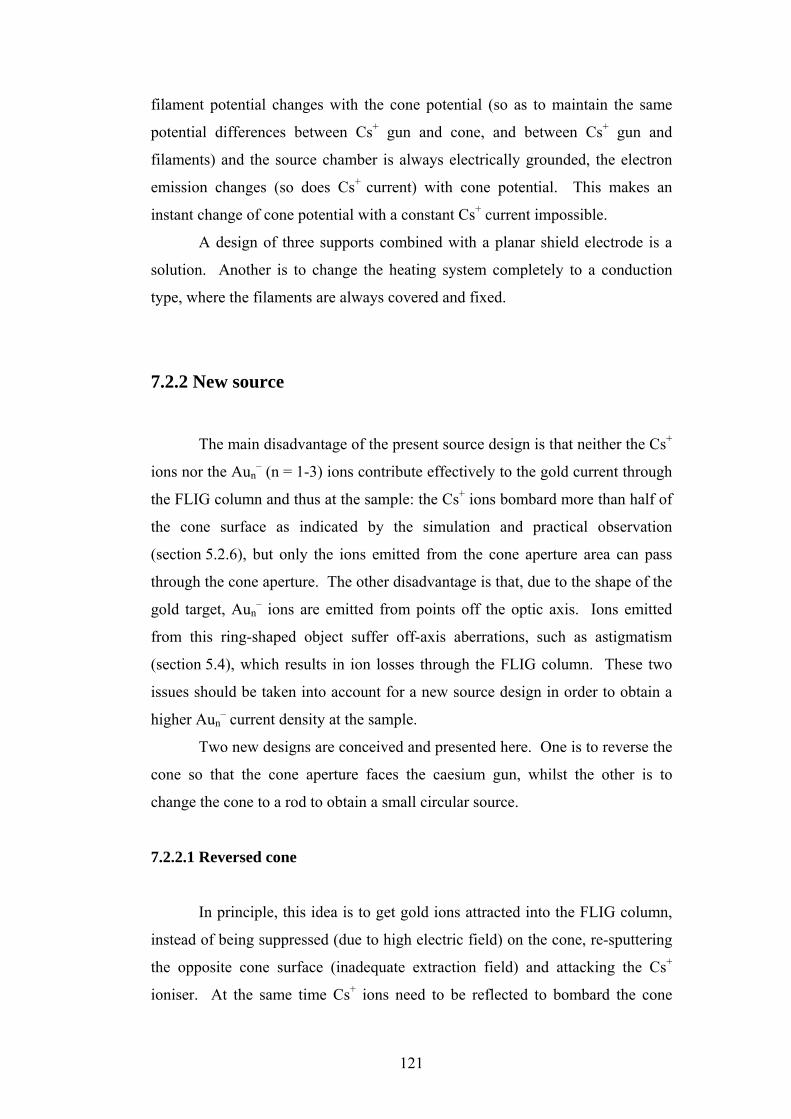
filament potential changes with the cone potential (so as to maintain the same
potential differences between Cs+ gun and cone, and between Cs+ gun and
filaments) and the source chamber is always electrically grounded, the electron
emission changes (so does Cs+ current) with cone potential. This makes an
instant change of cone potential with a constant Cs+ current impossible.
A design of three supports combined with a planar shield electrode is a
solution. Another is to change the heating system completely to a conduction
type, where the filaments are always covered and fixed.
7.2.2 New source
The main disadvantage of the present source design is that neither the Cs+
ions nor the Aun– (n = 1-3) ions contribute effectively to the gold current through
the FLIG column and thus at the sample: the Cs+ ions bombard more than half of
the cone surface as indicated by the simulation and practical observation
(section 5.2.6), but only the ions emitted from the cone aperture area can pass
through the cone aperture. The other disadvantage is that, due to the shape of the
gold target, Aun– ions are emitted from points off the optic axis. Ions emitted
from this ring-shaped object suffer off-axis aberrations, such as astigmatism
(section 5.4), which results in ion losses through the FLIG column. These two
issues should be taken into account for a new source design in order to obtain a
higher Aun– current density at the sample.
Two new designs are conceived and presented here. One is to reverse the
cone so that the cone aperture faces the caesium gun, whilst the other is to
change the cone to a rod to obtain a small circular source.
7.2.2.1 Reversed cone
In principle, this idea is to get gold ions attracted into the FLIG column,
instead of being suppressed (due to high electric field) on the cone, re-sputtering
the opposite cone surface (inadequate extraction field) and attacking the Cs+
ioniser. At the same time Cs+ ions need to be reflected to bombard the cone
121

surface with minimum loss, as well as an extraction system to get Aun– ions
behaving such as emerging from a single object on the axis having least
aberration.
A preliminary design of reversed cone emission system was simulated,
and ion trajectories were shown in Fig. 7.2.3. The Cs+ ion trajectories are
displayed in Fig. 7.2.4. The definitions of Aun– and Cs+ ions are identical to that
in section 4.2.1.
As the surface where Aun– ions are emitted faces the extraction field, most ions
can escape into the FLIG column, instead of being suppressed by the “shield” or
attracted to the caesium gun as is in the present design. Nevertheless, since ions
still emit from off-axis points (0.5-2.5 mm apart from the axis) and not from the
same point on the optic axis, a large cross-over is formed at the variable aperture,
and astigmatism was observed. Shown in Fig. 7.2.3 (a), the ions emitted from
the 1st point (as defined in Chapter 4) form a cross-over of Ø 4 mm at the
variable aperture. With identical parameters of electrical potentials, (c) shows
that ions emitted from a point 1.5 mm apart from the 1st point form a cross-over
at 167 mm upper-stream from the variable aperture, and the beam waist of this
emission at the variable aperture is Ø 10 mm. The astigmatism due to off-axis
emission can be observed by comparing Fig. 7.2.3 (a) and (b), which show the
ion trajectories in two planes orthogonal to each other (i.e. and
planes): the object is imaged at a distance of 236 mm from the variable aperture
in the plane, but in the
yx ˆˆ − zx ˆˆ −
yx ˆˆ − zx ˆˆ − plane the image is formed 13 mm closer to
the variable aperture. Overall, although ions are no more constrained by an
aperture, altogether they form a beam subject to off-axis aberrations.
For the Cs+ ion emission, Fig. 7.2.4 (a), (b) and (c) display that ions emitted from
different areas are deflected to bombard different places of the cone. The figures
also show that the Cs+ ions can bombard electrodes other than the gold cone.
122

Cs+ ion gun condensing lens
revered cone variable aperture image
y
Fig. 7.2.3 The design of a reversed-cone emission system, and the simulation of Au1
– ion trajectories. (a) and (b) show the trajectories of ion emitted from the exit point in yx ˆˆ − and zx ˆˆ − plane respectively: images are formed at different places in different planes. (c) shows the trajectories of ions emitted from the point 1.5 mm apart from the exit point: a cross-over is formed at upper-stream of the variable aperture.
-axis(a)image
x -axis
(b)13 mm
(c)
167 mm

gold ion extractors
Cs+ ion extractor
Cs+ ion gun
reversed cone
Fig. 7.2.4 The simulation of Cs+ ion trajectories: ions emitted from different areas are deflected to bombard different places of the cone, they can also bombard electrodes other than the gold cone.
Conclusively, this reversed-cone design still suffers the problems of
aberrations and large losses of both Cs+ and Aun– ions, unless the Cs+ ions can be
controlled to bombard a certain region on the cone or a better extraction can be
designed to get Aun– ions imaged at the same point.
124

7.2.2.2 Gold rod
There are several advantages of a gold rod design. (i) The object,
ion-optics-wise, is a small disc on axis, instead of a ring, which reduces off-axis
aberrations. (ii) The object can be made as small as the practical limit in
focussing the caesium beam. (iii) Gold and caesium ions will not be wasted as is
in the cone design. (iv) The gold rod can be designed to be movable, so that the
sputtered tip will be replaced by shifting the rod; the source will not need to be
dismantled as frequently.
A preliminary design of emission system for the rod source is presented
in Fig. 7.2.5. This simulates 1 keV Au1– emission, and the Cs+ ions bombard the
rod tip with an energy of 6 keV. The lens 1 used for the duoplasmatron on
EVA 2000 and Atomika 4500 is employed (Fig. 3.2.1). Eighty one caesium rays
emitted from an area of Ø 500 μm with an initial angle of 90 o to the surface and
an initial energy of 0.1 eV, are focussed to a spot of Ø 300 μm or less at the gold
rod. The gold (Au1–) ions are emitted with an initial angle of 90 o and energy of
1 eV, they emit from an area of Ø 500 μm and can be focussed to the variable
aperture where the beam waist is about Ø 40 μm (note: here the distance between
the rod and the variable aperture is kept the same). After the variable aperture,
the Au1– beam is focussed at the sample with a spot size of about Ø 20 μm.
However, if space charge effects are taken into consideration, the designed
caesium emission system, with the provided potential parameters, can only emit
0.1 μA. If more current were to be emitted, some ions would stop at the extractor
aperture. Again, SIMION cannot simulate space charge properly, and the
simulation done here is only provided as a qualitative reference. Fig. 7.2.5(b1)
and (b2) show the cases without and with space charge effects respectively. On
the other hand, space charge effects should not affect the Au1– beam as severely,
because the current is much smaller (10-4 of the Cs+ current), provided secondary
electrons can be removed. Assuming a maximum Au1– current of 50 nA is
achieved and the space charge effects are taken into account, the beam will be
focussed at the variable aperture and sample with a size of about Ø 200 μm and
Ø 70 μm respectively.
125
(a) (b1) (b2) + 5 kV
0 kV
+ 4.75 kV
– 1 kV
gold rod
+ 0.845 kV + 6.5 kV + 5 kV + 1.66 kV + 3 kV
FLIG column retarding lens
0 kV
Cs+ ion gun
(b1) &(b2)
(a) + 0.05 kV
Fig. 7.2.5 The design of a gold-rod SCIS. The green rays denote the Cs+ ions, and the blue the Aun– ions. Inset (a) shows the Aun
– ion emission system, (b1) shows the emission of a Cs+ current of 0.1 μA, and (b2) of 0.2 μA where space charge effects make some ions stop at the extractor aperture. (SIMION cannot simulate space charge properly; there is no way of relating the current to any “real” current.)

Overall, the main issue that needs to be considered for such a design is the space
charge effects that may occur for the caesium ion beam, which influences the
caesium current density falling on the gold rod. The caesium ions which do not
fall on the rod tip will not only be a loss, but also lead to the problems of caesium
coverage on insulators and undesirable sputtering.
127

Reference
Alton G D, Rev. Sci. Instum. 59(7) (1988) 1039.
Andersen H H and Bay H L, J. Appl. Phys. 45 (1974) 953.
Andersen H H and Bay H L, J. Appl. Phys. 46 (1975) 2416.
Appelhans A D and Delmore J E, Anal. Chem. 61 (1989) 1087.
Barlow R D, Dowsett M G, Fox H S, Kubiak R A A and Newstead S M, Nucl.
Instr. and Meth. in Phys. Res. B72 (1992) 442.
Billen James H, IEEE Transactions on Nuclear Science, NS-28 (1981) No. 2.
Belykh S F, Evtukhov R N, Lysenko Ju N and Rasulev U Kh, Rev. Sci. Instrum.
63(4) (1992) 2458.
Belykh S F, Development of a negative cluster ion source for mass spectrometry
of secondary ions and secondary neutrals. NATO SfP Project No. 97.1929
(1997)
Belykh S F, Bitensky I S, Mullajanov D and Rasulev U Kh, Nucl. Instr. and
Meth. in Phys. Res. B129 (1997) 451.
Belykh S F, Rasulev U Kh, Samartsev A V and Veryovkin I V, Nucl. Instr. and
Meth. in Phys. Res. B136 (1998) 773.
Belykh S F, Habets B, Rasulev U Kh, Samartsev A V, Stroev L V and
Veryovkin I V, Nucl. Instr. And Meth. in Phys. Res. B164-165 (2000a)
809.
Belykh S F, Rasulev U Kh, Samartsev A V, Stroev L V and Zinoviev A V,
Vacuum 56 (2000b) 257.
Belykh S F , Kovarsky A P , Palitsin V V, Adriaens A, Adams F, Int. J. Mass
Spectrom. 209 (2001) 141.
Belykh S F, Kovarsky A P, Palitsin V V, Adriaens A, Adams F, Appl. Surf. Sci.
203-204 (2003a) 122.
Belykh S F, Kovarsky A P, Palitsin V V, Adriaens A, Adams F, Nucl. Instr. And
Meth. in Phys. Res. B203 (2003b) 164.
Belykh S F, private communication, 2004.
Belykh S F, private communication, 2006.
Belykh S F, private communication 2007
Benninghoven A, Chemical Physics Letters 6 (1970) 626.
128

Benninghoven A, Int. J. Mass Spectrom. Ion Phys. 53 (1983) 85.
Bishop H E, Moon D P, Marriott P and Chalker P R, Vacuum 39 (1989) 929.
Blain M G, Della-Negra S, Joret H, Le Beyec Y, Schweikert E A, Phy. Rev. Lett.
63 (1989) 1625.
Cataing R and Slodzian G, J. Phys. E14 (1981) 1119.
Chait B T and Standing K G, Int. J. Mass Spectrom. Ion Phys. 40 (1981) 185.
Chambost E de, Boyer B, Rasser B and Schuhmacher M, Secondary Ion Mass
Spectrometry XII (2000) 533, Elsevier, Amsterdam.
Chang R J H, Belikh S F and Dowsett M G, unpublished design, 2005.
Cheng Juan and Winograd Nicholas, Anal. Chem. 77 (2005) 3651.
Clegg J B, Surf. Inter. Anal. 14 (1989) 307.
Chu D P and Dowsett M G, Phys. Rev. B56 (1997) 15167.
Cooke G A, Ph.D. thesis (1992) University of Warwick.
Dahl D A, SIMION 3D Version 7.0 User’s Manual (2000), BECHTEL BWXT
IDAHO, LLC.
Davies N, Weibel D E, Blenkinsopp P, Lockyer N, Hill R, Vickerman J C, Appl.
Surf. Sci. 203-204 (2003) 223.
Döbeli M., Nebiker P W, Mühle R, Suter M, . Instr. And Meth. in Phys. Res.
B132 (1997) 571.
Dowsett M G, unpublished, 1986.
Dowsett M G, McPhail D S, Parker E H C and Fox H, Vacuum 36 (1986) 913.
Dowsett M G and Clark E A, Practical Surface Analysis Ch. 5, Vol. 2, 2nd Ed.,
Wiley (1992).
Dowsett M G, Thompson S P and Corlett C A, Secondary Ion Mass
Spectrometry VIII (1992) 187, Wiley.
Dowsett M G, Smith N S, Bridgeland R, Richards D, Lovejoy A C and Pedrick P,
Secondary Ion Mass Spectrometry X (1997) 367, Wiley.
Dowsett M G, Appl. Surf. Sci. 203-204 (2003) 5.
Dowsett M G, private communication, 2007.
Dowson P H, in Quadrupole Mass Spectrometry and Its Applications, Elsevier,
Amsterdam (1976).
El-Kareh A B and El-Kareh J C J, Electron Beams, Lenses, and Optics (1970),
Academic Press.
Finkelstein A F, Rev. Sci. Instrum. 11 (1940) 94.
129

Gassiot J P, Philos. Trans. Roy. Soc. London 148 (1858) 1.
Gerlach R, Secondary Ion Mass Spectrometry, SIMS III, Springer Series in
Chemical Physics Vol. 19, p. 22, Springer, Berlin (1982).
Gillen Greg, King R. Lance and Chmara Frank, J. Vac. Sci. Technol. A17(3)
(1999) 845.
Gillen Greg, King Lance, Freibaum Brian, Lareau Richard, Bennett Joe and
Chmara Frank, J. Vac. Sci. Technol. A 19(2) (2001) 568.
Gillen Greg, Batteas James, Michaels Chris A, Chi Peter, Small John, Windsor
Eric, Fahey Albert, Verkouteren Jennifer, Kim K J, Appl. Surf. Sci. 252
(2006) 6521.
Gillen Greg, 44th IUVSTA Workshop: Sputtering and Ion Emission by Cluster Ion
Beams, Scotland UK, 2007.
Goldstein E, Verh. Dtsch. Phys. Ges. 4 (1902) 228.
Goodhew Peter J, Humphreys John and Beanland Richard, Electron Microscopy
and Analysis Ch. 6, 3rd Ed. (2001), Taylor & Francis Inc.
Grove W R, Phil. Mag. 5 (1853) 203.
Herzog R F K and Vieböck F, Phys. Rev. 76 (1949) 855.
Hofer W O, Liebl H, Roos G and Straudemaier G, Int. J. Mass Spectrom. Ion
Phys. 19 (1976) 327.
Iltgen K, Bendel C, Benninghoven A and Niehuis E, J. Vac. Sci. Technol. A15(3)
(1997) 460.
Jede R, Ganschow O, Kaiser U, Practical Surface Analysis Ch. 2, Vol. 2, 2nd Ed.,
Wiley (1992).
Jiang Zhi-Xiong, Alkemade Paul F A, Algra Eelke and Radelaar S, Surf.
Interface Anal. 25 (1997) 285.
Kilner J A, Beyer G P and Chater R J, Nucl. Instr. and Meth. in Phys. Res. B84
(1994) 176.
Klemperer O, Electron Optics, 3rd Ed., Cambridge University Press (1971).
Kollmer F, Appl. Surf. Sci. 231–232 (2004) 153.
Krohn V, J. Appl. Phys. 33 (1962) 3523.
Lide David R (Edtor-in-Chief), CRC Handbook of Chemistry and Physics
2007-2008, TF-CRC (2007)
Liebl H, Nucl. Instrum. Meth. 187 (1981) 143.
130

Liu J R, Wang X M, Shao L, Chen H and Chu W K, Nucl. Instr. and Meth. in
Phys. Res. B197 (2002) 101.
Littlewood S D and Kilner J A, J. Appl. Phys. 63 (1988) 2173.
Littmark U and Hofer W O, Nucl. Instr. and Meth. 168 (1980) 329.
Longhurst R S, Geometrical and Physical Optics, Ch. 2, 2nd Ed. (1967) Longman.
Mahoney C M., Roberson S V and Gillen Greg, Anal. Chem. 76 (2004) 3199.
Maier M, Vacuum 36 (1986) 409.
Massey H S W and Burhop E H S, Electronic and Ionic Impact Phenomena
Ch IX (1952), Oxford University Press.
Maul J L and Wittmaack K, Surf. Sci. 47 (1975) 358.
Medvedeva M, Wojchiechowski I, Garrison B J, Appl. Surf. Sci. 203-204 (2003)
148.
Middleton R and Adams C T, Nucl. Instrum. and Meth. 118 (1974) 329.
Middleton R, Nucl. Instrum. and Meth. 144 (1977) 373.
Miwa Shiro, Nomachi Ichiro, Kitajima Hideo, Appl. Surf. Sci. 252 (2006) 7318.
Mohoney J F, Perel J and Forrester A T, Appl. Phys. Lett. 38 (1981) 320.
Morris R J H, private communication 2007.
Nagamachi Shinji, Yamakage Yasuhiro, Maruno Hiromasa, Ueda Masahiro,
Sugimoto Seiji, Asari Masatoshi and Ishikawa Junzo,
Appl. Phys. Lett. 62 (1993) 2143.
Newton G and Unsworth P J , J. Appl. Phys. 47 (1976) 70.
Nielsen K O, Nucl. Instrum. 1 (1957) 289.
Nier A, Rev. Sci. Instrum. 18 (1947) 398.
Paul W and Steinwedel H, Zeitschrift Für Naturforschung 8a (1953) 448.
Paul W, Reinhard H P and Zahn U von, Z. Phys. 152 (1958) 143.
Reuter W and Wittmaack K, Applications of Surface Science 5 (1980) 221.
Prewett P D, Jefferies D K and McMillan D J, Vacuum 34 (1984) 107.
Ronsheim P A, Appl. Surf. Sci. 252 (2006) 7201.
Rybalko V F, Kolot V Ya and Fogel Ya M, Soviet Phys.-Solid State 11 (1959)
1142.
Samartsev A V, Duvenbeck A and Wucher A, Phys. Rev. B72 (2005) 115417.
Samartsev A V and Wucher A, Appl. Surf. Sci. 252 (2006) 6474.
Sigmund P, Phys. Rev. 184 (1969) 383.
Sigmund P, Appl. Phys. Lett. 25 (1974) 169.
131

Sigmund P, Sputtering processes: Collision Cascades and Spikes, Inelastic
on-Surface Collisions, Ed. by Tolk N H, Tully J C, Heiland W and
White C W, Academic Press Inc., New York (1977) 121.
Sigmund P, Sputtering by particle bombardment. I. Physical sputtering of single
element solids. Ch. 2, Topics in Applied Physics, Ed. by R. Behrisch, 47
(1981) Springer.
Sigmund P and Claussen C, J. Appl. Phys. 52(2) (1981) 990.
Slodzian G, Applied Charge Particle Optics B, Advances in Electronics and
Electron Physics, Ed. Septier A, Vol. 13, p. 1, Academic Press, New York
(1980).
Slodzian G, Girard F, Boust F and Hillion F, Proceedings of Secondary Ion Mass
Spectrometry Conference VIII, Ed. by Benninghoven A, Janssen K T F,
Tumpner J, and Werner H W, Wiley (1992).
Smith N S, Ph.D. thesis (1996) University of Warwick.
Stevie F A, Kahora P M, Simons D S and Chi P, J. Vac. Sci. Technolol. A6 (1988)
76.
Sykes D E, Chew A, Surf. Interf. Anal. 21 (1994) 231.
Szymczak W, Wittmaack K, Nucl. Instrum. Meth. B88 (1994) 149.
T rvi T T, J. Pakarinen A, Kuronen A and Nordlund K, EPL 82 (2008) 26002. a&&
Thompson D A and Johar S S, Appl. Phys. Lett. 34(5) (1979) 342.
Thompson D A, Radiat. Eff. 56 (1981) 105.
Thomson J J, Philosophical Magazine 20 (1910) 752.
Urbassek H M and Michl J, Nucl. Instr. and Meth. in Phys. Res. B22 (1987) 480.
Vályi L, Atom and Ion Sources (1977), John Wiley & Sons.
Vancauwenberghe O, Hellman O C, Herbots H, Tan W J and Olson J, Mater. Sci.
Eng. B12 (1992) 97.
van der Heide P A W, Lim M S, Perry S S and Bennett J, Nucl. Instr. and Meth.
in Phys. Res. B201 (2003) 413.
Veryovkin I V, Belykh S F, Adriaens A, Adams F, Instr. And Meth. in Phys. Res.
B219-220 (2004) 215.
Vandervorst W, Appl. Surf. Sci. doi: 10.1016/j.apsusc.2008.05.090.
Wagner M S, Surf. Interface Anal. 36 (2005) 42.
Wagner M S, Surf. Interface Anal. 36 (2005) 53.
Wagner M S, Surf. Interface Anal. 36 (2005) 62.
132
Wien W, Annal. Phys. 8 (1902) 260.
Williams P, Surf. Sci. 90 (1979) 588.
Wittmaack K, Appl. Phys. Lett. 29 (1976) 552.
Wittmaack K, Surf. Sci. 90 (1979) 557.
Wittmaack K, Nucl. Instr. Methods. 168 (1980) 343.
Wittmaack K, Wach W, Nucl. Instr. and Meth. 191 (1981)327.
Wittmaack K, Vacuum 32 (1982) 65.
Wittmaack K and Poker D B, Nucl. Instr. and Meth. in Phys. Res. B47 (1990)
224.
Wittmaack K, Practical Surface Analysis Ch. 3, Vol. 2, 2nd Ed., Wiley (1992).
Wittmaack K, Nucl. Instr. and Meth. in Phys. Res. B85 (1994) 374.
Wong S C C, Hill R, Blenkinsopp P, Lockyer N P, Weibel D E and
Vickerman J C, Appl. Surf. Sci. 203-204 (2003) 219.
Yamada Isao, Matsuo Jiro, Toyoda Noriaki, Kirkparick Allen, Materials Science
and Engineering R34 (2001) 231.
Zalm P C and Vriezema C J, Nucl. Instr. and Meth. in Phys. Res. B64 (1992) 626.
Zimmermann Steffen, Urbassek Herbert M, Int. J. Mass Spectrom. 272 (2008)
91.
133