a time-division analogue multiplier for correlation...
TRANSCRIPT

MINISTRY OF AVIATION
AERONAUTICAL RESEAR6-l COUNCIL
CURREN J PAPERS
A Time-Division Analogue Multiplier for
Correlation Measurements and Mixing at
Frequencie,s up to 100 Kilocycles per Second
BY
RI. Johnson, B.A., BSc.,
LONDON: HER MAJESTY’S STATIONERY OFFICE
1963
SIX SHILLINGS NET

C.P. No.605
2.
3.
4.
5.
6.
7.
a.
A Time-Division Analogue Multiplier for Currelation Measurements and Mixing at Frequencies up to
100 Kilocycles per Second -By-
R. F. Johnson, B.A., B.Sc.
AumTust, 1962
List of Contents
SUMMARY . . . . . . . . . . . . .
Introduction . . . . . . . . . .
Multiplication Methods . . ;. . . 3.1 Quarter squares . . . . . . 3.2 Logarithmic . . . . . . . . 3.3 Hall effect ., . . . . . . 3.4 Time division . . . . . .
General Description of the Mdtiplxer It.1 The use of feedback . . . .
Circuit Details . . . . . . . . 5.1 The X input amplifier . . . . 5.2 The moaulator . . . . . . 5.3 The switch empliflers . . . . 5.4 The transistor switches ,.. 5.5 The phase inverting amplifier 5.6 The cutput amplifier . . . . .
l%e Complete Instrument . . . . 6.1 Circuit details . . . . . . 6.2 Operation . . . . . . . .
Performance of Multiplier . . . . 7.1 Limitations on accuracy . . 7.2 Performance f?-lmmq . . . .
Applications of the Multiplier . .
. .
. .
. . . . . . . . . .
. . . .
. .
. .
. .
. .
. . . . . .
. .
. . . .
. .
. .
. .
. .
. . .
. .
,. . . *. . . . .
. .
. .
. .
. .
. .
. .
. .
. .
. .
. .
. .
. .
,. . . . .
. .
. .
. .
. .
. . . . . . . .
. .
. .
. .
. . . . . . . . . . . .
. . . . . .
. .
. .
. .
. .
. .
. .
. .
. .
. . . . . .
. . . .
. .
. . . . . . . . . . . .
. .
. .
. .
. .
. .
. .
. .
2
2
4 5
: 8
8 9 9
10
9./ -_----_----__r---_-_-- p--v- _____-_-----r--------
Replaces N.P.L. Aero ReportNo.~O30 - A.R.O.23,pn. Published with the permission of the Director, National Physical Laboratory.

-2-
9. conclusions . . . . . . . . . . . .
IO. Aclaxxvledgement . . . . . . . . . .
References . . . . . . . . . . . .
Appendix I -Setting-up Procedure . .
Appendix II - Constructional Details . .
. .
. .
.,
. .
. .
. . . .
. . . .
. . . .
. . ,.
. . . .
w
IO
10
Ii
43
15
For processing noise and turbulence signals there is a need for an analogue multiplIer capable of handlzng input frequencies from a few cycles to about SO kilocycles per second. Previous circuits descrxbed have been unduly complex or restricted in frequency response. A circuit for a time-division multiplier 1s described capable of accepting signals from zero frequency to 100 kc/s. Preamplifiers and associated circuits are described which enable the multiplrer to be used for the measurement of a wide range of parameters encountered in the turbulence and noise field.
2. Introduction
Fluctuations of velocity or pressure in or near a turbulent flow may be converted into fluctuating electrical signals by the use of suitable transducers. For example, a hot v&-e anemometer may be used to produ e an electrical signal proportional to the fluctuatmg velocity in a jet', . whxh will contain energy up to approximately 100 kc/s if the exit diameter is one inch and the mean velocity a few hundred feet per second.
In order to obtain information from these signals they must be passed through processing equipment, to yield such functions as the mean square and higher powers, the autocorrelationvxefficient and the coefficient of correlation between two sipls. In generating most of the functions of aemdynsmic significance it is thus necessary to operate upon the signals at some stage with a multiplier. square value, VW,
For example the mean of a signal v(t) is the mean or zero frequency
output of.the multiplier when the signal is fed into both inputs. This function, or the root mean square value, can obviously be derived by the use of a true R.&S. meter such as a thermocouple instrument, but the
measurement/
-3-
measurement of correlation coefficients and mean values of higher powers requires the derivation of instantaneous squares or products, thus making a multiplier essential.
3. Multxplicatlon Meth&
Since most multipliers are designed for use in analogue computers, the accuracy is good (usually better than 0.1% of full output) but the frequency response is restricted to under I kc/s. A number of methods to effect the multiplication of two signals has been devised, and a few of these methods, excluding mechanical techniques, will be brIefly mentioned.
3.1 Quarter squares
The principle of quarter squares, using the identity
r?J = i[ (x+y)” - (x-Y)‘1
reduces the problem of multiplication to one of generating the square of a function.
,$gp
This may be carried out by the use of a no$-$l"ear element or such as a chain of silicon carbde resistors 9 or of blased
however both these methods are limited z.n frequency response, the former to about 400 c/8 and the latter to about 20 kc/s. An accurate squarxng device with a very good frequency response can be made using the deflection of an electron beam past an effectively parabolic-shaped mask4~5, the resulting anode current being proportional to the square of the deflecting plate potential. The accuracy of the multlpller descrxbed 1~1 Ref. 4 is about 0.5$ of the maxjmum output and the frequency response is restricted mainly by the necessary drivmg amplifiers, that of the squaring tubes themselves berg many MC/S. A disadvantage of this system is the high cost of the tubes and the care needed with the physical layout of high impedance clrcultry at the higher frequencies.
3.2 Logarithmic
It is also possible to mullapply two functions using the relation
log g = log x + logy,
and to recover the product by taking the antilogarithm of the sum. However, the generation of the logarithmic f'unction, usually performed by diodes, is limited in frequency response to under 1 kc/s (Ref. 6). Some sermconductor &odes exhxbit a logarithmic -en&voltage characteristic over a wide range of applwd voltage and it may thus be possible to reduce the number of elements required for a given accuracy and hence increase the frequency response.
3.3 Hall effect
The Hall effect7, whereby in .some materials a potential is developed which 1s proportional to the product of the transverse current
flowing/

-4-
flowing and the magnetic field 111 which the material is placed, can be used to generate the pmduct of two signals. This device is capable of working up to high frequencies, the main diffxulty being to provide the ma@etic field without phase shift ana stray coupling to the output circuit. By careful design of the cods and by the us of correction fields the Hall effect has been used at radio frequencies 8 9 10 y 5 . However, commercdly available models do not appear to have frequency responses in excess of 10 kc/s; accuracies at these frequencies are about O.$ of maxirmM output.
3.4 Time division
used"-'8 The principle of time division in multlplicatlon has been widely
. An input signal x(t) IS sampled em3 causes signal y(t) to be switched on for a txne pmportional to the instantaneous value of X. If the rate of sampling is much hxgher than the highest frequency component m x(t) or y(t), the output may be passed through a low-pass filter to remove the carrier frequency giving a filtered output proportional to both x(t) and y(t) and hence to the product w. In the crrcuits described IIL Refs. 11 to 15 the highest samplrng rate is a few kilocycles per second and hence the maxmum frequency of input is restrxted to an order less thsn thus, or about 1 kc/s. The accuracy xn these circuits is better than O.$ of full output.
4. General Descrxptxon of the Multiplier
' In view of the lack of frequency response of etisting designs, a new multiplier has heen developed for the N.P.L. noise and turbulence research progrsnnns. A time divlsion multlplxer, (U.K. Pat. App. 8203/61; D.S.I.R. Pat. 24/1540/l) workmg up to 20 kc/s has been described by Barber'% the baalc circuit to be described is a development from this.
A block diagram showing the principles of the multiplier is given in Fig. 1. The X signal contmls the Mark/Space Mcdulator dich generates a train of rectangular pulses. The departure from unity mark/space ratlo of these pulses 1s pmportional to the instantaneous value of the input signal X, so that ti u is the fraction of time that the output of the Modulator is in the "switch on" state, we have:-
1 +Ax a =
2 * . ..(I)
The Modulator also generates sn antiphase sRntching signal such that
1 -AX a* = -
2 . ..(2)
where A is the modulation constant.
These trains of pulses are used to operate switches to gate the Y signal. When the sixLtchi.ng signal is in the "switch on" state, rmritch SI
is/

-5-
is open and the potential at A rises to +Y. When the switching signal is in the "off"' state & is closed and the potential at A falls to aero. Thus the sxgcsl at A is a train of pulses having the same width and repetition rate as the Modulator pulse train, but with pulse height +Y. Similarly the signal at B is the inverted pulse train having height -Y. The signal at A now passes through a Phase Inverting Amplifier and Is added to the B signsl. The resultant at C is a rectangular wave signal between +Y/2 and -Y/2. The fractxon of time spent in the +Y/2 state
1 +Ax 1 -Ax iS , and in the -Y/Z state,
2 * If the mean value of thlS
2 signal is obtained by passing it through a filter that removes the carrier signal but passes the signal frequency wthout appreciable phase-shift, the output v, 1s given by:-
v, = (;).('+J+(-;).(';">
AXY =-=Kxy.
2
Thus the output 1s proportional to the product of X and Y.
. ..(3)
4.1 The use of feedback
The basic principle of Fig. 1 is used as shown in Fig. 2. The Mark/Space Modulator, 2, is controlled by the X Input Ampltiier, 1. The two trains of switching pulses are passed through a pair of Switch Amplifiers, 3. The output of one of these Switch Amplifiers is used to apply negative feedback to the Modulator; the pulse train at this point has a constant peak-to-peak amplitude with mark/space ratio given by
I -AX af = .
2
If the mean potential of this pulse train for unity mark/space ratio is zero, and the pulse height is 2X', then the mean value, Vf is given by
v. = 1 K'AX. . ..(4)
Hence it is possible to apply negative feedback in the usual way from the output of the Switch Amplifier stage to the X Input Amplifier, and thus linearise the departure from unxty mark/space ratio with the applied input signal X.
The Switches, 4, and Phase Inverting Amplifier, 5, are used as described in Section I+ above. An Output Amplifxer, 6, is used to give a low Output impedance and isolate the summing junction, C from load effects.
This/

-6-
This amplifxr also acts a8 a low pass filter by the inclusion of a capacitor, C' m Its feedback path.
5. Circuit Details
5.1 The X Input Amplifier (Fig. 3) is a long-tailed pair of silicon transistors, B-3 and Tr4, mounted on a common heat sink to minimise effects of temperature difference and hence reduce drift. The base of Tr3 is taken to an adJustable potentxil to allow the currents flowing in the collectors of these input transistors to be set differentially as described below. For convenience 'coarse1 and 'fine' balance controls are provxled, the latter being on the front panel of the instrument. The X mput is applied to the base of Tr4 via an 8.2K resistor, giving an input sensitivity of about +4V for maximum output; the value of this reslstor may be changed to give different input sensltivztle.9.
5.2 The Modulator, conslstme, of !Tr5 and TX-6, is a symmetrical, emitter-coupled multivibrator circuit. The deviation from unity mark/space ratio is proportional to the ratio of the currents in these two transistors. This ratio is controlled by the currents in 'JY3 and Tr4 and hence by their base potentials. For equal currents the repetition frequency is approximately xc/s; at the maximum excursion of the X input signal this repetition rate falls to about 800 Kc/s when the mat-k/space ratio is about 1O:l. Thus at themaxirmun excwsxons of the X ylputslgnalthe sampling rate decreases; the high-frequency response of the multIplier is thereby reduced. The balance controls VRI and VR2 are used to set the mark/space ratio to unity when X = 0. A variable collector loaa, VR4 IS used to equalise the outputs of Tr5 and ~r6, to overcome varxations in component values.
5.3 The Swatch Amplifiers Tr2 and l'r7 are directly coupled to the collectors of Tr5 and Tr6. Negative feedback is taken from a tapplns in the collector load of Tr7 at such a point that the mean potential-for- unity mark/space rat10 is zero. The negative feedback is applied by returning the 470 ohm reslstor in the base circuit of Tr4 to the output of the feedback filter, 2.7KC and IO&F. Tne amplitude of the pulse trains at the collectors of !lW and Tr7 is approximately +4 volts.
5.4 The Transistor Switches Trl and Tr8 operate in the growded emitter configuratxon and are driven from the collectors of Tr2 and Tr7 via the diodes Di and D2. These act as catchers which prevent the reverse base-edtter voltage exceeding the limit of 3 volts for the 2N706. (Types 2~706A and 2N706B may be used here and elsewhere in the circuit with mme advantage. Both have a higher reverse emitter-base voltage limit of 5V, and the latter type a lower emitter-collector saturation voltage.) When the base potential of the mtching transistor is positive the impedance between emitter and collector falls, and the transistor "turns on" thus switching off the signal at the collector. The mean potential of the collectors can be set by VR5 to mi.nznx.e the component of X signal in the output when Y = 0. vR3 compensates for dirferences in the transistor switches and is set for minimum output when Y is at madmum a.c. signal and x = 0. The outputs from the collectors of Trl and PI-~ are fed respectively to the Phase Inverter and Output Amplifier, Fig. 4.
5.5/
-7-
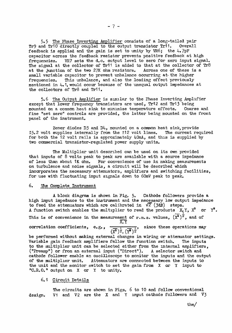
5.5 The phase Inverting Amplifier consists of a long-tailed pair fry and ~1-10 directly coupled to the output transistor Trll. Overall feedback is applied -&d the gain is set to unity by VR~; the 4.7pF capacitor across the feedback resistor prevents positive feedback at high frequencies. VR7 sets the d.c. output level to zero for zero input signal, The signal at the collector of ~rll is added to that at the collector of Tr8 at the junction of the two 27X ohm resistors. Across one of these is a small variable capacitor to prevent unbalance occurring at-the higher frequencies. This unbalance, and also the loading effect previously mentioned in 4.1,would occur because of the unequal output impedances at the collectors of Tr8 and WI.
5.6 The Output Amplifier is slmllar to the Phase Inverting Amplifier except that lower frequenc.y transistors are used, Tri2 and l'r13 being mounded on a common h&at sink to nunlmise temperature effects. Coarse and. fine "set zero" controls are provided, the latter being mounted on the front panel of the instrument.
Zener diodes D3 and D4, mounted on a common heat sink,provide 55.2 volt supplies internally from the 212 volt lines. The current required for both the 12 volt rails is approximately 4CmA, and thu is supplied by two cwercial transistor-regulated power supply units.
The Multiplier unit desorlbed can be used on its own provided that inputs of 8 volts peak to peak are avallable with a source impedance of less than about 1K ohm. For convenience of use in making measurements on turbulence and noise signals, a circuit will be described which incorporates the necessq attenuators, smpliflers and switching facilities, for use with fluctuating input szgnals down to 60mv peak to peak.
6. The Complete Instrument
A blook diagrsm is shown in Fig. 5. Cathode followers provide a high input impedance to the instrument and the necessary low output impedance to feed the attenuators which are calibrated in fi (JdB) steps. A function switch enables the multIplier to read the products XY, 2 or p.
-3. This is of convenience in the measurement of r.m.s. values, (x")", and of
x. correlation coefficients, e.g.,
(F)S. (F)$' since these operations may
be performed without making external changes in wiring or attenuator settings. Variable gain feedback amplifiers follow the function switch. The inputs to the multiplier unit can be selected either from the internal amplifiers, ("Presmp") or from an external input ("Direct"). A selector switch and cathode follower enable an oscilloscope to monitor the inputs and the output of the multiplier unit. Attenuators ars connected between the inputs to the unit and the monitor switch to set the gain from X or Y input to "C R 0 ' output on X or Y to unity. . * .
6.1 Circuit Details
The circuits are shown in Figs. 6 to IO and follow conventional design. VI and V2 are the X and Y Input cathode followers and V3
the/

-a-
the C.R.O. cathode follower. V&-V6 and V7-V9 are the preamplifiers with overall negative feedback applied vza the cathode circuit, of the first stages. The outputs of these ampllriers have two stages of hzgh pass RC filtering (IOOpF, 8.2Kn and IOOuF, 18Kn) to prevent any spurious d.c. reaching the input of the multiplier unit. Catcher diodes Dj-D6 are also included at this point to prevent any transients m excess of 12 volts causing damage to the transistors. For this purpose also, diodes D7 and D8 (Fig. 9) remove the hxgh voltage pulse generated when the relay is de-energised.
Details of the d?- attenuator are shown in Fig. 10. Most of the values are made up from two resistors in series, selected from $ matt high stability carbon resistors to an accuracy of 50.1%. The switch is an 11 wryr "make before break" wafer switch.
6.2 Operation
In operation it is necessary only to adjust VR9 for zero output with both input attenuators at "O", and to adjust VRI for minimum output for X = 0 and Y = maximum signal. The input level of the signals are set by observing the C.R.O. output and setting the attenuators to give less than ~&IV peak to peak when the monitor switch is at "X" or "Y". The maximum input to the instrument is 1.3 volts peak to peak when the input
tt , 11 attenuators are on --z 0
1642
The output of the multiplier may be used to drive a galvanometer or other meter with an impedance greater than IKR, when measuring the mean value of the output signal. For greater ac cmracy when dealing with low frequencies the output may be fed to an integrator as described in Ref. 1.
Detads of the initial adJustments to the instrument are given in the Setting-up Procedure in Appendix I.
Appendix II gives details of the components used in the instrument.
7. Performance of Multiplier
The variation of percentage output error with input voltage in one quadrant 1s shown xn Fig. II. The drtit. of the output for zero input, which amounted to 0.3% of the output at J volts input during the course of the observations, has been subtracted from these results.
Dynem~c tests for the complete mstrument and attenuators are shown in Figs. 12 and 13. The effect of slight overload 1s shuw-n when the attenuators are in the "1" setting.
Fig. 14 demonstrates the dynamic range of the instrument when used as a? operational squaring devxe, with 1 kc/s sinewave inputs. The outputs were within 0.1 dB of the correct value over a dynamic output range of 60 dB, the results at 80 kc/s input frequency being within 0.2 dB over the same range.
-9-
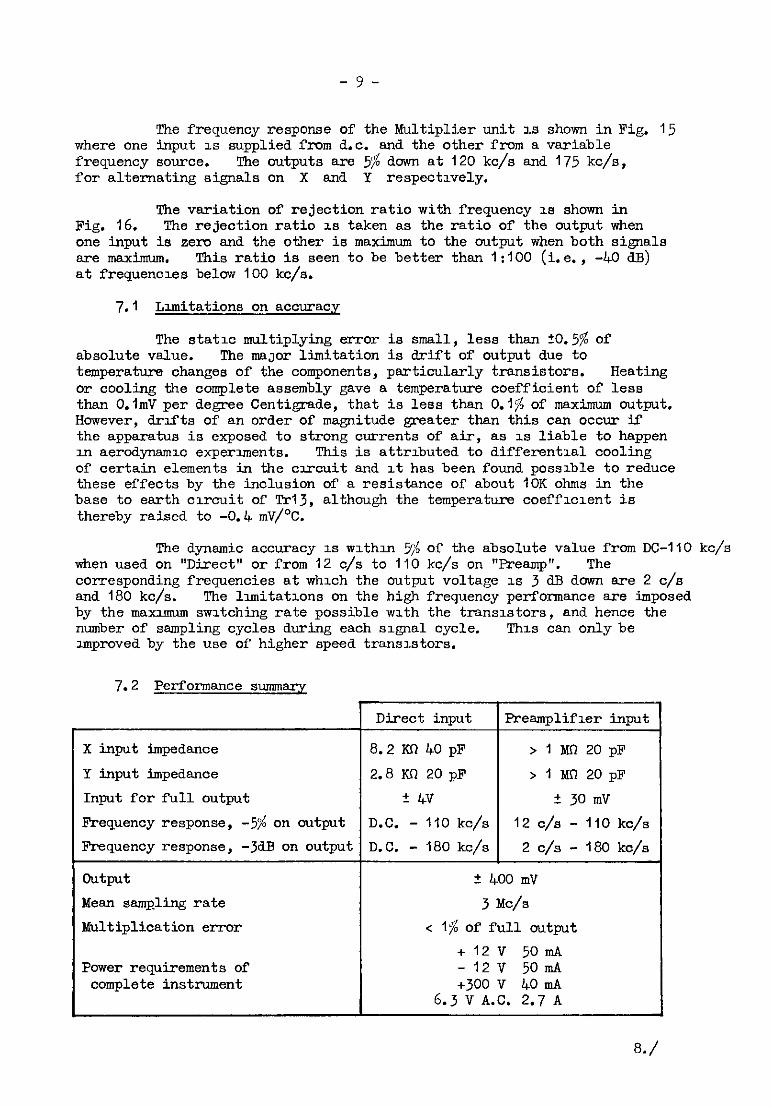
The frequency response of the Multiplier unit 1s shown in Fig. 15 where one input 1s supplied from d.c. and the other from a variable frequency source. The outputs are @ down at 120 kc/s and 175 kc/s, for alternating signals on X and Y respectively.
The variation of rejection ratio with frequency 1s shown in Fig. 16. The rejection ratio IS taken as the ratio of the output when one input is zeru and the other is maximum to the output when both signals are maxirmun. This ratio is seen to be better than I:100 (i.e., -40 dB) at frequencies below 100 kc/s.
7.1 Lzmitations on accuracy
The static multiplying error is small, less than +0.5$ of absolute value. The maJor limitation is drift of output due to temperature changes of the components, particularly transistors. Heating or cooling the complete assembly gave a temperature coefficient of less than O.ImV per degree Centigrade, that is less than 0.1s of maximum output. However, drifts of an order of ma@tude greater than this can ocour if the apparatus is exposed to strong currents of air, as 1s liable to happen m aerodynamic experiments. This is attributed to different181 cooling of certain elements in the crrcuit and It has been found posszble to reduce these effects by the inclusion of a resistance of about IOK ohms in the base to earth circuit of !l'rlj, although the temperature coefflolent is thereby raised to -0.4 mV/%.
The dynamic accuracy 1s wxthln 5$ of the absolute value from DC-110 kc/s when used on "Direct" or from 12 o/s to 110 kc/s on "Preanp". The corresponding frequencies at which the output voltage 1s 3 dB down are 2 o/s and 180 kc/s. The llmitatlons on the high frequency performance are imposed by the maxumun swltohing rate possible with the transistors, and hence the number of sampling cycles during each signal cycle. Thm can onlybe reproved by the use of higher speed transistors.
7.2 Performance swmnsry
X input impedance
Y input impedance Input for full output
Frequency response, -y$ on output Frequency response, -3dB on output
output
Mean sanqling rate Multiplication error
Power requirements of complete instrument
Direct input
8.2 Kil 40 pF
2.8 Kfl 20 pF + 4v
D.C. - 110 kc/s D.C. - 180 kc/s
1
I
?reamplifler input
> 1 MR 20 pF
> 1 MO 20 pF
+ 30 mv 12 o/s - 110 kc/s
2 c/s - 180 kc/s
?r 400 mv 3 MC/S
< I$ of full output +12v 5omA -12v 5omA +300 v 40 mA
6.3 V A.C. 2.7 A
8./
- 10 -
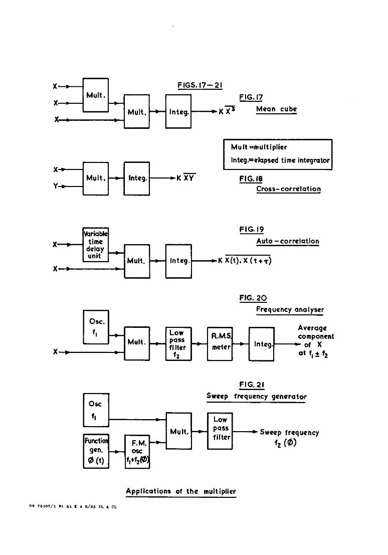
0. Applications of the Multiplier'
The application of the multiplier to the measurement of mean powers and of correlation coefficients has been mentioned 1~1 SectIon 2, and the block diagmms for such measurements are shown in Figs. 17, 18 and 19.
The multiplier may also be used as a mixer in a constant bandwidth frequency analyser as shown in Fig. 20. analysis is set by the sinewave oscillator at fi
The frequency of and the bandwidth, 2fa,
by the cutoff frequency of the low pass filter whxh passes signals having frequenczes from zero to fa.
A further use of the multiplier as a frequency changer 1s the generation of a sweep frequency, demonstrated. in the block diagram of Fig. 21. A function generator provides a voltage 6 varying with time. This potential controls the frequency of oscillation of the frequency modulation oscillator, whxh may be a square wave generator, giving a fundamental output frequency of fi + fs($). If thm output 1s multlplled by a signal with frequency fi in the multiplmr and the output passed through a low pass filter to pass fg but not fi or higher frequencies, the resultant ml1 be a frequency f,($). Thus if the function generator, (whxch may conveniently be a slow oscilloscope tune-base), provdes a saw-tooth waveform the resultant will be a frequency vsrylng linearly with time. The lowest frequencies obtainable xn this way are lunited solely by the rate of drift of the two oscillator frequencies, which may easdy be held to within a few cycles per second per minute when fi is about 100 kc/s. The upper frequency obtainable is limited by the low pass filter characteristics for a carrier frequency below 100 kc/s. Thus this system can provde a suitable sweep frequency for the response testing of apparatus encountered zn the turbulence and noise fxld of research.
The Integrator wed zn conJunction with the c&cults mentioned above is the elapsed time integrator described in Ref. 1, using an operational d.c. amplifier as the computing element and a dekatron ohaln 88 the tlm1ng clrcult.
9. Conclusions
The vanable mark/space Multiplier has proved very satisfactory for the measurement of a wide range of parameters in the turbulence and noise field, the accuracy and frequency response being amply adequate. The cost and smplicity are an addntage over any comparable multlplxr. The reliability has been excellent over an extended period of use.
IO. Acknowledgement
The author acknowledges the helpful discussions with D. L. A. Barber of the Autonomxs Divlslon, N.P.L.
References/
- 11 -
& Author(s) Title, etc.
1 Pp. Bradshaw and R. F. Johnson
An introduction to turbulence measurement with hot wz.re anemometers. parts I and II. NPL/Aem Notes/427 and 434. 1961. (To be publIshed in the N.P.L. Notes on Applied Science Series.)
2 L. D. Kovach and w. comley
3 Douglas Akcreft
4 J. A. Miller, A. S. Soltes and R. E. Scott
5 A. s. sdtes
6 Solsrtron
7 E. H. Hall
a R. P. Chasmar and E. Cohen
9 E. Cohen
IO E. Cohen
11 R. A. Meyers and H. B. Davis
References
A new, solid state, nonlinear analog component. I.R.E. Transactions on Electronic Computers, December 1960, pp.496-503.
co. The Douglas Quadratmn Type P. Douglas Aircraft Co. Ino., El Segundo Division, El Segundo, Caltiomia, U.S.A. October 1959.
Wide band analog fun&Ion multiplier. Electronics, February 1955. pp. 160-l 63.
Beam deflection nonlinear element. Electronics, August 1950, p.122.
Data sheet: Logarlthmx smplifux TA 965. Solartron Electronw Group Ltd., Farnborough, Hank July 1960.
On the new actzon of magnetzm on a permanent electric current. Phil. mg., November 1880, p.157.
An electrxal multiplier utdizing the Hall effect 111 induxn arsenide. Electronic Engmeering, November 1958, p.661.
A Hall effect multlplxr for use at radio frequencies. Electmnx Engmeermg, September 1960. P. 558.
An unproved radio frequency multiplier. Electronx Engineering, May 1962, pp.316-319.
Trxngular wave an&log multlpller. Electronics, August 1956, pp. 182-185.

- 12 -
No. Author(s)
12 H. S&mid
13 B. Jiewertz
14 A. J. Ferraro
15 Solartron
16 D. L. A. Barber
17 W. R. Seegmiller
18 J. Ash and Y. J. Fokkinga
$9. G. A. Allcock, P. L. Tanner and K. R. McLachl.an
Title, etc.
A transistorised four quadrant time divulon multxplxer. I.R.E. Transactions on Electronic Computers. March 1958, pp.41 -47.
An electronic dtiplier. _ Svenska Aeroplsn Aktiebolaget Technical Reports. Reprint from the Proceedings of the Second InternatIonal Analogue Computatxon Meetings, Strasbourg, l-6 September, 1958.
Multiplier for analog computers. Electronics, November 4, 1960, pp. 73-74.
Data sheet: Analogue computer electronic time dwislon multlpller TR 1022. Solartron Electmnx Group Ltd., Farnborough, Hsnts. tie 1961.
Ideas applied to computation - high speed analogue multiplier. Control, August 1961, p.95.
Accurate analog computation with pulse-time modulation. Electronics, March 30, 1962, pp. 54-57.
InexpensIve multiplier for analog computers. Electronics, May 4, 1962, p. 37.
A general purpose analogue correlstor for the analysis of random noise signals. University of Southampton Report No. A.A.S.U.205. 1962.
APPENDIxI/

- 13 -
AF!PENDIXI
Setting-up Procedure
1. Set all variable controls to their mid position, X and Y input attenuators to zero.
2. Observe the waveform at the collector of 'h-5 with a high impedance probe and oscilloscope. Adjust VRZ for unity mark/apace ratio.
3. Observe the waveform at the collector of Tr6. Adjust VI& for the same output as at the collector of h-5.
4. Connect a sinewave oscillator to the X and Y presmplFtier inputs in parallel and set for I kc/s, 60 mV peak to peak. Set function switch to "XT" and both input attenuators to "1". Set "Direct-Freamp" switches to "PreEUUp". Observe output of preamplif%ers and adjust X and Y gains for 8V peak to peak.
5. Obsenre "C.R.O. Output" with monitor switch at "X". adjust "X C.R.O. Attn." for 60 mV peak to peak. Repeat for Y.
6. Set X and Y input attenuators to "O", function switch at "XY". Observe the output of multiplier with a d.c. instrument having a sensitivity of I mV. Earth the Junction of the two 27 KC resistors (Fig. 4) end adjust VRIO for zero potential.
7. Adjust VR7 so that the potential at U (Fig. 4) is the same as at the collector of Trll. Remove the shorting link.
a. Adjust VR~ and TRY for zero potential at the output of the multiplier.
9. Set the Y attenuator for minirmun output.
I 0. Set the Y attenuator VR5 forminimum output.
11. Set the X attenuator VR3mdVR2 forminiuwmoutput.
to "I" and adjust firstly VR~ and then ~3
to "0" and the X attenuator to "I". Adjust
to "0" and the Y attenuator to "1". Adjust
12. Check that the r.m.s. value of the output signal when one input attenuator is at "0" and the other is at "1" is less than 1% of the signal w%en both attenuators are on "1". If not, repeat operations 9 to 11.
13. Set the X input attenuator to "0" and the Y input attenuator to "I". Set the frequency of the input signal to 80 ko/a. Adjust the 8 pF capacitor recross one of the 27 KC resistors (Fig. 4),to give minimum output.
14./

- 14 -
14. The gains of preamplifiera can be set for other input sensitivities, or to adjust the input to the multiplier unit to a voltage different from that quoted in instruction 4 above. This latter operation may be necessary to achieve the maximm range of linear operation of the unit and can be determined only by trial. Operation 5 should be repeated to achieve the desired overall gain.
APPENDIxII/

- 15 -
APPFXOIX II
Constructional Details
'The values of the resistors are given in ohms, the suffices K and M denoting IO" and 10s multipliers. High stability cracked carbon resistors with a power rating of 4 watt and a tolerance of 25;/ are used unless otherwIse specified. Resistors unth a power dissipation above I watt are vitreous wire-wound types.
Capacitor values are given in farads, the suffices Jo and p denoting IO- and 1O-1p multipliers. For values less than O.Oi@, 5OOV polystyrene components are used; above this capacity the non-electrolytic types are of paper construction with a mu?unum working voltage of 350. Electrolytic capacitors also have a minimum working voltage of 350 unless specrfied to the contrary.
!l!he preset potentiometers associated with the transistor circuits are types.
&th watt submlniatwe components, others are 14 watt wire-wound
The layout of the circuits is not critical, but that of the modulator and switches should be maintained as synrmetrical as possible to equalise wiring capacitance m the two halves of the circuit.


+Y
Multiolior DrinciDlcr .
-----I+ v -II Mean value over a ii . largs number of - sampling pulses is proportional to X.Y.
ldcalizcd waveforms for d.c. inputs arc shown
Negative feedback path
“1
Phase inverting
,:I-AX amplifier
T-
0 -’
1 I X Mark/ Switch --t +x 1
^... Y 1
modulator
0 0 0
‘WYZ L
@
output
I
z G) amplifier . N
Multiplier - block diagram

X * Input +!i*.? input
+ I2
Balan 2 fine VIII
=I -I2
- lPlanc mtsl
bwe 33K
IGK
1
270
Tr 2
3
)6
I.2 K
- 2.7K
27
Multiplier- mark-space modulator. Multiplier- mark-sDace modulator.
3-9n
02
Tr 8
!2K
c 18K
I’
-0 u ‘ig .4 +
IJK IRS

From T Fig.3 c
IOK VR7 FromU Fig.: t
OA’ m 4.7K) A2N706 27K
0
D4 1 k" * 1 I--l- A
1 Set zero fine
I Trl2
4.7K
-+5.2 out
To Fig.3
S.gK
IK output
rr 14
'T 40
- -5.2 out
ToFig.S
Phase inverter and output amplifier.

Preamplifiers
Calibrated attenuator
J2 steps
Monitor switch
Multtplier and preamplifiers . Block diagram

TOY, ToX out put
?g.S
1 EF9l
IOK l’/ZW
EFPI
IOK l’/ZW
1 EF9 Function I
n CI m
Zit.0. output
X input Y input
, ,
loop0 IZV
Y input
1 F
attnr. (fls* 1 C
s
in
I-
470
32P
I-5K
Io2OV’
X input attnr.
(t-2 stepi I I-5K
t
IK
20 220
-To W Fig.8 -To V Fig. 7
See Fig. IO for Ji attenuator details.

“4 “4 “5 “5 “6 “6 t 300 t 300
IOK I’/2 w
Direct X direct .-.
22K JW JW t 1
0.5p ’ 0.5p ’ /e O.lU 1
I+ +i2+Tz-t 1 /h EF 01 D,-‘.-- 1 - -. -
----
+ >;I ---- A - --- ---
To V Ii2 IZAT7 _-mm-
Fig.6 n n
cl cl 62OK i i t 1 62OK
== 16~ 820 K 250
X input amplifier

“7
I IOK
“9 + JO0
Direct Y direct w To Y
_--- _----
x x’ br '1212AT7
250
-
Y gain
-n 0 m
18K
0
820 K
470 1 S.bK/
Y Inout amplifier

FIG. 9
From power untt
+I2 to circuit +I2 to circuit
D0 OA81
I
-I2 to circuit *
RLA
+soo
From power unit
>
6.3~ A.C.
4- i Normally +300 to circuit
I open
Power input details
I FIG. IO
1036 Resistors
‘I2 selected lrom,32
high stability
carbon ‘/4 watt ‘12 fi
to give 518
values to ?r 0.1 O/o l/4 tClockwtse
366
259
A7
fi Attenuator details

0.6
F
-- Y = +5.0. x = iQnput
--o-o-- x - +s*o, Y = y”p”t
o-4
D.C. Calibration of multiplier
Normalised mean output
FIG. 12
= I Kc/s sinewave signals Inputs to multiplier unit, X=8*0 volts peak to peak
Oe9t for II ut attenuato
0 I/l6 ’ X input attenuator

Normalised FIG. 13
mean output I-0 I I I I
f - IX& sinewave signals I I
Inputs to multiplier unit, X= 8.0volts peak to peak
X input
attenuator
0.9 - lor Y= DO volts peak to peak
input attenuators at I I I
I I ‘2 vz Qz po- put attenuator
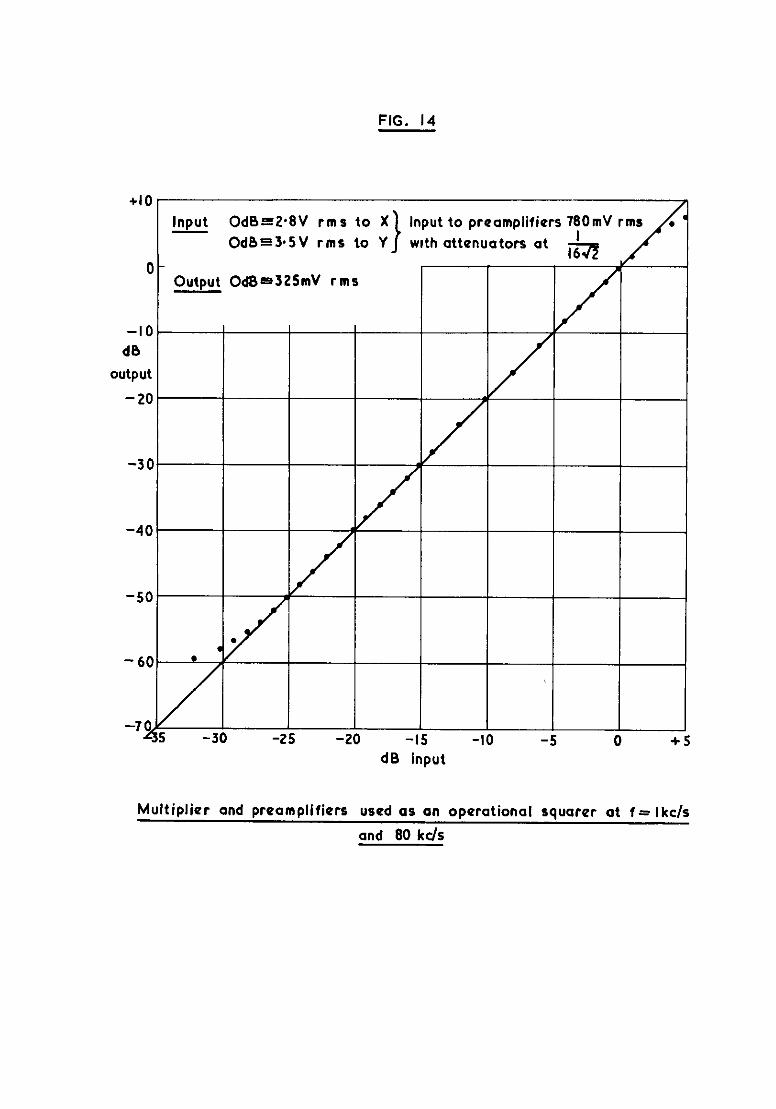
FIG. 14
+I0
0
-10 d0
output
-20
-30
-40
-50
- 60
Input OdB=Z*EV rms to X Input to preamplifiers 780mV rms .
OdBs3*5V rms to Y with attenuators at J
Output OdB=325mV rms r
< I 4
0 -25 -20 -15 - ,I0 dB input
LLl- -5 -5 0 0 + +
Multiplier and preamplifiers used as an operational squarer at f= lkc/s
and 00 kds

I.00 I I I I , I - d -x =I D.C. Y ==A.C. -x- X = A.C. Y = D.C.
I
I I 3
* I I I I I I I
0 10 20 30 40 50 60 80 100 200 300 4 56 Input frequency in kilocycles par second
Frequency response of multiplier
n G) . G
-35 output
dB
-40
-45
-50
-*- X = 2*8V rms Y =0 - Y = 3*ov rms x = 0
output for x = 2.8V rms, Y = 3*OV r ms,= OdB
1 x-
1 I
I 2 3 45 7
Input IO 20
frequency in kilocycles per second 30 40 50 70 100 200
Rejection ratios
FIGS. 17- 2 I
FIG.17
KSrS Mean cube
X 1
FIG. 19
Auto -correlation
FIG. 20
Freauencv analvser
FIG. 21
Sweep frequency generator
Applicatiorm of the multiplier
A.E.C. C.P. NO.685 August, 1962 Johnson, R. F.
A.R.C. C.P. No.685 August, 1962 Johnson, R. F.
A TIAC3-DIVISION ANALOGUE MULTIPLW FOR CORREL4TION A TDIE-DIVISION AI'AZ.OGuE NULTIPLW FOR CORRFLATION bfEAS=TS AND ldXlXG AT FREQUENCIFS UP TO lCEASUREiE?TS AID UXING AT FRFQUENCIES UP TO
loOKILOCYCLE PER SECOND 100 XiLOCYCLZS PER SECOND
A circuit for a tune-dimsion multiplier is descmbed capable of accepting si&s from zero frequency to 103 kc/s. Preamplrfiers and associated circuits are described which enable the multiplier to be used for the measurement of a wise range of parameters encounterea in the turbulence andnoise field.
A cucut for a time-divlsion mltxplier is describe capable of acoeptmg signals from zero frequency to 100 kc/s. Presxplifiers and assocIatea circuits are described whroh enable the multiplier to be used for the measurement of a wide range of parameters encountered in the turbulence and noise fzeld.
A.R.C. C.P. No.685 August, 1962 Johnson, R. F.
A TIME-DIVISION ANALOGUE MULTIPLIER FOR CORRXLATION hO?ASUREMENTS AND NIXLNG AT FlGQUENClES UP TO
100 KILOCYCLES PER SECOND
A ciroult for a tzne-division multipher is described capable of accepting signals from zero frequency to 103 kc/s. Preamplifiers and associated cucuits are described whxh enable the mitt~plier to be used for the measurement of a wide range of parameters encountered zn the turbulence and noue field.


C.P. No. 685
0 Crown copyright 1963
Prmted and pubhshed by
HER MAJKWY’S STATIONERY OFFICE
To be purchased from York House, Kmgsway, London w.c 2
423 Oxford Street, London w.1 13A Castle Street, Edrnburgh 2
109 St Mary Street, Cardtff 39 Kmg Street, Manchester 2
50 Faxfax Street, Bnstol 1 35 Smallbrook, Rmgway, Blmungham 5
80 ChIchester Street, Belfast 1 or through any bookseller
Printed m En&nd
SO. Code No 234013-85
C.P. No. 685