a to d-5204
TRANSCRIPT

8/4/2019 A to D-5204
http://slidepdf.com/reader/full/a-to-d-5204 1/20
ADS5204
SBAS268A – JUNE 2002 – REVISED JULY 2002
Dual 10Bit 40MSPS LowPower
ANALOGTODIGITAL CONVERTER with PGA
PRODUCTION DATA information is current as of publication date. Products conform tospecifications per theterms of TexasInstruments standardwarranty. Production processingdoesnot necessarilyinclude testing of all parameters.
FEATURES
D 3.3V Single-Supply Operation
D Dual Simultaneous Sample-and-Hold Inputs
D Differential or Single-Ended Analog Inputs
D Programmable Gain Amplifier: 0dB to 18dB
D Separate Serial Control Interface
D Single or Dual Parallel Bus Output
D 60dB SNR at fIN = 10.5MHz
D 73dB SFDR at fIN = 10.5MHz
D Low Power: 275mW
D 300MHz Analog Input BandwidthD 3.3V TTL/CMOS-Compatible Digital I/O
D Internal or External Reference
D Adjustable Reference Input Range
D Power-Down (Standby) Mode
D TQFP-48 Package
APPLICATIONSD Digital Communications (Baseband Sampling)
D Portable Instrumentation
D Video Processing
DESCRIPTION
The ADS5204 is a dual 10-bit, 40MSPS Analog-to-Digital
Converter (ADC). It simultaneously converts each analoginput signal into a 10-bit, binary coded digital word up to
a maximum sampling rate of 40MSPS per channel. Alldigital inputs and outputs are 3.3VTTL/CMOS compat-ible.
An innovative dual pipeline architecture implemented in
a CMOS process and the 3.3V supply results in very lowpower dissipation. In order to provide maximum flexibil-
ity, both top and bottom voltage references can be set
from user-supplied voltages. Alternatively, if no externalreferences are available, the on-chip internal refer-ences can be used. Both ADCs share a common refer-
ence to improve offset and gain matching. If externalreference voltage levels are available, the internal refer-ences can be powered down independently from therest of the chip, resulting in even greater power savings.
The ADS5204 also features dual, onboard ProgrammableGain Amplifiers (PGAs) that allow a setting of 0dB to 18dB
to adjust the gain of each set of inputs in order to matchthe amplitude of the incoming signal.
The ADS5204 is characterized for operation from –40°C
to +85°C and is available in a TQFP-48 package.
Please be aware that an important notice concerning availability, standard warranty, and use in critical applications of Texas Instruments
semiconductor products and disclaimers thereto appears at the end of this data sheet.
www.ti.com
Copyright 2002, Texas Instruments Incorporated

8/4/2019 A to D-5204
http://slidepdf.com/reader/full/a-to-d-5204 2/20
ADS5204
SBAS268A – JUNE 2002 – REVISED JULY 2002
www.ti.com
2
ORDERING INFORMATION
PRODUCT PACKAGE–LEADPACKAGE
DESIGNATOR(1)
SPECIFIED
TEMPERATURE
RANGE
PACKAGE
MARKING
ORDERING
NUMBER
TRANSPORT
MEDIA, QUANTITY
ADS5204 TQFP – 48 PFB – 40°C to +85°C AZ5204 ADS5204IPFB Tray, 250
ADS5204 TQFP – 48 PFB – 40°C to +85°C AZ5204 ADS5204IPFBR Tape and Reel, 1000
(1) For the most current specifications and package information, refer to our web site at www.ti.com.
ABSOLUTE MAXIMUM RATINGSover operating free-air temperature range unless otherwise noted(1).
Supply Voltage: AVDD to AGND, DVDD to DGND – 0.5V to 3.6V. . . . . . . . . .
Supply Voltage: AVDD to DVDD, AGND to DGND – 0.5V to 0.5V. . . . . . . . . .
Digital Input Voltage Range to DGND – 0.5V to DVDD + 0.5V. . . . . . . . . . . .
Analog Input Voltage Range to AGND – 0.5V to AVDD + 0.5V. . . . . . . . . . . . .
Digital Output Voltage Applied from Ext. Source to DGND – 0.5V to DVDD + 0.5V. . . . .
Reference Voltage Input Range to AGND: VREFT, VREFB – 0.5V to AVDD + 0.5V. . . . .
Operating Free – Air Temperature Range, TA (ADS5204I) – 40°C to +85°C. .
Storage Temperature Range, TSTG – 65°C to +150°C. . . . . . . . . . . . . . . . . .
Soldering Temperature 1.6mm (1/16 inch) from case for 10 seconds 300°C. . . . . . . . . .
(1)Stresses above these ratings may cause permanent damage. Exposure toabsolute maximum conditions for extended periods may degrade device
reliability. These are stress ratings only, and functional operation of the device
at these or any other conditions beyond those specified is not implied.
This integrated circuit can be damaged by ESD.
Texas Instruments recommends that all
integrated circuits be handled with appropriateprecautions. Failure to observe proper handling and
installation procedures can cause damage.
ESD damage can range from subtle performance degradation
to complete device failure. Precision integrated circuits maybe more susceptible to damage because very small
parametric changes could cause the device not to meet its
published specifications.
RECOMMENDED OPERATING CONDITIONSover operating free-air temperature range, TA, unless otherwise noted.
PARAMETER CONDITIONS MIN NOM MAX UNIT
Power Supply
AVDD
Supply Voltage DVDD 3.0 3.3 3.6 V
DRVDD
Analog and Reference Inputs
Reference Input Voltage (top) VREFT fCLK = 1MHz to 80MHz 1.9 2.0 2.15 V
Reference Input Voltage (bottom) VREFB fCLK = 1MHz to 80MHz 0.95 1.0 1.1 V
Reference Voltage Differential VREFT – VREFB fCLK = 1MHz to 80MHz 0.95 1.0 1.1 V
Reference Input Resistance RREF fCLK = 80MHz 1650 Ω
Reference Input Current IREF fCLK = 80MHz 0.62 mA
Analog Input Voltage, Differential VIN – 1 1 V
Analog Input Voltage, Single – Ended(1) VIN CML – 1.0 CML + 1.0 V
Analog Input Capacitance CI 8 pF
Clock Input(2) 0 AVDD V
Analog Outputs
CML Voltage AVDD /2 V
CML Output Resistance 2.3 kΩ
Digital Inputs
High-Level Input Voltage VIH 2.4 DVDD V
Low-Level Input Voltage VIL DGND 0.8 V
Input Capacitance 5 pF
Clock Period tc (80MHz) 12.5 ns
Pulse Duration tw(CLKH), tw(CLKL) (80MHz) Clock HIGH or LOW 5.25 ns
Clock Period tc (40MHz) 25 ns
Pulse Duration tw(CLKH) , tw(CLKL) (40MHz) Clock HIGH or LOW 11.25 ns
(1) Applies only when the signal reference input connects to CML.(2) Clock pin is referenced to AVDD /AVSS.

8/4/2019 A to D-5204
http://slidepdf.com/reader/full/a-to-d-5204 3/20
ADS5204
SBAS268A – JUNE 2002 – REVISED JULY 2002
www.ti.com
3
ELECTRICAL CHARACTERISTICSover recommended operating conditions with fCLK = 80MHz and use of internal voltage references, and PGA Gain = 0dB, unless otherwise noted.
PARAMETER TEST CONDITIONS MIN TYP MAX UNIT
Power Supply
AVDD 64 72
IDD Operating Supply Current DVDD
AVDD = DVDD = DRVDD = 3.3V,
= p = – 1.7 2.2 mA DRVDD
L = p , IN = . z, – 18 27
pPWDN_REF = ‘L’ 275 345
Power Dissipation PD PWDN_REF = ‘H’ 240 300mW
Standby Power PD(STBY) STDBY = ‘H’, CLK Held HIGH or LOW 95 150 µW
Power-Up Time for All References from Standby tPD 550 ms
Wake Up Time tWU External Reference 40 µs
Digital Inputs
High-Level Input Current on Digital Inputs incl. CLK IIH – 1 +1 µA
Low-Level Input Current on Digital Inputs incl. CLK IILAVDD = DVDD = DRVDD = 3.6V
– 1 +1 µA
Digital Outputs
High-Level Output Voltage VOHAVDD = DVDD = DRVDD = 3.0V at
IOH = 50µA, Digital Outputs Forced HIGH2.8 2.96 V
Low-Level Output Voltage VOLAVDD = DVDD = DRVDD = 3.0V at
IOL= 50µA, Digital Outputs Forced LOW0.04 0.2 V
Output Capacitance CO 5 pF
High-Impedance State Output Current to High – Level IOZH – 1 +1 µA
High-Impedance State Output Current to Low – Level IOZLAVDD = DVDD = DRVDD = 3.6V
– 1 +1 µA
pCLOAD = 10pF, Single-Bus Mode 3 ns
Data Output Rise-and-Fall TimeCLOAD = 10pF, Dual-Bus Mode 5 ns
Reference Outputs
Reference Top Voltage VREFTO Absolute Min/Max Values Valid and 1.9 2 2.1 V
Reference Bottom Voltage VREFBO
Tested for AVDD = 3.3V 0.95 1 1.05 V
Differential Reference Votage REFT – REFB 0.95 1.0 1.05 V
DC Accuracy
Internal ° °Integral Nonlinearity, End Point INLReferences(1) TA = – 40°C to +85°C – 1.5 ±0.4 +1.5 LSB
Differential Nonlinearity DNLInternal
References(2) TA = – 40°C to +85°C – 0.9 ±0.4 +1.0 LSB
Missing Codes No Missing Codes Assured
Zero Error(3) 0.12 ±1.5 %FS
Full-Scale ErrorAVDD = DVDD = DRVDD = 3.3V
3 0.28 ±1.5 %FS
Gain Errorx erna e erences
0.24 ±1.5 %FS
(1) Integral nonlinearity refers to the deviation of each individual code from a line drawn from zero to full-scale. The point used as zero occurs ½LSB
before the first code transition. The full-scale point is defined as a level ½LSB beyond the last code transition. The deviation is measured from
the center of each particular code to the best-fit line between these two endpoints.
(2) An ideal ADC exhibits code transitions that are exactly 1LSB apart. DNL is the deviation from this ideal value. Therefore this measure indicates
how uniform the transfer function step sizes are. The ideal step size is defined here as the step size for the device under test, (i.e., (last transition
level – first transition level)/(2n – 2)). Using this definition for DNL separates the effects of gain and offset error. A minimum DNL better than – 1LSB ensures no missing codes.
(3) Zero error is defined as the difference in analog input voltage —between the ideal voltage and the actual voltage —that will switch the ADC output
from code 0 to code 1. The ideal voltage level is determined by adding the voltage corresponding to ½LSB to the bottom reference level. The
voltage corresponding to 1LSB is found from the difference of top and bottom references divided by the number of ADC output levels (1024).
Full-scale error is defined as the difference in analog input voltage —between the ideal voltage and the actual voltage —that will switch the ADC
output from code 1022 to code 1023. The ideal voltage level is determined by subtracting the voltage corresponding to 1.5LSB from the top
reference level. The voltage corresponding to 1LSB is found from the difference of top and bottom references divided by the number of ADC
output levels (1024).

8/4/2019 A to D-5204
http://slidepdf.com/reader/full/a-to-d-5204 4/20
ADS5204
SBAS268A – JUNE 2002 – REVISED JULY 2002
www.ti.com
4
DYNAMIC PERFORMANCE(1)
TA = TMIN to TMAX, AVDD = DVDD = DRVDD = 3.3V, fIN = – 1dBFS, Internal Reference, fCLK = 80MHz, fS = 40MSPS, Differential Input Range =
2Vp – p, and PGA Gain = 0dB, unless otherwise noted.
PARAMETER TEST CONDITIONS MIN TYP MAX UNIT
Effective Number of Bits ENOB fIN = 3.5MHz 9.7 Bits
fIN = 10.5MHz 9.3 9.7 BitsfIN = 20MHz 9.6 Bits
Total Harmonic Distortion THD fIN = 3.5MHz – 71 dB
fIN = 10.5MHz – 71 – 66 dB
fIN = 20MHz – 68 dB
Signal-to-Noise Ratio SNR fIN = 3.5MHz 60.5 dB
fIN = 10.5MHz 60.5 dB
fIN = 20MHz 60 dB
Signal-to-Noise Ratio + Distortion SINAD fIN = 3.5MHz 60 dB
fIN = 10.5MHz 57 60 dB
fIN = 20MHz 60 dB
Spurious-Free Dynamic Range SFDR fIN = 3.5MHz 75 dB
fIN = 10.5MHz 69 73 dBfIN = 20MHz 70.5 dB
Analog Input Bandwidth See Note (2) 300 MHz
2-Tone Intermodulation Distortion IMD f1 = 9.5MHz, f2 = 9.9MHz – 68 dBc
A/B Channel Crosstalk – 75 dBc
A/B Channel Offset Mismatch 0.016 1.75 % of FS
A/B Channel Full-Scale Error Mismatch 0.025 1.0 % of FS
(1) These specifications refer to a 25Ω series resistor and 15pF differential capacitor between A/B+ and A/B – inputs; any source impedance will
bring the bandwidth down.
(2) Analog input bandwidth is defined as the frequency at which the sampled input signal is 3dB down on unity gain and is limited by the input switch
impedance.
PGA SPECIFICATIONSPARAMETER MIN TYP MAX UNIT
Gain Range 0 to 18 dB
Gain Step Size(1) 0.5826 dB
Gain Error(2) – 0.15 ±0.025 +0.15 dB
Control Bits Per Channel 5 Bits
(1) Refer to Table 2, PGA Gain Code. Ideal step size: 18.0618dB/31 = 0.5826dB(2) Deviation from ideal. Refer to Table 2, all gain settings.
8/4/2019 A to D-5204
http://slidepdf.com/reader/full/a-to-d-5204 5/20
ADS5204
SBAS268A – JUNE 2002 – REVISED JULY 2002
www.ti.com
5
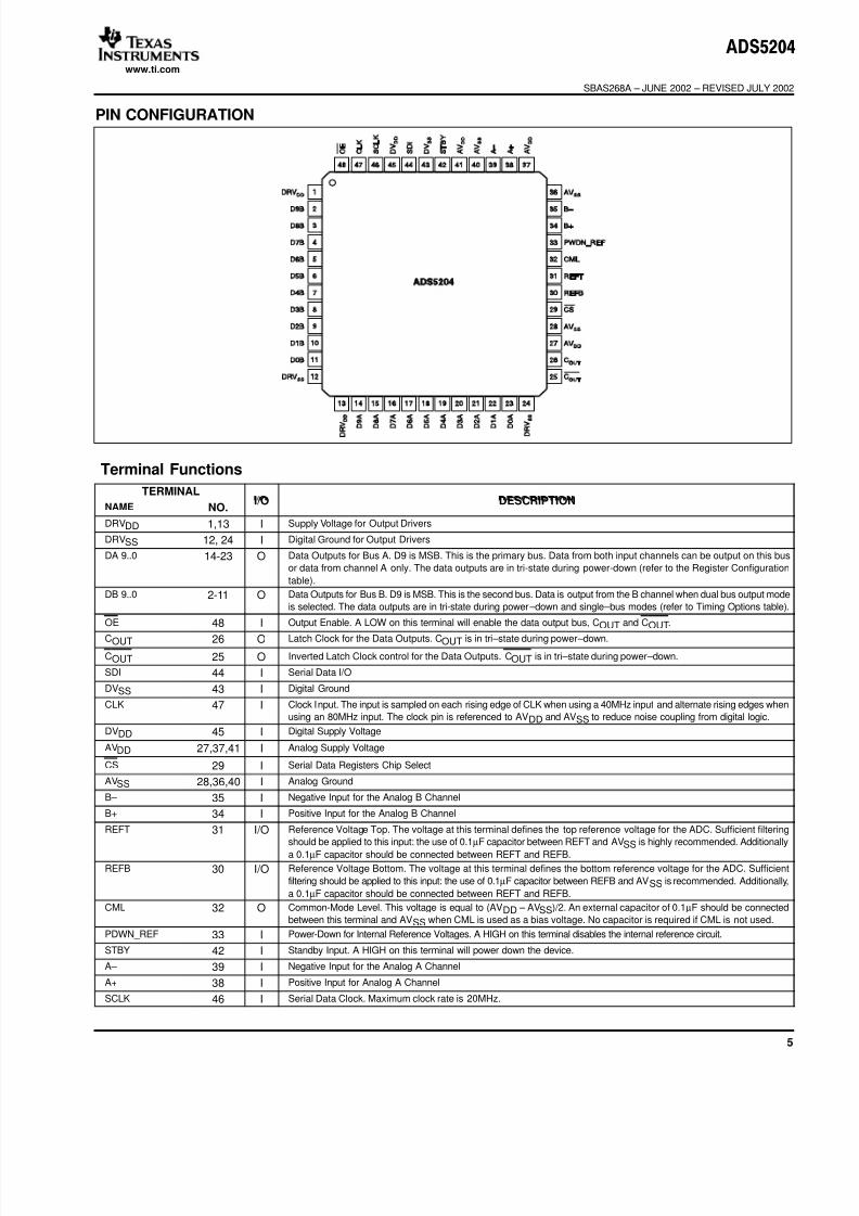
PIN CONFIGURATION
Terminal Functions
TERMINAL
NAME NO.I/O DESCRIPTION
DRVDD 1,13 I Supply Voltage for Output Drivers
DRVSS 12, 24 I Digital Ground for Output Drivers
DA 9..0 14-23 O Data Outputs for Bus A. D9 is MSB. This is the primary bus. Data from both input channels can be output on this bus
or data from channel A only. The data outputs are in tri-state during power-down (refer to the Register Configuration
table).
DB 9..0 2-11 O Data Outputs for Bus B. D9 is MSB. This is the second bus. Data is output from the B channel when dual bus output mode
is selected. The data outputs are in tri-state during power – down and single – bus modes (refer to Timing Options table).
OE 48 I Output Enable. A LOW on this terminal will enable the data output bus, COUT and COUT.
COUT 26 O Latch Clock for the Data Outputs. COUT is in tri – state during power – down.
COUT 25 O Inverted Latch Clock control for the Data Outputs. COUT is in tri – state during power – down.
SDI 44 I Serial Data I/O
DVSS 43 I Digital Ground
CLK 47 I Clock Input. The input is sampled on each rising edge of CLK when using a 40MHz input and alternate rising edges when
using an 80MHz input. The clock pin is referenced to AVDD and AVSS to reduce noise coupling from digital logic.
DVDD 45 I Digital Supply Voltage
AVDD 27,37,41 I Analog Supply Voltage
CS 29 I Serial Data Registers Chip Select
AVSS 28,36,40 I Analog Ground
B – 35 I Negative Input for the Analog B Channel
B+ 34 I Positive Input for the Analog B Channel
REFT 31 I/O Reference Voltage Top. The voltage at this terminal defines the top reference voltage for the ADC. Sufficient filtering
should be applied to this input: the use of 0.1µF capacitor between REFT and AVSS is highly recommended. Additionally
a 0.1µF capacitor should be connected between REFT and REFB.
REFB 30 I/O Reference Voltage Bottom. The voltage at this terminal defines the bottom reference voltage for the ADC. Sufficient
filtering should be applied to this input: the use of 0.1µF capacitor between REFB and AVSS is recommended. Additionally,
a 0.1µF capacitor should be connected between REFT and REFB.
CML 32 O Common-Mode Level. This voltage is equal to (AVDD – AVSS)/2. An external capacitor of 0.1µF should be connected
between this terminal and AVSS when CML is used as a bias voltage. No capacitor is required if CML is not used.
PDWN_REF 33 I Power-Down for Internal Reference Voltages. A HIGH on this terminal disables the internal reference circuit.
STBY 42 I Standby Input. A HIGH on this terminal will power down the device.
A – 39 I Negative Input for the Analog A Channel
A+ 38 I Positive Input for Analog A Channel
SCLK 46 I Serial Data Clock. Maximum clock rate is 20MHz.

8/4/2019 A to D-5204
http://slidepdf.com/reader/full/a-to-d-5204 6/20
ADS5204
SBAS268A – JUNE 2002 – REVISED JULY 2002
www.ti.com
6
TIMING REQUIREMENTS
PARAMETER TEST CONDITIONS MIN TYP MAX UNIT
Input Clock Rate fCLK 1 80 MHz
Conversion Rate 1 40 MSPS
Clock Duty Cycle (40MHz) 45 50 55 %
Clock Duty Cycle (80MHz) 42 50 58 %
Output Delay Time td(o) CL = 10pF 9 14 ns
Mux Setup Time ts(m) 9 10.4 ns
Mux Hold Time th(m) CL = 10pF 1.7 2.1 ns
Output Setup Time ts(o) CL = 10pF 9 10.4 ns
Pipeline Delay (latency, channels A and B) td(pipe) MODE = 0, SELB = 0 8 CLK Cycles
Pipeline Delay (latency, channels A and B) td(pipe) MODE = 1, SELB = 0 4 CLK Cycles
Pipeline Delay (latency, channel A) td(pipe) MODE = 0, SELB = 1 8 CLK Cycles
Pipeline Delay (latency, channel B) td(pipe) MODE = 0, SELB = 1 9 CLK Cycles
Pipeline Delay (latency, channel A) td(pipe) MODE = 1, SELB = 1 8 CLK CyclesPipeline Delay (latency, channel B) td(pipe) MODE = 1, SELB = 1 9 CLK Cycles
Output Hold Time th(o) CL = 10pF 1.5 2.2 ns
Aperture Delay Time td(a) 3 ns
Aperture Jitter tJ(a) 1.5 ps, rms
Disable Time, OE Rising to Hi – Z tdis 5 8 ns
Enable Time, OE Falling to Valid Data ten 5 8 ns
(1) All internal operations are performed at a 40MHz clock rate.
SERIAL INTERFACE TIMINGPARAMETER MIN TYP MAX UNIT
Maximum Clock Rate fSCLK 20 MHz
SCLK Pulse Width HIGH tWH 25 ns
SCLK Pulse Width LOW tWH 25 ns
Setup Time, CS LOW Before First Negative SCLK Edge tSU(CS_CK) 5 ns
CS HIGH Width tWH(CS) 10 ns
Setup Time, 16th Negative SCLK Edge before CS Rising Edge tSU(C16_CK) 5 ns
Setup Time, Data Ready Before SCLK Falling Edge tSU(D) 5 ns
Hold Time, Data Held Valid After SCLK Falling Edge tSU(H) 5 ns
TIMING OPTIONS
OPERATING MODE MODE SELB TIMING DIAGRAM FIGURE
80MHz Input Clock, Dual-Bus Output, COUT = 40MHz 0 0 1
40MHz Input Clock, Dual-Bus Output, COUT = 40MHz 1 0 2
80MHz Input Clock, Single-Bus Output, COUT = 40MHz 0 1 3
80MHz Input Clock, Single-Bus Output, COUT = 80MHz 1 1 4

8/4/2019 A to D-5204
http://slidepdf.com/reader/full/a-to-d-5204 7/20
ADS5204
SBAS268A – JUNE 2002 – REVISED JULY 2002
www.ti.com
7
TIMING DIAGRAMS
Analog_A
Analog_B
DA[9:0]
DB[9:0]
DAB[19:0]
A1 A2 A3 A4 A5
B1 B2 B3 B4 B5
A1 A2 A3 A4 A5
B1 B2 B3 B4 B5
A&B 1 A&B 2 A&B 3 A&B 4 A&B 5
td(pipe)
t
td(o)
td(pipe)
ts(o) th(o)
0 1 2 3 4 5 6 7 8 9 10 11 12 13 14 15 16 17 18
Sample A1 and B1
DAB[19:0] is used to illustrate the placement of the busses DA and DB
ADCOUTA[9:0](3)
ADCOUTB[9:0](3)
COUT
COUT
d(o)
CLK(1)
CLK40INT(2)
NOTES: (1) In this option CLK = 80MHz. (2) CLK40INT refers to 40MHz Internal Clock, per channel. (3) Internal signal only.
Figure 1. Dual Bus Output —Option 1.
Sample A1 and B1
Analog_A
Analog_B
DA[9:0]
DB[9:0]
DAB[19:0]
A1 A2 A3 A4 A5
B1 B2 B3 B4 B5
A1 A2 A3 A4 A5
B1 B2 B3 B4 B5
A&B 1 A&B 2 A&B 3 A&B 4 A&B 5
td(o)
td(o)
ts(o) th(o)
td(pipe)
td(pipe)
8 9 101 2 3 4 5 6 7
DAB[19:0] is used to illustrate the combined busses DA and DB
ADCOUTA[9:0](2)
ADCOUTB[9:0](2)
COUT
COUT
CLK(1)
NOTE: (1) In this option CLK = 40MHz, per channel. (2) Internal signal only.
Figure 2. Dual Bus Output —Option 2.

8/4/2019 A to D-5204
http://slidepdf.com/reader/full/a-to-d-5204 8/20
ADS5204
SBAS268A – JUNE 2002 – REVISED JULY 2002
www.ti.com
8
TIMING DIAGRAMS (Cont.)
Analog_A
Analog_B
DA[9:0]
A1 A2 A3 A4 A5
B1 B2 B3 B4 B5
A1 B1 A2 B2 A3 B3 A4 B4 A5 B5
td(pipe)
td(o)
td(pipe)
td(o)
th(o)
th(o)
ts(o)
ts(o)
0 1 2 3 4 5 6 7 8 9 10 11 12 13 14 15 16 17 18
Sample A1 and B1
ADCOUTA[9:0](3)
ADCOUTB[9:0](3)
COUT
COUT
CLK(1)
CLK40INT(2)
NOTES: (1) In this option CLK = 80MHz. (2) CLK40INT refers to 40MHz Internal Clock, per channel. (3) Internal signal only.
Figure 3. Single Bus Output —Option 1.
Analog_A
Analog_B
DA[9:0]
A1 A2 A3 A4 A5
B1 B2 B3 B4 B5
A1 B1 A2 B2 A3 B3 A4 B4 A5 B5
td(pipe)
td(o)
td(pipe)
td(o)
ts(o)
th(o)
ts(m)
th(m)
0 1 2 3 4 5 6 7 8 9 10 11 12 13 14 15 16 17 18
Sample A1 and B1
ADCOUTA[9:0](3)
ADCOUTB[9:0](3)
COUT
COUT
CLK(1)
CLK40INT(2)
NOTES: (1) In this option CLK = 80MHz. (2) CLK40INT refers to 40MHz Internal Clock, per channel. (3) Internal signal only.
Figure 4. Single Bus Output —Option 2.

8/4/2019 A to D-5204
http://slidepdf.com/reader/full/a-to-d-5204 9/20
ADS5204
SBAS268A – JUNE 2002 – REVISED JULY 2002
www.ti.com
9
TIMING DIAGRAMS (Cont.)
SCLK
CS
SDI
1 2 3 4 15 16
D15 D14 D13 D12 D01 D00D00
tSU(CS_CK)
tSU(D)
tH(D)
tSU(C16_CS)
tWH tWL
tWH(CS)
Figure 5. Serial Data Write.
Table 1. Register Configuration
PGA4
B
15
TWOS
14 13 12 11 10 9 8 7 6 5 4 3 2 1 0
PGA0
A
PGA1
A
PGA2
A
PGA3
A
PGA4
A
PGA1
B
PGA2
B
PGA3
B00
Always write 0
SELBMODEPGA0
BReserved
Default (power-up) condition for this register is all bits = 0.The user register is updated on either the first rising edgeof SCLK after the 16th falling edge or CS rising, whichever
comes first. Raising CS before 16 falling SCLK edgeshave been seen is an incomplete write error and no
register update will occur. The PGA gain settings areresynchronized to the internal data conversion clock toavoid data glitches caused by changing gain settingswhile sampling the inputs.
PGA gain control data is applied to the PGAs on thesecond falling edge of the ADC sample clock
(CLK40INT) after a successful register write. Thisresynchronization ensures that no analog glitch occurs
even when SCLK is asynchronous to CLK.
Note that only the PGA data is resynchronized. TheTWOS, MODE, and SELB register bits take effectimmediately after a successful register write.
OUTPUT DATA FORMATThe output data format can either be in Binary Two’s
Complement ouput mode or in unsigned binary mode,which affects both A and B channels.
TWOS – Binary Two’s Complement Mode:
0 – Unsigned Binary
1 – Binary Two’s Complement Output.

8/4/2019 A to D-5204
http://slidepdf.com/reader/full/a-to-d-5204 10/20
ADS5204
SBAS268A – JUNE 2002 – REVISED JULY 2002
www.ti.com
10
Table 2. PGA DB[0:4], 5 –bit PGA gain code for channel A or B.
GAIN (dB) PGx4 PGx3 PGx2 PGx1 PGx0
0 0 0 0 0 0
0.5606 0 0 0 0 1
1.1599 0 0 0 1 01.6643 0 0 0 1 1
2.3806 0 0 1 0 0
2.8703 0 0 1 0 1
3.5218 0 0 1 1 0
4.0824 0 0 1 1 1
4.6817 0 1 0 0 0
5.1630 0 1 0 0 1
5.8451 0 1 0 1 0
6.3903 0 1 0 1 1
6.9807 0 1 1 0 0
7.6040 0 1 1 0 1
8.0497 0 1 1 1 0
8.7712 0 1 1 1 1
9.2831 1 0 0 0 0
9.8272 1 0 0 0 1
10.4078 1 0 0 1 0
11.0301 1 0 0 1 1
11.7005 1 0 1 0 0
12.0412 1 0 1 0 1
12.7970 1 0 1 1 0
13.2208 1 0 1 1 1
14.0944 1 1 0 0 0
14.5400 1 1 0 0 1
15.0666 1 1 0 1 0
15.5630 1 1 0 1 1
16.1623 1 1 1 0 0
16.7229 1 1 1 0 1
17.4181 1 1 1 1 0
18.0618 1 1 1 1 1

8/4/2019 A to D-5204
http://slidepdf.com/reader/full/a-to-d-5204 11/20
ADS5204
SBAS268A – JUNE 2002 – REVISED JULY 2002
www.ti.com
11
TYPICAL CHARACTERISTICS
At TA = 25°C, AVDD = DVDD = DRVDD = 3.3V, fIN = – 0.5dBFS, Internal Reference, fCLK = 80MHz, fS = 40MSPS, Differential Input Range = 2Vp-p,
25Ω series resistor, and 15pF differential capacitor at A/B+ and A/B – inputs, unless otherwise noted.

8/4/2019 A to D-5204
http://slidepdf.com/reader/full/a-to-d-5204 12/20
ADS5204
SBAS268A – JUNE 2002 – REVISED JULY 2002
www.ti.com
12
TYPICAL CHARACTERISTICS (Cont.)
At TA = 25°C, AVDD = DVDD = DRVDD = 3.3V, fIN = – 0.5dBFS, Internal Reference, fCLK = 80MHz, fS = 40MSPS, Differential Input Range = 2Vp-p,
25Ω series resistor, and 15pF differential capacitor at A/B+ and A/B – inputs, unless otherwise noted.

8/4/2019 A to D-5204
http://slidepdf.com/reader/full/a-to-d-5204 13/20
ADS5204
SBAS268A – JUNE 2002 – REVISED JULY 2002
www.ti.com
13
PRINCIPLE OF OPERATION
The ADS5204 implements a dual high-speed 10-bit,40MSPS converter in a cost-effective CMOS process.The differential inputs on each channel are sampled si-
multaneously. Signal inputs are differential and the clock
signal is single-ended. The clock signal is either 80MHzor 40MHz, depending on the device configuration set by
the user. Powered from 3.3V, the dual-pipeline design ar-chitecture ensures low-power operation and 10-bit resolu-tion. The digital inputs are 3.3V TTL/CMOS compatible.Internal voltage references are included for both bottom
and top voltages. Alternatively, the user may apply exter-nally generated reference voltages. In doing so, the inputrange can be modified to suit the application.
The ADC is a 5-stage pipelined ADC with four stages offully-differential switched capacitor sub-ADC/MDACpairs and a single sub-ADC in stage five. All stages
deliver two bits of the final conversion result. A digitalerror correction is used to compensate for modestcomparator offsets in the sub-ADCs.
SAMPLE-AND-HOLD AMPLIFIER
Figure 6 shows the internal SHA/SHPGA architecture.The circuit is balanced and fully differential for good
supply noise rejection. The sampling circuit has beenkept as simple as possible to obtain good performancefor high-frequency input signals.
Figure 6. SHA/SHPGA Architecture.
The analog input signal is sampled on capacitors CSPand CSN while the internal device clock is LOW. Thesampled voltage is transferred to capacitors CHP and
CHN and held on these while the internal device clockis HIGH. The SHA can sample both single-ended and
differential input signals.
The load presented to the AIN pin consists of theswitched input sampling capacitor CS (approximately
2pF) and its various stray capacitances. A simplifiedequivalent circuit for the switched capacitor input isshown in Figure 7. The switched capacitor circuit ismodeled as a resistor RIN. fCLK is the clock frequency,
which is 40MHz at full speed, and CS is the samplingcapacitor. The use of 25Ω series resistors and a
differential 15pF capacitor at the A/B+ and A/B – inputsis recommended to reduce noise.
NOTE: AIN can be any variationof A or B inputs.
VCM = 0.5 S (V(A/B+) + V(A/B – ))
VCM
fCLK = 40MHz
Figure 7. Equivalent Circuit for the Switched
Capacitor Input.
ANALOG INPUT, DIFFERENTIALCONNECTION
The analog input of the ADS5204 is a differential
architecture that can be configured in various waysdepending on the signal source and the required levelof performance. A fully differential connection willdeliver the best performance from the converter. The
analog inputs must not go below AVSS or above AVDD.The inputs can be biased with any common-mode
voltage provided that the minimum and maximum inputvoltages stay within the range AVSS to AVDD. It is
recommended to bias the inputs with a common-modevoltage around AVDD /2. This can be accomplished
easily with the output voltage source CML, which isequal to AVDD /2. CML is made available to the user tohelp simplify circuit design. This output voltage sourceis not designed to be a reference or to be loaded but
makes an excellent DC bias source and stays wellwithin the analog input common-mode voltage rangeover temperature.

8/4/2019 A to D-5204
http://slidepdf.com/reader/full/a-to-d-5204 14/20
ADS5204
SBAS268A – JUNE 2002 – REVISED JULY 2002
www.ti.com
14
Table 3 lists the digital outputs for the correspondinganalog input voltages.
Table 3. Output Format for Differential Configuration
DIFFERENTIAL INPUT
VIN = (A/B+) – (A/B –), REFT – REFB = 1V, PGA = 0dB
ANALOG INPUT VOLTAGE DIGITAL OUTPUT CODE
VIN = +1V 3FFHVIN = 0 200H
VIN = – 1V 000H
DC-COUPLED DIFFERENTIAL ANALOGINPUT CIRCUIT
Driving the analog input differentially can be achievedin various ways. Figure 8 gives an example where asingle-ended signal is converted into a differential signal
by using a fully differential amplifier such as theTHS4141. The input voltage applied to VOCM of the
THS4141 shifts the output signal into the desiredcommon – mode level. VOCM can be connected to CMLof the ADS5204, the common-mode level is shifted toAVDD /2.
ADS5204
Figure 8. Single –Ended to Differential ConversionUsing the THS4141.
AC-COUPLED DIFFERENTIAL ANALOGINPUT CIRCUIT
Driving the analog input differentially can be achieved by
using a transformer coupling, as illustrated in Figure 9.The center tap of the transformer is connected to the
voltage source CML, which sets the common – modevoltage to AVDD /2. No buffer is required at the output of
CML since the circuit is balanced and no current is drawnfrom CML.
ADS5204
Figure 9. AC-Coupled Differential Input withTransformer.
ANALOG INPUT, SINGLE-ENDEDCONFIGURATION
For a single-ended configuration, the input signal isapplied to only one of the two inputs. The signal appliedto the analog input must not go below AVSS or above
AVDD. The inputs can be biased with any common-modevoltage provided that the minimum and maximum input
voltage stays within the range AVSS to AVDD. It isrecommended to bias the inputs with a common-mode
voltage around AVDD /2. This can be accomplished easilywith the output voltage source CML, which is equal toAVDD /2. An example for this is shown in Figure 10.
ADS5204
Figure 10. AC-Coupled, Single-Ended Configuration.
The signal amplitude to achieve full-scale is 2Vp-p. Thesignal, which is applied at A/B+ is centered at the bias
voltage. The input A/B – is also centered at the biasvoltage. The CML output is connected via a 4.7kΩ
resistor to bias the input signal. There is a directDC – coupling from CML to A/B – while this input is
AC – decoupled through the 10µF and 0.1µF capacitors.The decoupling minimizes the coupling of A/B+ into theA/B – path.

8/4/2019 A to D-5204
http://slidepdf.com/reader/full/a-to-d-5204 15/20
ADS5204
SBAS268A – JUNE 2002 – REVISED JULY 2002
www.ti.com
15
Table 4 lists the digital outputs for the correspondinganalog input voltages.
Table 4. Output Format for Single-Ended Configu-ration.
SINGLE –ENDED INPUT, REFT – REFB = 1V, PGA = 0dB
ANALOG INPUT VOLTAGE DIGITAL OUTPUT CODE
V(A/B+) = VCML + 1V 3FFHV(A/B+) = VCML 200H
V(A/B+) = VCML – 1V 000H
REFERENCE TERMINALS
The ADS5204’s input range is determined by the voltageson its REFB and REFT pins. The ADS5204 has an inter-nal voltage reference generator that sets the ADC refer-ence voltages REFB = 1V and REFT = 2V. The internal
ADC references must be decoupled to the PCB AVSSplane. The recommended decoupling scheme is shownin Figure 11. The common-mode reference voltages
should be 1.5V for best ADC performance.
ADS5204
Figure 11. Recommended External Decoupling forthe Internal ADC Reference.
External ADC references can also be chosen. The
ADS5204 internal references must be disabled by tyingPWDN_REF HIGH before applying the external
reference sources to the REFT and REFB pins. Thecommon-mode reference voltages should be 1.5V for
best ADC performance.
ADS5204
Figure 12. External ADC Reference Configuration.
DIGITAL INPUTS
Digital inputs are CLK, SCLK, SDI, CS, STDBY,
PWDN_REF, and OE. These inputs don’t have apull-down resistor to ground, therefore, they should notbe left floating.
The CLK signal at high frequencies should beconsidered as an ‘analog’ input. CLK should be
referenced to AVDD and AVSS to reduce noise couplingfrom the digital logic. Overshoot/undershoot should be
minimized by proper termination of the signal close tothe ADS5204. An important cause of performancedegradation for a high-speed ADC is clock jitter. Clock
jitter causes uncertainty in the sampling instant of theADC, in addition to the inherent uncertainty on thesampling instant caused by the part itself, as specifiedby its aperture jitter. There is a theoretical relationship
between the frequency (f) and resolution (2N) of a signalthat needs to be sampled on one hand, and on the other
hand the maximum amount of aperture error dtmax thatis tolerable. It is given by the following relation:
dtmax = 1/[π f 2(N+1)]
As an example, for a 10-bit converter with a 20MHz
input, the jitter needs to be kept less than 7.8ps in ordernot to have changes in the LSB of the ADC output due
to the total aperture error.
DIGITAL OUTPUTS
The output of ADS5204 is an unsigned binary or BinaryTwo’s Complement code. Capacitive loading on the
output should be kept as low as possible (a maximumloading of 10pF is recommended) to ensure best
performance. Higher output loading causes higherdynamic output currents and can, therefore, increase
noise coupling into the part’s analog front end. To drivehigher loads, the use of an output buffer isrecommended.
When clocking output data from ADS5204, it isimportant to observe its timing relation to COUT. Please
refer to the timing section for detailed information on thepipeline latency in the different modes.
For safest system timing, COUT and COUT should be used
to latch the output data (see Figures 1 to 4). In Figure 4,COUT can be used by the receiving device to identifywhether the data presently on the bus is from channel Aor B.

8/4/2019 A to D-5204
http://slidepdf.com/reader/full/a-to-d-5204 16/20
ADS5204
SBAS268A – JUNE 2002 – REVISED JULY 2002
www.ti.com
16
LAYOUT, DECOUPLING, AND GROUNDINGRULES
Proper grounding and layout of the PCB on which the
ADS5204 is populated is essential to achieve the statedperformance. It is advised to use separate analog and
digital ground planes that are spliced underneath the IC.
The ADS5204 has digital and analog pins on oppositesides of the package to make this easier. Since there isno connection internally between analog and digital
grounds, they have to be joined on the PCB. It isadvised to do this at one point in close proximity to the
ADS5204.
As for power supplies, separate analog and digital supplypins are provided on the part (AVDD /DVDD). The supply tothe digital output drivers is kept separate as well (DRVDD).
Lowering the voltage on this supply to 3.0V instead of thenominal 3.3V improves performance because of the lowerswitching noise caused by the output buffers.
Due to the high sampling rate and switched-capacitorarchitecture, the ADS5204 generates transients on the
supply and reference lines. Proper decoupling of theselines is, therefore, essential.
SERIAL INTERFACE
A falling edge on CS enables the serial interface,
allowing the 16-bit control register date to be shifted(MSB first) on subsequent falling edges of SCLK. The
data is loaded into the control register on the first risingedge of SCLK after its 16th falling edge or CS rising,whichever occurs first. CS rising before 16 falling SCLK
edges have been counted is an error and the controlregister will not be updated.
The maximum update rate is:
f UPDATEMAX + f SCLK 16+
20 MHz16
+ 1.25 MHz
NOTES
1. Integral Nonlinearity (INL) —Integral nonlinearity
refers to the deviation of each individual code from a linedrawn from zero to full-scale. The point used as zero
occurs ½LSB before the first code transition. The
full-scale point is defined as a level ½LSB beyond the lastcode transition. The deviation is measured from thecenter of each particular code to the true straight line
between these two endpoints.
2. Differential Nonlinearity (DNL) —An ideal ADCexhibits code transitions that are exactly 1LSB apart. DNLis the deviation from this ideal value. Therefore, this
measure indicates how uniform the transfer function stepsizes are. The ideal step size is defined here as the stepsize for the device under test (i.e., (last transition level –
first transition level)/(2n – 2)). Using this definition for DNLseparates the effects of gain and offset error. A minimumDNL better than – 1LSB ensures no missing codes.
3. Zero and Full-Scale Error —Zero error is defined as
the difference in analog input voltage —between theideal voltage and the actual voltage —that will switch theADC output from code 0 to code 1. The ideal voltage
level is determined by adding the voltage correspondingto ½LSB to the bottom reference level. The voltagecorresponding to 1LSB is found from the difference oftop and bottom references divided by the number of
ADC output levels (1024).
Full-scale error is defined as the difference in analog inputvoltage —between the ideal voltage and the actualvoltage —that will switch the ADC output from code 1022to code 1023. The ideal voltage level is determined by
subtracting the voltage corresponding to 1.5LSB from thetop reference level. The voltage corresponding to 1LSB is
found from the difference of top and bottom referencesdivided by the number of ADC output levels (1024).
4. Analog Input Bandwidth —The analog inputbandwidth is defined as the max. frequency of a 1dBFSinput sine that can be applied to the device for which anextra 3dB attenuation is observed in the reconstructed
output signal.
5. Output Timing —Output timing td(o) is measured
from the 1.5V level of the CLK input falling edge to the10%/90% level of the digital output. The digital output
load is not higher than 10pF. Output hold time th(o) ismeasured from the 1.5V level of the COUT input rising
edge to the 10%/90% level of the digital output. Thedigital output is load is not less than 2pF. Aperture delay
td(A) is measured from the 1.5V level of the CLK inputto the actual sampling instant.
The OE signal is asynchronous. OE timing tdis ismeasured from the VIH(MIN) level of OE to thehigh-impedance state of the output data. The digitaloutput load is not higher than 10pF. OE timing ten is
measured from the VIL(MAX) level of OE to the instantwhen the output data reaches VOH(min) or VOL(max) output
levels. The digital output load is not higher than 10pF.
6. Pipeline Delay (latency) —The number of clock
cycles between conversion initiation on an input sampleand the corresponding output data being made
available from the ADC pipeline. Once the data pipelineis full, new valid output data is provided on every clock
cycle. The first valid data is available on the output pinsafter the latency time plus the output delay time td(o)through the digital output buffers. Note that a minimumtd(o) is not guaranteed because data can transition
before or after a CLK edge. It is possible to use CLK forlatching data, but at the risk of the prop delay varyingover temperature, causing data to transition one CLK

8/4/2019 A to D-5204
http://slidepdf.com/reader/full/a-to-d-5204 17/20
ADS5204
SBAS268A – JUNE 2002 – REVISED JULY 2002
www.ti.com
17
cycle earlier or later. The recommended method is touse the latch signals COUT and COUT which aredesigned to provide reliable setup and hold times with
respect to the data out.
7. Wake-Up Time —Wake-up time is from the
power-down state to accurate ADC samples being taken,
and is specified for external reference sources applied tothe device and an 80MHz clock applied at the time ofrelease of STDBY. Cells that need to power up are the
bandgap, bias generator, SHAs, and ADCs.
8. Power-Up Time —Power-up time is from thepower-down state to accurate ADC samples beingtaken with an 80MHz clock applied at the time of release
of STDBY. Cells that need to power up are the bandgap,internal reference circuit, bias generator, SHAs, and
ADCs.
8/4/2019 A to D-5204
http://slidepdf.com/reader/full/a-to-d-5204 18/20
ADS5204
SBAS268A – JUNE 2002 – REVISED JULY 2002
www.ti.com
18
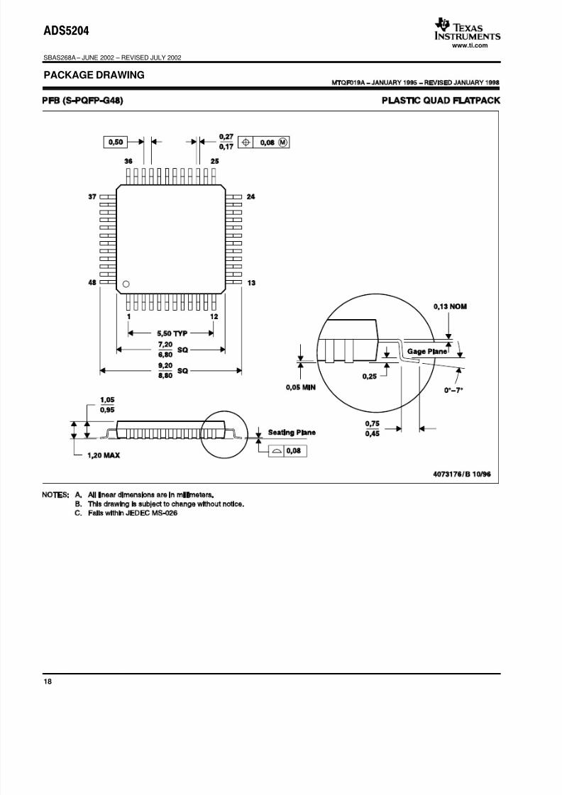
PACKAGE DRAWING

8/4/2019 A to D-5204
http://slidepdf.com/reader/full/a-to-d-5204 19/20
PACKAGING INFORMATION
ORDERABLE DEVICE STATUS(1) PACKAGE TYPE PACKAGE DRAWING PINS PACKAGE QTY
ADS5204IPFB ACTIVE TQFP PFB 48 250
ADS5204IPFBR ACTIVE TQFP PFB 48 1000
(1) The marketing status values are defined as follows:ACTIVE: Product device recommended for new designs.LIFEBUY: TI has announced that the device will be discontinued, and a lifetime-buy period is in effect.NRND: Not recommended for new designs. Device is in production to support existing customers, but TI does not recommend using this part ina new design.PREVIEW: Device has been announced but is not in production. Samples may or may not be available.OBSOLETE: TI has discontinued the production of the device.
PACKAGE OPTION ADDENDUM
www.ti.com 3-Oct-2003
8/4/2019 A to D-5204
http://slidepdf.com/reader/full/a-to-d-5204 20/20