a tri-mode event-based vision sensor with an … tri-mode event-based vision sensor with an embedded...
TRANSCRIPT
A tri-mode event-based vision sensor with anembedded wireless transmitter
Juan A. Lenero-Bardallo1, Wei Tang2, Dongsoo Kim3, Joon Hyuk Park4, and Eugenio Culurciello5
1Nanoelectronics Group, Department of Informatics, University of Oslo, Norway2Klipsch School of Electrical and Computer Engineering, New Mexico State University, USA
3Aptina Imaging Corporation4Department of Electrical Engineering, Yale University, USA
5Weldon School of Biomedical Engineering, Purdue University, USAE-mail: [email protected]
Abstract—We report a vision sensor with three differentoperation modes (intensity, spatial, and temporal contrast), andan integrated UWB wireless transmitter. The sensor is intendedfor surveillance applications in Wireless Sensor Networks (WSN),where autonomous sensor nodes are required. It has event-basedoutput, high dynamic range (120dB), and reduced power con-sumption (we expect less than 2.7mA for the sensor and 10mAfor the wireless transmitter). Its pixels only use 5 transistorsand have a size of 10 × 10µm2, with fill factor of 47%. Thesensor array has 256 × 256 pixels and was implemented inthe standard IBM 8HP SiGe BiCMOS 0.13µm process. In thispaper, we describe the system blocks. Simulation and preliminaryexperimental results are provided.
I. INTRODUCTION
There is a high demand of low-cost and compact vision sys-tems with high dynamic range of operation and reduced outputdata flow. This demand is partially due to the development ofWSNs (Wireless Sensor Networks). Such networks are usedfor plenty of tasks like surveillance, home-care, or industrialapplications [1]–[3]. WSNs require smart autonomous deviceswith reduced power consumption and compressed data flow.These sensors should only send meaningful information to acentral node when necessary. In that sense, devices that detecteither spatial or the temporal contrast, trying to emulate thehuman retina, provide a very reduced data flow, preserving therelevant information to perform recognition. AER (AddressEvent Representation) sensors are quite suitable for WSNsbecause their outputs are typically voltage pulses (events) thatcan be easily conveyed into radio signals and transmittedwirelessly. Several relevant bio-inspired vision sensors withlow power consumption and reduced data flow have beenpublished [4]–[7], but none of them was specifically conceivedto be a WSN autonomous node.
In this paper, we present an improved version of the tri-operation vision sensor presented by D. Kim et al. [8]. Thatsensor had three different operation modes (spatial, temporaland intensity mode), reduced power consumption, and goodfill factor (42%). The new imager has an integrated wirelesstransmitter for its usage in WSNs, higher dynamic range(40dB higher employing dual rolling shutter and a floating
Column Read-out
256x256 Pixel Matrix
Ro
w C
on
tro
l Cir
cuit
Intensity Mode TemporalContrast
Spatial Contrast
ev
ev
+
-
Tran
s. 1
14-bit counter
evev
+-
Controlsignals
Slee
p1
Slee
p2Tr
ans.
2
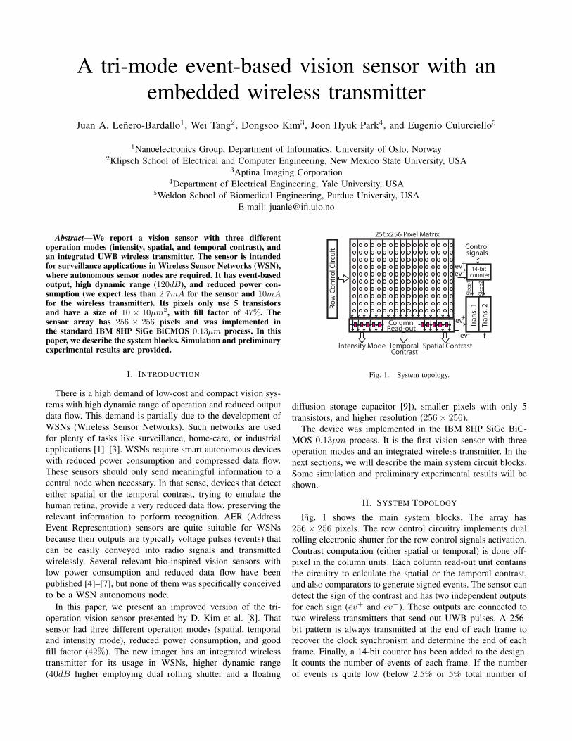
Fig. 1. System topology.
diffusion storage capacitor [9]), smaller pixels with only 5transistors, and higher resolution (256× 256).
The device was implemented in the IBM 8HP SiGe BiC-MOS 0.13µm process. It is the first vision sensor with threeoperation modes and an integrated wireless transmitter. In thenext sections, we will describe the main system circuit blocks.Some simulation and preliminary experimental results will beshown.
II. SYSTEM TOPOLOGY
Fig. 1 shows the main system blocks. The array has256 × 256 pixels. The row control circuitry implements dualrolling electronic shutter for the row control signals activation.Contrast computation (either spatial or temporal) is done off-pixel in the column units. Each column read-out unit containsthe circuitry to calculate the spatial or the temporal contrast,and also comparators to generate signed events. The sensor candetect the sign of the contrast and has two independent outputsfor each sign (ev+ and ev−). These outputs are connected totwo wireless transmitters that send out UWB pulses. A 256-bit pattern is always transmitted at the end of each frame torecover the clock synchronism and determine the end of eachframe. Finally, a 14-bit counter has been added to the design.It counts the number of events of each frame. If the numberof events is quite low (below 2.5% or 5% total number of
SH
RPD
RFD
ROWSEL
C
FD
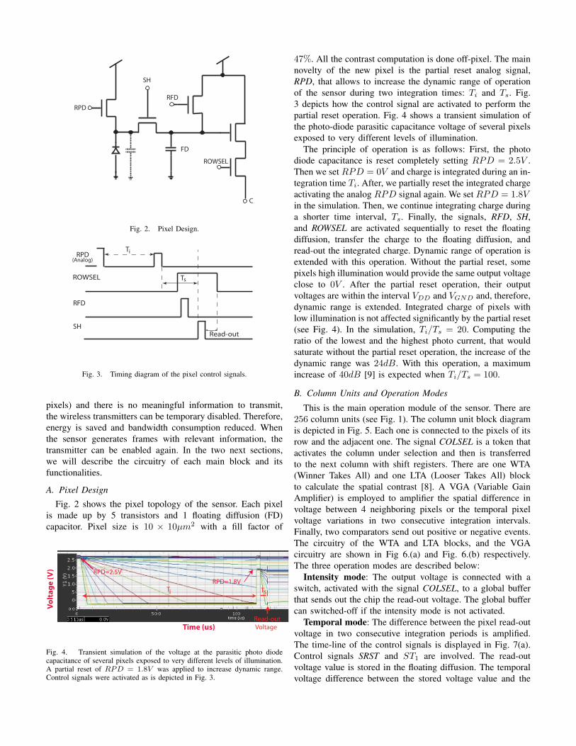
Fig. 2. Pixel Design.
RPD
ROWSEL
RFD
SH
Ti
Ts
(Analog)
Read-out
Fig. 3. Timing diagram of the pixel control signals.
pixels) and there is no meaningful information to transmit,the wireless transmitters can be temporary disabled. Therefore,energy is saved and bandwidth consumption reduced. Whenthe sensor generates frames with relevant information, thetransmitter can be enabled again. In the two next sections,we will describe the circuitry of each main block and itsfunctionalities.
A. Pixel Design
Fig. 2 shows the pixel topology of the sensor. Each pixelis made up by 5 transistors and 1 floating diffusion (FD)capacitor. Pixel size is 10 × 10µm2 with a fill factor of
RPD=1.8VRPD=2.5V
Time (us)
Volt
age
(V)
Read-out Voltage
Ti Ts
Fig. 4. Transient simulation of the voltage at the parasitic photo diodecapacitance of several pixels exposed to very different levels of illumination.A partial reset of RPD = 1.8V was applied to increase dynamic range.Control signals were activated as is depicted in Fig. 3.
47%. All the contrast computation is done off-pixel. The mainnovelty of the new pixel is the partial reset analog signal,RPD, that allows to increase the dynamic range of operationof the sensor during two integration times: Ti and Ts. Fig.3 depicts how the control signal are activated to perform thepartial reset operation. Fig. 4 shows a transient simulation ofthe photo-diode parasitic capacitance voltage of several pixelsexposed to very different levels of illumination.
The principle of operation is as follows: First, the photodiode capacitance is reset completely setting RPD = 2.5V .Then we set RPD = 0V and charge is integrated during an in-tegration time Ti. After, we partially reset the integrated chargeactivating the analog RPD signal again. We set RPD = 1.8Vin the simulation. Then, we continue integrating charge duringa shorter time interval, Ts. Finally, the signals, RFD, SH,and ROWSEL are activated sequentially to reset the floatingdiffusion, transfer the charge to the floating diffusion, andread-out the integrated charge. Dynamic range of operation isextended with this operation. Without the partial reset, somepixels high illumination would provide the same output voltageclose to 0V . After the partial reset operation, their outputvoltages are within the interval VDD and VGND and, therefore,dynamic range is extended. Integrated charge of pixels withlow illumination is not affected significantly by the partial reset(see Fig. 4). In the simulation, Ti/Ts = 20. Computing theratio of the lowest and the highest photo current, that wouldsaturate without the partial reset operation, the increase of thedynamic range was 24dB. With this operation, a maximumincrease of 40dB [9] is expected when Ti/Ts = 100.
B. Column Units and Operation Modes
This is the main operation module of the sensor. There are256 column units (see Fig. 1). The column unit block diagramis depicted in Fig. 5. Each one is connected to the pixels of itsrow and the adjacent one. The signal COLSEL is a token thatactivates the column under selection and then is transferredto the next column with shift registers. There are one WTA(Winner Takes All) and one LTA (Looser Takes All) blockto calculate the spatial contrast [8]. A VGA (Variable GainAmplifier) is employed to amplifier the spatial difference involtage between 4 neighboring pixels or the temporal pixelvoltage variations in two consecutive integration intervals.Finally, two comparators send out positive or negative events.The circuitry of the WTA and LTA blocks, and the VGAcircuitry are shown in Fig 6.(a) and Fig. 6.(b) respectively.The three operation modes are described below:
Intensity mode: The output voltage is connected with aswitch, activated with the signal COLSEL, to a global bufferthat sends out the chip the read-out voltage. The global buffercan switched-off if the intensity mode is not activated.
Temporal mode: The difference between the pixel read-outvoltage in two consecutive integration periods is amplified.The time-line of the control signals is displayed in Fig. 7(a).Control signals SRST and ST1 are involved. The read-outvoltage value is stored in the floating diffusion. The temporalvoltage difference between the stored voltage value and the

C n C n+1
COLSEL
WTA &
LTA
VGA
+ _ + _
V high V
low
ev + ev
_
WTA LTA Tin
Global Buffer
Intensity ModeS1
aS2
aS1
bS2
b
αx(WTA-LTA)
Fig. 5. Column unit block diagram. Each matrix pixel is connected to acolumn unit. This block calculates spatial or temporal contrast.
WTA
LTA
P i,j
SCa
SCa
SC
SC
P i,j+1
P i-1,j
P i-1,j+1
+
_
VdiffVref
C2
C1WTA
LTA
Tin
SC
SC
ST
Vin
SRST
2 bits
(a) (b)
1
1
2
1
1
2
2
b
b
Fig. 6. (a) WTA and LTA blocks and control signals to store the voltageread-out values of four adjacent pixels. (b) VGA circuit and control signalsused to amplifier the difference between the WTA and LTA blocks (spatialcontrast), or the temporal difference between two consecutive pixel outputs(temporal contrast).
latest read-out voltage is amplified with the VGA. This isproportional to the temporal contrast. Each row is selectedand read-out twice in consecutive intervals.
Spatial mode: Spatial contrast is calculated with WTAand LTA operations amplifying the difference of the outputvoltage of 4 neighboring pixels as explained in [8]. The WTAand LTA blocks are used to amplify the difference betweenthe read-out voltage of four adjacent pixels: Pi,j , Pi,j+1,Pi+1,j , and Pi+1,j+1. The control signals SC1a, SC2a, SC1b,SC2b are activated as is depicted on the time-line of Fig. 7.First, the voltage of the selected pixel and the voltage ofits right neighbor are stored at the input capacitors of theWTA and LTA blocks (see Fig 6.(a)). Then, when the nextrow is selected, the voltages of the bottom pixels Pi+1,j ,and Pi+1,j+1 are stored in the same way. Finally, the voltagedifference of the WTA and LTA blocks is amplified with the
(a)
COLSEL
SRTS
ST
SRTS =ST =1, to store the previous pixel value
TEMPORAL MODE
COLSEL
SC a(SC b)
SC a(SC b)
SC
SC
SRST
SPATIAL MODE
For odd rows, operate SC a and SC a
For even rows, operate SC b and SC b
SC =SRST=1 to store the WTA output
SRST=1 to store, SRST=0 to amplify
(b)
T-output
S-output
1
1
1
2
1 1
2
1 2
2 1 2
1
SRTS=0, ST =1 to amplify temporal di�erence1
1
SC =1, SRST=0 to ampli�ty WTA<A di�erence2
Fig. 7. Control signals employed to compute the temporal and the spatialcontrast in the column units.
Baseband PulseGenerator “1”
RF PulseGenerator “1”
Baseband PulseGenerator “0”
RF PulseGenerator “0”
TX Data
TX Clock
TX BB “1”
TX BB “0”
Fig. 8. Block diagram of the non-coherent FSK-OOK wireless transmitter.
VGA. There are two tokens signals to store alternately thevalues of the even and the odd rows.
The VGA outputs are connected to two comparators thatsend out positive or negative events when a positive, Vhigh, ora negative threshold, Vlow are exceeded. The VGA gain can beadjusted with 2 control bits that set the value of the capacitorC2.
C. Wireless Transmitter
Two FSK-OOK transmitters [10] are embedded in the imagesensor to wirelessly send out real-time events in temporal andspatial contrast modes. One transmits the positive event outputev+ and the another one transmits the negative event outputev−. They can be independently disabled or switched off. Bits”1” and ”0” are up-converted to 600MHz and 2GHz, respec-tively with ring oscillators. A time slot is inserted between twoconsecutive bits. The transmitter is shut down automaticallywhen there is no data to send. The received binary data canbe recovered with a non coherent FSK-OOK demodulator. Theadvantage of using FSK-OOK modulation is to achieve clockand data recovery automatically without synchronization. Thewireless unit can transmit data asynchronously so the eventrate can change during communication. A block diagram ofthe transmitter is shown in Fig. 8. The maximum output rate ofthis wireless system is 20Mbps, which is limited by multi pathand environmental noise. Each integrated transmitter occupies
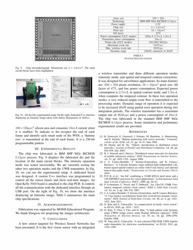
Fig. 9. Chip microphotograph. Dimensions are 4 × 4.2mm2. The maincircuit blocks have been highlighted.
Fig. 10. On the left, experimental setup. On the right, dedicated C++ interfacedisplaying an intensity image taken with indoor illumination of 400lux.
180×120µm2 silicon area and consumes 10mA current whenit is enabled. To indicate to the receptor the end of eachframe and identify each smart node of the WSN, a ’dummyrow’ is transmitted at the end of each frame. It is a 256-bitprogrammable pattern.
III. EXPERIMENTAL RESULTS
The chip was fabricated in IBM 8HP SiGe BiCMOS0.13µm process. Fig. 9 displays the fabricated die and thelocation of the main circuit blocks. The intensity operationmode was tested successfully. We are currently testing theother two operation modes and the UWB transmitter. In Fig.10, we can see the experimental setup. A dedicated boardwas designed. A custom C++ interface was programmed tocontrol all the sensor biases and show real-time images. AnOpal Kelly 3010 board is attached to the chip PCB. It controlsall the communication with the dedicated interface through anUSB port. On the right of Fig. 10, we show the interfacedisplaying an intensity image. Table I summarizes the mainchip specifications.
IV. ACKNOWLEDGMENTS
Fabrication was supported by MOSIS Educational Program.We thank Dongsoo for proposing the imager architecture.
V. CONCLUSIONS
A new sensor targeted for Wireless Sensor Networks hasbeen presented. It is the first vision sensor with an integrated
Array size 256× 256Technology IBM 8HP SiGe BiCMOS 0.13µm
Power supply 2.5VChip size 4× 4.2mm2
Pixel size 10× 10µm2
Fill factor 47%Power consumption (I,S,T, modes) 650µA, 2.7mA, 1.2mA
Transmitter power consumption 10mAFrame rate (I,S,T, modes) 150/800/200fps
Maximum event rate 53MepsMax. wireless event rate 20Meps
Dynamic range 120dB, extension of 40dB
TABLE ISYSTEM SPECIFICATIONS
a wireless transmitter and three different operation modes(intensity mode, and spatial and temporal contrast extraction).It was designed for surveillance applications. Its main featuresare: 256 × 256 pixels resolution, 10 × 10µm2 pixel size, fillfactor of 47%, and low power consumption. Expected powerconsumption is 2.7mA, in spatial contrast mode, and 1.2mA,when computes the temporal contrast. In these two operationmodes, a very reduced output event flow is transmitted to theprocessing nodes. Dynamic range of operation it is expectedto be increased 40dB using partial reset operation during twointegration periods. The wireless transmitter has a maximumoutput rate of 20Meps and a power consumption of 10mA.The chip was fabricated in the standard IBM 8HP SiGeBiCMOS 0.13µm process. Some simulation and preliminaryexperimental results are provided.
REFERENCES
[1] R. Szewczyk, E. Osterweil, J. Polastre, M. Hamilton, A. Mainwaring,and D. Destrin, “Habitat monitoring with sensor networks,” Communi-cations of the ACM, vol. 47, pp. 34–41, June 2004.
[2] M. Duarte and H. Yu, “Vehicle classification in distributed sensornetworks,” Journal of Parallel and Distributed Computing, vol. 64, pp.826–839, July 2004.
[3] R. J. Nemzek and J. Dreicer, “Distributed sensor networks for detectionof mobile radioactive sources,” IEEE Transactions on Nuclear Science,vol. 51, pp. 1693–1701, August 2004.
[4] J. A. Lenero-Bardallo, T. Serrano-Gotarredona, and B. Linares-Barranco, “A 5-decade dynamic range ambient-light-independient cali-brated signed-spatial-contrast aer retina with 0.1ms latency and optionaltime-to-first-spike mode,” Transactions on Circuits and Systems, Part-I,2010.
[5] P.-F. R. et al., “An SoC combining a 132dB QVGA pixel array and a32b DSP/MCU processor for vision applications,” in International SolidState Circuits Conference, ISSCC, 2009, pp. 46–47.
[6] P. Lichtsteiner, C. Posch, and T. Delbruck, “An 128x128 120dB 15us-latency temporal contrast vision sensor,” IEEE J. Solid State Circuits,vol. 43, no. 2, pp. 566–576, 2007.
[7] J. A. Lenero-Bardallo, T. Serrano-Gotarredona, and B. Linares-Barranco,“A 3.6µs latency asynchronous frame-free event-driven dynamic-vision-sensor,” IEEE Journal of Solid-State Circuits, vol. 46, no. 6, pp. 1443–1455, June 2011.
[8] D. Kim and E. Culurciello, “A compact-pixel tri-mode vision sensor,”in ISCAS, 2010, pp. 2434 – 2437.
[9] D. Kim, Y. Chae, J. Cho, and G. Han, “A dual-capture wide dynamicrange CMOS image sensor using floating diffusion capacitor,” IEEETransaction on Electron Devices, vol. 55, no. 10, pp. 2590–2594,October 2008.
[10] W. Tang and E. Culurciello, “A non-coherent FSK-OOK UWB impulseradio transmitter for clock-less synchronization,” in ISCAS, 2011, pp.1295–1298.