a two-chip, 4-mhz, microelectromechanical reference oscillator · pdf file ·...
TRANSCRIPT
A Two-Chip, 4-MHz, Microelectromechanical Reference Oscillator
Krishnakumar Sundaresan, Gavin K. Ho, Siavash Pourkamali and Farrokh Ayazi School of Electrical and Computer Engineering
Georgia Institute of Technology, Atlanta, GA 30332 [email protected], [email protected]
Abstract — The paper describes a 4-MHz temperature compensated reference oscillator based on a capacitive silicon micro-mechanical resonator. The design of the resonator has been optimized to offer large quality factors (22000), while maintaining tunability in excess of 3000ppm for fine tuning and temperature compensation. Oscillations are sustained with a CMOS amplifier and temperature compensation is performed with a novel resonator bias generator. When interfaced with the bias circuit, the oscillator exhibits a temperature drift of 380ppm over a 90ºC range, a 6X improvement in stability over an uncompensated oscillator. The sustaining amplifier and compensation circuitry were fabricated in a 2P3M 0.5µm CMOS process. The oscillator is designed to prototype highly stable, low phase-noise reference oscillators integrated at the chip or package level.
I. INTRODUCTION The reference oscillator is usually one of the hardest
blocks in a system to integrate on Silicon. While quartz crystals offer excellent temperature stability and phase-noise performance, the inability to integrate them with silicon increases the size of systems that rely on clocking schemes. Silicon micromechanical resonators have been proven to offer excellent stability and quality factors in excess of 10000 over a wide range of frequencies [1,2] making them suitable for reference oscillators. The potential for electrostatic tuning of these resonators without using noisy varactor diodes is an attractive option for electronic fine tuning and temperature compensation of the resonant frequency. Further, these devices also offer the possibility of integration at the chip or package level with standard electronics.
While micromechanical resonators have been proven to offer excellent quality factors, the temperature stability of these resonators (typically -25ppm/ºC) [2] is largely inferior to that of quartz. Conventional resonator temperature compensation schemes focus on localized resonator heating or stress compensation techniques [3,4]. The idea of electrostatic compensation is largely unexploited due the need for large voltages, conventionally unavailable in CMOS.
In this work, we demonstrate a 4-MHz electrostatically temperature compensated resonator-oscillator operating with a 5V supply. A voltage multiplier [5] circuit is used to
generate a voltage of approximately 24V; this voltage is applied to a tuning slope generator based on a diode chain to realize a temperature variant bias for the resonator. The oscillation frequency, operating under this bias, drifted by only 380ppm over 90ºC, an improvement of 6X over an uncompensated oscillator.
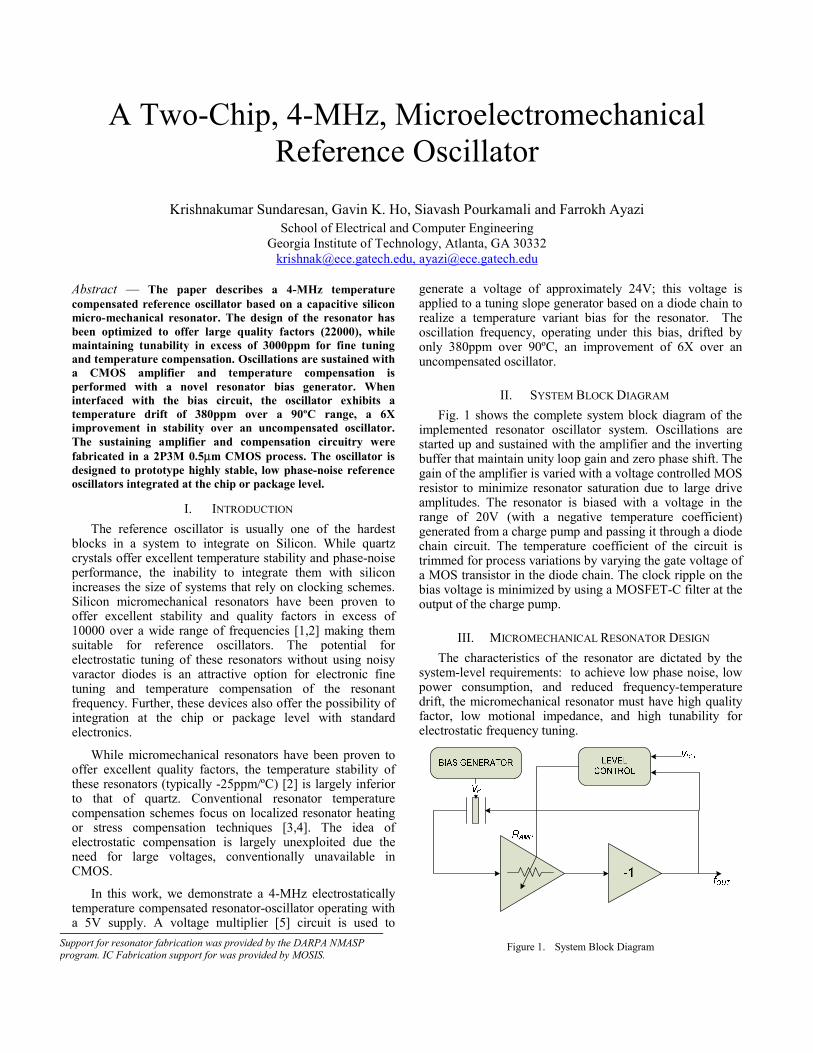
II. SYSTEM BLOCK DIAGRAM Fig. 1 shows the complete system block diagram of the
implemented resonator oscillator system. Oscillations are started up and sustained with the amplifier and the inverting buffer that maintain unity loop gain and zero phase shift. The gain of the amplifier is varied with a voltage controlled MOS resistor to minimize resonator saturation due to large drive amplitudes. The resonator is biased with a voltage in the range of 20V (with a negative temperature coefficient) generated from a charge pump and passing it through a diode chain circuit. The temperature coefficient of the circuit is trimmed for process variations by varying the gate voltage of a MOS transistor in the diode chain. The clock ripple on the bias voltage is minimized by using a MOSFET-C filter at the output of the charge pump.
III. MICROMECHANICAL RESONATOR DESIGN The characteristics of the resonator are dictated by the
system-level requirements: to achieve low phase noise, low power consumption, and reduced frequency-temperature drift, the micromechanical resonator must have high quality factor, low motional impedance, and high tunability for electrostatic frequency tuning.
Figure 1. System Block Diagram Support for resonator fabrication was provided by the DARPA NMASP program. IC Fabrication support for was provided by MOSIS.
These three requirements are typically difficult to achieve simultaneously with a micromechanical resonator. Flexural mode capacitive beam resonators in the frequency of interest are highly tunable, but have high impedances and low Q. Conventional extensional mode capacitive resonators can have high Q and lower impedances, but suffer from low tunability. Piezoelectric resonators are another alternative; they have lower impedances, but no effective tuning technique has been demonstrated for these resonators.
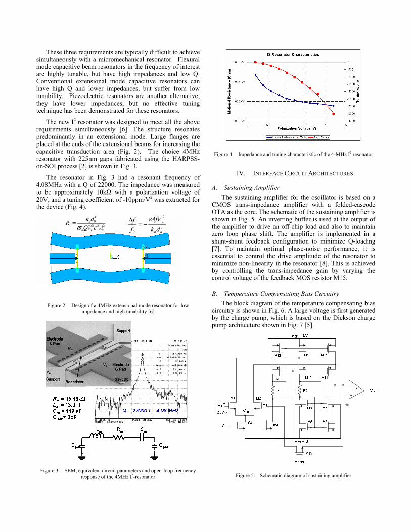
The new I2 resonator was designed to meet all the above requirements simultaneously [6]. The structure resonates predominantly in an extensional mode. Large flanges are placed at the ends of the extensional beams for increasing the capacitive transduction area (Fig. 2). The choice 4MHz resonator with 225nm gaps fabricated using the HARPSS-on-SOI process [2] is shown in Fig. 3.
The resonator in Fig. 3 had a resonant frequency of 4.08MHz with a Q of 22000. The impedance was measured to be approximately 10kΩ with a polarization voltage of 20V, and a tuning coefficient of -10ppm/V2 was extracted for the device (Fig. 4).
Figure 2. Design of a 4MHz extensional mode resonator for low impedance and high tunability [6]
Figure 3. SEM, equivalent circuit parameters and open-loop frequency response of the 4MHz I2-resonator
Figure 4. Impedance and tuning characteristic of the 4-MHz I2 resonator
IV. INTERFACE CIRCUIT ARCHITECTURES
A. Sustaining Amplifier The sustaining amplifier for the oscillator is based on a
CMOS trans-impedance amplifier with a folded-cascode OTA as the core. The schematic of the sustaining amplifier is shown in Fig. 5. An inverting buffer is used at the output of the amplifier to drive an off-chip load and also to maintain zero loop phase shift. The amplifier is implemented in a shunt-shunt feedback configuration to minimize Q-loading [7]. To maintain optimal phase-noise performance, it is essential to control the drive amplitude of the resonator to minimize non-linearity in the resonator [8]. This is achieved by controlling the trans-impedance gain by varying the control voltage of the feedback MOS resistor M15.
B. Temperature Compensating Bias Circuitry The block diagram of the temperature compensating bias
circuitry is shown in Fig. 6. A large voltage is first generated by the charge pump, which is based on the Dickson charge pump architecture shown in Fig. 7 [5].
Figure 5. Schematic diagram of sustaining amplifier
222
40
oPn
nx AQV
dkRεϖ
=3
2
0 ondkAfV
ff P
ε−=∆
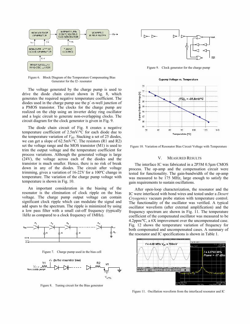
Figure 6. Block Diagram of the Temperature Compensating Bias Generator for the I2- resonator
The voltage generated by the charge pump is used to drive the diode chain circuit shown in Fig. 8, which generates the required negative temperature coefficient. The diodes used in the charge pump use the p+-n-well junction of a PMOS transistor. The clocks for the charge pump are realized on the chip using an inverter delay ring oscillator and a logic circuit to generate non-overlapping clocks. The circuit diagram for the clock generator is given in Fig. 9.
The diode chain circuit of Fig. 8 creates a negative temperature coefficient of 2.5mV/ºC for each diode due to the temperature variation of VBE. Stacking a set of 25 diodes, we can get a slope of 62.5mV/ºC. The resistors (R1 and R2) set the voltage range and the MOS transistor (M1) is used to trim the output voltage and the temperature coefficient for process variations. Although the generated voltage is large (24V), the voltage across each of the diodes and the transistor is much smaller. Hence, there is no risk of break down in any of the diodes. The circuit after voltage trimming, gives a variation of 16-22V for a 100ºC change in temperature. The variation of the charge pump voltage with temperature is shown in Fig. 10.
An important consideration in the biasing of the resonator is the elimination of clock ripple on the bias voltage. The charge pump output voltage can contain significant clock ripple which can modulate the signal and add spurs to the spectrum. The ripple is minimized by using a low pass filter with a small cut-off frequency (typically 1kHz as compared to a clock frequency of 1MHz).
Figure 7. Charge pump used in the bias cell
Figure 8. Tuning circuit for the Bias generator
Figure 9. Clock generator for the charge pump
Figure 10. Variation of Resonator Bias Circuit Voltage with Temperature
V. MEASURED RESULTS The interface IC was fabricated in a 2P3M 0.5µm CMOS
process. The op-amp and the compensation circuit were tested for functionality. The gain-bandwidth of the op-amp was measured to be 175 MHz, large enough to satisfy the gain requirements to sustain oscillations.
After open-loop characterization, the resonator and the IC were interfaced with bond wires and tested under a Desert Cryogenics vacuum probe station with temperature control. The functionality of the oscillator was verified. A typical oscillator waveform (after external amplification) and the frequency spectrum are shown in Fig. 11. The temperature coefficient of the compensated oscillator was measured to be 4.2ppm/ºC, a 6X improvement over the uncompensated case. Fig. 12 shows the temperature variation of frequency for both compensated and uncompensated cases. A summary of the resonator and IC specifications is shown in Table 1.
Figure 11. Oscillation waveform from the interfaced resonator and IC

Figure 12. Temperature variation of compensated and uncompensated resonator-oscillator
TABLE I. SUMMARY OF MEASURED RESULTS
Specification Performance Resonant frequency 4.08 MHz
Unloaded Quality factor 22000 Temperature Coefficient -26.7 ppm/ºC Circuit Specifications
Amplifier Gain Bandwidth product 175 MHz Tuning voltage range (Vclk = 2.5V) 16-22 V
Charge pump clock 1 MHz Ripple filter -3dB frequency 1 kHz
Total power consumption 1.8 mW Oscillator specifications
Frequency variation w/ temperature (25ºC-115ºC) 380ppm
Tuning range 2400 ppm
As we can observe from Fig. 12, the temperature variation of the resonant frequency follows a linear relation. The tuning characteristic with VP is proportional to VP
2 and is given by (1)
3
2
0 on dk
AfVff P
ε−=∆ (1)
where A is the area of the electrode, d0 the electrode gap, f0 is the natural frequency (with zero VP), ∆f the difference between f0 and the operating frequency and kn the stiffness of the resonator. Thus a linear variation of VP with temperature cannot achieve accurate compensation over a wide temperature range. We may notice in fig. 12 that the frequency at the extreme temperatures is almost equal indicating that the compensation technique is optimized over the entire temperature range and further performance gains are difficult. However, with a parabolic compensation voltage described by (2), we can achieve improvements of the order of 50X over the uncompensated oscillator.
BTAVP +=2 (2)
Figure 13. Die picture of fabricated interface IC
A circuit to generate the appropriate temperature profile has been designed and submitted for fabrication. Simulation results indicate an overall variation of 53ppm over -25ºC to 125ºC, a 75X improvement over the uncompensated case.
VI. CONCLUSIONS We have a demonstrated an electronically temperature
compensated reference oscillator based on a high Q micromechanical resonator. The temperature coefficient was measured to be 4.2ppm/ºC, a 6X improvement over an uncompensated oscillator. Techniques to improve the temperature coefficient further have been identified. The oscillator is designed to prototype fully integrated reference oscillators for communication systems.
REFERENCES [1] S. Pourkamali, A. Hashimura, R. Abdolvand, G. K. Ho, A. Erbil, and
F. Ayazi, "High-Q single crystal silicon HARPSS capacitive beam resonators with self-aligned sub-100nm transduction gaps", IEEE/ASME J. MEMS, vol. 12, no. 4, pp. 487-496, August 2003.
[2] S. Pourkamali, Z. Hao and F. Ayazi, "VHF Single Crystal Silicon Capacitive Elliptic Bulk-Mode Disk Resonators—Part II: Implementation and Characterization," IEEE/ASME J. MEMS, vol. 13, no. 6, pp. 1054-1062, Dec. 2004.
[3] W. T. Hsu and C. T.-C. Nguyen, “Geometric stress compensation for enhanced thermal stability in micromechanical resonators,” Proc. of IEEE Intl. Ultrasonics Symposium, pp. 945-948, 1998.
[4] M. Hopcroft et al, “Active temperature compensation for micromachined resonators,” Technical Digest, Solid-state Sensor, Actuator and Microsystems Workshop, June 2004, pp. 364-367.
[5] J. Dickson, “On-chip high-voltage generation in NMOS integrated circuits using an improved voltage multiplier technique,” IEEE J. Solid-State Circuits, vol. 11, no. 6, pp. 374-378, June 1976.
[6] G.K. Ho K. Sundaresan , S. Pourkamali and F. Ayazi “Low-motional-impedance highly-tunable I2 resonators for temperature-compensated reference oscillators,” Proc. of IEEE MEMS 2005, pp. 116-120, Jan 2005.
[7] C.T-C. Nguyen and R.T. Howe, “An integrated high-Q CMOS micromechanical resonator-oscillator,” IEEE J. Solid-State Circuits, vol. 34, no. 4, pp. 440-455, April 1999.
[8] V. Kaajakari, et al, “Nonlinearities in single-crystal silicon micromechanical resonators”, Intl. Conference on Solid-state Sensors, Actuators and Microsystems, pp. 1574-1577, June 2003.