a wireless impedance analyzer for automated tomographic mapping …jerlynch/papers/wireless... ·...
TRANSCRIPT
Smart Structures and Systems, Vol. 8, No. 1 (2011) 139-155 139
A wireless impedance analyzer for automated tomographicmapping of a nanoengineered sensing skin
Sukhoon Pyo1, Kenneth J. Loh2, Tsung-Chin Hou3, Erik Jarva4 and Jerome P. Lynch*1,4
1Dept. of Civil & Environmental Engineering, University of Michigan, Ann Arbor, MI 48109, USA2Dept. of Civil & Environmental Engineering, University of California, Davis, CA 95616, USA
3Dept. of Civil Engineering, National Cheng Kung University(NCKU), Tainan, Taiwan4Dept. of Electrical Engineering & Computer Science, University of Michigan, Ann Arbor, MI 48109, USA
(Received September 1, 2010, Accepted November 28, 2010)
Abstract. Polymeric thin-film assemblies whose bulk electrical conductivity and mechanical performancehave been enhanced by single-walled carbon nanotubes are proposed for measuring strain and corrosionactivity in metallic structural systems. Similar to the dermatological system found in animals, the proposedself-sensing thin-film assembly supports spatial strain and pH sensing via localized changes in electricalconductivity. Specifically, electrical impedance tomography (EIT) is used to create detailed mappings of filmconductivity over its complete surface area using electrical measurements taken at the film boundary. WhileEIT is a powerful means of mapping the sensing skin’s spatial response, it requires a data acquisition systemcapable of taking electrical impedance measurements on a large number of electrodes. A low-cost wirelessimpedance analyzer is proposed to fully automate EIT data acquisition. The key attribute of the device is aflexible sinusoidal waveform generator capable of generating regulated current signals with frequencies fromnear-DC to 20 MHz. Furthermore, a multiplexed sensing interface offers 32 addressable channels from whichvoltage measurements can be made. A wireless interface is included to eliminate the cumbersome wiring oftenrequired for data acquisition in a structure. The functionality of the wireless impedance analyzer is illustrated onan experimental setup with the system used for automated acquisition of electrical impedance measurementstaken on the boundary of a bio-inspired sensing skin recently proposed for structural health monitoring.
Keywords: structural health monitoring; sensing skin; wireless sensor; carbon nanotube; bio-inspired sensing;impedance tomography.
1. Introduction
The United States bridge inventory is rapidly aging with 20% of the nation’s bridges currently
exceeding their intended 50-year design lives; within the next 15 years, it is estimated this number
will exceed 50% (AASHTO 2008). Structural aging is followed by deterioration and the need for
more vigilant structural management. In addition to bridges, many other critical infrastructure systems are
also rapidly aging with significant deterioration reported (ASCE 2009). Current structural health
management methods are based on visual inspection with the inspector looking for visual cues that
may indicate structural distress. While visual inspection is the primary tool for assessing the health
of many complex structural systems such as aircrafts (Melloy et al. 2000), ships (Hess 2007), and
*Corresponding Author, Associate Professor, E-mail: [email protected]

140 Sukhoon Pyo, Kenneth J. Loh, Tsung-Chin Hou, Erik Jarva and Jerome P. Lynch
bridges (Rolander et al. 2001), such methods are known to suffer from a number of limitations.
Specifically, visual inspection is labor-intensive and can be highly subjective (Moore et al. 2001).
To overcome these limitations, researchers in the field of structural health monitoring (SHM) are
developing methods for the autonomous identification of deterioration and damage in structural
systems using permanently installed sensing systems.
Within the SHM field, a particular emphasis has been placed on the development of new sensors
that offer lower costs, reduced form factors, and greater functionality. Among the many technological
developments in the realm of sensors, most notable are the new materials developed for sensing and
actuating structures. In particular, piezoelectric transducers such as lead zirconate titanate (PZT)
have been extensively studied for SHM applications due to their ability to be used as a sensor or
actuator (Park et al. 2003). For example, the electro-mechanical impedance of a PZT patch mounted
to a host structure can be used to detect structural damage. The basic concept of the impedance-
based method is that damage in a structure could be detected by monitoring structural impedance in
a local area using high-frequency vibration (Peairs et al. 2004). Alternative SHM approaches based
on the controlled introduction of high-frequency elastic stress waves in thin plate structural elements
(i.e., Lamb waves) have also been illustrated using PZT pads (Sohn and Kim 2010). In addition to
successful results derived in the laboratory, PZT-based sensing for SHM is also beginning to find its
way to practical settings. For example, PZT-based active damage detection techniques for nondestructive
evaluation of operational steel bridges have been reported (Park et al. 2006).
Other engineered materials under development for SHM include multifunctional, self-sensing
materials that possess electrical properties that are linked to the mechanical and physical properties
of the material (Dharap et al. 2004, Loh and Chang 2010, Loh et al. 2007). Among the many
multifunctional materials under development, carbon nanotube composites have garnered significant
research attention in recent years. Single- and multi-walled carbon nanotubes (SWNT and MWNT,
respectively) have been first reported in the literature by (Iijima 1991). Due to their impressive
mechanical and physical properties (e.g., high tensile strength, high elastic modulus, and large surface
area), the SHM community has explored the inclusion of SWNTs in polymer matrices to create conformable
thin-film sensors for measuring strain (Dharap et al. 2004) and pH (Loh et al. 2007). The inclusion
of SWNTs in the polymer matrix modifies the bulk conductivity of the composite while simultaneously
reinforcing the composite to achieve high tensile strength and stiffness (Loh et al. 2009b).
A distinct advantage of multifunctional materials used for sensing within SHM systems is their
ability to essentially achieve a sensor measurement everywhere the material is. This creates the
opportunity to deviate from the traditional point-based sensing strategies universally used in SHM
systems (i.e., the use of sensors that take localized measurements at a specific point in the structure).
Similar to dermatological systems found in animals, an engineered “sensing skin” possessing
transduction mechanisms throughout its area and deposited on the surface of a structure can serve as a
platform for spatial structural sensing. Using a controlled electrical stimulation and a corresponding
set of voltage measurements taken at the skin boundary, two-dimensional (2D) maps of the skin’s
electrical conductivity can be derived through the use of the electrical impedance tomography (EIT)
technique (Hou et al. 2007). Since thin film conductivity is calibrated to an applied external stimulus
such as strain or pH, conductivity mapping by EIT will yield a corresponding 2D structural damage
map (Loh et al. 2009). However, due to the complexity of the inverse-problem that EIT solves, the
data acquisition requirements of EIT can be challenging to achieve. Specifically, EIT requires a
large number of electrodes mounted to the boundary of the skin, precise control of the direct and
alternating current (DC and AC, respectively) excitation, and repeated injection of electrical current
A wireless impedance analyzer for automated tomographic mapping of a nanoengineered sensing skin 141
on many different electrode pairs (Holder 2005).
A powerful but low-cost approach to EIT data acquisition is proposed herein for bio-inspired thin-
film sensing skins. A wireless impedance analyzer is designed such that any of its 32 channels can
output an electrical current with a user-prescribed frequency, mean, and amplitude, while the remaining
multiplexed channels can measure boundary voltage using an onboard analog-to-digital converter.
Upon data acquisition, an onboard microcontroller provides ample computational resources for
calculating electrical impedance (a complex-valued material property) from the input/output
electrical measurements. Finally, a wireless transceiver is integrated to free the system from its
dependence on coaxial wiring for the communication of electrical impedance data. This portable,
low-cost wireless impedance analyzer is unique in its design when compared to other wireless
impedance analyzers previously proposed for PZT-based SHM (Mascarenas et al. 2007, Park et al.
2009). First, the analyzer proposed in this study supports a large number of channels that are
necessary for EIT; in contrast, previously proposed wireless impedance analyzers have a limited
number of channels (e.g., eight or fewer channels). The wireless impedance analyzer in this study also
has a flexible current generation unit not found in other systems that have relied on a commercial
impedance measurement integrated circuit (i.e., Analog Devices AD5933). The current generation unit
used in the proposed wireless impedance analyzer allows the user to define the electrical current,
whereas analyzers based on the AD5933 hide this functionality from the user and only reports
measured electrical impedance.
This paper begins with an overview of the fabrication and electromechanical characterization of
bio-inspired sensing skins. As mentioned earlier, the sensing skin is a thin conformable film
assembled at the nano-scale using single-walled carbon nanotubes and polyelectrolyte (PE) species.
Similar to skin found in living animals, the thin film can be designed to sense mechanical (i.e.,
strain) and chemical (i.e., corrosion) stimuli in a distributed fashion. Second, the hardware design of
the wireless 32-channel impedance analyzer is presented, including a description of its sensing
interface, computational core, and wireless transceiver. Then, the wireless impedance analyzer is
validated for its ability to interrogate and map the spatial conductivity of SWNT-PE thin films
deposited onto the surface of a steel structure. Specifically, the wireless impedance analyzer will
capture the changes in film conductivity when corrosion occurs in the vicinity of film penetrations
and tears. Finally, the paper concludes with a summary of the key findings and results.
2. Bio-inspired thin-film sensing skin for SHM
Skin is the largest human organ with a cellular design optimized to protect underlying tissue from
the environment (Wilkinson 1998). In particular, skin is a multilayered system consisting of an outer
epidermis layer, a thick inner dermis layer, and a subcutaneous layer. The outer epidermal layer is
comprised of dead cells that are waterproof and designed to be mechanically robust to friction,
tension, and shear. The dermis layer beneath is a sophisticated multi-layered system with a dense
network of neural receptors that provide the skin with its sensing ability. Different receptor types
exist within the dermis neural network to sense touch, temperature, and pain. Human skin is an ideal
basis for bio-inspiration of new SHM sensing technologies for many reasons. First, skin is an
impressive natural multifunctional material system optimized to offer incredible strength (to keep
germs out of the body) while providing distributed sensing capabilities. The intricate neural network
contained within the structure of the skin allows animals to detect the precise location and magnitude of

142 Sukhoon Pyo, Kenneth J. Loh, Tsung-Chin Hou, Erik Jarva and Jerome P. Lynch
stimuli (e.g., touch, heat) in real-time.
A bio-inspired skin system is proposed as a self-sensing coating for metallic structures. The objective
of the sensing skin is to sense the response (i.e., strain) and deterioration (i.e., corrosion) of the
underlying structural system upon which it is placed. Like all natural systems, skin is naturally
fabricated based on a spontaneous self-assembly process that begins at the atomistic scale (Nagayama
1997). For example, nature begins its assembly process with amino acids, which are small molecular
structures that nature uses to assemble proteins. Protein molecules are then used to assemble sub-
cellular components (e.g., organelles) that in turn are used to assemble cells. Cells then self-organize,
reproduce, and form organs and other macro-scale functional elements that are found in all living
beings (Alberts et al. 2008). This self-assembly process is inherently a “bottom-up” approach, which
consists of assembling increasingly complex structured systems from smaller functional blocks. Adopting
a similar approach to bottom-up assembly of engineered materials has become possible with many
of the recent advances in nanotechnology. The controlled assembly of smaller molecular structures to
form complex molecular aggregates at the nano- and micro-scales offers unprecedented opportunities to
achieve desired physical, electrical, and mechanical functionalities at the macro-scale.
In this study, a directed bottom-up assembly method known as layer-by-layer (LbL) is explored
for the fabrication of thin film molecular structures that provide functionality similar to that of
human skin. LbL deposition is a true bottom-up assembly method where supramolecules (i.e.,
polyelectrolyte species) are adsorbed onto the surface of a substrate through non-covalent or
covalent atomic attractions (Fig. 1). Motivation for the adoption of the LbL technique is due to the
fact that this method is low-cost, creates highly homogenous composite materials, and does not
require chemical modification of constituent materials (Decher and Schlenoff 2003). Furthermore,
multi-layered thin films of varying thicknesses can be easily assembled by repeatedly depositing
sets of oppositely charged mono-layers (i.e., bi-layers) (Mamedov et al. 2002). Specifically, SWNT
fillers included in an LbL-assembled poly(vinyl alcohol) (PVA)/poly(sodium 4-styrenesulfonate)
(PSS) thin film will be explored to provide a basis for distributed, multi-modal sensing of physical
phenomena pertinent to structural health monitoring applications. These LbL thin films are referred
to as (SWNT-PSS/PVA)n, where n is the number of bi-layers fabricated.
3. Electrical impedance tomographic mapping
The conductivity of (SWNT-PSS/PVA)n thin films have been shown to vary as a function of strain
Fig. 1 LbL assembly of one bi-layer of the (SWNT-PSS/PVA)50 sensing skin

A wireless impedance analyzer for automated tomographic mapping of a nanoengineered sensing skin 143
(Loh et al. 2007, Loh et al. 2008). This self-sensing attribute of the fabricated thin film can be
leveraged to create strain sensors for SHM applications. However, if the conductivity of the entire
thin film can be mapped, then the film can be utilized as a distributed sensor platform (i.e., sensing
skin) that provides a spatial mapping of strain. To this end, electrical impedance tomography is
adopted to provide a spatial mapping of sensing skin conductivity based on electrical measurements
taken at the skin boundary. The application of EIT to determine changes in sensing skin spatial
conductivity to strain, pH, and tears has been successfully demonstrated in previous studies (Hou et
al. 2007, Loh et al. 2009a).
EIT begins with an analytical model of the flow of electricity in a body (e.g., a multifunctional
thin film) based on an input signal or the injection of a controlled current (either DC or AC) at two
points on the body boundary (Fig. 2). In general, a finite element method (FEM) model describing
electrical flow in the body is formulated from the Laplace vector equation. In the forward problem,
the distribution of body conductivity is known and the analytical model is used to predict the output
electrical potential (i.e., voltage) on the boundary of the body due to the applied current. In contrast,
EIT is an inverse problem in which the distribution of conductivity is unknown and is solved for
using the known input (i.e., injected current) and output (i.e., the boundary electrical potential).
Under one instance of current injection, the current-voltage data set is not sufficient for solving the
underdetermined inverse problem (Holder 2005). Rather, a redundant set of input-output data is
necessary to render the EIT problem tractable. Hence, EIT necessitates stimulation of the body at
multiple locations along the body boundary with corresponding electrical potential measured for each
unique current injection.
The general state-of-practice is to divide the boundary of the body into an equal number of
segments with an electrode placed at the center of each segment. As shown in Fig. 2, the thin film
has 16 electrodes placed equidistantly with four electrodes mounted on each side of the square film.
Fig. 2 EIT data acquisition consists of moving the point of current injection around the thin film boundarywith boundary voltages measured. Each instance of current injection represents one column of theboundary electric potential matrix used in the EIT analysis
144 Sukhoon Pyo, Kenneth J. Loh, Tsung-Chin Hou, Erik Jarva and Jerome P. Lynch
The electrodes are numbered 1 through 16 as shown. First, the current is injected on the 1-2
electrode pair as illustrated in Fig. 2. If the injected current is a DC current, then the electric
potentials, v, are measured on all of the boundary electrode pairs as shown in Fig. 2. If the injected
current is an AC current, then the voltage amplitude and lag (relative to the AC current) are
measured. The measured electric potentials make up the first column of the electric potential matrix,
Φ. Next, the current is applied to the 2-3 electrode pair with the boundary electric potential again
measured. The measured potentials consist of the second column of the electric potential matrix, Φ.
This process repeats until all adjacent electrode pairs have been used to stimulate the thin film. If
done manually, this process can be extremely time-consuming, thereby ruling out the possibility of
employing the sensing skin as an autonomous, real-time SHM system. Therefore, a portable wireless
impedance analyzer is proposed to fully automate EIT data collection in the field setting.
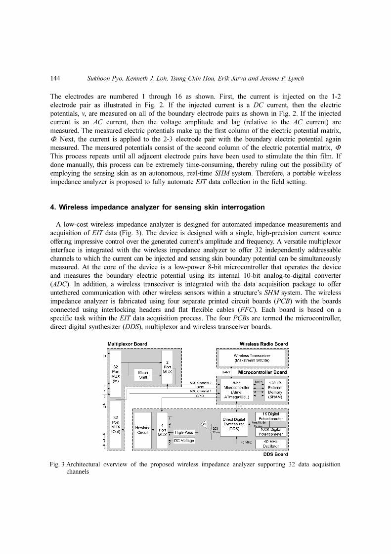
4. Wireless impedance analyzer for sensing skin interrogation
A low-cost wireless impedance analyzer is designed for automated impedance measurements and
acquisition of EIT data (Fig. 3). The device is designed with a single, high-precision current source
offering impressive control over the generated current’s amplitude and frequency. A versatile multiplexor
interface is integrated with the wireless impedance analyzer to offer 32 independently addressable
channels to which the current can be injected and sensing skin boundary potential can be simultaneously
measured. At the core of the device is a low-power 8-bit microcontroller that operates the device
and measures the boundary electric potential using its internal 10-bit analog-to-digital converter
(ADC). In addition, a wireless transceiver is integrated with the data acquisition package to offer
untethered communication with other wireless sensors within a structure’s SHM system. The wireless
impedance analyzer is fabricated using four separate printed circuit boards (PCB) with the boards
connected using interlocking headers and flat flexible cables (FFC). Each board is based on a
specific task within the EIT data acquisition process. The four PCBs are termed the microcontroller,
direct digital synthesizer (DDS), multiplexor and wireless transceiver boards.
Fig. 3 Architectural overview of the proposed wireless impedance analyzer supporting 32 data acquisitionchannels
A wireless impedance analyzer for automated tomographic mapping of a nanoengineered sensing skin 145
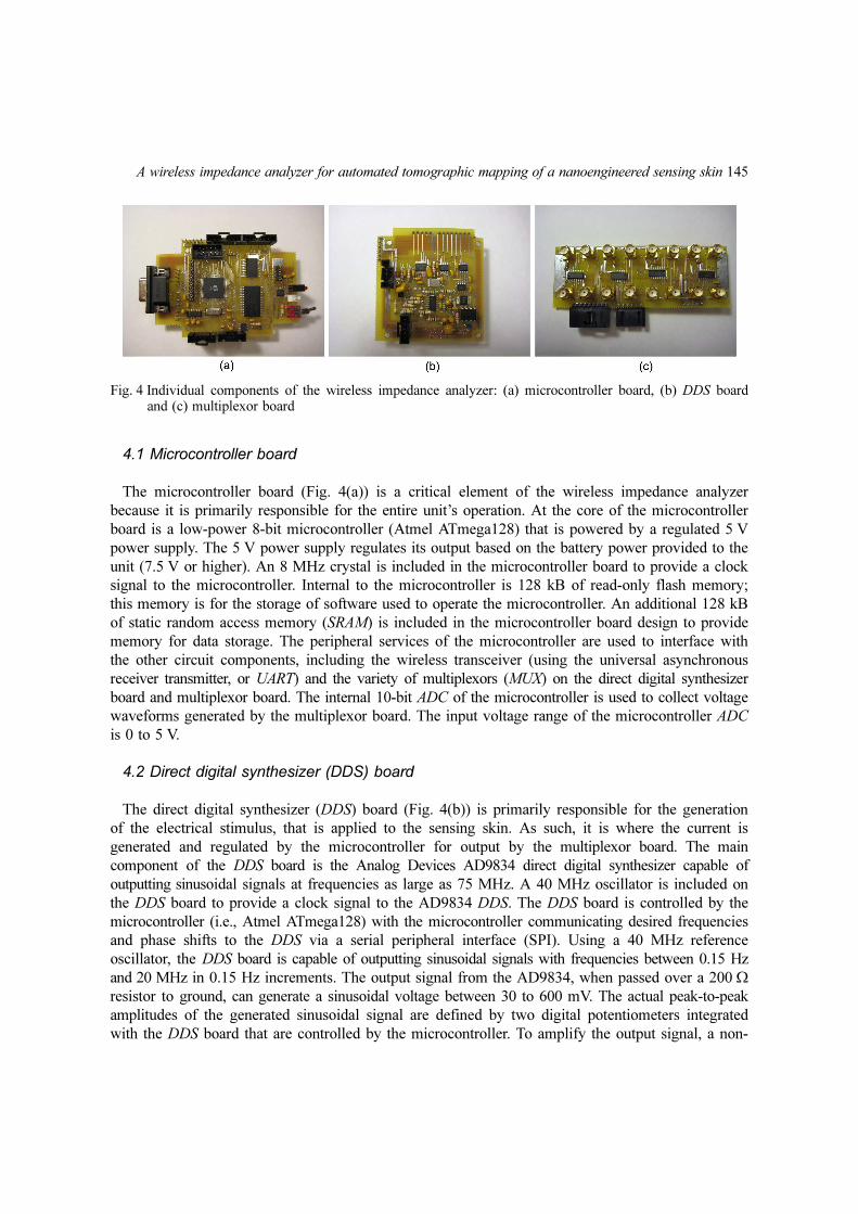
4.1 Microcontroller board
The microcontroller board (Fig. 4(a)) is a critical element of the wireless impedance analyzer
because it is primarily responsible for the entire unit’s operation. At the core of the microcontroller
board is a low-power 8-bit microcontroller (Atmel ATmega128) that is powered by a regulated 5 V
power supply. The 5 V power supply regulates its output based on the battery power provided to the
unit (7.5 V or higher). An 8 MHz crystal is included in the microcontroller board to provide a clock
signal to the microcontroller. Internal to the microcontroller is 128 kB of read-only flash memory;
this memory is for the storage of software used to operate the microcontroller. An additional 128 kB
of static random access memory (SRAM) is included in the microcontroller board design to provide
memory for data storage. The peripheral services of the microcontroller are used to interface with
the other circuit components, including the wireless transceiver (using the universal asynchronous
receiver transmitter, or UART) and the variety of multiplexors (MUX) on the direct digital synthesizer
board and multiplexor board. The internal 10-bit ADC of the microcontroller is used to collect voltage
waveforms generated by the multiplexor board. The input voltage range of the microcontroller ADC
is 0 to 5 V.
4.2 Direct digital synthesizer (DDS) board
The direct digital synthesizer (DDS) board (Fig. 4(b)) is primarily responsible for the generation
of the electrical stimulus, that is applied to the sensing skin. As such, it is where the current is
generated and regulated by the microcontroller for output by the multiplexor board. The main
component of the DDS board is the Analog Devices AD9834 direct digital synthesizer capable of
outputting sinusoidal signals at frequencies as large as 75 MHz. A 40 MHz oscillator is included on
the DDS board to provide a clock signal to the AD9834 DDS. The DDS board is controlled by the
microcontroller (i.e., Atmel ATmega128) with the microcontroller communicating desired frequencies
and phase shifts to the DDS via a serial peripheral interface (SPI). Using a 40 MHz reference
oscillator, the DDS board is capable of outputting sinusoidal signals with frequencies between 0.15 Hz
and 20 MHz in 0.15 Hz increments. The output signal from the AD9834, when passed over a 200 Ω
resistor to ground, can generate a sinusoidal voltage between 30 to 600 mV. The actual peak-to-peak
amplitudes of the generated sinusoidal signal are defined by two digital potentiometers integrated
with the DDS board that are controlled by the microcontroller. To amplify the output signal, a non-
Fig. 4 Individual components of the wireless impedance analyzer: (a) microcontroller board, (b) DDS boardand (c) multiplexor board
146 Sukhoon Pyo, Kenneth J. Loh, Tsung-Chin Hou, Erik Jarva and Jerome P. Lynch
inverting amplifier is designed using standard operational amplifiers to amplify the AD9834 signal
by a factor of five.
To offer the end-user of the wireless impedance analyzer maximum flexibility, the electrical signal
generated by the DDS is split into two parts. First, the sinusoidal signal whose peak-to-peak span is
between 30 to 600 mV (i.e., non-zero mean) is passed to one channel of a 4-channel multiplexor.
The other part of the split is passed through a high-pass filter to remove the non-zero mean. This
high-passed signal is then fed to the second channel of the multiplexor. Finally, a constant voltage is
generated by dividing the 5 V reference of the DDS board using a digital potentiometer for
generating a user-selected voltage that is between 0 and 5 V. This DC voltage is then passed to the
third channel of the multiplexor. The microcontroller is capable of using its general purpose input/
output pins to select which of the three outputs to use (i.e., AC signal with non-zero mean, AC
signal with zero mean, and DC signal). The output of the multiplexor is then fed to a standard
Howland voltage-current converter for output by the DDS board. The maximum permissible current
amplitude capable by the converter is ±5 mA. The output of the Howland circuit is also fed to the
microcontroller ADC and sampled using the ADC’s first input channel.
4.3 Multiplexor board
The multiplexor board is used to output the DDS board’s regulated AC or DC current while
simultaneously recording the corresponding voltage response of the sensing skin (Fig. 4(c)). To ensure
the wireless impedance analyzer can be used for electrical impedance tomography, a large number
of input/output channels are desired. The multiplexor board includes 16 gold plated subminiature
version A (SMA) jacks to which coaxial wires (i.e., electrodes) can be attached. Internally, the
multiplexer board includes four 8-channel multiplexing integrated circuit chips. Two of the 8-channel
multiplexors are used to route the DDS current to any of the board’s 16 electrodes as selected by
the microcontroller using the multiplexors’ select bits. The other two multiplexors are used to feed
the 16 electrode connections to the microcontroller’s 10-bit ADC for sampling. Again, select bits on
the multiplexors are used by the microcontroller to select which electrode it will collect data from
using its ADC. The voltage signal from the multiplexor board is input to the second input channel
of the ADC. If the sensing skin is stimulated by the DDS board with non-zero mean AC or DC
inputs, the recorded voltages will fall within the ADC’s 0 to 5 V input range. However, if the zero
mean AC input is applied to the sensing skin, the voltage generated by the sensing skin will also
have a zero mean. Hence, a voltage mean shift is performed on the multiplexor board to place the
mean of the measured voltage to 2.5 V which falls in the middle of the ADC input voltage range.
Using the applied DDS current as measured on the first ADC channel and electrode voltages measured
on the second ADC channel, the microcontroller can calculate the sensing skin’s impedance based
on amplitude measurements and the relative phase shift between the AC current and measured
voltage.
4.4 Fully assembled device
The microcontroller board includes a set of header pins to accommodate the attachment of the
wireless transceiver that is on its own board (i.e., wireless radio board). The wireless transceiver is a
commercial radio: Maxstream 9XCite digital transceiver. The 9XCite radio operates on the 900
MHz radio band and is capable of data rates as high as 38.4 kbps and a line-of-sight communication

A wireless impedance analyzer for automated tomographic mapping of a nanoengineered sensing skin 147
range of 300 m. The radio is controlled by the microcontroller through a standard UART interface.
The wireless transceiver is connected to the top-side of the microcontroller board. The microcontroller
board is then attached to the DDS board using a set of header pins included in the DDS board
design. The multiplexor board is attached to the microcontroller board using flat flexible cables. A
unique feature of the design of the wireless impedance analyzer is that multiple multiplexor boards
can be included in the assembled device to increase the number of channels. In this study, two
multiplexor boards (16 channels each) are integrated with the wireless impedance analyzer to
accommodate a total of 32 electrodes. The wireless impedance analyzer, when fully assembled (Fig.
5), is 10 cm long, 6 cm wide and 5 cm tall. The device can be powered by standard AC power
available from a standard electrical outlet or can be powered by a 7.5 V battery pack constructed
from five AA batteries.
5. Validation of the wireless impedance analyzer
Two validation experiments are performed to verify the accuracy and reliability of the proposed
wireless impedance analyzer. In the first, the output of the DDS board is analyzed to ensure it is
capable of outputting AC currents with precise amplitudes. The generated AC current is applied to a
1200 Ω resistor, and the corresponding voltage is measured (Fig. 6(a)). In the second, electrical
impedance spectroscopy (EIS) is conducted on a resistor-capacitor (RC) circuit using a four-point
probe method (Fig. 6(b)). The EIS test will analyze the ability of the wireless impedance analyzer to
output an AC current of varying frequency, capture the circuit voltage, and calculate complex-valued
impedance.
5.1 Assessment of DDS board output
The DDS output of the wireless impedance analyzer is analyzed by generating an AC current
applied to a 1.2 kΩ resistor as shown in Fig. 6(a). The amplitude of the DDS board is configured to
be 1 mA peak-to-peak with a non-zero mean. A separate Agilent data acquisition system is attached
to the two terminals of the 1.2 kΩ resistor to record the resistor voltage at a 600 Hz sample rate.
Using Ohm’s Law, the current can be calculated based on the measured voltage. The measured
Fig. 5 Fully assembled wireless impedance analyzer prototype

148 Sukhoon Pyo, Kenneth J. Loh, Tsung-Chin Hou, Erik Jarva and Jerome P. Lynch
voltage signals corresponding to three different AC frequencies (1, 5, and 10 Hz) are shown in Fig. 7.
As shown, the peak-to-peak voltage across the 1.2 kΩ resistor is 1.23 V and corresponds to 1.025 mA
according to Ohm’s Law. Furthermore, the AC frequencies are also measured from the voltage time
histories to be that desired: 1, 5, and 10 Hz.
5.2 Electrical impedance spectroscopy (EIS)
After verifying the accuracy of the DDS board, the ability of the wireless impedance analyzer to
output AC currents of varying frequency and to simultaneously record voltage is assessed. Specifically,
electrical impedance spectroscopy is performed on the RC circuit shown in Fig. 6(b). The wireless
Fig. 6 Validation experiments: (a) assessment of wireless impedance analyzer DDS output using a 1.2 kΩresistor and (b) RC circuit for electrical impedance spectroscopy
Fig. 7 Measured voltage across the 1.2 kΩ resistor due to the applied 1 mA peak-to-peak amplitude AC signalusing three different frequencies: 1 (top), 5 (middle) and 10 Hz (bottom)
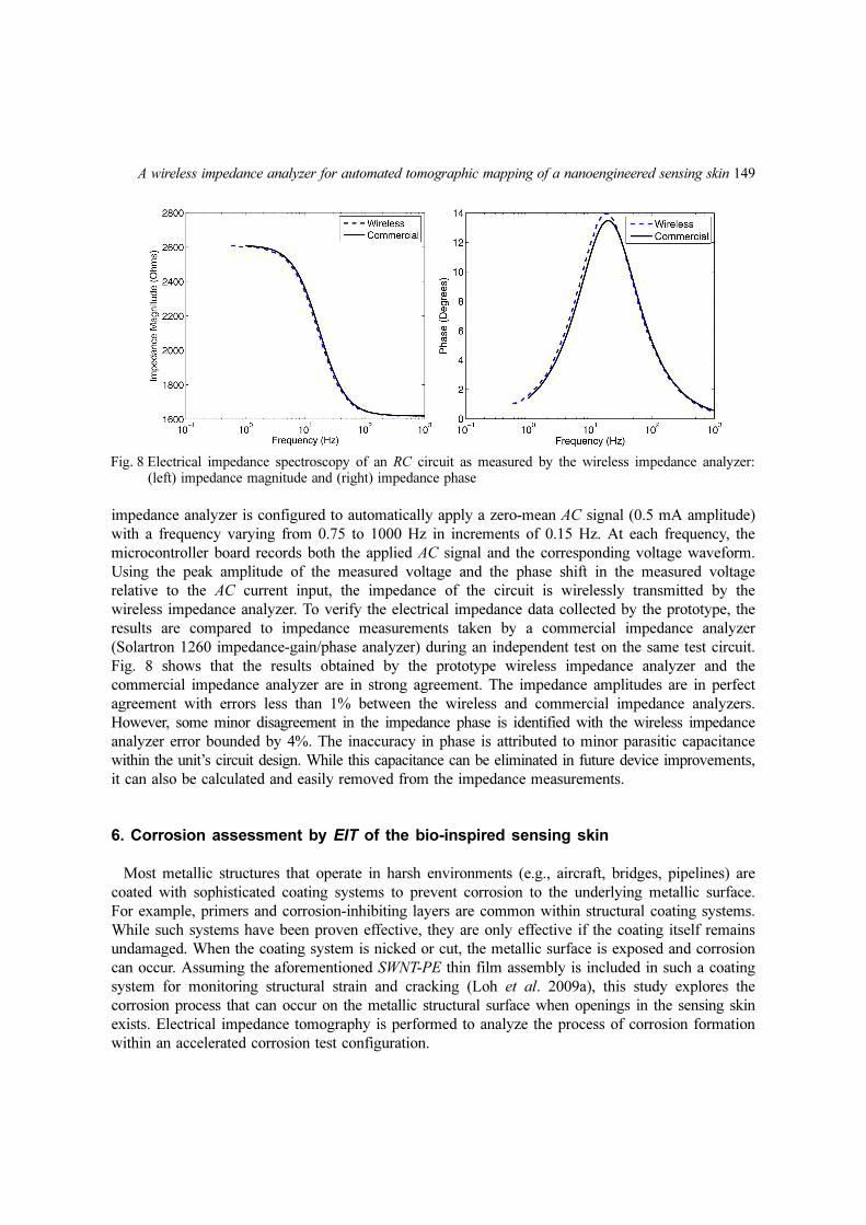
A wireless impedance analyzer for automated tomographic mapping of a nanoengineered sensing skin 149
impedance analyzer is configured to automatically apply a zero-mean AC signal (0.5 mA amplitude)
with a frequency varying from 0.75 to 1000 Hz in increments of 0.15 Hz. At each frequency, the
microcontroller board records both the applied AC signal and the corresponding voltage waveform.
Using the peak amplitude of the measured voltage and the phase shift in the measured voltage
relative to the AC current input, the impedance of the circuit is wirelessly transmitted by the
wireless impedance analyzer. To verify the electrical impedance data collected by the prototype, the
results are compared to impedance measurements taken by a commercial impedance analyzer
(Solartron 1260 impedance-gain/phase analyzer) during an independent test on the same test circuit.
Fig. 8 shows that the results obtained by the prototype wireless impedance analyzer and the
commercial impedance analyzer are in strong agreement. The impedance amplitudes are in perfect
agreement with errors less than 1% between the wireless and commercial impedance analyzers.
However, some minor disagreement in the impedance phase is identified with the wireless impedance
analyzer error bounded by 4%. The inaccuracy in phase is attributed to minor parasitic capacitance
within the unit’s circuit design. While this capacitance can be eliminated in future device improvements,
it can also be calculated and easily removed from the impedance measurements.
6. Corrosion assessment by EIT of the bio-inspired sensing skin
Most metallic structures that operate in harsh environments (e.g., aircraft, bridges, pipelines) are
coated with sophisticated coating systems to prevent corrosion to the underlying metallic surface.
For example, primers and corrosion-inhibiting layers are common within structural coating systems.
While such systems have been proven effective, they are only effective if the coating itself remains
undamaged. When the coating system is nicked or cut, the metallic surface is exposed and corrosion
can occur. Assuming the aforementioned SWNT-PE thin film assembly is included in such a coating
system for monitoring structural strain and cracking (Loh et al. 2009a), this study explores the
corrosion process that can occur on the metallic structural surface when openings in the sensing skin
exists. Electrical impedance tomography is performed to analyze the process of corrosion formation
within an accelerated corrosion test configuration.
Fig. 8 Electrical impedance spectroscopy of an RC circuit as measured by the wireless impedance analyzer:(left) impedance magnitude and (right) impedance phase

150 Sukhoon Pyo, Kenneth J. Loh, Tsung-Chin Hou, Erik Jarva and Jerome P. Lynch
6.1 Experimental details
A carbon steel plate (25 mm wide, 55 mm long, 1.2 mm thick) is selected to serve as the substrate
for the LbL assembly of the SWNT-PSS/PVA thin film. First, the surface of the carbon steel plate is
treated with acetone and ethyl alcohol to rid its surface of impurities and oil. Second, the steel plate
is coated with a thin coat of primer (Krypton General Purpose Primer) to ensure the underlying
steel is electrically isolated from the SWNT-PE thin film assembly. After the primer has been
permitted time to properly dry (72 hr), the LbL process is initiated to form a 50 bi-layer thin film
((SWNT-PSS/PVA)50). Upon film fabrication, eight conductive electrodes are formed along each
side of the film boundary to form a total of 32 electrodes for the entire film. Each electrode is a thin
slice of copper tape bonded to the sensing skin surface by silver paste. Once the silver paste on the
electrodes has dried, the film and primer are mechanically etched on one side of the specimen to
expose two 7 mm circular regions of the bare carbon steel substrate. Finally, a plastic well is then
secured over the exposed circular holes using high-vacuum grease (schematic and photograph of a
specimen are shown in Fig. 9. A coaxial wire is attached to each electrode using an alligator clip
with each of the 32 coaxial wires terminated at the impedance analyzer multiplexor board. The
coaxial cables contain an inner signal line and a grounded sheath that prevents noise from affecting
the signals transmitted over the cable.
Accelerated corrosion of the exposed carbon steel region is conducted by pipetting into plastic
wells #1 and #2 (as denoted in Fig. 9(a)) 0.1 M and 1.0 M sodium chloride solutions, respectively.
These plastic wells are used to confine salt solutions to the selectively etched areas and to promote
corrosion and rust formation at the two circular regions; the plastic wells also serve to prevent the
solutions from wetting other regions of the film. It is known that corrosion of steel occurs due to
the oxidation of iron (within the steel) to form iron oxide (i.e., rust) (Ahmad 2003)
(1a)
(1b)
When water is available for the oxidation of iron, the reaction kinetics highly favors the formation of
iron oxide. As a result, with increased water exposure time, rust will continue to form as long as the
3Fe 4H2O+ Fe3O4 8H+
8e –
+ +→
2Fe 3H2O+ Fe2O3 6H+
6e−
+ +→
Fig. 9 (a) Schematic and (b) photograph show the sensing skin deposited onto a primer-coated carbon steelsubstrate. Two circular regions (i.e., wells #1 and #2) are etched to expose the bare steel substrate foraccelerated corrosion testing

A wireless impedance analyzer for automated tomographic mapping of a nanoengineered sensing skin 151
chemical reaction is not rate-limited by iron availability.
For this validation study, the NaCl solutions are initially pipetted into the plastic wells for 5 min
(herein referred to as the “corrosion time”) and subsequently removed. Then, the specimens are
allowed sufficient time to dry (1 hr) prior to EIT spatial conductivity mapping. The EIT boundary
potential is measured. This procedure completes one sensing skin measurement corresponding to 5
min of corrosion time. Then, fresh 0.1 M and 1.0 M NaCl solutions are again pipetted into the
plastic wells for another 5 min; the procedure is repeated until a total corrosion time of 90 min has
occurred.
6.2 Results and discussion
Upon etching the sensing skin to expose two circular regions of the bare steel substrate, an initial
EIT spatial conductivity map is obtained to serve as the undamaged baseline. For EIT mapping, an
AC current (0.1 mA) with zero mean and 100 Hz frequency is used. Then, following the experimental
details previously outlined, successive time-lapsed EIT maps are acquired for each corrosion time to
Fig. 10 (a) - (h) Set of images at certain corrosion times shows the (left) photograph of the corroded sensingskin-coated specimen as well as the (right) corresponding EIT spatial conductivity maps and (i) Thecolor bar is shown as the negative change in electrical conductivity [S-cm-1]

152 Sukhoon Pyo, Kenneth J. Loh, Tsung-Chin Hou, Erik Jarva and Jerome P. Lynch
monitor the corrosion byproduct formation that results from concentrated sodium chloride solution
exposure. The actual EIT algorithm is performed off-line using a standard personal computer.
Fig. 10 presents the sensing skin spatial conductivity maps (i.e., relative to the baseline) and the
corresponding photographs taken at various corrosion times ranging from 5 to 90 min. It can be
observed that the skin’s electrical conductivity in the vicinity of the wells decrease as corrosion time
increases. The localized decrease in conductivity corresponds to increasing rust (or iron oxide) formation
on the exposed steel surfaces, as is also confirmed by the time-lapsed photographs shown in Fig. 10.
On the other hand, regions outside of the wells that have not been exposed to salt solutions remain
in their pristine state (i.e., no corrosion) throughout the duration of the test. Similarly, the EIT spatial
conductivity maps in Fig. 10 also indicate that the change in conductivity at regions outside the well
are insignificant and are approximately zero. Thus, these results provide evidence that the carbon
nanotube sensing skins employed in this study show potential for spatial corrosion monitoring when
tears and breaks in the sensing skin occurs.
After initially removing the sensing skin and primer at the well locations, the baseline EIT conductivity
map (i.e., pre-corrosion) reveals that the etched regions possess low electrical conductivity and is
significantly less conductive than the thin film. As corrosion takes place and thin layers of
electrically insulating iron oxides form on the steel substrate, the conductivity at the corroded site
should decrease. This hypothesis is consistent with the experimental findings. When the average
negative change in conductivity at wells #1 and #2 are plotted as a function of corrosion time, an
exponential decrease in well conductivity is obtained as shown in Fig. 11. With increasing salt
solution exposure time, the average negative conductivity change for both wells #1 (1.0 M NaCl
solution) and #2 (0.1 M NaCl solution) follow the same trend; initially, a sudden drop in conductivity
is observed, followed by a decreasing rate until it plateaus at t = 90 min. The plateau effect is due to
the fact that the area of bare steel (or iron availability) decreases with increasing iron oxidation and
rust formation. The results obtained in Fig. 11 agree with those obtained by Yonemoto and Shida
(1998) where they have determined that their proposed corrosion sensor’s impedance increases in a
Fig. 11The average conductivity at each well is computed and plotted as a function of corrosion time, and theresults are fitted to an exponential decay model

A wireless impedance analyzer for automated tomographic mapping of a nanoengineered sensing skin 153
similar fashion with increasing rust thickness. In fact, the experimental results obtained in Fig. 11
can be easily fit to an exponential decay model of the form –∆σ=-Ae-Bt+C via regression analysis.
Results from numerical fitting suggest that the average change in thin film conductivity due to
corrosion byproduct formation is well-behaved. The nanocomposite conductivity decreases at an
exponential rate of 0.031 min-1 for well #1 (1.0 M NaCl) and 0.024 min-1 for well #2 (0.1 M NaCl).
The faster corrosion rate for well #1 is consistent with the higher concentration of salt solution
employed during testing.
7. Conclusions
In previous studies, it has already been shown that carbon nanotube-based thin films change their
electrical properties in response to applied strain or pH (Hou et al. 2007, Loh et al. 2009). Unlike
traditional sensors based on data measurements at a discrete point, these thin films can be employed
as a distributed sensor platform (or sensing skin). Electrical impedance tomography utilizes boundary
electrical measurements for mapping thin film spatial conductivity; however, due to the complexity
of the EIT inverse problem, multiple sets of boundary current injection and potential measurements
are required. Realization of a real-time and autonomous SHM system demands an alternative solution
for rapid automated EIT data collection. Thus, a wireless impedance analyzer is designed and proposed
for automated impedance measurements and for the acquisition of electrical impedance tomography
data. Unlike other wireless impedance analyzers, the user can selectively output an electrical current of
controlled amplitude and frequency (i.e., from near-DC to 20 MHz) at any one of its 32 independently
addressable channels, while the device samples voltage at the remaining electrodes. All the
measurements are controlled by a low-power 8-bit microcontroller, and its internal 10-bit ADC
digitizes the acquired data. The data collected can be stored in an onboard 128 kB SRAM, but data
communication to a centralized data repository is ultimately achieved with a Maxstream 9XCite
wireless transceiver integrated with the device hardware. The fully assembled unit is 10 cm long, 6 cm
wide, and 5 cm tall and can draw its power from an AC electrical source or from a 7.5V battery pack.
Upon hardware implementation, three tests have been performed to validate the wireless impedance
analyzer’s impedance and EIT data acquisition performance. First, the device is commanded to
interrogate a 1.2 kΩ resistor using 1 mA AC current outputs at three different AC frequencies (1, 5,
and 10 Hz), while the voltage response is measured by the wireless unit and a tethered Agilent data
acquisition system. The results obtained show that the wireless impedance analyzer is capable of
generating electrical signals at prescribed amplitudes and frequencies. For the second test, the wireless
impedance analyzer is connected to an RC circuit for conducting electrical impedance spectroscopy.
The device applies a zero-mean AC signal from 0.75 to 1000 Hz while the corresponding voltage
magnitude and phase is recorded at each applied AC frequency for computing the impedance of the
RC circuit. When compared to the results obtained by a commercial Solartron 1260 impedance
analyzer, good agreement and low measurement errors are confirmed. Finally, electrical impedance
tomography is employed for spatial conductivity mapping of a (SWNT-PSS/PVA)50 thin film
deposited onto a primer-coated steel plate. The objective is to identify localized changes in thin film
conductivity when concentrated salt solutions accelerate corrosion and rust formation at exposed
metallic structural surface areas. It has been shown that the EIT spatial conductivity maps show
localized decreases in conductivity corresponding to rust (or iron oxide) formation. On the other
hand, the sensing skin’s conductivity remains fairly constant at other locations where there is no

154 Sukhoon Pyo, Kenneth J. Loh, Tsung-Chin Hou, Erik Jarva and Jerome P. Lynch
corrosion activity. Thus, these results validate the use of EIT for mapping thin film spatial
conductivity, and the wireless impedance analyzer provides a more cost effective and rapid method
for EIT data acquisition.
Acknowledgements
This research is supported by the National Science Foundation under Grant Number CMMI-
0846256 (Program Manager: Dr. S.C. Liu). The authors would also like to gratefully acknowledge
additional support offered by the U.S. Department of Commerce, National Institute of Standards and
Technology (NIST) Technology Innovation Program (TIP) under Cooperative Agreement Number
70NANB9H9008.
References
AASHTO. (2008), “Bridging the gap: restoring and rebuilding the nation’s bridges”, American Association ofState Highway and Transportation Officials, Washington D.C.
Ahmad, S. (2003), “Reinforcement corrosion in concrete structures, its monitoring and service life prediction - areview”, Cement Concrete Comp., 25(4-5), 459-471.
Alberts, B., Johnson, A., Lewis, J., Raff, M., Roberts, K. and Walter, P. (2008), Molecular Biology of the Cell,Garland Science, Taylor & Francis Group, New York, NY.
ASCE. (2009), “Report card for america’s infrastructure”, American Society of Civil Engineers, Reston, VA.Decher, G. and Schlenoff, J.B. (2003), “Multilayer thin films”, Wiley-VCH, Weinheim, Germany.Dharap, P., Li, Z., Nagarajaiah, S. and Barrera, E.V. (2004), “Nanotube film based on single-wall carbon nanotubes
for strain sensing”, Nanotechnology, 15(3), 379-382.Hess, P.E. “Structural health monitoring for high-speed naval ships”, Proceedings of the 6th International
Workshop on Structural Health Monitoring, Stanford, CA, 3-15.Holder, D.S. (2005), Electrical Impedance Tomography - Methods, History and Applications, Institue of Physics
Publishing, Bristol, UK.Hou, T.C., Loh, K.J. and Lynch, J.P. (2007), “Spatial conductivity mapping of carbon nanotube composite thin
films by electrical impedance tomography for sensing applications”, Nanotechnology, 18(31), 315501.Iijima, S. (1991), “Helical microtubules of graphitic carbon”, Nature, 354(6348), 56-58.Loh, K.J. and Chang, D. (2010), “Zinc oxide nanoparticle-polymeric thin films for dynamic strain sensing”, J.
Mater. Sci., Online First, 1-10.Loh, K.J., Hou, T.C., Lynch, J.P. and Kotov, N.A. (2009a), “Carbon nanotube sensing skins for spatial strain and
impact damage identification”, J. Nondestruct. Eval., 28(1), 9-25.Loh, K.J., Kim, J., Lynch, J.P., Kam, N.W.S. and Kotov, N.A. (2007), “Multifunctional layer-by-layer carbon
nanotube-polyelectrolyte thin films for strain and corrosion sensing”, Smart Mater. Struct., 16(2), 429-438.Loh, K.J., Lynch, J.P., Shim, B.S. and Kotov, N. (2008), “Tailoring piezoresistive sensitivity of multilayer carbon
nanotube composite strain sensors”, J. Intel. Mat. Syst. Struct., 19(7), 747-764.Loh, K.J., Thouless, M.D. and Lynch, J.P. (2000b), “Enhancing the mechanical and fracture properties of
nanocomposites using carbon nanotubes”, Proceedings of the12th International Conference on Fracture, Ottawa,Canada.
Mamedov, A.A., Kotov, N.A., Prato, M., Guldi, D., Wicksted, J. and Hirsch, A. (2002), “Molecular design ofstrong SWNT/polyelectrolyte multilayers composites”, Nat. Mater., 1(3), 190-194.
Mascarenas, D.L., Todd, M.D., Park, G. and Farrar, C.R. (2007), “Development of an impedance-based wirelesssensor node for structural health monitoring”, Smart Mater. Struct., 16(6), 2137-2145.
Melloy, B.J., Harris, J.M. and Gramopadhye, A.K. (2000), “Predicting the accuracy of visual search performancein the structural inspection of aircraft”, Int. J. Ind. Ergonom., 26(2), 277-283.

A wireless impedance analyzer for automated tomographic mapping of a nanoengineered sensing skin 155
Moore, M., Phares, B., Graybeal, B., Rolander, D. and Washer, G. (2001), “Reliability of visual inspection for
highway bridges”, FHWA-RD-01-020, Federal Highway Administration, Washington D.C.
Nagayama, K. (1997), “Self-assembly: naturés way to do it.”, Royal Institution Discourses Series, Vega ScienceTrust, London, England.
Park, G., Sohn, H., Farrar, C.R. and Inman, D.J. (2003), “Overview of piezoelectric impedance-based healthmonitoring and path forward”, Shock Vib., 35(6), 451-463.
Park, S., Park, S.K., Shin, H.H. and Yun, C.B. (2009), “Wireless sensor self-diagnosis for piezoelectric actuating/sensing networks”, Proceedings of the SPIE - The International Society for Optical Engineering, San Diego, CA,72920B.
Park, S., Yun, C.B., Roh, Y. and Lee, J.J. (2006), “PZT-based active damage detection techniques for steel bridgecomponents”, Smart Mater. Struct., 15(4), 957-966.
Peairs, D.M., Park, G. and Inman, D.J. (2004), “Improving accessibility of the impedance-based structural healthmonitoring method”, J. Intel. Mat. Syst. Struct., 15(2), 129-139.
Rolander, D.D., Phares, B.M., Graybeal, B.A., Moore, M.E. and Washer, G.A. (2001), “Highway bridge inspection:state-of-the-practice survey”, Transport. Res. Record, 1749(1), 73-81.
Sohn, H. and Kim, S.B. (2010), “Development of dual PZT transducers for reference-free crack detection in thinplate structures”, IEEE T. Ultrason. Ferr., 57(1), 229-240.
Wilkinson, J.D. and Shaw, S. (1998), Dermatology, Churchill Livingston, Edinburgh, UK.Yonemoto, N. and Shida, K. (1998), “Multi-functional sensing for high-sensitivity detection of initial state of iron
rust”, Proceedings of the IEEE Instrumentation and Measurement Technology Conference, St. Paul, MN,1145-1148.