aalborg universitet autonomous voltage unbalance
TRANSCRIPT
Aalborg Universitet
Autonomous Voltage Unbalance Compensation in an Islanded Droop-ControlledMicrogrid
Savaghebi, Mehdi; Jalilian, Alireza ; Vasquez, Juan Carlos; Guerrero, Josep M.
Published in:I E E E Transactions on Industrial Electronics
DOI (link to publication from Publisher):10.1109/TIE.2012.2185914
Publication date:2013
Document VersionEarly version, also known as pre-print
Link to publication from Aalborg University
Citation for published version (APA):Savaghebi, M., Jalilian, A., Vasquez, J. C., & Guerrero, J. M. (2013). Autonomous Voltage UnbalanceCompensation in an Islanded Droop-Controlled Microgrid. I E E E Transactions on Industrial Electronics, 60(4),1390-1402. https://doi.org/10.1109/TIE.2012.2185914
General rightsCopyright and moral rights for the publications made accessible in the public portal are retained by the authors and/or other copyright ownersand it is a condition of accessing publications that users recognise and abide by the legal requirements associated with these rights.
- Users may download and print one copy of any publication from the public portal for the purpose of private study or research. - You may not further distribute the material or use it for any profit-making activity or commercial gain - You may freely distribute the URL identifying the publication in the public portal -
Take down policyIf you believe that this document breaches copyright please contact us at [email protected] providing details, and we will remove access tothe work immediately and investigate your claim.
1
1 Abstract—Recently, there is an increasing interest in using
distributed generators (DGs) not only to inject power into the grid, but also to enhance the power quality. In this paper, a stationary-frame control method for voltage unbalance compensation in an islanded microgrid is proposed. This method is based on the proper control of DGs interface converters. The DGs are controlled to compensate voltage unbalance autonomously while share the compensation effort and also active and reactive power, properly. The control system of the DGs mainly consists of active and reactive power droop controllers, virtual impedance loop, voltage and current controllers and unbalance compensator. The design approach of the control system is discussed in detail and simulation and experimental results are presented. The results demonstrate the effectiveness of the proposed method in compensation of voltage unbalance.
Index Terms—Distributed generator (DG), microgrid, voltage unbalance compensation.
I. INTRODUCTION BALANCED voltages can result in adverse effects on equipment and power system. Under unbalanced
conditions, the power system will incur more losses and be less stable. Also, voltage unbalance has some negative impacts on equipment such as induction motors, power electronic converters and adjustable speed drives (ASDs). Thus, the International Electrotechnical Commission (IEC) recommends the limit of 2% for voltage unbalance in electrical systems [1].
A major cause of voltage unbalance is the connection of unbalanced loads (mainly, single-phase loads connection between two phases or between one phase and the neutral).
Compensation of voltage unbalance is usually done using series active power filter through injection of negative sequence voltage in series with the distribution line [2]-[4].
Manuscript received April 30, 2011. Accepted for publication January 9,
2012. Copyright © 2012 IEEE. Personal use of this material is permitted.
However, permission to use this material for any other purposes must be obtained from the IEEE by sending a request to pubs-
[email protected] M. Savaghebi and A. Jalilian are with the Electrical Engineering
Department and Center of Excellence for Power System Automation and Operation, Iran University of Science and Technology, Tehran 16846-13114, Iran (e-mails: [email protected], [email protected]).
J. C. Vasquez is with the Institute of Energy Technology, Aalborg University, Aalborg East DK-9220, Denmark (e-mail: [email protected]).
J. M. Guerrero is with the Institute of Energy Technology, Aalborg University, Aalborg East DK-9220, Denmark and the Department of Automatic Control and Industrial Informatics, Technical University of Catalonia (UPC), 08036 Barcelona, Spain (e-mail: [email protected]).
However, there are a few works [5]-[9] based on shunt compensation to mitigate voltage unbalance. In these works, voltage unbalance caused by unbalanced load is compensated through balancing the line currents. But, in the case of severe load unbalance the amplitude of the current injected by active filter can be very high and exceed the filter rating.
On the other hand, it is well-known that the Distributed Generators (DGs) often consist of a prime mover connected through an interface converter (e.g. an inverter in the case of dc/ac conversion) to the ac power distribution system. The distribution system may be the utility grid or the local grid formed by a cluster of DGs which is called microgrid. The main role of DG inverter is to adjust output voltage phase angle and amplitude in order to control the active and reactive power injection. In addition, compensation of power quality problems can be achieved through proper control strategies [10]. In [11]-[14], some approaches are presented to use the DG for voltage unbalance compensation.
The control method presented in [11] and [12] is based on using a two-inverter structure one connected in shunt and the other in series with the grid, like a series-parallel active power filter [15]. The main role of the shunt inverter is to control active and reactive power flow, while the series inverter balances the line currents and the voltages at sensitive load terminals, in spite of unbalanced grid voltage. This is done by injecting negative sequence voltage. Thus, two inverters are necessary for the power injection and unbalance compensation. It can be considered as a negative point, especially in terms of the cost and volume of the DG interface converter.
A method for voltage unbalance compensation through injection of negative sequence current by the DG has been proposed in [13]. By applying this method, line currents become balanced in spite of the unbalanced loads presence. However, under severely unbalanced conditions, a large amount of the interface converter capacity is used for compensation and it may interfere with the active and reactive power supply by the DG.
The approach presented in [14] is based on controlling the DG as a negative sequence conductance to compensate the voltage unbalance in a microgrid. In this approach which is implemented in the synchronous ( )dq reference frame, compensation is done by generating a reference for negative sequence conductance based on the negative sequence reactive power. Then, this conductance is applied to produce the
Autonomous Voltage Unbalance Compensation in an Islanded Droop-Controlled Microgrid
Mehdi Savaghebi, Student Member, IEEE, Alireza Jalilian, Juan C. Vasquez, and Josep M. Guerrero, Senior Member, IEEE
U
2
compensation reference current. In [14] the compensation reference is injected at the output of the voltage control loop. However, such compensation will be considered as a disturbance to be rejected by the voltage control loop. In the other words, there is a trade-off between the unbalance compensation efficiency and voltage regulation adequacy.
To cope with this problem, the present paper proposes the direct change of the voltage reference to compensate voltage unbalance in a microgrid. This way, the compensation reference is considered as a command to be followed by the voltage controller. Also, since no design approach is presented in [14], the details of the control system design are discussed.
In the proposed method, the overall control system is designed in the stationary ( )αβ reference frame. The main control loops are as follows: • Voltage and current controllers • Virtual impedance loop • Active and reactive power controllers • Voltage unbalance compensator
This paper is organized as follows. The DG interface inverter control strategy is discussed in Section II. In this Section the details of the whole control structure are explained. Section III is dedicated to the design of the control system. Simulation and experimental results are presented in Section IV. Finally, the paper is concluded in Section V.
II. DG INTERFACE CONVERTER (INVERTER) CONTROL METHOD
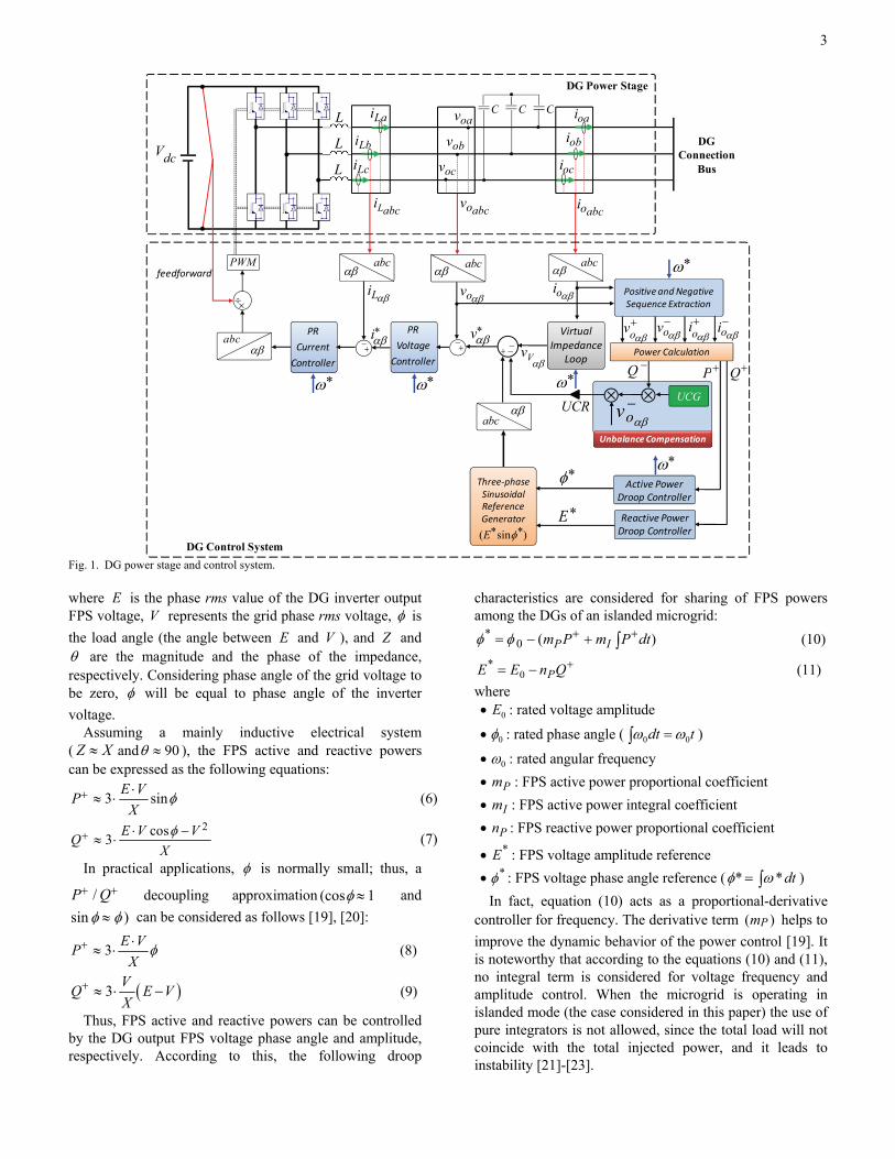
Fig. 1 shows the power stage of a DG and the proposed control strategy for its interface inverter. The power stage consists of a dc prime-mover ( dcV ), an inverter and an LC filter.
As mentioned before, the control system of Fig. 1 is designed inαβ reference frame. So, the Clarke transformation is used to transform the variables between abc andαβ frames. The equations (1) and (2) are used for the transformation:
1 112 2 23 3 30
2 2
abcx xαβ
⎡ ⎤− −⎢ ⎥⎢ ⎥= ⋅⎢ ⎥
−⎢ ⎥⎣ ⎦
(1)
1 0
2 1 33 2 2
1 32 2
abcx xαβ
⎡ ⎤⎢ ⎥⎢ ⎥⎢ ⎥= − ⋅⎢ ⎥⎢ ⎥⎢ ⎥− −⎢ ⎥⎣ ⎦
(2)
where abc
x and xαβ can represent the instantaneous output
voltage (abcov
and ov
αβ), output current (
abcoi and oi αβ
) or
LC filter inductor current (abcLi
and Li αβ) in abc and αβ
frames, respectively:
abc
a
b
c
xx x
x
⎡ ⎤⎢ ⎥= ⎢ ⎥⎢ ⎥⎣ ⎦
, x
xx
α
αβ
β
⎡ ⎤⎢ ⎥
= ⎢ ⎥⎢ ⎥⎣ ⎦
The three-phase instantaneous voltages are measured with respect to an artificial null voltage ( nv ) which is calculated as follows:
3ab bc ca
nv v v
v+ +
= (3)
where abv , bcv and cav represent the instantaneous phase-to-phase voltages.
As seen in (1) and (2), the stationary frame is formed by α and β components and zero component is not considered. It should be noted that in the present paper, a three-phase three-wire islanded microgrid is considered. Since, zero sequence current cannot flow in the three-wire ungrounded electrical systems [16]; zero sequence voltage drops will not affect the system voltages. Also, zero sequence which may be present in the main grid voltages has no effect on an islanded microgrid. Generally, zero sequence voltage cannot be present in the three-wire electrical systems in the absence of a fault (e.g. phase-to-ground short circuit) [17], [18].
As shown in Fig. 1, the voltage controller follows the references generated by power controllers and unbalance compensation block and generates the reference for the current controller. The output of the current controller is transformed back to abc frame and then divided by dcV to provide three-phase voltage reference for the pulse width modulator (PWM). Finally, the PWM block controls the switching of the inverter based on this reference. It is noteworthy that dcV is not constant. Thus, a feedforward loop is included to consider dcV value for generation of the gate signals. This way, variations of dcV inside the allowed limits can be compensated.
In Fig. 1, *ω is the reference angular frequency of the microgrid. In fact, active and reactive power controllers provide the references of DG voltage phase angle (frequency) and amplitude in order to ensure proper parallel operation of the DGs. As explained in Subsection II-A, it is done by using phase angle and amplitude droop controllers.
More details about the control system are presented in the following Subsections.
A. Active and Reactive Power Control Considering a three-phase DG which is connected to the
grid through the impedance Z θ∠ , the fundamental positive sequence (FPS) active and reactive powers injected to the grid by the DG ( P+ and Q+ , respectively) can be expressed as follows [19]:
23 cos cos 3 sin sinE V V E VP
Z Z Zφ θ φ θ+ ⎛ ⎞⋅ ⋅
= ⋅ − + ⋅⎜ ⎟⎜ ⎟⎝ ⎠
(4)
23 cos sin 3 sin cosE V V E VQ
Z Z Zφ θ φ θ+ ⎛ ⎞⋅ ⋅
= ⋅ − − ⋅⎜ ⎟⎜ ⎟⎝ ⎠
(5)
3
*αβv*
αβi
obvoav
−αβoi
Lai oai
abcαβ
abcαβ
PR
Voltage
Controller
abcαβ
Virtual Impedance
Loop
abcαβ Power Calculation
abcαβ
Positive and Negative Sequence Extraction
DG Control System
−αβov +
αβoi+αβov
−αβov
UCG⊗
−Q
⊗
Unbalance Compensation
+P +Q
dcVobi
oci
L
L
L
Lbi
Lci ocv
+ −
Active Power Droop Controller
−
Reactive Power Droop Controller
*E
PWM
*φ
αβoiαβovαβLi
CC
DG Power Stage
DG Connection
Bus
abcoiabcovabcLi
C
+−+
PR
Current
Controller
−
UCR
*ω*ω *ω
*ω
*ω
αβVv
Three‐phase Sinusoidal Reference Generator
)*sin*( φE
×÷
feedforward
Fig. 1. DG power stage and control system.
where E is the phase rms value of the DG inverter output FPS voltage, V represents the grid phase rms voltage, φ is the load angle (the angle between E and V ), and Z and θ are the magnitude and the phase of the impedance, respectively. Considering phase angle of the grid voltage to be zero, φ will be equal to phase angle of the inverter voltage.
Assuming a mainly inductive electrical system ( XZ ≈ and 90≈θ ), the FPS active and reactive powers can be expressed as the following equations:
3 sinE VPX
φ+ ⋅≈ ⋅ (6)
2cos3 E V VQX
φ+ ⋅ −≈ ⋅ (7)
In practical applications, φ is normally small; thus, a
/P Q+ + decoupling approximation 1(cos ≈φ and )sin φφ ≈ can be considered as follows [19], [20]:
3 E VPX
φ+ ⋅≈ ⋅ (8)
( )3 VQ E VX
+ ≈ ⋅ − (9)
Thus, FPS active and reactive powers can be controlled by the DG output FPS voltage phase angle and amplitude, respectively. According to this, the following droop
characteristics are considered for sharing of FPS powers among the DGs of an islanded microgrid:
∫ ++ +−= )(0* dtPmPm IPφφ (10)
+−= QnEE P0*
(11) where • 0E : rated voltage amplitude
• 0φ : rated phase angle ( tdt 00 ωω =∫ )
• 0ω : rated angular frequency • Pm : FPS active power proportional coefficient • Im : FPS active power integral coefficient • Pn : FPS reactive power proportional coefficient
• *E : FPS voltage amplitude reference • *φ : FPS voltage phase angle reference ( * *dtφ ω= ∫ )
In fact, equation (10) acts as a proportional-derivative controller for frequency. The derivative term ( )Pm helps to improve the dynamic behavior of the power control [19]. It is noteworthy that according to the equations (10) and (11), no integral term is considered for voltage frequency and amplitude control. When the microgrid is operating in islanded mode (the case considered in this paper) the use of pure integrators is not allowed, since the total load will not coincide with the total injected power, and it leads to instability [21]-[23].
4
The design of the droop controllers is sufficiently studied in the literature (e.g. [19]-[22]) and will not be discussed in the present paper.
As it can be seen in Fig. 1, *E and *φ are used to generate the three phase reference voltages of the inverter. These voltages are FPS components; thus FPS powers (P+ and Q+) are used in equations (10) and (11). According to Fig. 1, in order to calculate these powers, at first DG three-phase instantaneous output voltage and current (
abcov and
abcoi , respectively) are measured and transformed to αβ
frame (αβov
and
αβoi , respectively). Then, instantaneous
values of fundamental positive and negative sequence output voltage ( +
αβov and −
αβov , respectively) and output
current ( +αβoi and −
αβoi , respectively) are extracted [24],
[25] and fed to power calculation block. It is noteworthy that according to the symmetrical
components theory [26] any set of the unbalanced three-phase quantities (e.g. voltages or currents) can be resolved into three sets of balanced sequence components, namely positive, negative and zero sequence components. Positive sequence components consist of three phasors with equal magnitudes and ±120° phase displacement. Negative sequence components include the similar phasors; but, the direction of rotation is opposite of the positive sequence phasors. Zero sequence components are three phasors with equal magnitude and zero phase displacement. As explained earlier, zero sequence components are not present in the microgrid studied in this paper.
The details of power calculation are presented in the following Subsection.
B. Power Calculation Power calculation is done according to the instantaneous
reactive power theory [27]. As explained in [27], the instantaneous values of three-phase active and reactive powers can be calculated according to the following equations, respectively:
o o o op v i v iα α β β
= + (12)
o o o oq v i v iα β β α
= − (13)
Each of the instantaneous powers calculated using (12) and (13) consists of dc and ac (oscillatory) components. The dc components (average values of p and q ) are FPS active and reactive powers which can be extracted using low pass filters ( sLPF ) [28]. The oscillatory parts are generated by the unbalance and harmonic contents of the voltage and current.
Note that if FPS components of voltage and current ( +
αβov and oi αβ
+ , respectively) are used in (12) and (13)
instead of total instantaneous voltages and currents
( ovαβ
and oi αβ, respectively) only the dc components of
powers will remain. Thus, low pass filtering will not be necessary for power calculation.
In [27], no method is presented for calculation of fundamental negative sequence (FNS) powers; while as explained later, FNS reactive power is required for unbalance compensation. Thus, in what follows a method is proposed for calculation of this power. Also, in order to have consistent formulation for power calculation, the method of FPS power calculation is modified.
According to the symmetrical components theory and also IEEE Standard 1459-2010 [29] calculation of FPS and FNS powers can be done by applying the conventional power equations, but, using respective sequence voltage and current (e.g. FPS voltage and current for FPS powers).
Thus, equation (12) and (13) can be modified as follows in order to calculate instantaneous FPS active and reactive powers, respectively:
o o o oP v i v iα α β β
+ + + + +′ = + (14)
o o o oQ v i v iα β β α
+ + + + +′ = − (15)
where “+” and “ ¯ ” superscripts indicate positive and negative sequence components, respectively.
A similar approach is applied in [14] for FPS powers calculation.
Also, according to the above explanations, equation (16) can be applied for calculation of instantaneous FNS reactive power: o o o oQ v i v i
α β β α− − − − −′ = − (16)
As explained earlier, P +′ , Q +′ and Q −′ include only the dc power components and low pass filtering is not necessary for power calculation. However, in this paper, P+ and Q+ which are calculated according to the following Laplace domain equations are applied in the droop controllers of (10) and (11):
( ) ( ) ( )P s P s LPF s+ +′= ⋅ (17)
( ) ( ) ( )Q s Q s LPF s+ +′= ⋅ (18) where s represents Laplace variable and ( )LPF s is the transfer function of low pass filter:
( ) c
cLPF s
sω
ω=
+
cω is the cut-off frequency of low pass filters which is set to 1.25 (rad/sec).
As stated in [22] and [30] droop controllers emulate the function of the large synchronous generators by adding virtual inertia to the DGs. In fact, sLPF are applied in (17) and (18) in order to have enough virtual inertia and prevent the microgrid sensitivity to the disturbances [20].
Similar to equations (17) and (18), the following equation is applied for FNS reactive power calculation:
( ) ( ) ( )Q s Q s LPF s− −′= ⋅ (19)
5
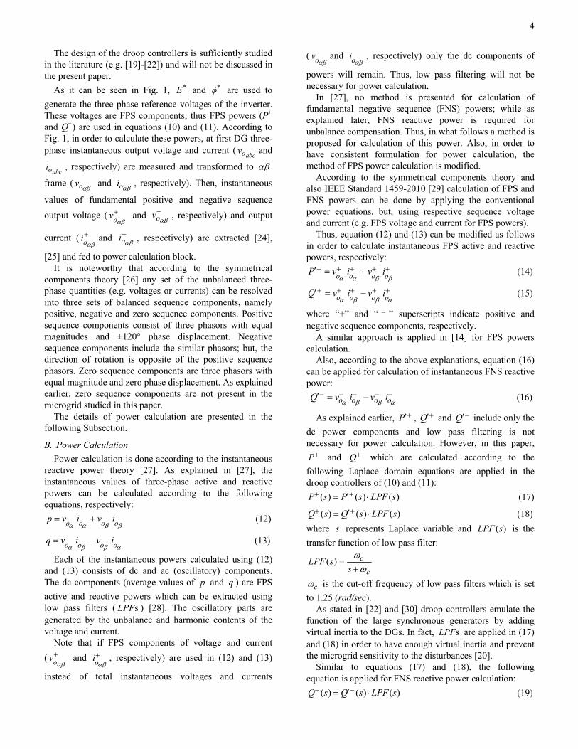
vR
αoi⊕
βoi
αVv
⊕
*Lvω
*Lvω−
vRβVv
Fig. 2. Virtual impedance block diagram.
Using LPF in (19) improves the stability of unbalance
compensation by preventing sudden change of Q− as a result of compensation.
As mentioned earlier, FPS powers are used by the power controllers to generate the reference values for the inverter output voltage phase and amplitude, respectively. FNS reactive power is applied for voltage unbalance compensation as explained in Subsection II-E.
It is noteworthy that in [14] _Q is calculated by multiplication of positive sequence voltage and negative sequence current. This calculation method doesn’t comply with the basic knowledge of symmetrical components [26] and also proposal of the IEEE Standard 1459-2010 [29].
C. Virtual Impedance Loop The accuracy of the power sharing provided by the droop
controllers is affected by the output impedance of the DG units as well as the line impedances. The virtual impedance is a fast control loop which is able to fix the phase and magnitude of the output impedance. Moreover, the effect of asymmetrical line impedances can be mitigated by proper design of the virtual impedance loop [19], [22], [30], [31].
Addition of the virtual resistance makes the oscillations of the system more damped [19]. The damping can also be provided by a physical resistance at the expense of efficiency decrease due to ohmic losses. In contrast with a physical resistance, the virtual resistance has no power losses, since is provided by a control loop; thus, it is possible to implement it without decreasing the efficiency [22].
Also, virtual inductance is considered to make the DG output impedance more inductive in order to improve the decoupling of P+ and Q+ . Thus, the virtual impedance enhances the droop controllers performance and stability [30], [32].
Furthermore, the virtual output impedance can provide additional features such as hot-swap operation and sharing of nonlinear load [19], [22]. These features fall out of the present paper scope.
As shown in Fig. 1, the instantaneous output current is fed to the virtual impedance control loop. Then, the output of this loop is subtracted from the voltage reference.
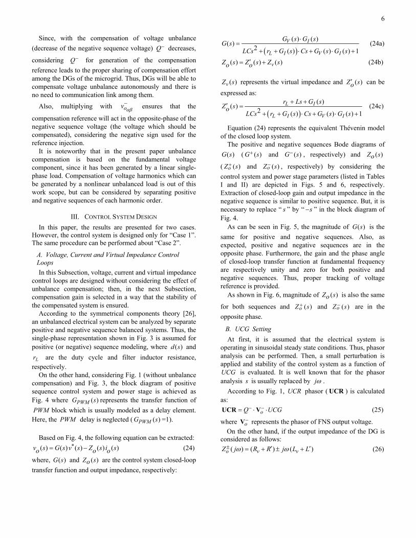
The virtual impedance is implemented as shown in Fig.2, where vR and vL are the virtual resistance and inductance values, respectively [32]. Thus, the following equations express the virtual impedance in αβ frame:
( )*V v o v oR i L ivα α β
ω= ⋅ − ⋅ ⋅ (20)
( )*V v o v oR i L ivβ β α
ω= ⋅ + ⋅ ⋅ (21)
D. Proportional-Resonant Voltage and Current Controllers Due to the difficulties of using proportional-integral (PI)
controllers to track non-dc variables, proportional-resonant (PR) controllers are usually preferred to control the voltage and current in stationary reference frame [33]. In this paper, PR voltage and current controllers are as (22) and (23):
( )22( )
*rV
V pVk s
G s ks ω
= ++
(22)
( )22( )
*rI
I pIk s
G s ks ω
= ++
(23)
where, pVk ( pIk ) and rVk ( rVk ) are the proportional and resonant coefficients of the voltage (current) controller, respectively.
As shown in Fig. 1, instantaneous filter inductor current ( αβLi ) is controlled by the current controller. By
controlling this current rather than the DG output current, influence of the load current on the control system performance is rejected, properly [34].
E. Voltage Unbalance Compensation It is well known that the voltage unbalance leads to
appearance of the negative sequence voltage. Thus, compensation of the voltage unbalance can be achieved through reducing negative sequence voltage.
As shown in Fig. 1, the output of “Unbalance Compensation” block (“UCR : Unbalance Compensation Reference”) is injected as a reference for the voltage controller. To generate this compensation reference, FNS reactive power ( Q− ) is multiplied by a constant (“UCG : Unbalance Compensation Gain”) and also by the
instantaneous FNS voltage ( −αβov ).
UCG is a constant which controls the compensation effort of DGs and should be selected in a way that the voltage unbalance is compensated to an acceptable level without making the control system unstable. The method of UCG setting is presented in Subsection III-B.
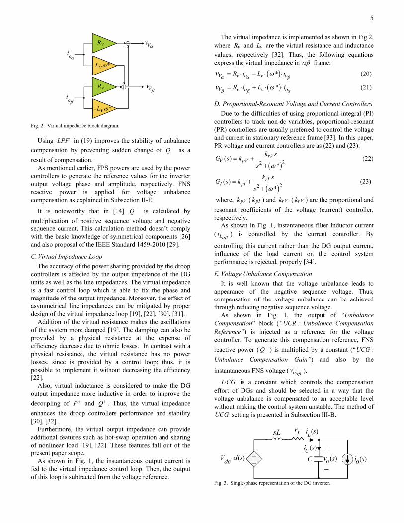
C+−
+
−( )soi( )sov
( )L si
( )V sdc d⋅( )C si
LrsL
Fig. 3. Single-phase representation of the DG inverter.
6
Since, with the compensation of voltage unbalance (decrease of the negative sequence voltage) Q− decreases,
considering Q− for generation of the compensation reference leads to the proper sharing of compensation effort among the DGs of the microgrid. Thus, DGs will be able to compensate voltage unbalance autonomously and there is no need to communication link among them.
Also, multiplying with −αβov ensures that the
compensation reference will act in the opposite-phase of the negative sequence voltage (the voltage which should be compensated), considering the negative sign used for the reference injection.
It is noteworthy that in the present paper unbalance compensation is based on the fundamental voltage component, since it has been generated by a linear single-phase load. Compensation of voltage harmonics which can be generated by a nonlinear unbalanced load is out of this work scope, but can be considered by separating positive and negative sequences of each harmonic order.
III. CONTROL SYSTEM DESIGN In this paper, the results are presented for two cases.
However, the control system is designed only for “Case 1”. The same procedure can be performed about “Case 2”.
A. Voltage, Current and Virtual Impedance Control Loops In this Subsection, voltage, current and virtual impedance
control loops are designed without considering the effect of unbalance compensation; then, in the next Subsection, compensation gain is selected in a way that the stability of the compensated system is ensured.
According to the symmetrical components theory [26], an unbalanced electrical system can be analyzed by separate positive and negative sequence balanced systems. Thus, the single-phase representation shown in Fig. 3 is assumed for positive (or negative) sequence modeling, where ( )d s and
Lr are the duty cycle and filter inductor resistance, respectively.
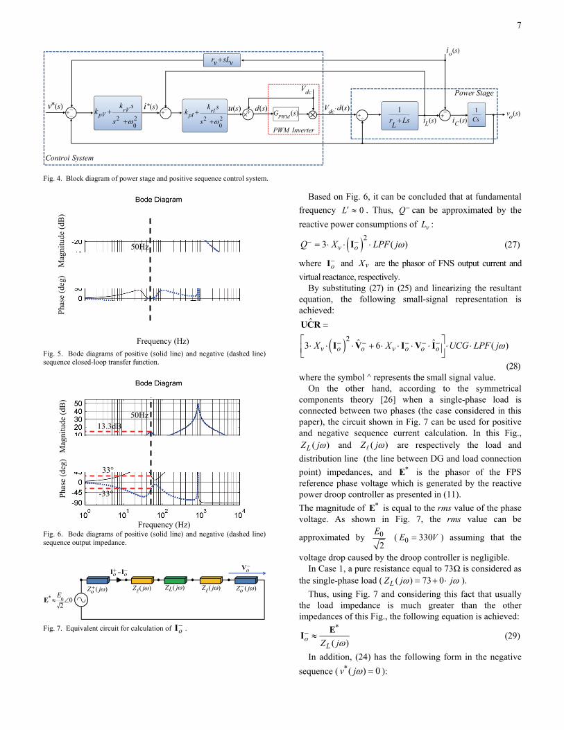
On the other hand, considering Fig. 1 (without unbalance compensation) and Fig. 3, the block diagram of positive sequence control system and power stage is achieved as Fig. 4 where ( )PWMG s represents the transfer function of PWM block which is usually modeled as a delay element. Here, the PWM delay is neglected ( ( )PWMG s =1).
Based on Fig. 4, the following equation can be extracted:
*( ) ( ) ( ) ( ) ( )v s G s v s Z s i so o o= − (24)
where, ( )G s and ( )Z so are the control system closed-loop transfer function and output impedance, respectively:
( )( ) ( )
( )2 ( ) ( ) ( ) 1
V I
L I V I
G s G sG s
LCs r G s Cs G s G s
⋅=
+ + ⋅ + ⋅ + (24a)
( ) ( ) ( )vZ s Z s Z so o′= + (24b)
( )vZ s represents the virtual impedance and ( )Z so′ can be
expressed as:
( )( )
( )2 ( ) ( ) ( ) 1
L I
L I V I
r Ls G sZ so
LCs r G s Cs G s G s
+ +′ =+ + ⋅ + ⋅ +
(24c)
Equation (24) represents the equivalent Thévenin model of the closed loop system.
The positive and negative sequences Bode diagrams of ( )G s ( ( )G s+ and ( )G s− , respectively) and ( )Z so
( ( )oZ s+ and ( )oZ s− , respectively) by considering the control system and power stage parameters (listed in Tables I and II) are depicted in Figs. 5 and 6, respectively. Extraction of closed-loop gain and output impedance in the negative sequence is similar to positive sequence. But, it is necessary to replace “ s ” by “ s− ” in the block diagram of Fig. 4.
As can be seen in Fig. 5, the magnitude of ( )G s is the same for positive and negative sequences. Also, as expected, positive and negative sequences are in the opposite phase. Furthermore, the gain and the phase angle of closed-loop transfer function at fundamental frequency are respectively unity and zero for both positive and negative sequences. Thus, proper tracking of voltage reference is provided.
As shown in Fig. 6, magnitude of ( )Z so is also the same
for both sequences and ( )oZ s+ and ( )oZ s− are in the
opposite phase.
B. UCG Setting At first, it is assumed that the electrical system is
operating in sinusoidal steady state conditions. Thus, phasor analysis can be performed. Then, a small perturbation is applied and stability of the control system as a function of UCG is evaluated. It is well known that for the phasor analysis s is usually replaced by jω .
According to Fig. 1, UCR phasor ( UCR ) is calculated as:
oQ UCG− −= ⋅ ⋅UCR V (25)
where o−V represents the phasor of FNS output voltage.
On the other hand, if the output impedance of the DG is considered as follows:
( ) ( ) ( )o v vZ j R R j L Lω ω± ′ ′= + ± + (26)
7
( )d s( )su*( )sv ( )dcV d s⋅
( )C si( )L si
*( )si+ −
− ( )PWMG s20
2 ω++
s
skk rV
pV20
2 ω++
s
skk rI
pI +
dcV
⊗ − LsLr +1
+
( )o sir sLv v+
− −Cs1 ( )v so
StagePower
SystemControl
+ ÷×
PWM Inverter
Fig. 4. Block diagram of power stage and positive sequence control system.
Fig. 5. Bode diagrams of positive (solid line) and negative (dashed line) sequence closed-loop transfer function.
Fig. 6. Bode diagrams of positive (solid line) and negative (dashed line) sequence output impedance.
( )oZ jω−( )LZ jω ( )Z jω
o−V
o o=+ −I I
( )Z jω0* 02
E≈ ∠E
( )oZ jω+
Fig. 7. Equivalent circuit for calculation of o
−I .
Based on Fig. 6, it can be concluded that at fundamental frequency 0≈′L . Thus, Q− can be approximated by the reactive power consumptions of vL :
( )23 ( )v oQ X LPF jω− −= ⋅ ⋅ ⋅I (27)
where o−I and vX are the phasor of FNS output current and
virtual reactance, respectively. By substituting (27) in (25) and linearizing the resultant
equation, the following small-signal representation is achieved:
( )2
ˆ
ˆ ˆ3 6 ( )v o o v o o oX X UCG LPF jω− − − − −
=
⎡ ⎤⋅ ⋅ ⋅ + ⋅ ⋅ ⋅ ⋅ ⋅ ⋅⎢ ⎥⎣ ⎦
UCR
I V I V I
(28) where the symbol ^ represents the small signal value.
On the other hand, according to the symmetrical components theory [26] when a single-phase load is connected between two phases (the case considered in this paper), the circuit shown in Fig. 7 can be used for positive and negative sequence current calculation. In this Fig.,
( )LZ jω and ( )Z jω are respectively the load and distribution line (the line between DG and load connection point) impedances, and *E is the phasor of the FPS reference phase voltage which is generated by the reactive power droop controller as presented in (11). The magnitude of *E is equal to the rms value of the phase voltage. As shown in Fig. 7, the rms value can be
approximated by 02
E ( 0 330E V= ) assuming that the
voltage drop caused by the droop controller is negligible. In Case 1, a pure resistance equal to 73Ω is considered as
the single-phase load ( ( ) 73 0LZ j jω ω= + ⋅ ). Thus, using Fig. 7 and considering this fact that usually
the load impedance is much greater than the other impedances of this Fig., the following equation is achieved:
*
( )oLZ jω
− ≈EI (29)
In addition, (24) has the following form in the negative sequence ( *( ) 0v jω = ):
Pha
se (d
eg)
Mag
nitu
de (d
B)
Frequency (Hz)
50Hz
50Hz 13.3dB
33°
-33°
Pha
se (d
eg)
Mag
nitu
de (d
B)
Frequency (Hz)
8
( )o o oZ jω− − −= − ⋅V I (30) Equation (30) can also be extracted according to Fig. 7.
Then, substituting (29) and (30) in (28) leads to the following equation:
( ) ( )2 2
2 2* *3 6 ( )ˆ ˆ ˆ( )
( ) ( )
( )
v v oo o
L L
X X Z j
Z j Z j
UCG LPF j
ω
ω ω
ω
−− −
⎡ ⎤⋅ ⋅ ⋅ ⋅ ⋅⎢ ⎥= − ⋅⎢ ⎥⎢ ⎥⎣ ⎦
⋅ ⋅
E ΕUCR V I
(31) Thus, when the unbalance compensation is activated, the
following small signal equation is achieved: ˆ ˆ( )o closed loop oG jω− −
−= ⋅V Ι (32)
being,
( )( )
( )
2*
22 *
2
22 *
( )
6 ( ) ( ) ( )
( ) 3 ( ) ( )
( ) ( )
( ) 3 ( ) ( )
closed loop
v o
vL
o L
vL
G j
G j X Z j UCG LPF j
Z j G j X UCG LPF j
Z j Z j
Z j G j X UCG LPF j
ω
ω ω ω
ω ω ω
ω ω
ω ω ω
−
− −
−
−
−
=
⋅ ⋅ ⋅ ⋅ ⋅ ⋅
+ ⋅ ⋅ ⋅ ⋅ ⋅
⋅−
+ ⋅ ⋅ ⋅ ⋅ ⋅
E
E
E
This equation is the negative sequence small signal form
of (24) by considering * ˆ( )v jω = −UCR (note to the negative sign used for injection of UCR in Fig. 1).
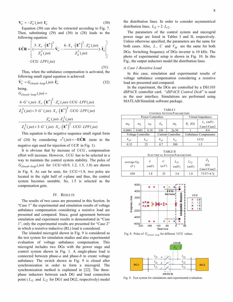
It is obvious that by increase of UCG , compensation effort will increase. However, UCG has to be selected in a way to maintain the control system stability. The poles of
( )closed loopG jω− for UCG =(0.9, 1.2, 1.5, 1.8) are shown
in Fig. 8. As can be seen, for UCG =1.8, two poles are located in the right half of s-plane and thus, the control system becomes unstable. So, 1.5 is selected as the compensation gain.
IV. RESULTS The results of two cases are presented in this Section. In
“Case 1” the experimental and simulation results of voltage unbalance compensation considering a resistive load are presented and compared. Since, good agreement between simulation and experiment results is demonstrated in “Case 1”, only the experimental results are presented for “Case 2” in which a resistive-inductive (RL) load is considered.
The islanded microgrid shown in Fig. 9 is considered as the test system for simulation studies and also experimental evaluation of voltage unbalance compensation. This microgrid includes two DGs with the power stage and control system shown in Fig. 1. A single-phase load is connected between phase-a and phase-b to create voltage unbalance. The switch shown in Fig. 9 is closed after synchronization in order to form a microgrid. The synchronization method is explained in [22]. The three-phase inductors between each DG and load connection point ( 1L and 2L for DG1 and DG2, respectively) model
the distribution lines. In order to consider asymmetrical distribution lines, 1 22L L= ⋅ .
The parameters of the control system and microgrid power stage are listed in Tables I and II, respectively. Unless otherwise specified, the parameters are the same for both cases. Also, L , C and dcV are the same for both DGs. Switching frequency of DGs inverter is 10 kHz. The photo of experimental setup is shown in Fig. 10. In this Fig., the output inductors model the distribution lines.
A. Case 1-Resistive Load In this case, simulation and experimental results of
voltage unbalance compensation considering a resistive load are presented and compared.
In the experiment, the DGs are controlled by a DS1103 dSPACE controller card. “dSPACE Control Desk” is used as the user interface. Simulations are performed using MATLAB/Simulink software package.
TABLE I
CONTROL SYSTEM PARAMETERS Power Controllers Virtual Impedance
Pm Im Pn 0E 0ω vR ( )Ω vL ( )mH Case1/Case2
0.0001 0.001 0.18 330 2π.50 1 8/4 Voltage Controller Current Controller Unbalance Compensator
pVk rVk pIk rIk UCG
0.35 25 0.7 500 1.5
TABLE II ELECTRICAL SYSTEM PARAMETERS
average dcV ( )V
L ( )mH
C ( )Fμ
1L
( )mH 2L
( )mH
LZ ( )Ω
Case1/Case2650 1.8 25 3.6 1.8 73/57+4.7j
Fig. 8. Poles of loopclosedG − for different UCG
values.
1L
DG2DG1
a
b
c
LOAD
SWITCH
1L
1L
2L
2L2L
LZ
Fig. 9. Test system for simulations and experimental evaluation.
UnstableRe
gion
UCG increase
9
Inverters
Voltage Sensors
Filter Capacitors
I/O Box
dSpace Control Desk
Current Sensors
1103 dSpace
SwitchOutput Inductors
Filter Inductors
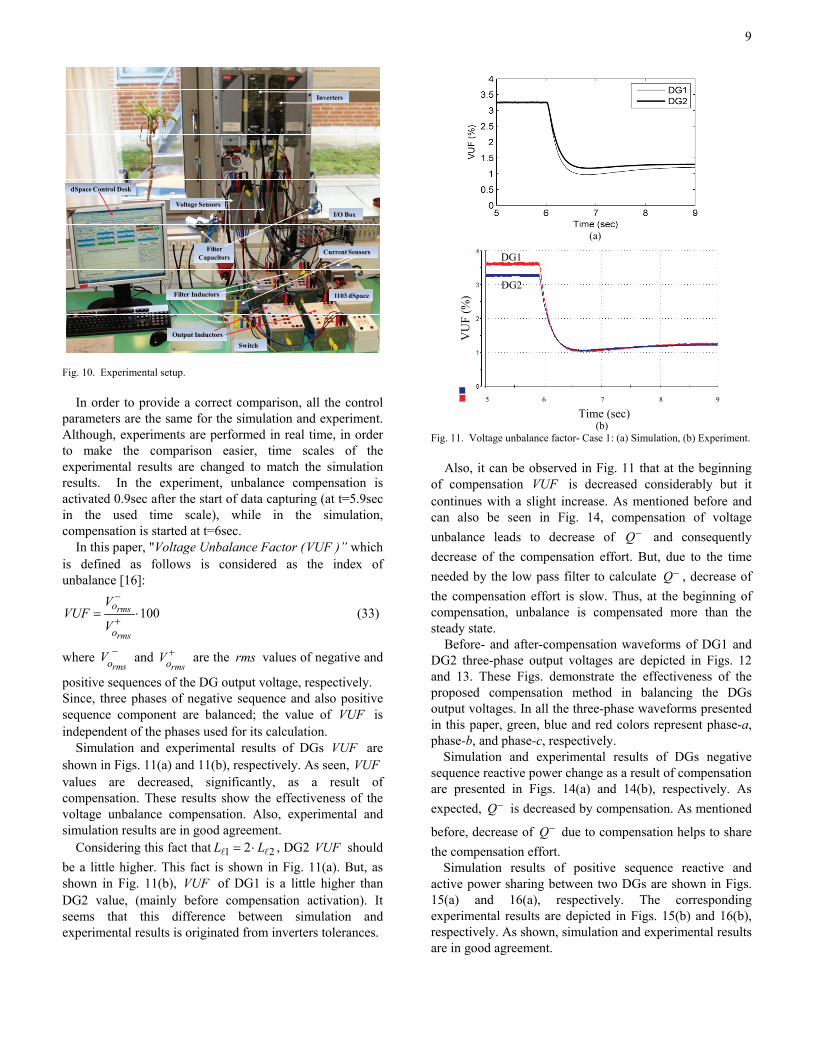
Fig. 10. Experimental setup.
In order to provide a correct comparison, all the control parameters are the same for the simulation and experiment. Although, experiments are performed in real time, in order to make the comparison easier, time scales of the experimental results are changed to match the simulation results. In the experiment, unbalance compensation is activated 0.9sec after the start of data capturing (at t=5.9sec in the used time scale), while in the simulation, compensation is started at t=6sec.
In this paper, "Voltage Unbalance Factor (VUF )” which is defined as follows is considered as the index of unbalance [16]:
100rms
rms
o
o
VVUF
V
−
+= ⋅ (33)
where rmsoV −
and
rmsoV +
are the rms values of negative and
positive sequences of the DG output voltage, respectively. Since, three phases of negative sequence and also positive sequence component are balanced; the value of VUF is independent of the phases used for its calculation.
Simulation and experimental results of DGs VUF are shown in Figs. 11(a) and 11(b), respectively. As seen, VUF values are decreased, significantly, as a result of compensation. These results show the effectiveness of the voltage unbalance compensation. Also, experimental and simulation results are in good agreement.
Considering this fact that 1 22L L= ⋅ , DG2 VUF should be a little higher. This fact is shown in Fig. 11(a). But, as shown in Fig. 11(b), VUF of DG1 is a little higher than DG2 value, (mainly before compensation activation). It seems that this difference between simulation and experimental results is originated from inverters tolerances.
(a)
(b) Fig. 11. Voltage unbalance factor- Case 1: (a) Simulation, (b) Experiment.
Also, it can be observed in Fig. 11 that at the beginning
of compensation VUF is decreased considerably but it continues with a slight increase. As mentioned before and can also be seen in Fig. 14, compensation of voltage unbalance leads to decrease of Q− and consequently decrease of the compensation effort. But, due to the time needed by the low pass filter to calculate Q− , decrease of the compensation effort is slow. Thus, at the beginning of compensation, unbalance is compensated more than the steady state.
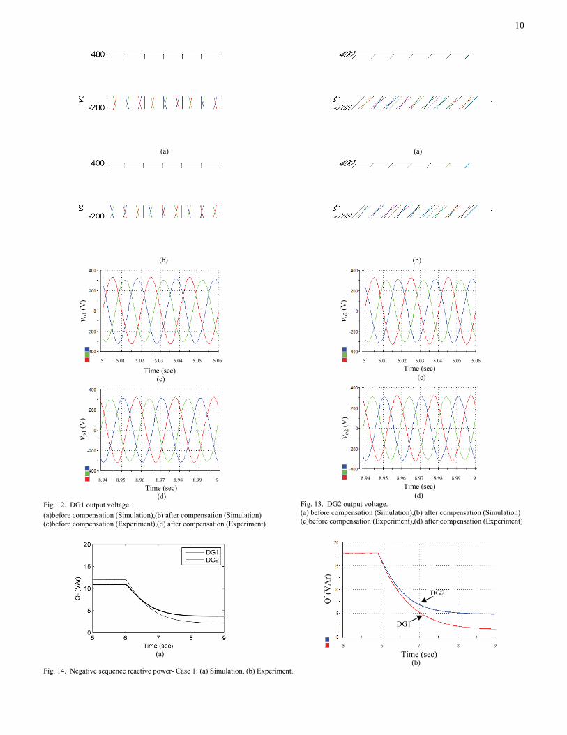
Before- and after-compensation waveforms of DG1 and DG2 three-phase output voltages are depicted in Figs. 12 and 13. These Figs. demonstrate the effectiveness of the proposed compensation method in balancing the DGs output voltages. In all the three-phase waveforms presented in this paper, green, blue and red colors represent phase-a, phase-b, and phase-c, respectively.
Simulation and experimental results of DGs negative sequence reactive power change as a result of compensation are presented in Figs. 14(a) and 14(b), respectively. As expected, Q− is decreased by compensation. As mentioned
before, decrease of Q− due to compensation helps to share the compensation effort.
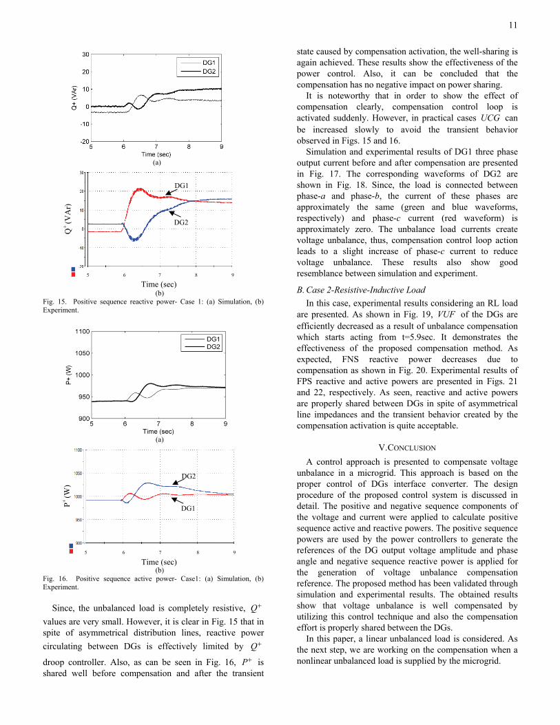
Simulation results of positive sequence reactive and active power sharing between two DGs are shown in Figs. 15(a) and 16(a), respectively. The corresponding experimental results are depicted in Figs. 15(b) and 16(b), respectively. As shown, simulation and experimental results are in good agreement.
5 6 7 8 9
VU
F (%
)
Time (sec)
DG1
DG2
10
(a)
(b)
(c)
(d) Fig. 12. DG1 output voltage. (a)before compensation (Simulation),(b) after compensation (Simulation) (c)before compensation (Experiment),(d) after compensation (Experiment)
(a)
(b)
(c)
(d) Fig. 13. DG2 output voltage. (a) before compensation (Simulation),(b) after compensation (Simulation) (c)before compensation (Experiment),(d) after compensation (Experiment)
(a)
(b) Fig. 14. Negative sequence reactive power- Case 1: (a) Simulation, (b) Experiment.
v o1 (
V)
Time (sec) 5 5.01 5.02 5.03 5.04 5.05 5.06
8.94 8.95 8.96 8.97 8.98 8.99 9
v o2 (
V)
Time (sec)
5 6 7 8 9
Q- (V
Ar)
Time (sec)
DG1
DG2
8.94 8.95 8.96 8.97 8.98 8.99 9
v o1 (
V)
Time (sec)
5 5.01 5.02 5.03 5.04 5.05 5.06
v o2 (
V)
Time (sec)
11
(a)
(b) Fig. 15. Positive sequence reactive power- Case 1: (a) Simulation, (b) Experiment.
(a)
(b) Fig. 16. Positive sequence active power- Case1: (a) Simulation, (b) Experiment.
Since, the unbalanced load is completely resistive, Q+ values are very small. However, it is clear in Fig. 15 that in spite of asymmetrical distribution lines, reactive power circulating between DGs is effectively limited by Q+
droop controller. Also, as can be seen in Fig. 16, P+ is shared well before compensation and after the transient
state caused by compensation activation, the well-sharing is again achieved. These results show the effectiveness of the power control. Also, it can be concluded that the compensation has no negative impact on power sharing.
It is noteworthy that in order to show the effect of compensation clearly, compensation control loop is activated suddenly. However, in practical cases UCG can be increased slowly to avoid the transient behavior observed in Figs. 15 and 16.
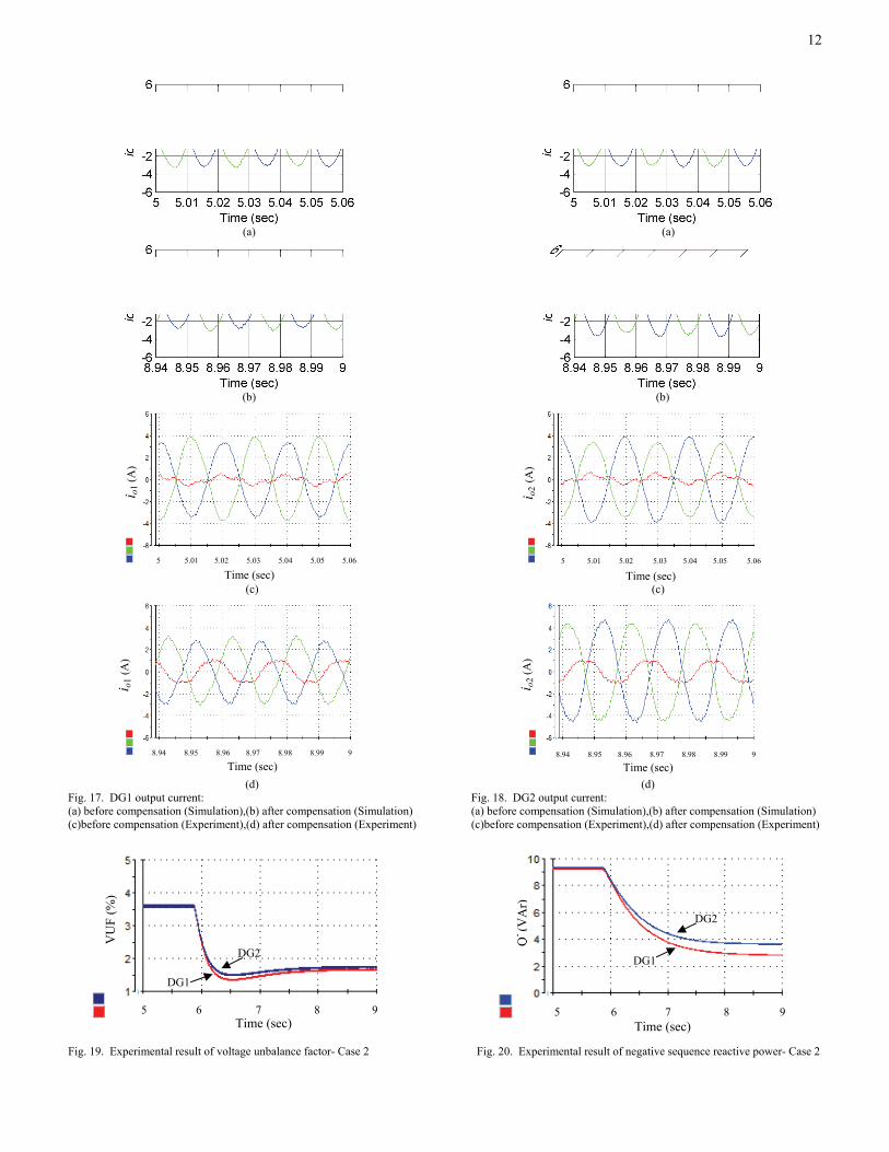
Simulation and experimental results of DG1 three phase output current before and after compensation are presented in Fig. 17. The corresponding waveforms of DG2 are shown in Fig. 18. Since, the load is connected between phase-a and phase-b, the current of these phases are approximately the same (green and blue waveforms, respectively) and phase-c current (red waveform) is approximately zero. The unbalance load currents create voltage unbalance, thus, compensation control loop action leads to a slight increase of phase-c current to reduce voltage unbalance. These results also show good resemblance between simulation and experiment.
B. Case 2-Resistive-Inductive Load In this case, experimental results considering an RL load
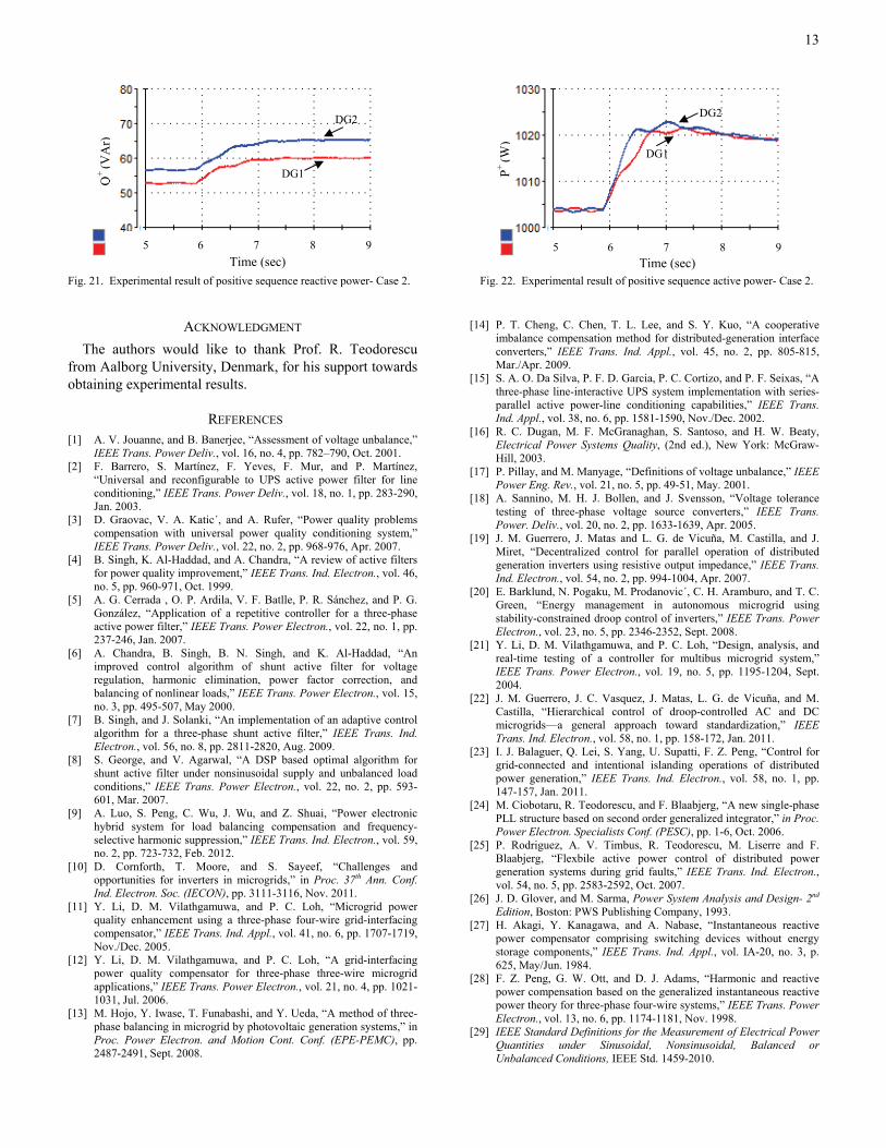
are presented. As shown in Fig. 19, VUF of the DGs are efficiently decreased as a result of unbalance compensation which starts acting from t=5.9sec. It demonstrates the effectiveness of the proposed compensation method. As expected, FNS reactive power decreases due to compensation as shown in Fig. 20. Experimental results of FPS reactive and active powers are presented in Figs. 21 and 22, respectively. As seen, reactive and active powers are properly shared between DGs in spite of asymmetrical line impedances and the transient behavior created by the compensation activation is quite acceptable.
V. CONCLUSION A control approach is presented to compensate voltage
unbalance in a microgrid. This approach is based on the proper control of DGs interface converter. The design procedure of the proposed control system is discussed in detail. The positive and negative sequence components of the voltage and current were applied to calculate positive sequence active and reactive powers. The positive sequence powers are used by the power controllers to generate the references of the DG output voltage amplitude and phase angle and negative sequence reactive power is applied for the generation of voltage unbalance compensation reference. The proposed method has been validated through simulation and experimental results. The obtained results show that voltage unbalance is well compensated by utilizing this control technique and also the compensation effort is properly shared between the DGs.
In this paper, a linear unbalanced load is considered. As the next step, we are working on the compensation when a nonlinear unbalanced load is supplied by the microgrid.
5 6 7 8 9
Q+
(VA
r)
Time (sec)
DG2
DG1
P+ (W
)
Time (sec)
DG1
DG2
5 6 7 8 9
12
(a)
(b)
(c)
(d) Fig. 17. DG1 output current: (a) before compensation (Simulation),(b) after compensation (Simulation) (c)before compensation (Experiment),(d) after compensation (Experiment)
(a)
(b)
(c)
(d) Fig. 18. DG2 output current: (a) before compensation (Simulation),(b) after compensation (Simulation) (c)before compensation (Experiment),(d) after compensation (Experiment)
Fig. 19. Experimental result of voltage unbalance factor- Case 2 Fig. 20. Experimental result of negative sequence reactive power- Case 2
5 6 7 8 9
Q- (V
Ar)
Time (sec)
DG1
DG2
5 6 7 8 9
VU
F (%
)
Time (sec)
DG1
DG2
8.94 8.95 8.96 8.97 8.98 8.99 9
i o1 (A
)
Time (sec) 8.94 8.95 8.96 8.97 8.98 8.99 9
i o2 (A
)
Time (sec)
5 5.01 5.02 5.03 5.04 5.05 5.06
i o1 (A
)
Time (sec) 5 5.01 5.02 5.03 5.04 5.05 5.06
i o2 (A
)
Time (sec)
13
Fig. 21. Experimental result of positive sequence reactive power- Case 2. Fig. 22. Experimental result of positive sequence active power- Case 2.
ACKNOWLEDGMENT The authors would like to thank Prof. R. Teodorescu
from Aalborg University, Denmark, for his support towards obtaining experimental results.
REFERENCES [1] A. V. Jouanne, and B. Banerjee, “Assessment of voltage unbalance,”
IEEE Trans. Power Deliv., vol. 16, no. 4, pp. 782–790, Oct. 2001. [2] F. Barrero, S. Martínez, F. Yeves, F. Mur, and P. Martínez,
“Universal and reconfigurable to UPS active power filter for line conditioning,” IEEE Trans. Power Deliv., vol. 18, no. 1, pp. 283-290, Jan. 2003.
[3] D. Graovac, V. A. Katic´, and A. Rufer, “Power quality problems compensation with universal power quality conditioning system,” IEEE Trans. Power Deliv., vol. 22, no. 2, pp. 968-976, Apr. 2007.
[4] B. Singh, K. Al-Haddad, and A. Chandra, “A review of active filters for power quality improvement,” IEEE Trans. Ind. Electron., vol. 46, no. 5, pp. 960-971, Oct. 1999.
[5] A. G. Cerrada , O. P. Ardila, V. F. Batlle, P. R. Sánchez, and P. G. González, “Application of a repetitive controller for a three-phase active power filter,” IEEE Trans. Power Electron., vol. 22, no. 1, pp. 237-246, Jan. 2007.
[6] A. Chandra, B. Singh, B. N. Singh, and K. Al-Haddad, “An improved control algorithm of shunt active filter for voltage regulation, harmonic elimination, power factor correction, and balancing of nonlinear loads,” IEEE Trans. Power Electron., vol. 15, no. 3, pp. 495-507, May 2000.
[7] B. Singh, and J. Solanki, “An implementation of an adaptive control algorithm for a three-phase shunt active filter,” IEEE Trans. Ind. Electron., vol. 56, no. 8, pp. 2811-2820, Aug. 2009.
[8] S. George, and V. Agarwal, “A DSP based optimal algorithm for shunt active filter under nonsinusoidal supply and unbalanced load conditions,” IEEE Trans. Power Electron., vol. 22, no. 2, pp. 593-601, Mar. 2007.
[9] A. Luo, S. Peng, C. Wu, J. Wu, and Z. Shuai, “Power electronic hybrid system for load balancing compensation and frequency-selective harmonic suppression,” IEEE Trans. Ind. Electron., vol. 59, no. 2, pp. 723-732, Feb. 2012.
[10] D. Cornforth, T. Moore, and S. Sayeef, “Challenges and opportunities for inverters in microgrids,” in Proc. 37th Ann. Conf. Ind. Electron. Soc. (IECON), pp. 3111-3116, Nov. 2011.
[11] Y. Li, D. M. Vilathgamuwa, and P. C. Loh, “Microgrid power quality enhancement using a three-phase four-wire grid-interfacing compensator,” IEEE Trans. Ind. Appl., vol. 41, no. 6, pp. 1707-1719, Nov./Dec. 2005.
[12] Y. Li, D. M. Vilathgamuwa, and P. C. Loh, “A grid-interfacing power quality compensator for three-phase three-wire microgrid applications,” IEEE Trans. Power Electron., vol. 21, no. 4, pp. 1021-1031, Jul. 2006.
[13] M. Hojo, Y. Iwase, T. Funabashi, and Y. Ueda, “A method of three-phase balancing in microgrid by photovoltaic generation systems,” in Proc. Power Electron. and Motion Cont. Conf. (EPE-PEMC), pp. 2487-2491, Sept. 2008.
[14] P. T. Cheng, C. Chen, T. L. Lee, and S. Y. Kuo, “A cooperative imbalance compensation method for distributed-generation interface converters,” IEEE Trans. Ind. Appl., vol. 45, no. 2, pp. 805-815, Mar./Apr. 2009.
[15] S. A. O. Da Silva, P. F. D. Garcia, P. C. Cortizo, and P. F. Seixas, “A three-phase line-interactive UPS system implementation with series-parallel active power-line conditioning capabilities,” IEEE Trans. Ind. Appl., vol. 38, no. 6, pp. 1581-1590, Nov./Dec. 2002.
[16] R. C. Dugan, M. F. McGranaghan, S. Santoso, and H. W. Beaty, Electrical Power Systems Quality, (2nd ed.), New York: McGraw-Hill, 2003.
[17] P. Pillay, and M. Manyage, “Definitions of voltage unbalance,” IEEE Power Eng. Rev., vol. 21, no. 5, pp. 49-51, May. 2001.
[18] A. Sannino, M. H. J. Bollen, and J. Svensson, “Voltage tolerance testing of three-phase voltage source converters,” IEEE Trans. Power. Deliv., vol. 20, no. 2, pp. 1633-1639, Apr. 2005.
[19] J. M. Guerrero, J. Matas and L. G. de Vicuña, M. Castilla, and J. Miret, “Decentralized control for parallel operation of distributed generation inverters using resistive output impedance,” IEEE Trans. Ind. Electron., vol. 54, no. 2, pp. 994-1004, Apr. 2007.
[20] E. Barklund, N. Pogaku, M. Prodanovic´, C. H. Aramburo, and T. C. Green, “Energy management in autonomous microgrid using stability-constrained droop control of inverters,” IEEE Trans. Power Electron., vol. 23, no. 5, pp. 2346-2352, Sept. 2008.
[21] Y. Li, D. M. Vilathgamuwa, and P. C. Loh, “Design, analysis, and real-time testing of a controller for multibus microgrid system,” IEEE Trans. Power Electron., vol. 19, no. 5, pp. 1195-1204, Sept. 2004.
[22] J. M. Guerrero, J. C. Vasquez, J. Matas, L. G. de Vicuña, and M. Castilla, “Hierarchical control of droop-controlled AC and DC microgrids—a general approach toward standardization,” IEEE Trans. Ind. Electron., vol. 58, no. 1, pp. 158-172, Jan. 2011.
[23] I. J. Balaguer, Q. Lei, S. Yang, U. Supatti, F. Z. Peng, “Control for grid-connected and intentional islanding operations of distributed power generation,” IEEE Trans. Ind. Electron., vol. 58, no. 1, pp. 147-157, Jan. 2011.
[24] M. Ciobotaru, R. Teodorescu, and F. Blaabjerg, “A new single-phase PLL structure based on second order generalized integrator,” in Proc. Power Electron. Specialists Conf. (PESC), pp. 1-6, Oct. 2006.
[25] P. Rodriguez, A. V. Timbus, R. Teodorescu, M. Liserre and F. Blaabjerg, “Flexbile active power control of distributed power generation systems during grid faults,” IEEE Trans. Ind. Electron., vol. 54, no. 5, pp. 2583-2592, Oct. 2007.
[26] J. D. Glover, and M. Sarma, Power System Analysis and Design- 2nd Edition, Boston: PWS Publishing Company, 1993.
[27] H. Akagi, Y. Kanagawa, and A. Nabase, “Instantaneous reactive power compensator comprising switching devices without energy storage components,” IEEE Trans. Ind. Appl., vol. IA-20, no. 3, p. 625, May/Jun. 1984.
[28] F. Z. Peng, G. W. Ott, and D. J. Adams, “Harmonic and reactive power compensation based on the generalized instantaneous reactive power theory for three-phase four-wire systems,” IEEE Trans. Power Electron., vol. 13, no. 6, pp. 1174-1181, Nov. 1998.
[29] IEEE Standard Definitions for the Measurement of Electrical Power Quantities under Sinusoidal, Nonsinusoidal, Balanced or Unbalanced Conditions, IEEE Std. 1459-2010.
5 6 7 8 9
Q+
(VA
r)
Time (sec)
DG1
DG2
5 6 7 8 9
P+ (W
)
Time (sec)
DG1
DG2
14
[30] J. M. Guerrero, L. G. Vicuña, J. Matas, M. Castilla, and J. Miret, “Output impedance design of parallel-connected UPS inverters with wireless load sharing control,” IEEE Trans. Ind. Electron., vol. 52, no. 4, pp. 1126-1135, Aug. 2005.
[31] J. M. Guerrero, J. Matas and L. G. de Vicuña, M. Castilla, and J. Miret, “Wireless-control strategy for parallel operation of distributed-generation inverters,” IEEE Trans. Ind. Electron., vol. 53, no. 5, pp. 1461-1470, Oct. 2006.
[32] J. He, and Y. W. Li “Analysis and design of interfacing inverter output virtual impedance in a low voltage microgrid,” in Proc. Energy Conv. Cong. and Exp. (ECCE), pp. 2857–2864, Sept. 2010.
[33] F. Blaabjerg, R. Teodorescu, M. Liserre and A. V. Timbus, “Overview of control and grid synchronization for distributed power generation systems,” IEEE Trans. Ind. Electron., vol. 53, no. 5, pp. 1398-1409, Oct. 2006.
[34] P. C. Loh, and D. G. Holmes, “Analysis of multiloop control strategies for LC/CL/LCL-filtered voltage-source and current-source inverters,” IEEE Trans. Ind. Appl., vol. 41, no. 2, pp. 644-654, Mar./Apr. 2005.
Mehdi Savaghebi (S’06) was born in Karaj, Iran, in 1983. He received the B.S. degree from Tehran University, Iran, in 2004 and the M.S. degree with highest honors from Iran University of Science and Technology (IUST), in 2006, both in electrical engineering. He is now perusing the Ph.D. degree in IUST.
His main research interests include Distributed Generation systems, Microgrids and power quality issues of electrical systems.
Alireza Jalilian was born in Yazd, Iran, in 1961. He received the B.S. degree in electrical engineering from Mazandaran University, Babol, Iran, in 1989, and the M.S. and Ph.D. degrees from the University of Wollongong, Wollongong, New South Wales, Australia, in 1992 and 1997, respectively.
He joined the Power Group of the Department of Electrical Engineering at the Iran University of Science and Technology in 1998, where he is an
Assistant Professor. His research interests are power-quality problems causes and effects as well as mitigation methods.
Juan C. Vasquez received the B.S. degree in Electronics Engineering from Autonoma University of Manizales, Colombia, in 2004 where he has been teaching courses on digital circuits, servo systems and flexible manufacturing systems. In 2009, he has received his Ph.D. degree from the Technical University of Catalonia, Barcelona, Spain in 2009 at the Department of Automatic Control Systems and Computer Engineering, from Technical University of Catalonia, Barcelona
Spain, where he worked as a Post-doc Assistant and also taught courses based on renewable energy systems. Currently, he is an Assistant Professor in Aalborg University, Denmark. His research interests include modeling, simulation, and power management applied to the Distributed Generation in Microgrids.
Josep M. Guerrero (S’01–M’03–SM’08) was born in Barcelona, Spain, in 1973. He received the B.S. degree in telecommunications engineering, the M.S. degree in electronics engineering, and the Ph.D. degree in power electronics from the Technical University of Catalonia, Barcelona, Spain, in 1997, 2000 and 2003, respectively.
He is an Associate Professor with the Department of Automatic Control Systems and
Computer Engineering, Technical University of Catalonia, Barcelona, where he currently teaches courses on digital signal processing, FPGAs, microprocessors, and renewable energy. Since 2004, he has been responsible for the Renewable Energy Laboratory, Escola Industrial de Barcelona. He has been a visiting Professor at Zhejiang University, China, and University of Cergy-Pontoise, France. From 2011, he is a Full Professor at the Department of Energy Technology, Aalborg University, Denmark, where he is the responsible of the Microgrids research program. His research interests is oriented to different Microgrids aspects, including power electronics, distributed energy storage systems, hierarchical and cooperative control, energy management systems and optimization of microgrids and islanded minigrids.
Dr. Guerrero is an Associate Editor for the IEEE Transactions on Power Electronics, IEEE Transactions on Industrial Electronics, and IEEE Industrial Electronics Magazine. He has been Guest Editor of the IEEE Transactions on Power Electronics Special Issues: Power Electrics for Wind Energy Conversion and Power Electronics for Microgrids; and the IEEE Transactions on Industrial Electronics Special Sections: Uninterruptible Power Supplies (UPS) systems, Renewable Energy Systems, Distributed Generation and Microgrids, and Industrial Applications and Implementation Issues of the Kalman Filter He currently chairs the Renewable Energy Systems Technical Committee of IEEE IES.