aalborg universitet mission-profile-based lifetime ... · [email protected],...
TRANSCRIPT

Aalborg Universitet
Mission-Profile-Based Lifetime Prediction for a SiC mosfet Power Module Using aMulti-Step Condition-Mapping Simulation Strategy
Ceccarelli, Lorenzo; Kotecha, Ramchandra M.; Bahman, Amir Sajjad; Iannuzzo, Francesco;Mantooth, Homer AlanPublished in:IEEE Transactions on Power Electronics
DOI (link to publication from Publisher):10.1109/TPEL.2019.2893636
Publication date:2019
Document VersionAccepted author manuscript, peer reviewed version
Link to publication from Aalborg University
Citation for published version (APA):Ceccarelli, L., Kotecha, R. M., Bahman, A. S., Iannuzzo, F., & Mantooth, H. A. (2019). Mission-Profile-BasedLifetime Prediction for a SiC mosfet Power Module Using a Multi-Step Condition-Mapping Simulation Strategy.IEEE Transactions on Power Electronics, 34(10), 9698-9708. [8616890].https://doi.org/10.1109/TPEL.2019.2893636
General rightsCopyright and moral rights for the publications made accessible in the public portal are retained by the authors and/or other copyright ownersand it is a condition of accessing publications that users recognise and abide by the legal requirements associated with these rights.
? Users may download and print one copy of any publication from the public portal for the purpose of private study or research. ? You may not further distribute the material or use it for any profit-making activity or commercial gain ? You may freely distribute the URL identifying the publication in the public portal ?
Take down policyIf you believe that this document breaches copyright please contact us at [email protected] providing details, and we will remove access tothe work immediately and investigate your claim.

Mission-Profile-Based Lifetime Prediction for a SiC MOSFET Power Module using a Multi-Step
Condition-Mapping Simulation Strategy Lorenzo Ceccarellia, Ramchandra Kotechab, Student Members, IEEE, Amir Sajjad Bahmana, Member, IEEE,
Francesco Iannuzzoa, Senior Member, IEEE, H. Alan Mantoothb, Fellow, IEEE
a Department of Energy Technology, Aalborg University, Pontoppidanstraede 111, 9220 Aalborg East, Denmark [email protected], [email protected], [email protected]
b Electrical Engineering, University of Arkansas, Fayetteville, AR 72701, U.S.A [email protected], [email protected]
Abstract- The reliability analysis and lifetime prediction for SiC-based power modules is crucial in order to fulfill the design specifications for next-generation power converters. This paper presents a fast mission-profile-based simulation strategy for a commercial 1.2 kV all-SiC power module used in a photovoltaic (PV) inverter topology. The approach relies on a fast condition-mapping simulation structure and the detailed electro-thermal modeling of the module topology and devices. Both parasitic electrical elements and thermal impedance network are extracted from the finite-element analysis of the module geometry. The use of operating conditions mapping and look-up tables enables the simulation of very long timescales in only a few minutes, preserving at the same time the accuracy of circuit-based simulations. The accumulated damage related to thermo-mechanical stress on the module is determined analytically and a simple consumed lifetime calculation is performed for two different mission profiles and compared in different operating conditions.
I. INTRODUCTION
Silicon Carbide (SiC) power devices and modules are
increasingly emerging in the design of power electronic converters [1, 2]. This is mainly due to their promising high temperature and high frequency operative capability [3]. SiC modules find advantage in those applications where high efficiency, more integration and higher power density are prioritized, and can pay off the higher cost of such devices [4]. The SiC MOSFET is now an established device in terms of manufacturing and many off-the-shelf products are available, rated up to 1.7 kV and 500 A [5]. Nevertheless, despite their inherent advantages, fulfilling the converter design specifications is still a challenge for many applications, with increasing demand for reliability and cost constraints. Higher current density capability,
together with higher thermal conductivity, determines higher temperature variations in SiC devices in comparison to Si devices rated at the same power. Therefore, the lifetime prediction of SiC devices becomes a critical issue in the design of emerging power electronic converters.
Substantial efforts have been invested in the reliability prediction of grid-connected converters, especially for photovoltaic (PV) and wind energy generation [6–8], an emerging field for SiC devices. Most of the component-level reliability prediction methods are based on the Military-Handbook-217F [9]. The methods in such handbooks are easy-to-use, but may not be suitable for the design of components in real field operation, since they are based on constant failure rates and components wear-out is neglected. In addition, on the FIDES guide [10], accelerated factors for different stressors, e.g. temperature and humidity, have been provided, also including several wear out failure mechanisms. By the way, the data provided in FIDES are limited to a few components, e.g. IGBTs and capacitors, but without making a difference between different technologies and manufacturers. Thus, a more specific component-level reliability analysis and the impact of real field mission profiles have to be considered. A very thorough and innovative multi-timescale stress modeling approach has been presented at Aalborg University in 2015 by Ma et al. in [11, 12], introducing the possibility to step through different time constants (electrical, thermal and mechanical) for the analysis of power converter loading profiles. Several other studies, e.g. [13–17], have studied mission-profile-based approaches for Si IGBT modules. Still, a limited amount of research works [18]–[20] have applied it to SiC devices using accurate electro-thermal and device modeling.
In addition, the challenge in lifetime prediction is to identify the failure and degradation mechanisms and their modeling [21, 22]. The main long-term failure mechanisms of power semiconductor modules is the bond

wire and solder fatigue due to temperature-induced mechanical stress. The degradation process has been extensively studied in the case of Si IGBT modules and several lifetime modeling techniques have been introduced, both physical [23] and empirical [24]. Nowadays, the wire bonding packaging technology for commercial SiC MOSFET power modules is, in fact, identical to the one widely used for Si IGBT modules. Therefore, the same degradation and failure mechanisms have been observed in [25], and bond wire damage, together with die-attach degradation, are still the predominant cause of thermal-related failure and aging. Nevertheless, the device and material physical characteristics – especially thermal properties - are significantly different. SiC technology relies on smaller and power-dense chips, which can undergo a considerably heavier thermal stress. Therefore, new physics-based models are needed for both device and power module, in order to properly estimate their reliability.
This paper’s structure is the following: Section II explains the challenges related to the mission-profile-based lifetime prediction and Section III presents the proposed modeling and simulation approach. In Section IV the strategy is applied to a three phase grid-connected PV inverter chosen as a case study. The results and validity of this methodology are discussed in Section V and final remarks are provided in Section VI.
II. MISSION-PROFILE-BASED LIFETIME PREDICTION
STRATEGY
The lifetime prediction of a power module requires a comprehensive set of elements: 1) a semiconductor device model that can accurately estimate the power loss in a wide range of operating conditions, including high temperature; 2) the electrical model has to describe properly the packaging-related parasitic elements, which can significantly influence the overall power loss; 3) a
thermal model capable of estimating the temperature stress throughout the module’s lifetime; 4) a reliability lifetime model describing one or more physical failure or degradation mechanisms taking place inside the module; 5) a damage accumulation method to calculate the consumed lifetime and the degradation of the device parameters. Advanced multi-physics simulation tools based on Finite Element Analysis (FEA) offer outstanding accuracy, but their huge computational cost would make it impractical to simulate millions of switching events. On the contrary, compact electro-thermal circuit models can be very fast, with a small percentage loss in accuracy. All these elements have to be specifically tuned on the particular case study and necessary approximations and assumptions have to be worked out to speed up the simulation process without losing accuracy.
Fig. 1. A general mission-profile-based electrothermal simulation workflow.
Fig. 2. Proposed mission-profile-based electrothermal simulation strategy.

A. Mission-Profile-Based Simulation Challenges
During the normal operating lifetime of a converter, a power device may experience deep changes in its working conditions, depending on the load cycle (mission profile) required for the specific application, and the external conditions, i.e. ambient temperature variations. Fig. 1 depicts the general workflow for mission-profile-based electrothermal simulation aimed to reliability analysis [11]. The design of a converter topology with determined specifications and the selection of a device or module capable of handling the required load cycle, working within the safe-operating area (SOA), is driven by a mission profile study. A converter model with a defined switching pattern is selected and thus the mission profile can be translated into the equivalent device loading, as presented in [17]. Many examples of electrothermal device simulation using compact or behavioral models are available in literature [26–29]. The typical approach is the use of compact or behavioral electrical device models in conjunction with a heatsink thermal model. The obtained thermal stress is thus translated in lifetime consumption by means of a lifetime model [11]. The major obstacle for such methods is the millions of switching events occurring during the lifetime of a device. The simulation of a long mission profile is unachievable because of the large mismatch in device, converter, heatsink and mission profile time constants, as presented in detail in [11]. The huge gap between different timescales can be overcome by using condition mapping and multi-timescale simulation, as presented in [11, 16]. In these works, the single device and system simulations were decoupled by operating an offline calculation of the power losses to create lookup tables (LUTs). Analytical losses models [30] or co-simulation [31] can also be used for this purpose. Instead of running a circuit simulation for every switching cycle, an averaged value of power losses can be calculated from the LUT and injected into a lumped thermal network. The estimated junction temperature is then used to close the loop (Fig. 1). This strategy has shown outstanding accuracy and simulation speed. This is effective for short mission profiles (<1 day), but not enough if the aim is the simulation of very long profiles
(months or years) due to the huge amount of data points and computational cost.
The proposed strategy, depicted in Fig. 2, aims to fill the gap between the medium and long timescales - while still preserving an accurate insight on the short timescale - by adding further steps into the condition mapping. In fact, by mapping the mission profile into a discrete range of operating conditions, only a small number of electro-thermal simulations are required. The aim is to calculate the thermal stress for each condition – i.e. the minimum/maximum temperature and cycle amplitude ΔTj – which is crucial for the lifetime prediction, and generate a second set of LUTs. These maps can be interpolated in order to find the thermal stress on each device for the considered mission-profile, as shown in Fig. 2. Additionally, the proposed strategy relies on a detailed physics-based temperature-dependent device model, validated through experimental data, and an accurate modeling of the thermal dynamics, by using a dedicated thermal network, extracted from FEM simulations. The following Section presents the application of the proposed method to a study case, exploring in a logical sequence the steps taken in the modeling, simulation and lifetime prediction.
III. LIFETIME PREDICTION OF A 1.2 KV SIC MULTI-CHIP
POWER MODULE
The simulation strategy presented in Section II was applied to a case study comparing two real field mission profiles for PV applications. The profile consists in solar irradiance and ambient temperature, measured over one year span with a sampling rate of one minute. The case study is a typical state-of-the-art topology for PV applications, composed by a PV array, a boost converter, a three-phase grid-connected voltage source inverter (VSI) and an AC side filter. The concept topology is depicted in Fig. 3. The design ratings for the VSI are reported in Tab. I. The 3P-VSI inverter is embedded in a single full-SiC power module rated 1.2 kV and 25 A [32]. The presented lifetime prediction focuses on the bond-wires
Fig. 3. State-of-the-art PV system circuit topology.
TABLE I – CONVERTER SPECIFICATIONS
Three-phase 2L-VSI design ratings Rated maximum power P = 20 kW Input DC-bus voltage VDC = 800 V Switching frequency fs = 50 kHz Output frequency fo = 60 Hz
SiC MOSFET module – CCS020M12CM2 Blocking drain voltage Vds,max = 1200 V Maximum drain current Id,max = 25 A

interconnections only, which means that solder layer delamination and other wear phenomena have been neglected in this analysis. It is worth to note that the specific design and modeling of the remaining sub-components of the PV system are out of the scope of this paper. Assuming that the maximum available power is always transferred to the VSI, the solar irradiance
sequence can be translated into an output load current profile Io.
A. Mission-profile mapping
Depending on the length of the chosen mission profile
(MP) and its time resolution, a frequency distribution of the operating conditions can be made in terms of ambient
Fig. 4. Mission profile condition mapping: ambient temperature in MP-A (a) and MP-B (b); output current in MP-A (c) and MP-B (d); statistical distribution of operational conditions in MP-A (e) and MP-B (f).
Fig. 5. 2-level SPWM switching pattern and output current for a generic power switch.

temperature Ta and load current Io. Each combination of Ta and Io is charted in a 2D frequency histogram. The mapping of such large amount of data into a discrete range of values is extremely helpful to reduce the overall simulation time. In Fig. 4, the two considered PV mission profiles – MP-A from a site in Arizona and MP-B from a site in California - are mapped with 5°C and 5 A grid resolution. The resulting bins describe the occurrence of each range of operating conditions for both the MPs (Fig. 4.e-f).
B. Converter Model
Fig. 5 shows the sinusoidal PWM switching pattern for
a generic electronic switch in a 3P-VSI and the relative device current. It is possible to work out an analytical model of the converter in order to extract the correct load current and duty-cycle fed to the losses LUTs for each of the switches. The duty-cycle DC is calculated as in (1),
1 ∙ sin 2 ∙
0
1 ∙ sin 2 ∙
(1)
where M is the modulation index. For each period of the AC output current TAC, the average total power losses Ptot
during the n-th switching period Ts are given by (2),
, ∙ ∙ , , ∙
0
, ∙ ∙ , , ∙
(2)
where the instantaneous conduction power loss, dependent on the on-state voltage drop Von(Tj) and the output current Io, is multiplied by the duty-cycle to obtain an average per switching period. Esw is the switching energy (turn-on + turn-off), also dependent on Io and Tj, for a given DC bus voltage and gate resistance. The MOSFET conducts during the first half of TAC , whereas the SBD conducts in the second half. For the n-th Ts, Io can be approximated as in (3),
sin 2 ∙ (3)
where φ is the phase shift between voltage and current.
C. Electrical Device Model
The total power losses (conduction + switching) for each kind of device in the module (PMOS and PD) have to be mapped for a certain range of output current Io and junction temperature Tj. A fixed DC-bus voltage VDC and gate drive resistance Rg are set. This calculation is performed offline using a temperature-dependent electrical device model and generating 2D LUTs.
The SiC power module considered in our case study contains six SiC MOSFETs chips (CPM2-1200-0080B part number) and six freewheeling SiC Schottky Barrier Diodes (SBDs) chips (CPW4-1200-S020B SiC SBD part number). The device modeling was carried out in the SABER environment, using the Power MOSFET tool released by Synopsys in 2017. The tool relies on the SiC Power MOSFET model released in 2016 at University of Arkansas [33] and derived from the model developed in 2007 by McNutt et al. [34]. The model is physics-based and features several temperature-dependent parameters, which were extracted from the measured static characteristics using the Power MOSFET tool. The tool identifies these parameters using DC I-V curves, C-V curves, and diode forward/reverse characteristics. The full model and parameters description was omitted here for conciseness. However, the on-state resistance of the SiC MOSFET, which determines the conduction power loss, is defined by (4) [34].
(4)
TABLE II – DEVICE MODEL PARAMETERS
Parameter Value Unit Temp. Dep.
CPM2-1200-0080B SiC MOSFET Cgs Gate-source capacitance 2.8e-9 F No Cox Gate oxide capacitance 2.13e-9 F No Wb Cell width 0.00015 cm No Wdsj Drain-source depletion
region width voltage dep.
cm Yes
Wgdj Gate-drain depletion region width
voltage dep.
cm Yes
Nd Drift region dopant density
2.2e16 cm-3 No
µn Drift region carrier mobility
890 cm2
V-1s-1 Yes
A Device active area 0.1667 cm2 No Agd Gate-drain overlap area 0.019 cm2 No Ads Drain-source overlap
area 0.1477 cm2 No
Rs Substrate resistance 0.002 Ω Yes VT Gate threshold voltage 3.3 V Yes
CPW4-1200-S020B SiC SBD Rd On-state resistance 0.0296 Ω Yes Vd On-state resistance 0.931 V Yes n Ideality factor 7.09 No Rrk Terminal resistance 1373.6 No Rrtau Temp. scaling factor 12.4e-9 No

(5) determines the values of the MOSFET internal capacitances Cds and Cgd, characterizing the switching power loss.
‖ (5)
The meaning of each parameter and their extracted
values – together with other important parameters for the MOSFET and the SBD - are reported in Tab. II. Additionally, the table shows whether or not each parameter featured in the model is temperature dependent.
The parasitic parameters for each inverter leg in the module have been extracted from FEM simulations in ANSYS Q3D and successively imported into the compact model. An equivalent parasitic impedance matrix has been extracted for each of the conductive paths in the module.
The SiC MOSFET conduction losses for increasing load current at different temperatures have been validated with experimental static measurements from a B1505A Keysight curve tracer and a hotplate and are shown in Fig. 6.a. The switching energy losses have also been validated by means of a double-pulse test (DPT) setup, with 5 to 25 A current and 25°C to 125°C junction temperature range. The comparison of simulated switching energy losses and test results are provided in Fig. 6.b, with the test conducted at 800 V DC-bus voltage and 20 Ω gate drive resistance. Less than 2% relative error is observed in the conduction losses estimation and less than 10% in the switching energy one. The temperature- and current-dependent power losses for both SiC MOSFET and SiC Schottky diode have been mapped by means of the SABER electrical device model and reported in the 3D plots in Fig. 7. The conduction losses have been extracted from the static characteristics of the devices.
Fig. 7. Condition mapping of: conduction power losses (a) and switching energy losses (b) maps for the SiC MOSFET;
conduction power losses (c) and switching energy losses (d) maps for the SiC SBD.
Fig 6. Validation of MOSFET’s conduction power loss vs. load current at different temperatures (a), and total switching energy
loss vs. junction temperature for different drain current values (b).
Fig. 8. Lumped-impedance thermal network.
D. Thermal Impedance Model
The thermal model shown in Fig. 8 can be used for
estimating the device junction temperature. The main assumption is a unidirectional heat-flow from the device junction to the heatsink through the thermal stack material. The model features the power injection from both the diode and the SiC MOSFET (respectively PD and PMOS), the relative junction-to-case impedances Zjc,D and Zjc,MOS
and the case-to-ambient impedance Zca which describes the heatsink thermal properties. The two junction-to-case impedances, accounting for the chip and substrate thermal behavior, can be modeled as lumped multilayer Foster networks. This kind of thermal model represents analytically the thermal transient response of the module. The transient thermal impedance Zθ(t) between two points can be described by (6),
∆ ∑ , 1 , , (6)
where ΔT is the temperature difference between the two points, P is the injected power and the Rθ and Cθ coefficients are the elements of the equivalent RC chain network. Additional impedances in the network can model the 3D thermal cross-coupling effects taking place between nearby chips – e.g. impedances Zcc,D and Zcc,mos in Fig. 8 [35]. The thermal impedance values can be obtained in several ways: 1) based on the datasheet from the module manufacturer; 2) from the thermal characterization of the module by observing experimentally the heating/cooling thermal response to a power pulse injection; 3) the same process can be emulated in a finite-element method (FEM) simulation of the module and the fitting of thermal response curves, as shown in [36, 37].
A Foster-type multilayer impedance network was extracted from the transient thermal simulation of the
module geometry in ANSYS Icepack. In Fig. 9, the obtained transient thermal impedance has been compared with the one reported in the module datasheet. The plot also shows the mathematical fitting of both the curves. The junction-to-case section contains four RC elements while the case to ambient is modeled as one single RC element. The same thermal network elements have been used for each of the six MOSFET/diode couples in the module.
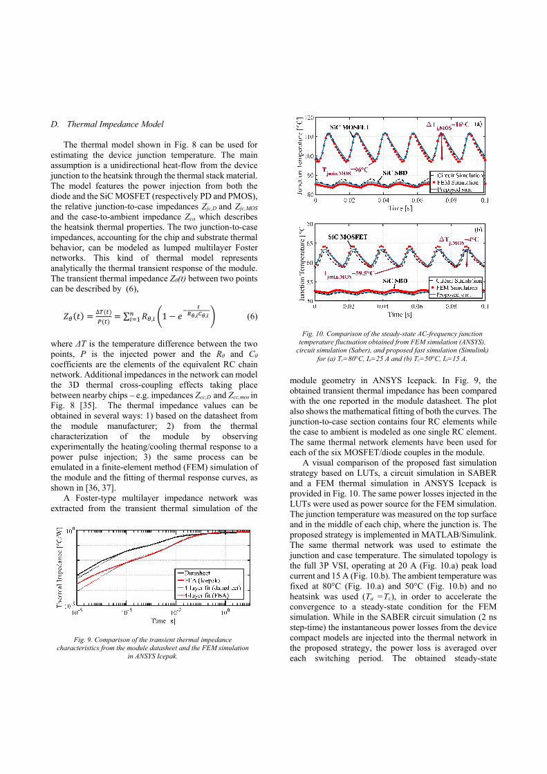
A visual comparison of the proposed fast simulation strategy based on LUTs, a circuit simulation in SABER and a FEM thermal simulation in ANSYS Icepack is provided in Fig. 10. The same power losses injected in the LUTs were used as power source for the FEM simulation. The junction temperature was measured on the top surface and in the middle of each chip, where the junction is. The proposed strategy is implemented in MATLAB/Simulink. The same thermal network was used to estimate the junction and case temperature. The simulated topology is the full 3P VSI, operating at 20 A (Fig. 10.a) peak load current and 15 A (Fig. 10.b). The ambient temperature was fixed at 80°C (Fig. 10.a) and 50°C (Fig. 10.b) and no heatsink was used (Ta =Tc), in order to accelerate the convergence to a steady-state condition for the FEM simulation. While in the SABER circuit simulation (2 ns step-time) the instantaneous power losses from the device compact models are injected into the thermal network in the proposed strategy, the power loss is averaged over each switching period. The obtained steady-state
Fig. 9. Comparison of the transient thermal impedance characteristics from the module datasheet and the FEM simulation
in ANSYS Icepak.
Fig. 10. Comparison of the steady-state AC-frequency junction temperature fluctuation obtained from FEM simulation (ANSYS),
circuit simulation (Saber), and proposed fast simulation (Simulink) for (a) Tc=80°C, Io=25 A and (b) Tc=50°C, Io=15 A.

temperature estimation shows outstanding agreement between the three simulation strategies, proving that the accuracy loss originating from the use of LUTs is not particularly significant. While the circuit simulation took about 7 min to converge and the FEM simulation about 10 min (1 ms step-time), the proposed simulation strategy only took about 5 s (100 µs step-time). This represents a huge gain in computational speed.
Each combination of Ta and Io throughout the mission profile, results in a different steady-state junction temperature Tj cycling for the device. It is assumed here that the steady-state lasts for the whole mission-profile sampling time step, before the operating conditions change. This assumption is legit, since the thermal time constant (seconds) is generally much shorter than the slow changes occurring in the mission profile.
The thermal behaviors of both MOSFET and diode have been mapped simulating the inverter operation for each combination of Ta and Io, in the same grid used to map the mission profile. The simulation was performed using the proposed approach in MATLAB/Simulink. A case to ambient thermal impedance of 0.3 K/W was used to model the heatsink. Therefore, the case temperature is not assumed constant in the mapping process. The steady-state minimum junction temperature Tj,min and thermal cycle amplitude ΔTj (defined as shown in Fig. 10) for each of the operating points were collected in 2D maps, plotted in Fig. 11. Hence, the maps are used as LUTs and
interpolated to determine the thermal stress on MOSFET and SBD for each point of the mission profile.
It is worth to note that the whole mapping of the steady-state thermal stress conditions takes about 2 minutes simulation time, with the chosen grid. This time might increase in case a finer mapping grid is used, or decrease in the opposite case, since the number of simulations required is changing.
Once the Tj,min and ΔTj for the whole mission have been calculated, the consumed lifetime or damage for each time-step can be predicted by using a lifetime model. The damage can be accumulated to calculate the overall consumed lifetime. The chosen reliability model will be presented in the next section.
E. Lifetime modeling and damage accumulation
Several studies have investigated the reliability of power modules by using accelerated test methods. A large number of IGBT modules was tested across a wide range of conditions during the LESIT project [38], providing an extensive data set for thermal reliability analysis of bond wires. The data is fitted by means of (7), a simple empirical equation, similar to the Coffin-Manson one used in [14], used to calculate the number of cycles to failure Nf under a certain stress condition.
∙ ∆ exp (7)
The equation contains the dependence on the junction
temperature cycle amplitude ΔTj and the mean junction temperature Tjm. Ea is the activation energy, kb is the Boltzmann constant and A and α are curve fitting parameters. A more recent and refined empirical model (widely known as the “Bayerer’s model”) was presented in [24], featuring the impact of the heating time ton, the current per wire I, the blocking voltage V and the wire diameter d. In addition, the minimum junction temperature Tj,min is considered. All the β coefficients are empirical and derived from curve fitting.
∙ ∆ ∙ exp,
∙ ∙ ∙ ∙ (8)
The modules used in the accelerated testing have rating
and technology comparable to the one in our case study. This model offers tolerance margins for each of the parameters, which can be useful for the overall error calculation of the proposed method. Therefore, the model shown in (8) is applied in this study.
A linear cumulative damage model, i.e. the Miner’s rule (9), is used for the lifetime prediction. The assumption of this model is that the damage on the modules is
Fig. 11. Thermal stress condition mapping for AC thermal cycling: minimum junction temperature (a) and thermal cycle amplitude (b) for the MOSFET; minimum junction temperature (c) and thermal
cycle amplitude (d) for the SBD.

independent of the stresses experienced during its life cycle [39].
∑ (9)
Where ni is the number of temperature cycles the
device spent under a certain stress condition and Nfi the number of cycles to failure under the same stress.
The thermal stress on power modules has basically two sources: the ambient temperature fluctuation and the variation of load condition for the power devices. The first causes a slow thermal cycling, with dynamics in the minute-range timescale, whereas the second causes a fast thermal cycling, usually in the sub-second timescale, e.g. at line frequency. According to the study in [40], the degradation of bond-wires heavily depends on the fast thermal cycling stress, whereas the slower dynamics, due to ambient temperature variations, affect the die-attach. It has been demonstrated in [17] that the low slow thermal cycling has minimum role in the lifetime consumption calculation for bond-wires. Including the consumed lifetime calculation due to die-attach degradation would require an additional cycle counting algorithm and
therefore, it has not been included in this study for conciseness.
Using the model in (8), the line-frequency thermal cycling consumed lifetime has been calculated and accumulated using the Miner’s rule. Tab. III reports the estimated damage on the bond-wires of both SiC MOSFET and SBD after one-year for both the considered MPs. The chosen heatsink thermal impedance in this case was 0.25 K/W.
As expected, the low thermal stress on the SBD chips results in a very low accumulated damage. Thus, the MOSFET chips’ bond-wires are the ones experiencing most of the aging. Additionally, MP-B, despite being quite similar to MP-A, shows significantly lower impact on the device lifetime.
It is interesting to observe how the resolution (time-step) used in MP-A affects the simulation time and the resulting damage prediction. Fig. 12.a shows that decreasing MP-A resolution (i.e. increasing the time-step) from 1 min to 1-2 hours does not significantly influence the damage prediction, while drastically reducing the simulation time from 5 min to around 10 s. However, further decrease in the resolution determines less accurate predictions. Moreover, a trade-off between accuracy and simulation time can be obtained by choosing a proper grid resolution for the mapping of the thermal stress (as in Fig. 11). As one can observe in Fig. 12.b, increasing the number of grid elements, i.e. the mapping resolution, beyond approximately 50, does not affect the lifetime prediction, while visibly increasing the simulation time. Additionally, the consumed lifetime has been calculated for a range of different operating conditions. Fig. 13 shows how the variation of the switching frequency and the heatsink thermal impedance affects the damage prediction for both the MPs. This kind of comparative analysis can be easily performed using the proposed strategy. Reliability-wise optimization of a certain design in respect to one or more parameters is possible in relatively short simulation time and can also be automated.
Fig. 12. Impact of MP resolution (a) and of thermal stress mapping resolution (b) on the 1-year damage prediction and the
simulation time for MP-A.
TABLE III – 1-YEAR ACCUMULATED DAMAGE
SiC MOSFET bond-wire damage
SiC SBD bond-wire damage
MP-A 0.026 (2.6 %) <10-2 % MP-B 0.01 (1 %) <10-2 %
Fig. 13. Impact of the switching frequency on the 1-year damage prediction for MP-A (a) and MP-B (b).

IV. DISCUSSION
It is worth to note that the predicted lifetime consumption only concerns the bond-wires degradation, which is only part of the damage accumulated by the module. Many failure mechanisms contribute to the end-of-life of a power module, including damage due to single abnormal events, e.g. short circuit or overvoltage, which could occur during the device lifetime. The module’s lifetime depends on the accumulation of the damage resulting from each of these failure mechanisms. Absolute life prediction is hard and involves a great number of uncertainties. Calculating the estimation error in the electrical and thermal models is possible, while it is more difficult to identify the tolerance for a lifetime prediction and goes beyond the scope of this work. The results provided in this analysis should therefore been taken as an indicator of the factors involved in the lifetime estimation process and the demonstration of a fast prediction strategy resulting from accurate electro-thermal modeling for the device, the module and the topology. Nevertheless, the final consumed lifetime prediction can be rather useful when comparing different design solutions and evaluating the one with the best reliability performance for the given mission profile. In these terms, the presented strategy can boost the reliable design of power electronic systems.
The degradation of several parameters takes place during the lifetime of a power module. The package-related degradation mostly influences the die and bond-wire attach. The chip also undergoes aging, which results in increased gate voltage threshold. The influence of such degradation on the considered SiC module was measured in [25], while in [41] the drift of on-state voltage for bond-wire and chip was measured separately during accelerated tests. Whether this degradation should be taken into account or not in the simulation process, depends on the entity of the on-state voltage drift, which could worsen the power loss generation. In the case considered here, the consumed lifetime during the mission profile is so low that the impact of parameter degradation on the loss would be, in total, less than 1%. When applying longer or more severe loading to the device, this degradation should be taken into account. The influence of parameter variation on the lifetime is estimated in [17] through Monte Carlo analysis.
V. CONCLUSION
A fast lifetime prediction strategy for the bond-wire
interconnections of power semiconductor modules has been explored and presented in detail in this paper. An accurate physics-based electrical device model and thermal network have enabled an offline mapping of power losses and thermal behavior for a 1.2 kV three-
phase SiC power MOSFET/Schottky diode module. The temperature-dependent power losses have been validated through experimental data. A case study with a 20 kW PV inverter has been presented for the chosen module in order to clarify the proposed method application, in which the consumed lifetime due to the bond-wire degradation has been calculated for two different 1-year PV mission profiles. The use of LUTs has allowed the fast simulation of very large timescales in few minutes without compromising the accuracy and the comparative analysis of different design solutions. The proposed methodology can help the designer to assess the reliability of a power module and can be extended to any commercial device, provided the availability of proper technical documentation. Moreover, the process can be easily iterated to perform an automated optimization and extended to consider additional failure mechanisms. This strategy may be used for selecting among different part-numbers, optimizing in terms of electro-thermal performances, reliability and cost-effectiveness.
ACKNOWLEDGEMENTS
The authors would like to thank the MSCAD research
group at the University of Arkansas, AR, USA, the Advanced Power Electronics Technology and Tools (APETT) project at Aalborg University, Aalborg, DK and Innovation Fund Denmark for their contribution and support in this work.
REFERENCES
[1] M. N. Yoder, “Wide bandgap semiconductor materials and
devices,” IEEE Trans. Electron Devices, vol. 43, no. 10, pp. 1633–1636, Oct. 1996.
[2] P. G. Neudeck, R. S. Okojie, and L.-Y. Chen, “High-temperature electronics - a role for wide bandgap semiconductors?,” in Proc. of IEEE, vol. 90, no. 6, pp. 1065–1076, Jun. 2002.
[3] S. Hazra et al., “High Switching Performance of 1700-V, 50-A SiC Power MOSFET Over Si IGBT/BiMOSFET for Advanced Power Conversion Applications,” IEEE Trans. Power Electron., vol. 31, no. 7, pp. 4742–4754, Jul. 2016.
[4] J. W. Palmour, “Silicon carbide power device development for industrial markets,” in Proc. of IEEE International Electron Devices Meeting, pp. 111-118, 2014.
[5] J. A. Cooper, M. R. Melloch, R. Singh, A. Agarwal, and J. W. Palmour, “Status and prospects for SiC power MOSFETs,” IEEE Trans. Electron Devices, vol. 49, no. 4, pp. 658–664, Apr. 2002.
[6] K. Ma, H. Wang, and F. Blaabjerg, “New Approaches to Reliability Assessment: Using physics-of-failure for prediction and design in power electronics systems,” IEEE Power Electron. Mag., vol. 3, no. 4, pp. 28–41, Dec. 2016.
[7] H. Wang, M. Liserre, and F. Blaabjerg, “Toward Reliable Power Electronics: Challenges, Design Tools, and Opportunities,” IEEE Ind. Electron. Mag., vol. 7, no. 2, pp. 17–26, Jun. 2013.
[8] B. Gu, J. Dominic, J. S. Lai, C. L. Chen, T. LaBella, and B. Chen, “High Reliability and Efficiency Single-Phase Transformerless Inverter for Grid-Connected Photovoltaic Systems,” IEEE Trans. Power Electron., vol. 28, no. 5, pp. 2235–2245, May 2013.

[9] Military Handbook: Reliability Prediction of Electronic Equipment, Standard MIL-HDBK-217F. 1991.
[10] FIDES Guide 2009 Edition: A Reliability Methodology for Electronic Systems. 2010.
[11] K. Ma and F. Blaabjerg, “Multi-timescale modelling for the loading behaviours of power electronics converter,” in Proc. of IEEE Energy Conversion Congress and Exposition (ECCE), pp. 5749–5756, 2015.
[12] K. Ma, M. Liserre, F. Blaabjerg, and T. Kerekes, “Thermal Loading and Lifetime Estimation for Power Device Considering Mission Profiles in Wind Power Converter,” IEEE Trans. Power Electron., vol. 30, no. 2, pp. 590–602, Feb. 2015.
[13] S. E. D. León-Aldaco, H. Calleja, F. Chan, and H. R. Jiménez-Grajales, “Effect of the Mission Profile on the Reliability of a Power Converter Aimed at Photovoltaic Applications: A Case Study,” IEEE Trans. Power Electron., vol. 28, no. 6, pp. 2998–3007, Jun. 2013.
[14] M. Ciappa, F. Carbognani, and W. Fichtner, “Lifetime modeling of thermomechanics-related failure mechanisms in high power IGBT modules for traction applications,” in Proc. of IEEE 15th International Symposium on Power Semiconductor Devices and IC. ISPSD, pp. 295–298, 2003.
[15] Z. Zhou, M. S. Khanniche, P. Igic, S. T. Kong, M. Towers, and P. A. Mawby, “A fast power loss calculation method for long real time thermal simulation of IGBT modules for a three-phase inverter system,” in Proc. of 2005 European Conference on Power Electronics and Applications , 2005.
[16] A. T. Bryant, P. A. Mawby, P. R. Palmer, E. Santi, and J. L. Hudgins, “Exploration of Power Device Reliability Using Compact Device Models and Fast Electrothermal Simulation,” IEEE Trans. Ind. Appl., vol. 44, no. 3, pp. 894–903, May 2008.
[17] P. D. Reigosa, H. Wang, Y. Yang, and F. Blaabjerg, “Prediction of Bond Wire Fatigue of IGBTs in a PV Inverter Under a Long-Term Operation,” IEEE Trans. Power Electron., vol. 31, no. 10, pp. 7171–7182, Oct. 2016.
[18] A. S. Bahman, F. Iannuzzo, and F. Blaabjerg, “Mission-profile-based stress analysis of bond-wires in SiC power modules,” Microelectron. Reliab., vol. 64, pp. 419–424, Sep. 2016.
[19] C. Sintamarean, F. Blaabjerg, H. Wang, and Y. Yang, “Real field mission profile oriented design of a SiC-based PV-inverter application,” in Proc. of 2013 IEEE Energy Conversion Congress and Exposition, pp. 940–947, 2013.
[20] Z. Qiu, J. Zhang, P. Ning, and X. Wen, “Reliability modeling and analysis of SiC MOSFET power modules,” in Proc. of IECON 2017 - 43rd Annual Conference of the IEEE Industrial Electronics Society, pp. 1459–1463, 2017.
[21] V. Smet et al., “Ageing and Failure Modes of IGBT Modules in High-Temperature Power Cycling,” IEEE Trans. Ind. Electron., vol. 58, no. 10, pp. 4931–4941, Oct. 2011.
[22] R. Schmidt and U. Scheuermann, “Separating Failure Modes in Power Cycling Tests,” in Proc. of the 7th International Conference on Integrated Power Electronics Systems (CIPS), pp. 1–6, 2012.
[23] L. Yang, P. A. Agyakwa, and C. M. Johnson, “Physics-of-Failure Lifetime Prediction Models for Wire Bond Interconnects in Power Electronic Modules,” IEEE Trans. Device Mater. Reliab., vol. 13, no. 1, pp. 9–17, Mar. 2013.
[24] R. Bayerer, T. Herrmann, T. Licht, J. Lutz, and M. Feller, “Model for Power Cycling lifetime of IGBT Modules - various factors influencing lifetime,” in Proc. of 5th International Conference on Integrated Power Electronics Systems, 2008.
[25] H. Luo, F. Iannuzzo, F. Blaabjerg, M. Turnaturi, and E. Mattiuzzo, “Aging precursors and degradation effects of SiC-MOSFET modules under highly accelerated power cycling conditions,” in Proc. of 2017 IEEE Energy Conversion Congress and Exposition (ECCE), pp. 2506–2511, 2017.
[26] H. A. Mantooth and A. R. Hefner, “Electrothermal simulation of an IGBT PWM inverter,” IEEE Trans. Power Electron., vol. 12, no. 3, pp. 474–484, May 1997.
[27] Y. C. Gerstenmaier, A. Castellazzi, and G. K. M. Wachutka, “Electrothermal simulation of multichip-modules with novel transient thermal model and time-dependent boundary conditions,” IEEE Trans. Power Electron., vol. 21, no. 1, pp. 45–55, Jan. 2006.
[28] A. Castellazzi and M. Ciappa, “Multi-level electro-thermal modeling for circuit simulation of packaged power devices,” in Proc. of 2008 11th Workshop on Control and Modeling for Power Electronics, 2008.
[29] C. Sintamarean, F. Blaabjerg, and H. Wang, “A novel electro-thermal model for wide bandgap semiconductor based devices,” in Proc. of 2013 15th European Conference on Power Electronics and Applications (EPE), 2013.
[30] L. Wei, R. J. Kerkman, and R. A. Lukaszewski, “Evaluation of Power Semiconductors Power Cycling Capabilities for Adjustable Speed Drive,” in Proc. of 2008 IEEE Industry Applications Society Annual Meeting, 2008.
[31] L. Ceccarelli, A. S. Bahman, F. Iannuzzo, and F. Blaabjerg, “A Fast Electro-Thermal Co-Simulation Modeling Approach for SiC Power MOSFETs,” in Proc. of the 32nd IEEE Applied Power Electronics Conference and Exposition, Tampa, USA, 2017, pp. 966–973.
[32] Datasheet, “https://www.wolfspeed.com/ccs020m12cm2”, 2014. [33] MSCAD, “SiC Power MOSFET Compact Model:
https://mscad.uark.edu/compact-models.” University of Arkansas, Aug. 2016.
[34] T. R. McNutt, A. R. Hefner, H. A. Mantooth, D. Berning, and S. H. Ryu, “Silicon Carbide Power MOSFET Model and Parameter Extraction Sequence,” IEEE Trans. Power Electron., vol. 22, no. 2, pp. 353–363, Mar. 2007.
[35] A. S. Bahman, K. Ma, and F. Blaabjerg, “Thermal impedance model of high power IGBT modules considering heat coupling effects,” in Proc. of 2014 International Power Electronics and Application Conference and Exposition, Shanghai, China, pp. 1382–1387, 2014.
[36] A. S. Bahman, K. Ma, and F. Blaabjerg, “General 3D lumped thermal model with various boundary conditions for high power IGBT modules,” in 2016 IEEE Applied Power Electronics Conference and Exposition (APEC), pp. 261–268, 2016.
[37] K. Ma, A. S. Bahman, S. Beczkowski, and F. Blaabjerg, “Complete Loss and Thermal Model of Power Semiconductors Including Device Rating Information,” IEEE Trans. Power Electron., vol. 30, no. 5, pp. 2556–2569, May 2015.
[38] M. Held, P. Jacob, G. Nicoletti, P. Scacco And, and M.-H. Poech, “Fast power cycling test for insulated gate bipolar transistor modules in traction application,” Int. J. Electron., vol. 86, no. 10, pp. 1193–1204, Oct. 1999.
[39] M. A. Miner, “Cumulative Damage in Fatigue,” J. of Appl. Mech ., 1945, vol. 12, pp. 159–164.
[40] IEC 60749-34:2010, https://webstore.iec.ch/publication/3381, 2010.
[41] N. Baker, H. Luo, and F. Iannuzzo, “Simultaneous On-State Voltage and Bond-Wire Resistance Monitoring of Silicon Carbide MOSFETs,” Energies, vol. 10, no. 3, p. 384, Mar. 2017.