aalto- integrated circuits for dd linear and efficient
TRANSCRIPT

9HSTFMG*afjdad+
ISBN 978-952-60-5930-3 (printed) ISBN 978-952-60-5931-0 (pdf) ISSN-L 1799-4934 ISSN 1799-4934 (printed) ISSN 1799-4942 (pdf) Aalto University School of Electrical Engineering Department of Micro- and Nanosciences www.aalto.fi
BUSINESS + ECONOMY ART + DESIGN + ARCHITECTURE SCIENCE + TECHNOLOGY CROSSOVER DOCTORAL DISSERTATIONS
Aalto-D
D 17
0/2
014
This dissertation presents advances related to the integration of high-Q resonators, DC-DC converters, and programmable RF front-ends for cellular receivers. These three building blocks have traditionally required implementations that are partly external to the integrated circuit, thus increasing system size, cost, and complexity. The trend towards versatile multi-standard operation and software-defined radios calls instead for compact solutions that are integrable, programmable, and even reconfigurable. The dissertation presents five integrated circuit implementations that attempt to raise the integration level while maintaining receiver performance.
Kim
Östm
an Integrated C
ircuits for Linear and E
fficient Receivers
Aalto
Unive
rsity
Department of Micro- and Nanosciences
Integrated Circuits for Linear and Efficient Receivers
Kim Östman
DOCTORAL DISSERTATIONS

Aalto University publication series DOCTORAL DISSERTATIONS 170/2014
Integrated Circuits for Linear and Efficient Receivers
Kim Östman
A doctoral dissertation completed for the degree of Doctor of Science (Technology) to be defended, with the permission of the Aalto University School of Electrical Engineering, at a public examination held at the lecture hall S1 of the school on 5 December 2014 at 12.
Aalto University School of Electrical Engineering Department of Micro- and Nanosciences

Supervising professor Prof. Jussi Ryynänen Thesis advisor Dr. Kari Stadius Preliminary examiners Prof. Antonio Liscidini, University of Toronto, Canada Dr. Sven Mattisson, Ericsson, Sweden Opponent Dr. Aarno Pärssinen, University of Oulu, Finland
Aalto University publication series DOCTORAL DISSERTATIONS 170/2014 © Kim Östman ISBN 978-952-60-5930-3 (printed) ISBN 978-952-60-5931-0 (pdf) ISSN-L 1799-4934 ISSN 1799-4934 (printed) ISSN 1799-4942 (pdf) http://urn.fi/URN:ISBN:978-952-60-5931-0 Unigrafia Oy Helsinki 2014 Finland

Abstract Aalto University, P.O. Box 11000, FI-00076 Aalto www.aalto.fi
Author Kim Östman Name of the doctoral dissertation Integrated Circuits for Linear and Efficient Receivers Publisher School of Electrical Engineering Unit Department of Micro- and Nanosciences
Series Aalto University publication series DOCTORAL DISSERTATIONS 170/2014
Field of research Electronic circuit design
Manuscript submitted 25 August 2014 Date of the defence 5 December 2014
Permission to publish granted (date) 21 October 2014 Language English
Monograph Article dissertation (summary + original articles)
Abstract This dissertation presents original research contributions in the form of five integrated
circuit (IC) implementations and seven scientific publications. They present advances related to high-Q resonators, DC-DC converters, and programmable RF front-ends for integrated wireless receivers. Because these three building blocks have traditionally required implementations that are partly external to the IC, the ultimate target is to reduce system size, cost, and complexity. Wireless receivers utilize high-Q resonators for accurate frequency synthesis and signal filtering, typically by relying on external quartz resonators and rigid surface acoustic wave filters. The above-IC implementation of bulk acoustic wave (BAW) resonators and the use of programmable on-chip N-path filtering offer interesting integrable alternatives. Accordingly, this dissertation demonstrates a 2.1-GHz voltage controlled oscillator (VCO) in 250-nm SiGe:C BiCMOS, based on an above-IC BAW resonator. Furthermore, N-path filtering is investigated in a 2.5-GHz narrowband RF front-end in 40-nm CMOS. It achieves more than 10 dB of interferer filtering early in the RF chain, and the original analysis details the counter-intuitive behavior of the N-path filter when it is used together with LC-based filters. Receiver power management requires the use of step-down DC-DC converters between the external battery and the integrated receiver circuitry. The related switching regulators are typically based on low-frequency operation, which requires external filtering components. In contrast, this dissertation presents a fully integrated 3.6-to-1.8-V buck converter in 65-nm CMOS that uses switching frequencies of more than 100 MHz. A topology-independent switch bridge optimization approach is also proposed. The measurement results demonstrate the feasibility of integration, although with compromised performance. Finally, the software-defined radio paradigm operates on the premise of radio and RF front-end programmability. This calls for A/D conversion as close to the antenna interface as possible. This dissertation presents original work on a 40-nm CMOS direct delta-sigma receiver (DDSR) for the 0.7-to-2.7-GHz frequency range. Particular emphasis is put on developing new methods for DDSR RF front-end modeling and design.
Keywords bulk acoustic wave resonator, direct delta-sigma receiver, low noise amplifier, quality factor, radio receiver, voltage controlled oscillator
ISBN (printed) 978-952-60-5930-3 ISBN (pdf) 978-952-60-5931-0
ISSN-L 1799-4934 ISSN (printed) 1799-4934 ISSN (pdf) 1799-4942
Location of publisher Helsinki Location of printing Helsinki Year 2014
Pages 185 urn http://urn.fi/URN:ISBN:978-952-60-5931-0


Tiivistelmä Aalto-yliopisto, PL 11000, 00076 Aalto www.aalto.fi
Tekijä Kim Östman Väitöskirjan nimi Mikropiirejä lineaarisiin ja tehokkaisiin vastaanottimiin Julkaisija Sähkötekniikan korkeakoulu Yksikkö Mikro- ja nanotekniikan laitos
Sarja Aalto University publication series DOCTORAL DISSERTATIONS 170/2014
Tutkimusala Piiritekniikka
Käsikirjoituksen pvm 25.08.2014 Väitöspäivä 05.12.2014
Julkaisuluvan myöntämispäivä 21.10.2014 Kieli Englanti
Monografia Yhdistelmäväitöskirja (yhteenveto-osa + erillisartikkelit)
Tiivistelmä Tässä väitöskirjassa esitellään viiteen mikropiiriin ja seitsemään tieteelliseen julkaisuun
sisältyviä tutkimustuloksia, jotka keskittyvät integroituihin langattomiin vastaanottimiin. Ne liittyvät korkean hyvyysluvun resonaattoreihin, DC-DC -muuntimiin ja ohjelmoitaviin RF-etupäihin. Koska näiden kolmen lohkon toteutus on perinteisesti vaatinut ulkoisia komponentteja, tässä työssä esitetyt tulokset tähtäävät vastaanottimen koon, hinnan ja monimutkaisuuden vähentämiseen. Langattomat vastaanottimet hyödyntävät korkean hyvyysluvun resonaattoreita tarkkaan taajuussynteesiin ja signaalien suodattamiseen. Tyypillisesti tämä perustuu ulkoisille kideresonaattoreille ja pinta-aaltosuotimille. Mikropiirin päälle toteutettavat massa-aaltoresonaattorit ja ohjelmoitavat monitiesuodattimet tarjoavat mielenkiintoisia integroitavia vaihtoehtoja. Massa-aaltoresonaattoria hyödynnetään tässä työssä 2,1 GHz:n alueelle tarkoitetussa jänniteohjatussa oskillaattorissa, joka on toteutettu 250 nm:n SiGe:C BiCMOS-teknologialla. Monitiesuodatusta tutkitaan 2,5 GHz:n RF-etupäässä, joka on toteutettu 40 nm:n CMOS-teknologialla. Sillä saavutetaan yli 10 dB:n häiriösuodatus, ja aiheesta esitetty alkuperäisanalyysi tarkastelee monitiesuodattimen ja LC-suodattimen yhdistämiseen liittyvää käyttäytymistä. Vastaanottimissa käytetään DC-DC -muuntimia sovittamaan ulkoisen akun korkea jännite mikropiirin tarvitsemalle tasolle. Tässä käytetyt matalataajuiset hakkurimuuntimet tarvitsevat yleensä ulkoisia komponentteja. Tässä väitöskirjassa esitellään 65 nm:n CMOS-teknologialla toteutettu hakkurimuunnin, joka puolittaa 3,6 voltin akkujännitteen yli 100 MHz:n kytkentätaajuutta käyttäen. Tähän liittyen esitellään myös tarkasta toteutustavasta riippumaton optimointimenetelmä. Mittaustulokset osoittavat muuntimen integroinnin olevan mahdollista, mutta toimintatehokkuudessa joudutaan tekemään kompromisseja. Ohjelmistoradio nojaa ajatukseen radion ja RF-etupään ohjelmoitavuudesta. Analogia-digitaali -muunnos olisi siksi hyvä tehdä mahdollisimman lähellä antennirajapintaa. Tähän aiheeseen liittyen väitöskirjan viimeinen osio esittelee uusia mallinnus- ja suunnittelumenetelmiä nk. delta-sigma -suoramuunnosvastaanottimen RF-etupäälle. Lisäksi esitellään 40 nm:n CMOS-teknologialla tehty toteutus 0,7-2,7 GHz:n taajuusalueelle.
Avainsanat delta-sigma -suoramuunnosvastaanotin, hyvyysluku, jänniteohjattu oskillaattori, massa-aaltoresonaattori, radiovastaanotin, vähäkohinainen vahvistin
ISBN (painettu) 978-952-60-5930-3 ISBN (pdf) 978-952-60-5931-0
ISSN-L 1799-4934 ISSN (painettu) 1799-4934 ISSN (pdf) 1799-4942
Julkaisupaikka Helsinki Painopaikka Helsinki Vuosi 2014
Sivumäärä 185 urn http://urn.fi/URN:ISBN:978-952-60-5931-0


Preface
This dissertation is based on work that was done at the Radio-Frequency
Communication Circuits Laboratory of Tampere University of Technology
and at the Electronic Circuit Design Unit of Aalto University. The work
was executed in project arrangements that were financed by the Euro-
pean Union ("MARTINA"), Infineon Technologies AG, the ENIAC Joint
Undertaking ("ARTEMOS"), and the Academy of Finland ("UNIRADIO").
I have also been supported financially by the Finnish Graduate School
in Electronics, Telecommunications and Automation (GETA) and by the
Finnish Cultural Foundation, for which I express my sincere gratitude.
On a more personal note, I would like to thank Prof. Nikolay T. Tchamov,
with whom I began the journey towards this dissertation at Tampere Uni-
versity of Technology. He guided the first part of my research, and taught
me a number of professional skills that continue to serve me well. I would
also like to thank Prof. Jussi Ryynänen, who took over as my supervi-
sor when I began working at Aalto University in 2011. I have especially
valued his cheerful attitude, along with his willingness to entertain new
initiatives and to encourage their timely execution. My instructor Dr.
Kari Stadius is warmly acknowledged for his keen eye for detail, and for
shedding light on many things that were previously a mystery to me. I
also thank Prof. Antonio Liscidini and Dr. Sven Mattisson for serving as
pre-examiners of this dissertation, and for giving constructive suggestions
that helped me to improve its quality. Dr. Aarno Pärssinen kindly agreed
to serve as the opponent, for which I thank him highly.
I would also like to express appreciation for my colleagues at Tampere
University of Technology and at Aalto University. I have had the fortune
of working with really talented people, and the brainstorming and criti-
cisms have been of utmost importance. Mr. Sami Sipilä, Mr. Jani Järven-
haara, and Mr. Mikko Englund were my closest co-workers in our design
1

Preface
projects, and they were a joy to work with. Dr. Mikko Kaltiokallio, Mr.
Tero Tikka, and Mr. Olli Viitala provided invaluable practical assistance,
and Mikko is particularly acknowledged for teaching me receiver design.
Antti, Hans, Hristo, Ismo, Ivan, Johanna, Joni, Juho, Mihail, Pekko, Sve-
tozar, Tapio, Ville, and Yury are other close co-workers whose company
I have enjoyed through coffee break laughs, interesting discussions, and
practical help. My thanks also go to the great colleagues I had at the
Finnish Higher Education Evaluation Council in 2010–2011, and to my
current colleagues at Nokia Technologies.
Free-time interests are not to be forgotten, and I particularly acknowl-
edge the teams at OH4A and "Radio Arcala," OH8X. Radio amateur activ-
ities, competitions in particular, have been a lot of fun, and being part of
these teams has provided me with a host of previously unimaginable op-
portunities. These activities also serve as a useful practical complement
to my professional interests. After all, what could be more educational
than slamming your headphones on the table in disgust in the wee hours
of the morning, after actually experiencing what it is like for a "blocker" to
turn up and bury sensitivity-level Morse code under spurious emissions?
My warmest thanks go to my parents Bertel and Ruusa, and to my sis-
ter Anne-Maria with her family. They have always been supportive of
my pursuits, and the closeness of these relationships has provided a won-
derful foundation on which to build. My father and paternal grandfather
were both employed in the field of electrical engineering and I’m happy to
take that tradition forward, albeit in mV instead of kV.
Having now completed doctoral work both in the humanities and in mi-
croelectronics, I wish I could say that I have "seen the light." I cannot,
but I’m happy to have experienced two such different worlds and to have
forged invaluable relationships in both of them. Very different languages
are spoken, but human curiosity and the innate desire for greater things
burn bright in both. Indeed, we all keep wanting to discover that elusive
"final breakthrough," while complaining about bureaucracy, long review
times, and insufficient funding on the way!
Sunnyvale, California, October 27, 2014,
Kim Östman
2

Contents
Preface 1
Contents 3
List of Publications 5
Author’s Contribution 7
List of Abbreviations 9
List of Symbols 13
1. Introduction 17
1.1 Background . . . . . . . . . . . . . . . . . . . . . . . . . . . . 17
1.2 Objective of this work . . . . . . . . . . . . . . . . . . . . . . . 18
1.3 Contents and organization of the dissertation . . . . . . . . . 19
1.4 Main scientific merits . . . . . . . . . . . . . . . . . . . . . . . 20
2. Integrated Radio Receivers 23
2.1 Overview . . . . . . . . . . . . . . . . . . . . . . . . . . . . . . 23
2.2 Performance metrics . . . . . . . . . . . . . . . . . . . . . . . 28
2.3 Performance requirements . . . . . . . . . . . . . . . . . . . . 34
2.4 Major implementation challenges . . . . . . . . . . . . . . . . 39
3. High-Q Component Integration 43
3.1 Overview . . . . . . . . . . . . . . . . . . . . . . . . . . . . . . 43
3.2 Bulk Acoustic Wave resonators . . . . . . . . . . . . . . . . . 45
3.3 N-path filters . . . . . . . . . . . . . . . . . . . . . . . . . . . . 49
3.4 Experimental work . . . . . . . . . . . . . . . . . . . . . . . . 53
3.4.1 Receiver front-end . . . . . . . . . . . . . . . . . . . . . 53
3.4.2 FBAR oscillator . . . . . . . . . . . . . . . . . . . . . . 59
3

Contents
4. Power Management 65
4.1 Overview . . . . . . . . . . . . . . . . . . . . . . . . . . . . . . 65
4.2 Buck converter characteristics . . . . . . . . . . . . . . . . . . 68
4.3 Experimental work . . . . . . . . . . . . . . . . . . . . . . . . 72
5. Radio-Frequency Front-End 77
5.1 Overview . . . . . . . . . . . . . . . . . . . . . . . . . . . . . . 77
5.2 Main architectures . . . . . . . . . . . . . . . . . . . . . . . . 79
5.2.1 LNA-first front-ends . . . . . . . . . . . . . . . . . . . 79
5.2.2 Mixer-first front-ends . . . . . . . . . . . . . . . . . . . 83
5.3 Direct delta-sigma receiver . . . . . . . . . . . . . . . . . . . . 84
5.4 Experimental work . . . . . . . . . . . . . . . . . . . . . . . . 92
6. Conclusions 99
Bibliography 103
Publications 119
4

List of Publications
This thesis consists of an overview and of the following publications which
are referred to in the text by their Roman numerals.
I K. B. Östman, S. T. Sipilä, I. S. Uzunov, and N. T. Tchamov. Novel VCO
Architecture Using Series Above-IC FBAR and Parallel LC Resonance.
IEEE Journal of Solid-State Circuits, vol. 41, no. 10, pp. 2248–2256,
Oct. 2006.
II K. B. Östman and M. Valkama. Start-Up Robustness Against Resonator-
Qs Defects in a 2-GHz FBAR VCO. In Proceedings of the IEEE Interna-
tional Frequency Control Symposium, Baltimore, MD, USA, pp. 281–
284, May 2012.
III K. B. Östman, J. K. Järvenhaara, S. S. Broussev, and I. Viitaniemi. A
3.6-to-1.8-V Cascode Buck Converter With a Stacked LC Filter in 65-nm
CMOS. IEEE Transactions on Circuits and Systems II: Express Briefs,
vol. 61, no. 4, pp. 234–238, Apr. 2014.
IV K. B. Östman, M. Englund, O. Viitala, K. Stadius, K. Koli, and J.
Ryynänen. Characteristics of LNA Operation in Direct Delta-Sigma Re-
ceivers. IEEE Transactions on Circuits and Systems II: Express Briefs,
vol. 61, no. 2, pp. 70–74, Feb. 2014.
V K. B. Östman, M. Englund, O. Viitala, K. Stadius, J. Ryynänen, and
K. Koli. Design Tradeoffs in N-path GmC Integrators for Direct Delta-
Sigma Receivers. In Proceedings of the European Conference on Circuit
5

List of Publications
Theory and Design, Dresden, Germany, pp. 1–4, Sept. 2013.
VI M. Englund, K. B. Östman, O. Viitala, M. Kaltiokallio, K. Stadius, K.
Koli, and J. Ryynänen. A Programmable 0.7-to-2.7GHz Direct ΔΣ Re-
ceiver in 40nm CMOS. In IEEE International Solid-State Circuits Con-
ference Digest of Technical Papers, San Francisco, CA, USA, pp. 470–
471, Feb. 2014.
VII K. B. Östman, M. Englund, O. Viitala, M. Kaltiokallio, K. Stadius, K.
Koli, and J. Ryynänen. A 2.5-GHz Receiver Front-End with Q-Boosted
Post-LNA N-Path Filtering in 40-nm CMOS. IEEE Transactions on Mi-
crowave Theory and Techniques, vol. 62, no. 9, pp. 2071–2083, Sept.
2014.
6

Author’s Contribution
Publication I: “Novel VCO Architecture Using Series Above-IC FBARand Parallel LC Resonance”
The author designed the two reported VCO circuits and was mainly re-
sponsible for writing the paper manuscript. The author measured the
circuits in collaboration with Mr. Sipilä. The theoretical analysis in Sec-
tion IV-C was performed and written by Dr. Uzunov. Prof. Tchamov
supervised the work.
Publication II: “Start-Up Robustness Against Resonator-Qs Defectsin a 2-GHz FBAR VCO”
The author performed all circuit analysis, wrote the paper manuscript,
and presented the paper. Prof. Valkama collaborated on the manuscript.
Publication III: “A 3.6-to-1.8-V Cascode Buck Converter With aStacked LC Filter in 65-nm CMOS”
The author designed the DC-DC converter circuit (switch bridge, LC out-
put filter, and driver chains), had the main responsibility for the reported
chip, performed all circuit analysis, and wrote the paper manuscript. Dr.
Broussev designed the pulse generation circuitry and measurement PCB.
The measurements were carried out collaboratively by all authors.
7
Author’s Contribution
Publication IV: “Characteristics of LNA Operation in DirectDelta-Sigma Receivers”
The author collaborated with Mr. Englund and Mr. Viitala on developing
the analytical system model. The author performed the circuit analysis
and wrote the paper manuscript. Mr. Englund performed the discrete-
time system-level simulations. Dr. Stadius, Dr. Koli, and Prof. Ryynänen
supervised the work.
Publication V: “Design Tradeoffs in N-path GmC Integrators forDirect Delta-Sigma Receivers”
The author performed all circuit analysis, wrote the paper manuscript,
and presented the paper. The author collaborated with Mr. Englund and
Mr. Viitala on developing the analytical system model. Dr. Stadius, Prof.
Ryynänen, and Dr. Koli supervised the work.
Publication VI: “A Programmable 0.7-to-2.7GHz Direct ΔΣ Receiverin 40nm CMOS”
The author designed the wideband and narrowband RF front-ends, in-
cluding the off-chip RF transmission lines, wrote a significant part of the
paper manuscript, and presented the paper. The author also assisted Mr.
Englund in the measurements of the complete receiver. Mr. Englund de-
signed the system and its baseband parts, whereas Mr. Viitala designed
the measurement PCB. Dr. Kaltiokallio assisted with the IC design work,
and Dr. Stadius, Dr. Koli, and Prof. Ryynänen supervised the work.
Publication VII: “A 2.5-GHz Receiver Front-End with Q-BoostedPost-LNA N-Path Filtering in 40-nm CMOS”
The author designed the RF front-end and the related off-chip RF trans-
mission lines, performed all circuit analysis and measurements, and wrote
the paper manuscript. Mr. Englund designed the baseband low-pass fil-
tering circuits. Mr. Viitala designed the measurement PCB. Dr. Kaltio-
kallio assisted with the IC design work, and Dr. Stadius, Dr. Koli, and
Prof. Ryynänen supervised the work.
8

List of Abbreviations
2G second generation
3G third generation
4G fourth generation
A/D analog-to-digital
AC alternating current
ADC analog-to-digital converter
AlN aluminum nitride
B–1dBCP blocker compression point
BAW bulk acoustic wave
BCP blocker compression point
BiCMOS bipolar complementary metal oxide semiconductor
BJT bipolar junction transistor
BNF blocker noise figure
BPF bandpass filter
BVD Butterworth Van Dyke
CB common-base
CC common-collector
CMOS complementary metal oxide semiconductor
CR cognitive radio
CT continuous time
D/A digital-to-analog
DC direct current
DDSR direct delta-sigma receiver
DSM delta-sigma modulator
DSP digital signal processing
DT discrete time
9

List of Abbreviations
EDGE Enhanced Data rates for GSM Evolution
EEF efficiency enhancement factor
F noise factor
FBAR film bulk acoustic resonator
FDD frequency-division duplexing
FIR finite impulse response
FS frequency synthesizer
GBVD generalized Butterworth Van Dyke
GSM Global System for Mobile Communications
I in-phase
I/O input-output
IC integrated circuit
ICP input compression point
IDAC current-mode digital-to-analog converter
IF intermediate frequency
IIP2 input-referred second-order intercept point
IIP3 input-referred third-order intercept point
IM2 second-order intermodulation product
IM3 third-order intermodulation product
ITU International Telecommunication Union
LDO low drop-out regulator
LNA low noise amplifier
LNTA low noise transconductance amplifier
LO local oscillator
LPF lowpass filter
LPTV linear periodically time-variant
LTE Long Term Evolution
LTE-A Long Term Evolution - Advanced
LTI linear time-invariant
MBVD modified Butterworth Van Dyke
MEMS microelectromechanical system
MOS metal oxide semiconductor
NF noise figure
NMOS n-type metal oxide semiconductor
NTF noise transfer function
10

List of Abbreviations
OSR oversampling ratio
PCB printed circuit board
PLL phase-locked loop
PMIC power management integrated circuit
PMOS p-type metal oxide semiconductor
PMU power management unit
PSRR power supply rejection ratio
Q quadrature
RF radio frequency
RFIC radio frequency integrated circuit
RHP right-hand plane
RX receiver
SAW surface acoustic wave
SDR software-defined radio
SFG signal flow graph
SiGe:C silicon germanium carbon
SMR solidly mounted resonator
SNDR signal to noise and distortion ratio
SNR signal to noise ratio
SPI series-to-parallel interface
STF signal transfer function
TDD time-division duplexing
TIA transimpedance amplifier
TX transmitter
VCO voltage controlled oscillator
VCR voltage conversion ratio
VSWR voltage standing wave ratio
WCDMA Wideband Code Division Multiple Access
WLAN wireless local area network
11

List of Abbreviations
12

List of Symbols
Av voltage gain
ai forward integration coefficient
B bandwidth
bi feedback integration coefficient
C0 FBAR plate capacitance
Cgd gate-drain capacitance
Cgs gate-source capacitance
Cind0 parasitic capacitance of a unit-size inductor
Cint integration capacitance
Cinteg integration capacitance
Cm FBAR motional capacitance
CNpath N-path filter capacitance
Cout Buck converter filter capacitance
Cs source capacitance
Ctune varactor capacitance
Cvg virtual ground capacitor
D duty cycle
F noise factor
Ftot cascaded noise factor
f0 center frequency
f1 frequency of first two-tone interferer
f2 frequency of second two-tone interferer
fBW signal bandwidth
fIM2 frequency of second-order intermodulation product
fIM3 frequency of third-order intermodulation product
fin input frequency
13

List of Symbols
fLO local oscillator frequency
fN Nyquist frequency
fp parallel resonance frequency
fs series resonance frequency
fsample sampling frequency
fSW switching frequency
G power gain
Gm block-level transconductance
gds MOS output conductance
gm MOS transconductance
H loop filter transfer function
IL load current
IR ripple current
k Boltzmann constant
k2t electromechanical coupling coefficient
Lm FBAR motional inductance
Lout Buck converter filter inductance
Mi MOS device
N number of phases
Pblocker blocker power
PIM2 power of second-order intermodulation product
PIM3 power of third-order intermodulation product
Pin input power
Pnoise noise power
Pout output power
Psens sensitivity level power
Psignal signal power
Q quality factor
Qi BJT device
QC quality factor of capacitor
QL quality factor of inductor
QLC quality factor of LC resonator
Qs series resonance quality factor
R resistance
Rind0 parasitic resistance of a unit-size inductor
14

List of Symbols
Rm FBAR motional resistance
Rs source resistance
Rser FBAR series resistance
RSW passive mixer switch resistance
rds0 channel resistance of a unit MOS device
S11 scattering parameter for input matching
S11dd scattering parameter for differential-mode input
matching
Sii scattering parameters
SNRin signal to noise ratio at input
SNRmin minimum signal to noise ratio
SNRout signal to noise ratio at output
T temperature
VBAT battery voltage
VCC BJT supply voltage
VCM common-mode voltage
VCTRL VCO control voltage
VDD CMOS supply voltage
VIN input DC voltage
VOUT output DC voltage
vin input voltage
vint integrator output voltage
v2n,out output noise voltage density
vout output voltage
vRF RF voltage
W width of a MOS device
X reactance
Z impedance
Z0 standard impedance
ZBB baseband impedance
ZRLC impedance of RLC circuit
Zin input impedance
Zs source impedance
Zsh virtual shunt impedance
Zsrc model source impedance
15

List of Symbols
γ scaling factor
η power efficiency
ηlinear power efficiency of a linear regulator
L phase noise
λi root frequency
ω angular frequency
ωLO angular frequency of the local oscillator
16

1. Introduction
1.1 Background
The basic task of a wireless radio receiver can be likened to that of one
person trying to decipher the silent speech of another person on the other
side of a large room. In the late 19th and early 20th centuries [1], no other
persons were in the room, only one language with simple words was used,
and the mode of speech was slow. The amount of information transferred
was limited, but reception was relatively straightforward.
As the potential of radio technology for broadcasting and other commu-
nication unfolded, the years leading up to the present have seen an ex-
plosion of both visible and ubiquitous radio device deployment [2]. Nowa-
days, the imaginary person in our imaginary room has to cope with the
presence of many other loudly interfering persons, and the silent speech
from the other side of the room is rapid and produced in one of many
complicated languages. Because a great deal of information needs to be
passed on in contemporary society, sometimes it is necessary to listen to
two or more persons simultaneously. The single 21st-century listener
can no longer cope with the multi-tasking and language knowledge re-
quired for reception, and has in many cases been replaced by several per-
sons, each of whom handles a different language and requires a dedicated
salary.
In technical terms, this introductory analogy describes a transforma-
tion from early communication between fixed locations to modern high-
speed GHz-range transfer of digital data via mobile devices. To provide
structure and order, the International Telecommunication Union (ITU)
and national regulatory bodies have allocated frequency bands for vari-
ous commercial and non-commercial purposes [3, article 5]. The prolifer-
17

Introduction
ation of ubiquitous portable radio devices has also been enabled by jointly
agreed upon analog and later digital communication standards and in-
formation modulation methods [4, 5]. As a result, the electromagnetic
radio-frequency (RF) spectrum is now replete with both desired and inter-
fering signals, and parallel signal paths for different standards are often
implemented in a single mobile device to increase its versatility [6].
Combined with the practical limitations of mobile radio electronics, par-
ticularly those of low-voltage integrated circuits (IC), this scenario has
made the reception of weak desired signals an increasingly difficult engi-
neering task. The challenge is further compounded by a continuing trend
towards lower energy consumption, less circuit area, and the integration
of building blocks that are now external to the IC [7]. The current use
of rigid external filtering, other external blocks, and parallel receivers for
different communication standards thus leaves much room for improve-
ment. In addition, a great deal of modern radio research focuses on mak-
ing integrated mobile receivers more tolerant of interference, more energy
efficient, reconfigurable, more digital intensive, and smaller [8–10].
1.2 Objective of this work
The theoretical and experimental work covered in this dissertation fo-
cuses on three building blocks that are used in radio receivers:
• High quality factor (Q) resonators
• DC-DC conversion
• RF front-ends
These blocks and their specific implementation challenges differ greatly
from each other. This seemingly wide range of topics is a result of the work
having been carried out at two different institutions. However, despite
the differences between the building blocks, all of the work focuses on the
unified topic of making receivers smaller and more efficient.
Ultimately, the objective of the dissertation is to present new theoret-
ical and practical knowledge that can be exploited to create envisioned
future mobile terminals. In particular, the integrable high-Q resonators
discussed in this dissertation may replace large external resonators in ref-
erence oscillators and signal path filters, whereas high-frequency on-chip
DC-DC conversion could reduce system size considerably by eliminating
18

Introduction
low-frequency converters with external magnetics. The discussion on the
RF front-end covers the on-chip integration of a high-Q bandpass filter,
but in particular it presents a digital-intensive, wideband front-end where
signal discretization begins already at the first RF nodes.
1.3 Contents and organization of the dissertation
This dissertation consists of two parts, the first of which is introductory
and the second is a compilation of scientific publications [I]–[VII] by the
author. The six chapters that comprise the first part survey the back-
ground and state of the art with respect to receivers in general, and to
the building blocks covered by the dissertation in particular. They also
explain the related original contributions that are described in detail in
the scientific publications included in the second part.
Chapter 2 provides a contextualizing overview of modern, integrated ra-
dio receivers. This includes a general discussion of the constituent build-
ing blocks of a receiver, the metrics used to quantify a receiver’s perfor-
mance, and the major implementation challenges presented by envisioned
future receivers.
The three receiver building blocks that form the focus of the disserta-
tion are discussed in chapters 3–5. Chapter 3 explores two approaches
for integrating high-quality-factor (high-Q) resonators and presents their
electrical models for circuit analysis and simulation. First, a thin-film
Bulk Acoustic Wave (BAW) resonator can be physically attached to the
receiver IC; this is mainly discussed in the context of low-noise oscillator
integration. This line of work is further analyzed in publications [I] and
[II] within the context of 0.25-μm VCOs. Further related contributions of
the author are found in references [11] and [12]. Second, N-path filtering
is a newly re-discovered circuit design technique that can be used to filter
interfering RF signals. It is regarded as a candidate for replacing external
pre-selection filtering in portable GHz-range receivers. The technique is
analyzed and implemented in a 40-nm CMOS RF front-end, as detailed in
publications [IV], [V], [VI], and [VII].
Chapter 4 then addresses the topic of power management, especially
as it relates to the need for DC-DC downconverters in a mobile receiver.
Particular focus is put on high-frequency buck converters and the related
challenges of integration. Publication [III] details a synchronous buck
converter implementation in 65-nm CMOS along with an approach to op-
19

Introduction
timize power efficiency.
Chapter 5 discusses RF front-end implementation of a receiver, includ-
ing a brief overview of the main architectural approaches. Most of the
chapter focuses on the properties and modeling of a recently introduced
digital-intensive architecture known as the direct delta-sigma receiver
(DDSR). The DDSR removes the traditional divide between the analog
RF/baseband filtering blocks and the subsequent analog-to-digital con-
verter (ADC), instead assigning dual, simultaneous roles to the RF front-
end blocks of the receiver. Publications [IV], [V], [VI], and [VII] detail the
author’s work on this topic by covering both the theory and implementa-
tion of a 40-nm CMOS DDSR RF front-end.
The introductory part is concluded in chapter 6 with a summary of the
preceding chapters and their implications. Furthermore, the chapter eval-
uates the results of the dissertation and suggests directions for future
research while taking into account both the presented results and devel-
opment trends with respect to receivers.
The second part of the dissertation consists of scientific publications [I]–
[VII]. They are listed on pp. 5–6 and the author’s contribution to each one
is explained on pp. 7–8. The publications explain the original contribu-
tions of this dissertation in detail.
1.4 Main scientific merits
The main original work and scientific content of this dissertation are em-
bodied in publications [I]–[VII]. Chapters 3–6 highlight some of the most
significant results of the original work, and the reader is invited to consult
publications [I]–[VII] for details, as they relate to both analysis and im-
plementation. The most important original contributions to the scientific
community can be summarized as follows:
1. A 2.1-GHz FBAR VCO that overcame some of the frequency tuning
difficulties for high-Q resonators was developed. At the time of publi-
cation, the circuit had the highest reported frequency tuning range for
FBAR VCOs, while maintaining reasonable phase noise performance [I].
2. A topology-independent approach for evaluating the start-up robust-
ness of multi-resonator oscillators was proposed [II].
3. The low breakdown voltages in nanoscale CMOS require cascode-
20

Introduction
based buck converters. An implementation-independent approach for min-
imizing the power losses in the cascoded switch bridge was proposed [III].
4. A component-stacking approach that reduces the required area of the
buck converter IC was proposed [III].
5. An implementation-independent, continuous-time model of the re-
cently introduced direct delta-sigma receiver architecture and its non-
ideal first RF integrator were developed and verified [IV].
6. A design method for optimizing the RF-centric tradeoff between the
noise figure, blocker filtering, and quantization noise shaping of the direct
delta-sigma receiver is proposed [V].
7. A wideband 0.7–2.7-GHz front-end suitable for a direct delta-sigma
receiver was implemented [VI].
8. A new parasitic-aware input matching method for flip-chip-packaged,
inductively degenerated common-source LNAs was developed and verified
[VII].
9. Design guidelines were derived for the counter-intuitive behavior of
switch resistance in voltage-mode N-path filters that are driven by RLC-
loaded active circuits [VII].
21

Introduction
22

2. Integrated Radio Receivers
This chapter provides three perspectives on radio receiver design: opera-
tional principle, performance requirements, and implementation technol-
ogy. The first perspective deals with the general approaches for imple-
menting receiver functionality. The second perspective deals with ways
of quantifying the quality of the receiver, whereas the third deals with
component-level possibilities to design receivers whose functionality is
based on a chosen operating principle. This chapter begins by discussing
major operating principles, after which I examine the requirements im-
posed on the receiver. Finally, these requirements are used to highlight
the major challenges of receiver integration. The chapter is intended to
provide a helpful fundamental context for the subsequent discussion of
the original contributions and details about them.
2.1 Overview
With respect to the operating principle, the fundamental problem to be
solved has remained the same since the birth of radio technology in the
late 19th and early 20th centuries. This problem can be condensed into
selective RF signal discrimination with high fidelity for the original trans-
mission and with sufficient dynamic range; in other words, the ability to
receive and demodulate both weak and strong signals. The required dy-
namic range and level of signal fidelity depends on the communication
standard and its carrier modulation method.
One of the first receiver architectures to gain popularity was Edwin H.
Armstrong’s regenerative receiver, where an LC resonator was used to
obtain selectivity, and low-gain vacuum-tube amplification was boosted
with positive feedback [13,14]. It was sometimes also called an "autodyne"
receiver due to simultaneous amplification and downconversion mixing.
23

Integrated Radio Receivers
Figure 2.1. Typical block diagrams of the (a) superheterodyne and (b) direct-conversionreceiver architectures.
The superheterodyne receiver is Armstrong’s most lasting contribution.
Its basic block diagram is shown in Figure 2.1(a). It consists of an RF
amplifier tuned to the input signal frequency, an image-reject bandpass
filter (BPF), a mixer, and one or more intermediate-frequency (IF) stages
with bandpass filtering and amplification [15]. The signal is finally down-
converted to baseband and lowpass filtered (LPF).
Depending on the number of mixing operations, superheterodyne re-
ceivers can be divided further into, for example, double-conversion and
triple-conversion structures. More than two conversions are usually used
in low-IF cases to solve the problem of limited image-filtering selectivity
in a high-frequency system. For example, in a triple-conversion system
the RF signal can first be upconverted to a first IF stage, then filtered and
downconverted to a second IF stage, and finally filtered and downcon-
verted to the baseband. Inventors such as Hartley and Weaver proposed
derivative solutions to reject signals at the image frequency [16].
The superior performance enabled by the superheterodyne operating
principle led to it becoming the commercial architecture of choice for sev-
eral decades. It continues to be popular and is utilized, for example, in
state-of-the-art shortwave transceiver systems [17, p. 50]. However, it
presents major integrability problems due to the required high-Q band-
pass filters. The advent of cellular radio systems and the continuing quest
for smaller, less expensive, and mass-marketable user equipment eventu-
ally led to the adoption of a homodyne receiver, that is, a direct-conversion
receiver, in the 1990s [16, 18]. Receivers in this type of high-performance
24
Integrated Radio Receivers
equipment are the subject of this dissertation and thus the topic of all fur-
ther discussion. Low-performance receivers for extremely low-power sen-
sor nodes [19] as well as high-performance receivers for millimeter-wave
applications [20] are two other main areas of modern receiver develop-
ment, but they are not discussed further here.
The basic block diagram of a direct-conversion receiver is shown in Fig-
ure 2.1(b). Similar to the superheterodyne receiver, it usually consists of
a tuned RF amplifier, which is followed by downconversion mixing. The
absence of an image-reject filter is important to note, as is the use of post-
mixer low-pass filtering instead of bandpass filtering. In other words,
there is no IF, meaning that it is also known as a "zero-IF receiver." More-
over, the post-mixer chain is divided into in-phase (I) and quadrature (Q)
branches with a 90-degree phase difference. This makes it possible to ex-
tract modulated data from both sides of the RF carrier, even though the
sidebands are folded on top of one another after downconversion. In other
words, RF image rejection is not required in a direct-conversion receiver
because the signal is its own image.
The major benefit of integrability is counterbalanced by several draw-
backs inherent in the direct-conversion principle [21]. Some of the most
important drawbacks are related to static and dynamic output DC offsets,
flicker noise in the baseband stages, and second-order intermodulation.
First, DC offsets are caused by such phenomena as local oscillator (LO) to
RF and RF-to-LO leakage between the mixer ports and by mismatches in
differential circuitry. The self-mixing products at the mixer output fall at
DC and can overload the baseband LPF and subsequent analog-to-digital
(A/D) converter in cases where the LPF has high in-band gain. Second,
flicker noise is a type of electronic noise that is exhibited by transistors
at very low frequencies, increasing by 10 dB/decade when going towards
DC. This can compromise the sensitivity of the direct-conversion receiver
for the lowest frequency content of the desired signal. This is a problem
especially for systems with narrow channel bandwidths. Finally, second-
order intermodulation products of strong out-of-band interferers may fall
on top of the desired in-band signal at baseband, again desensitizing the
receiver [22].
The direct-conversion receiver is a very popular industry choice for high-
performance cellular handsets despite these drawbacks, but suggestions
of a superheterodyne comeback have been made, providing that the image-
reject BPF can be integrated in a programmable fashion [23]. The support
25

Integrated Radio Receivers
of multiple communication standards by a single piece of user equipment
easily leads to the use of several parallel direct-conversion paths, thus
increasing the receiver’s complexity considerably. Chapter 5 discusses ap-
proaches for reducing this parallelism in the RF front-end.
The ultimate goal of further receiver development is captured by the
software-defined radio (SDR) and cognitive radio (CR) paradigms [24,25].
In particular, the SDR paradigm entails the implementation of an inte-
grated radio receiver that can be re-programmed for different frequencies
and communication standards using a software code. The CR paradigm
develops this view further by positing a transceiver with artificial cog-
nition. This refers to an awareness of the surrounding radio spectrum
and the ability to utilize momentarily silent portions of that spectrum for
communication.
The SDR and CR paradigms can be combined most efficiently in a re-
ceiver consisting of only an A/D converter at its input, with all programma-
bility being embedded in the digital domain. SDR transceivers with direct
RF sampling already exist for shortwave frequency ranges up to a few tens
of MHz [26]. However, the requirement for GHz-range operation and the
necessary dynamic range have so far precluded the integration of a true
cellular SDR; the A/D converter alone would consume hundreds of watts
of power [27]. The direct-conversion receiver thus remains the basic plat-
form for integrated receiver development, with the focus being an increase
in programmability, a reduction in the number of parallel receiver paths,
and a move of the A/D conversion interface towards the antenna, one block
at a time. The direct delta-sigma receiver discussed in chapter 5 is a part
of that effort, as it already involves the RF front-end in discretization of
the input RF signal. In this manner, the fully analog cellular receiver
is being transformed first into a "digitally-assisted" receiver, and poten-
tially even into a fully digital receiver [28]. This final transition can also
be expressed by contrasting a software-defined receiver with a potential
software receiver.
The signal path core and the subsequent digital signal processing (DSP)
circuitries of the integrated receiver require a number of on-chip and off-
chip supporting blocks. This is depicted in Figure 2.2, which shows a sim-
plified diagram of a single-standard receiver. The on-chip blocks include
a serial peripheral interface (SPI), a frequency synthesizer (FS), and a
power management unit (PMU). The SPI makes it possible to externally
program various receiver characteristics, whereas the FS generates the
26

Integrated Radio Receivers
Figure 2.2. Simplified system diagram of an integrated single-standard receiver.
local oscillator and clock signal(s) needed in the receiver. The PMU is
fed by the external battery and contains one or more DC-DC converters,
which are used to provide suitable supply voltages for the different re-
ceiver blocks. It can be implemented on a separate chip in cases where a
transceiver consists of a chipset rather than a single chip.
The reduction of input-output interfaces and the elimination of off-chip
components are two of the most important current development trends,
and they are driven mainly by simpler operation and by reductions in
cost and size. In particular, it is important to note the pre-select BPF at
the receiver input, which is usually based on surface acoustic wave (SAW)
or bulk acoustic wave (BAW) technology [29–31]. This BPF attenuates
strong interfering out-of-band signals such that the receiver is not over-
loaded. For example, the GSM standard allows for a 0-dBm blocker at
a distance of 20 MHz from the desired signal, which in turn can be only
about –100 dBm. Recalling the introductory analogy of the dissertation,
this is comparable to a situation where another person whispers some-
thing from the other side of the room, while a nearby interfering person
yells and must thus be filtered to allow for uncorrupted reception. In
frequency-division duplexing (FDD) transceivers, a co-existent transmit-
ter creates a similar strong interferer that requires duplex filtering. Iso-
lation via typical SAW/BAW BPFs or duplexers is on the order of 45–50
dB [32]. Work on integrated duplexers has recently yielded promising re-
sults [33,34], and as another possibility, chapter 3 presents an experimen-
tal RF front-end in 40-nm CMOS that uses an on-chip high-Q resonator
technique for filtering interferers.
The frequency synthesizer requires an external quartz crystal resonator
to generate a stable, low-frequency reference signal that is used to gener-
27

Integrated Radio Receivers
ate the LO signal at RF. The quality factor (Q) of the crystal resonator is
several decades higher than that of any monolithically integrable compo-
nent presently available. In this connection, chapter 3 presents an exper-
imental 2.1-GHz voltage controlled oscillator (VCO) in 0.25-μm BiCMOS
that uses an above-IC high-Q resonator for improved noise performance.
Finally, the power management unit can be fully integrated if it contains
linear regulators for DC-DC conversion. However, the efficiency of such
regulators is low, and more efficient PMUs have to rely on switching reg-
ulators, for example buck converters. These have traditionally functioned
at low switching frequencies. The LC filtering required by these convert-
ers has thus been implemented with off-chip components, which again
increases the cost and size of the receiver. The work on an integrated
buck converter in 65-nm CMOS in Chapter 4 operates at a high switching
frequency, thus attempting to overcome the problem of integrability.
2.2 Performance metrics
Radio receiver performance is quantified using a number of implemen-
tation-independent electrical metrics. The metrics that are most impor-
tant with respect to this dissertation are explained in this section.
Power consumption
The power consumption of a portable integrated receiver is tied to its
autonomy and should thus be as low as possible. Publications usually re-
port the current consumption or power consumption of a receiver in mA
or mW, respectively, from the local power supply (for example, VDD = 1.2
V). However, the power consumed from the battery is more important
in a complete radio application, and this consumption should be mini-
mized by maximizing the power efficiency (η) of the DC-DC converter(s)
between the battery and the receiver circuitry. It should also be noted
that receivers also consume power from the battery in stand-by mode,
that is, when they are not processing any signal. Furthermore, some
power leakage when the receiver is completely off is inevitable, but this is
mostly a problem for ultra-low-power sensor receivers. Separate "wake-
up receivers" have been experimented with as a way to trigger the main
receiver for signal reception in low-power applications, such as sensor
nodes [19], but they are not used in high-performance cellular applica-
tions.
28

Integrated Radio Receivers
Input impedance
Receiver and antenna designers have jointly agreed upon standard impe-
dance levels (Z0) to ensure maximal signal power transfer from the an-
tenna to the receiver input and to minimize power reflection from the in-
put. In wireless receivers, the input impedance (Zin) is usually designed
to approximate Z0 = 50 Ω (single-ended) or 100 Ω (differential). The an-
tenna and its accompanying matching circuit are also designed to approx-
imate Z0 together, even though the impedance of a cellular antenna tends
to vary with time in practical use scenarios. In a more recent approach,
the antenna and the receiver were co-designed for a non-standard Z0 that
optimizes system performance [35].
The scattering parameter S11 is used to quantify how well the designed
Zin matches Z0 as follows:
S11 =Zin − Z0
Zin + Z0. (2.1)
The targeted values are usually S11 < –10 dB for the receiver’s IC input
and S11 < –6 dB for the antenna-receiver cascade. These rules of thumb
correspond to voltage standing wave ratios (VSWR) of < 2:1 and < 3:1,
respectively, where VSWR is defined as
V SWR =1 + |S11|1− |S11| (2.2)
and S11 is inserted as a scalar value. For receivers with differential inputs,
the differential-mode S11, that is, S11dd can be measured with a two-port
network analyzer such that one port is connected to the positive input and
the second to the negative input. The two-port scattering parameters, Sii,
from this measurement are then used to obtain S11dd mathematically [36]
[37, pp. 37–45]:
S11dd =1
2(S11 − S12 − S21 + S22). (2.3)
Gain
Receiver gain refers to the amplification that an input signal has expe-
rienced after being processed by the receiver. For input and output signal
powers of Pin and Pout, respectively, the gain is defined as
G =Pout
Pin(2.4)
when the Pi are scalar values, and G = Pout − Pin when presented in
decibels. If the impedances at the input and output are matched, the
power gain is equal to the voltage gain [38, p. 27]. The voltage gain
29

Integrated Radio Receivers
can be defined by using the input and output voltages, vin and vout, as
Av = vout/vin, but there are a number of variations depending on where
the concept is applied [39, pp. 9–10]. Gain tuning is usually implemented
in both the RF and baseband sections of a receiver to extend its dynamic
range and to condition the amplitude of the desired signal properly for the
A/D converter.
Noise figure
A receiver degrades the signal-to-noise ratio (SNR) of a desired signal
due to non-ideal circuit elements and signal processing techniques. For
scalars, SNR = Psignal/Pnoise, which should be maximized for best re-
ception. The noise factor (F) quantifies the deterioration of SNR for any
"black box," for example a receiver. It should be as low as possible and is
defined as
F =SNRin
SNRout= 1 +
v2n,out4kTRsA2
v
. (2.5)
In the voltage-mode representation, v2n,out refers to the output noise power
density, k is the Boltzmann constant, T is the temperature, Rs is the used
source resistance (often equal to Z0), and Av = vout/vs is the voltage gain
as seen from the source, vs. The noise figure (NF) is used more often than
F and is defined as NF = 10log10F .
For a cascade of blocks, the cascaded noise factor, Ftot, is defined as fol-
lows [40]:
Ftot = F1 +F2 − 1
G1+
F3 − 1
G1G2+ ..., (2.6)
where the Fi refer to the noise factors of the individual blocks in the cas-
cade and the Gi represent their power gains. The equation assumes con-
stant input and output impedances for the blocks, for example 50 Ω. How-
ever, integrated receivers need not rely on power matching between the
blocks, which points to voltage-mode representation as a more useful tool.
Accordingly, Ftot can be obtained [41] as
Ftot = 1 +v2n,out,1
4kTRsA2v,1
+v2n,out,2
4kTRsA2v,1A
2v,2
+v2n,out,3
4kTRsA2v,1A
2v,2A
2v,3
+ ..., (2.7)
which uses the output noise voltage densities and voltage gains of the
individual blocks. The equations for Ftot imply that the NF of the first
stage (usually an LNA) dominates the receiver’s NF, and the contribution
of further stages can be minimized by using a high LNA gain.
30

Integrated Radio Receivers
It is important to mention two variations of the basic NF definition in
this connection. First, the NF is usually reported as either a spot NF or as
an integrated NF. The former looks at one particular frequency within the
communication channel, whereas the latter integrates the noise over the
bandwidth of a complete channel. The spot NF is usually more optimistic
than the integrated NF in direct-conversion receivers: depending on the
frequency, the spot NF may or may not include any 1/f noise, which dom-
inates the baseband section’s noise contribution at low offsets from the
carrier frequency. The integrated NF is thus a more informative metric
for portraying the performance of a receiver.
Second, the blocker noise figure (BNF) is a recent variation in connec-
tion with experimental SAW-less receivers. It refers to the receiver’s in-
channel NF when the receiver is exposed to a strong interfering signal of
a given power, Pblocker, at a given offset from the carrier. The BNF is usu-
ally higher than the NF for two reasons: 1) non-linearities desensitize the
receiver, and 2) when the blocker is mixed with the LO signal, some of the
LO phase noise content falls on top of the desired channel. Because of the
second phenomenon, SAW-less receivers require frequency synthesizers
with very low noise.
IIP3
The input-referred third-order intercept point (IIP3) is a small-signal
metric that quantifies the third-order non-linearity caused by circuit el-
ement imperfections in a receiver. It is obtained by exposing the re-
ceiver input to two RF tones at f1 and f2 > f1, both of which are weak
enough to keep the receiver operating in the linear gain region. The re-
ceiver output then exhibits two third-order intermodulation products at
fIM3 = 2f1 − f2 − fLO and fIM3 = 2f2 − f1 − fLO. The offset between f1
and f2 should be chosen such that one fIM3 falls into the desired signal
channel at the output. The term "in-band IIP3" is used to denote a situ-
ation where f1 and f2 represent other potential signals inside the receive
band allocated to the chosen communication standard. In contrast, "out-
of-band IIP3" refers to cases where f1 and f2 are outside the band at any
interesting offset from fLO.
IIP3 is usually reported in dBm and is defined as
IIP3 = Pin +1
2(Pout − PIM3), (2.8)
where Pin is the input power of an in-band test tone, Pout is the power
of this test tone at the receiver output, and PIM3 is the power of the in-
31

Integrated Radio Receivers
termodulation product caused by interferer tones of power Pin. In cases
where the two interferer tones have different input powers, Pin,f1 and
Pin,f2 , we can write
IIP3 =1
2Pin,f1 + Pin,f2 −
1
2Pin,IM3, (2.9)
where the power of the intermodulation product is referred to the receiver
input, that is to say, Pin,IM3 = PIM3 − G. If the interesting IM3 product
is above f1 and f2, their powers should be interchanged in equation (2.9).
For any receiver, the goal is to minimize PIM3, which in turn means that
IIP3 should be maximized. Indeed, the main purpose of setting IIP3 speci-
fications for various offset frequencies and signal power levels is to ensure
the receiver’s sensitivity to the desired signal: any intermodulation prod-
ucts should be so weak that they do not corrupt the desired signal.
Similar to the NF, it is possible to calculate a total IIP3 for a cascade
of blocks whose individual IIP3 metrics are known. For power-mode and
voltage-mode representation [41], it is defined as
1
IIP3tot≈ 1
IIP31+
G1
IIP32+
G1G2
IIP33+ ..., (2.10)
1
IIP32tot≈ 1
IIP321+
A2v,1
IIP322+
A2v,1A
2v,2
IIP323+ ..., (2.11)
where all values are inserted as scalars and the result is obtained in watts
or volts, respectively. The IIP3 of the final block is usually most significant
for the cascaded in-band IIP3. In contrast, for highly linear RF front-
ends it should be noted that the out-of-band IIP3 cannot be higher than
that of the first block, which is usually the LNA. The IIP3 of the final
stages decreases in significance if the gain of the first stages is low, but
this trades off with increased NF.
IIP2
The input-referred second-order intercept point (IIP2) is similar to the
IIP3 discussed above, with the main difference being that it quantifies the
second-order non-linearity of a receiver. Again, it is obtained by exposing
the receiver input to two RF signals at f1 and f2 > f1, both of which
are weak enough to keep the receiver operating in the linear gain region.
In this case, the output exhibits a second-order intermodulation product
at fIM2 = f2 − f1 − fLO. Similar to IIP3, the offset between f1 and f2
should be chosen such that fIM2 falls into the desired signal channel at the
output. The chosen distance of f1 from fLO depends on the communication
standard of interest.
32

Integrated Radio Receivers
Similar to IIP3, IIP2 is usually reported in dBm and is defined as
IIP2 = 2Pin − PIM2 +G, (2.12)
where Pin is the input power of an in-band test tone, PIM2 is the power
of the intermodulation product caused by interferer tones of power Pin,
and G is the gain of the receiver. IIP2 can also be calculated for a cas-
cade of blocks with individually defined IIP2 values. However, it is known
that the downconversion mixer usually dominates the IIP2 of a direct-
conversion receiver [42]; this is because the IM2 products of the LNA are
either blocked by a post-LNA coupling capacitor or are at a very high
frequency. Nevertheless, experimental wideband SAW-less receivers are
potentially changing this situation because the IM2 product from a wide-
band LNA may fall on top of the desired RF signal channel.
Gain compression and cross-modulation
The gain compression point of a receiver is defined as the input power
level, Pin, where the small-signal gain, G, has dropped by 1 dB from the
value obtained with lower values for Pin. In contrast to IIP3 and IIP2,
the compression point is a large-signal metric because Pin is high. The
frequency of the input signal can either be inside or outside the channel
bandwidth. The former case is usually referred to as the input compres-
sion point (ICP).
The latter case is more interesting for modern integrated receivers, be-
cause it measures the receiver’s capability of amplifying a weak desired
signal properly while at the same time being exposed to a strong interfer-
ing signal. In these cases, the metric is referred to as the 1-dB blocker
compression point, abbreviated variously as BCP or B–1dBCP. It should
be as high as possible, meaning that the receiver should be able to with-
stand very strong interferer signals without performance degradation.
The difference between ICP and BCP depends on blocker filtering per-
formance and on where gain compression occurs in a receiver.
Non-linear effects due to the strong interferer may also produce cross-
modulation [43]. This refers to a situation where the modulation enve-
lope of the interferer is transferred to the weak desired signal. Cross-
modulation degrades the SNR of the desired signal, and should thus be
minimized.
33

Integrated Radio Receivers
2.3 Performance requirements
The requirements imposed on a given radio receiver depend on the cho-
sen communication standard. Because the number of standards is very
high, the focus of this dissertation leads to choosing the second, third, and
fourth generation (2G, 3G, and 4G) cellular standards for closer concep-
tual examination. Deriving an exhaustive set of receiver specifications for
each standard is beyond the scope of this dissertation. Rather, this section
uses the standards as examples that illustrate the principles of the most
essential specifications and the reasoning behind these specifications. It
also gives some quantitative examples.
In a nutshell, standard-specific requirements exist to ensure the uncor-
rupted reception of a weak signal at the agreed sensitivity level, in the
specified worst-case interference environment and general electrical sur-
roundings of the receiver. For a single-standard receiver with a dedicated
pre-select BPF, it is sufficient to fulfill the requirements of that particu-
lar standard. Deriving the requirements for a multi-standard/multi-band
receiver is more complicated, because the process must also account for
a high number of potential interference scenarios via standards that co-
exist in the same device and in the spectral environment [44]. The ulti-
mate example of this process is the intrinsically wideband SDR receiver.
It can either be designed such that it always fulfills the most stringent
requirements of every supported standard, or such that it adapts and re-
laxes certain performance requirements based on the standard in use at
a given time. In any case, the space of potential interference scenarios is
vast and challenging to navigate.
Perhaps the most obvious standard-dependent requirement is the fre-
quency band of operation. For example, the 2G system, also known as
the Global System for Mobile communications (GSM) and Enhanced Data
rates for GSM Evolution (EDGE), specifies four main receive bands be-
tween 869 and 1990 MHz, ranging from 25 MHz to 75 MHz in width [45].
The spacing of each individual channel inside the bands is only 200 kHz,
which reflects the focus on voice communication when 2G networks were
launched in the early 1990s. The GSM system is well established, which
in tandem with its good voice communication functionality leads to it hav-
ing a very long life expectancy.
In contrast to voice emphasis, the development of the 3G and 4G stan-
dards has been driven by a desire for the high-speed wireless transmis-
34

Integrated Radio Receivers
Figure 2.3. Example profiles for (a) 2G in-band blockers and (b) 4G out-of-band blockers.
sion of data, for example documents, high-quality audio, and video. The
3G standard was launched commercially in 2001 and supports a total of
19 bands [46]. However, in practice many manufacturers chose merely
to introduce segments around 2 GHz in addition to still supporting some
or all of the four above-mentioned 2G bands. The 3G channel spacing of
5 MHz and its 3.84-MHz channels make it possible to use higher-speed
data than with 2G. Finally, 4G and particularly its Long Term Evolution
- Advanced (LTE-A) form supports more than 40 bands between 698 and
3800 MHz [47]. It increases bandwidth not only through wider channels
(1.4–20 MHz), but also through a new carrier aggregation technique that
makes it possible to allocate several channels for a single user. Typically,
a receiver will support a subset of these 40+ bands by using several par-
allel receive paths, each of which is optimized for a given frequency range
and able to filter signals from the others.
Whereas 2G technology is based on time-division duplexing (TDD), the
3G and 4G technologies allow for frequency-division duplexing (FDD).
This means that a co-existent receiver and transmitter operate simulta-
neously at a "duplex distance." For example, the transmission band asso-
ciated with the above-mentioned 3G addition is 1920–1980 MHz, which
together with the associated receive band at 2110–2170 MHz translates
to a duplex distance of 190 MHz. This leads to the added requirement of
filtering the transmitted signal so well that it does not overload the re-
ceive path of a transceiver. This is usually done with a SAW/BAW-based
duplexer.
Receivers must also tolerate interfering signals from other transmit-
ters, either in nearby channels of the same dedicated frequency band (an
"in-band blocker") or outside the band (an "out-of-band blocker"). Figure
2.3(a) depicts the specified in-band blocker profile for a low-band 2G sys-
35
Integrated Radio Receivers
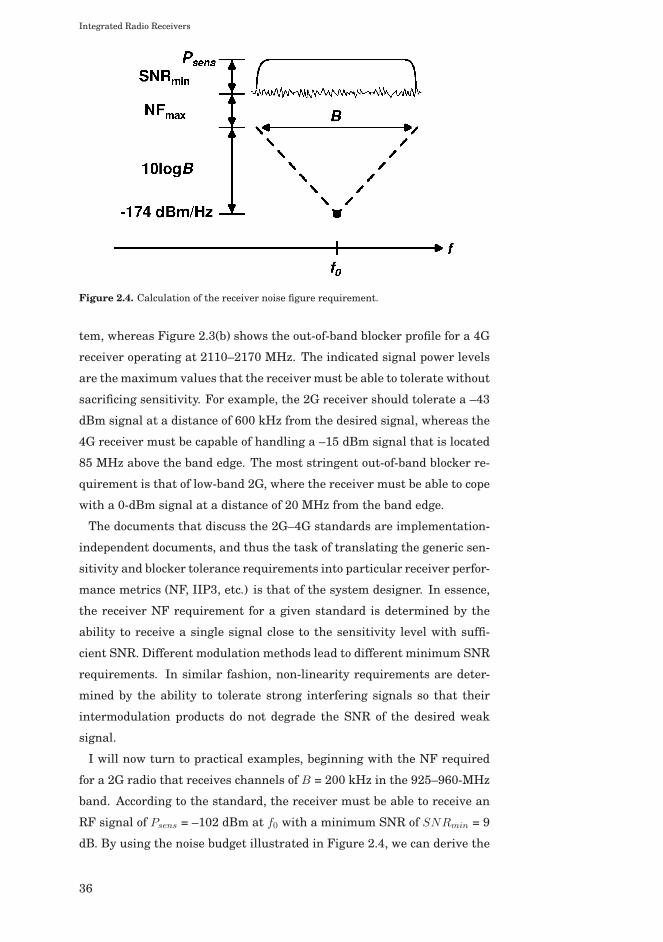
Figure 2.4. Calculation of the receiver noise figure requirement.
tem, whereas Figure 2.3(b) shows the out-of-band blocker profile for a 4G
receiver operating at 2110–2170 MHz. The indicated signal power levels
are the maximum values that the receiver must be able to tolerate without
sacrificing sensitivity. For example, the 2G receiver should tolerate a –43
dBm signal at a distance of 600 kHz from the desired signal, whereas the
4G receiver must be capable of handling a –15 dBm signal that is located
85 MHz above the band edge. The most stringent out-of-band blocker re-
quirement is that of low-band 2G, where the receiver must be able to cope
with a 0-dBm signal at a distance of 20 MHz from the band edge.
The documents that discuss the 2G–4G standards are implementation-
independent documents, and thus the task of translating the generic sen-
sitivity and blocker tolerance requirements into particular receiver perfor-
mance metrics (NF, IIP3, etc.) is that of the system designer. In essence,
the receiver NF requirement for a given standard is determined by the
ability to receive a single signal close to the sensitivity level with suffi-
cient SNR. Different modulation methods lead to different minimum SNR
requirements. In similar fashion, non-linearity requirements are deter-
mined by the ability to tolerate strong interfering signals so that their
intermodulation products do not degrade the SNR of the desired weak
signal.
I will now turn to practical examples, beginning with the NF required
for a 2G radio that receives channels of B = 200 kHz in the 925–960-MHz
band. According to the standard, the receiver must be able to receive an
RF signal of Psens = –102 dBm at f0 with a minimum SNR of SNRmin = 9
dB. By using the noise budget illustrated in Figure 2.4, we can derive the
36

Integrated Radio Receivers
Figure 2.5. Calculation of the LO phase noise requirement.
maximum allowed NF of the receiver and any preceding filters as
NFmax = Psens + 174dBm/Hz − 10logB − SNRmin ≈ 10dB. (2.13)
In practice, designers attempt to minimize the NF regardless of the speci-
fied NFmax, such that the receiver is able to operate with even lower Psens
values than required. Common targeted levels are 2–3 dB.
If we further consider the 0-dBm blocker that is 20 MHz away from the
band edge, we can derive a specification for the LO phase noise power, L,
at the 20-MHz offset to prevent NF degradation. Specifically, the LO-
dependent noise sideband of the downconverted blocker must be suffi-
ciently weak. The desired signal is in this case located in the final channel
at the band’s edge. This situation is illustrated as referred to RF in Figure
2.5, and we use the same values of B, Psens, and SNRmin as above:
L+ 10logB + Pblocker = Psens − SNRmin => L = −164dBc/Hz. (2.14)
In similar fashion, we obtain L = –121 dBc/Hz for a 600-kHz offset by
using Pblocker = –43 dBm, as discussed above. These requirements become
specifications for frequency synthesizer design.
IIP2 and IIP3 requirements are also standard-specific requirements,
and the interesting interferer offset frequencies are determined by the
use scenario. For example, one interesting IIP2 offset in FDD systems is
determined by the duplex distance to the co-existent transmitter, because
intermodulation of the leaked transmitter signal with itself in the receive
path is a major source of distortion. Likewise, one interesting out-of-band
IIP3 offset in an FDD system is determined by the duplex distance. In the
3G case of 1920–1980 MHz (TX) / 2110–2170 MHz (RX) discussed above,
37

Integrated Radio Receivers
the duplex distance is 190 MHz. A co-existent transmitter at the duplex
distance can produce an intermodulation product with a second interferer
that is placed in between the bands, in other words, at 95 MHz above the
receive frequency.
Furthermore, a particular in-band IIP3 test for 3G uses –46-dBm in-
terferer tones at 10 and 20 MHz offsets away from the receive frequency,
both of which represent other active 3G channels. The spread-spectrum-
based wideband code division multiple access (WCDMA) technology used
in 3G systems allows for negative values of SNRmin [48]. For example, for
a spreading and coding gain of 25 dB, an implementation margin of 2 dB,
and a bit energy to interference power ratio of 5 dB, we obtain SNRmin =
5 dB + 2 dB - 25 dB = –18 dB [49, p. 19]. The sensitivity level required
by the standard is –117 dBm, and by using a desired test signal of –114
dBm (3 dB above the sensitivity level), the allowed noise + intermodu-
lation product power is –114 dBm – (–18 dB) = –96 dBm. The required
in-band IIP3 can then be calculated by using equation (2.8) as follows:
IIP3 = −46dBm+−46dBm−−96dBm
2= −21dBm. (2.15)
For the out-of-band case, let us assume that the FDD TX transmits at
+32 dBm, which is sensed as –17 dBm at the receiver input after 45 dB of
duplexer isolation. We assume that a blocker is placed at one half that of
the duplex distance with a specified maximum power of –15 dBm. After
an assumed 30 dB of pre-select filtering, this blocker is sensed as –45
dBm at the receiver input [50, p. 22]. By using the same desired test
signal of –114 dBm and SNRmin as above, we again require the noise +
intermodulation product to be below –96 dBm. Hence, by using equation
(2.9) we obtain:
IIP3 =−17dBm
2− 45dBm− −96dBm
2= −5.5dBm. (2.16)
Designs usually require margins due to such reasons as fabrication and
temperature variations, and so higher IIP3 values would be targeted in
practice. More generally, if one considers a SAW-less future 2G/3G/4G
SDR that should tolerate its envisioned blocker environment, the work
in [51] suggests that an out-of-band IIP3 of +10-dBm is needed.
IIP2 requirements are set by similar considerations as those for IIP3.
Intermodulation due to the leakage of a co-existent transmitter signal into
the receiver chain of an FDD transceiver is a particular concern because
the frequency components of the leaked signal can intermodulate with
38
Integrated Radio Receivers
each other such that the products fall into the desired baseband channel.
Furthermore, in envisioned wideband receivers with little to no filtering,
strong RF blocker signals may intermodulate with each other such that
the products fall on top of a desired RF signal already in the LNA. De-
pending on the system and the filtering involved, the required IIP2 may
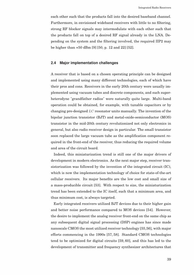
be higher than +50 dBm [9] [50, p. 12 and 22] [52].
2.4 Major implementation challenges
A receiver that is based on a chosen operating principle can be designed
and implemented using many different technologies, each of which have
their pros and cons. Receivers in the early 20th century were usually im-
plemented using vacuum tubes and discrete components, and such super-
heterodyne "grandfather radios" were naturally quite large. Multi-band
operation could be obtained, for example, with tunable capacitors or by
changing pre-designed LC resonator units manually. The invention of the
bipolar junction transistor (BJT) and metal-oxide-semiconductor (MOS)
transistor in the mid-20th century revolutionized not only electronics in
general, but also radio receiver design in particular. The small transistor
soon replaced the large vacuum tube as the amplification component re-
quired in the front-end of the receiver, thus reducing the required volume
and area of the circuit board.
Indeed, this miniaturization trend is still one of the major drivers of
development in modern electronics. As the next major step, receiver tran-
sistorization was followed by the invention of the integrated circuit (IC),
which is now the implementation technology of choice for state-of-the-art
cellular receivers. Its major benefits are the low cost and small size of
a mass-producible circuit [53]. With respect to size, the miniaturization
trend has been extended to the IC itself, such that a minimum area, and
thus minimum cost, is always targeted.
Early integrated receivers utilized BJT devices due to their higher gain
and better noise performance compared to MOS devices [54]. However,
the desire to implement the analog receiver front-end on the same chip as
any subsequent digital signal processing (DSP) engines has since made
nanoscale CMOS the most utilized receiver technology [55,56], with major
efforts commencing in the 1990s [57, 58]. Standard CMOS technologies
tend to be optimized for digital circuits [59, 60], and this has led to the
development of transmitter and frequency synthesizer architectures that
39

Integrated Radio Receivers
exploit this fact by being based on digital-intensive operation [61].
Receiver development has not followed this trend with equal speed, but
chapter 5 details experimental work in this direction. As a specific origi-
nal contribution of this dissertation, chapter 5 presents RF front-end mod-
eling and design for a direct delta-sigma receiver (DDSR) in 40-nm CMOS,
where signal discretization begins already at RF. The DDSR thus tran-
scends the conventional divide between the RF front-end and the subse-
quent A/D converter by assigning a digital-intensive role to the RF stages.
In turn, this requires a new front-end design methodology that accounts
for the new role.
As mentioned before, each implementation technology also has its prob-
lems. Using nanoscale CMOS for analog design in general requires ad-
dressing a number of non-idealities, such as limited signal headroom,
analog parameter variance, matching accuracy, and general device per-
formance [62]. Speaking specifically of the use of CMOS for RF receivers,
some of the major drawbacks are related to limited supply voltages, lim-
ited transistor linearity, and the limited quality of passive components
and consequent unavailability of high-Q resonators. I will now discuss
each of these briefly in light of the performance metrics and requirements
presented in the two previous sections.
Portable devices that contain an integrated receiver are mostly powered
by a re-chargeable battery. The battery is often based on Li-Ion technol-
ogy, with a nominal output voltage of 3.6–3.7 V and a variation between
3.0–4.2 V over a single charging cycle of the battery. In contrast, the sup-
ply voltage of core devices in modern CMOS technologies have decreased
from 3.3 V in 0.35-μm CMOS to 1.2 V in 65-nm CMOS and down to below
0.9 V in more advanced CMOS nodes [63]. This development is driven
mainly by advantages for digital circuitry. This means that a DC-DC con-
verter must be used to transform the battery voltage to a suitable level
for the CMOS devices. The converter consumes excess power depending
on its power efficiency, thus reducing the lifetime and subsequently the
autonomy of the portable device. Moreover, converters with a higher effi-
ciency are usually external and thus increase the size of the system sub-
stantially. I discuss efforts to integrate this function in chapter 4, which
focuses on buck-type converters and on my original work in 65-nm CMOS
on a fully integrated 3.6-to-1.8-V cascode converter design.
The full integration of a switched-mode DC-DC converter also ties to the
more generic issue of the spectral purity of signals. This issue is tradition-
40

Integrated Radio Receivers
ally considered in relation to integrated PLLs that generate RF local oscil-
lator signals. Unfortunately, circuit imperfections cause these LO signals
to exhibit spurious tones, located at offsets that are multiples of the used
reference oscillator frequency. This phenomenon can lead to challenging
problems when the PLL is used in multi-channel systems, particularly in
submicron CMOS, and various spurious tone reduction techniques have
been proposed [64]. One of these is proper frequency planning, and this
technique may also be useful when designing fully integrated DC-DC con-
verters for transceiver applications. Their periodic output voltage ripple
couples to the RF circuitry that they supply [65], and similar to spurious
clock tones from a PLL, the spectral content of the ripple may lead to un-
desired signal mixing. The use of a very high switching frequency, as in
the work presented in chapter 4, can mitigate this problem.
The reduced supply voltage of submicron CMOS technologies leads to
decreased headroom for analog signals, that is, to limited voltage swings
and a limited dynamic range for the receiver. In turn, this leads to ma-
jor problems due to strong interfering signals that, once amplified, can
overload the receiver and thus corrupt the reception of a weak desired
signal. This effect is also closely related to the inherent non-linearity of
the amplification devices, that is, the MOS transistors [66]. Compressive
non-linearity is preceded by small-signal non-linearity, where two weaker
interfering signals may still produce intermodulation products that cor-
rupt the desired signal. In particular, the transconductance (gm) and out-
put conductance (gds) of the MOS transistor in low-VDD nanoscale CMOS
technologies are the fundamental sources of non-linear behavior [67] in
design approaches that rely on voltage-mode design. For second-order
non-linearity in particular, effects such as RF signal self-mixing and chip-
to-chip variations in the form of mixer device mismatches also play an
important role [42].
Passive components tend to exhibit very good linearity in comparison to
MOS devices. Their major drawbacks lie in fabrication value tolerances,
and for reactive components in particular, in their small achievable size
and poor quality factor, Q. For example, capacitance values may exhibit
a spread of 20% once fabricated, whereas capacitor and inductor sizes are
limited to the low nF/nH range. This prevents the integration of low-
frequency LC BPFs, whereas the low Q of bulk CMOS inductors (gen-
erally < 20) prevents the integration of low-noise and high-Q LC BPFs
at high frequencies. This is a major reason that has so far prevented
41
Integrated Radio Receivers
the monolithic integration of the pre-select filter and the integration of
an external image-reject filter in a superheterodyne receiver. The toler-
ance problem can be reduced by using design techniques that rely on rela-
tive ratios instead of absolute values, and by using electronic tuning tech-
niques to center low-Q LC resonators at the desired frequency. Chapter
3 covers my related original work on two experimental circuits, namely a
2.1-GHz VCO in 0.25-μm BiCMOS and a 2.5-GHz RF front-end. The first
circuit looks at high-Q resonator integration through device technology,
whereas the latter focuses on exploiting a useful circuit technique.
42

3. High-Q Component Integration
3.1 Overview
Receivers require a number of building blocks that filter signals and cre-
ate accurate frequency references. The former function enables a receiver
to operate in an interference-rich environment, whereas the latter en-
sures that a clean oscillator signal can be generated and the correct in-
put signal can be received. Both of these functions require components
with high quality factors (Q), which translates to sharp resonances or
impedance responses. Because of integration difficulties, these compo-
nents are usually external to the IC and thus increase the area required
for receiver implementation.
In this chapter, my contributions focus specifically on bandpass filtering
and on the reference oscillator in the frequency synthesizer. After first
reviewing the context, the chapter highlights some of the most significant
parts of the original work. Further details on analysis and implementa-
tion are presented in the related scientific publications [I], [II], and [VII].
From a physical standpoint, Q quantifies the ability of an electronic com-
ponent to store energy versus energy losses. For example, inductors store
energy in a magnetic field, whereas capacitors store energy in an electric
field, but some of the energy is lost due to leakage. Accordingly, [68, p. 89]
explains that Q can also be expressed as the ratio of stored energy and
lost energy per unit time. For these components, Q at a given frequency
can be defined as
Q =|Im(Z)|Re(Z)
=|X|R
, (3.1)
where Z is the impedance of the component, and X and R are respectively
the reactance and resistance of impedance Z. The maximum Q of spiral
inductors in modern CMOS technologies is usually below 20, whereas in-
43

High-Q Component Integration
tegrated capacitors tend to perform much better even at GHz-range fre-
quencies. The inductor is therefore usually the bottleneck for achieving a
good Q and thus high selectivity for an LC resonator, because
1
QLC=
1
QL+
1
QC. (3.2)
The selectivity perspective is most important in terms of this disser-
tation, and thus the most useful definition for Q is tied to the center
frequency, f0, and the –3-dB bandwidth, B, of the response, such that
Q = f0/B. In other words, a sharp bandpass response requires a low
value of B and thus a high value of Q. As an example, if we assume that
QLC = 10 and f0 = 2 GHz, we obtain B = 200 MHz. This is far too high
for implementing the kind of out-of-band pre-select filtering required by
the systems discussed in chapter 2, even if several LC resonators were
connected together to form more complicated filters. The same conclusion
holds true for frequency synthesizers, where the reference oscillator must
be very accurate and stable. A QLC of 10 cannot be used to achieve suffi-
cient frequency stability, nor are the fabrication tolerances of integrated
LC resonators such that their center frequency is sufficiently accurate
and repeatable for this purpose.
As a consequence, integrated radio receivers use pre-select filters and/or
duplexers that are based on surface acoustic wave (SAW) or bulk acoustic
wave (BAW) technology. Although their performance is good, they con-
sume space and complicate the manufacturing process. Furthermore, be-
cause they are mechanical structures their operating frequencies are not
easily tunable, which in turn leads to the requirement for multiple paral-
lel signal paths in a multi-standard receiver. Likewise, receivers use an
off-chip quartz crystal as a resonator, which makes it possible to design
a reference oscillator with sufficient accuracy and stability [69]. These
crystals also offer very limited frequency tuning possibilities.
The design community is currently searching for integrable alternatives
to these off-chip components. The search can be divided into new types of
components and new types of circuit techniques. The remainder of this
chapter discusses two alternatives. First, I present the above-IC integra-
tion of a BAW resonator for use in a 2.1-GHz VCO, where the target is to
achieve very good phase noise performance without completely sacrificing
the frequency tuning range. I then discuss N-path filtering, which is a re-
cently re-discovered circuit technique that is being investigated in terms
of pre-select filter replacement in receivers. I use a programmable N-path
44

High-Q Component Integration
Figure 3.1. Physical structure of (a) an FBAR and (b) an SMR.
filter in a 2.5-GHz receiver front-end in order to boost the blocker filtering
done by the LNA.
3.2 Bulk Acoustic Wave resonators
Bulk Acoustic Wave (BAW) resonators belong to the family of microelec-
tromechanical system (MEMS) components. They can be used, for ex-
ample, in multi-stage filters or in an oscillator, as in publications [I] and
[II] of this dissertation. These resonators utilize the piezoelectric effect,
meaning that electrical energy sensed by the resonator is converted into
mechanical energy (in this case, acoustic energy) at its input electrode
and vice versa at the output electrode. The word "bulk" denotes that the
acoustic energy is transferred from input to output within the body of the
component rather than on its surface, which is the case in Surface Acous-
tic Wave (SAW) resonators. The bulk consists of a thin film of piezoelec-
tric material, for example aluminum nitride (AlN), that has been grown
between the input and output electrodes.
BAW resonators can be further divided into film bulk acoustic resonators
(FBAR) and solidly mounted resonators (SMR), shown in Figure 3.1 [70,
71]. They differ in their physical structure, particularly in the manner in
which one of the electrodes is isolated acoustically from the substrate [72].
The resonators are often grown on their own substrates, after which they
are connected to other IC devices using bondwires [73] or with flip-chip
technology [74, 75]. Another more complicated option is to grow the res-
onator above an otherwise ready IC, which gives rise to the term "above-
IC" resonator [11,70,76]. This approach is attractive in terms of integra-
tion, because it saves circuit area and avoids the parasitic effects of the
bondwires. Although the result is not a conventional monolithic IC, the
post-processing directly on top of the active circuitry produces a quasi-
monolithic chip that can be regarded as quite similar to a conventional
IC.
45
High-Q Component Integration
The electrical behavior of the BAW resonator resembles that of a quartz
resonator, with the benefit that it operates at higher frequencies (100 MHz
to at least 5 GHz), with at least partial integrability, and is smaller (for
example, 300 x 300 μm2). The impedance response exhibits first a series
resonance frequency (fs) and later a parallel resonance (fp), along with
their attenuated harmonic overtones. The separation between fs and fp
is determined by the electromechanical coupling coefficient, k2t :
k2t =π2
8
f2p − f2
s
f2p
≈ π2
8
Cm
C0, (3.3)
where Cm and C0 refer to lumped-element model components that will
be discussed shortly. The value of k2t in BAW resonators is usually low
(on the order of 0.02–0.1) [77]. The resonances at fs and fp thus lie very
close to each other, for example at a distance of 60 MHz for a 2.1-GHz
resonator, which limits the external tunability of the resonator and thus
its usable frequency range. This is a problem in view of the required
receiver flexibility [78], but it can also be seen as a benefit in view of
frequency accuracy. Specific work aimed at the intrinsic and extrinsic
frequency tuning of BAW resonators has reached a tuning range of only a
few percentage points [79], with associated tradeoffs.
The main attraction of the BAW resonator is that the Q of the reso-
nances is easily higher than 500. This is much lower than for a non-
integrable quartz crystal (often in the tens of thousands), but significantly
higher than can be achieved with monolithic LC resonators (typically up
to 20) in modern BiCMOS and CMOS technologies. Moreover, they are
linear and tolerate very high input signal powers, and in contrast to SAW
resonators, they can, to a certain degree, be integrated [30].
During circuit design, the BAW resonator is modeled using a lumped-
element equivalent circuit that is extracted during separate BAW pro-
cessing and characterization steps. Variants of the model are shown in
Figure 3.2, where the Butterworth-Van Dyke (BVD) model is the one tra-
ditionally used for quartz crystal resonators. Figure 3.2(b) and (c) show
developments of this model that aim to capture the specific properties of
the BAW resonator, with the Modified BVD (MBVD) model [80] being a
useful approximation of the Generalized BVD (GBVD) model [81] for low-
k2t cases. Bondwire and I/O pad models should be added to these models
in a non-above-IC case.
The series resonance branch is formed by the motional impedances Lm,
Cm, and Rm. Parallel resonance is realized by adding electrode plate ca-
46

High-Q Component Integration
Figure 3.2. Models of the FBAR: (a) Butterworth-Van Dyke, (b) Modified Butterworth-Van Dyke, and (c) Generalized Butterworth-Van Dyke.
Figure 3.3. Impedance response of a typical FBAR, with MBVD model element valuesfrom the resonator employed in publication [I].
47

High-Q Component Integration
pacitance C0, whereas R0 and Rser represent losses due to the plate and
external connection resistances, respectively. A sample FBAR impedance
response is plotted in Figure 3.3. It uses the MBVD model values that
describe the resonator used in our original work in publication [I], with a
series resonance at fs = 2.151 GHz and a parallel resonance at fp = 2.207
GHz. The response resembles that of a quartz resonator, although it is at
a much higher frequency and with less pronounced resonances due to a
lower Q. The MBVD model can be used to define the resonance frequen-
cies as follows:
fs =1
2π√LmCm
, (3.4)
fp =1
2π√
LmC0Cm
C0+Cm
= fs
√1 +
Cm
C0. (3.5)
BAW resonator properties imply that it can successfully be used as a
stand-alone resonator in oscillators and as a building block for more com-
plicated lattice, ladder, or stacked crystal structures used for bandpass
filtering [82, 83]. The resonators have been mass produced commercially
in duplex filters since the early 2000s, thus replacing old ceramic struc-
tures [84, 85]. Recent efforts at further resonator improvement have fo-
cused on improving their frequency accuracy and temperature stability,
which is important for potential oscillator use [77,86]. The frequency can
then be fine-tuned using parallel capacitor banks [87].
The use of BAW resonators in voltage-controlled oscillators (VCO) is still
an experimental technique. The envisioned applications include usage as
an RF VCO in a phase-locked loop (PLL) that requires a low-frequency
silicon-integrable reference [88], or in a quartz-less receiver without the
need for a PLL [89–91]. These examples have been demonstrated for the
2.4-GHz band. To the best of the author’s knowledge, there are as of yet
no cellular receiver demonstrators, and the potential application field is
not discussed further here.
With respect to oscillator architecture, the common-base [74], modified
cross-coupled [92–94], Colpitts [89, 95], and Pierce [96–99] architectures
are some of the typical choices. The high value of Q enables both low phase
noise and very low power consumption when required. The original work
in this dissertation applies the BAW resonator to a Butler-based VCO in
publications [I] and [II], with highlights provided in chapter 3.4.2.
48
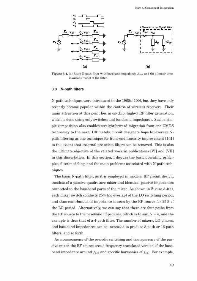
High-Q Component Integration
Figure 3.4. (a) Basic N-path filter with baseband impedance ZBB and (b) a linear time-invariant model of the filter.
3.3 N-path filters
N-path techniques were introduced in the 1960s [100], but they have only
recently become popular within the context of wireless receivers. Their
main attraction at this point lies in on-chip, high-Q RF filter generation,
which is done using only switches and baseband impedances. Such a sim-
ple composition also enables straightforward migration from one CMOS
technology to the next. Ultimately, circuit designers hope to leverage N-
path filtering as one technique for front-end linearity improvement [101]
to the extent that external pre-select filters can be removed. This is also
the ultimate objective of the related work in publications [VI] and [VII]
in this dissertation. In this section, I discuss the basic operating princi-
ples, filter modeling, and the main problems associated with N-path tech-
niques.
The basic N-path filter, as it is employed in modern RF circuit design,
consists of a passive quadrature mixer and identical passive impedances
connected to the baseband ports of the mixer. As shown in Figure 3.4(a),
each mixer switch conducts 25% (no overlap) of the LO switching period,
and thus each baseband impedance is seen by the RF source for 25% of
the LO period. Alternatively, we can say that there are four paths from
the RF source to the baseband impedance, which is to say, N = 4, and the
example is thus that of a 4-path filter. The number of mixers, LO phases,
and baseband impedances can be increased to produce 8-path or 16-path
filters, and so forth.
As a consequence of the periodic switching and transparency of the pas-
sive mixer, the RF source sees a frequency-translated version of the base-
band impedance around fLO and specific harmonics of fLO. For example,
49

High-Q Component Integration
whereas the impedance of a baseband capacitor can be thought of as a
bandpass function around DC, it is seen at the RF side as a bandpass func-
tion around fLO (and specific harmonics). The Q of the resulting bandpass
filter depends only on the size of the capacitor, not for example on the LO
frequency being used. In addition to being easy to integrate, such relative
frequency-independence is a highly attractive feature of the N-path filter.
Interestingly, the loading effect or input impedance of the N-path filter
depends on the RF source impedance that drives it, even at fLO, where the
capacitors themselves would be seen at the RF port as infinite impedances
(which they are at DC). This property results from the transparent nature
of the passive mixer. Specifically, while our main focus usually is on op-
eration around fLO, it should be kept in mind that the rectangular LO
signal of 25-% duty cycle also has content at harmonics of fLO. Because of
this, the downconverted voltage at the baseband nodes is re-upconverted
to those harmonics, resulting in power dissipation in the mixer switches
and the RF source impedance. Because of charge conservation and bal-
ance, the RF signal must supply the charge dissipated as a result of the
re-upconversion of the signal. This results in a non-zero charge flow from
RF to the baseband side also at fLO, which corresponds to a finite input
impedance.
Effective modeling is very useful for understanding and employing the
N-path filter as part of a larger design, especially since it is a linear peri-
odically time-variant (LPTV) arrangement. Preferably, the model should
be sophisticated enough to capture the main behavioral and non-ideal
properties of the filter, but simple enough to enable straightforward anal-
ysis and an intuitive understanding of how different components affect
filter behavior. Several models have recently been proposed. For exam-
ple, the study in [102] focuses on resistive source impedances and pro-
poses a full LPTV model that can be reduced to an equivalent RLC circuit
around fLO, whereas two other studies [103] and [104] look at practically
arbitrary source impedances and propose full mathematical LPTV models
that capture filter behavior throughout the frequency range.
The derivation in [105] is also based on LPTV analysis, but simplifica-
tion around fLO produced a useful lumped-element, linear time-invariant
(LTI) equivalent circuit. As shown in Figure 3.4(b), the model consists of
an RF source impedance, Zs, a mixer switch resistance, RSW , a baseband
impedance ZBB, and a virtual shunt impedance, Zsh. The scaling factor γ
reflects ZBB correctly at the RF port, and Zsh accounts for the effects due
50
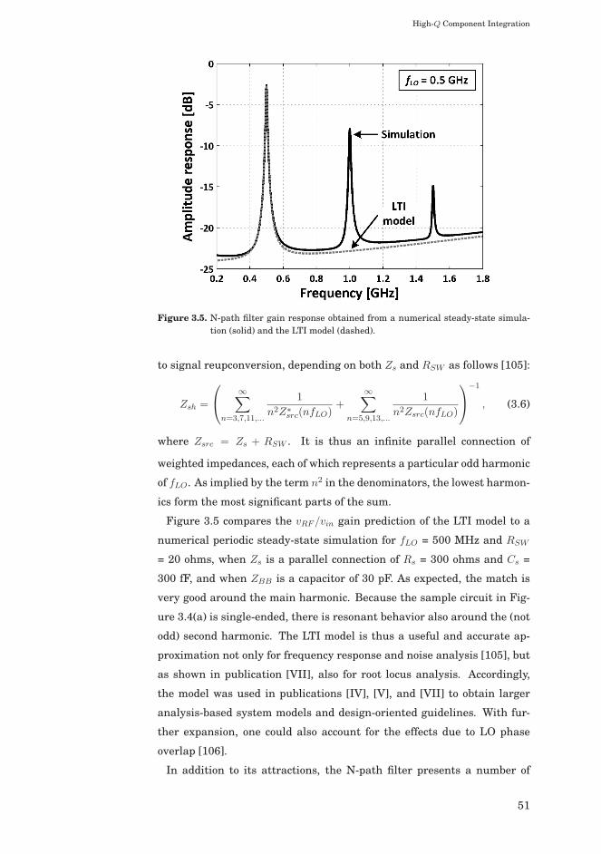
High-Q Component Integration
Figure 3.5. N-path filter gain response obtained from a numerical steady-state simula-tion (solid) and the LTI model (dashed).
to signal reupconversion, depending on both Zs and RSW as follows [105]:
Zsh =
⎛⎝ ∞∑
n=3,7,11,...
1
n2Z∗src(nfLO)+
∞∑n=5,9,13,...
1
n2Zsrc(nfLO)
⎞⎠−1
, (3.6)
where Zsrc = Zs + RSW . It is thus an infinite parallel connection of
weighted impedances, each of which represents a particular odd harmonic
of fLO. As implied by the term n2 in the denominators, the lowest harmon-
ics form the most significant parts of the sum.
Figure 3.5 compares the vRF /vin gain prediction of the LTI model to a
numerical periodic steady-state simulation for fLO = 500 MHz and RSW
= 20 ohms, when Zs is a parallel connection of Rs = 300 ohms and Cs =
300 fF, and when ZBB is a capacitor of 30 pF. As expected, the match is
very good around the main harmonic. Because the sample circuit in Fig-
ure 3.4(a) is single-ended, there is resonant behavior also around the (not
odd) second harmonic. The LTI model is thus a useful and accurate ap-
proximation not only for frequency response and noise analysis [105], but
as shown in publication [VII], also for root locus analysis. Accordingly,
the model was used in publications [IV], [V], and [VII] to obtain larger
analysis-based system models and design-oriented guidelines. With fur-
ther expansion, one could also account for the effects due to LO phase
overlap [106].
In addition to its attractions, the N-path filter presents a number of
51

High-Q Component Integration
problems that have so far prevented its widespread employment. Many
of these problems are also shown in Figure 3.5. First, the filter has lim-
ited selectivity at far-away offsets due to passive mixer switch resistance,
which poses a problem in terms of SAW filter replacement. The simplest
approaches for increasing the selectivity are to increase the RF source
impedance and reduce the switch resistance, but both have practical lim-
its. Instead, another study [107] proposes the use of a second mixer to
reupconvert the filtered baseband signal, thus removing the effect of the
mixer switches. This bandpass filter suffered from high noise, but further
developments proposed in a follow-up study [108] solved that problem by
using active circuitry while still maintaining high linearity.
Second, the rectangular LO signal for the passive mixer has content
at the harmonics of fLO, as discussed previously. The response at even
harmonics can be suppressed by using balanced circuitry. As a result of
the harmonic response, signals around the odd harmonics that start with
(N − 1)fLO, where N is the number of LO phases, will fold on top of the
desired signal and can no longer be separated from it at baseband. Using
a higher number of LO phases (for example 8 or 16) alleviates the prob-
lem, at the expense of a more complicated design. For example, 8-phase
switching can be used in the LTE frequency range 0.7–2.7 GHz, where the
lowest harmonic content to fold would be outside the LTE band at 7 x 0.7
GHz = 4.9 GHz, but the 5-GHz wireless local area network (WLAN) band
still poses a problem. Receivers using 8-path filtering typically employ
weighted harmonic-rejection mixing [109] and recombination amplifiers,
in which baseband signals from the different mixing paths are summed
such that the effective LO signal is a sinusoid at fLO. If the paths are
weighted properly, this cancels out the harmonic content [110–113]. Fur-
ther techniques have been proposed to cancel out the compressive effect
of blockers at the harmonics of fLO [114], but it is still unclear whether
sufficient harmonic rejection can be achieved.
In addition to these two main problems, N-path filters require an LO
signal with very low phase noise to reduce reciprocal mixing. They also
exhibit potential LO leakage to the antenna interface (up to –60 dBm
depending on their placement [115]); a MHz-class frequency offset from
a GHz-range fLO, and consequently an unsymmetric bandpass response
when using non-resistive source impedances; and they consume LO drive
power (as opposed to the passive SAW filter).
Nevertheless, N-path-based circuits remain an interesting and promis-
52

High-Q Component Integration
ing topic of research for highly linear and programmable receivers. The
filtering can be done in parallel to an RF node, or it can be combined
with the downconversion mixing so that the desired signal is processed
further at baseband. To give a few examples, N-path techniques have
thus far been used to implement passive-mixer-first receivers [35, 110–
113, 116], direct delta-sigma receivers with active front-ends [117] [VI],
analog front-ends [118–120], including structures with feedback [121,122]
and feedforward [123] blocker filtering, bandpass filters [102, 107, 108],
and notch filters [124].
In this dissertation, N-path filtering has been used in both a direct delta-
sigma receiver in publications [IV], [V], and [VI] and in an analog RF
front-end in publication [VII]. Highlights of the original work are pro-
vided in chapter 5 and section 3.4.1, and details are provided in the listed
scientific publications.
3.4 Experimental work
As original work for this dissertation, the two high-Q resonator tech-
niques discussed above were both embedded in separate experimental
ICs. I will first provide an overview of the implementation and measure-
ments of an RF front-end with N-path filtering, after which I will do the
same for a VCO that utilizes an above-IC FBAR as the main frequency-
setting element. Further analytical and technical details are covered in
the related publications.
3.4.1 Receiver front-end
As detailed in publication [VII] and as depicted in Figure 3.6, an N-path
filter was implemented in parallel to an LC resonator in a narrowband
2.5-GHz LNA load, thus improving the degree of available RF filtering in
the experimental receiver front-end. The same LNA structure, based on
an inductively degenerated common-source amplifier, was used in the nar-
rowband reference direct delta-sigma receiver design discussed in publi-
cation [VI] and another study [125]. The LNA was followed by a boosted
source-follower buffer (Gm) and passive I/Q downconversion mixing, after
which the signal was processed using low-pass transimpedance amplifiers
(TIA) with a bandwidth of approximately 10 MHz. The circuit was fabri-
cated in 40-nm CMOS and supplied by VDD = 1.1 V.
53

High-Q Component Integration
Figure 3.6. Block diagram of the experimental 2.5-GHz receiver front-end [VII]. ©2014IEEE.
Figure 3.7. LNA output interface in the 2.5-GHz receiver front-end, including the place-ment of the N-path filter.
54

High-Q Component Integration
The LNA output interface in Figure 3.7 was enhanced further by adding
a 3-bit programmable negative conductance circuit, –G, in parallel to the
LC and N-path resonators. This boosted the action of the LC and N-path
filters through increased resonator Q [126, 127]. The programmability
was implemented by connecting three binary-weighted switchable cells
of cross-coupled NMOS devices in parallel. These devices are all resis-
tively degenerated; Q-enhancement circuits close to the RF input other-
wise tend to severely limit the achievable linearity. The LC load is also
programmable so that it can be made to resonate at fLO = 2.5 GHz, which
in turn will result in the best N-path resonator response.
Based on our analysis in publication [VII], the loaded voltage gain of the
LNA can be derived as
Av,LNA =2gm,LNAZRLC(2γ(RSW + Zsh) + sIFRSWZshCNpath)
2γ(ZRLC +RSW + Zsh) + sIFCNpathZsh(ZRLC +RSW ), (3.7)
where gm,LNA is the equivalent transconductance of the LNA, ZRLC is the
total impedance of the load circuit composed of –G, L, C, and Ctune, and
sIF = j(ω−ωLO) is the distance from the LO frequency, ωLO = 2πfLO. Nor-
mally, minimizing the passive mixer switch resistance RSW in the N-path
filter will lead to the best blocker attenuation. However, the original work
presented in publication [VII] demonstrated that when driven by circuits
with internal LC loads, the N-path filter behaves counter-intuitively. As
illustrated in Figure 3.8 for design values that are in the general range of
our implementation, minimum passive mixer switch resistance does not
provide the best relative (Av,LNA(fLO)−Av,LNA(fblocker)) blocker attenua-
tion. Rather, there is a case-specific optimum value for the resistance, in
this case about 40–50 Ω. The design-oriented analysis provided in publica-
tion [VII] further shows that minimum switch resistance does not provide
a minimum front-end noise figure.
Figure 3.9 shows the implementation of the N-path filter, based on four
NMOS switches (40 μm/0.11 μm) and 20-pF baseband capacitors. The
source terminals of the switches were biased to the circuit’s common-mode
voltage, VCM = 0.55 V. The rail-to-rail LO pulses at the device gates re-
sulted in RSW = 27Ω. The size of the baseband capacitor was a tradeoff
between the 3-dB bandwidth of the resulting filtering response and the
chip area required to implement the capacitors.
In this particular front-end architecture, the N-path filter was in paral-
lel to the LNA load and thus separated from the downconversion mixing
function. It was thus possible to isolate the effect of the N-path filter-
55
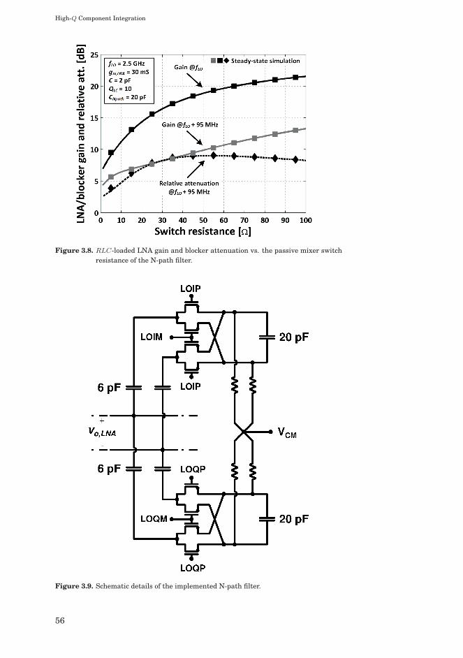
High-Q Component Integration
Figure 3.8. RLC-loaded LNA gain and blocker attenuation vs. the passive mixer switchresistance of the N-path filter.
Figure 3.9. Schematic details of the implemented N-path filter.
56
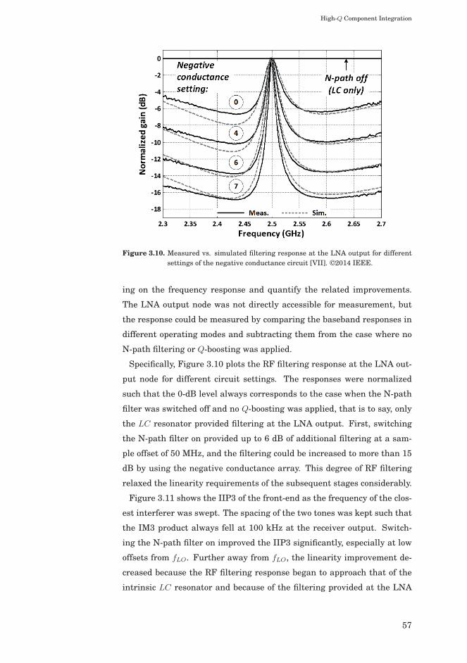
High-Q Component Integration
Figure 3.10. Measured vs. simulated filtering response at the LNA output for differentsettings of the negative conductance circuit [VII]. ©2014 IEEE.
ing on the frequency response and quantify the related improvements.
The LNA output node was not directly accessible for measurement, but
the response could be measured by comparing the baseband responses in
different operating modes and subtracting them from the case where no
N-path filtering or Q-boosting was applied.
Specifically, Figure 3.10 plots the RF filtering response at the LNA out-
put node for different circuit settings. The responses were normalized
such that the 0-dB level always corresponds to the case when the N-path
filter was switched off and no Q-boosting was applied, that is to say, only
the LC resonator provided filtering at the LNA output. First, switching
the N-path filter on provided up to 6 dB of additional filtering at a sam-
ple offset of 50 MHz, and the filtering could be increased to more than 15
dB by using the negative conductance array. This degree of RF filtering
relaxed the linearity requirements of the subsequent stages considerably.
Figure 3.11 shows the IIP3 of the front-end as the frequency of the clos-
est interferer was swept. The spacing of the two tones was kept such that
the IM3 product always fell at 100 kHz at the receiver output. Switch-
ing the N-path filter on improved the IIP3 significantly, especially at low
offsets from fLO. Further away from fLO, the linearity improvement de-
creased because the RF filtering response began to approach that of the
intrinsic LC resonator and because of the filtering provided at the LNA
57

High-Q Component Integration
Figure 3.11. Measured vs. simulated receiver IIP3 around fLO = 2.5 GHz [VII]. ©2014IEEE.
input by the frequency-selective input matching circuitry. Use of the neg-
ative conductance circuit had very little effect on the linearity.
It should be noted that these improvements in RF filtering and linearity
came at some cost to other performance. For example, the use of negative
conductance can increase the in-band gain of the front-end by more than
10 dB, depending on the 3-bit setting. This can be counteracted by reduc-
ing the gain of the post-LNA downconversion stage, resulting in a higher
NF in such situations. Moreover, each 3-bit tuning step is associated with
a 1.8-mA increase in current consumption, whereas the N-path filtering
incurs a constant current penalty of 8 mA due to the LO drive circuitry.
These tradeoffs must be assessed based on the requirements imposed by
momentary operating conditions. At times, the presence of strong inter-
fering signals may require the costly use of stronger filtering, whereas the
programmability of the circuit can be leveraged by reducing the filtering
and the attendant power consumption in quieter conditions.
Table 3.1 lists the performance of the 2.5-GHz receiver front-end. In
summary, the N-path filtering at the LNA output boosted the operation
of the LC resonator significantly. It improved the out-of-band IIP3 sig-
nificantly, and the relative filtering of blockers could be enhanced further
by using negative conductance for Q-boosting. In contrast to conventional
thinking, our analysis showed that an N-path filter with minimum switch
58

High-Q Component Integration
Parameter Value
fLO [GHz] 2.5
Gain [dB] 38.7
NF [dB] 3.5
OB-IIP3 [dBm] +3
IIP2 [dBm] +46
B–1dBCP [dBm] –14
VDD [V] 1.1
Power [mW] 53
Active area [mm2] 0.75
CMOS technology [nm] 40
Table 3.1. Performance summary of the 2.5-GHz receiver front-end (for OB-IIP3, IIP2,and B–1dBCP, the closest interferer is at fLO + 95 MHz).
resistance provides neither the best relative blocker filtering nor the low-
est noise figure. Further details on the analysis, a proposed input match-
ing method, the implementation, and measurements of the front-end are
provided in publication [VII].
3.4.2 FBAR oscillator
As a related original contribution of this dissertation, a high-Q FBAR was
integrated as part of a VCO in 0.25-μm SiGe:C BiCMOS. The main objec-
tive was to compare the performance of LC and FBAR-based implementa-
tions and to see whether an FBAR-based implementation could be made
reliably. The targeted frequency range was the WCDMA user equipment’s
receive band at 2.11–2.17 GHz, and the supply voltage VCC = 2.4 V.
A schematic of the oscillator is shown in Figure 3.12. It is a further de-
velopment of the Butler oscillator architecture and the architecture pre-
sented in reference [128], with the core consisting of a common-base/com-
mon-collector (CB/CC) amplifier loop. This loop exhibits positive feedback
and leads to oscillation, where the frequency is determined partly by the
parallel LC resonator loading of the CB stage and partly by the second
resonator connected in series as part of the feedback path. As depicted in
Figure 3.12, this second resonator was implemented either as a series LC
connection or as an above-IC FBAR through post-processing steps. The
parallel LC resonator is not required, but it improves the spectral purity
of the VCO and provides more voltage headroom for the CB stage.
59

High-Q Component Integration
Figure 3.12. Schematic of the implemented LC/FBAR-based voltage-controlled oscillator.
The frequency tuning is based on changing the bias point and input
impedance of the CB stage. Changes in the bias current are reflected
in the voltage over R3, and in the fully-LC implementation, thus in the
voltage over the NMOS series varactor, Ctune. The oscillation frequency
changes as a consequence of the changes in the LC resonance frequency.
The FBAR implementation did not include a varactor, and as analyzed in
publication [I], the frequency tuning is now based on three factors. First,
the input impedance of the CB stage around Q1 decreases together with
VCTRL. Second, the input impedance of the CC stage around Q2 depends
on its load, which is in part the input impedance of the CB stage. Changes
in the latter at high VCTRL values lead to the real part of the former be-
coming negative. Third, the grounding capacitor, C1, creates an imperfect
short circuit in the low-GHz range. Taken together, these factors alter the
loop gain response such that the oscillation frequency changes.
A total of four oscillator versions were designed: a single-ended refer-
ence LC oscillator, a single-ended FBAR oscillator, a single-ended FBAR
oscillator with conversion to a differential output signal, and an FBAR
oscillator that was integrated with an experimental WCDMA front-end,
which is discussed in another study [12, pp. 228–231]. Here, I focus on
the first three versions. The best phase noise of the reference LC VCO
and the differential-output FBAR VCO are compared in Figure 3.13. The
latter achieved a best value of –143.7 dBc/Hz at an offset of 1 MHz from
the carrier. The single-ended FBAR VCO demonstrated similar low-offset
performance, but the high-offset noise was about 2 dB lower, most likely
due to the simpler output buffering. The reference LC VCO had a best
value of –126.0 dBc/Hz at the 1-MHz offset. A considerable improvement
in frequency stability was thus observed when using the high-Q FBAR.
60

High-Q Component Integration
Figure 3.13. Comparison of LC vs. FBAR VCO phase noise at optimum conditions [I].©2006 IEEE.
Parameter SE FBAR Diff. FBAR LC
Tuning range [MHz] 37 15 128
Best phase noise @1 MHz
offset [dBc/Hz]
–144.1 –143.7 –126.0
Best phase noise @3 MHz
offset [dBc/Hz]
–149.6 –147.3 –135.0
Output power @50Ω [dBm] –13..–2.5 –15..–6.5 –12..-1.7
VCC [V] 2.4
Current consumption [mA] 11–30 22–39 11–26
BiCMOS technology [μm] 0.25
Table 3.2. Performance summary of the 2.1-GHz voltage-controlled oscillators.
Although the phase noise changed as a function of VCTRL, the frequency
stability improved throughout.
The single-ended FBAR VCO had a modest frequency tuning range of
37 MHz (from 2.061 to 2.098 GHz). To the best of the author’s knowl-
edge, this was the largest tuning range reported for an FBAR VCO at the
time the results were published. Subsequently, it appears to have been
superceded only by an oscillator in [93]. It should be noted that the oscil-
lation frequency is shifted from the WCDMA band. In this connection, an
important part of subsequent FBAR-related research has focused on the
frequency accuracy of the FBAR and the ability to merely fine-tune the
frequency around a given reference frequency [77, 87]. Table 3.2 summa-
61

High-Q Component Integration
rizes the performance of the three VCO versions.
Above-IC technology in particular presents another challenge, namely
the yield in properly connecting the IC and the above-IC parts to each
other. The related electrode contact resistance should normally be very
low (on the order of 1 Ω or less), but defects may occur that result in
significant increases. To obtain a further qualitative and quantitative un-
derstanding of this topic, publication [II] analyzes the effects on this par-
ticular FBAR VCO topology, asking "How severe can the manufacturing
effects be for the circuit to still oscillate?"
This question can be answered at least in part by performing extensive
time-domain simulations, with for example the frequency control voltage
VCTRL and the FBAR Rser (and thus the series resonance quality factor
Qs) used as parameters. However, such an approach is ineffective and
time-consuming. Instead, the original work presented in publication [II]
uses root locus analysis to mathematically determine the limits of oscilla-
tion for all possible combinations of the two, starting from a design with
otherwise set component values. As shown in Figure 3.14, the VCO ex-
hibits two roots in the right-hand plane (RHP) that are responsible for
oscillation when VCTRL rises above 0.76 V. One of them (λ0) is located
close to the imaginary axis of the s-plane, indicating high-Q behavior and
a slower start-up. Based on transient simulation, this lower-frequency
root eventually takes over and determines the oscillation frequency. Be-
cause both Qs and VCTRL affect the VCO’s start-up, a full solution to the
problem requires an examination of the RHP crossing point of λ0 for all
combinations of Qs and VCTRL.
The result is shown in Figure 3.15 and is divided into regions of suc-
cessful and unsuccessful start-up on f0. Each point of the upper dividing
line corresponds to the value of VCTRL (for a given value of Qs) at which
λ0 crosses the imaginary axis. For analytical purposes, the region of un-
successful start-up can be divided further into a Qs-limited region and a
VCTRL-limited region, depending on the cause of failure. The results show
that reasonable variations in Qs from the modeled value of 515 do not
prohibit proper start-up.
To summarize, the proposed VCO implementations discussed in this
section showed that above-IC FBAR devices can successfully be used to
achieve very low phase noise. The frequency tuning range of the VCO is
then compromised, but choices related to circuit architecture can have a
significant impact on improving the tuning ability. Furthermore, it was
62

High-Q Component Integration
Figure 3.14. Locus of the main FBAR VCO roots vs. VCTRL [II]. ©2012 IEEE.
Figure 3.15. Regions of successful and non-successful FBAR VCO start-up for differentvalues of Qs and VCTRL [II]. ©2012 IEEE.
63
High-Q Component Integration
shown that reasonable variations in FBAR Qs need not prevent oscillator
start-up. In this respect, the proposed analytical approach is a topology-
independent approach and it is applicable also to the failure analysis of
other high-Q or multi-resonator oscillators. More analysis should be done
concerning the oscillation frequency and the associated phase noise in
cases of defective values of Qs. Further technical details on the analysis,
implementation, and measurements of the FBAR VCO are provided in
publications [I] and [II].
64

4. Power Management
4.1 Overview
The power management unit (PMU) of an integrated receiver is placed
between the battery and the receiver circuitry. Its major tasks include DC-
DC conversion, monitoring the health of the battery, and controlling the
on/off states of receiver blocks and parallel signal paths. These functions
may be partially included on the same IC as the receiver itself, whereas
some other solutions may use a separate power management IC.
In this chapter, I focus on the PMU’s task of DC-DC conversion, in par-
ticular that of downconverting a higher battery voltage, VBAT , to a lower
supply voltage, VDD, used by the receiver circuitry. This task should be
performed as efficiently as possible and the attendant circuitry should
consume as little space as possible. The power efficiency is defined as
η = Pout/Pin, where Pin is the power consumed by the DC-DC converter
from the battery and Pout is the power that it delivers to the load circuit,
in this case the receiver. Ideally we would have η = 1, in other words,
100%, and the converter would be integrated on the same IC as the re-
ceiver. My original work in this chapter covers a 3.6 V to 1.8 V buck con-
verter in 65-nm CMOS, which attempts to maximize the integration level
and to achieve a good η simultaneously. The resultant tradeoffs make
high-performance converter integration quite challenging, as compared
to employing external regulators. The most significant considerations and
analyses will be highlighted in this chapter, and the reader is referred to
further technical details in publication [III].
Integrated state-of-the-art receivers normally make use of an external
kHz-range or low MHz-range switching regulator, which allows for large
output filtering components and thus a low output voltage ripple. The
65

Power Management
Figure 4.1. Simplified schematics of basic voltage regulators: (a) Linear, (b) switched-capacitor step-down, (c) buck, and (d) synchronous buck regulator.
ripple is attenuated further by an on-chip linear low drop-out regulator
(LDO) [129], whose power supply rejection ratio (PSRR) in this frequency
range is usually tens of decibels [130, 131]. The low-noise output voltage
of the LDO is finally used as the supply voltage of the receiver circuitry.
Several published receivers make claims to integrated DC-DC conversion.
However, closer examination shows that they nevertheless involve exter-
nal components in order to achieve a sufficiently low supply voltage rip-
ple. For example, one study [132] uses an external LC filter for an oth-
erwise integrated switching regulator, followed by an integrated LDO. A
transceiver discussed in another study [133] requires an external inductor
for its switching regulator, which is followed by further integrated voltage
regulation. Finally, the WiFi chip presented in [134] requires an external
inductor for an otherwise integrated 1-MHz switching regulator, and it
uses several off-chip decoupling capacitors for subsequent LDOs. Thus, it
would appear that a truly integrated receiver PMU has yet to be demon-
strated.
There are three major DC-DC converter architectures, all depicted in
Figure 4.1. Each architecture presents practical problems. Linear-mode
DC-DC converters, as shown in Figure 4.1(a), are routinely integrated.
The fundamental problem with this architecture is that the maximum
achievable η is theoretically equal to the voltage conversion ratio (VCR),
VOUT /VIN . For example, when using a 3.6-V Li-Ion battery and a required
1.8-V receiver supply voltage, we ideally have η = 50%, meaning that half
of the battery power goes to waste during the conversion process. The sit-
66

Power Management
uation is only compounded for lower VCRs and for receivers that consume
a great deal of power, leading to a substantial reduction in the lifetime of
the battery and thus in the autonomy of the portable device.
In contrast, the theoretical η of switching-mode DC-DC step-down con-
verters is 100% regardless of the VCR, and thus they are currently the
major focus of efforts that target monolithic integration [135, 136]. This
class of converters utilizes switches and reactive components to trans-
fer power from the battery to the load. As shown in Figure 4.1(b), the
switched-capacitor architecture ("capacitive converter") transfers charge
from the input to the output by means of suitably sized capacitors and
MOS transistors that act as switches [137, 138]. Its major advantages
are compatibility with CMOS technology scaling, the greater ability of
capacitors to store energy in a given volume as compared to inductors,
and the lack of a large inductor. The disadvantages include the complex-
ity of implementing a variable VCR, which may be partially circumvented
by implementing several switched-capacitor configurations parallel to one
another. In practice, η < 100% because of the MOS switch non-ideality and
the parasitic capacitances associated with the integrated charge-transfer
capacitor(s). Moreover, the output voltage exhibits a periodic ripple, which
is dependent both on the capacitor sizes and the frequency, fSW , with
which the MOS transistors are switched.
The switched-inductor step-down architecture ("inductive step-down con-
verter" or buck converter) shown in Figure 4.1(c) is similar to the switched-
capacitor architecture in that it also uses a MOS switch between the in-
put and the output. In contrast, an inductor is now the major element
of charge transfer to the filtering/charge-storage capacitor in parallel to
the load. Together, these can also be seen as an output LC low-pass filter.
A variable VCR can easily be implemented by varying the duty cycle of
the pulse with which the MOS transistor is switched. However, as dis-
cussed in chapter 2, the implementation of high-Q inductors in CMOS is
problematic, and this together with other non-idealities leads to η < 100%.
Moreover, the physical area consumed by an integrated inductor is large
and the output voltage exhibits a periodic ripple.
Integrating switching-mode converters is a tradeoff between the achi-
eved η and output voltage ripple on the one hand and the additional space
consumed as compared to an integrated linear-mode converter on the
other. Speaking now specifically of switched-inductor converters which
are the focus of this chapter, the current reality is that the switches are
67

Power Management
usually integrated but the LC filter is external due to its required size.
This is usually because of the large LC sizes needed to properly filter a
low-fSW signal such that there is very little ripple in the supply voltage
that is seen by the receiver. As an example, the commercial PMIC in refer-
ence [139] contains three buck converters in addition to two low-dropout
(LDO) voltage regulators, with η > 80% for the inductive converters de-
pending on the load conditions. The switching frequency is nominally
2–2.5 MHz and the suggested LC sizes range from 1.5 μH to 2.2 μH and
from 2.2 μF to 4.7 μF, which greatly exceed a size that can be integrated
successfully.
In essence, the quest for the buck converter thus becomes one of mini-
mizing the LC filter such that it can be integrated, which in turn requires
a much higher fSW for a given allowable output voltage ripple, and to
minimize the attendant power losses for maximal η. The rest of this chap-
ter looks more closely at the buck converter and presents original work in
the form of the design strategy and results of an experimental integration
approach.
4.2 Buck converter characteristics
The buck converter is an LC-based switching-mode voltage downconver-
sion circuit. The basic structure consists of a high-side PMOS switch and
a reverse-biased diode connected as a cascode, as shown in Figure 4.1(c).
It operates in periodic fashion via control switching at the PMOS gate,
with the PMOS device conducting during one part of the period and the
diode conducting during the other. The resulting squarewave voltage be-
tween 0 and VIN at the center node is second-order low-pass filtered by
the LC circuit, with ideally only a DC voltage, VOUT , being seen by the
load. The switching frequencies have traditionally been low (kHz-range
or low MHz-range), and the LC components are thus very large for suffi-
cient filtering. In practice, there is always a minor output voltage ripple
present at fSW and its harmonics.
A number of changes to this traditional approach are preferable in view
of monolithic integration. First, IC technologies provide very lossy diodes,
and it is thus beneficial to replace the diode with a low-side NMOS switch,
as in Figure 4.1(d). This structure is called a "synchronous" buck con-
verter, based on the time-aligned switching at the MOS gates. Second,
integration calls for the use of smaller LC component values (in the low
68

Power Management
Figure 4.2. Simplified schematic of the implemented 3.6-to-1.8-V integrated synchronouscascode buck converter.
nF/nH range at the most), which in turn requires higher switching fre-
quencies for a given target output voltage ripple. Third, the core devices
in most nanoscale CMOS technologies are not equipped to handle input
voltages in the usual range of 3.0–4.2 V. Therefore, one needs to either use
non-core devices designed for higher breakdown voltages or expand the
two-switch structure to that of a multi-switch cascode, or both [140,141].
Figure 4.2 shows the synchronously switched 2 x 2 cascode of PMOS and
NMOS devices that is the focus of our original work in publication [III].
Ideally, the power efficiency (η = Pout/Pin) of a buck converter is 100% re-
gardless of the voltage conversion ratio (VCR), VOUT /VIN . However, losses
in the non-ideal LC filter, the switches, and the switch drivers reduce the
achievable η, and the losses typically increase for a lower VCR [142–144].
To account for this phenomenon, to enable a fairer comparison of experi-
mentally integrated LC and switched-capacitor converters, and to provide
a view of the realistic benefit over a linear regulator, the efficiency en-
hancement factor (EEF) [145] has been proposed as an informative figure
of merit:
EEF = 100
(1− ηlinear
η
)%. (4.1)
Here, ηlinear = VCR is the theoretical maximum for a linear regulator with
the same VCR, and EEF > 0% indicates improved efficiency as compared
to a linear regulator.
The integrated synchronous cascode buck converter has four fundamen-
tal loss sources that degrade efficiency. These are the conduction (resis-
69

Power Management
Figure 4.3. MOS transistor model for a power loss optimization procedure.
tive) and switching (capacitive) losses in the switch devices and the con-
duction and switching losses of the low-Q filter inductor. Circuit modeling
is thus essential for design optimization and efficiency maximization. To
focus on the switches, each switch device can be modeled by using the
approximation shown in Figure 4.3. This model includes the most signifi-
cant parasitic capacitances and the channel resistance of the linear-region
switch.
As proposed in publication [III], each device in a multi-transistor cas-
code should be modeled and optimized separately because the voltage
swings at their terminals are not necessarily equal. Based on basic buck
converter equations [146], as well as the proposed model, the following
architecture-independent equations can be derived for the resistive and
capacitive losses in each device:
Pres,PMOS = Drds0Wi
(I2L +
I2R3
), (4.2)
Pres,NMOS = (1−D)rds0Wi
(I2L +
I2R3
), (4.3)
Pcap,MOS = fSWWi
∑Cij0 ([Vi,φ1 − Vj,φ1]− [Vi,φ2 − Vj,φ2])
2 . (4.4)
In these equations, D ≈ VOUT /VIN is the switch duty cycle, rds0 is the
channel resistance of a unit device for a given gate overdrive, Wi is the
actual width of the particular device, and IL and IR are the inductor load
and ripple current amplitudes, respectively.
To minimize the device losses, the original work in publication [III] de-
rives the topology-dependent equations for Pcap and proposes that the fol-
70

Power Management
Figure 4.4. Power loss vs. gate width for buck converter switch bridge devices M1–M4,with sample design values.
lowing equation should be solved separately for each device in the cascode:
d
dWPloss,MOS =
d
dW(Pres + Pcap) = 0. (4.5)
Consequently, Figure 4.4 illustrates the main analytical results provided
in publication [III]. In contrast to conventional cascode design, where a
cascode device is equal in size to the related main device, for example W1
= W2, the optimum width, Wi, of each switch bridge device, M1–M4, can
be different. This insight can be used to obtain enhanced power efficiency.
Furthermore, the optimum device widths will be different for each D in a
buck converter with a tunable VOUT . Techniques for programmable width
switching have thus been proposed for use when necessary [147, 148].
For improved exactness, one should also account for the width-dependent
losses in the multi-stage driver chains that switch the MOS devices. Here
I account only for the loss in the final driver stage through Cgs and Cgd of
the main PMOS and NMOS devices.
By assuming that the parasitics of the inductor scale linearly in the
range of analysis, the inductor losses can be approximated using the fol-
lowing equation [149]:
Pind = Rind0Lout
(I2L +
I2R3
)+ Cind0LoutV
2infSW , (4.6)
where Rind0 [Ω/H] and Cind0 [F/H] are, respectively, the unit resistance
and input parasitic capacitance of an inductor in the used technology, and
71

Power Management
Lout is the actual value of the designed inductor. The required values
for Lout and Cout can be obtained for a desired output voltage ripple and
conduction mode by using the design approach in [146].
Several approaches have been proposed for enhancing the efficiency of
integrated buck converters. These include suitable switch drive ampli-
tudes [149], using large high-Q bondwire inductors [150–152], stacking
inductors and capacitors vertically [153], integrating active and passive
components separately in optimized technologies [154–156], and using on-
package components [157]. The typical EEF values for experimentally in-
tegrated buck converters have ranged from 30% to below 0%. Among the
state of the art is a converter in 180-nm CMOS that achieves η = 65.0%
when converting 3.6 V to 1.8 V (EEF = 23.1%) at fSW = 0–140 MHz and IL
= 150 mA [150], whereas another converter in 130-nm CMOS achieves η =
70.5% for 1.2 V to 0.6 V conversion (EEF = 29.1%) at fSW = 250 MHz and
maximum IL = 90 mA [158]. The efficiency numbers as such are still mod-
est, considering that η > 80% in currently used external buck converters.
However, the clear improvement over integrated linear regulators should
be noted.
4.3 Experimental work
As an original contribution to the topic at hand, we implemented a syn-
chronous buck converter based on a MOS cascode switch bridge in 65-nm
CMOS [III]. VIN (VDD) was chosen as 3.6 V, VOUT as 1.8 V, fSW as 120
MHz, and IL as close to 150 mA. A simplified schematic of the converter is
shown in Figure 4.2. The above-mentioned insights concerning individual
transistor sizing were employed in the design. Moreover, the filtering in-
ductor Lout = 28 nH was realized with post-processing [159,160] by using
the thick metal layer normally reserved for ball grid array I/O routing,
thus increasing its Q and reducing the attendant power losses.
As shown in Figure 4.5, most of the other converter components were
integrated underneath the inductor to improve the circuit form factor. In
this respect, a number of converter-specific precautions were proposed to
minimize any inter-component interference and subsequent reduction in
power efficiency during circuit operation. First, the main wires carrying
large currents were placed orthogonally to the turns of Lout in order to
minimize inductive coupling. Second, distributed cells of Cout were made
small (approximately 8 x 8 μm2) to minimize any losses induced by eddy
72

Power Management
Figure 4.5. Proposed vertical component stacking arrangement [III]. ©2014 IEEE.
currents in the cell structure. Third, eddy current losses were further
minimized by avoiding loops during all routing, and finally, the outermost
windings of Lout were left partly unstacked due to their high inductance
contribution.
Figure 4.6 plots the measured power efficiency (η) of the converter aga-
inst the switching frequency, for several values of the load current, IL.
Under nominal conditions, the best η was 67.9%, with fSW = 100 MHz
providing a peak η of 70.5%. The efficiency deteriorated at higher frequen-
cies, in part due to increasing switching losses. As such, the achieved η is
clearly higher than the theoretical maximum of 50% that can be achieved
using a linear regulator for the same voltage conversion ratio (VCR). In-
deed, under nominal conditions the implemented design achieved EEF =
26.4% over a linear regulator, which is among the state of the art for in-
tegrated buck converters [III]. Table 4.1 summarizes the performance of
the converter.
As discussed in publication [III], the main drawback of the implemented
design is the high output voltage ripple of 294 mV. This effectively pre-
cludes the direct integration of the design into a larger system. The most
straightforward way of decreasing the ripple without increasing the chip
size would be to stack the implemented size-constrained low-density out-
put filter capacitor Cout with a MOS capacitor of higher density. The
switching frequency, fSW , could also be increased, but that would lead to
other design changes and potentially lower maximum efficiency. In this
connection, it should be ensured that the coupling of supply voltage ripple
73

Power Management
Figure 4.6. Measured and simulated power efficiency for different load current scenarios[III]. ©2014 IEEE.
Parameter Value
VIN [V] 3.6
VOUT [V] 1.8
VCR 0.5
POUT [mW] 252
fSW [MHz] 120
η [%] 67.9
EEF [%] 26.4
Vripple,p−p [mV] 294
Size [mm2] 4
CMOS technology [nm] 65
Table 4.1. Performance summary of the synchronous cascode buck converter.
74
Power Management
from fSW and/or its harmonics to the receiver signal chain does not cor-
rupt the desired signal channel. The proper choice of fSW in light of the
intended communication standard and its frequency plan is essential.
Similar to earlier work, the design shows the feasibility of integrating
DC-DC converters in CMOS. The achieved efficiency and EEF compare
favorably to the state of the art, and the use of component stacking was
shown to be a viable option for reducing chip size. Significant further
increases in efficiency will require improved CMOS technologies and cir-
cuit design approaches that reduce or even exploit the fundamental loss
mechanisms in the buck converter structure.
75

Power Management
76

5. Radio-Frequency Front-End
Earlier in this dissertation, chapter 2 discussed radio receivers from the
general viewpoints of operational principle, performance metrics, and per-
formance requirements. This chapter focuses specifically on state-of-the-
art methods to implement the front-end of the receiver, meaning the first
functional blocks that process the incoming RF signal. The specific focus
of the architectural review is on LNA-first and mixer-first front-ends.
The initial review is followed by a discussion of the recently introduced
direct delta-sigma receiver (DDSR) architecture and the characteristics of
its RF front-end. The reliable modeling and design of such a front-end is
a major original contribution of this dissertation. Accordingly, this chap-
ter provides related analytical highlights and measurement verification
of a 0.7–2.7-GHz implementation in 40-nm CMOS. For further technical
details, the reader is referred to the related publications [IV], [V], and
[VI].
5.1 Overview
The RF front-end of a wireless receiver is defined as the first post-antenna
section that processes the incoming high-frequency signal. On the block
level, the RF front-end is located between the antenna section [161] and
the baseband filtering section [162]. In the frequency-division duplexing
(FDD) transceiver shown in Figure 5.1(a), the receiver and transmitter
operate simultaneously on frequencies separated by a "duplex distance,"
and they are electrically separated from each other only by a duplex filter
(usually based on SAW or BAW technology). In the time-division duplex-
ing (TDD) system of Figure 5.1(b), the front-end and the antenna section
are separated by a SAW/BAW pre-select bandpass filter and a low-loss
switch that commutates the antenna resource between the transmission
77

Radio-Frequency Front-End
Figure 5.1. The receiver RF front-end in (a) FDD transceivers and (b) TDD transceivers.
chain(s) or the reception chain(s) as required.
The first purpose of the RF front-end is to ensure the faithful reception
of a desired signal in the presence of other signals. To accomplish this
task, the front-end should preferably amplify the desired signal to a level
where the noise contribution of the subsequent receiver stages becomes
less significant. It should add only a small amount of its own noise. More-
over, the front-end should filter away interferers that could corrupt the
desired signal through receiver non-idealities, such as gain compression,
intermodulation distortion, and cross-modulation. The second purpose of
the front-end is to downconvert the desired signal to a lower frequency
for further filtering, amplification, and other processing by subsequent
circuitry.
The software defined radio (SDR) and cognitive radio (CR) paradigms
envision seamless wideband multi-standard operation. Whereas multiple
standards are nowadays often implemented using dedicated parallel re-
ceive paths, the ideal situation would be to have a single wideband front-
end that covers all systems that are not being used concurrently. However,
this places stringent requirements on the front-end’s ability to tolerate in-
terfering signals from other communication standards [51], because as of
yet no reliable tunable SAW/BAW filtering techniques exist that could be
used at the wideband front-end input [78].
The SDR should also be highly programmable, so that the needs of the
standard in use at a particular time can be accommodated [163]. This
78

Radio-Frequency Front-End
usually translates into the development of digital-intensive receiver ar-
chitectures, that is to say, pushing the A/D conversion interface from
the baseband towards the RF and antenna sections. This is done be-
cause versatility and programmability is considerably more straightfor-
ward to implement in the digital domain. Transmitter and frequency
synthesis architectures have taken clear steps in the digital or discrete-
time direction [164,165], but receiver development has not been as rapid.
Although discrete-time receiver concepts have been proposed [166–168],
digital-intensive operation still tends to mean "digitally-assisted" RF op-
eration [28]. This refers to methods where digital tuning is used, for ex-
ample, to program circuit gains, cancel mismatch-dependent offsets, and
self-calibrate the circuit, as demonstrated in several studies [169, 170].
Thus, the RF signal itself is for the most part not handled in a digital-
intensive fashion. However, as will be seen later, new inroads in this re-
spect have been made, for example through RF sampling structures that
are based on ΔΣ modulation.
This chapter discusses the main front-end architectures that are cur-
rently in use or that are undergoing significant research and development.
The focus is on LNA-first and mixer-first front-ends that target SAW-less
operation with a high degree of linearity. The chapter then introduces
the direct delta-sigma receiver (DDSR) concept, which is a receiver where
the desired signal itself experiences discrete-time conditioning already in
the RF front-end. The chapter closes by discussing the experimental work
done by the author on the RF modeling and design of the DDSR.
5.2 Main architectures
For analytical purposes, most modern RF front-ends can be divided into
LNA-first and mixer-first architectures. In the following sections, I review
some of their typical characteristics and problems.
5.2.1 LNA-first front-ends
The current industry standard is an integrated direct-conversion receiver
with an LNA-first front-end, where the aim is to achieve high RF signal
sensitivity by first amplifying the incoming signal. The LNA often uses
a frequency-selective input matching circuit and an LC load resonator to
provide a small degree of RF selectivity before active or passive down-
79

Radio-Frequency Front-End
Figure 5.2. Multiple receiver front-ends in a generic multi-standard transceiver.
conversion mixing and baseband channel-select low-pass filtering. Out-
of-band interferer signals, including the one produced by a co-existent
transmitter in FDD cases, are attenuated by SAW/BAW-based filters at
the receiver input and do not usually present major problems. The LNA
thus needs to mainly cope with the strongest in-band blockers, which are
attenuated later at baseband by the channel filtering.
This is a well-functioning approach as such, and it achieves the prin-
cipal objective of a high degree of sensitivity and tolerance to strong in-
terference. RFIC noise figures are on the order of 2–3 dB, and together
with pre-select filtering they can handle out-of-band blockers up to 0 dBm
[171]. However, the increasing number of cellular standards and fre-
quency bands leads to complications when implementing versatile multi-
standard mobile terminals. As illustrated in Figure 5.2, different stan-
dards/bands require dedicated receive chains and external pre-select band-
pass filtering (BPF) due to narrowband operation of each individual chain,
with only a small amount of hardware sharing between them. By includ-
ing diversity reception, this approach can easily lead to more than ten
parallel receivers in one system [172]. This increases the complexity and
area considerably, not to mention the cost. Moreover, the flexibility and
programmability called for by the SDR/CR paradigms are highly imprac-
tical to implement using this approach.
Consequently, a significant effort is currently under way to find a means
for removing the external BPF from the LNA input. This saves imple-
mentation area, enables the flexible SDR receiver approach by using an
inherently wideband LNA, and avoids the NF-degrading insertion loss of
the filter, thus allowing for a relaxed RFIC NF. However, it also means
80

Radio-Frequency Front-End
Figure 5.3. (a) Traditional front-end with external pre-select filter, (b) RF filtering atLNA/LNTA output and input, (c) feedback or forward RF filtering around theLNA, and (d) a mixer-first front-end.
that the LNA input is exposed to an RF spectrum with strong interfering
signals, after only minor conditioning by the antenna-matching circuitry.
The challenge thus becomes to design the front-end such that it can with-
stand strong interferers while at the same time sensing and amplifying a
weak desired signal, in other words, precisely the scenario depicted in the
introductory analogy of this dissertation. The challenge is compounded
by power supply voltage reduction in modern CMOS technologies, which
shrinks the available linear signal swing headroom in all receiver circuits.
The most popular approach is to implement as much integrated RF fil-
tering as possible, as early in the active-circuit receive chain as possible
[171]. The alternative of a mostly passive (and thus, high-linearity) wide-
band sampling front-end tends to suffer from too high NF [168,173,174],
and discrete-time front-ends in general tend to exhibit problems with
wideband noise folding and frequency-dependent gain [175]. Generally
speaking, the RF filtering philosophy attempts to prevent the blockers
from being amplified and propagating further, as they would finally com-
press and desensitize the receiver. Moreover, this design strategy usually
replaces the post-LNA, voltage-mode active mixer with a current-mode
passive mixer because it avoids large voltage swings in the mixer inter-
face. The desired signal is then conditioned further at baseband before
A/D conversion. By including multi-bit programmability of features such
as gain and bandwidth, these "digitally-assisted" receivers take important
steps towards a true SDR [163,169].
81

Radio-Frequency Front-End
The RF filtering is most commonly done using various types of N-path
resonator approaches, the basics of which were discussed in chapter 3.
Ideally, the filtering should have the same effect as the external BPF in
Figure 5.3(a). For example, N-path blocker filtering can be applied at
the LNA load node, as in Figure 5.3(b) [115, 117], and also at intermedi-
ate LNA nodes for gradual blocker attenuation [118]. Depending on the
RF load interface and the input impedance of the baseband lowpass fil-
ter (LPF), the LNA acts either as a voltage amplifier or as a low-noise
transconductance amplifier (LNTA) [110, 120]. Filtering at the load can
be complemented by designing a highly linear LNA, for example by prop-
erly choosing the LNA topology and an increased local power supply volt-
age [119]. As another alternative, one study [108] proposes a scalable RF
bandpass filter with voltage gain and low noise, in essence combining the
functions of a pre-select filter and an LNA. It has also been demonstrated
that N-path filtering combined with spatial diversity reception could pro-
vide useful levels of blocker tolerance [176].
N-path-based feedback [121, 122, 177] and feedforward [123] filtering
techniques have also been proposed, as in Figure 5.3(c). The main idea
behind such techniques is to connect a secondary path between the LNA
input (or intermediate node [177]) and output, designed such that it is
invisible for the desired RF signal while at the same time attenuating
blocker signals. The summing of signals at the LNA input (feedback) or
output (feedforward) then provides a bandpass LNA gain response around
the used LO frequency, even though the LNA itself can be inherently wide-
band.
When using these approaches, the RF input transconductor is still ex-
posed to strong unfiltered interferers. The linearity of the voltage-to-
current response of this transconductor thus becomes the ultimate bot-
tleneck. N-path filtering already at the LNA input has been proposed as
a remedy to this problem [115, 118, 122], as in Figure 5.3(b). In these
cases, careful design is required to minimize filter noise injection and LO
leakage to the RF input, which in turn may lead to degraded NF and base-
band DC offsets, respectively. However, the problem with signal folding
from the LO harmonics still exists and prevents the separation of the har-
monic content from the desired signal. Nevertheless, the performance of
these experimental SAW-less RF front-ends is promising.
82

Radio-Frequency Front-End
5.2.2 Mixer-first front-ends
The mixer-first architecture of Figure 5.3(d) is an even more aggressive
approach to creating blocker-tolerant RF front-ends. The basic operation
is based on current-mode passive mixers that drive baseband LPF tran-
simpedance amplifiers (TIA). The TIA low-pass-filters the downconverted
signal, after which further baseband processing can take place. As an at-
tractive feature, the lack of an LNA removes the linearity-degrading RF
gain, and the current-mode operation prevents high RF voltage swings in
the mixing interface. This results in very high linearity and tolerance to
blocker signals. The receiver input is matched (S11) with a combination of
the passive mixer switch resistance and the impedance in parallel to the
TIA [105].
This relatively recent approach has a number of problems that have
been studied extensively. Sensitivity was one of the first concerns, be-
cause the lack of RF gain can lead to a high NF. The first designs reported
noise figures around 5–6 dB [111,116,178]. Further research and analysis
showed that proper design of the basic structure can reduce it by several
dB [105]. However, the real breakthrough came via invention of a noise-
cancelling mixer-first receiver architecture [112]. This receiver utilized
the concepts in a previously published noise-cancelling LNA [179,180] by
applying them to the front-end as a whole, thereby achieving a remark-
ably low NF of less than 2 dB.
As for all N-path-based systems, it should be mentioned that the LO
signal used for the passive mixers needs to have very low phase noise. The
reason for this is the potential for reciprocal mixing of a strong blocker
with the LO, which causes phase noise products to fall on the frequency
of the desired signal. The result is a noise floor rise and a consequent
reduction in receiver sensitivity [181]. An approach that relaxes the phase
noise requirement was proposed in another study [182].
Another concern is the above-mentioned folding of harmonics on top of
the desired signal, a feature that is inherent in any squarewave-switched
passive mixing system. Instead of the conventional use of four LO phases
(25-% duty cycle), researchers have proposed using 8-phase or even 16-
phase mixing, where the first harmonic to be folded is respectively ei-
ther the 7th or 15th, instead of the 3rd. In practice, this can be done by
increasing the number of parallel baseband paths from 4 to either 8 or
16, and then processing the downconverted signals with gain-weighted
83
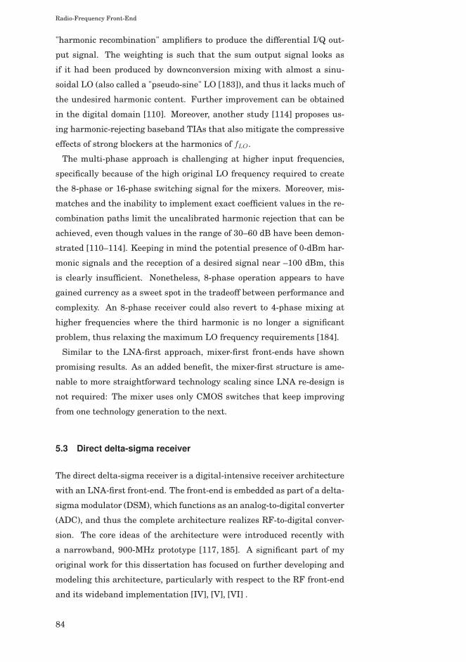
Radio-Frequency Front-End
"harmonic recombination" amplifiers to produce the differential I/Q out-
put signal. The weighting is such that the sum output signal looks as
if it had been produced by downconversion mixing with almost a sinu-
soidal LO (also called a "pseudo-sine" LO [183]), and thus it lacks much of
the undesired harmonic content. Further improvement can be obtained
in the digital domain [110]. Moreover, another study [114] proposes us-
ing harmonic-rejecting baseband TIAs that also mitigate the compressive
effects of strong blockers at the harmonics of fLO.
The multi-phase approach is challenging at higher input frequencies,
specifically because of the high original LO frequency required to create
the 8-phase or 16-phase switching signal for the mixers. Moreover, mis-
matches and the inability to implement exact coefficient values in the re-
combination paths limit the uncalibrated harmonic rejection that can be
achieved, even though values in the range of 30–60 dB have been demon-
strated [110–114]. Keeping in mind the potential presence of 0-dBm har-
monic signals and the reception of a desired signal near –100 dBm, this
is clearly insufficient. Nonetheless, 8-phase operation appears to have
gained currency as a sweet spot in the tradeoff between performance and
complexity. An 8-phase receiver could also revert to 4-phase mixing at
higher frequencies where the third harmonic is no longer a significant
problem, thus relaxing the maximum LO frequency requirements [184].
Similar to the LNA-first approach, mixer-first front-ends have shown
promising results. As an added benefit, the mixer-first structure is ame-
nable to more straightforward technology scaling since LNA re-design is
not required: The mixer uses only CMOS switches that keep improving
from one technology generation to the next.
5.3 Direct delta-sigma receiver
The direct delta-sigma receiver is a digital-intensive receiver architecture
with an LNA-first front-end. The front-end is embedded as part of a delta-
sigma modulator (DSM), which functions as an analog-to-digital converter
(ADC), and thus the complete architecture realizes RF-to-digital conver-
sion. The core ideas of the architecture were introduced recently with
a narrowband, 900-MHz prototype [117, 185]. A significant part of my
original work for this dissertation has focused on further developing and
modeling this architecture, particularly with respect to the RF front-end
and its wideband implementation [IV], [V], [VI] .
84

Radio-Frequency Front-End
Figure 5.4. (a) Conceptual diagram of a delta-sigma modulator and (b) a modulator witha linearized quantizer model.
Delta-sigma modulation itself is a data conversion technique based on
"oversampling" an input signal of bandwidth fBW [186]. In general, the
highest frequency content that can be sampled without aliasing is at the
Nyquist frequency, fN = fsample/2, where fsample is the sampling fre-
quency. For a DSM ADC, oversampling means that we have fBW � fN ,
and the oversampling ratio (OSR) is defined as fsample/2fBW . A subse-
quent attraction of a DSM is the reduction of quantization noise within
fBW , which in turn allows for a greater dynamic range and bit resolu-
tion [187].
The basic structure of a DSM ADC is shown in Figure 5.4(a). It consists
of a loop filter, H, a quantizer, Q, and digital-to-analog (D/A) converted
feedback from the output to the input. By linearizing the quantizer in
Figure 5.4(b), we obtain the transfer functions for the input signal (STF)
and the quantization noise (NTF) as follows:
STF =voutvin
=H
1 +H, (5.1)
NTF =voutvqn
=1
1 +H. (5.2)
There are a multitude of possible loop filters, but they can all be divided
into discrete-time (DT) and continuous-time (CT) structures, with H =
H(z) or H = H(s), respectively. If H is a lowpass function, equations 5.1
and 5.2 show that the desired signal will be lowpass filtered (STF) while
the quantization noise is highpass filtered (NTF). The latter fact gives rise
to the term "noise shaping," another attractive DSM feature. The number
and configuration of the loop filter stages depends on DSM performance
requirements, such as filtering, stability, and resolution [187]. DT modu-
lator stages are usually implemented with switched-capacitor structures,
whereas CT modulators use GmC or Opamp-RC integrators. However, it
85

Radio-Frequency Front-End
Figure 5.5. RF-centric conceptual diagram of a direct delta-sigma receiver.
should be kept in mind that even a CT modulator is ultimately a discrete-
time system due to the quantizer [188].
In communication applications, DSMs are used, for example, in base-
band A/D conversion, frequency synthesis, and audio signal D/A conver-
sion [189]. There have also been attempts to create RF sampling re-
ceivers based on DSM structures. These include bandpass sampling, pas-
sive direct-conversion sampling, and active direct-conversion sampling.
Many bandpass sampling receivers tend to suffer from limited tunabil-
ity and high power consumption due to a high gain bandwidth [190–192],
whereas mostly passive circuits provide a high degree of linearity but in-
ferior noise performance [173,174].
The recently introduced active direct delta-sigma receiver concept at-
tempts to navigate a tradeoff between these two approaches by providing
acceptable tunability, linearity, noise, and power consumption simultane-
ously. As shown in Figure 5.5, the DDSR combines the functionality of
an analog receiver front-end and a baseband DSM. This is done by apply-
ing delta-sigma feedback to the front-end blocks, thus embedding them
as part of the loop filter H(s). This assigns simultaneous dual roles to
these blocks: On the one hand, they function as conventional amplifi-
cation and downconversion stages, but on the other hand they function
as frequency-translating DSM integrator stages. In effect, the complete
structure becomes an RF-to-digital converter in which signal digitization
begins at RF.
Figure 5.6 depicts the block diagram of a generic DDSR, with added
detail in the RF-related sections. From a conventional RF point of view,
the first integrator is an LNA with an N-path filter connected in paral-
lel to its output node, vint. This provides amplification of the input RF
signal and filtering of blockers, depending on the size of CNpath and the
resistance of the passive mixer switches. At the same time, this arrange-
ment can be thought of as a GmC integrator, where "Gm" is the inter-
nal transconductance of the LNA and the frequency-translated "C" is a
86
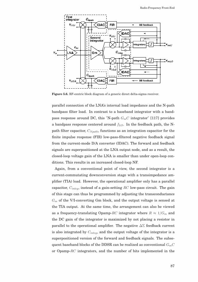
Radio-Frequency Front-End
Figure 5.6. RF-centric block diagram of a generic direct delta-sigma receiver.
parallel connection of the LNA’s internal load impedance and the N-path
bandpass filter load. In contrast to a baseband integrator with a band-
pass response around DC, this "N-path GmC integrator" [117] provides
a bandpass response centered around fLO. In the feedback path, the N-
path filter capacitor, CNpath, functions as an integration capacitor for the
finite impulse response (FIR) low-pass-filtered negative feedback signal
from the current-mode D/A converter (IDAC). The forward and feedback
signals are superpositioned at the LNA output node, and as a result, the
closed-loop voltage gain of the LNA is smaller than under open-loop con-
ditions. This results in an increased closed-loop NF.
Again, from a conventional point of view, the second integrator is a
current-commutating downconversion stage with a transimpedance am-
plifier (TIA) load. However, the operational amplifier only has a parallel
capacitor, Cinteg, instead of a gain-setting RC low-pass circuit. The gain
of this stage can thus be programmed by adjusting the transconductance
Gm of the V/I-converting Gm block, and the output voltage is sensed at
the TIA output. At the same time, the arrangement can also be viewed
as a frequency-translating Opamp-RC integrator where R ≈ 1/Gm and
the DC gain of the integrator is maximized by not placing a resistor in
parallel to the operational amplifier. The negative ΔΣ feedback current
is also integrated by Cinteg, and the output voltage of the integrator is a
superpositioned version of the forward and feedback signals. The subse-
quent baseband blocks of the DDSR can be realized as conventional GmC
or Opamp-RC integrators, and the number of bits implemented in the
87

Radio-Frequency Front-End
Figure 5.7. Comparison of an ideal and a real DDSR RF integrator response.
quantizer depends on the required performance.
DDSR RF design entails not only the conventional budgeting of analog
gain, noise, and linearity, but also the mapping of the two RF stages as
part of the CT loop filter, H(s), for proper modulator operation. This is a
new design approach that requires new guidelines. Accordingly, this leads
to the need for accurate analytical modeling, particularly because the first
RF integrator is highly non-ideal compared to a conventional baseband
GmC integrator. Some of the most important non-idealities can be seen in
Figure 5.7, which compares a sample RF integrator response to a corre-
sponding ideal GmC integrator whose frequency response has been trans-
lated from DC to around fLO = 2.5 GHz. First, the gain of the integrator at
fLO (that is, the "DC gain") is very limited due to the low internal RF out-
put impedance of the LNA. The figure also shows two other non-idealities
that follow from the N-path structure, as discussed in chapter 3, namely
the limited attenuation far away from fLO and the unsymmetrical band-
pass response around fLO. In addition, the integrator exhibits harmonic
folding, again as a consequence of the N-path structure.
As proposed in our original work in publication [IV], the LTI model of
the N-path filter can be used to incorporate the first three non-idealities
into the DDSR model for more reliable simulation results. The rest of
this section reviews some of the most important features of this proposed
approach. In the forward path shown in Figure 5.8(a), the LNA transcon-
88
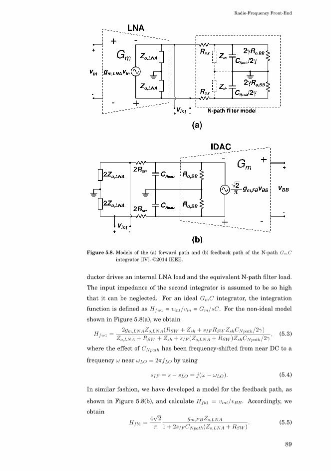
Radio-Frequency Front-End
Figure 5.8. Models of the (a) forward path and (b) feedback path of the N-path GmC
integrator [IV]. ©2014 IEEE.
ductor drives an internal LNA load and the equivalent N-path filter load.
The input impedance of the second integrator is assumed to be so high
that it can be neglected. For an ideal GmC integrator, the integration
function is defined as Hfw1 = vint/vin = Gm/sC. For the non-ideal model
shown in Figure 5.8(a), we obtain
Hfw1 =2gm,LNAZo,LNA(RSW + Zsh + sIFRSWZshCNpath/2γ)
Zo,LNA +RSW + Zsh + sIF (Zo,LNA +RSW )ZshCNpath/2γ, (5.3)
where the effect of CNpath has been frequency-shifted from near DC to a
frequency ω near ωLO = 2πfLO by using
sIF = s− sLO = j(ω − ωLO). (5.4)
In similar fashion, we have developed a model for the feedback path, as
shown in Figure 5.8(b), and calculate Hfb1 = vint/vBB. Accordingly, we
obtain
Hfb1 =4√2
π
gm,FBZo,LNA
1 + 2sIFCNpath(Zo,LNA +RSW ). (5.5)
89

Radio-Frequency Front-End
The transconductance of the baseband source is multiplied by the factor√2/π, because we are interested in the amount of charge upconverted to
the main harmonic of the LO. This factor is obtained from the correspond-
ing term in the Fourier series of an LO signal with a 25-% duty cycle.
It should be noted that this model of the feedback path loses accuracy for
complex LNA output impedances. However, it is simple and, in particular,
quite intuitive because the LNA output impedance is simply multiplied
by 2 since each baseband branch sees the impedance for only one half of
each LO period. This provides an accurate result for resistive LNA output
impedances. Improved accuracy for complex impedances can be obtained
by developing the results of the transmitter-focused upconversion-mixing
analysis in a prior study [193] for DDSR application.
To use these RF integrator models, the DDSR as a whole must be mod-
eled using a signal flow graph (SFG) that contains integration stages. The
sample s-domain SFG in Figure 5.9 contains only two stages so as to keep
the focus on the RF modeling. Similar to a baseband DSM, the SFG has
forward (ai) and feedback (bi) coefficients that relate the integrator stages
to the loop filter bandwidth, fBW = 1/2πT , where T is the integration
time constant. For simplicity, we assume that the quantizer gain aq = 1.
The SFG can then be used to calculate the STF and NTF as a function of
the loop filter coefficients.
Before doing so, we should recall that the DDSR is ultimately a discrete-
time system, even though the integrators operate in the continuous-time
domain. Full modeling thus requires z-domain analysis of the STF and
NTF. However, as discussed in publication [IV], the DDSR performs sig-
nal filtering in addition to noise shaping. This means that we will always
have fBW << fsample, and consequently the discretized in-band signal
(close to fLO at RF, close to DC at baseband) is a very close approxima-
tion of its continuous-time version. This DDSR feature enables us to use
continuous-time s-domain modeling to obtain a reliable approximation of
the receiver operation close to fLO.
To incorporate the effects of non-ideal integration into the CT model, the
modulator coefficients related to the first stage (a1 and b1) are replaced
by their non-ideal representations, as shown in Figure 5.9. The transfer
functions Hfw1 and Hfb1 both separately contain the integration function
1/sT . The STF and NTF approximations of the I branch for the two-stage
example are derived as follows:
90

Radio-Frequency Front-End
Figure 5.9. Signal flow graph of a sample two-stage DDSR with (upper) ideal and (lower)non-ideal representation of the N-path GmC integrator [IV]. ©2014 IEEE.
STFI =vout,Ivin
=1
2
a2Hrf
sIFT + b2 + a2Hfb, (5.6)
NTFI =vout,Ivqn
=sIFT
sIFT + b2 + a2Hfb. (5.7)
The analytical STF and NTF now contain the two non-ideal integra-
tion functions, and the N-path GmC integrator can be designed according
to the required DDSR behavior. For example, by inserting Hfb into the
equation for NTFI , the original work presented in publication [V] showed
that one of the two NTF zeros in this two-stage example (that is, two
integrators) is dependent on the LNA output impedance and CNpath. It
should be as close as possible to the origin for best in-band noise shaping
performance, as discussed further in publication [V]. In particular, the
analysis demonstrated that LNA output impedance should be maximized
to move the zero towards the origin. Moreover, the analysis showed that
the sizing of capacitor CNpath governs a system-wide tradeoff between the
DDSR noise figure, noise shaping, and blocker filtering. Publication [V]
details this tradeoff and proposes a practical method for obtaining a suit-
able compromise in light of performance specifications.
91

Radio-Frequency Front-End
Figure 5.10. Signal flow graph of the four-stage wideband DDSR. The underlined ΔΣ
modulator coefficients are programmable [VI]. ©2014 IEEE.
The second RF integrator can be modeled in the same manner as the
first stage. This provides an even more accurate understanding of how
RF stage properties affect DDSR behavior as a whole. However, the non-
idealities of the second stage are much less severe than those of the first
stage, and modeling is thus not an absolute requirement.
5.4 Experimental work
Two DDSR RF front-ends in 40-nm CMOS were designed as original con-
tributions of this dissertation. First, I designed a narrowband version for
2.5 GHz, which was discussed in chapter 3, and for which I did further
analysis in publications [VII] and [125]. Second, I designed a wideband
version for 0.7–2.7 GHz [VI], which is discussed further in this section
within the context of DDSR operation.
The signal flow graph of the experimental DDSR is shown in Figure
5.10. It has four stages, and the loop filter baseband bandwidth could be
programmed as approximately 1.5 or 15 MHz. This allowed for input RF
signals with bandwidths of up to 20 MHz. Beyond this value, the signal
to noise and distortion ratio (SNDR) began to degrade due to increasing
quantization noise at the channel edge. The receiver used 1.5-bit quanti-
zation to reduce the total amount of quantization noise. Furthermore, the
internal feedback, g2, implemented an NTF notch to improve the SNDR
close to the channel edge, and a finite impulse response (FIR) lowpass
filter in the outermost feedback loop reduced the amount of quantization
noise that was transferred to the LNA output node.
As explained in the previous section, the RF front-end comprised the
92

Radio-Frequency Front-End
Figure 5.11. Schematic of the experimental wideband DDSR front-end [VI]. ©2014IEEE.
two first stages in the signal flow graph. Figure 5.11 shows the structure
of the front-end, following the generic structure presented previously in
Figure 5.6. From a conventional point of view, the LNA was loaded by
a blocker-filtering N-path structure that relaxed the out-of-band linearity
requirements of the subsequent stages. The RF signal was then processed
further by a second amplifier stage, which worked as a transconductor
in a current-mode downconversion interface that drove a TIA. To enable
a stand-alone analog front-end measurement through internal test I/O
pins, a resistor could be connected in parallel to the TIA to set the gain
and bandwidth of the second stage; the rest of the baseband blocks were
powered down. The implemented circuit was differential, but it is drawn
here as single-ended for the sake of simplicity.
As discussed earlier, from the DDSR point of view these two stages func-
tioned as frequency-translating integrators. The output of the first inte-
grator was sensed at RF and that of the second integrator at baseband.
D/A-converted, current-mode feedback was integrated by both stages and
superpositioned with the forward signal.
In the first integrator, the LNA was a common-source amplifier with
a wideband PMOS load and a tunable active-RC shunt-shunt feedback
for intrinsically wideband input matching. The input matching (S11) of a
shunt-shunt LNA is dependent on its load, and thus the bandpass N-path
filter resulted in a bandpass matching response around fLO at the input.
Because of the parasitic capacitance at the LNA output node, the N-path
filter response was increasingly detuned from fLO at higher operating fre-
quencies. The cross-coupled baseband transconductors, Gmx [104], pro-
vided a polyphase response that could be used to shift the bandpass peak
back to fLO, with a minor noise penalty due in particular to the upcon-
verted 1/f noise.
93

Radio-Frequency Front-End
The second integrator was a transconductance amplifier that drove the
passive downconversion mixer and consisted of a current-reusing common-
drain–common-source amplifier. This boosted the equivalent transcon-
ductance as compared to a simple common-drain amplifier, while still
maintaining low output impedance for wideband operation. The low out-
put impedance as such was a tradeoff between bandwidth (due to the RC
pole frequency being relatively high) and its operation as a transconductor
because, from the latter perspective, it should ideally be infinite. Three in-
dividually switchable cells were connected in parallel to enable gain tun-
ing, and the inversion at the input of the common-source device was done
by using the signal from the opposite differential branch.
To improve the linearity of the downconversion interface, the capaci-
tor Cvg practically extended the virtual-ground performance of the opera-
tional amplifier beyond the point where the amplifier gain began to drop.
This ensured the lack of large voltage swings in the interface. Cvg was ef-
fectively in parallel to the integration capacitor, Cint, but it did not disturb
the operation of the integrator. This was due to the Miller effect and the
high DC gain of the operational amplifier (40–50 dB), causing Cint to be
seen at the amplifier input as a substantially larger capacitor than Cvg.
The measured differential-mode S11 of the 0.7–2.7-GHz DDSR is shown
in Figure 5.12 for fLO = 2 GHz. As mentioned previously, the S11 of the
LNA was affected by its load circuit and was thus a bandpass function.
Moreover, the effect of the ΔΣ feedback was visible within the sample 1.5-
MHz bandwidth of the loop filter through the inverted notch. The cross-
coupled baseband transconductors Gmx were used to center the matching
response at 2 GHz.
Figure 5.13 shows a sample baseband output spectrum of the DDSR at
fLO = 2.5 GHz. Three items in particular deserve to be mentioned. First,
a –68-dBm input signal at 2.5001 GHz was amplified and downconverted
by the receiver. Second, the quantization noise was shaped away from
the desired channel (in this case, the RF bandwidth was 15 MHz and the
baseband bandwidth was thus 7.5 MHz), as is expected of a DSM in gen-
eral. Third, a –43-dBm interferer signal at 2.5875 GHz was filtered by
the receiver loop, and effectively disappeared into the noise floor. The be-
havior was very similar at other LO frequencies throughout the operating
range.
The IIP3 of the receiver is plotted in Figure 5.14 against the frequency of
the closest interferer. The two interferer tones were spaced such that the
94

Radio-Frequency Front-End
Figure 5.12. Measured wideband DDSR RF input matching when fLO = 2.0 GHz.
Figure 5.13. Measured wideband DDSR output spectrum.
95
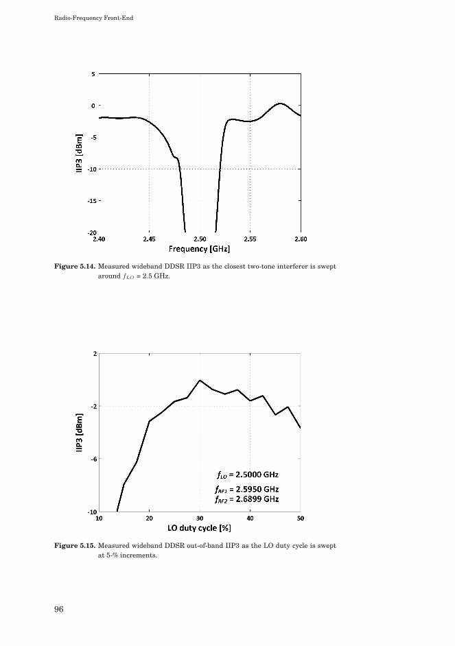
Radio-Frequency Front-End
Figure 5.14. Measured wideband DDSR IIP3 as the closest two-tone interferer is sweptaround fLO = 2.5 GHz.
Figure 5.15. Measured wideband DDSR out-of-band IIP3 as the LO duty cycle is sweptat 5-% increments.
96
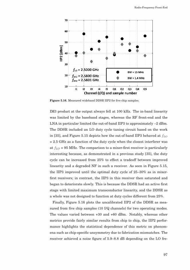
Radio-Frequency Front-End
Figure 5.16. Measured wideband DDSR IIP2 for five chip samples.
IM3 product at the output always fell at 100 kHz. The in-band linearity
was limited by the baseband stages, whereas the RF front-end and the
LNA in particular limited the out-of-band IIP3 to approximately –2 dBm.
The DDSR included an LO duty cycle tuning circuit based on the work
in [35], and Figure 5.15 depicts how the out-of-band IIP3 behaved at fLO= 2.5 GHz as a function of the duty cycle when the closest interferer was
at fLO + 95 MHz. The comparison to a mixer-first receiver is particularly
interesting because, as demonstrated in a previous study [35], the duty
cycle can be increased from 25% to effect a tradeoff between improved
linearity and a degraded NF in such a receiver. As seen in Figure 5.15,
the IIP3 improved until the optimal duty cycle of 25–30% as in mixer-
first receivers; in contrast, the IIP3 in this receiver then saturated and
began to deteriorate slowly. This is because the DDSR had an active first
stage with limited maximum transconductor linearity, and the DDSR as
a whole was not designed to function at duty cycles different from 25%.
Finally, Figure 5.16 plots the uncalibrated IIP2 of the DDSR as mea-
sured from five chip samples (10 I/Q channels) for two operating modes.
The values varied between +30 and +60 dBm. Notably, whereas other
metrics provide fairly similar results from chip to chip, the IIP2 perfor-
mance highlights the statistical dependence of this metric on phenom-
ena such as chip-specific unsymmetry due to fabrication mismatches. The
receiver achieved a noise figure of 5.9–8.8 dB depending on the LO fre-
97

Radio-Frequency Front-End
Parameter Value
fLO [GHz] 0.7–2.7
fclk [GHz] 1.25
RF signal bandwidth [MHz] 15
NF [dB] 5.9–8.8
OB-IIP3 [dBm] –2
IIP2 [dBm] > +38
B–1dBCP [dBm] –12
Maximum SNDR [dB] 43
VDD [V] 1.1
Power [mW] 90
Active area [mm2] 1.0
CMOS technology [nm] 40
Table 5.1. Performance summary of the direct delta-sigma receiver (for the linearity mea-surements, the closest interferer is at fLO + 80 MHz (IIP2), fLO + 92.5 MHz(B–1dBCP), or fLO + 95 MHz (OB-IIP3)).
quency, and it was able to tolerate blockers of up to –12 dBm at a distance
of 92.5 MHz from the LO before the in-band gain was compressed by 1 dB.
The RF front-end, including the LO buffering circuitry, consumed 45 mA
from 1.1 V at fLO = 1.7 GHz. The performance of the wideband DDSR is
summarized in Table 5.1 and additional measured metrics are provided
in publication [VI].
In summary, the direct delta-sigma receiver is a digital-intensive archi-
tecture that pushes the A/D conversion interface from baseband up to RF,
that is to say, towards the antenna. The RF front-end blocks operate in
dual roles simultaneously, a fact that has resulted in the development of
the presented new approach for front-end modeling and design. In view of
the performance metrics required of a SAW-less SDR, the achieved exper-
imental results for the wideband DDSR show that further work is needed,
especially with respect to the receiver’s ability to tolerate strong blocker
signals without gain compression. Moreover, the first integrator suffers
from signal folding from the harmonics of fLO, pointing to the need for
further developing aspects of the N-path filtering.
98

6. Conclusions
This dissertation and the related scientific publications [I]-[VII] have cov-
ered a number of key challenges that the complete integration of a wire-
less receiver currently faces. The challenges include the use of off-chip fil-
ters and resonators with poor tunability, the consequent need for parallel
receive paths in multi-standard receivers, and the use of external compo-
nents when generating suitable power supply voltages. The dissertation
has also presented and analyzed approaches towards overcoming those
challenges, specifically high-Q component integration for interferer fil-
tering and low-noise oscillator design, DC-DC converter integration, and
digital-intensive receiver operation. From a general point of view, all of
these techniques target the creation of a fully integrated cellular receiver
that lives up to the SDR paradigm.
First, high-Q N-path filtering was implemented within a 2.5-GHz ex-
perimental receiver front-end in 40-nm CMOS, as detailed in chapter 3
and publication [VII]. The filtering was implemented in parallel to the in-
ternal LC load of an LNA, thus providing a further sharpened frequency
response at that particular RF node. Depending on the level of Q-boosting,
this provided up to more than 15 dB of programmable RF interferer fil-
tering at an offset of 50 MHz from the center frequency, thus relaxing the
small-signal linearity requirements of the post-LNA stages. This particu-
lar Q-boosting technique also increased the absolute gain at the interferer
frequency, which required gain reduction in the case of very strong block-
ers as a sensitivity drawback. The counter-intuitive dependence of the
LNA gain on the mixer switch resistance in the N-path filter is analyzed
in detail in publication [VII], but the limitations imposed by input device
non-linearity require further study.
Second, a high-Q above-IC FBAR was used as a resonator in a 2.1-GHz
VCO that was implemented in 0.25-μm BiCMOS. The results demon-
99
Conclusions
strated the feasibility of such IC/FBAR co-integration and exhibited a
VCO phase noise improvement of up to 20 dBc/Hz compared to a refer-
ence LC VCO design. However, using the mechanical FBAR also resulted
in an expected frequency tuning range reduction to only 37 MHz, although
the choice of VCO architecture provided a greater tuning range than any
other published at the time [I]. The frequency accuracy of the above-
IC resonator is another concern that has been studied at great length
since the VCO was designed, with approaches such as changed fabrica-
tion techniques and temperature compensation providing improved yield.
Furthermore, the question of start-up robustness in the face of above-IC
fabrication defects was analyzed, with the results in chapter 3 and publi-
cation [II] demonstrating that this particular VCO design can start even
if the Q dropped by one order of magnitude.
Third, the feasibility of DC-DC converter integration was examined by
implementing a buck converter in 65-nm CMOS. The design presented in
chapter 4 and publication [III] featured a synchronously switched cascode
structure for operation with a regular 3.6-V battery, and it provided a 1.8-
V supply and more than 150 mA of drive capability for the load circuit.
The power-loss components in the cascode were analyzed to show that
non-uniform device sizing is one possible way of enhancing the power ef-
ficiency, η. Furthermore, the proper manner of stacking CMOS devices
vertically was investigated in order to produce design guidelines, with
the minimization of inductive coupling and eddy currents being the main
points of focus. The achieved nominal η = 67.9% is considerably higher
than what can be achieved with an integrated linear regulator, but the
output voltage ripple of 294 mV is too high to directly use the converter
for powering most other practical systems. The ripple can be decreased
by, for example, further increasing the switching frequency and the out-
put filter capacitor size, although both of these approaches lead to other
tradeoffs.
Finally, the recently introduced direct delta-sigma receiver was used as
a case study in the development of digital-intensive receiver structures
that move A/D conversion towards the antenna interface. For the pur-
poses of this dissertation, particular emphasis was put on the role and
modeling of the RF stages, both in chapter 5 and in publication [IV]. It was
demonstrated that the stages function simultaneously as conventional
amplifiers and/or downconverters on the one hand, and as non-ideal in-
tegrators in a frequency-translating ΔΣ A/D converter on the other. This
100

Conclusions
leads to tradeoffs, and suitable design guidelines for the LNA-centric first
stage were proposed in publication [V]. A 0.7–2.7-GHz wideband receiver
was designed as a prototype in 40-nm CMOS, including a programmable
RF front-end implemented by the author. As detailed in publication [VI],
a noise figure of 5.9–8.8 dB was obtained along with an out-of-band IIP3
of –2 dBm. Improved tolerance against strong interferer signals and the
rejection of harmonic content were identified as two of the main areas of
RF front-end development in this type of receiver.
The method for replacing current off-chip wireless receiver functions
and/or components with their integrated versions can in principle be di-
vided into special component technology and circuit-level solutions. The
FBAR in the VCO and the high-Q inductor in the buck converter are ex-
amples of the former, and they provide the required functionality with
some tradeoffs. However, one of the major drawbacks is the cost asso-
ciated with the required extra manufacturing steps, which is added to
the regular costs of fabricating CMOS/BiCMOS circuits. The use of these
components thus becomes a case-by-case exercise in evaluating the pros
against the cons. In other words, are the benefits and performance of a
fully integrated solution sufficient compared to current standard indus-
trial solutions when accounting for the costs?
In any case, it appears possible that high-efficiency switched-mode DC-
DC converters will be fully integrated with the receiver that they supply.
Regardless of the chosen switched-mode technology, strict attention must
be paid to the output ripple spectrum of the converter. Similar to trans-
mitter leakage in FDD transceivers, the emitted spectrum must be such
that is does not compromise RF signal reception at the required sensitiv-
ity level, neither through electromagnetic radiation nor through leakage
due to limited high-frequency power-supply rejection in the RF front-end
circuits. When comparing architectures, the switched-capacitor converter
is better situated in the integration race, particularly because of its com-
patibility with technology scaling and because it does not need special
fabrication steps.
The use of circuit-level solutions as opposed to specialized component
fabrication is also attractive for SDR realization, particularly as it relates
to reducing parallelism and using digital-intensive signal processing tech-
niques. In this regard, the wideband front-end approach is a popular re-
search avenue for realizing programmability and reducing the number of
non-concurrent receiver chains in an SDR. Moreover, frequency-tunable
101

Conclusions
N-path filtering is in this context a potential replacement for non-tunable
pre-select filters in both LNA-first and mixer-first receivers, including the
direct delta-sigma receiver. The questions of limited selectivity and rejec-
tion of harmonics still need to be solved to full satisfaction, but current
progress is promising in view of future industrial adoption.
102

Bibliography
[1] T. K. Sarkar, R. J. Mailloux, A. A. Oliner, M. Salazar-Palma, and D. L.Sengupta, History of Wireless. Hoboken: Wiley-IEEE, 2006.
[2] L. Coe, Wireless Radio: A History. McFarland & Company, Inc., 2006.
[3] Radio Regulations. Geneva: International Telecommunication Union,2012, vol. 1.
[4] B. P. Lathi and Z. Ding, Modern Digital and Analog Communication Sys-tems, 4th ed. New York: Oxford University Press, 2009.
[5] S. Haykin and M. Moher, Introduction to Analog & Digital Communica-tions, 2nd ed. Hoboken: John Wiley & Sons, 2007.
[6] D. Kaczman, M. Shah, M. Alam, M. Rachedine, D. Cashen, L. Han, andA. Raghavan, “A single-chip 10-band WCDMA/HSDPA 4-band GSM/EDGESAW-less CMOS receiver with DigRF 3G interface and +90 dbm IIP2,”IEEE Journal of Solid-State Circuits, vol. 44, no. 3, pp. 718–739, Mar.2009.
[7] A. Abidi, “Low-power radio-frequency ICs for portable communications,”Proceedings of the IEEE, vol. 83, no. 4, pp. 544–569, Apr. 1995.
[8] P. Baltus and R. Dekker, “Optimizing RF front ends for low power,” Pro-ceedings of the IEEE, vol. 88, no. 10, pp. 1546–1559, Oct. 2000.
[9] A. Pärssinen, “Multimode-multiband transceivers for next generation ofwireless communications,” in Proc. Eur. Solid-State Circ. Conf., 2011, pp.25–36.
[10] L. Larson, “RF and microwave hardware challenges for future radio spec-trum access,” Proceedings of the IEEE, vol. 102, no. 3, pp. 321–333, Mar.2014.
[11] M.-A. Dubois, C. Billard, G. Parat, M. Aissi, H. Ziad, J.-F. Carpentier,and K. B. Östman, “Above-IC integration of BAW resonators and filtersfor communication applications,” in Proceedings of the 3rd InternationalSymposium on Acoustic Wave Devices for Future Mobile Communications,2007, pp. 111–115.
[12] M.-A. Dubois, “Monolithic integration,” in RF Bulk Acoustic Wave Filtersfor Communications, K.-y. Hashimoto, Ed. Boston and London: ArtechHouse, 2009.
103

Bibliography
[13] E. Armstrong, “Wireless receiving system,” U.S. Patent 1,113,149, 1914.
[14] ——, “Some recent developments of regenerative circuits,” Proceedings ofthe Institute of Radio Engineers, vol. 10, no. 4, pp. 244–260, 1922.
[15] ——, “The super-heterodyne-its origin, development, and some recent im-provements,” Proceedings of the Institute of Radio Engineers, vol. 12, no. 5,pp. 539–552, 1924.
[16] P.-I. Mak, S.-P. U, and R. Martins, “Transceiver architecture selection: Re-view, state-of-the-art survey and case study,” IEEE Circuits and SystemsMagazine, vol. 7, no. 2, pp. 6–25, 2007.
[17] HF/50 MHz Transceiver FTdx5000 Series Operating Manual, YaesuMusen Co., Ltd., 2013.
[18] A. Abidi, “Direct-conversion radio transceivers for digital communica-tions,” IEEE Journal of Solid-State Circuits, vol. 30, no. 12, pp. 1399–1410,Dec. 1995.
[19] N. Pletcher, S. Gambini, and J. Rabaey, “A 52 μW wake-up receiver with–72 dBm sensitivity using an uncertain-IF architecture,” IEEE Journal ofSolid-State Circuits, vol. 44, no. 1, pp. 269–280, Jan. 2009.
[20] B. Razavi, “Design of millimeter-wave CMOS radios: A tutorial,” IEEETransactions on Circuits and Systems I: Regular Papers, vol. 56, no. 1, pp.4–16, Jan. 2009.
[21] ——, “Design considerations for direct-conversion receivers,” IEEE Trans-actions on Circuits and Systems II: Analog and Digital Signal Processing,vol. 44, no. 6, pp. 428–435, Jun. 1997.
[22] R. Meyer and A. Wong, “Blocking and desensitization in RF amplifiers,”IEEE Journal of Solid-State Circuits, vol. 30, no. 8, pp. 944–946, Aug.1995.
[23] A. Mirzaei, H. Darabi, and D. Murphy, “A low-power process-scalablesuper-heterodyne receiver with integrated high-Q filters,” IEEE Journalof Solid-State Circuits, vol. 46, no. 12, pp. 2920–2932, Dec. 2011.
[24] J. Mitola, “The software radio architecture,” IEEE Communications Mag-azine, vol. 33, no. 5, pp. 26–38, 1995.
[25] J. Mitola and G. Maguire Jr., “Cognitive radio: making software radiosmore personal,” IEEE Personal Communications, vol. 6, no. 4, pp. 13–18,1999.
[26] ANAN-10 Transceiver Technical Specifications, Apache Labs, 2014.
[27] P. Kenington and L. Astier, “Power consumption of a/d converters forsoftware radio applications,” IEEE Transactions on Vehicular Technology,vol. 49, no. 2, pp. 643–650, Feb. 2000.
[28] R. Staszewski, “Digital RF and digitally-assisted RF,” in IEEE Interna-tional Symposium on Radio-Frequency Integration Technology, Nov. 2011,pp. 9–16.
104

Bibliography
[29] C. Campbell, “Applications of surface acoustic and shallow bulk acousticwave devices,” Proceedings of the IEEE, vol. 77, no. 10, pp. 1453–1484,Oct. 1989.
[30] K. Lakin, “Thin film resonator technology,” IEEE Transactions on Ultra-sonics, Ferroelectrics and Frequency Control, vol. 52, no. 5, pp. 707–716,May 2005.
[31] K.-y. Hashimoto, Ed., RF Bulk Acoustic Wave Filters for Communications.Boston and London: Artech House, 2009.
[32] A. Mirzaei and H. Darabi, “A low-power WCDMA transmitter with an in-tegrated notch filter,” IEEE Journal of Solid-State Circuits, vol. 43, no. 12,pp. 2868–2881, Dec. 2008.
[33] M. Mikhemar, H. Darabi, and A. Abidi, “A tunable integrated duplexerwith 50dB isolation in 40nm CMOS,” in IEEE International Solid-StateCircuits Conference Digest of Technical Papers, Feb. 2009, pp. 386–387,387a.
[34] ——, “A multiband RF antenna duplexer on CMOS: Design and perfor-mance,” IEEE Journal of Solid-State Circuits, vol. 48, no. 9, pp. 2067–2077,Sept. 2013.
[35] M. Kaltiokallio, R. Valkonen, K. Stadius, and J. Ryynanen, “A 0.7-2.7-GHzblocker-tolerant compact-size single-antenna receiver for wideband mobileapplications,” IEEE Transactions on Microwave Theory and Techniques,vol. 61, no. 9, pp. 3339–3349, Sept. 2013.
[36] D. Bockelman and W. Eisenstadt, “Combined differential and common-mode scattering parameters: theory and simulation,” IEEE Transactionson Microwave Theory and Techniques, vol. 43, no. 7, pp. 1530–1539, Jul.1995.
[37] W. Eisenstadt, B. Stengel, and B. Thompson, Microwave Differential Cir-cuit Design Using Mixed-Mode S-Parameters. Boston and London: ArtechHouse, 2006.
[38] A. Pärssinen, “Direct conversion receivers in wide-band systems,” Ph.D.dissertation, Helsinki University of Technology, 2000.
[39] J. Kaukovuori, “CMOS radio frequency circuits for short-range direct-conversion receivers,” Ph.D. dissertation, Helsinki University of Technol-ogy, 2008.
[40] H. Friis, “Noise figures of radio receivers,” Proceedings of the IRE, vol. 32,no. 7, pp. 419–422, 1944.
[41] C. Iversen and T. E. Kolding, “Noise and intercept point calculation formodern radio receiver planning,” IEE Proceedings-Communications, vol.148, no. 4, pp. 255–259, 2001.
[42] D. Manstretta, M. Brandolini, and F. Svelto, “Second-order intermodula-tion mechanisms in CMOS downconverters,” IEEE Journal of Solid-StateCircuits, vol. 38, no. 3, pp. 394–406, Mar. 2003.
105
Bibliography
[43] V. Aparin and L. Larson, “Analysis and reduction of cross-modulation dis-tortion in CDMA receivers,” IEEE Transactions on Microwave Theory andTechniques, vol. 51, no. 5, pp. 1591–1602, May 2003.
[44] J. Ryynanen, S. Lindfors, K. Stadius, and K. A. I. Halonen, “Integratedcircuits for multiband multimode receivers,” IEEE Circuits and SystemsMagazine, vol. 6, no. 2, pp. 5–16, 2006.
[45] 3rd Generation Partnership Project; Technical Specification GroupGSM/EDGE Radio Access Network; Radio transmission and reception (Re-lease 12), Std., Rev. 3GPP TS 45.005 v12.1.0, November 2013.
[46] 3rd Generation Partnership Project; Technical Specification Group RadioAccess Network; User Equipment (UE) radio transmission and reception(FDD) (Release 12), Std., Rev. 3GPP TS 25.101 v12.2.0, December 2013.
[47] 3rd Generation Partnership Project; Technical Specification Group RadioAccess Network; Evolved Universal Terrestrial Radio Access (E-UTRA);User Equipment (UE) radio transmission and reception (Release 12), Std.,Rev. 3GPP TS 36.101 v12.2.0, December 2013.
[48] A. Springer, L. Maurer, and R. Weigel, “RF system concepts for highly inte-grated RFICs for W-CDMA mobile radio terminals,” IEEE Transactions onMicrowave Theory and Techniques, vol. 50, no. 1, pp. 254–267, Jan. 2002.
[49] J. Ryynänen, “Low-noise amplifiers for integrated multi-mode direct-conversion receivers,” Ph.D. dissertation, Helsinki University of Technol-ogy, 2004.
[50] H. Darabi, “CMOS transceivers for modern cellular terminals,” in Ad-vances in Analog and RF IC Design for Wireless Communication Systems,G. Manganaro and D. Leenaerts, Eds. Oxford: Academic Press, 2013.
[51] C. Svensson, “The blocker challenge when implementing software definedradio receiver RF frontends,” Analog Integrated Circuits and Signal Pro-cessing, vol. 64, no. 2, pp. 81–89, 2010.
[52] E. Atalla, A. Bellaouar, and P. Balsara, “IIP2 requirements in 4G LTEhandset receivers,” in IEEE International Midwest Symposium on Circuitsand Systems, Aug. 2013, pp. 1132–1135.
[53] E. Mollick, “Establishing Moore’s law,” IEEE Annals of the History of Com-puting, vol. 28, no. 3, pp. 62–75, Jul.-Sept. 2006.
[54] L. Larson, “Integrated circuit technology options for RFICs - present statusand future directions,” IEEE Journal of Solid-State Circuits, vol. 33, no. 3,pp. 387–399, Mar. 1998.
[55] T. Lee and S. Wong, “CMOS RF integrated circuits at 5 GHz and beyond,”Proceedings of the IEEE, vol. 88, no. 10, pp. 1560–1571, Oct. 2000.
[56] A. Abidi, “RF CMOS comes of age,” IEEE Journal of Solid-State Circuits,vol. 39, no. 4, pp. 549–561, Apr. 2004.
[57] M. Steyaert, M. Borremans, J. Craninckx, J. Crols, J. Janssens, andP. Kinget, “RF integrated circuits in standard CMOS technologies,” in Proc.Eur. Solid-State Circ. Conf., 1996, pp. 11–18.
106
Bibliography
[58] H.-S. P. Wong, D. Frank, P. Solomon, C. Wann, and J. Welser, “NanoscaleCMOS,” Proceedings of the IEEE, vol. 87, no. 4, pp. 537–570, Apr. 1999.
[59] B. Razavi, “CMOS technology characterization for analog and RF design,”IEEE Journal of Solid-State Circuits, vol. 34, no. 3, pp. 268–276, Mar.1999.
[60] H. Bennett, R. Brederlow, J. Costa, P. Cottrell, W. Huang, A. Immorlica,J.-E. Mueller, M. Racanelli, H. Shichijo, C. Weitzel, and B. Zhao, “Deviceand technology evolution for Si-based RF integrated circuits,” IEEE Trans-actions on Electron Devices, vol. 52, no. 7, pp. 1235–1258, Jul. 2005.
[61] K. Muhammad, R. Staszewski, and D. Leipold, “Digital RF processing:toward low-cost reconfigurable radios,” IEEE Communications Magazine,vol. 43, no. 8, pp. 105–113, 2005.
[62] L. Lewyn, T. Ytterdal, C. Wulff, and K. Martin, “Analog circuit design innanoscale CMOS technologies,” Proceedings of the IEEE, vol. 97, no. 10,pp. 1687–1714, Oct. 2009.
[63] Overall Roadmap Technology Characteristics Table, International Technol-ogy Roadmap for Semiconductors, Std., 2013.
[64] K. Wang, A. Swaminathan, and I. Galton, “Spurious tone suppressiontechniques applied to a wide-bandwidth 2.4 GHz fractional-N PLL,” IEEEJournal of Solid-State Circuits, vol. 43, no. 12, pp. 2787–2797, Dec. 2008.
[65] J. Stauth and S. Sanders, “Power supply rejection for RF amplifiers: The-ory and measurements,” IEEE Transactions on Microwave Theory andTechniques, vol. 55, no. 10, pp. 2043–2052, Oct. 2007.
[66] P. H. Woerlee, M. Knitel, R. van Langevelde, D. Klaassen, L. Tiemei-jer, A. Scholten, and A. Zegers-van Duijnhoven, “RF-CMOS performancetrends,” IEEE Transactions on Electron Devices, vol. 48, no. 8, pp. 1776–1782, Aug. 2001.
[67] S. Kang, B. Choi, and B. Kim, “Linearity analysis of CMOS for RF appli-cation,” IEEE Transactions on Microwave Theory and Techniques, vol. 51,no. 3, pp. 972–977, Mar. 2003.
[68] T. Lee, The Design of CMOS Radio-Frequency Integrated Circuits, 2nd ed.Cambridge: Cambridge University Press, 2003.
[69] Y. Chang, J. Leete, Z. Zhou, M. Vadipour, Y.-T. Chang, and H. Darabi, “Adifferential digitally controlled crystal oscillator with a 14-bit tuning res-olution and sine wave outputs for cellular applications,” IEEE Journal ofSolid-State Circuits, vol. 47, no. 2, pp. 421–434, Feb. 2012.
[70] M. Dubois, J.-F. Carpentier, P. Vincent, C. Billard, G. Parat, C. Muller,P. Ancey, and P. Conti, “Monolithic above-IC resonator technology for inte-grated architectures in mobile and wireless communication,” IEEE Jour-nal of Solid-State Circuits, vol. 41, no. 1, pp. 7–16, Jan. 2006.
[71] S. Dossou, N. Abele, E. Cesar, P. Ancey, J.-F. Carpentier, P. Vincent, and J.-M. Fournier, “60 μW SMR BAW oscillator designed in 65nm CMOS tech-nology,” in IEEE International Symposium on Circuits and Systems, 2008,pp. 1456–1459.
107

Bibliography
[72] R. Ruby, “Review and comparison of bulk acoustic wave FBAR, SMR tech-nology,” in IEEE Ultrasonics Symposium, 2007, pp. 1029–1040.
[73] M. Mark and J. Rabaey, “A 13.2 mW 1.9 GHz interpolative BAW-basedVCO for miniaturized RF frequency synthesis,” in IEEE InternationalSymposium on Circuits and Systems, 2009, pp. 1441–1444.
[74] M. Norling, J. Enlund, I. Katardjiev, and S. Gevorgian, “Oscillators basedon monolithically integrated AlN TFBARs,” IEEE Transactions on Mi-crowave Theory and Techniques, vol. 56, no. 12, pp. 3209–3216, Dec. 2008.
[75] D. Petit, E. Cesar, P. Bar, S. Joblot, G. Parat, O. Berchaud, J. Verdier, andJ. F. Carpentier, “Temperature compensated BAW resonator and its inte-grated thermistor for a 2.5GHz electrical thermally compensated oscilla-tor,” in IEEE Radio Frequency Integrated Circuits Symposium, Jun. 2009,pp. 339–342.
[76] R. Aigner, “High performance RF-filters suitable for above IC integra-tion: film bulk-acoustic-resonators (FBAR) on silicon,” in Proceedings ofthe IEEE Custom Integrated Circuits Conference, 2003, pp. 141–146.
[77] R. Ruby, M. Small, F. Bi, D. Lee, L. Callaghan, R. Parker, and S. Ortiz,“Positioning FBAR technology in the frequency and timing domain,” IEEETransactions on Ultrasonics, Ferroelectrics and Frequency Control, vol. 59,no. 3, pp. 334–345, Mar. 2012.
[78] K.-Y. Hashimoto, S. Tanaka, and M. Esashi, “Tunable RF SAW/BAW fil-ters: Dream or reality?” in Joint Conference of the IEEE InternationalFrequency Control and the European Frequency and Time Forum, 2011,pp. 1–8.
[79] S. Gevorgian and A. Vorobiev, “Tunable FBARs: Intrinsic vs. extrinsic tun-ability,” in IEEE MTT-S International Microwave Symposium Digest, Jun.2012, pp. 1–3.
[80] J. Larson III, R. Bradley, S. Wartenberg, and R. Ruby, “ModifiedButterworth-Van Dyke circuit for FBAR resonators and automated mea-surement system,” in IEEE Ultrasonics Symposium, vol. 1, 2000, pp. 863–868.
[81] H. Jin, S. Dong, J. Luo, and W. Milne, “Generalised Butterworth-Van Dykeequivalent circuit for thin-film bulk acoustic resonator,” Electronics Let-ters, vol. 47, no. 7, pp. 424–426, 2011.
[82] E. Kerherve, P. Ancey, M. Aid, and A. Kaiser, “BAW technologies: Devel-opment and applications within MARTINA, MIMOSA and MOBILIS ISTEuropean projects,” in IEEE Ultrasonics Symposium, 2006, pp. 341–350.
[83] C. Enz, J. Chabloz, J. Baborowski, C. Muller, and D. Ruffieux, “Buildingblocks for an ultra low-power MEMS-based radio,” in IEEE InternationalWorkshop on Radio-Frequency Integration Technology, 2007, pp. 158–167.
[84] R. Ruby, P. Bradley, I. Larson, J., Y. Oshmyansky, and D. Figueredo, “Ultra-miniature high-Q filters and duplexers using FBAR technology,” in IEEEInternational Solid-State Circuits Conference Digest of Technical Papers,2001, pp. 120–121.
108
Bibliography
[85] R. Ruby, P. Bradley, D. Clark, D. Feld, T. Jamneala, and K. Wang, “Acous-tic FBAR for filters, duplexers and front end modules,” in IEEE MTT-SInternational Microwave Symposium Digest, vol. 2, 2004, pp. 931–934.
[86] W. Pang, R. Ruby, R. Parker, P. Fisher, M. Unkrich, and J. Larson, “Atemperature-stable film bulk acoustic wave oscillator,” IEEE Electron De-vice Letters, vol. 29, no. 4, pp. 315–318, Apr. 2008.
[87] J. Hu, R. Parker, R. Ruby, and B. Otis, “A wide-tuning digitally controlledFBAR-based oscillator for frequency synthesis,” in IEEE International Fre-quency Control Symposium, 2010, pp. 608–612.
[88] D. Ruffieux, J. Chabloz, M. Contaldo, C. Muller, F.-X. Pengg, P. Tortori,A. Vouilloz, P. Volet, and C. Enz, “A narrowband multi-channel 2.4 GHzMEMS-based transceiver,” IEEE Journal of Solid-State Circuits, vol. 44,no. 1, pp. 228–239, Jan. 2009.
[89] K. Wang, J. Koo, R. Ruby, and B. Otis, “A 1.8mW PLL-free channel-ized 2.4GHz ZigBee receiver utilizing fixed-LO temperature-compensatedFBAR resonator,” in IEEE International Solid-State Circuits ConferenceDigest of Technical Papers, 2014, pp. 372–373.
[90] A. Heragu, D. Ruffieux, and C. Enz, “A low power BAW resonator based2.4-GHz receiver with bandwidth tunable channel selection filter at RF,”IEEE Journal of Solid-State Circuits, vol. 48, no. 6, pp. 1343–1356, Jun.2013.
[91] ——, “A 2.4-GHz MEMS-based PLL-free multi-channel receiver with chan-nel filtering at RF,” IEEE Journal of Solid-State Circuits, vol. 48, no. 7, pp.1689–1700, Jul. 2013.
[92] D. Ruffieux, “A high-stability, ultra-low-power quartz differential oscillatorcircuit for demanding radio applications,” in Proc. Eur. Solid-State Circ.Conf., 2002, pp. 85–88.
[93] P. Vincent, J.-B. David, I. Burciu, J. Prouvee, C. Billard, C. Fuchs, G. Parat,E. Defoucaud, and A. Reinhardt, “A 1V 220MHz-tuning-range 2.2GHzVCO using a BAW resonator,” in IEEE International Solid-State CircuitsConference Digest of Technical Papers, 2008, pp. 478–479, 629.
[94] S. Rai and B. Otis, “A 600 μw BAW-tuned quadrature VCO using sourcedegenerated coupling,” IEEE Journal of Solid-State Circuits, vol. 43, no. 1,pp. 300–305, Jan. 2008.
[95] H. El Aabbaoui, J. David, E. De Foucauld, and P. Vincent, “Ultra low phasenoise 2.1 GHz Colpitts oscillators using BAW resonator,” in IEEE MTT-SInternational Microwave Symposium Digest, Jun. 2009, pp. 1285–1288.
[96] K. Sankaragomathi, L. Callaghan, R. Ruby, and B. Otis, “A 220dB FOM,1.9GHz oscillator using a phase noise reduction technique for high-Q os-cillators,” in IEEE Radio Frequency Integrated Circuits Symposium, Jun.2013, pp. 31–34.
[97] A. Nelson, J. Hu, J. Kaitila, R. Ruby, and B. Otis, “A 22 μW , 2.0GHz FBARoscillator,” in IEEE Radio Frequency Integrated Circuits Symposium, Jun.2011, pp. 1–4.
109

Bibliography
[98] M. Åberg, M. Ylimaula, M. Ylilammi, T. Pensala, and A. Rantala, “A lownoise 0.9 GHz FBAR clock,” Analog Integrated Circuits and Signal Pro-cessing, vol. 50, no. 1, pp. 29–37, 2007.
[99] S. Rai, Y. Su, A. Dobos, R. Kim, R. Ruby, W. Pang, and B. Otis, “A 1.5GHzCMOS/FBAR frequency reference with ±10ppm temperature stability,” inIEEE International Frequency Control Symposium, Apr. 2009, pp. 385–387.
[100] L. Franks and I. Sandberg, “An alternative approach to the realization ofnetwork transfer functions: The N-path filter,” The Bell System TechnicalJournal, vol. 39, no. 5, pp. 1321–1350, Sept. 1960.
[101] R. Gharpurey, “Linearity enhancement techniques in radio receiver front-ends,” IEEE Transactions on Circuits and Systems I: Regular Papers,vol. 59, no. 8, pp. 1667–1679, Aug. 2012.
[102] A. Ghaffari, E. Klumperink, M. C. M. Soer, and B. Nauta, “Tunable high-Q N-path band-pass filters: Modeling and verification,” IEEE Journal ofSolid-State Circuits, vol. 46, no. 5, pp. 998–1010, May 2011.
[103] A. Mirzaei, H. Darabi, J. Leete, and Y. Chang, “Analysis and optimizationof direct-conversion receivers with 25% duty-cycle current-driven passivemixers,” IEEE Transactions on Circuits and Systems I: Regular Papers,vol. 57, no. 9, pp. 2353–2366, Sept. 2010.
[104] A. Mirzaei, H. Darabi, and D. Murphy, “Architectural evolution of inte-grated M-phase high-Q bandpass filters,” IEEE Transactions on Circuitsand Systems I: Regular Papers, vol. 59, no. 1, pp. 52–65, Jan. 2012.
[105] C. Andrews and A. Molnar, “Implications of passive mixer transparencyfor impedance matching and noise figure in passive mixer-first receivers,”IEEE Transactions on Circuits and Systems I: Regular Papers, vol. 57,no. 12, pp. 3092–3103, Dec. 2010.
[106] A. Molnar and C. Andrews, “Impedance, filtering and noise in n-phase pas-sive CMOS mixers,” in IEEE Custom Integrated Circuits Conference, 2012,pp. 1–8.
[107] M. Darvishi, R. van der Zee, E. Klumperink, and B. Nauta, “Widely tun-able 4th order switched Gm-C band-pass filter based on N-path filters,”IEEE Journal of Solid-State Circuits, vol. 47, no. 12, pp. 3105–3119, Dec.2012.
[108] M. Darvishi, R. van der Zee, and B. Nauta, “Design of active N-path filters,”IEEE Journal of Solid-State Circuits, vol. 48, no. 12, pp. 2962–2976, Dec.2013.
[109] J. Weldon, R. Narayanaswami, J. Rudell, L. Lin, M. Otsuka, S. Dedieu,L. Tee, K.-C. Tsai, C.-W. Lee, and P. Gray, “A 1.75-GHz highly integratednarrow-band CMOS transmitter with harmonic-rejection mixers,” IEEEJournal of Solid-State Circuits, vol. 36, no. 12, pp. 2003–2015, Dec. 2001.
[110] Z. Ru, N. Moseley, E. Klumperink, and B. Nauta, “Digitally enhancedsoftware-defined radio receiver robust to out-of-band interference,” IEEEJournal of Solid-State Circuits, vol. 44, no. 12, pp. 3359–3375, Dec. 2009.
110

Bibliography
[111] C. Andrews and A. Molnar, “A passive mixer-first receiver with digitallycontrolled and widely tunable RF interface,” IEEE Journal of Solid-StateCircuits, vol. 45, no. 12, pp. 2696–2708, Dec. 2010.
[112] D. Murphy, H. Darabi, A. Abidi, A. Hafez, A. Mirzaei, M. Mikhemar,and M.-C. Chang, “A blocker-tolerant, noise-cancelling receiver suitablefor wideband wireless applications,” IEEE Journal of Solid-State Circuits,vol. 47, no. 12, pp. 2943–2963, Dec. 2012.
[113] C. Andrews, L. Diamente, D. Yang, B. Johnson, and A. Molnar, “A wide-band receiver with resonant multi-phase LO and current reuse harmonicrejection baseband,” IEEE Journal of Solid-State Circuits, vol. 48, no. 5,pp. 1188–1198, May 2013.
[114] D. Murphy, H. Darabi, and H. Xu, “A noise-cancelling receiver with en-hanced resilience to harmonic blockers,” in IEEE International Solid-StateCircuits Conference Digest of Technical Papers, 2014, pp. 68–69.
[115] M. Kaltiokallio, A. Parssinen, and J. Ryynanen, “Wideband trans-impedance filter low noise amplifier,” in IEEE Radio Frequency IntegratedCircuits Symposium, 2010, pp. 521–524.
[116] B. Cook, A. Berny, A. Molnar, S. Lanzisera, and K. Pister, “Low-power2.4-GHz transceiver with passive RX front-end and 400-mV supply,” IEEEJournal of Solid-State Circuits, vol. 41, no. 12, pp. 2757–2766, Dec. 2006.
[117] K. Koli, S. Kallioinen, J. Jussila, P. Sivonen, and A. Parssinen, “A 900-MHzdirect delta-sigma receiver in 65-nm CMOS,” IEEE Journal of Solid-StateCircuits, vol. 45, no. 12, pp. 2807–2818, Dec. 2010.
[118] A. Mirzaei, H. Darabi, A. Yazdi, Z. Zhou, E. Chang, and P. Suri, “A 65 nmCMOS quad-band SAW-less receiver SoC for GSM/GPRS/EDGE,” IEEEJournal of Solid-State Circuits, vol. 46, no. 4, pp. 950–964, Apr. 2011.
[119] J. Borremans, G. Mandal, V. Giannini, B. Debaillie, M. Ingels, T. Sano,B. Verbruggen, and J. Craninckx, “A 40 nm CMOS 0.4-6 GHz receiverresilient to out-of-band blockers,” IEEE Journal of Solid-State Circuits,vol. 46, no. 7, pp. 1659–1671, Jul. 2011.
[120] I. Fabiano, M. Sosio, A. Liscidini, and R. Castello, “SAW-less analog front-end receivers for TDD and FDD,” IEEE Journal of Solid-State Circuits,vol. 48, no. 12, pp. 3067–3079, Dec. 2013.
[121] M. Kaltiokallio, V. Saari, S. Kallioinen, A. Parssinen, and J. Ryynanen,“Wideband 2 to 6 GHz RF front-end with blocker filtering,” IEEE Journalof Solid-State Circuits, vol. 47, no. 7, pp. 1636–1645, Jul. 2012.
[122] J. W. Park and B. Razavi, “A 20mW GSM/WCDMA receiver with RF chan-nel selection,” in IEEE International Solid-State Circuits Conference Di-gest of Technical Papers, 2014, pp. 356–357.
[123] H. Darabi, “A blocker filtering technique for SAW-less wireless receivers,”IEEE Journal of Solid-State Circuits, vol. 42, no. 12, pp. 2766–2773, Dec.2007.
111

Bibliography
[124] A. Ghaffari, E. Klumperink, and B. Nauta, “Tunable N-path notch fil-ters for blocker suppression: Modeling and verification,” IEEE Journal ofSolid-State Circuits, vol. 48, no. 6, pp. 1370–1382, Jun. 2013.
[125] M. Englund, K. B. Östman, O. Viitala, M. Kaltiokallio, K. Stadius, K. Koli,and J. Ryynanen, “A 2.5-GHz 4.2-dB NF direct ΔΣ receiver with afrequency-translating integrator,” in Proc. Eur. Solid-State Circ. Conf.,2014.
[126] D. Li and Y. Tsividis, “Active LC filters on silicon,” IEE Proceedings - Cir-cuits, Devices and Systems, vol. 147, no. 1, pp. 49–56, Feb. 2000.
[127] X. He and W. Kuhn, “A 2.5-GHz low-power, high dynamic range, self-tunedQ-enhanced LC filter in SOI,” IEEE Journal of Solid-State Circuits, vol. 40,no. 8, pp. 1618–1628, Aug. 2005.
[128] N. Tchamov and P. Jarske, “New high-performance voltage-controlled LC-oscillator,” in IEEE MTT-S International Microwave Symposium Digest,vol. 3, 1996, pp. 1511–1514.
[129] M. Manninger, “Power management for portable devices,” in Proc. Eur.Solid-State Circ. Conf., 2007, pp. 167–173.
[130] W. Oh, B. Bakkaloglu, C. Wang, and S. Hoon, “A CMOS low noise, chopperstabilized low-dropout regulator with current-mode feedback error ampli-fier,” IEEE Transactions on Circuits and Systems I: Regular Papers, vol. 55,no. 10, pp. 3006–3015, Nov. 2008.
[131] M. El-Nozahi, A. Amer, J. Torres, K. Entesari, and E. Sanchez-Sinencio,“High PSR low drop-out regulator with feed-forward ripple cancellationtechnique,” IEEE Journal of Solid-State Circuits, vol. 45, no. 3, pp. 565–577, Mar. 2010.
[132] Q. Huang, J. Rogin, X. Chen, D. Tschopp, T. Burger, T. Christen, D. Pa-padopoulos, I. Kouchev, C. Martelli, and T. Dellsperger, “A tri-band SAW-less WCDMA/HSPA RF CMOS transceiver with on-chip DC-DC converterconnectable to battery,” in IEEE International Solid-State Circuits Confer-ence Digest of Technical Papers, 2010, pp. 60–61.
[133] P. Dal Fabbro, T. Pittorino, C. Kuratli, R. Kvacek, M. Kucera, F. Giroud,S. Tanner, F. Chastellain, A. Casagrande, A. Descombes, V. Peiris, P.-A.Farine, and M. Kayal, “A 0.8V 2.4GHz 1Mb/s GFSK RF transceiver withon-chip DC-DC converter in a standard 0.18 μm CMOS technology,” inProc. Eur. Solid-State Circ. Conf., 2010, pp. 458–461.
[134] J. Jensen, R. Sadhwani, A. Kidwai, B. Jann, A. Oster, M. Sharkansky,I. Ben-Bassat, O. Degani, S. Porat, A. Fridman, H. Shang, C. Chu, A. Ly,and M. Smith, “Single-chip WiFi b/g/n 1x2 SoC with fully integrated front-end & PMU in 90nm digital CMOS technology,” in IEEE Radio FrequencyIntegrated Circuits Symposium, 2010, pp. 447–450.
[135] M. Steyaert, T. Van Breussegem, H. Meyvaert, P. Callemeyn, and M. Wens,“DC-DC converters: From discrete towards fully integrated CMOS,” inProc. Eur. Solid-State Circ. Conf., 2011, pp. 42–49.
112
Bibliography
[136] G. Villar-Pique, H. Bergveld, and E. Alarcon, “Survey and benchmark offully integrated switching power converters: Switched-capacitor versus in-ductive approach,” IEEE Transactions on Power Electronics, vol. 28, no. 9,pp. 4156–4167, Sept. 2013.
[137] H.-P. Le, S. Sanders, and E. Alon, “Design techniques for fully integratedswitched-capacitor DC-DC converters,” IEEE Journal of Solid-State Cir-cuits, vol. 46, no. 9, pp. 2120–2131, Sept. 2011.
[138] S. Sanders, E. Alon, H.-P. Le, M. Seeman, M. John, and V. Ng, “The road tofully integrated DC-DC conversion via the switched-capacitor approach,”IEEE Transactions on Power Electronics, vol. 28, no. 9, pp. 4146–4155,Sept. 2013.
[139] TPS657120 - PMU for Baseband and RF-PA power - Data Manual, TexasInstruments, 2013.
[140] V. Kursun, G. Schrom, V. De, E. Friedman, and S. Narendra, “Cascodebuffer for monolithic voltage conversion operating at high input supplyvoltages,” in IEEE International Symposium on Circuits and Systems,vol. 1, 2005, pp. 464–467.
[141] S. Bandyopadhyay, Y. Ramadass, and A. Chandrakasan, “20 μA to 100 mADC-DC converter with 2.8-4.2 V battery supply for portable applicationsin 45 nm CMOS,” IEEE Journal of Solid-State Circuits, vol. 46, no. 12, pp.2807–2820, Dec. 2011.
[142] V. Kursun, S. Narendra, V. De, and E. Friedman, “Analysis of buck con-verters for on-chip integration with a dual supply voltage microproces-sor,” IEEE Transactions on Very Large Scale Integration (VLSI) Systems,vol. 11, no. 3, pp. 514–522, Mar. 2003.
[143] S. Musunuri, P. Chapman, J. Zou, and C. Liu, “Design issues for monolithicDC-DC converters,” IEEE Transactions on Power Electronics, vol. 20, no. 3,pp. 639–649, Mar. 2005.
[144] J. Lee, G. Hatcher, L. Vandenberghe, and C.-K. Yang, “Evaluation of fully-integrated switching regulators for CMOS process technologies,” IEEETransactions on Very Large Scale Integration (VLSI) Systems, vol. 15, no. 9,pp. 1017–1027, Sept. 2007.
[145] M. Wens and M. Steyaert, “A fully integrated CMOS 800-mW four-phasesemiconstant ON/OFF-time step-down converter,” IEEE Transactions onPower Electronics, vol. 26, no. 2, pp. 326–333, Feb. 2011.
[146] A. Stratakos, C. Sullivan, S. Sanders, and R. Brodersen, “High-efficiency low-voltage DC-DC conversion for portable applications,” in Low-Voltage/Low-Power Integrated Circuits and Systems: Low-Voltage Mixed-Signal Circuits, E. Sánchez-Sinencio and A. Andreou, Eds. Wiley-IEEEPress, 1998.
[147] V. Lorentz, S. Berberich, M. März, A. Bauer, H. Ryssel, P. Poure, andF. Braun, “Light-load efficiency increase in high-frequency integratedDC–DC converters by parallel dynamic width controlling,” Analog Inte-grated Circuits and Signal Processing, vol. 62, no. 1, pp. 1–8, 2010.
113

Bibliography
[148] S. Musunuri and P. Chapman, “Improvement of light-load efficiency usingwidth-switching scheme for CMOS transistors,” IEEE Power ElectronicsLetters, vol. 3, no. 3, pp. 105–110, Sept. 2005.
[149] V. Kursun, S. Narendra, V. De, and E. Friedman, “Low-voltage-swingmonolithic dc-dc conversion,” IEEE Transactions on Circuits and SystemsII: Express Briefs, vol. 51, no. 5, pp. 241–248, May 2004.
[150] M. Wens and M. Steyaert, “A fully-integrated 0.18 μm CMOS DC-DC step-down converter, using a bondwire spiral inductor,” in IEEE Custom Inte-grated Circuits Conference, 2008, pp. 17–20.
[151] C. Huang and P. Mok, “An 82.4% efficiency package-bondwire-based four-phase fully integrated buck converter with flying capacitor for area re-duction,” in IEEE International Solid-State Circuits Conference Digest ofTechnical Papers, 2013, pp. 362–363.
[152] ——, “A 100 MHz 82.4% efficiency package-bondwire based four-phasefully-integrated buck converter with flying capacitor for area reduction,”IEEE Journal of Solid-State Circuits, vol. 48, no. 12, pp. 2977–2988, Dec.2013.
[153] P. Artillan, M. Brunet, D. Bourrier, J. P. Laur, N. Mauran, L. Bary, M. Dil-han, B. Estibals, C. Alonso, and J. L. Sanchez, “Integrated LC filter onsilicon for DC-DC converter applications,” IEEE Transactions on PowerElectronics, vol. 26, no. 8, pp. 2319–2325, Aug. 2011.
[154] K. Onizuka, K. Inagaki, H. Kawaguchi, M. Takamiya, and T. Sakurai,“Stacked-chip implementation of on-chip buck converter for distributedpower supply system in SiPs,” IEEE Journal of Solid-State Circuits,vol. 42, no. 11, pp. 2404–2410, Nov. 2007.
[155] H. Bergveld, R. Karadi, and K. Nowak, “An inductive down convertersystem-in-package for integrated power management in battery-poweredapplications,” in IEEE Power Electronics Specialists Conference, 2008, pp.3335–3341.
[156] H. Bergveld, K. Nowak, R. Karadi, S. Iochem, J. Ferreira, S. Ledain,E. Pieraerts, and M. Pommier, “A 65-nm-CMOS 100-MHz 87%-efficientDC-DC down converter based on dual-die system-in-package integration,”in IEEE Energy Conversion Congress and Exposition, 2009, pp. 3698–3705.
[157] P. Hazucha, G. Schrom, J. Hahn, B. Bloechel, P. Hack, G. Dermer, S. Naren-dra, D. Gardner, T. Karnik, V. De, and S. Borkar, “A 233-MHz 80%-87%efficient four-phase DC-DC converter utilizing air-core inductors on pack-age,” IEEE Journal of Solid-State Circuits, vol. 40, no. 4, pp. 838–845, Apr.2005.
[158] X. Gong, J. Ni, Z. Hong, and B. Liu, “An 80% peak efficiency, 0.84mW sleeppower consumption, fully-integrated DC-DC converter with buck/LDOmode control,” in IEEE Custom Integrated Circuits Conference, 2011, pp.1–4.
[159] M. Brunnbauer, E. Furgut, G. Beer, and T. Meyer, “Embedded wafer levelball grid array (eWLB),” in Electronics Packaging Technology Conference,2006, pp. 1–5.
114

Bibliography
[160] M. Wojnowski, M. Engl, M. Brunnbauer, K. Pressel, G. Sommer, andR. Weigel, “High frequency characterization of thin-film redistribution lay-ers for embedded wafer level bga,” in Electronics Packaging TechnologyConference, 2007, pp. 308–314.
[161] Z. Ying, “Antennas in cellular phones for mobile communications,” Pro-ceedings of the IEEE, vol. 100, no. 7, pp. 2286–2296, Jul. 2012.
[162] A. Baschirotto, R. Castello, F. Campi, G. Cesura, M. Toma, R. Guerrieri,A. Lodi, L. Lavagno, and P. Malcovati, “Baseband analog front-end and dig-ital back-end for reconfigurable multi-standard terminals,” IEEE Circuitsand Systems Magazine, vol. 6, no. 1, pp. 8–28, 2006.
[163] A. Abidi, “The path to the software-defined radio receiver,” IEEE Journalof Solid-State Circuits, vol. 42, no. 5, pp. 954–966, May 2007.
[164] R. Staszewski, K. Muhammad, and D. Leipold, “Digital RF processor tech-niques for single-chip radios,” in IEEE Custom Integrated Circuits Confer-ence, 2006, pp. 789–796.
[165] S. Pamarti, “Digital techniques for integrated frequency synthesizers: Atutorial,” IEEE Communications Magazine, vol. 47, no. 4, pp. 126–133,2009.
[166] K. Muhammad, D. Leipold, B. Staszewski, Y.-C. Ho, C. Hung, K. Maggio,C. Fernando, T. Jung, J. Wallberg, J.-S. Koh, S. John, I. Deng, O. Mor-eira, R. Staszewski, R. Katz, and O. Friedman, “A discrete-time Bluetoothreceiver in a 0.13 μm digital CMOS process,” in IEEE International Solid-State Circuits Conference Digest of Technical Papers, vol. 1, 2004, pp. 268–269.
[167] K. Muhammad, Y.-C. Ho, T. Mayhugh, C.-M. Hung, T. Jung, I. Elahi, C. Lin,I. Deng, C. Fernando, J. Wallberg, S. Vemulapalli, S. Larson, T. Murphy,D. Leipold, P. Cruise, J. Jaehnig, M.-C. Lee, R. Staszewski, R. Staszewski,and K. Maggio, “The first fully integrated quad-band GSM/GPRS receiverin a 90-nm digital CMOS process,” IEEE Journal of Solid-State Circuits,vol. 41, no. 8, pp. 1772–1783, Aug. 2006.
[168] Z. Ru, E. Klumperink, and B. Nauta, “Discrete-time mixing receiver archi-tecture for RF-sampling software-defined radio,” IEEE Journal of Solid-State Circuits, vol. 45, no. 9, pp. 1732–1745, Sept. 2010.
[169] V. Giannini, P. Nuzzo, C. Soens, K. Vengattaramane, J. Ryckaert, M. Gof-fioul, B. Debaillie, J. Borremans, J. Van Driessche, J. Craninckx, and M. In-gels, “A 2-mm2 0.1-5 GHz software-defined radio receiver in 45-nm digitalCMOS,” IEEE Journal of Solid-State Circuits, vol. 44, no. 12, pp. 3486–3498, Dec. 2009.
[170] Y. Feng, G. Takemura, S. Kawaguchi, N. Itoh, and P. Kinget, “Digitally as-sisted IIP2 calibration for CMOS direct-conversion receivers,” IEEE Jour-nal of Solid-State Circuits, vol. 46, no. 10, pp. 2253–2267, Oct. 2011.
[171] H. Darabi and A. Mirzaei, Integration of Passive RF Front End Compo-nents in SoCs. Cambridge: Cambridge University Press, 2013.
115

Bibliography
[172] J.-E. Mueller, T. Bruder, P. Herrero, N. Norholm, P. Olesen, J. Rizk, andL. Schumacher, “Requirements for reconfigurable 4G front-ends,” in IEEEMTT-S International Microwave Symposium Digest, 2013, pp. 1–4.
[173] R. Winoto and B. Nikolic, “A highly reconfigurable 400-1700MHz receiverusing a down-converting sigma-delta A/D with 59-dB SNR and 57-dBSFDR over 4-MHz bandwidth,” in IEEE Symposium on VLSI Circuits,2009, pp. 142–143.
[174] C. Wu and B. Nikolic, “A 0.4 GHz - 4 GHz direct RF-to-digital ΔΣ multi-mode receiver,” in Proc. Eur. Solid-State Circ. Conf., 2013, pp. 275–278.
[175] Z. Ru, E. Klumperink, and B. Nauta, “On the suitability of discrete-timereceivers for software-defined radio,” in IEEE International Symposium onCircuits and Systems, 2007, pp. 2522–2525.
[176] M. C. M. Soer, E. A. M. Klumperink, B. Nauta, and F. E. van Vliet, “A1.0-to-2.5GHz beamforming receiver with constant-gm vector modulatorconsuming < 9 mW per antenna element in 65nm CMOS,” in IEEE Inter-national Solid-State Circuits Conference Digest of Technical Papers, 2014,pp. 66–67.
[177] T. Werth, C. Schmits, R. Wunderlich, and S. Heinen, “An active feedback in-terference cancellation technique for blocker filtering in RF receiver front-ends,” IEEE Journal of Solid-State Circuits, vol. 45, no. 5, pp. 989–997,May 2010.
[178] M. Soer, E. Klumperink, Z. Ru, F. van Vliet, and B. Nauta, “A 0.2-to-2.0GHz 65nm CMOS receiver without LNA achieving >11dBm IIP3 and<6.5 dB NF,” in IEEE International Solid-State Circuits Conference Digestof Technical Papers, 2009, pp. 222–223, 223a.
[179] F. Bruccoleri, E. Klumperink, and B. Nauta, “Wide-band CMOS low-noiseamplifier exploiting thermal noise canceling,” IEEE Journal of Solid-StateCircuits, vol. 39, no. 2, pp. 275–282, Feb. 2004.
[180] S. Blaakmeer, E. Klumperink, D. Leenaerts, and B. Nauta, “Wide-band balun-LNA with simultaneous output balancing, noise-canceling anddistortion-canceling,” IEEE Journal of Solid-State Circuits, vol. 43, no. 6,pp. 1341–1350, Jun. 2008.
[181] D. Murphy, M. Mikhemar, A. Mirzaei, and H. Darabi, “Advances in thedesign of wideband receivers,” in IEEE Custom Integrated Circuits Confer-ence, 2013, pp. 1–8.
[182] M. Mikhemar, D. Murphy, A. Mirzaei, and H. Darabi, “A cancellation tech-nique for reciprocal-mixing caused by phase noise and spurs,” IEEE Jour-nal of Solid-State Circuits, vol. 48, no. 12, pp. 3080–3089, Dec. 2013.
[183] F. Lin, P.-I. Mak, and R. Martins, “A sine-LO square-law harmonic-rejection mixer–theory, implementation, and application,” IEEE Transac-tions on Microwave Theory and Techniques, vol. 62, no. 2, pp. 313–322,Feb. 2014.
[184] J. Borremans, B. van Liempd, E. Martens, S. Cha, and J. Craninckx, “A0.9V low-power 0.4-6GHz linear SDR receiver in 28nm CMOS,” in IEEESymposium on VLSI Circuits, 2013, pp. C146–C147.
116
Bibliography
[185] K. Koli, J. Jussila, P. Sivonen, S. Kallioinen, and A. Parssinen, “A 900MHzdirect ΔΣ receiver in 65nm CMOS,” in IEEE International Solid-State Cir-cuits Conference Digest of Technical Papers, 2010, pp. 64–65.
[186] J. de la Rosa, “Sigma-delta modulators: Tutorial overview, design guide,and state-of-the-art survey,” IEEE Transactions on Circuits and SystemsI: Regular Papers, vol. 58, no. 1, pp. 1–21, Jan. 2011.
[187] S. Norsworthy, R. Schreier, and G. Temes, Delta-Sigma Data Converters:Theory, Design, and Simulation. New York: IEEE Press, 1997.
[188] J. Cherry and W. Snelgrove, Continuous-Time Delta-Sigma Modulators forHigh-Speed A/D Conversion: Theory, Practice and Fundamental Perfor-mance Limits. Boston: Kluwer, 2000.
[189] I. Galton, “Delta-sigma data conversion in wireless transceivers,” IEEETransactions on Microwave Theory and Techniques, vol. 50, no. 1, pp. 302–315, Jan. 2002.
[190] S. Gupta, D. Gangopadhyay, H. Lakdawala, J. Rudell, and D. Allstot, “A0.8-2 GHz fully-integrated QPLL-timed direct-RF-sampling bandpass ΣΔ
ADC in 0.13 μm CMOS,” IEEE Journal of Solid-State Circuits, vol. 47,no. 5, pp. 1141–1153, May 2012.
[191] H. Shibata, R. Schreier, W. Yang, A. Shaikh, D. Paterson, T. Caldwell,D. Alldred, and P. W. Lai, “A DC-to-1 GHz tunable RF ΔΣ ADC achiev-ing DR = 74 dB and BW = 150 MHz at f0 = 450 MHz using 550 mW,” IEEEJournal of Solid-State Circuits, vol. 47, no. 12, pp. 2888–2897, Dec. 2012.
[192] E. Martens, A. Bourdoux, A. Couvreur, R. Fasthuber, P. Van Wesemael,G. Van der Plas, J. Craninckx, and J. Ryckaert, “RF-to-baseband digiti-zation in 40 nm CMOS with RF bandpass ΔΣ modulator and polyphasedecimation filter,” IEEE Journal of Solid-State Circuits, vol. 47, no. 4, pp.990–1002, Apr. 2012.
[193] A. Mirzaei, D. Murphy, and H. Darabi, “Analysis of direct-conversion IQtransmitters with 25% duty-cycle passive mixers,” IEEE Transactions onCircuits and Systems I: Regular Papers, vol. 58, no. 10, pp. 2318–2331, Oct.2011.
117

Bibliography
118

9HSTFMG*afjdad+
ISBN 978-952-60-5930-3 (printed) ISBN 978-952-60-5931-0 (pdf) ISSN-L 1799-4934 ISSN 1799-4934 (printed) ISSN 1799-4942 (pdf) Aalto University School of Electrical Engineering Department of Micro- and Nanosciences www.aalto.fi
BUSINESS + ECONOMY ART + DESIGN + ARCHITECTURE SCIENCE + TECHNOLOGY CROSSOVER DOCTORAL DISSERTATIONS
Aalto-D
D 17
0/2
014
This dissertation presents advances related to the integration of high-Q resonators, DC-DC converters, and programmable RF front-ends for cellular receivers. These three building blocks have traditionally required implementations that are partly external to the integrated circuit, thus increasing system size, cost, and complexity. The trend towards versatile multi-standard operation and software-defined radios calls instead for compact solutions that are integrable, programmable, and even reconfigurable. The dissertation presents five integrated circuit implementations that attempt to raise the integration level while maintaining receiver performance.
Kim
Östm
an Integrated C
ircuits for Linear and E
fficient Receivers
Aalto
Unive
rsity
Department of Micro- and Nanosciences
Integrated Circuits for Linear and Efficient Receivers
Kim Östman
DOCTORAL DISSERTATIONS