ab16 common collector amplifier - cgibp.comcgibp.com/data/lab_manual/ab16 common collector amplifier...
TRANSCRIPT

AB16 Common Collector Amplifier
Operating Manual Ver.1.1
An ISO 9001 : 2000 company
94-101, Electronic Complex Pardesipura, Indore- 452010, India Tel : 91-731- 2570301/02, 4211100 Fax: 91- 731- 2555643 e mail : [email protected] Website : www.scientech.bz Toll free : 1800-103-5050

AB16
Scientech Technologies Pvt. Ltd. 2

AB16
Scientech Technologies Pvt. Ltd. 3
RoHS Compliance
Scientech Products are RoHS Complied. RoHS Directive concerns with the restrictive use of Hazardous substances (Pb, Cd, Cr, Hg, Br compounds) in electric and electronic equipments. Scientech products are “Lead Free” and “Environment Friendly”. It is mandatory that service engineers use lead free solder wire and use the soldering irons upto (25 W) that reach a temperature of 450°C at the tip as the melting temperature of the unleaded solder is higher than the leaded solder.
Common Collector Amplifier AB16
Table of Contents
1. Introduction 4
2. Theory 6 3. Experiment 11
Study of Common Collector Amplifier (NPN) and evaluation :
I. Operating Point of the Common Collector Amplifier Voltage gain of the Amplifier AV.
II. Input and output impedance of Amplifier. III. Current gain of Amplifier.
4. Data Sheet 13 5. Warranty 15
6. List of Accessories 15 7.

AB16
Scientech Technologies Pvt. Ltd. 4
Introduction AB16 is a compact, ready to use Common Collector Amplifier experiment board. This is useful for students to understand the functionality of common collector amplifier and to study various operational parameters of an transistor Amplifier. It can be used as stand alone unit with external DC power supply or can be used with Scientech Analog Lab ST2612 which has built in DC power supply, AC power supply, function generator, modulation generator, continuity tester, toggle switches, and potentiometer.
List of Boards : Model Name AB01 Diode characteristics (Si, Zener, LED) AB02 Transistor characteristics (CB NPN) AB03 Transistor characteristics (CB PNP) AB04 Transistor characteristics (CE NPN) AB05 Transistor characteristics (CE PNP) AB06 Transistor characteristics (CC NPN) AB07 Transistor characteristics (CC PNP) AB08 FET characteristics AB09 Rectifier Circuits AB10 Wheatstone Bridge AB11 Maxwell’s Bridge AB12 De Sauty’s Bridge AB13 Schering Bridge AB15 Common Emitter Amplifier AB14 Darlington Pair AB17 Common Base Amplifier AB18 Cascode Amplifier AB19 RC-Coupled Amplifier AB20 Direct Coupled Amplifier AB21 Class A Amplifier AB22 Class B Amplifier (push pull emitter follower) AB23 Class C Tuned Amplifier AB25 Phase Locked Loop (FM Demodulator & Frequency Divider /
Multiplier) AB28 Multivibrator ( Mono stable / Astable) AB29 F-V and V-F Converter AB30 V-I and I-V Converter AB31 Zener Voltage Regulator AB32 Transistor Series Voltage Regulator AB33 Transistor Shunt Voltage Regulator AB35 DC Ammeter AB39 Instrumentation Amplifier
AB16
Scientech Technologies Pvt. Ltd. 5
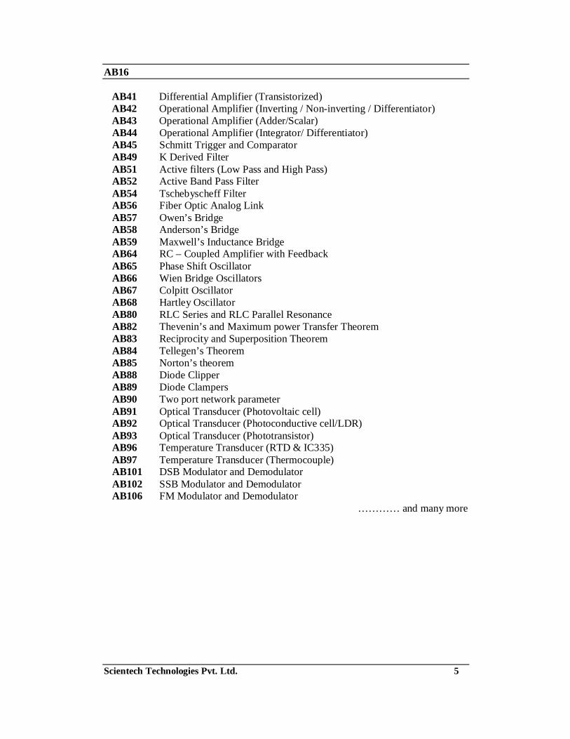
AB41 Differential Amplifier (Transistorized) AB42 Operational Amplifier (Inverting / Non-inverting / Differentiator) AB43 Operational Amplifier (Adder/Scalar) AB44 Operational Amplifier (Integrator/ Differentiator) AB45 Schmitt Trigger and Comparator AB49 K Derived Filter AB51 Active filters (Low Pass and High Pass) AB52 Active Band Pass Filter AB54 Tschebyscheff Filter AB56 Fiber Optic Analog Link AB57 Owen’s Bridge AB58 Anderson’s Bridge AB59 Maxwell’s Inductance Bridge AB64 RC – Coupled Amplifier with Feedback AB65 Phase Shift Oscillator AB66 Wien Bridge Oscillators AB67 Colpitt Oscillator AB68 Hartley Oscillator AB80 RLC Series and RLC Parallel Resonance AB82 Thevenin’s and Maximum power Transfer Theorem AB83 Reciprocity and Superposition Theorem AB84 Tellegen’s Theorem AB85 Norton’s theorem AB88 Diode Clipper AB89 Diode Clampers AB90 Two port network parameter AB91 Optical Transducer (Photovoltaic cell) AB92 Optical Transducer (Photoconductive cell/LDR) AB93 Optical Transducer (Phototransistor) AB96 Temperature Transducer (RTD & IC335) AB97 Temperature Transducer (Thermocouple) AB101 DSB Modulator and Demodulator AB102 SSB Modulator and Demodulator AB106 FM Modulator and Demodulator
………… and many more

AB16
Scientech Technologies Pvt. Ltd. 6
Theory Amplification is the process of increasing the strength of signal. An Amplifier is a device that provides amplification (the increase in current, voltage or power of signal) without appreciably altering the original signal.
A Bipolar transistor is frequently used as an amplifier. A bipolar transistor is a current amplifier, having three terminals Emitter, Base, Collector. A small current into base controls a large current flow from the collector to emitter. The large current flow is independent of voltage across the transistor from collector to emitter. This makes it possible to obtain a large amplification of voltage by taking the output voltage from a resistor in series with the collector.
Transistor can be used as an Amplifier in three configurations: 1. Common Base
2. Common Emitter 3. Common Collector
Common Collector Configuration : In this arrangement, the input signal is applied between base and collector and the output is taken from the emitter and collector. In this arrangement input current is base current and output current is emitter current.
Figure 1

AB16
Scientech Technologies Pvt. Ltd. 7
Current relations in CC configurations IE = IC + IB
IE = γ * IB + γ * ICBO
γ = IE / IB Where IB = Base current (input current) IC = Collector current IE = Emitter current (output current) ICEO = current through collector to emitter when base is open. γ = current amplification in CC configuration.
Operation of Common Collector amplifier : In order to get faithful amplification, the transistor is properly DC biased. The purpose of DC biasing is to obtain a certain DC Emitter current (IC) at a certain DC Emitter voltage (VEC). These values of current and voltage are called operating point (Quiescent point). To obtain DC operating point some biasing methods are used called biasing circuits. These biasing arrangements should be such as to operate the transistor in Active region. The Most commonly used Biasing circuits is voltage divider method. In this method two resistances R1 and R2 are connected across the supply voltage VCC and provide proper biasing. A voltage divider formed by R1 and R2, and the voltage drop across R2 Forward biased the base emitter junction causes the base current and hence collector current flows in zero signal condition. Resistance RE provides stabilization.
V2 = VCC * R2 / (R1 + R2) V2 = VBE + VE
V2 = VBE + IER IE = (V2 - VBE) / RE
IE is approximately equal to IC. IC = (V2 - VBE) / RE
VCE = VCC - IC (RC + RE)

AB16
Scientech Technologies Pvt. Ltd. 8
Figure 2
This method is widely used because operating point of transistor can be made almost independent of beta (β) and provides good stabilization of operating point. If this circuit is used to amplify AC voltages, some more components must be added to it. Coupling Capacitors (C1 &C3): They are used to pass AC input signal and block the DC voltage from the preceding circuit. This prevents DC in the circuitry on the left of coupling capacitor from affecting the bias on transistor. The coupling capacitor also blocks the bias of transistor from reaching the input signal source. It is also called blocking capacitor. Bypass Capacitors (C2): It bypasses all the AC current from the emitter to the ground. If the capacitor C2 is not put in the circuit, the AC voltage developed across RE will affect the input AC voltage, such a feedback is reduced by putting the capacitor C2.
RE: It represents the load resistance is connected at the output. In this amplifier input signal is injected into the base-collector circuit and output signal is taken out from the Emitter-Collector Circuit, When the output is taken from emitter terminal of transistor this network is referred as Emitter Follower or Common Collector Amplifier. In this amplifier output voltage is always less than the input signal, and output voltage is in phase with the input voltage. The fact that output voltage follows the magnitude of input voltage with an in-phase relationship accounts for the terminology "Emitter Follower".
When positive half cycle of the signal is applied then, 1. Forward biased is increased, since Vbe is positive w.r.t. collector i e. Ground.
2. Base current is increased, 3. Emitter current is increased,
4. Drop across Re is increased,

AB16
Scientech Technologies Pvt. Ltd. 9
5. Hence output voltage is increased; consequently positive half-cycle of the output is obtained. i.e. input and output are in phase with each other.
Figure 3
Operating Parameter of Common Collector Amplifier : Voltage Gain : The ratio or Output Voltage (Vo) to the input voltage (Vi) is known as voltage amplification or voltage gain of amplifier.
Voltage Gain (AV) = VO / Vi Input Impedance : It is the ratio of Input voltage (Vin) to Input current (Ii) Zin = Vin / Ii
To measure the input impedence a known resistor (Rs) is placed in series before the input coupling capacitor and the impedence could be calculated using the equation
Zin = Rs / (Av/Av`- l) Where Av = voltage gain without the resistor (Rs) Av` = voltage gain with the resistor (Rs)
Figure 4
Output Impedence : It is the ratio of Output voltage (Vout) to Output Current (Io). Zout = Vout / Io
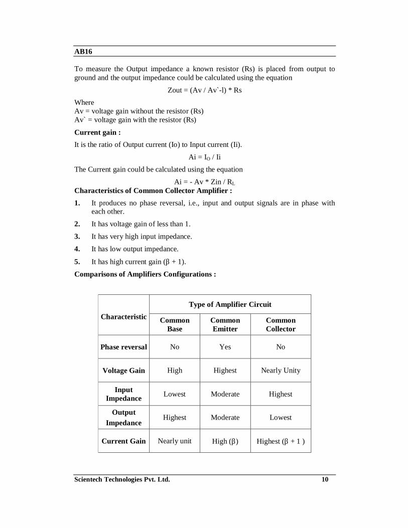
AB16
Scientech Technologies Pvt. Ltd. 10
To measure the Output impedance a known resistor (Rs) is placed from output to ground and the output impedance could be calculated using the equation
Zout = (Av / Av`-l) * Rs Where Av = voltage gain without the resistor (Rs) Av` = voltage gain with the resistor (Rs)
Current gain : It is the ratio of Output current (Io) to Input current (Ii).
Ai = IO / Ii The Current gain could be calculated using the equation
Ai = - Av * Zin / RL Characteristics of Common Collector Amplifier : 1. It produces no phase reversal, i.e., input and output signals are in phase with
each other.
2. It has voltage gain of less than 1.
3. It has very high input impedance.
4. It has low output impedance.
5. It has high current gain (β + 1).
Comparisons of Amplifiers Configurations :
Type of Amplifier Circuit Characteristic Common
Base Common Emitter
Common Collector
Phase reversal No Yes No
Voltage Gain High Highest Nearly Unity
Input Impedance Lowest Moderate Highest
Output Impedance
Highest Moderate Lowest
Current Gain Nearly unit High (β) Highest (β + 1 )

AB16
Scientech Technologies Pvt. Ltd. 11
Experiment Objective : Study the Common Collector Amplifier and to evaluate –Operating Point, Voltage gain (AV), input and output impedance, current gain of amplifier. Equipments Needed : 1. Analog board of AB16. 2. DC power supply +12V external source or ST2612 Analog Lab. 3. Digital Multimeter
4. 2 mm patch cords
Circuit diagram : Circuit used to study Common Collector Amplifier is shown in figure 5.
Figure 5

AB16
Scientech Technologies Pvt. Ltd. 12
Procedure : 1. Connect test point 2 and test point 3, test point 4 and test point 5, test point 6
and test point 7, using 2mm patch cords. 2. Connect +12V DC power supply at their indicated position from external source
or ST2612 Analog Lab.
3. Switch ‘On’ the power supply.
4. For the measurement of Quiescent Point measure the VEC by connecting voltmeter between test point 4 and test point 6. Measure Emitter current (IE) by connecting ammeter between test point 6 and test point 7.
5. Connect a sinusoidal signal of 10mV (p-p) at 25 KHz frequency at the Test point 1 (Input of amplifier).
6. Observe the amplified output on oscilloscope by connecting test point 8 (output of amplifier) to oscilloscope.
7. Calculate Voltage gain of amplifier. Connect Load resistor of 1K ohms at the output and find the voltage gain of amplifier with load resistor.
8. Calculate input impedance, output impedance, and current gain of amplifier using the mentioned formulas with resistance 1 K.
Result : Operating Point of the Common Collector Amplifier IC = ________ mA
VEC = _________V Voltage gain of the amplifier AV _________ =
Input impedance of amplifier Zin _________ = Output Impedance of amplifier Zout _______ =
Current gain of amplifier Ai = ____________

AB16
Scientech Technologies Pvt. Ltd. 13
Data Sheet

AB16
Scientech Technologies Pvt. Ltd. 14
AB16
Scientech Technologies Pvt. Ltd. 15
Warranty 1. We guarantee the product against all manufacturing defects for 24 months from
the date of sale by us or through our dealers. Consumables like dry cell etc. are not covered under warranty.
2. The guarantee will become void, if
a) The product is not operated as per the instruction given in the operating manual.
b) The agreed payment terms and other conditions of sale are not followed.
c) The customer resells the instrument to another party. d) Any attempt is made to service and modify the instrument.
3. The non-working of the product is to be communicated to us immediately giving full details of the complaints and defects noticed specifically mentioning the type, serial number of the product and date of purchase etc.
4. The repair work will be carried out, provided the product is dispatched securely packed and insured. The transportation charges shall be borne by the customer.
For any Technical Problem Please Contact us at [email protected]
List of Accessories
1. 2mm Patch Cord (Red) 16” .....................................................................1 No. 2. 2mm Patch Cord (Black) 16”................................................................. 3 Nos. 3. 2mm Patch Cord (Blue) 16” .................................................................. 5 Nos. 4. e-Manual.................................................................................................1 No.
Updated 26-06-2009