abc's of probes primer
TRANSCRIPT

Copyright © 1997 Tektronix, Inc. All rights reserved.
ABCs of Probes
Primer
When making measurements on electrical or electronic systems or circuitry, personal safety isof paramount importance. Be sure that you understand the capabilities and limitations of themeasuring equipment that you’re using. Also, before making any measurements, become thor-oughly familiar with the system or circuitry that you will be measuring. Review all documen-tation and schematics for the system being measured, paying particular attention to the levelsand locations of voltages in the circuit and heeding any and all cautionary notations.
Additionally, be sure to review the following safety precautions to avoid personal injury andto prevent damage to the measuring equipment or the systems to which it is attached. Foradditional explanation of any of the following precautions, please refer to Appendix A:Explanation of Safety Precautions.
• Observe All Terminal Ratings
• Use Proper Grounding Procedures
• Connect and Disconnect Probes Properly
• Avoid Exposed Circuitry
• Avoid RF Burns While Handling Probes
• Do Not Operate Without Covers
• Do Not Operate in Wet/Damp Conditions
• Do Not Operate in an Explosive Atmosphere
• Do Not Operate with Suspected Failures
• Keep Probe Surfaces Clean and Dry
• Do Not Immerse Probes in Liquids
Safety Summary
Chapter 1: Probes – The Critical Link To Measurement Quality· · · · · · · · · · · · · · · · · · · · · · · · 1
What is a Probe? · · · · · · · · · · · · · · · · · · · · · · · · · · · · · · · · · · · · · · · · · · · · · · · · · · · · · · · · · · · · · · 1
The Ideal Probe · · · · · · · · · · · · · · · · · · · · · · · · · · · · · · · · · · · · · · · · · · · · · · · · · · · · · · · · · · · · · · · 2
The Realities of Probes · · · · · · · · · · · · · · · · · · · · · · · · · · · · · · · · · · · · · · · · · · · · · · · · · · · · · · · · · 4
Choosing the Right Probe · · · · · · · · · · · · · · · · · · · · · · · · · · · · · · · · · · · · · · · · · · · · · · · · · · · · · · · 8
Some Probing Tips · · · · · · · · · · · · · · · · · · · · · · · · · · · · · · · · · · · · · · · · · · · · · · · · · · · · · · · · · · · · 8
Summary · · · · · · · · · · · · · · · · · · · · · · · · · · · · · · · · · · · · · · · · · · · · · · · · · · · · · · · · · · · · · · · · · · · 10
Chapter 2: Different Probes for Different Needs · · · · · · · · · · · · · · · · · · · · · · · · · · · · · · · · · · · · 11
Why So Many Probes? · · · · · · · · · · · · · · · · · · · · · · · · · · · · · · · · · · · · · · · · · · · · · · · · · · · · · · · · 11
Different Probe Types and Their Benefits · · · · · · · · · · · · · · · · · · · · · · · · · · · · · · · · · · · · · · · · · 13
Floating Measurements · · · · · · · · · · · · · · · · · · · · · · · · · · · · · · · · · · · · · · · · · · · · · · · · · · · · · · · 18
Probe Accessories · · · · · · · · · · · · · · · · · · · · · · · · · · · · · · · · · · · · · · · · · · · · · · · · · · · · · · · · · · · · 20
Chapter 3: How Probes Affect Your Measurements · · · · · · · · · · · · · · · · · · · · · · · · · · · · · · · · · 23
The Effect of Source Impedance · · · · · · · · · · · · · · · · · · · · · · · · · · · · · · · · · · · · · · · · · · · · · · · · 23
Capacitive Loading · · · · · · · · · · · · · · · · · · · · · · · · · · · · · · · · · · · · · · · · · · · · · · · · · · · · · · · · · · · 23
Bandwidth Considerations · · · · · · · · · · · · · · · · · · · · · · · · · · · · · · · · · · · · · · · · · · · · · · · · · · · · · 25
What To Do About Probing Effects · · · · · · · · · · · · · · · · · · · · · · · · · · · · · · · · · · · · · · · · · · · · · · 29
Chapter 4: Understanding Probe Specifications · · · · · · · · · · · · · · · · · · · · · · · · · · · · · · · · · · · 31
Aberrations (universal) · · · · · · · · · · · · · · · · · · · · · · · · · · · · · · · · · · · · · · · · · · · · · · · · · · · · · · · · 31
Amp-Second Product (current probes) · · · · · · · · · · · · · · · · · · · · · · · · · · · · · · · · · · · · · · · · · · · 31
Attenuation Factor (universal · · · · · · · · · · · · · · · · · · · · · · · · · · · · · · · · · · · · · · · · · · · · · · · · · · 31
Accuracy (universal) · · · · · · · · · · · · · · · · · · · · · · · · · · · · · · · · · · · · · · · · · · · · · · · · · · · · · · · · · · 31
Bandwidth (universal) · · · · · · · · · · · · · · · · · · · · · · · · · · · · · · · · · · · · · · · · · · · · · · · · · · · · · · · · 32
Capacitance (universal) · · · · · · · · · · · · · · · · · · · · · · · · · · · · · · · · · · · · · · · · · · · · · · · · · · · · · · · 32
CMRR (differential probes) · · · · · · · · · · · · · · · · · · · · · · · · · · · · · · · · · · · · · · · · · · · · · · · · · · · · · 32
CW Frequency Current Derating (current probes) · · · · · · · · · · · · · · · · · · · · · · · · · · · · · · · · · · · 33
Decay Time Constant (current probes) · · · · · · · · · · · · · · · · · · · · · · · · · · · · · · · · · · · · · · · · · · · 33
Direct Current (current probes) · · · · · · · · · · · · · · · · · · · · · · · · · · · · · · · · · · · · · · · · · · · · · · · · · 33
Insertion Impedance (current probes) · · · · · · · · · · · · · · · · · · · · · · · · · · · · · · · · · · · · · · · · · · · · 33
Input Capacitance (universal) · · · · · · · · · · · · · · · · · · · · · · · · · · · · · · · · · · · · · · · · · · · · · · · · · · 33
Input Resistance (universal) · · · · · · · · · · · · · · · · · · · · · · · · · · · · · · · · · · · · · · · · · · · · · · · · · · · · 33
Maximum Input Current Rating (current probes) · · · · · · · · · · · · · · · · · · · · · · · · · · · · · · · · · · · 33
Maximum Peak Pulse Current Rating (current probes) · · · · · · · · · · · · · · · · · · · · · · · · · · · · · · · 33
Maximum Voltage Rating (universal) · · · · · · · · · · · · · · · · · · · · · · · · · · · · · · · · · · · · · · · · · · · · 33
Propagation Delay (universal) · · · · · · · · · · · · · · · · · · · · · · · · · · · · · · · · · · · · · · · · · · · · · · · · · · 33
Rise Time (universal) · · · · · · · · · · · · · · · · · · · · · · · · · · · · · · · · · · · · · · · · · · · · · · · · · · · · · · · · · 34
Tangential Noise (active probes) · · · · · · · · · · · · · · · · · · · · · · · · · · · · · · · · · · · · · · · · · · · · · · · · 34
Temperature Range (universal) · · · · · · · · · · · · · · · · · · · · · · · · · · · · · · · · · · · · · · · · · · · · · · · · · 34
Chapter 5: A Guide to Probe Selection · · · · · · · · · · · · · · · · · · · · · · · · · · · · · · · · · · · · · · · · · · · 35
Understanding the Signal Source · · · · · · · · · · · · · · · · · · · · · · · · · · · · · · · · · · · · · · · · · · · · · · · 35
Oscilloscope Issues · · · · · · · · · · · · · · · · · · · · · · · · · · · · · · · · · · · · · · · · · · · · · · · · · · · · · · · · · · · 37
Selecting the Right Probe · · · · · · · · · · · · · · · · · · · · · · · · · · · · · · · · · · · · · · · · · · · · · · · · · · · · · · 38
Chapter 6: Advanced Probing Techniques · · · · · · · · · · · · · · · · · · · · · · · · · · · · · · · · · · · · · · · · 39
Ground Lead Issues · · · · · · · · · · · · · · · · · · · · · · · · · · · · · · · · · · · · · · · · · · · · · · · · · · · · · · · · · · 39
Differential Measurements · · · · · · · · · · · · · · · · · · · · · · · · · · · · · · · · · · · · · · · · · · · · · · · · · · · · · 42
Small Signal Measurements · · · · · · · · · · · · · · · · · · · · · · · · · · · · · · · · · · · · · · · · · · · · · · · · · · · · 45
page i
Table of Contents
Appendix A: Explanation of Safety Precautions · · · · · · · · · · · · · · · · · · · · · · · · · · · · · · · · · · · 49
Observe All Terminal Ratings · · · · · · · · · · · · · · · · · · · · · · · · · · · · · · · · · · · · · · · · · · · · · · · · · · 49
Use Proper Grounding Procedures · · · · · · · · · · · · · · · · · · · · · · · · · · · · · · · · · · · · · · · · · · · · · · · 49
Connect and Disconnect Probes Properly · · · · · · · · · · · · · · · · · · · · · · · · · · · · · · · · · · · · · · · · · 49
Avoid Exposed Circuitry · · · · · · · · · · · · · · · · · · · · · · · · · · · · · · · · · · · · · · · · · · · · · · · · · · · · · · 50
Avoid RF Burns While Handling Probes · · · · · · · · · · · · · · · · · · · · · · · · · · · · · · · · · · · · · · · · · · 50
Do Not Operate Without Covers · · · · · · · · · · · · · · · · · · · · · · · · · · · · · · · · · · · · · · · · · · · · · · · · · 50
Do Not Operate in Wet/Damp Conditions · · · · · · · · · · · · · · · · · · · · · · · · · · · · · · · · · · · · · · · · · 50
Do Not Operate in an Explosive Atmosphere · · · · · · · · · · · · · · · · · · · · · · · · · · · · · · · · · · · · · · 50
Do Not Operate with Suspected Failures · · · · · · · · · · · · · · · · · · · · · · · · · · · · · · · · · · · · · · · · · 50
Keep Probe Surfaces Clean and Dry · · · · · · · · · · · · · · · · · · · · · · · · · · · · · · · · · · · · · · · · · · · · · · 50
Do Not Immerse Probes in Liquids · · · · · · · · · · · · · · · · · · · · · · · · · · · · · · · · · · · · · · · · · · · · · · 50
Appendix B: Glossary · · · · · · · · · · · · · · · · · · · · · · · · · · · · · · · · · · · · · · · · · · · · · · · · · · · · · · · · 51
page ii

page 1
probe as the oscilloscope.Weaken that first link with aninadequate probe or poorprobing methods, and theentire chain is weakened.
In this and following chap-ters, you’ll learn what con-tributes to the strengths andweaknesses of probes andhow to select the right probefor your application. You’llalso learn some important tipsfor using probes properly.
What Is a Probe?As a first step, let’s establishwhat an oscilloscope probe is.
Basically, a probe makes aphysical and electrical con-nection between a test pointor signal source and an oscil-loscope. Depending on yourmeasurement needs, this con-
nection can be made withsomething as simple as alength of wire or with some-thing as sophisticated as anactive differential probe.
At this point, it’s enough tosay that an oscilloscope probeis some sort of device or net-work that connects the signalsource to the input of theoscilloscope. This is illus-trated in Figure 1-1, wherethe probe is indicated as anundefined box in the mea-surement diagram.
Whatever the probe is in real-ity, it must provide a connec-tion of adequate convenienceand quality between the sig-nal source and the scopeinput (Figure 1-2). The ade-quacy of connection has threekey defining issues – physical
Probes are vital to oscillo-scope measurements. Tounderstand how vital, discon-nect the probes from an oscil-loscope and try to make ameasurement. It can’t bedone. There has to be somekind of electrical connection,a probe of some sort betweenthe signal to be measured andthe oscilloscope’s inputchannel.
In addition to being vital tooscilloscope measurements,probes are also critical tomeasurement quality. Con-necting a probe to a circuitcan affect the operation of thecircuit, and an oscilloscopecan only display and measurethe signal that the probedelivers to the scope input.Thus, it is imperative that theprobe have minimum impacton the probed circuit and thatit maintain adequate signalfidelity for the desired mea-surements.
If the probe doesn’t maintainsignal fidelity, if it changesthe signal in any way orchanges the way a circuitoperates, the scope sees a dis-torted version of the actualsignal. The result can bewrong or misleading mea-surements.
In essence, the probe is thefirst link in the oscilloscopemeasurement chain. And thestrength of this measurementchain relies as much on the
Figure 1-1. A probe is a device that makes a physical and electrical connec-tion between the oscilloscope and test point.
Figure 1-2. Most probes consist of a probe head, a probe cable, and a com-pensation box or other signal conditioning network.
Chapter 1: Probes – The Critical Link to Measurement Quality

page 2
attachment, impact on circuitoperation, and signal trans-m i s s i o n .
To make an oscilloscope mea-surement, you must first beable to physically get theprobe to the test point. Tomake this possible, mostprobes have at least a meteror two of cable associatedwith them, as indicated inFigure 1-2. This probe cableallows the oscilloscope to beleft in a stationary position ona cart or bench top while theprobe is moved from testpoint to test point in the cir-cuit being tested. There is atradeoff for this convenience,though. The probe cablereduces the probe’s band-width; the longer the cable,the greater the reduction.
In addition to the length ofcable, most probes also havea probe head, or handle, witha probe tip. The probe headallows you to hold the probewhile you maneuver the tipto make contact with the testpoint. Often, this probe tip isin the form of a spring-loadedhook that allows you to actu-ally attach the probe to thetest point.
Physically attaching theprobe to the test point alsoestablishes an electrical con-nection between the probetip and the oscilloscopeinput. For useable measure-ment results, attaching theprobe to a circuit must haveminimum affect on the waythe circuit operates, and thesignal at the probe tip mustbe transmitted with adequatefidelity through the probehead and cable to the oscillo-scope’s input.
These three issues – physicalattachment, minimum impacton circuit operation, and ade-quate signal fidelity – encom-pass most of what goes intoproper selection of a probe.Because probing effects andsignal fidelity are the morecomplex topics, much of thisprimer is devoted to thoseissues. However, the issue ofphysical connection shouldnever be ignored. Difficultyin connecting a probe to a
test point often leads to prob-ing practices that reducefidelity.
The Ideal ProbeIn an ideal world, the idealprobe would offer the follow-ing key attributes:
• Connection ease and conve-nience
• Absolute signal fidelity• Zero signal source loading• Complete noise immunity
Connection ease and conve-nience. Making a physicalconnection to the test pointhas already been mentionedas one of the key require-ments of probing. With theideal probe, you should alsobe able to make the physicalconnection with both easeand convenience.
For miniaturized circuitry,such as high-density surfacemount technology (SMT),connection ease and conve-nience are promoted throughsubminiature probe headsand various probe-tipadapters designed for SMTdevices. Such a probing sys-tem is shown in Figure 1-3a.These probes, however, aretoo small for practical use inapplications such as indus-trial power circuitry wherehigh voltages and largergauge wires are common. Forpower applications, physi-cally larger probes withgreater margins of safety arerequired. Figures 1-3b and1-3c show examples of suchprobes, where Figure 1-3b is ahigh-voltage probe and Figure1-3c is a clamp-on currentprobe.
From these few examples ofphysical connection, it’s clearthat there’s no single idealprobe size or configurationfor all applications. Becauseof this, various probe sizesand configurations have beendesigned to meet the physicalconnection requirements ofvarious applications.
Absolute signal fidelity. Theideal probe should transmitany signal from probe tip toscope input with absolute sig-nal fidelity. In other words,the signal as it occurs at the
Figure 1-3. Various probes are available for different applicationtechnologies and measurement needs.
a. Probing SMT devices.
b. High-voltage probe.
c. Clamp-on Current probe.
NEW TERMSbandwidth – The continuous bandof frequencies that a network or cir-cuit passes without diminishingpower more than 3 dB from themidband power (refer to Figure 1-5).
loading – The process whereby aload applied to a source draws cur-rent from the source.

page 3
the probe must have infiniteimpedance, essentially pre-senting an open circuit to thetest point.
In practice, a probe with zerosignal source loading cannotbe achieved. This is because aprobe must draw some smallamount of signal current inorder to develop a signal volt-age at the oscilloscope input.Consequently, some signalsource loading is to beexpected when using a probe.The goal, however, shouldalways be to minimize theamount of loading throughappropriate probe selection.
Complete noise immunity.Fluorescent lights and fanmotors are just two of themany electrical noise sourcesin our environment. Thesesources can induce theirnoise onto nearby electricalcables and circuitry, causingthe noise to be added to sig-nals. Because of susceptibil-ity to induced noise, a simplepiece of wire is a less thanideal choice for an oscillo-scope probe.
The ideal oscilloscope probeis completely immune to allnoise sources. As a result, thesignal delivered to the oscil-loscope has no more noise onit than what appeared on thesignal at the test point.
In practice, use of shieldingallows probes to achieve ahigh level of noise immunityfor most common signal lev-els. Noise, however, can stillbe a problem for certain low-level signals. In particular,common mode noise can pre-sent a problem for differentialmeasurements, as will be dis-cussed later.
probe tip should be faithfullyduplicated at the scopeinput.
For absolute fidelity, theprobe circuitry from tip toscope input must have zeroattenuation, infinite band-width, and linear phaseacross all frequencies. Notonly are these ideal require-ments impossible to achievein reality, but they areimpractical. For example,there’s no need for an infinitebandwidth probe, or oscillo-scope for that matter, whenyou’re dealing with audio fre-quency signals. Nor is there aneed for infinite bandwidthwhen 500 MHz will do forcovering most high-speeddigital, TV, and other typicaloscilloscope applications.
Still, within a given band-width of operation, absolutesignal fidelity is an ideal tobe sought after.
Zero signal source loading.The circuitry behind a testpoint can be thought of as ormodeled as a signal source.Any external device, such asa probe, that’s attached to thetest point can appear as anadditional load on the signalsource behind the test point.
The external device acts as aload when it draws signalcurrent from the circuit (thesignal source). This loading,or signal current draw,changes the operation of thecircuitry behind the testpoint, and thus changes thesignal seen at the test point.
An ideal probe causes zerosignal source loading. Inother words, it doesn’t drawany signal current from thesignal source. This meansthat, for zero current draw,
NEW TERMSattenuation – The process wherebythe amplitude of a signal is reduced.
phase – A means of expressing thetime-related positions of waveformsor waveform components relative toa reference point or waveform. Forexample, a cosine wave by defini-tion has zero phase, and a sine waveis a cosine wave with 90-degrees ofphase shift.
linear phase – The characteristic ofa network whereby the phase of anapplied sine wave is shifted linearlywith increasing sine wave fre-quency; a network with linear phaseshift maintains the relative phaserelationships of harmonics in non-sinusoidal waveforms so that there’sno phase-related distortion in thewaveform.
load – The impedance that’s placedacross a signal source; an open cir-cuit would be a “no load” situation.
impedance – The process of imped-ing or restricting AC signal flow.Impedance is expressed in Ohmsand consists of a resistive compo-nent (R) and a reactive component(X) that can be either capacitive (XC)or inductive (XL). Impedance (Z) isexpressed in a complex form as:
Z = R + jX
or as a magnitude and phase, wherethe magnitude (M) is:
M = R2 + X2
and phase θ is:θ = arctan(X/R)
shielding – The practice of placing agrounded conductive sheet of mate-rial between a circuit and externalnoise sources so that the shieldingmaterial intercepts noise signalsand conducts them away from thecircuit.
page 4
with some series resistanceand a terminating resistance(Figure 1-4a). However, forAC signals, the picturechanges dramatically as sig-nal frequencies increase (Fig-ure 1-4b).
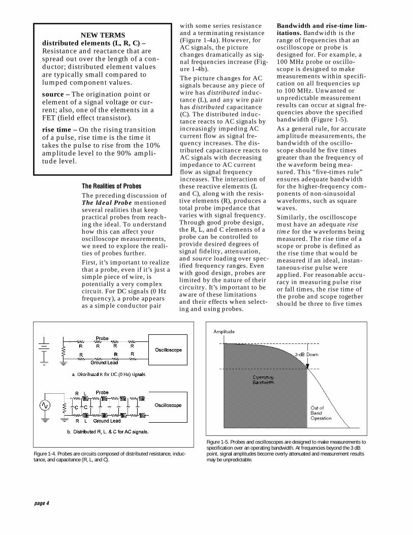
The picture changes for ACsignals because any piece ofwire has distributed induc-tance (L), and any wire pairhas distributed capacitance(C). The distributed induc-tance reacts to AC signals byincreasingly impeding ACcurrent flow as signal fre-quency increases. The dis-tributed capacitance reacts toAC signals with decreasingimpedance to AC currentflow as signal frequencyincreases. The interaction ofthese reactive elements (Land C), along with the resis-tive elements (R), produces atotal probe impedance thatvaries with signal frequency.Through good probe design,the R, L, and C elements of aprobe can be controlled toprovide desired degrees ofsignal fidelity, attenuation,and source loading over spec-ified frequency ranges. Evenwith good design, probes arelimited by the nature of theircircuitry. It’s important to beaware of these limitationsand their effects when select-ing and using probes.
Bandwidth and rise-time lim-itations. Bandwidth is therange of frequencies that anoscilloscope or probe isdesigned for. For example, a100 MHz probe or oscillo-scope is designed to makemeasurements within specifi-cation on all frequencies upto 100 MHz. Unwanted orunpredictable measurementresults can occur at signal fre-quencies above the specifiedbandwidth (Figure 1-5).
As a general rule, for accurateamplitude measurements, thebandwidth of the oscillo-scope should be five timesgreater than the frequency ofthe waveform being mea-sured. This “five-times rule”ensures adequate bandwidthfor the higher-frequency com-ponents of non-sinusoidalwaveforms, such as squarewaves.
Similarly, the oscilloscopemust have an adequate risetime for the waveforms beingmeasured. The rise time of ascope or probe is defined asthe rise time that would bemeasured if an ideal, instan-taneous-rise pulse wereapplied. For reasonable accu-racy in measuring pulse riseor fall times, the rise time ofthe probe and scope togethershould be three to five times
The Realities of ProbesThe preceding discussion ofThe Ideal Probe mentionedseveral realities that keeppractical probes from reach-ing the ideal. To understandhow this can affect youroscilloscope measurements,we need to explore the reali-ties of probes further.
First, it’s important to realizethat a probe, even if it’s just asimple piece of wire, ispotentially a very complexcircuit. For DC signals (0 Hzfrequency), a probe appearsas a simple conductor pair
Figure 1-4. Probes are circuits composed of distributed resistance, induc-tance, and capacitance (R, L, and C).
Figure 1-5. Probes and oscilloscopes are designed to make measurements tospecification over an operating bandwidth. At frequencies beyond the 3 dBpoint, signal amplitudes become overly attenuated and measurement resultsmay be unpredictable.
NEW TERMSdistributed elements (L, R, C) –Resistance and reactance that arespread out over the length of a con-ductor; distributed element valuesare typically small compared tolumped component values.
so u rce – The origination point orelement of a signal voltage or cur-rent; also, one of the elements in aFET (field effect transistor).
rise time – On the rising transitionof a pulse, rise time is the time ittakes the pulse to rise from the 10%amplitude level to the 90% ampli-tude level.

page 5
has its own set of bandwidthand rise-time limits. And,when a probe is attached to anoscilloscope, you get a new setof system bandwidth and rise-time limits.
Unfortunately, the relation-ship between system band-width and the individualscope and probe bandwidthsis not a simple one. The sameis true for rise times. To copewith this, manufacturers ofquality oscilloscopes specifybandwidth or rise time to theprobe tip when the scope isused with specific probemodels. This is importantbecause the oscilloscope andprobe together form a mea-surement system, and it’s thebandwidth and rise time ofthe system that determine itsmeasurement capabilities. Ifyou use a probe that is not onthe scope’s recommended listof probes, you run the risk ofunpredictable measurementresults.
Dynamic range limitations.All probes have a high-volt-age safety limit that shouldnot be exceeded. For passiveprobes, this limit can rangefrom hundreds of volts tothousands of volts. However,for active probes, the maxi-mum safe voltage limit isoften in the range of tens ofvolts. To avoid personalsafety hazards as well aspotential damage to theprobe, it’s wise to be aware ofthe voltages being measuredand the voltage limits of theprobes being used.
In addition to safety consid-erations, there’s also thepractical consideration ofmeasurement dynamic range.Oscilloscopes have ampli-
tude sensitivity ranges. Forexample, 1 mV to 10 V/divi-sion is a typical sensitivityrange. On an eight-divisiondisplay, this means that youcan typically make reason-ably accurate measurementson signals ranging from 4 mVpeak-to-peak to 40 V peak-to-peak. This assumes, at mini-mum, a four-division ampli-tude display of the signal toobtain reasonable measure-ment resolution.
With a 1X probe (1-timesprobe), the dynamic measure-ment range is the same as thatof the oscilloscope. For theexample above, this would bea signal measurement rangeof 4 mV to 40 V.
But, what if you need to mea-sure a signal beyond the 40 Vrange?
You can shift the scope’sdynamic range to higher volt-ages by using an attenuatingprobe. A 10X probe, forexample, shifts the dynamicrange to 40 mV to 400 V. Itdoes this by attenuating theinput signal by a factor of 10,which effectively multipliesthe scope’s scaling by 10.
For most general-purposeuse, 10X probes are preferred,both because of their high-end voltage range andbecause they cause less signalsource loading. However, ifyou plan to measure a verywide range of voltage levels,you may want to consider aswitchable 1X/10X probe.This gives you a dynamicrange of 4 mV to 400 V. How-ever, in the 1X mode, morecare must be taken withregard to signal sourceloading.
faster than that of the pulsebeing measured (Figure 1-6).
In cases where rise time isn’tspecified, you can derive risetime (Tr) from the bandwidth(BW) specification with thefollowing relationship:
Tr = 0.35/BW
Every oscilloscope has definedbandwidth and rise-time lim-its. Similarly, every probe also
Figure 1-6. Rise time measurement error can be estimated fromthe above chart. A scope/probe combination with a rise time threetimes faster than the pulse being measured (3:1 ratio) can beexpected to measure the pulse rise time to within 5%. A 5:1 ratiowould result in only 2% error.
NEW TERMSactive probe – A probe containingtransistors or other active devices aspart of the probe’s signal condition-ing network.
passive probe – A probe whose net-work equivalent consists only ofresistive (R), inductive (L), or capac-itive (C) elements; a probe that con-tains no active components.

page 6
Source loading. As previ-ously mentioned, a probemust draw some signal cur-rent in order to develop a sig-nal voltage at the scopeinput. This places a load atthe test point that can changethe signal that the circuit, orsignal source, delivers to thetest point.
The simplest example ofsource loading effects is toconsider measurement of abattery-driven resistive net-work. This is shown in Figure1-7. In Figure 1-7a, before aprobe is attached, the battery’sDC voltage is divided acrossthe battery’s internal resis-tance (Ri) and the load resis-tance (Rl) that the battery isdriving. For the values givenin the diagram, this results inan output voltage of:
Eo = Eb * Rl/ ( R i + Rl)
= 100 V * 1 0 0 , 0 0 0 /(100 + 100,000)
= 10,000,000 V/100,100
= 99.9 V
In Figure 1-7b, a probe hasbeen attached to the circuit,placing the probe resistance(Rp) in parallel with Rl. If Rpis 100 kΩ, the effective loadresistance in Figure 1-7b iscut in half to 50 kΩ. Theloading effect of this on Eo is:
Eo = 1 0 0 V * 5 0 , 0 0 0 /(100 + 50,000)
= 5,000,000 V / 5 0 , 1 0 0
= 99.8 V
This loading effect of 99.9versus 99.8 is only 0.1% andis negligible for most pur-poses. However, if Rp w e r esmaller, say 10 kΩ, the effectwould no longer be negligible.
To minimize such resistiveloading, 1X probes typicallyhave a resistance of 1 MΩ,and 10X probes typicallyhave a resistance of 10 MΩ.For most cases, these valuesresult in virtually no resistiveloading. Some loading shouldbe expected, though, whenmeasuring high-resistancesources.
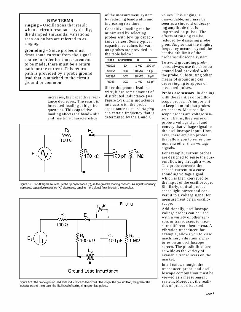
Usually, the loading of great-est concern is that caused bythe capacitance at the probetip (see Figure 1-8). For lowfrequencies, this capacitancehas a reactance that is veryhigh, and there’s little or noeffect. But, as frequency
NEW TERMreactance – An impedance elementthat reacts to an AC signal byrestricting its current flow based onthe signal’s frequency. A capacitor(C) presents a capacitive reactanceto AC signals that is expressed inOhms by the following relationship:
XC = 12πfC
where:XC = capacitive reactance in
Ohmsπ = 3.14159...f = frequency in HzC = capacitance in Farads
An inductor (L) presents an induc-tive reactance to AC signals that’sexpressed in Ohms by the followingrelationship:
XL = 2πfL
where:XL = inductive reactance in Ohmsπ = 3.14159....f = frequency in HzL = inductance in Henrys
Figure 1-7. An example of resistive loading.
page 7
of the measurement systemby reducing bandwidth andincreasing rise time.
Capacitive loading can beminimized by selectingprobes with low tip capaci-tance values. Some typicalcapacitance values for vari-ous probes are provided inthe table below:
Probe Attenuation R C
P6101B 1X 1 MΩ 100 pF
P6106A 10X 10 MΩ 11 pF
P6139A 10X 10 MΩ 8 pF
P6243 10X 1 MΩ ≤1 pF
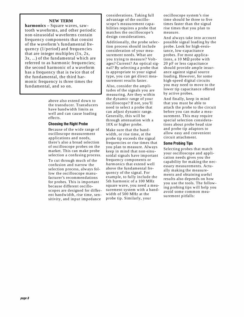
Since the ground lead is awire, it has some amount ofdistributed inductance (seeFigure 1-9). This inductanceinteracts with the probecapacitance to cause ringingat a certain frequency that isdetermined by the L and C
values. This ringing isunavoidable, and may beseen as a sinusoid of decay-ing amplitude that isimpressed on pulses. Theeffects of ringing can bereduced by designing probegrounding so that the ringingfrequency occurs beyond thebandwidth limit of theprobe/oscilloscope system.
To avoid grounding prob-lems, always use the shortestground lead provided withthe probe. Substituting othermeans of grounding cancause ringing to appear onmeasured pulses.
Probes are sensors. In dealingwith the realities of oscillo-scope probes, it’s importantto keep in mind that probesare sensors. Most oscillo-scope probes are voltage sen-sors. That is, they sense orprobe a voltage signal andconvey that voltage signal tothe oscilloscope input. How-ever, there are also probesthat allow you to sense phe-nomena other than voltagesignals.
For example, current probesare designed to sense the cur-rent flowing through a wire.The probe converts thesensed current to a corre-sponding voltage signalwhich is then conveyed tothe input of the oscilloscope.Similarly, optical probessense light power and con-vert it to a voltage signal formeasurement by an oscillo-scope.
Additionally, oscilloscopevoltage probes can be usedwith a variety of other sen-sors or transducers to mea-sure different phenomena. Avibration transducer, forexample, allows you to viewmachinery vibration signa-tures on an oscilloscopescreen. The possibilities areas wide as the variety ofavailable transducers on themarket.
In all cases, though, thetransducer, probe, and oscil-loscope combination must beviewed as a measurementsystem. Moreover, the reali-ties of probes discussed
increases, the capacitive reac-tance decreases. The result isincreased loading at high fre-quencies. This capacitiveloading affects the bandwidthand rise time characteristics
Figure 1-8. For ACsignal sources, probe tip capacitance (Cp) is the greatest loading concern. As signal frequencyincreases, capacitive reactance (Xc) decreases, causing more signal flow through the capacitor.
Figure 1-9. The probe ground lead adds inductance to the circuit. The longer the ground lead, the greater theinductance and the greater the likelihood of seeing ringing on fast pulses.
NEW TERMSringing – Oscillations that resultwhen a circuit resonates; typically,the damped sinusoidal variationsseen on pulses are referred to asringing.
grounding – Since probes mustdraw some current from the signalsource in order for a measurementto be made, there must be a returnpath for the current. This returnpath is provided by a probe groundlead that is attached to the circuitground or common.
page 8
considerations. Taking fulladvantage of the oscillo-scope’s measurement capa-bilities requires a probe thatmatches the oscilloscope’sdesign considerations.
Additionally, the probe selec-tion process should includeconsideration of your mea-surement needs. What areyou trying to measure? Volt-ages? Current? An optical sig-nal? By selecting a probe thatis appropriate to your signaltype, you can get direct mea-surement results faster.
Also, consider the ampli-tudes of the signals you aremeasuring. Are they withinthe dynamic range of youroscilloscope? If not, you’llneed to select a probe thatcan adjust dynamic range.Generally, this will bethrough attenuation with a10X or higher probe.
Make sure that the band-width, or rise time, at theprobe tip exceeds the signalfrequencies or rise times thatyou plan to measure. Alwayskeep in mind that non-sinu-soidal signals have importantfrequency components orharmonics that extend wellabove the fundamental fre-quency of the signal. Forexample, to fully include the5th harmonic of a 100 MHzsquare wave, you need a mea-surement system with a band-width of 500 MHz at theprobe tip. Similarly, your
oscilloscope system’s risetime should be three to fivetimes faster than the signalrise times that you plan tomeasure.
And always take into accountpossible signal loading by theprobe. Look for high-resis-tance, low-capacitanceprobes. For most applica-tions, a 10 MΩ probe with20 pF or less capacitanceshould provide ample insur-ance against signal sourceloading. However, for somehigh-speed digital circuitsyou may need to move to thelower tip capacitance offeredby active probes.
And finally, keep in mindthat you must be able toattach the probe to the circuitbefore you can make a mea-surement. This may requirespecial selection considera-tions about probe head sizeand probe tip adaptors toallow easy and convenientcircuit attachment.
Some Probing TipsSelecting probes that matchyour oscilloscope and appli-cation needs gives you thecapability for making the nec-essary measurements. Actu-ally making the measure-ments and obtaining usefulresults also depends on howyou use the tools. The follow-ing probing tips will help youavoid some common mea-surement pitfalls:
above also extend down tothe transducer. Transducershave bandwidth limits aswell and can cause loadingeffects.
Choosing the Right ProbeBecause of the wide range ofoscilloscope measurementapplications and needs,there’s also a broad selectionof oscilloscope probes on themarket. This can make probeselection a confusing process.
To cut through much of theconfusion and narrow theselection process, always fol-low the oscilloscope manu-facturer’s recommendationsfor probes. This is importantbecause different oscillo-scopes are designed for differ-ent bandwidth, rise time, sen-sitivity, and input impedance
NEW TERMharmonics – Square waves, saw-tooth waveforms, and other periodicnon-sinusoidal waveforms containfrequency components that consistof the waveform’s fundamental fre-quency (1/period) and frequenciesthat are integer multiples (1x, 2x,3x, ...) of the fundamental which arereferred to as harmonic frequencies;the second harmonic of a waveformhas a frequency that is twice that ofthe fundamental, the third har-monic frequency is three times thefundamental, and so on.
page 9
attenuating probes (10X and100X probes), have built-incompensation networks.
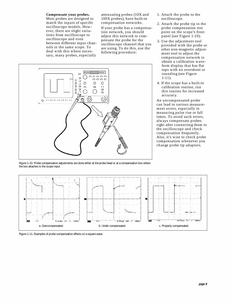
If your probe has a compensa-tion network, you shouldadjust this network to com-pensate the probe for theoscilloscope channel that youare using. To do this, use thefollowing procedure:
1. Attach the probe to theoscilloscope.
2. Attach the probe tip to theprobe compensation testpoint on the scope’s frontpanel (see Figure 1-10).
3. Use the adjustment toolprovided with the probe orother non-magnetic adjust-ment tool to adjust thecompensation network toobtain a calibration wave-form display that has flattops with no overshoot orrounding (see Figure1-11).
4. If the scope has a built-incalibration routine, runthis routine for increasedaccuracy.
An uncompensated probecan lead to various measure-ment errors, especially inmeasuring pulse rise or falltimes. To avoid such errors,always compensate probesright after connecting them tothe oscilloscope and checkcompensation frequently.Also, it’s wise to check probecompensation whenever youchange probe tip adaptors.
Compensate your probes.Most probes are designed tomatch the inputs of specificoscilloscope models. How-ever, there are slight varia-tions from oscilloscope tooscilloscope and evenbetween different input chan-nels in the same scope. Todeal with this where neces-sary, many probes, especially
Figure 1-11. Examples of probe compensation effects on a square wave.
Figure 1-10. Probe compensation adjustments are done either at the probe head or at a compensation box wherethe box attaches to the scope input.
a. Overcompensated. b. Under compensated. c. Properly compensated.
Use appropriate probe tipadapters whenever possible.A probe tip adapter that’sappropriate to the circuitbeing measured makes probeconnection quick, conve-nient, and electrically repeat-able and stable. Unfortu-nately, it’s not uncommon tosee short lengths of wire sol-dered to circuit points as asubstitute for a probe tipadapter.
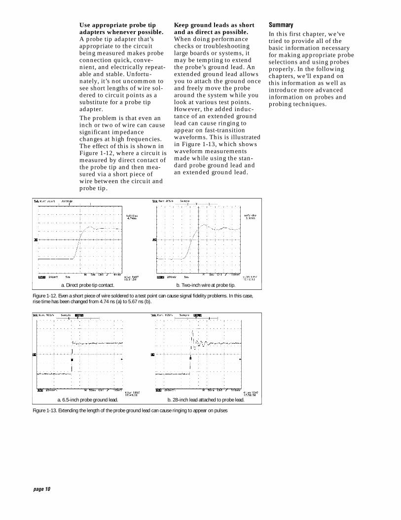
The problem is that even aninch or two of wire can causesignificant impedancechanges at high frequencies.The effect of this is shown inFigure 1-12, where a circuit ismeasured by direct contact ofthe probe tip and then mea-sured via a short piece ofwire between the circuit andprobe tip.
Keep ground leads as shortand as direct as possible.When doing performancechecks or troubleshootinglarge boards or systems, itmay be tempting to extendthe probe’s ground lead. Anextended ground lead allowsyou to attach the ground onceand freely move the probearound the system while youlook at various test points.However, the added induc-tance of an extended groundlead can cause ringing toappear on fast-transitionwaveforms. This is illustratedin Figure 1-13, which showswaveform measurementsmade while using the stan-dard probe ground lead andan extended ground lead.
SummaryIn this first chapter, we’vetried to provide all of thebasic information necessaryfor making appropriate probeselections and using probesproperly. In the followingchapters, we’ll expand onthis information as well asintroduce more advancedinformation on probes andprobing techniques.
page 10
Figure 1-12. Even a short piece of wire soldered to a test point can cause signal fidelity problems. In this case,rise time has been changed from 4.74 ns (a) to 5.67 ns (b).
a. Direct probe tip contact. b. Two-inch wire at probe tip.
Figure 1-13. Extending the length of the probe ground lead can cause ringing to appear on pulses
a. 6.5-inch probe ground lead. b. 28-inch lead attached to probe lead.

page 11
Hundreds, perhaps eventhousands, of different oscil-loscope probes are availableon the market. The TektronixMeasurement Products cata-log alone lists more than 70different probe models.
Is such a broad selection ofprobes really necessary?
The answer is Y e s, and in thischapter you’ll discover thereasons why. From an under-standing of those reasons,you’ll be better prepared tomake probe selections tomatch both the oscilloscopeyou are using and the type ofmeasurements that you needto make. The benefit is thatproper probe selection leadsto enhanced measurementcapabilities and results.
Why So Many Probes?The wide selection of oscillo-scope models and capabilitiesis one of the fundamental rea-sons for the number of avail-able probes. Different oscillo-scopes require differentprobes. A 400 MHz scoperequires probes that will sup-port that 400 MHz bandwidth.However, those same probeswould be overkill, both incapability and cost, for a1 0 0 MHz scope. Thus, a dif-ferent set of probes designedto support a 100 MHz band-width is needed.
As a general rule, probesshould be selected to matchthe oscilloscope’s bandwidthwhenever possible. Failingthat, the selection should be
in favor of exceeding theoscilloscope’s bandwidth.
Bandwidth is just the begin-ning, though. Oscilloscopescan also have different inputconnector types and differentinput impedances. For exam-ple, most scopes use a simpleBNC-type input connector.Others may use an SMA con-nector. And still others, asshown in Figure 2-1, havespecially designed connectorsto support readout, trace ID,probe power, or other specialfeatures.
Thus, probe selection mustalso include connector com-patibility with the oscillo-scope being used. This can bedirect connector compatibil-ity, or connection through anappropriate adaptor.
Readout support is a particu-larly important aspect ofprobe/scope connector com-patibility. When 1X and 10Xprobes are interchanged on ascope, the scope’s verticalscale readout should reflectthe 1X to 10X change. Forexample, if the scope’s verti-cal scale readout is 1 V/div(one volt per division) with a1X probe attached and youchange to a 10X probe, thevertical readout shouldchange by a factor of 10 to10 V/div. If this 1X to 10Xchange is not reflected in thescope’s readout, amplitudemeasurements made with the10X probe will be ten timeslower than they should be.
Some generic or commodityprobes may not support read-out capability for all scopes.As a result, extra caution isnecessary when using genericprobes in place of the probesspecifically recommended bythe scope manufacturer.
In addition to bandwidth andconnector differences, vari-ous scopes also have differ-ent input resistance andcapacitance values. Typi-cally, scope input resistancesare either 50 Ω or 1 MΩ.However, there can be greatvariations in input capaci-
Chapter 2: Different Probes for Different Needs
Figure 2-1. Probes with various connector types are necessary for matching different scope input channel connectors.
NEW TERMSreadout – Alphanumeric informa-tion displayed on an oscilloscopescreen to provide waveform scalinginformation, measurement results,or other information.
trace ID – When multiple waveformtraces are displayed on an oscillo-scope, a trace ID feature allows aparticular waveform trace to beidentified as coming from a particu-lar probe or oscilloscope channel.Momentarily pressing the trace IDbutton on a probe causes the corre-sponding waveform trace on theoscilloscope to momentarily changein some manner as a means of iden-tifying that trace.
probe power – Power that’s sup-plied to the probe from some sourcesuch as the oscilloscope, a probeamplifier, or the circuit under test.Probes that require power typicallyhave some form of active electronicsand, thus, are referred to as beingactive probes.

page 12
attenuator probes are used.For example, a 10X probe fora 50 Ω environment will havea 500 Ω input resistance, anda 10X probe for a 1 MΩ envi-ronment will have a 10 MΩinput resistance. (Attenuatorprobes, such as a 10X probe,are also referred to as dividerprobes and multiplier probes.These probes multiply themeasurement range of thescope, and they do this byattenuating or dividing downthe input signal supplied tothe scope.)
In addition to resistancematching, the probe’s capaci-tance should also match thenominal input capacitance ofthe oscilloscope. Often, thiscapacitance matching can bedone through adjustment ofthe probe’s compensationnetwork. This is only possi-ble, though, when the scope’snominal input capacitance iswithin the compensationrange of the probe. Thus, it’snot unusual to find probeswith different compensationranges to meet the require-ments of different scopeinputs.
The issue of matching a probeto an oscilloscope has beentremendously simplified by
oscilloscope manufacturers.Scope manufacturers carefullydesign probes and oscillo-scopes as complete systems.As a result, the best probe-to-scope match is alwaysobtained by using the standardprobe specified by the oscillo-scope manufacturer. Use ofany probe other than the man-ufacturer-specified probe mayresult in less than optimummeasurement performance.
Probe-to-scope matchingrequirements alone generatemuch of the basic probeinventory available on themarket. This probe count isthen added to significantly bythe different probes that arenecessary for different mea-surements needs. The mostbasic differences are in thevoltage ranges being mea-sured. Millivolt, volt, andkilovolt measurements typi-cally require probes with dif-ferent attenuation factors (1X,10X, 100X).
Also, there are many caseswhere the signal voltages aredifferential. That is, the signalexists across two points ortwo wires, neither of which isat ground or common poten-tial (see Figure 2-2). Such dif-ferential signals are commonin telephone voice circuits,computer disk read channels,and multi-phase power cir-cuits. Measuring these signalsrequires yet another class ofprobes referred to as differen-tial probes.
And then there are manycases, particularly in powerapplications, where currentis of as much or more interestthan voltage. Such applica-tions are best served with yetanother class of probes thatsense current rather thanvoltage.
Current probes and differen-tial probes are just two spe-cial classes of probes amongthe many different types ofavailable probes. The rest ofthis chapter covers some ofthe more common types ofprobes and their specialbenefits.
tance depending on thescope’s bandwidth specifica-tion and other design factors.
For proper signal transfer andfidelity, it’s important thatthe probe’s R and C match theR and C of the scope it is tobe used with. For example,50 Ω probes should be usedwith 50 Ω scope inputs. Simi-larly, 1 MΩ probes should beused on scopes with a 1 MΩinput resistance. An excep-tion to this one-to-one resis-tance matching occurs when
Figure 2-2. Single-ended signals are referenced to ground (a), while differential signals are the difference betweentwo signal lines or test points (b).
NEW TERMattenuator probe – A probe thateffectively multiplies the scale fac-tor range of an oscilloscope byattenuating the signal. For example,a 10X probe effectively multipliesthe oscilloscope display by a factorof 10. These probes achieve multi-plication by attenuating the signalapplied to the probe tip; thus, a100 volt peak-to-peak signal isattenuated to 10 volts peak-to-peakby a 10X probe, and then is dis-played on the oscilloscope as a 100volt peak-to-peak signal through10X multiplication of the scope’sscale factor.
a.
b.

page 13
to-peak or less, a 1X probemay be more appropriate oreven necessary. Wherethere’s a mix of low ampli-tude and moderate amplitudesignals (tens of millivolts totens of volts), a switchable1X/10X probe can be a greatconvenience. It should bekept in mind, however, that aswitchable 1X/10X probe isessentially two differentprobes in one. Not only aretheir attenuation factors dif-ferent, but their bandwidth,rise time, and impedance (Rand C) characteristics are dif-ferent as well. As a result,these probes will not exactlymatch the scope’s input andwill not provide the optimumperformance achieved with astandard 10X probe.
Most passive probes aredesigned for use with general-purpose oscilloscopes. Assuch, their bandwidths typi-cally range from less than1 0 0 MHz to 500 MHz or more.There is, however, a specialcategory of passive probesthat provide much higherbandwidths. They are referredto variously as 50 Ω probes,Zo probes, and voltage dividerprobes. These probes aredesigned for use in 50 Ω envi-ronments, which typically arehigh-speed device characteri-zation, microwave communi-cation, and time domainreflectometry (TDR). A typical50 Ω probe for such applica-tions has a bandwidth of sev-eral gigaHertz and a rise timeof 100 picoseconds or faster.
Active voltage probes. A c t i v eprobes contain or rely onactive components, such astransistors, for their operation.Most often, the active deviceis a field-effect transistor( F E T ) .
The advantage of a FET inputis that it provides a very lowinput capacitance, typically afew picoFarads down to lessthan one picoFarad. Suchultra-low capacitance hasseveral desirable effects.
First, recall that a low valueof capacitance, C, translatesto a high value of capacitivereactance, XC. This can be
seen from the formula for XC,which is:
XC = 1
2 π f C
Since capacitive reactance isthe primary input impedanceelement of a probe, a low Cresults in a high inputimpedance over a broaderband of frequencies. As aresult, active FET probes willtypically have specifiedbandwidths ranging from500 MHz to as high as 4 GHz.
In addition to higher band-width, the high inputimpedance of active FETprobes allows measurementsat test points of unknownimpedance with much lessrisk of loading effects. Also,longer ground leads can beused since the low capaci-tance reduces ground leadeffects. The most importantaspect, however, is that FETprobes offer such low load-ing, that they can be used onhigh-impedance circuits thatwould be seriously loaded bypassive probes.
With all of these positive ben-efits, including bandwidthsas wide as DC to 4 GHz, youmight wonder: Why botherwith passive probes?
The answer is that active FETprobes don’t have the voltagerange of passive probes. Thelinear dynamic range ofactive probes is generallyanywhere from ±0.6 V to±10 V. Also the maximumvoltage that they can with-stand can be as low as ±40 V(DC + peak AC). In otherwords you can’t measurefrom millivolts to tens ofvolts like you can with a pas-sive probe, and active probescan be damaged by inadver-tently probing a higher volt-age. They can even be dam-age by a static discharge.
Still, the high bandwidth ofFET probes is a major benefitand their linear voltage rangecovers many typical semicon-ductor voltages. Thus, activeFET probes are often used forlow signal level applications,including fast logic familiessuch as ECL, GaAs, and others.
Different Probe Types and TheirBenefitsAs a preface to discussing var-ious common probe types, it’simportant to realize thatthere’s often overlap in types.Certainly a voltage probesenses voltage exclusively,but a voltage probe can be apassive probe or an activeprobe. Similarly, differentialprobes are a special type ofvoltage probe, and differentialprobes can also be active orpassive probes. Where appro-priate these overlapping rela-tionships will be pointed out.
Passive voltage probes. P a s s-ive probes are constructed ofwires and connectors, andwhen needed for compen-sation or attenuation, resistorsand capacitors. There are noactive components – transis-tors or amplifiers – in theprobe, and thus no need tosupply power to the probe.
Because of their relative sim-plicity, passive probes tend tobe the most rugged and eco-nomical of probes. They areeasy to use and are also themost widely used type ofprobe. However, don’t befooled by the simplicity of useor simplicity of construction –high-quality passive probesare rarely simple to design!
Passive voltage probes areavailable with various attenu-ation factors – 1X, 10X, and100X – for different voltageranges. Of these, the 10X pas-sive voltage probe is the mostcommonly used probe, and isthe type of probe typicallysupplied as a standard acces-sory with oscilloscopes.
For applications where signalamplitudes are one-volt peak-
NEW TERMtime domain reflectometry (TDR) –A measurement technique whereina fast pulse is applied to a transmis-sion path and reflections of thepulse are analyzed to determine thelocations and types of discontinu-ities (faults or mismatches) in thetransmission path.

page 14
ments. One problem is thatthere are two long and sepa-rate signal paths down eachprobe and through each scopechannel. Any delay differ-ences between these pathsresults in time skewing of thetwo signals. On high-speedsignals, this skew can resultin significant amplitude andtiming errors in the computeddifference signal. To mini-mize this, matched probesshould be used.
Another problem with single-ended measurements is thatthey don’t provide adequatecommon-mode noise rejection.Many low-level signals, suchas disk read channel signals,are transmitted and processeddifferentially in order to takeadvantage of common-modenoise rejection. Common-mode noise is noise that isimpressed on both signal linesby such things as nearby clocklines or noise from externalsources such as fluorescentlights. In a differential systemthis common-mode noisetends to be subtracted out ofthe differential signal. The suc-cess with which this is done isreferred to as the common-mode rejection ratio ( C M R R ).
Because of channel differ-ences, the CMRR performanceof single-ended measurementsquickly declines to dismal lev-els with increasing frequency.This results in the signalappearing noisier than it actu-ally would be if the common-
mode rejection of the sourcehad been maintained.
A differential probe, on theother hand, uses a differentialamplifier to subtract the twosignals, resulting in one dif-ferential signal for measure-ment by one channel of theoscilloscope (Figure 2-4b).This provides substantiallyhigher CMRR performanceover a broader frequencyrange. Additionally, advancesin circuit miniaturizationhave allowed differentialamplifiers to be moved downinto the actual probe head. Inthe latest differential probes,such as the Tektronix P6247,this has allowed a 1-GHzbandwidth to be achievedwith CMRR performanceranging from 60 dB (1000:1)at 1 MHz to 30 dB (32:1) at1 GHz. This kind of band-width/CMRR performance isbecoming increasingly neces-sary as disk drive read/writedata rates reach and surpassthe 100 MHz mark.
High-voltage probes. T h eterm “high voltage” is rela-tive. What is considered highvoltage in the semiconductorindustry is practically nothingin the power industry. Fromthe perspective of probes,however, we can define highvoltage as being any voltagebeyond what can be handledsafely with a typical, general-purpose 10X passive probe.
Typically, the maximum volt-age for general-purpose pas-
Differential probes. Differen-tial signals are signals that arereferenced to each otherinstead of earth ground. Fig-ure 2-3 illustrates severalexamples of such signals.These include the signaldeveloped across a collectorload resistor, a disk driveread channel signal, multi-phase power systems, andnumerous other situationswhere signals are in essence“floating” above ground.
Differential signals can beprobed and measured in twobasic ways. Both approachesare illustrated in Figure 2-4.
Using two probes to maketwo single-ended measure-ments, as shown in Figure2-4a is an often used method.It’s also usually the leastdesirable method of makingdifferential measurements.Nonetheless, the method isoften used because a dual-channel oscilloscope is avail-able with two probes. Mea-suring both signals to ground(single-ended) and using thescope’s math functions tosubtract one from the other(channel A signal minuschannel B) seems like an ele-gant solution to obtaining thedifference signal. And it canbe in situations where the sig-nals are low frequency andhave enough amplitude to beabove any concerns of noise.
There are several potentialproblems with combiningtwo single-ended measure-
Figure 2-3. Some examples of differential signal sources. Figure 2-4. Differential signals can be measured using the invert and add fea-ture of a dual-channel oscilloscope (a), or preferably by using a differentialprobe (b).
a.
b.

page 15
taneous power, true power,apparent power, and phase.
There are basically two typesof current probes for oscillo-scopes. AC current probes,which usually are passiveprobes, and AC/DC currentprobes, which are generallyactive probes. Both types usethe same principle of trans-former action for sensingalternating current (AC) in aconductor.
For transformer action, theremust first be alternating cur-rent flow through a conduc-tor. This alternating currentcauses a flux field to buildand collapse according to theamplitude and direction ofcurrent flow. When a coil isplaced in this field, as shownin Figure 2-6, the changingflux field induces a voltageacross the coil through sim-ple transformer action.
This transformer action is thebasis for AC current probes.The AC current probe head isactually a coil that has beenwound to precise specifica-tions on a magnetic core.When this probe head is heldwithin a specified orientationand proximity to an AC cur-rent carrying conductor, theprobe outputs a linear voltagethat is of known proportionto the current in the conduc-tor. This current-related volt-age can be displayed as a cur-rent-scaled waveform on anoscilloscope.
The bandwidth for AC cur-rent probes depends on thedesign of the probe’s coil andother factors. Bandwidths ashigh as 1 GHz are possible.However, bandwidths under100 MHz are more typical.
In all cases, there’s also alow-frequency cutoff for ACcurrent probe bandwidth.This includes direct current(DC), since direct currentdoesn’t cause a changing fluxfield and, thus, cannot causetransformer action. Also atfrequencies very close to DC,0.01 Hz for example, the fluxfield still may not be chang-ing fast enough for apprecia-ble transformer action. Even-tually, though, a low fre-quency is reached where thetransformer action is suffi-cient to generate a measur-able output within the band-width of the probe. Again,depending on the design ofthe probe’s coil, the low-fre-quency end of the bandwidthmight be as low as 0.5 Hz oras high as 1.2 kHz.
For probes with bandwidthsthat begin near DC, a HallEffect device can be added tothe probe design to detect DC.The result is an AC/DC probewith a bandwidth that startsat DC and extends to thespecified upper frequency3 dB point. This type of proberequires, at minimum, apower source for biasing theHall Effect device used for DCsensing. Depending on the
sive probes is around 400 to500 volts (DC + peak AC).High-voltage probes on theother hand can have maxi-mum ratings as high as 20,000volts. An example of such aprobe is shown in Figure 2-5.
Safety is a particularly impor-tant aspect of high-voltageprobes and measurements. Toaccommodate this, manyhigh-voltage probes havelonger than normal cables.Typical cable lengths are 10feet. This is usually adequatefor locating the scope outsideof a safety cage or behind asafety shroud. Options for 25-foot cables are also availablefor those cases where oscillo-scope operation needs to befurther removed from thehigh-voltage source.
Current probes. Current flowthrough a conductor causesan electromagnetic flux fieldto form around the conductor.Current probes are designedto sense the strength of thisfield and convert it to a corre-sponding voltage for measure-ment by an oscilloscope. Thisallows you to view and ana-lyze current waveforms withan oscilloscope. When usedin combination with an oscil-loscope’s voltage measure-ment capabilities, currentprobes also allow you to makea wide variety of power mea-surements. Depending on thewaveform math capabilities ofthe oscilloscope, these mea-surements can include instan-
Figure 2-5. The P6015A can measure DC voltages up to 20 kV and pulses upto 40 kV with a bandwidth of 75 MHz.
Figure 2-6 A voltage is induced across any coil that is placed in the changingflux field around a conductor which is carrying alternating current (AC).
page 16
current from this single wind-ing transforms to a multi-winding (N2) probe outputvoltage that is proportional tothe turns ratio (N2/N1). Atthe same time, the probe’simpedance is transformedback to the conductor as aseries insertion impedance.This insertion impedance isfrequency dependent with it’s1-MHz value typically beingin the range of 30 to 500 mΩ,depending on the specificprobe. For most cases, thesmall insertion impedance ofa current probe imposes anegligible load.
Transformer basics can betaken advantage of toincrease probe sensitivity bylooping the conductorthrough the probe multipletimes, as shown in Figure2-8. Two loops doubles thesensitivity, and three loopstriples the sensitivity. How-ever, this also increases theinsertion impedance by thesquare of the added turns.
Figure 2-8 also illustrates aparticular class of probereferred to as a split coreprobe. The windings of thistype of probe are on a “U”shaped core that is com-pleted with a ferrite slide thatcloses the top of the “U”. Theadvantage of this type ofprobe is that the ferrite slidecan be retracted to allow theprobe to be convenientlyclipped onto the conductorwhose current is to be mea-sured. When the measure-
ment is com-pleted theslide can beretracted andthe probecan bemoved toanother con-ductor.
Probes arealso avail-able withsolid-corecurrenttransformers.These trans-formers com-pletely encir-cle the con-
ductor being measured. As aresult, they must be installedby disconnecting the conduc-tor to be measured, feedingthe conductor through thetransformer, and then recon-necting the conductor to itscircuit. The chief advantagesof solid-core probes is thatthey offer small size and veryhigh frequency response formeasuring very fast, lowamplitude current pulses andAC signals.
Split-core current probes areby far the most common type.These are available in bothAC and AC/DC versions, andthere are various current-per-division display ranges,depending on the amp-second product.
The amp-second productdefines the maximum limitfor linear operation of anycurrent probe. This product isdefined for current pulses asthe average current amplitudemultiplied by the pulsewidth. When the amp-secondproduct is exceeded, the corematerial of the probe’s coilgoes into saturation. Since asaturated core cannot handleany more current-inducedflux, there can no longer beconstant proportionalitybetween current input andvoltage output. The result isthat waveform peaks areessentially “clipped off” inareas where the amp-secondproduct is exceeded.
Core saturation can also becaused by high levels of directcurrent through the conductorbeing sensed. To combat coresaturation and effectivelyextend the current measuringrange, some active currentprobes provide a bucking cur-rent. The bucking current isset by sensing the currentlevel in the conductor undertest and then feeding an equalbut opposite current backthrough the probe. Throughthe phenomenon that oppos-ing currents are subtractive,the bucking current can beadjusted to keep the core fromgoing into saturation.
Because of the wide range ofcurrent measuring needs from
probe design, a current probeamplifier may also berequired for combining andscaling the AC and DC levelsto provide a single outputwaveform for viewing on anoscilloscope.
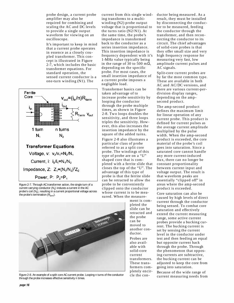
It’s important to keep in mindthat a current probe operatesin essence as a closely cou-pled transformer. This con-cept is illustrated in Figure2-7, which includes the basictransformer equations. Forstandard operation, thesensed current conductor is aone-turn winding (N1). The
Figure 2-7. Through AC transformer action, the single turn of acurrent carrying conductor (N1) induces a current in the ACprobe’s coil (N2), resulting in a current proportional voltage acrossthe probe’s termination (Rterm).
Figure 2-8. An example of a split core AC current probe. Looping n turns of the conductorthrough the probe increases effective sensitivity n times.

page 17
milliamps to kiloamps, fromDC to MHz there’s a corre-spondingly wide selection ofcurrent probes. Choosing acurrent probe for a particularapplication is similar inmany respects to selectingvoltage probes. Current han-dling capability, sensitivityranges, insertion impedance,connectability, and band-width/rise-time limits aresome of the key selection cri-teria. Additionally, currenthandling capability must bederated with frequency andthe probe’s specified amp-second product must not beexceeded.
Logic probes. Faults in digitalsystems can occur for a vari-ety of reasons. While a logicanalyzer is the primary toolfor identifying and isolatingfault occurrences, the actualcause of the logic fault isoften due to the analogattributes of the digital wave-form. Pulse width jitter, pulseamplitude aberrations, andregular old analog noise andcrosstalk are but a few of themany possible analog causesof digital faults.
Analyzing the analogattributes of digital wave-forms requires use of an oscil-loscope. However, to isolateexact causes, digital designersoften need to look at specificdata pulses occurring duringspecific logic conditions.This requires a logic trigger-ing capability that is moretypical of a logic analyzerthan an oscilloscope. Suchlogic triggering can be addedto most oscilloscopes throughuse of a word recognizer trig-ger probe such as shown inFigure 2-9.
The particular probe shownin Figure 2-9 is designed forTTL and TTL-compatiblelogic. It can provide up to 17data-channel probes (16 databits plus qualifier), and iscompatible with both syn-chronous and asynchronousoperation. The trigger word
Figure 2-9. A word recognizer probe. Such probes allow oscilloscopes to be used to analyze specific data wave-forms during specific logic conditions.
NEW TERMaberrations – Any deviation fromthe ideal or norm; usually associ-ated with the flat tops and bases ofwaveforms or pulses. Signals mayhave aberrations caused by the cir-cuit conditions of the signal source,and aberrations may be impressedupon a signal by the measurementsystem. In any measurement whereaberrations are involved, it isimportant to determine whether theaberrations are actually part of thesignal or the result of the measure-ment process. Generally, aberrationsare specified as a percentage devia-tion from a flat response.

page 18
communication system trou-bleshooting and analysis.However, there’s also anexpanding need for general-purpose optical waveformmeasurement and analysisduring optical componentdevelopment and verification.Optical probes fill this needby allowing optical signals tobe viewed on an oscilloscope.
The optical probe is an opti-cal-to-electrical converter. Onthe optical side, the probemust be selected to match thespecific optical connectorand fiber type or opticalmode of the device that’sbeing measured. On the elec-trical side, the standardprobe-to-scope matching cri-teria are followed.
Other probe types. In addi-tion to all of the above “fairlystandard” probe types,there’s also a variety of spe-cialty probes and probingsystems. These include:
•Environmental probes,which are designed to oper-ate over a very wide tem-perature range.
•Temperature probes, whichare used to measure thetemperature of componentsand other heat generatingitems.
•Probing stations and articu-lated arms (Figure 2-10) forprobing fine-pitch devicessuch as multi-chip-mod-ules, hybrid circuits, andICs.
Floating MeasurementsFloating measurements aremeasurements that are madebetween two points, neitherof which is at ground poten-tial. If this sounds a lot likedifferential measurementsdescribed previously withregard to differential probes,you’re right. A floating mea-surement is a differentialmeasurement, and, in fact,floating measurements can bemade using differentialprobes.
Generally, however, the term“floating measurement” isused in referring to powersystem measurements. Exam-ples are switching supplies,motor drives, ballasts, anduninterruptible power sourceswhere neither point of themeasurement is at ground(earth potential), and the sig-nal “common” may be ele-vated (floating) to hundreds ofvolts from ground. Often,these measurements requirerejection of high common-mode signals in order to eval-uate low-level signals ridingon them. Extraneous groundcurrents can also add hum tothe display, causing evenmore measurement difficulty.
An example of a typical float-ing measurement situation isshown in Figure 2-11. In thismotor drive system, the three-phase AC line is rectified to afloating DC bus of up to600 V. The ground-referencedcontrol circuit generatespulse modulated gate drivesignals through an isolateddriver to the bridge transis-tors, causing each output toswing the full bus voltage atthe pulse modulation fre-quency. Accurate measure-ment of the gate-to-emittervoltage requires rejection ofthe bus transitions. Addition-ally, the compact design ofthe motor drive, fast currenttransitions, and proximity tothe rotating motor contributeto a harsh EMI environment.Also, connecting the groundlead of a scope’s probe to anypart of the motor drive circuitwould cause a short toground.
to be recognized is pro-grammed into the probe bymanually setting miniatureswitches on the probe head.When a matching word is rec-ognized, the probe outputs aHi (one) trigger pulse that canbe used to trigger oscillo-scope acquisition of relateddata waveforms or events.
Optical probes. With theadvent and spread of fiber-optic based communications,there’s a rapidly expandingneed for viewing and analyz-ing optical waveforms. A vari-ety of specialized optical sys-tem analyzers have beendeveloped to fill the needs of
Figure 2-11. In this three-phase motor drive, all points are above ground, making floating measurements a necessity.
Figure 2-10. Example of a probing station designed for probingsmall geometry devices such as hybrid circuits and ICs.

page 19
DANGERTo get around this directshort to ground, some scopeusers have used the unsafepractice of defeating theoscilloscope’s ground cir-cuit. This allows the scope’sground lead to float with themotor drive circuit so thatdifferential measurementscan be made. Unfortunately,this practice also allows thescope chassis to float atpotentials that could be adangerous or deadly shockhazard to the scope user.
Not only is “floating” theoscilloscope an unsafe prac-tice, but the resulting mea-surements are oftenimpaired by noise and othereffects. This is illustrated inFigure 2-12a, which shows afloated oscilloscope mea-surement of one of the gate-to-emitter voltages on themotor drive unit. The bot-tom trace in Figure 2-12a isthe low-side gate-emittervoltage and the top trace isthe high-side voltage. Noticethe significant ringing onboth of these traces. Thisringing is due to the largeparasitic capacitance fromthe scope’s chassis to earthground.
Figure 2-12b shows theresults of the same measure-ment, but this time madewith the scope properlygrounded and the measure-ment made through a probeisolator. Not only has theringing been eliminatedfrom the measurement, butthe measurement can bemade in far greater safetybecause the scope is nolonger floating aboveground.
Rather than floating thescope, the probe isolatorfloats just the probe. This iso-lation of the probe can bedone via either a transformeror optical coupling mecha-nism, as shown in Figure2-13. In this case, the scoperemains grounded, as itshould, and the differentialsignal is applied to the tipand reference lead of the iso-lated probe. The isolatortransmits the differential sig-nal through the isolator to areceiver, which produces aground-referenced signal thatis proportional to the differ-ential input signal. Thismakes the probe isolator com-patible with virtually anyinstrument.
To meet different needs, vari-ous types of isolators areavailable. These includemulti-channel isolators thatprovide two or more chan-nels with independent refer-ence leads. Also, fiber-opticbased isolators are availablefor cases where the isolatorneeds to be physically sepa-rated from the instrument bylong distances (e.g. 100meters or more). As with dif-ferential probes, the key iso-lator selection criteria arebandwidth and CMRR. Addi-tionally, maximum workingvoltage is a key specificationfor isolation systems. Typi-cally, this is 600 V RMS or850 V (DC+peak AC).
Figure 2-13. Example of probe isolation for making floating measurements.
Figure 2-12. In addition to being dangerous, floating an oscillo-scope can result in significant ringing on measurements (a) ascompared to the safer method of using a probe isolator (b).
a.
b.

page 20
Probe AccessoriesMost probes come with apackage of standard acces-sories. These accessoriesoften include a ground leadclip that attaches to theprobe, a compensation adjust-ment tool, and one or moreprobe tip accessories to aid inattaching the probe to varioustest points. Figure 2-14 showsan example of a typical gen-eral-purpose voltage probeand its standard accessories.
Probes that are designed forspecific application areas,such as probing surfacemount devices, may includeadditional probe tip adaptersin their standard accessoriespackage. Also, various spe-cial purpose accessories maybe available as options for theprobe. Figure 2-15 illustratesseveral types of probe tipadaptors designed for usewith small geometry probes.
It’s important to realize thatmost probe accessories, espe-cially probe tip adaptors, aredesigned to work with spe-cific probe models. Switch-ing adaptors between probemodels or probe manufactur-ers is not recommended sinceit can result in poor connec-tion to the test point or dam-age to either the probe orprobe adaptor.
When selecting probes forpurchase, it’s also importantto take into account the typeof circuitry that you’ll beprobing and any adaptors oraccessories that will makeprobing quicker and easier.In many cases, less expensivecommodity probes don’t pro-vide a selection of adaptoroptions. On the other hand,probes obtained through anoscilloscope manufactureroften have an extremelybroad selection of accessoriesfor adapting the probe to spe-cial needs. An example ofthis is shown in Figure 2-16,which illustrates the varietyof accessories and optionsavailable for a particularclass of probes. These acces-sories and options will, ofcourse, vary between differ-ent probe classes and models.
Figure 2-15. Some examples of probe tip adaptors for small geometry probes. Such adapters make probing ofsmall circuitry significantly easier and can enhance measurement accuracy by providing high integrity probe totest point connections.
Figure 2-14. A typical general-purpose voltage probe with its standard accessories.
AdjustmentTool
Clip-On GroundLead
Retractable HookTip Adapter

page 21
Figure 2-16. An example of the various accessories that are available for a 5-mm (miniature) probe system. Other probe families will have differing accessoriesdepending on the intended application for that family of probes.

page 22

page 23
The Effect of Source ImpedanceThe value of the sourceimpedance can significantlyinfluence the net effect of anyprobe loading. For example,with low source impedances,the loading effect of a typicalhigh-impedance 10X probewould be hardly noticeable.This is because a highimpedance added in parallelwith a low impedance pro-duces no significant changein total impedance.
However, the story changesdramatically with highersource impedances. Consider,for example, the case wherethe source impedances in Fig-ure 3-1 have the same value,and that value equals thetotal of the probe and scopeimpedances. This situation isillustrated in Figure 3-2.
For equal values of Z, thesource load is 2Z without theprobe and scope attached tothe test point (see Figure3-2a). This results in a signalamplitude of 0.5ES at theunprobed test point. How-ever, when the probe and
scope are attached (Figure3-2b), the total load on thesource becomes 1.5Z, and thesignal amplitude at the testpoint is reduced to two-thirdsof its unprobed value.
In this latter case, there aretwo approaches that can betaken to reduce theimpedance loading effects ofprobing. One approach is touse a higher impedanceprobe. The other is to probethe signal somewhere else inthe circuit at a test point thathas a lower impedance. Forexample, cathodes, emitters,and sources usually havelower impedances thanplates, collectors, or drains.
Capacitive LoadingAs signal frequencies or tran-sition speeds increase, thecapacitive element of theimpedances becomes pre-dominate. Consequently,capacitive loading becomes amatter of increasing concern.In particular, capacitive load-ing will affect the rise and falltimes on fast-transition wave-forms and the amplitudes of
To obtain an oscilloscope dis-play of a signal, some portionof the signal must be divertedto the scope’s input circuit.This is illustrated in Figure3-1, where the circuitrybehind the test point, TP, isrepresented by a signalsource, ES, and the associatedcircuit impedances, ZS1 andZS2, that are the normal loadon ES. When an oscilloscopeis attached to the test point,the probe impedance, Zp, andscope input impedance, Zi,become part of the load onthe signal source.
Depending on the relativevalues of the impedances,addition of the probe andscope to the test point causesvarious loading effects. Thischapter explores loadingeffects, as well as other prob-ing effects, in detail.
Figure 3-1. The signal being measured at the test point (TP) can be repre-sented by a signal source and associated load impedances (a). Probing thetest point adds the probe and scope impedances to the source load, resultingin some current draw by the measurement system (b).
Figure 3-2.The higher the source impedances, the greater the loading causedby probing. In this case, the impedances are all equal and probing causes amore than 30% reduction in signal amplitude at the test point.
Chapter 3: How Probes Affect Your Measurements
NEW TERMsource impedance – The impedanceseen when looking back into asource.

page 24
this zero rise time is modifiedthrough integration by theassociated resistance andcapacitance of the sourceimpedance load.
The RC integration networkalways produces a 10 to 90%rise time of 2.2RC. This isderived from the universaltime-constant curve of acapacitor. The value of 2.2 isthe number of RC time con-stants necessary for C tocharge through R from the10% value to the 90% ampli-tude value of the pulse.
In the case of Figure 3-3, the50 Ω and 20 pF of the sourceimpedance results in a pulserise time of 2.2 ns. This 2.2RCvalue is the fastest rise timethat the pulse can have.
When the pulse generator’soutput is probed, the probe’sinput capacitance and resis-tance are added to that of thepulse generator. This isshown in Figure 3-4, wherethe 10 MΩ and 11 pF of a typ-ical probe have been added.Since the probe’s 10 MΩresistance is so much greaterthan the generator’s 50 Ωresistance, the probe’s resis-tance can be ignored. How-ever, the probe’s capacitanceis in parallel with the loadcapacitance and adds to itdirectly for a total loadcapacitance of 31 pF. Thisincreases the value of 2.2RCand results in an increase inthe measured rise time to3.4 ns versus the 2.2 ns previ-ous to probing.
You can estimate the effect ofprobe tip capacitance on risetime by taking the ratio of theprobe’s specified capacitanceto the known or estimatedsource capacitance. Using thevalues from Figure 3-4 thiswould result in the followingestimate of percentagechange in rise time:
Cprobe tipx 100%
C1
= 11 pF
x 100%20 pF
= 55%
From the above, it’s clear thatprobe choice, especially withregard to probe capacitance,can affect your rise-time mea-surements. For passiveprobes, the greater the attenu-ation ratio, the lower the tipcapacitance in general. Thisis indicated in Table 3-1which lists some probecapacitance examples for var-ious passive probes.
Where smaller tip capaci-tance is needed, active FET-input probes should be used.Depending on the specific
high-frequency componentsin waveforms.
Effect on rise time. To illus-trate capacitive loading, let’sconsider a pulse generatorwith a very fast rise time.This is shown in Figure 3-3,where the pulse at the idealgenerator’s output has a risetime of zero (tr = 0). However,
Figure 3-3. The rise time of a pulse generator is determined by its RC load.
Figure 3-4. The added capacitance of a probe increases RC the value and increases the measured rise time.
Table 3-1. Probe Tip CapacitanceProbe Attenuation Tip Capacitance
Tektronix P6101B 1X 54 pF
Tektronix P6105A 10X 11.2 pF
Tektronix P5100 100X 2.75 pF

page 25
curves showing Zp versus fre-quency. Figure 3-5 is anexample of such a curve forthe Tektronix P6205 ActiveProbe. Notice that the 1 MΩimpedance magnitude is con-stant to nearly 100 kHz. Thiswas done by careful design ofthe probe’s associated resis-tive, capacitive, and induc-tive elements.
Figure 3-6 shows anotherexample of a probe curve. Inthis case Rp and Xp versus fre-quency are shown for a typi-cal 10 MΩ passive probe. Thedotted line (Xp) shows capac-itive reactance versus fre-quency. Notice that Xp beginsdecreasing at DC, but Rpdoesn’t start rolling off signif-icantly until 100 kHz. Again,the total loading has been off-set by careful design of theassociated R, C, and L ele-ments.
If you don’t have access to aprobe’s impedance curves,you can make a worst-caseloading estimate using thefollowing formula:
Xp = 1
2 π f C
where:
Xp = capacitive reactancef = frequencyC = probe tip capacitance
For example, a standard pas-sive 10 MΩ probe with a tipcapacitance of 11 pF has acapacitive reactance (Xp) ofabout 290 Ω at 50 MHz.Depending on the signalsource impedance, this load-ing could have a major effecton the signal amplitude (bysimple divider action), and itcould even affect the opera-tion of the circuit beingprobed.
Bandwidth ConsiderationsBandwidth is a measurementsystem issue that involvesboth the bandwidth of theprobe and the oscilloscope.The oscilloscope’s bandwidthshould exceed the predomi-nate frequencies of the signalsyou want to measure, and thebandwidth of the probe usedshould equal or exceed thebandwidth of the scope.
From a measurement systemperspective, the real concernis the bandwidth at the probetip. Often, manufacturers willspecify bandwidth at theprobe tip for certain oscillo-scope/probe combinations.This is not always the case,though. Consequently, youshould be aware of the majorbandwidth issues of an oscil-loscope and a probe, bothindividually and in combina-tion.
active probe model, tipcapacitances of 1 pF and lessare available.
Effect on amplitude andphase. In addition to affectingrise time, capacitive loadingalso affects the amplitude andphase of the high-frequencycomponents in a waveform.With regard to this, it isimportant to keep in mindthat all waveforms are com-posed of sinusoidal compo-nents. A 50 MHz square wavewill have harmonic compo-nents of significance beyond100 MHz. Thus, it’s impor-tant to not only considerloading effects at a wave-form’s fundamental fre-quency but also at frequen-cies several multiples abovethe fundamental.
Loading is determined by thetotal impedance at the probetip. This is designated as Zp,and Zp is composed of a resis-tive component, Rp, and reac-tive component Xp. The reac-tive component is predomi-nantly capacitive, althoughinductive elements may bedesigned into the probe topartially offset capacitiveloading.
As a rule, Zp decreases withincreasing frequency. Mostprobe instruction manualsdocument probe Rp with
Figure 3-5. Typical input impedance versus frequency for the TektronixP6205 Active Probe.
Figure 3-6. Xp and Rp versus frequency for a typical 10 MΩ passive probe.
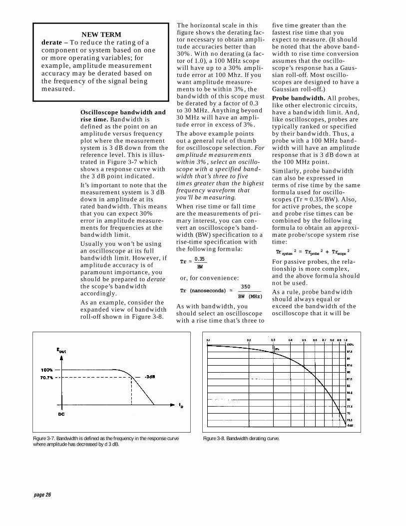
page 26
The horizontal scale in thisfigure shows the derating fac-tor necessary to obtain ampli-tude accuracies better than30%. With no derating (a fac-tor of 1.0), a 100 MHz scopewill have up to a 30% ampli-tude error at 100 Mhz. If youwant amplitude measure-ments to be within 3%, thebandwidth of this scope mustbe derated by a factor of 0.3to 30 MHz. Anything beyond30 MHz will have an ampli-tude error in excess of 3%.
The above example pointsout a general rule of thumbfor oscilloscope selection. Foramplitude measurementswithin 3%, select an oscillo-scope with a specified band-width that’s three to fivetimes greater than the highestfrequency waveform thatyou’ll be measuring.
When rise time or fall timeare the measurements of pri-mary interest, you can con-vert an oscilloscope’s band-width (BW) specification to arise-time specification withthe following formula:
Tr ≈ 0 . 3 5B W
or, for convenience:
Tr (nanoseconds) ≈ 350
BW (MHz)
As with bandwidth, youshould select an oscilloscopewith a rise time that’s three to
five time greater than thefastest rise time that youexpect to measure. (It shouldbe noted that the above band-width to rise time conversionassumes that the oscillo-scope’s response has a Gaus-sian roll-off. Most oscillo-scopes are designed to have aGaussian roll-off.)
Probe bandwidth. All probes,like other electronic circuits,have a bandwidth limit. And,like oscilloscopes, probes aretypically ranked or specifiedby their bandwidth. Thus, aprobe with a 100 MHz band-width will have an amplituderesponse that is 3 dB down atthe 100 MHz point.
Similarly, probe bandwidthcan also be expressed interms of rise time by the sameformula used for oscillo-scopes (Tr ≈ 0.35/BW). Also,for active probes, the scopeand probe rise times can becombined by the followingformula to obtain an approxi-mate probe/scope system risetime:
T rs y s t e m2 ≈ Trp r o b e 2 + Trs c o p e 2
For passive probes, the rela-tionship is more complex,and the above formula shouldnot be used.
As a rule, probe bandwidthshould always equal orexceed the bandwidth of theoscilloscope that it will be
Oscilloscope bandwidth andrise time. Bandwidth isdefined as the point on anamplitude versus frequencyplot where the measurementsystem is 3 dB down from thereference level. This is illus-trated in Figure 3-7 whichshows a response curve withthe 3 dB point indicated.
It’s important to note that themeasurement system is 3 dBdown in amplitude at itsrated bandwidth. This meansthat you can expect 30%error in amplitude measure-ments for frequencies at thebandwidth limit.
Usually you won’t be usingan oscilloscope at its fullbandwidth limit. However, ifamplitude accuracy is ofparamount importance, youshould be prepared to deratethe scope’s bandwidthaccordingly.
As an example, consider theexpanded view of bandwidthroll-off shown in Figure 3-8.
Figure 3-7. Bandwidth is defined as the frequency in the response curvewhere amplitude has decreased by d 3 dB.
Figure 3-8. Bandwidth derating curve.
NEW TERMderate – To reduce the rating of acomponent or system based on oneor more operating variables; forexample, amplitude measurementaccuracy may be derated based onthe frequency of the signal beingmeasured.
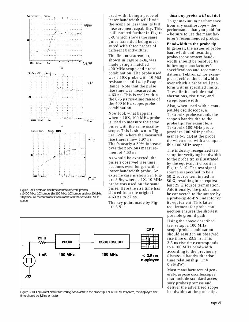
page 27
used with. Using a probe oflesser bandwidth will limitthe scope to less than its fullmeasurement capability. Thisis illustrated further in Figure3-9, which shows the samepulse transition being mea-sured with three probes ofdifferent bandwidths.
The first measurement,shown in Figure 3-9a, wasmade using a matched400 MHz scope and probecombination. The probe usedwas a 10X probe with 10 MΩresistance and 14.1 pF capac-itance. Note that the pulserise time was measured as4.63 ns. This is well withinthe 875 ps rise-time range ofthe 400 MHz scope/probecombination.
Now look what happenswhen a 10X, 100 MHz probeis used to measure the samepulse with the same oscillo-scope. This is shown in Fig-ure 3-9b, where the measuredrise time is now 5.97 ns.That’s nearly a 30% increaseover the previous measure-ment of 4.63 ns!
As would be expected, thepulse’s observed rise timebecomes even longer with alower bandwidth probe. Anextreme case is shown in Fig-ure 3-9c, where a 1X, 10 MHzprobe was used on the samepulse. Here the rise time hasslowed from the original4.63 ns to 27 ns.
The key point made by Fig-ure 3-9 is:
Just any probe will not do!
To get maximum performancefrom any oscilloscope – theperformance that you paid for– be sure to use the manufac-turer’s recommended probes.
Bandwidth to the probe tip.In general, the issues of probebandwidth and resultingprobe/scope system band-width should be resolved byfollowing manufacturer’sspecifications and recommen-dations. Tektronix, for exam-ple, specifies the bandwidthover which a probe will per-form within specified limits.These limits include totalaberrations, rise time, andswept bandwidth.
Also, when used with a com-patible oscilloscope, aTektronix probe extends thescope’s bandwidth to theprobe tip. For example, aTektronix 100 MHz probeprovides 100 MHz perfor-mance (–3 dB) at the probetip when used with a compat-ible 100 MHz scope.
The industry recognized testsetup for verifying bandwidthto the probe tip is illustratedby the equivalent circuit inFigure 3-10. The test signalsource is specified to be a50 Ω source terminated in50 Ω, resulting in an equiva-lent 25 Ω source termination.Additionally, the probe mustbe connected to the source bya probe-tip-to-BNC adaptor orits equivalent. This latterrequirement for probe con-nection ensures the shortestpossible ground path.
Using the above describedtest setup, a 100 MHzscope/probe combinationshould result in an observedrise time of ≤3.5 ns. This3.5 ns rise time correspondsto a 100 MHz bandwidthaccording to the previouslydiscussed bandwidth/rise-time relationship (Tr ≈0.35/BW).
Most manufacturers of gen-eral-purpose oscilloscopesthat include standard acces-sory probes promise anddeliver the advertised scopebandwidth at the probe tip.
Figure 3-9. Effects on rise time of three different probes:( a )4 0 0 MHz, 10X probe, (b) 100 MHz, 10X probe, and (c) 10 MHz,1X probe. All measurements were made with the same 400 MHzs c o p e .
Figure 3-10. Equivalent circuit for testing bandwidth to the probe tip. For a 100 MHz system, the displayed risetime should be 3.5 ns or faster.
a.
b.
c.
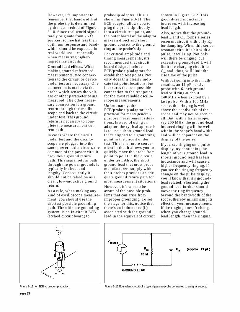
page 28
probe-tip adapter. This isshown in Figure 3-11. TheECB adaptor allows you toplug the probe tip directlyinto a circuit test point, andthe outer barrel of the adaptormakes a direct and shortground contact to the groundring at the probe’s tip.
For critical amplitude andtiming measurements, it’srecommended that circuitboard designs includeECB/probe-tip adaptors forestablished test points. Notonly does this clearly indi-cate test point locations, butit ensures the best possibleconnection to the test pointfor the most reliable oscillo-scope measurements.
Unfortunately, theECB/probe-tip adaptor isn’tpractical for many general-purpose measurement situa-tions. Instead of using anadaptor, the typical approachis to use a short ground leadthat’s clipped to a groundingpoint in the circuit undertest. This is far more conve-nient in that it allows you toquickly move the probe frompoint to point in the circuitunder test. Also, the shortground lead that most probemanufacturers supply withtheir probes provides an ade-quate ground return path formost measurement situations.
However, it’s wise to beaware of the possible prob-lems that can arise fromimproper grounding. To setthe stage for this, notice thatthere’s an inductance (L)associated with the groundlead in the equivalent circuit
shown in Figure 3-12. Thisground-lead inductanceincreases with increasinglead length.
Also, notice that the ground-lead L and Cin forms a seriesresonant circuit with only Rinfor damping. When this seriesresonant circuit is hit with apulse, it will ring. Not onlywill there be ringing, butexcessive ground-lead L willlimit the charging circuit toCin and, thus, will limit therise time of the pulse.
Without going into the math-ematics, an 11 pF passiveprobe with 6-inch groundlead will ring at about140 MHz when excited by afast pulse. With a 100 MHzscope, this ringing is wellabove the bandwidth of thescope and may not be seen atall. But, with a faster scope,say 200 MHz, the ground-leadinduced ringing will be wellwithin the scope’s bandwidthand will be apparent on thedisplay of the pulse.
If you see ringing on a pulsedisplay, try shortening thelength of your ground lead. Ashorter ground lead has lessinductance and will cause ahigher frequency ringing. Ifyou see the ringing frequencychange on the pulse display,you’ll know that it’s ground-lead related. Shortening theground lead further shouldmove the ring frequencybeyond the bandwidth of thescope, thereby minimizing itseffect on your measurements.If the ringing doesn’t changewhen you change ground-lead length, then the ringing
However, it’s important toremember that bandwidth atthe probe tip is determinedby the test method of Figure3-10. Since real-world signalsrarely originate from 25 Ωsources, somewhat less thanoptimum response and band-width should be expected inreal-world use – especiallywhen measuring higher-impedance circuits.
Ground lead effects. Whenmaking ground-referencedmeasurements, two connec-tions to the circuit or deviceunder test are necessary. Oneconnection is made via theprobe which senses the volt-age or other parameter beingmeasured. The other neces-sary connection is a groundreturn through the oscillo-scope and back to the circuitunder test. This groundreturn is necessary to com-plete the measurement cur-rent path.
In cases where the circuitunder test and the oscillo-scope are plugged into thesame power outlet circuit, thecommon of the power circuitprovides a ground returnpath. This signal return paththrough the power grounds istypically indirect andlengthy. Consequently itshould not be relied on as aclean, low-inductive groundreturn.
As a rule, when making anykind of oscilloscope measure-ment, you should use theshortest possible groundingpath. The ultimate groundingsystem, is an in-circuit ECB(etched circuit board) to
Figure 3-11. An ECB to probe-tip adaptor. Figure 3-12 Equivalent circuit of a typical passive probe connected to a signal source.

•Select the probes that bestmatch your application’sneeds in terms of both mea-surement capabilities andmechanical attachment totest points.
And finally, always be awareof the possible probe loadingeffects on the circuit beingprobed. In many cases, load-ing can be controlled or min-imized through probe selec-tion. The following summa-rizes some of the probe load-ing considerations to beaware of:
Passive probes. 1X passiveprobes typically have a lowerresistance and higher capaci-tance than 10X passiveprobes. As a result, 1X probesare more prone to cause load-ing, and whenever possible10X probes should be usedfor general-purpose probing.
Voltage divider (Zo) probes.These probes have very lowtip capacitance, but at theexpense of relatively highresistive loading. They’reintended for use whereimpedance matching isrequired in 50 Ω environ-ments. However, because oftheir very high bandwidth/-rise-time capabilities, voltagedivider probes are often usedin other environments forhigh-speed timing measure-ments. For amplitude mea-surements, the effect of theprobe’s low input R shouldbe taken into account.
Bias-offset probes. A bias-off-set probe is a special type ofvoltage divider probe withthe capability of providing avariable offset voltage at theprobe tip. These probes areuseful for probing high-speedECL circuitry, where resistiveloading could upset the cir-cuit’s operating point.
Active probes. Active probescan provide the best of bothworlds with very low resis-tive loading and very low tipcapacitance. The trade-off isthat active probes typicallyhave a low dynamic range.However, if your measure-ments fit within the range ofan active probe, this can bethe best choice in manycases.
page 29
move the ground clip eachtime different points areprobed in a large system.Unfortunately, this practicelengthens the ground loopand can cause severe ringing,as shown in Figure 3-13b.
Figure 3-13c, shows theresults of another variation oflengthening the ground loop.In this case, the probe’sground lead wasn’t connectedat all. Instead, a separate, 28-inch clip lead was run fromthe circuit common to thescope chassis. This created adifferent, and apparentlylonger, ground loop, resultingin the lower frequency ring-ing seen in Figure 3-13c.
From the examples in Figure3-13, it’s clear that groundingpractices have tremendousimpact on measurement qual-ity. Specifically, probe groundleads need to be kept as shortand direct as possible.
What to do About Probing EffectsFrom the preceding examplesand discussion, we’ve seenthat the signal sourceimpedance, the probe, andthe oscilloscope form aninteractive system. For opti-mum measurement results,you need to do everythingpossible to minimize thescope/probe affects on thesignal source. The followinggeneral rules will help you indoing this:
•Always match your scopeand probes according to thescope manufacturer’s rec-ommendations.
•Make sure that yourscope/probe has adequatebandwidth or rise-timecapabilities for the signalyou’re trying to measure.Typically, you shouldselect a scope/probe combi-nation with a rise timespecification that’s three tofive times faster than thefastest rise time you plan tomeasure.
•Always keep your probeground leads as short anddirect as possible. Exces-sive ground loops cancause ringing on pulses.
is likely being induced in thecircuit under test.
Figure 3-13 illustrates groundlead induced ringing further.In Figure 3-13a, a matchedscope/probe combination wasused to acquire a fast transi-tion. The ground lead usedwas the standard 6.5-inchprobe ground clip, and it wasattached to a common nearthe test point.
In Figure 3-13b, the samepulse transition is acquired.This time, however, theprobe’s standard ground leadwas extended with a 28-inchclip lead. This ground leadextension might be done, forexample, to avoid having to
Figure 3-13. Ground lead length and placement can dramaticallyaffect measurements.
a.
b.
c.

page 30

page 31
Most of the key probe specifi-cations have been discussedin preceding chapters, eitherin terms of probe types or interms of how probes affectmeasurements. This chaptergathers all of those key probespecification parameters andterms into one place for eas-ier reference.
The following list of specifi-cations is presented in alpha-betical order; not all of thesespecifications will apply toany given probe. For exam-ple, Insertion Impedance is aspecification that applies tocurrent probes only. Otherspecifications, such as Band-width, are universal andapply to all probes.
Aberrations (universal)An aberration is any ampli-tude deviation from theexpected or ideal response toan input signal. In practice,aberrations usually occurimmediately after fast wave-form transitions and appearas what’s sometimes referredto as “ringing.”
Aberrations are measured, orspecified, as a ± percentagedeviation from the final pulseresponse level (see Figure4-1). This specification mightalso include a time windowfor the aberrations. An exam-ple of this would be:
Aberrations should notexceed ±3% or 5% peak-to-peak within the first 30nanoseconds...
When excessive aberrationsare seen on a pulse measure-ment, be sure to consider allpossible sources beforeassuming that the aberrationsare the fault of the probe. Forexample, are the aberrationsactually part of the signalsource? Or are they the resultof the probe grounding tech-nique?
One of the most commonsources of observed aberra-tions is neglecting to checkand properly adjust the com-pensation of voltage probes.A severely over-compensatedprobe will result in signifi-cant peaks immediately fol-lowing pulse edges (see Fig-ure 4-2).
Amp-Second Product (currentprobes)For current probes, amp-sec-ond product specifies theenergy handling capability ofthe current transformer’score. If the product of theaverage current and pulsewidth exceeds the amp-sec-ond rating, the core saturates.This core saturation results ina clipping off or suppressionof those portions of the wave-form occurring during satura-tion. If the amp-second prod-uct is not exceeded, the sig-nal voltage output of theprobe will be linear and themeasurement accurate.
Attenuation Factor (universal)All probes have an attenua-tion factor, and some probesmay have selectable attenua-tion factors. Typical attenua-tion factors are 1X, 10X, and100X.
The attenuation factor is theamount by which the probereduces signal amplitude. A1X probe doesn’t reduce, orattenuate, the signal, while a10X probe reduces the signalto 1/10th of its probe tipamplitude. Probe attenuationfactors allow the measure-ment range of an oscilloscopeto be extended. For example,a 100X probe allows signalsof 100 times greater ampli-tude to be measured.
The 1X, 10X, 100X designa-tions stem from the dayswhen oscilloscopes didn’tautomatically sense probeattenuation and adjust scalefactor accordingly. The 10Xdesignation, for example,reminded you that all ampli-tude measurements needed tobe multiplied by 10. Thereadout systems on today’soscilloscopes automaticallysense probe attenuation fac-tors and adjust the scale fac-tor readouts accordingly.
Voltage probe attenuation fac-tors are achieved using resis-tive voltage divider tech-niques. Consequently, probeswith higher attenuation fac-tors typically have higherinput resistances. Also the
Chapter 4: Understanding Probe Specifications
Figure 4-1. An example of measuring aberrations relative to 100% pulse height. Figure 4-2. Aberrations from over compensating a probe.

page 32
amplitude to fall to 70.7%(–3 dB), as indicated in Fig-ure 4-3.
It should also be noted thatsome probes have a low-fre-quency bandwidth limit aswell. This is the case, forexample, with AC currentprobes. Because of theirdesign, AC current probescannot pass DC or low-fre-quency signals. Thus, theirbandwidth must be specifiedwith two values, one for lowfrequency and one for highfrequency.
For oscilloscope measure-ments, the real concern is theoverall bandwidth of thescope and probe combined.This system performance iswhat ultimately determinesmeasurement capability.Unfortunately, attaching aprobe to an oscilloscoperesults in some degradationof bandwidth performance.For example, using a100 MHz generic probe witha 100 MHz oscilloscoperesults in a measurement sys-tem with a bandwidth perfor-mance that is something lessthan 100 MHz. To avoid theuncertainty of overall systembandwidth performance,Tektronix specifies its pas-sive voltage probes to providea specified measurement sys-tem bandwidth at the probetip when used with the desig-nated scope models.
In selecting oscilloscopes andoscilloscope probes, it’simportant to realize thatbandwidth has several impli-cations for measurementaccuracy.
In terms of amplitude mea-surements, a sine wave’samplitude becomes increas-ingly attenuated as the sinewave frequency approachesthe bandwidth limit. At thebandwidth limit, the sinewave’s amplitude will bemeasured as being 70.7% ofits actual amplitude. Thus,for greater amplitude mea-surement accuracy, it’s nec-essary to select oscilloscopesand probes with bandwidthsseveral times greater than the
highest frequency waveformthat you plan to measure.
The same holds true for mea-suring waveform rise and falltimes. Waveform transitions,such as pulse and squarewave edges, are made up ofhigh-frequency components.Attenuation of these high-fre-quency components by abandwidth limit results in thetransition appearing slowerthan it really is. For accuraterise-and fall-time measure-ments, it’s necessary to use ameasurement system withadequate bandwidth to pre-serve the high frequenciesthat make up the waveform’srise and fall times. This ismost often stated in terms ofa measurement system risetime, which should typicallybe four to five times fasterthan the rise times that youare trying to measure.
Capacitance (universal)Generally, probe capacitancespecifications refer to thecapacitance at the probe tip.This is the capacitance thatthe probe adds to the circuittest point or device undertest.
Probe tip capacitance isimportant because it affectshow pulses are measured. Alow tip capacitance mini-mizes errors in making rise-time measurements. Also, if apulse’s duration is less thanfive times the probe’s RC timeconstant, the amplitude of thepulse is affected.
Probes also present a capaci-tance to the input of the oscil-loscope, and this probecapacitance should matchthat of the oscilloscope. For10X and 100X probes, thiscapacitance is referred to as acompensation range, which isdifferent than tip capacitance.For probe matching, the oscil-loscope’s input capacitanceshould be within the com-pensation range of the probe.
CMRR (differential probes)Common-mode rejection ratio(CMRR) is a differentialprobe’s ability to reject anysignal that is common to bothtest points in a differential
divider effect splits probecapacitance, effectively pre-senting lower probe tipcapacitance for higher attenu-ation factors.
Accuracy (universal)For voltage-sensing probes,accuracy generally refers tothe probe’s attenuation of aDC signal. The calculationsand measurements of probeaccuracy generally shouldinclude the oscilloscope’sinput resistance. Thus, aprobe’s accuracy specifica-tion is only correct or appli-cable when the probe is beingused with an oscilloscopehaving the assumed inputresistance. An example accu-racy specification would be:
10X within 3% (for scopeinput of 1 MΩ ±2%).
For current-sensing probes,the accuracy specificationrefers to the accuracy of thecurrent-to-voltage conversion.This depends on the currenttransformer turns ratio andthe value and accuracy of theterminating resistance. Cur-rent probes that work withdedicated amplifiers haveoutputs that are calibrateddirectly in amps/div andhave accuracy specificationsthat are given in terms ofattenuator accuracy as a per-centage of the current/divi-sion setting.
Bandwidth (universal)All probes have bandwidth.A 10 MHz probe has a10 MHz bandwidth, and a100 MHz probe has a100 MHz bandwidth. Thebandwidth of a probe is thatfrequency where the probe’sresponse causes output
Figure 4-3.Bandwidth is that frequency in the response curvewhere a sine wave’s amplitude is decreased by 70.7% (–3 dB).
page 33
With larger L/R ratios, longercurrent pulses can be repre-sented without significantdecay or droop in amplitude.With smaller L/R ratios, long-duration pulses will be seenas decaying to zero before thepulse is actually completed.
Direct Current (current probes)Direct current decreases thepermeability of a currentprobe’s coil core. Thisdecreased permeabilityresults in a decreased coilinductance and L/R time con-stant. The result is reducedcoupling performance for lowfrequencies and loss of mea-surement response for low-frequency currents. Some ACcurrent probes offer current-bucking options that null theeffects of DC.
Insertion Impedance (currentprobes)Insertion impedance is theimpedance that is trans-formed from the currentprobe’s coil (the secondary)into the current carrying con-ductor (the primary) that’sbeing measured. Typically, acurrent probe’s reflectedimpedance values are in therange of milliOhms and pre-sent an insignificant effect oncircuits of 25 Ω or moreimpedance.
Input Capacitance (universal)The probe capacitance mea-sured at the probe tip.
Input Resistance (universal)A probe’s input resistance isthe impedance that the probeplaces on the test point atzero Hertz (DC).
Maximum Input Current Rating(current probes)The maximum input currentrating is the total current (DCplus peak AC) that the probewill accept and still performas specified. In AC currentmeasurements, peak-to-peakvalues must be derated versusfrequency to calculate themaximum total input current.
Maximum Peak Pulse CurrentRating (current probes)This rating should not beexceeded. It takes into
account core saturation anddevelopment of potentiallydamaging secondary voltages.The maximum peak pulsecurrent rating is usuallystated as an amp-secondproduct.
Maximum Voltage Rating(universal)Voltages approaching aprobe’s maximum ratingshould be avoided. The maxi-mum voltage rating is deter-mined by the breakdownvoltage rating of the probebody or the probe compo-nents at the measuring point.
Propagation Delay (universal)Every probe offers some smallamount of time delay orphase shift that varies withsignal frequency. This is afunction of the probe compo-nents and the time it takes forthe signal to travel throughthese components from probetip to oscilloscope connector.
Usually, the most significantshift is caused by the probecable. For example, a 42-inchsection of special probe cablehas a 5 ns signal delay. For a1 MHz signal, the 5 ns delayresults in a two-degree phaseshift. A longer cable results incorrespondingly longer signaldelays.
Propagation delay is usuallyonly a concern when compar-ative measurements are beingmade between two or morewaveforms. For example,when measuring time differ-ences between two wave-forms, the waveforms shouldbe acquired using matchedprobes so that each signalexperiences the same propa-gation delay through theprobes.
Another example would bemaking power measurementsby using a voltage probe anda current probe in combina-tion. Since voltage and cur-rent probes are of markedlydifferent construction, theywill have different propaga-tion delays. Whether or notthese delays will have aneffect on the power measure-ment depends on the frequen-cies of the waveforms being
measurement. CMRR is a keyfigure of merit for differentialprobes and amplifiers, and itis defined by:
CMRR = |Ad/ Ac|
where:
Ad = the voltage gain for the difference signal.
Ac = the voltage gain for common-mode signal.
Ideally, Ad should be large,while Ac should equalize tozero, resulting in an infiniteCMRR. In practice, a CMRRof 10,000:1 is consideredquite good. What this meansis that a common-mode inputsignal of 5 volts will berejected to the point where itappears as 0.5 millivolts atthe output. Such rejection isimportant for measuring dif-ference signals in the pres-ence of noise.
Since CMRR decreases withincreasing frequency, the fre-quency at which CMRR isspecified is as important asthe CMRR value. A differen-tial probe with a high CMRRat a high frequency is betterthan a differential probe withthe same CMRR at a lowerfrequency.
CW Frequency Current Derating(current probes)Current probe specificationsshould include amplitudeversus frequency deratingcurves that relate core satura-tion to increasing frequency.The effect of core saturationwith increasing frequency isthat a waveform with an aver-age current of zero amps willexperience clipping of ampli-tude peaks as the waveform’sfrequency or amplitude isincreased.
Decay Time Constant (currentprobes)The decay time constantspecification indicates a cur-rent probe’s pulse supportingcapability. This time constantis the secondary inductance(probe coil) divided by theterminating resistance. Thedecay time constant is some-times called the probe L/Rratio.

page 34
(scope and probe combined)should be three to five timesfaster than the fastest transi-tion to be measured.
Tangential Noise (active probes)Tangential noise is a methodof specifying probe-generatednoise in active probes. Tan-gential noise figures areapproximately two times theRMS noise.
Temperature Range (universal)Current probes have a maxi-mum operating temperature
that’s the result of heatingeffects from energy inducedinto the coil’s magneticshielding. Increasing temper-ature corresponds toincreased losses. Because ofthis, current probes have amaximum amplitude versusfrequency derating curve.
Attenuator voltage probes(i.e., 10X, 100X, etc.) maybe subject to accuracychanges due to changes int e m p e r a t u r e .
measured. For Hz and kHzsignals, the delay differenceswill generally be insignifi-cant. However, for MHz sig-nals the delay differencesmay have a noticeable effect.
Rise Time (universal)A probe’s 10 to 90% responseto a step function indicatesthe fastest transition that theprobe can transmit from tip toscope input. For accuraterise- and fall-time measure-ments on pulses, the mea-surement system’s rise time

page 35
content, the sourceimpedance, and the physicalattributes of the test point.Each of these issues is cov-ered in the following discus-sion.
Signal type. The first step inprobe selection is to assessthe type of signal to beprobed. For this purpose, sig-nals can be categorized asbeing:
• Voltage Signals• Current Signals• Logic Signals• Other Signals
Voltage signals are the mostcommonly encountered sig-nal type in electronic mea-surements. That accounts forthe voltage-sensing probe asbeing the most common typeof oscilloscope probe. Also, itshould be noted that, sinceoscilloscopes require a volt-age signal at their input, othertypes of oscilloscope probesare, in essence, transducersthat convert the sensed phe-nomenon to a correspondingvoltage signal. A commonexample of this is the currentprobe, which transforms acurrent signal into a voltagesignal for viewing on anoscilloscope.
Logic signals are actually aspecial category of voltagesignals. While a logic signalcan be viewed with a stan-dard voltage probe, it’s moreoften the case that a specificlogic event needs to beviewed. This can be done bysetting a logic probe to pro-vide a trigger signal to theoscilloscope when a specifiedlogic combination occurs.This allows specific logicevents to be viewed on theoscilloscope display.
In addition to voltage, cur-rent, and logic signals, thereare numerous other types ofsignals that may be of inter-est. These can include signalsfrom optical, mechanical,thermal, acoustic, and othersources. Various transducerscan be used to convert suchsignals to corresponding volt-age signals for oscilloscopedisplay and measurement.When this is done, the trans-ducer becomes the signalsource for the purposes ofselecting a probe to conveythe transducer signal to theoscilloscope.
Figure 5-1 provides a graphi-cal categorization of probesbased on the type of signal tobe measured. Notice that
The preceding chapters havecovered a wide range of top-ics regarding oscilloscopeprobes in terms of howprobes function, the varioustypes of probes, and theireffects on measurements. Forthe most part, the focus hasbeen on what happens whenyou connect a probe to a testpoint.
In this chapter, the focuschanges to the signal sourceand how to translate its prop-erties into criteria for appro-priate probe selection. Thegoal, as always, is to selectthe probe that delivers thebest representation of the sig-nal to the oscilloscope. How-ever, it doesn’t stop there.The oscilloscope imposes cer-tain requirements that mustalso be considered as part ofthe probe selection process.This chapter explores the var-ious selection requirements,beginning with understand-ing the requirements imposedby the signal source.
Understanding the Signal SourceThere are four fundamentalsignal source issues to beconsidered in selecting aprobe. These are the signaltype, the signal frequency
Chapter 5: A Guide to Probe Selection
Figure 5-1. Various probe categories based on the signal type to be measured
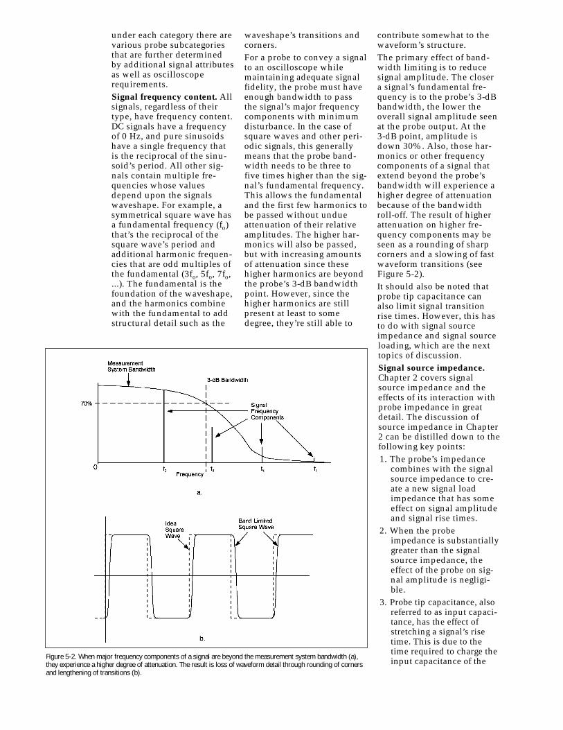
waveshape’s transitions andcorners.
For a probe to convey a signalto an oscilloscope whilemaintaining adequate signalfidelity, the probe must haveenough bandwidth to passthe signal’s major frequencycomponents with minimumdisturbance. In the case ofsquare waves and other peri-odic signals, this generallymeans that the probe band-width needs to be three tofive times higher than the sig-nal’s fundamental frequency.This allows the fundamentaland the first few harmonics tobe passed without undueattenuation of their relativeamplitudes. The higher har-monics will also be passed,but with increasing amountsof attenuation since thesehigher harmonics are beyondthe probe’s 3-dB bandwidthpoint. However, since thehigher harmonics are stillpresent at least to somedegree, they’re still able to
contribute somewhat to thewaveform’s structure.
The primary effect of band-width limiting is to reducesignal amplitude. The closera signal’s fundamental fre-quency is to the probe’s 3-dBbandwidth, the lower theoverall signal amplitude seenat the probe output. At the3-dB point, amplitude isdown 30%. Also, those har-monics or other frequencycomponents of a signal thatextend beyond the probe’sbandwidth will experience ahigher degree of attenuationbecause of the bandwidthroll-off. The result of higherattenuation on higher fre-quency components may beseen as a rounding of sharpcorners and a slowing of fastwaveform transitions (seeFigure 5-2).
It should also be noted thatprobe tip capacitance canalso limit signal transitionrise times. However, this hasto do with signal sourceimpedance and signal sourceloading, which are the nexttopics of discussion.
Signal source impedance.Chapter 2 covers signalsource impedance and theeffects of its interaction withprobe impedance in greatdetail. The discussion ofsource impedance in Chapter2 can be distilled down to thefollowing key points:
1. The probe’s impedancecombines with the signalsource impedance to cre-ate a new signal loadimpedance that has someeffect on signal amplitudeand signal rise times.
2 . When the probeimpedance is substantiallygreater than the signalsource impedance, theeffect of the probe on sig-nal amplitude is negligi-b l e .
3 . Probe tip capacitance, alsoreferred to as input capaci-tance, has the effect ofstretching a signal’s risetime. This is due to thetime required to charge theinput capacitance of the
under each category there arevarious probe subcategoriesthat are further determinedby additional signal attributesas well as oscilloscoperequirements.
Signal frequency content. Allsignals, regardless of theirtype, have frequency content.DC signals have a frequencyof 0 Hz, and pure sinusoidshave a single frequency thatis the reciprocal of the sinu-soid’s period. All other sig-nals contain multiple fre-quencies whose valuesdepend upon the signalswaveshape. For example, asymmetrical square wave hasa fundamental frequency (fo)that’s the reciprocal of thesquare wave’s period andadditional harmonic frequen-cies that are odd multiples ofthe fundamental (3fo, 5fo, 7fo,...). The fundamental is thefoundation of the waveshape,and the harmonics combinewith the fundamental to addstructural detail such as the
Figure 5-2. When major frequency components of a signal are beyond the measurement system bandwidth (a),they experience a higher degree of attenuation. The result is loss of waveform detail through rounding of cornersand lengthening of transitions (b).
page 37
system. Thus, the oscillo-scope used should havebandwidth and rise timespecifications that equal orexceed those of the probeused and that are adequatefor the signals to be exam-ined.
In general, the bandwidthand rise-time interactionsbetween probes and oscillo-scopes are complex. Becauseof this complexity, mostoscilloscope manufacturersspecify oscilloscope band-width and rise time to theprobe tip for specific probemodels designed for use withspecific oscilloscopes. Toensure adequate oscilloscopesystem bandwidth and risetime for the signals that youplan to examine, it’s best tofollow the oscilloscope man-ufacturer’s probe recommen-dations.
Input resistance and capaci-tance. All oscilloscopes haveinput resistance and inputcapacitance. For maximumsignal transfer the input Rand C of the oscilloscopemust match the R and C pre-sented by the probe’s outputas follows:
Rs c o p e Cs c o p e = Rp r o b e Cp r o b e
= Optimum Signal Transfer
More specifically, 50 Ω scopeinputs require 50 Ω probes,and 1 MΩ scope inputsrequire 1 MΩ probes. A 1 MΩscope can also be used with a50 Ω probe when the appro-priate 50 Ω adapter is used.
Probe-to-scope capacitancesmust be matched as well.This is done through selec-tion of probes designed foruse with specific oscilloscopemodels. Additionally, manyprobes have a compensationadjustment to allow precisematching by compensatingfor minor capacitance varia-tions. Whenever a probe isattached to an oscilloscope,the first thing that should bedone is to adjust the probe’scompensation (see Compen-sation in Chapter 1). Failingto properly match a probe tothe oscilloscope – boththrough proper probe selec-
tion and proper compensa-tion adjustment – can resultin significant measurementerrors.
Sensitivity. The oscillo-scope’s vertical sensitivityrange determines the overalldynamic range for signalamplitude measurement. Forexample, an oscilloscopewith a 10-division verticaldisplay range and a sensitiv-ity range from 1 mV/divisionto 10 V/division has a practi-cal vertical dynamic rangefrom around 0.1 mV to 100 V.If the various signals that youintend to measure range inamplitude from 0.05 mV to150 V, the base dynamicrange of the example oscillo-scope falls short at both thelow and high ends. However,this shortcoming can beremedied by appropriateprobe selection for the vari-ous signals that you’ll bedealing with.
For high-amplitude signals,the oscilloscope’s dynamicrange can be extendedupwards by using attenuatorprobes. For example, a 10Xprobe effectively shifts thescope’s sensitivity rangeupward by a decade, whichwould be 1 mV/division to100 V/division for the exam-ple oscilloscope. Not onlydoes this provide adequaterange for your 150-volt sig-nals, it gives you a top-endoscilloscope display range of1000 volts. However, beforeconnecting any probe to a sig-nal make sure that the signaldoesn’t exceed the probe’smaximum voltage capabili-ties.
CAUTIONAlways observe the probe’smaximum specified voltagecapabilities. Attaching theprobe to a voltage in excessof those capabilities mayresult in personal injury aswell as damage to equip-ment.
For low-amplitude signals,it’s possible to extend therange of the oscilloscope tolower sensitivities throughuse of a probe amplifier sys-tem. This typically is a differ-ential amplifier, which could
probe from the 10% to 90%level, which is given by:
tr = 2.2 x Rsource x Cp r o b eFrom the above points, it’sclear that high-impedance,low-capacitance probes arethe best choice for minimiz-ing probe loading of the sig-nal source. Also, probe load-ing effects can be further min-imized by selecting low-impedance signal test pointswhenever possible.
Physical connection consid-erations. The location andgeometry of signal test pointscan also be a key considera-tion in probe selection. Is itenough to just touch theprobe to the test point andobserve the signal on theoscilloscope, or will it be nec-essary to leave the probeattached to the test point forsignal monitoring while mak-ing various circuit adjust-ments? For the former situa-tion, a needle-style probe tipis appropriate, while the lat-ter situation requires somekind of retractable hook tip.
The size of the test point canalso impact probe selection.Standard size probes andaccessories are fine for prob-ing connector pins, resistorleads, and back planes. How-ever, for probing surfacemount circuitry, smallerprobes with accessoriesdesigned for surface mountapplications are recom-mended.
The goal is to select probesizes, geometries, and acces-sories that best fit your partic-ular application. This allowsquick, easy, and solid con-nection of probes to testpoints for reliable measure-ments.
Oscilloscope IssuesOscilloscope issues have asmuch bearing on probe selec-tion as signal source issues. Ifthe probe doesn’t match theoscilloscope, signal fidelitywill be impaired at the oscil-loscope end of the probe.
Bandwidth and rise time. It’simportant to realize that theoscilloscope and its probesact together as a measurement

page 38
sion to reflect the properunits of measurement.
To take advantage of suchreadout capability, it’s impor-tant to use probes that arecompatible with the oscillo-scope’s readout system.Again, this means followingthe manufacturer’s recom-mendations regarding probeusages with specific oscillo-scopes. This is especiallyimportant for newer oscillo-scopes which may haveadvanced readout featuresthat may not be fully sup-ported by many generic orcommodity probes.
Selecting the Right ProbeFrom all of the preceding sig-nal source and oscilloscopeissues, it’s clear that selectingthe right probe can be adaunting process withoutsome assistance. In fact, sincesome key selection criteria –such as probe rise time andscope input C – are notalways specified, the selec-tion process may be reducedto guesswork in some cases.
To avoid guesswork, it’salways best to select an oscil-loscope that includes a wideselection of probes in the rec-ommended accessories list.Also, when you encounternew measurement require-ments, be sure to check withthe manufacturer of youroscilloscope for newly intro-duced probes that may extendyour scope’s capabilities.
And finally, keep in mindthat there really is no “right”probe selection for any givenapplication. There are only“right” scope/probe combina-tion selections, and they relyon first defining your signalmeasurement requirements interms of:
• Type of signal (voltage, cur-rent, optical, etc.)
_________________________
• Signal frequency content(bandwidth issues)
_________________________
• Signal rise time
_________________________
• Source impedance (R and C)
_________________________
• Signal amplitudes (maxi-mum, minimum)
_________________________
• Test point geometries(leaded component, surfacemount, etc.)
_________________________
By considering the aboveissues and filling in theblanks with information spe-cific to your applications,you’ll be able to specify theoscilloscope and variouscompatible probes that willmeet all of your applicationneeds.
provide a sensitivity of10 µV/division for example.Such probe amplifier systemsare highly specialized and aredesigned to match specificoscilloscope models. As aresult, it’s important in mak-ing an oscilloscope selectionto always check the manufac-turer’s list of recommendedaccessories for available dif-ferential probe systems thatmeet your small-signal appli-cation requirements.
CAUTIONDifferential probe systemsoften contain sensitive com-ponents that may be dam-aged by overvoltages,including static discharges.To avoid damage to theprobe system, always followthe manufacturer’s recom-mendations and observe allprecautions.
Readout capability. Mostmodern oscilloscopes provideon-screen readouts of theirvertical and horizontal sensi-tivity settings (volts/divisionand seconds/division). Oftenthese oscilloscopes also pro-vide probe sensing and read-out processing so that thereadout properly tracks thetype of probe being used. Forexample, if a 10X probe isused, the scope should appro-priately reflect that by adjust-ing the vertical readout by a10X factor. Or if you’re usinga current probe, the verticalreadout is changed fromvolts/division to amps/divi-
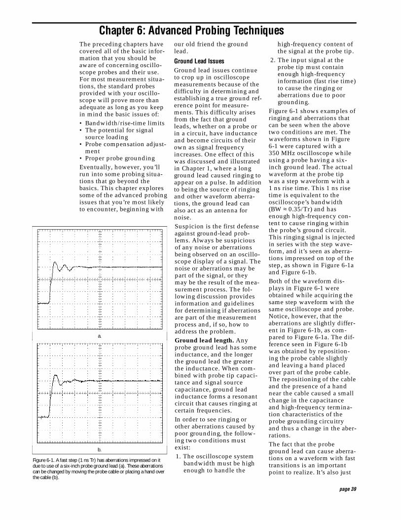
page 39
The preceding chapters havecovered all of the basic infor-mation that you should beaware of concerning oscillo-scope probes and their use.For most measurement situa-tions, the standard probesprovided with your oscillo-scope will prove more thanadequate as long as you keepin mind the basic issues of:
• Bandwidth/rise-time limits• The potential for signal
source loading• Probe compensation adjust-
ment• Proper probe grounding
Eventually, however, you’llrun into some probing situa-tions that go beyond thebasics. This chapter exploressome of the advanced probingissues that you’re most likelyto encounter, beginning with
our old friend the groundlead.
Ground Lead IssuesGround lead issues continueto crop up in oscilloscopemeasurements because of thedifficulty in determining andestablishing a true ground ref-erence point for measure-ments. This difficulty arisesfrom the fact that groundleads, whether on a probe orin a circuit, have inductanceand become circuits of theirown as signal frequencyincreases. One effect of thiswas discussed and illustratedin Chapter 1, where a longground lead caused ringing toappear on a pulse. In additionto being the source of ringingand other waveform aberra-tions, the ground lead canalso act as an antenna fornoise.
Suspicion is the first defenseagainst ground-lead prob-lems. Always be suspiciousof any noise or aberrationsbeing observed on an oscillo-scope display of a signal. Thenoise or aberrations may bepart of the signal, or theymay be the result of the mea-surement process. The fol-lowing discussion providesinformation and guidelinesfor determining if aberrationsare part of the measurementprocess and, if so, how toaddress the problem.
Ground lead length. Anyprobe ground lead has someinductance, and the longerthe ground lead the greaterthe inductance. When com-bined with probe tip capaci-tance and signal sourcecapacitance, ground leadinductance forms a resonantcircuit that causes ringing atcertain frequencies.
In order to see ringing orother aberrations caused bypoor grounding, the follow-ing two conditions mustexist:
1. The oscilloscope systembandwidth must be highenough to handle the
high-frequency content ofthe signal at the probe tip.
2. The input signal at theprobe tip must containenough high-frequencyinformation (fast rise time)to cause the ringing oraberrations due to poorgrounding.
Figure 6-1 shows examples ofringing and aberrations thatcan be seen when the abovetwo conditions are met. Thewaveforms shown in Figure6-1 were captured with a350 MHz oscilloscope whileusing a probe having a six-inch ground lead. The actualwaveform at the probe tipwas a step waveform with a1 ns rise time. This 1 ns risetime is equivalent to theoscilloscope’s bandwidth(BW ≈ 0.35/Tr) and hasenough high-frequency con-tent to cause ringing withinthe probe’s ground circuit.This ringing signal is injectedin series with the step wave-form, and it’s seen as aberra-tions impressed on top of thestep, as shown in Figure 6-1aand Figure 6-1b.
Both of the waveform dis-plays in Figure 6-1 wereobtained while acquiring thesame step waveform with thesame oscilloscope and probe.Notice, however, that theaberrations are slightly differ-ent in Figure 6-1b, as com-pared to Figure 6-1a. The dif-ference seen in Figure 6-1bwas obtained by reposition-ing the probe cable slightlyand leaving a hand placedover part of the probe cable.The repositioning of the cableand the presence of a handnear the cable caused a smallchange in the capacitanceand high-frequency termina-tion characteristics of theprobe grounding circuitryand thus a change in the aber-rations.
The fact that the probeground lead can cause aberra-tions on a waveform with fasttransitions is an importantpoint to realize. It’s also just
Chapter 6: Advanced Probing Techniques
Figure 6-1. A fast step (1 ns Tr) has aberrations impressed on itdue to use of a six-inch probe ground lead (a). These aberrationscan be changed by moving the probe cable or placing a hand overthe cable (b).
b.
a.

page 40
as important to realize thataberrations seen on a wave-form might just be part of thewaveform and not a result ofthe probe grounding method.To distinguish between thetwo situations, move theprobe cable around. If plac-ing your hand over the probeor moving the cable causes achange in the aberrations, theaberrations are being causedby the probe grounding sys-tem. A correctly grounded(terminated) probe will becompletely insensitive tocable positioning or touch.
To further illustrate theabove points, the same wave-form was again acquired withthe same oscilloscope andprobe. Only this time, thesix-inch probe ground leadwas removed, and the stepsignal was acquired throughan ECB-to-Probe Tip Adaptorinstallation (see Figure 6-2).The resulting display of theaberration-free step wave-form is shown in Figure 6-3.Elimination of the probe’sground lead and direct termi-nation of the probe in theECB-to-Probe Tip Adaptorhas eliminated virtually all ofthe aberrations from thewaveform display. The dis-play is now an accurate por-trayal of the step waveform atthe test point.
There are two main conclu-sions to be drawn from theabove examples. The first isthat ground leads should bekept as short as possiblewhen probing fast signals.The second is that productdesigners can ensure highereffectiveness of productmaintenance and trou-bleshooting by designing inproduct testability. Thisincludes using ECB-to-ProbeTip Adaptors where neces-sary to better control the testenvironment and avoid mis-adjustment of product cir-cuitry during installation ormaintenance.
When you’re faced with mea-suring fast waveforms wherean ECB-to-Probe Tip Adaptorhasn’t been installed, remem-ber to keep the probe groundlead as short as possible. Inmany cases, this can be doneby using special probe tipadaptors with integralgrounding tips. Yet anotheralternative is to use an activeFET probe. FET probes,because of their high inputimpedance and extremely lowtip capacitance (often lessthan 1 pF), can eliminatemany of the ground lead prob-lems often experienced withpassive probes. This is illus-trated further in Figure 6-4 .
Figure 6-3. The 1 ns rise time step waveform as acquired throughan ECB-to-Probe Tip Adaptor.
Figure 6-4. Examples of ground lead effects for passive probes versus active probes. The three traces on the left show the effects on the waveform of 1/2-inch,6-inch, and 12-inch ground leads used on a passive probe. The three traces on the right show the same waveform acquired using the same ground leads, butwith an active FET probe.
Figure 6-2. Typical ECB-to-Probe Tip Adaptor installation.

page 41
will flow. However, if thescope and test circuit are ondifferent building systemgrounds, there could be smallvoltage differences or noiseon one of the building groundsystems (see Figure 6-5). Theresulting current flow willdevelop a voltage drop acrossthe probe’s outer cable shield.This noise voltage will beinjected into the scope inseries with the signal fromthe probe tip. The result isthat you’ll see noise riding onthe signal of interest, or thesignal of interest may be rid-ing on noise.
With ground loop noise injec-tion, the noise is often linefrequency noise (60 Hz). Justas often, though, the noisemay be in the form of spikesor bursts resulting frombuilding equipment, such asair conditioners, switching onand off.
There are various things thatcan be done to avoid or mini-mize ground loop noise prob-lems. The first approach is tominimize ground loops byusing the same power circuitsfor the oscilloscope and cir-cuit under test. Additionally,the probes and their cablesshould be kept away fromsources of potential interfer-ence. In particular, don’tallow probe cables to lie
alongside or across equip-ment power cables.
If ground loop noise prob-lems persist, you may need toopen the ground loop by oneof the following methods:
1. Use a ground isolationmonitor.
2. Use a power line isolationtransformer on either thetest circuit or on thescope.
3. Use an isolation amplifierto isolate the scope probesfrom the scope.
4. Use differential probes tomake the measurement(rejects common-modenoise).
In no case should youattempt to isolate the oscillo-scope or test circuit by defeat-ing the safety three-wireground system. If it’s neces-sary to float the measure-ments, use an approved isola-tion transformer or preferablya ground isolation monitorspecifically designed for usewith an oscilloscope.
CAUTIONTo avoid electrical shock,always connect probes to theoscilloscope or probe isola-tor before connecting theprobe to the circuit undertest.
Induced noise. Noise canenter a common ground sys-tem by induction into probecables, particularly whenprobes with long cables areused. Proximity to powerlines or other current-carryingconductors can induce cur-rent flow in the probe’s outercable shield. The circuit iscompleted through the build-ing system common ground.To minimize this potentialsource of noise, use probeswith shorter cables when pos-sible, and always keep probecables away from possiblesources of interference.
Noise can also be induceddirectly into the probeground lead. This is theresult of typical probe groundleads appearing as a single-turn loop antenna when con-nected to the test circuit.This ground lead antenna is
Ground Lead Noise Prob-lems. Noise is another type ofsignal distortion that canappear on oscilloscope wave-form displays. As with ring-ing and aberrations, noisemight actually be part of thesignal at the probe tip, or itmight appear on the signal asa result of improper ground-ing techniques. The differ-ence is that the noise is gen-erally from an external sourceand its appearance is not afunction of the speed of thesignal being observed. Inother words, poor groundingcan result in noise appearingon any signal of any speed.
There are two primary mech-anisms by which noise can beimpressed on signals as aresult of probing. One is byground loop noise injection.The other is by inductivepickup through the probecable or probe ground lead.Both mechanisms are dis-cussed individually below.
Ground loop noise injection.Noise injection into thegrounding system can becaused by unwanted currentflow in the ground loop exist-ing between the oscilloscopecommon and test circuitpower line grounds and theprobe ground lead and cable.Normally, all of these pointsare, or should be, at zerovolts, and no ground current
Figure 6-5. The complete ground circuit, or ground loop, for an oscilloscope, probe, and test circuit on two differ-ent power plugs.
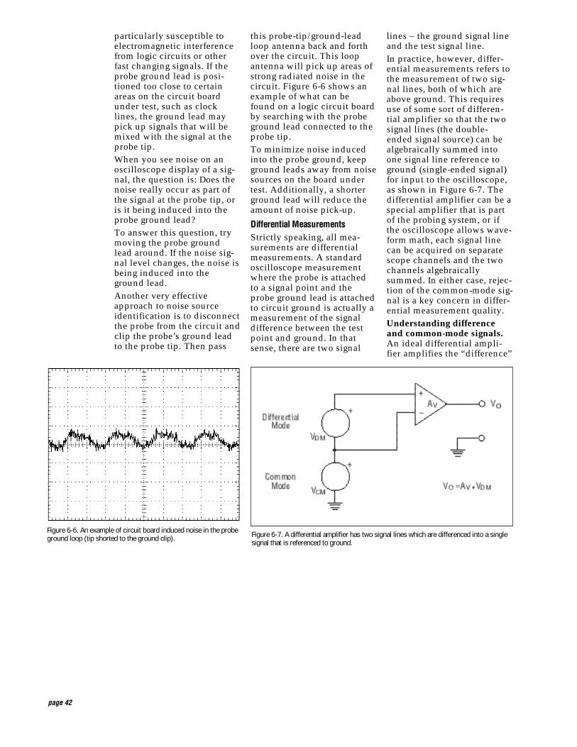
page 42
this probe-tip/ground-leadloop antenna back and forthover the circuit. This loopantenna will pick up areas ofstrong radiated noise in thecircuit. Figure 6-6 shows anexample of what can befound on a logic circuit boardby searching with the probeground lead connected to theprobe tip.
To minimize noise inducedinto the probe ground, keepground leads away from noisesources on the board undertest. Additionally, a shorterground lead will reduce theamount of noise pick-up.
Differential MeasurementsStrictly speaking, all mea-surements are differentialmeasurements. A standardoscilloscope measurementwhere the probe is attachedto a signal point and theprobe ground lead is attachedto circuit ground is actually ameasurement of the signaldifference between the testpoint and ground. In thatsense, there are two signal
lines – the ground signal lineand the test signal line.
In practice, however, differ-ential measurements refers tothe measurement of two sig-nal lines, both of which areabove ground. This requiresuse of some sort of differen-tial amplifier so that the twosignal lines (the double-ended signal source) can bealgebraically summed intoone signal line reference toground (single-ended signal)for input to the oscilloscope,as shown in Figure 6-7. Thedifferential amplifier can be aspecial amplifier that is partof the probing system, or ifthe oscilloscope allows wave-form math, each signal linecan be acquired on separatescope channels and the twochannels algebraicallysummed. In either case, rejec-tion of the common-mode sig-nal is a key concern in differ-ential measurement quality.
Understanding differenceand common-mode signals.An ideal differential ampli-fier amplifies the “difference”
particularly susceptible toelectromagnetic interferencefrom logic circuits or otherfast changing signals. If theprobe ground lead is posi-tioned too close to certainareas on the circuit boardunder test, such as clocklines, the ground lead maypick up signals that will bemixed with the signal at theprobe tip.
When you see noise on anoscilloscope display of a sig-nal, the question is: Does thenoise really occur as part ofthe signal at the probe tip, oris it being induced into theprobe ground lead?
To answer this question, trymoving the probe groundlead around. If the noise sig-nal level changes, the noise isbeing induced into theground lead.
Another very effectiveapproach to noise sourceidentification is to disconnectthe probe from the circuit andclip the probe’s ground leadto the probe tip. Then pass
Figure 6-7. A differential amplifier has two signal lines which are differenced into a singlesignal that is referenced to ground.
Figure 6-6. An example of circuit board induced noise in the probeground loop (tip shorted to the ground clip).

page 43
The voltage of interest, or dif-ference signal, is referred toas the differential voltage ordifferential mode signal andis expressed as:
VD Mwhere:
VDM = the V+in – V–in term in the equationa b o v e
Notice that the commonmode voltage, VCM, is not partof the above equation. That’s
because the ideal differentialamplifier rejects all of thecommon-mode component,regardless of its amplitude orfrequency.
Figure 6-8 provides an exam-ple of using a differentialamplifier to measure the gatedrive of the upper MOSFETdevice in an inverter circuit.As the MOSFET switches onand off, the source voltageswings from the positive sup-ply rail to the negative rail. Atransformer allows the gatesignal to be referenced to thesource. The differentialamplifier allows the scope tomeasure the true VG S signal (afew volt swing) at sufficientresolution, such as 2 V / d i v i-sion, while rejecting the sev-eral-hundred-volt transitionof the source to ground.
In real-life, differential ampli-fiers cannot reject all of thecommon-mode signal. Asmall amount of common-mode voltage appears as anerror signal in the output.This common-mode error sig-nal is indistinguishable fromthe desired differential signal.
The ability of a differentialamplifier to minimize unde-sirable common-mode signalsis referred to as common-mode rejection ratio or CMRRfor short. The true definitionof CMRR is “differential-mode gain divided by com-mon-mode gain referred tothe input”:
CMRR = AD M/ AC M
For evaluation purposes,CMRR performance can beassessed with no input sig-nal. The CMRR then becomesthe apparent VDM seen at theoutput resulting from thecommon-mode input. This isexpressed either as a ratio –such as 10,000:1 – or in dB:
dB = 20 log (AD M/ AC M)
For example, a CMRR of10,000:1 is equivalent to80 dB. To see the importanceof this, suppose you need tomeasure the voltage in theoutput damping resistor ofthe audio power amplifiershown in Figure 6-9. At fullload, the voltage across the
signal, VDM, between its twoinputs and completely rejectsany voltage which is commonto both inputs, VCM. Theresult is an output voltagegiven by:
VO – Av ( V+ i n - V- i n)
where:
Av = the amplifier’s gainVO = the output signal
referenced to earth ground
Figure 6-9. Common-mode error from a differential amplifier with 10,000:1 CMRR.
Figure 6-8. Differential amplifier used to measure gate to source voltage of upper transistor in an inverter bridge.Note that the source potential changes 350 volts during the measurement.

page 44
at the same frequency or fre-quencies.
It’s also important to realizethat CMRR specificationsassume that the common-mode component is sinu-soidal. This is often not thecase in real-life. For example,the common-mode signal inthe inverter of Figure 6-8 is a30 kHz square wave. Sincethe square wave containsenergy at frequencies consid-erably higher than 30 kHz,the CMRR will probably beworse than that specified atthe 30 kHz point.
Whenever the common-modecomponent is not sinusoidal,an empirical test is the quick-est way to determine theextent of the CMRR error (seeFigure 6-10). Temporarilyconnect both input leads tothe source. The scope is nowdisplaying only the common-mode error. You can nowdetermine if the magnitude ofthe error signal is significant.Remember, the phase differ-ence between VCM and VDM isnot specified. Therefore sub-tracting the displayed com-mon-mode error from the dif-ferential measurement willnot accurately cancel theerror term.
The test illustrated by Figure6-10 is handy for determiningthe extent of common-moderejection error in the actualmeasurement environment.However there’s one effectthis test will not catch. Withboth inputs connected to thesame point, there’s no differ-ence in driving impedance asseen by the amplifier. Thissituation produces the bestCMRR performance. Butwhen the two inputs of a dif-ferential amplifier are drivenfrom significantly differentsource impedances, theCMRR will be degraded.
Minimizing differential mea-surement errors. Connectingthe differential amplifier orprobe to the signal source isgenerally the greatest sourceof error. To maintain theinput match, both pathsshould be as identical as pos-sible. Any cabling should beof the same length for bothinputs.
If individual probes are usedfor each signal line, theyshould be the same modeland cable length. When mea-suring low-frequency signalswith large common-modevoltages, avoid the use ofattenuating probes. At highgains, they simply cannot beused as it’s impossible to pre-cisely balance their attenua-tion. When attenuation isneeded for high-voltage orhigh-frequency applications,special passive probesdesigned specifically for dif-ferential applications shouldbe used. These probes haveprovisions for precisely trim-ming DC attenuation and ACcompensation. To get the bestperformance, a set of probesshould be dedicated to eachspecific amplifier and cali-brated with that amplifierusing the procedure includedwith the probes.
Input cabling that’s spreadapart acts as a transformerwinding. Any AC magneticfield passing through theloop induces a voltage whichappears to the amplifierinput as differential and willbe faithfully summed into the
damper (VDM) should reach35 mV with an output swing(VCM) of 80 Vp-p. The differen-tial amplifier being used hasa CMRR specification of10,000:1 at 1 kHz. With theamplifier driven to full powerwith a 1 kHz sine wave, oneten thousandth of the com-mon-mode signal will erro-neously appear as VDM at theoutput of the differentialamplifier, which would be80 V/10,000 or 8 mV. The8 mV of residual common-mode signal represents up toa 22% error in the true 35 mVsignal!
It’s important to note that theCMRR specification is anabsolute value. It doesn’tspecify polarity or degrees ofphase shift of the error.Therefore, you cannot simplysubtract the error from thedisplayed waveform. Also,CMRR generally is highest(best) at DC and degradeswith increasing frequency ofVCM. Some differential ampli-fiers plot the CMRR specifica-tion as a function of fre-quency; others simply pro-vide CMRR specifications at afew key frequencies. In eithercase, it’s important in com-paring differential amplifiersor probes to be certain thatyour CMRR comparisons are
Figure 6-10. Empirical test for adequate common-mode rejection. Both inputs are driven from the same point.Residual common-mode appears at the output. This test will not catch the effect of differential source impedances.
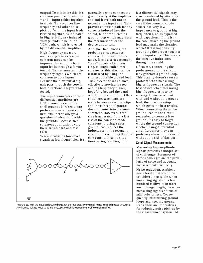
page 45
generally best to connect thegrounds only at the amplifierend and leave both uncon-nected at the input end. Thisprovides a return path for anycurrents induced into theshield, but doesn’t create aground loop which may upsetthe measurement or thedevice-under-test.
At higher frequencies, theprobe input capacitance,along with the lead induc-tance, forms a series resonant“tank” circuit which mayring. In single-ended mea-surements, this effect can beminimized by using theshortest possible ground lead.This lowers the inductance,effectively moving the res-onating frequency higher,hopefully beyond the band-width of the amplifier. Differ-ential measurements aremade between two probe tips,and the concept of grounddoes not enter into the mea-surement. However, if thering is generated from a fastrise of the common-modecomponent, using a shortground lead reduces theinductance in the resonantcircuit, thus reducing the ringcomponent. In some situa-tions, a ring resulting from
fast differential signals mayalso be reduced by attachingthe ground lead. This is thecase if the common-modesource has very lowimpedance to ground at highfrequencies, i.e. is bypassedwith capacitors. If this isn’tthe case, attaching the groundlead may make the situationworse! If this happens, trygrounding the probes togetherat the input ends. This lowersthe effective inductancethrough the shield.
Of course, connecting theprobe ground to the circuitmay generate a ground loop.This usually doesn’t cause aproblem when measuringhigher-frequency signals. Thebest advice when measuringhigh frequencies is to trymaking the measurementwith and without the groundlead; then use the setupwhich gives the best results.When connecting the probeground lead to the circuit,remember to connect it toground! It’s easy to forgetwhere the ground connectionis when using differentialamplifiers since they canprobe anywhere in the circuitwithout the risk of damage.
Small Signal MeasurementsMeasuring low-amplitudesignals presents a unique setof challenges. Foremost ofthese challenges are the prob-lems of noise and adequatemeasurement sensitivity.
Noise reduction. Ambientnoise levels that would beconsidered negligible whenmeasuring signals of a fewhundred millivolts or moreare no longer negligible whenmeasuring signals of tens ofmillivolts or less. Conse-quently, minimizing groundloops and keeping groundleads short are imperativesfor reducing noise pick up bythe measurement system. At
output! To minimize this, it’scommon practice to twist the+ and – input cables togetherin a pair. This reduces linefrequency and other noisepick up. With the input leadstwisted together, as indicatedin Figure 6-11, any inducedvoltage tends to be in theVCM path, which is rejectedby the differential amplifier.
High-frequency measure-ments subject to excessivecommon-mode can beimproved by winding bothinput leads through a ferritetorroid. This attenuates high-frequency signals which arecommon to both inputs.Because the differential sig-nals pass through the core inboth directions, they’re unaf-fected.
The input connectors of mostdifferential amplifiers areBNC connectors with theshell grounded. When usingprobes or coaxial input con-nections, there’s always aquestion of what to do withthe grounds. Because mea-surement applications vary,there are no hard and fastrules.
When measuring low-levelsignals at low frequencies, it’s
Figure 6-11. With the input leads twisted together, the loop area is very small, hence less field passes through it.Any induced voltage tends to be in the VCM path which is rejected by the differential amplifier.

page 46
Increasing measurement sen-sitivity. An oscilloscope’smeasurement sensitivity is afunction of it’s input cir-cuitry. The input circuitryeither amplifies or attenuatesthe input signal for an ampli-tude calibrated display of thesignal on the oscilloscopescreen. The amount of ampli-fication or attenuationneeded for displaying a signalis selected via the scope’svertical sensitivity setting,which is adjusted in terms ofvolts per display division(V/div).
In order to display and mea-sure small signals, the oscil-loscope input must haveenough gain or sensitivity toprovide at least a few divi-sions of signal display height.For example, to provide atwo-division high display of a20 mV peak-to-peak signal,the oscilloscope wouldrequire a vertical sensitivitysetting of 10 mV/div. For thesame two-division display ofa 10 mV signal, the highersensitivity setting of5 mV/div would be needed.Note that a low volts-per-division setting correspondsto high sensitivity and viceversa.
In addition to the require-ment of adequate oscillo-scope sensitivity for measur-ing small signals, you’ll alsoneed an adequate probe. Typ-ically, this will not be theusual probe supplied as astandard accessory with mostoscilloscopes. Standard
the extreme, power-line fil-ters and a shielded room maybe necessary for noise-freemeasurement of very lowamplitude signals.
However, before resorting toextremes, you should con-sider signal averaging as asimple and inexpensive solu-tion to noise problems. If thesignal you’re trying to mea-sure is repetitive and thenoise that you’re trying toeliminate is random, signalaveraging can provideextraordinary improvementsin the SNR (signal-to-noiseratio) of the acquired signal.An example of this is shownin Figure 6-12.
Signal averaging is a standardfunction of most digital stor-age oscilloscopes (DSOs). Itoperates by summing multi-ple acquisitions of the repeti-tive waveform and comput-ing an average waveformfrom the multiple acquisi-tions. Since random noisehas a long-term average valueof zero, the process of signalaveraging reduces randomnoise on the repetitive signal.The amount of improvementis expressed in terms of SNR.Ideally, signal averagingimproves SNR by 3 dB perpower of two averages. Thus,averaging just two waveformacquisitions (21) provides upto 3 dB of SNR improvement,averaging four acquisitions(22) provides 6 dB ofimprovement, eight averages(23) provides 9 dB ofimprovement, and so on.
Figure 6-12. A noisy signal (a) can be cleaned up by signal averag-ing (b).
b.
a.
NEW TERMSNR (signal-to-noise ratio) – Theratio of signal amplitude to noiseamplitude; usually expressed in dBas follows:
SNR = 20 log (Vs i g n a l / Vn o i s e )
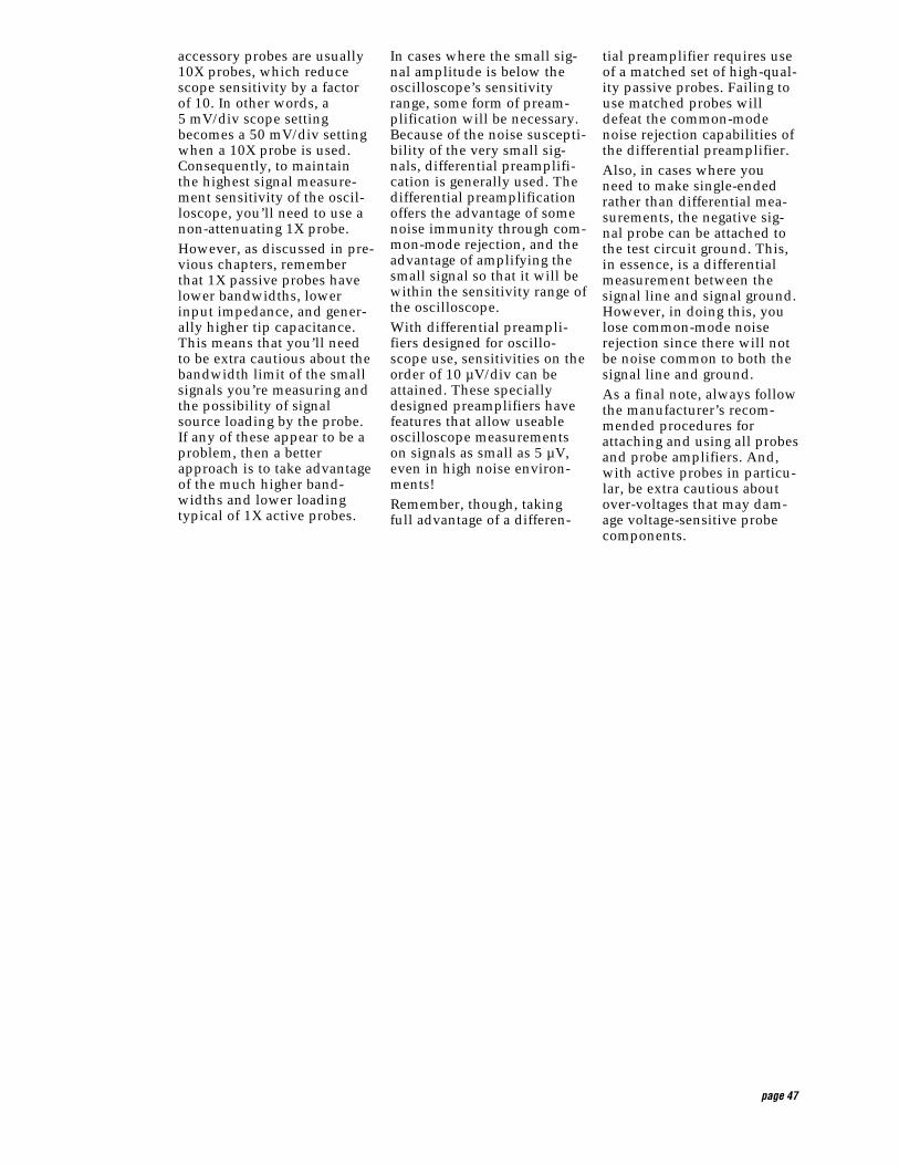
page 47
In cases where the small sig-nal amplitude is below theoscilloscope’s sensitivityrange, some form of pream-plification will be necessary.Because of the noise suscepti-bility of the very small sig-nals, differential preamplifi-cation is generally used. Thedifferential preamplificationoffers the advantage of somenoise immunity through com-mon-mode rejection, and theadvantage of amplifying thesmall signal so that it will bewithin the sensitivity range ofthe oscilloscope.
With differential preampli-fiers designed for oscillo-scope use, sensitivities on theorder of 10 µV/div can beattained. These speciallydesigned preamplifiers havefeatures that allow useableoscilloscope measurementson signals as small as 5 µV,even in high noise environ-ments!
Remember, though, takingfull advantage of a differen-
tial preamplifier requires useof a matched set of high-qual-ity passive probes. Failing touse matched probes willdefeat the common-modenoise rejection capabilities ofthe differential preamplifier.
Also, in cases where youneed to make single-endedrather than differential mea-surements, the negative sig-nal probe can be attached tothe test circuit ground. This,in essence, is a differentialmeasurement between thesignal line and signal ground.However, in doing this, youlose common-mode noiserejection since there will notbe noise common to both thesignal line and ground.
As a final note, always followthe manufacturer’s recom-mended procedures forattaching and using all probesand probe amplifiers. And,with active probes in particu-lar, be extra cautious aboutover-voltages that may dam-age voltage-sensitive probecomponents.
accessory probes are usually10X probes, which reducescope sensitivity by a factorof 10. In other words, a5 mV/div scope settingbecomes a 50 mV/div settingwhen a 10X probe is used.Consequently, to maintainthe highest signal measure-ment sensitivity of the oscil-loscope, you’ll need to use anon-attenuating 1X probe.
However, as discussed in pre-vious chapters, rememberthat 1X passive probes havelower bandwidths, lowerinput impedance, and gener-ally higher tip capacitance.This means that you’ll needto be extra cautious about thebandwidth limit of the smallsignals you’re measuring andthe possibility of signalsource loading by the probe.If any of these appear to be aproblem, then a betterapproach is to take advantageof the much higher band-widths and lower loadingtypical of 1X active probes.

page 48

page 49
• Check probe and test equip-ment documentation for,and observe any deratinginformation. For example,the maximum input voltagerating may decrease withincreasing frequency.
Use Proper GroundingProcedures• Probes are indirectly
grounded through thegrounding conductor of theoscilloscope power cord.To avoid electric shock, thegrounding conductor mustbe connected to earthground. Before making con-nections to the input or out-put terminals of the prod-uct, ensure that the productis properly grounded.
• Never attempt to defeat thepower cord grounds of anytest equipment.
• Connect probe ground leadsto earth ground only.
• Isolation of an oscilloscopefrom ground that is notspecifically designed andspecified for for this type ofoperation, or connecting aground lead to anythingother than ground couldresult in dangerous voltagesbeing present on the con-nectors, controls, or othersurfaces of the oscilloscopeand probes.
NOTEThis is true for most scopes,but there are some scopesthat are designed and speci-fied to operate in floatingapplications. An example isthe Tektronix THS700 Seriesbattery powered Digital Stor-age Oscilloscopes.
Connect and Disconnect ProbesProperly• Connect the probe to the
oscilloscope first. Thenproperly ground the probebefore connecting the probeto any test point.
• Probe ground leads shouldbe connected to earthground only.
• When disconnecting probesfrom the circuit under test,remove the probe tip fromthe circuit first, then dis-connect the ground lead.
• Except for the probe tip andthe probe connector centerconductor, all accessiblemetal on the probe (includ-ing the ground clip) is con-nected to the connectorshell.
Avoid Exposed Circuitry• Avoid touching exposed
circuitry or componentswith your hands or anyother part of your body.
• Make sure that probe tipsand ground lead clips areattached such that they donot accidentally brushagainst each other or otherparts of the circuit undertest.
Review the following safetyprecautions to avoid injuryand to prevent damage toyour test equipment or anyproduct that it is connectedto. To avoid potential haz-ards, use your test equipmentonly as specified by the man-ufacturer. Keep in mind thatall voltages and currents arepotentially dangerous, eitherin terms of personal hazard ordamage to equipment or both.
Observe All Terminal Ratings• To avoid fire or shock haz-
ard, observe all ratings andmarkings on the product.Consult the product manualfor further ratings informa-tion before making connec-tions to the product.
• Do not apply a potential toany terminal that exceedsthe maximum rating of thatterminal.
• Connect the ground lead ofprobes to earth groundonly.
NOTEFor those scopes that arespecifically designed andspecified to operate in afloating scope application(e.g., the Tektronix THS700Series battery powered Digi-tal Storage Oscilloscopes),the second lead is a com-mon lead and not a groundlead. In this case, follow themanufacturer’s specificationfor maximum voltage levelthat this can be connectedto.
Appendix A: Explanation of Safety Precautions

page 50
Do Not Operate Without Covers• Oscilloscopes and probes
should not be operatedwith any cover or protec-tive housing removed.Removing covers, shield-ing, probe bodies, or con-nector housings will exposeconductors or componentswith potentially hazardousvoltages.
Do Not Operate in Wet/DampConditions• To avoid electrical shock or
damage to equipment, donot operate measurementequipment in wet or dampconditions.
Do Not Operate in an ExplosiveAtmosphere• Operating electrical or elec-
tronic equipment in anexplosive atmosphere couldresult in an explosion.
Potentially explosive atmo-spheres may exist wherevergasoline, solvents, ether,propane, and other volatilesubstances are in use, havebeen in use, or are beingstored. Also, some finedusts or powders sus-pended in the air may pre-sent an explosive atmo-sphere.
Do Not Operate with SuspectedFailures• If you suspect there’s dam-
age, either electrical or phys-ical, to an oscilloscope orprobe, have it inspected byqualified service personnelbefore continuing usage.
Keep Probe Surfaces Clean andDry• Moisture, dirt, and other
contaminants on the probesurface can provide a con-ductive path. For safe andaccurate measurements,keep probe surfaces cleanand dry.
•Probes should be cleanedusing only the proceduresspecified in the probe’sdocumentation.
Do Not Immerse Probes inLiquids•Immersing a probe in a liq-
uid could provide a con-ductive path between inter-nal components or result indamage to or corrosion ofinternal components or theouter body and shielding.
•Probes should be cleanedusing only the proceduresspecified in the probe’sdocumentation.
Avoid RF Burns While HandlingProbes• To avoid RF (radio fre-
quency) burns, do not han-dle the probe leads whenthe leads are connected to asource that’s above the volt-age and frequency limitsspecified for RF burn risk(see Example DeratingCurve in Figure A-1).
• There’s always a risk of RFburns when using non-grounded probes and leadsets to measure signals, nor-mally above 300 volts and1 MHz.
• If you need to use a probewithin the risk area for RFburn, turn power off to thesource before connecting ordisconnecting the probeleads. Do not handle theinput leads while the cir-cuit is active.
Figure A-1. Example Derating Curve. Actual values and ranges will vary with specific products.

page 51
aberrations – Any deviationfrom the ideal or norm; usu-ally associated with the flattops and bases of waveformsor pulses. Signals may haveaberrations caused by the cir-cuit conditions of the signalsource, and aberrations maybe impressed upon a signalby the measurement system.In any measurement whereaberrations are involved, it isimportant to determinewhether the aberrations areactually part of the signal orthe result of the measurementprocess. Generally, aberra-tions are specified as a per-centage deviation from a flatresponse.
active probe – A probe con-taining transistors or otheractive devices as part of theprobe’s signal conditioningnetwork.
attenuation – The processwhereby the amplitude of asignal is reduced.
attenuator probe – A probethat effectively multiplies thescale factor range of an oscil-loscope by attenuating thesignal. For example, a 10Xprobe effectively multipliesthe oscilloscope display by afactor of 10. These probesachieve multiplication byattenuating the signal appliedto the probe tip; thus, a100 volt peak-to-peak signalis attenuated to 10 volts peak-to-peak by a 10X probe, andthen is displayed on theoscilloscope as a 100 voltspeak-to-peak signal through10X multiplication of thescope’s scale factor.
bandwidth – The continuousband of frequencies that anetwork or circuit passeswithout diminishing powermore than 3-dB from the mid-band power (refer to Figure1-5).
derate – To reduce the ratingof a component or systembased on one or more operat-ing variables; for example,amplitude measurementaccuracy may be deratedbased on the frequency of thesignal being measured.
distributed elements (L, R, C) –Resistance and reactance thatare spread out over the lengthof a conductor; distributedelement values are typicallysmall compared to lumpedcomponent values.
harmonics – Square waves,sawtooth waveforms, andother periodic non-sinusoidalwaveforms contain frequencycomponents that consist ofthe waveform’s fundamentalfrequency (1/period) and fre-quencies that are integer mul-tiples (1x, 2x, 3x, ...) of thefundamental which arereferred to as harmonic fre-quencies; the second har-monic of a waveform has afrequency that is twice that ofthe fundamental, the thirdharmonic frequency is threetimes the fundamental, andso on.
impedance – The process ofimpeding or restricting ACsignal flow. Impedance isexpressed in Ohms and con-sists of a resistive component(R) and a reactive component(X) that can be either capaci-tive (XC) or inductive (XL).Impedance (Z) is expressed ina complex form as:
Z = R + jX
or as a magnitude and phase,where the magnitude (M) is:
M = R2 + X2
and phase θ is:
θ = arctan(X/R)
linear phase – The character-istic of a network wherebythe phase of an applied sinewave is shifted linearly withincreasing sine wave fre-quency; a network with linearphase shift maintains the rel-ative phase relationships ofharmonics in non-sinusoidalwaveforms so that there’s nophase-related distortion inthe waveform.
load – The impedance that’splaced across a signal source;an open circuit would be a“no load” situation.
loading – The processwhereby a load applied to asource draws current fromthe source.
passive probe – A probewhose network equivalentconsists only of resistive (R),inductive (L), or capacitive(C) elements; a probe thatcontains no active compo-nents.
phase – A means of express-ing the time-related positionsof waveforms or waveformcomponents relative to a ref-erence point or waveform.For example, a cosine waveby definition has zero phase,and a sine wave is a cosinewave with 90-degrees ofphase shift.
probe power – Power that’ssupplied to the probe fromsome source such as theoscilloscope, a probe ampli-fier, or the circuit under test.Probes that require powertypically have some form ofactive electronics and, thus,are referred to as being activeprobes.
Appendix B: Glossary

page 52
source – The originationpoint or element of a signalvoltage or current; also, oneof the elements in a FET(field effect transistor).
source impedance – Theimpedance seen when look-ing back into a source.
time domain reflectometry(TDR) – A measurement tech-nique wherein a fast pulse isapplied to a transmissionpath and reflections of thepulse are analyzed to deter-mine the locations and typesof discontinuities (faults ormismatches) in the transmis-sion path.
trace ID – When multiplewaveform traces are dis-played on an oscilloscope, atrace ID feature allows a par-ticular waveform trace to beidentified as coming from aparticular probe or oscillo-scope channel. Momentarilypressing the trace ID buttonon a probe causes the corre-sponding waveform trace onthe oscilloscope to momen-tarily change in some manneras a means of identifying thattrace.
reactance – An impedanceelement that reacts to an ACsignal by restricting its cur-rent flow based on the signalsfrequency. A capacitor (C)presents a capacitive reac-tance to AC signals that isexpressed in Ohms by thefollowing relationship:
XC = 12πfC
where:XC = capacitive reactance in
Ohmsπ = 3.14159...f = frequency in HzC = capacitance in Farads
An inductor (L) presents aninductive reactance to AC sig-nals that’s expressed in Ohmsby the following relationship:
XL = 2πfLwhere:
XL = inductive reactance in Ohms
π = 3.14159....f = frequency in HzL = inductance in Henrys
readout – Alphanumericinformation displayed on anoscilloscope screen to pro-vide waveform scaling infor-mation, measurement results,or other information.
ringing – Oscillations thatresult when a circuit res-onates; typically, the dampedsinusoidal variations seen onpulses are referred to asringing.
rise time – On the rising tran-sition of a pulse, rise time isthe time it takes the pulse torise from the 10% amplitudelevel to the 90% amplitudelevel.
shielding – The practice ofplacing a grounded conduc-tive sheet of material betweena circuit and external noisesources so that the shieldingmaterial intercepts noise sig-nals and conducts them awayfrom the circuit.
SNR (signal-to-noise ratio) –The ratio of signal amplitudeto noise amplitude; usuallyexpressed in dB as follows:
SNR = 20 log (Vs i g n a l / Vn o i s e )

7/98 KC/XBS 60W–6053–7
Copyright © 1998, Tektronix, Inc. All rights reserved. Tektronix products are covered by U.S. and foreign patents, issued and pending. Information in thispublication supersedes that in all previously published material. Specification and price change privileges reserved. TEKTRONIX and TEK are registeredtrademarks of Tektronix, Inc. All other trade names referenced are the service marks, trademarks, or registered trademarks of their respective companies.
For further information, contact Tektronix:World Wide Web: http://www.tek.com; ASEAN Countries (65) 356-3900; Australia & New Zealand 61 (2) 9888-0100; Austria, Central Eastern Europe, Greece, Turkey, Malta,& Cyprus +43 2236 8092 0;Belgium +32 (2) 715 89 70; Brazil and South America 55 (11) 3741-8360;Canada 1 (800) 661-5625; Denmark +45 (44) 850 700; Finland +358 (9) 4783 400; France & North Africa +33 1 69 86 81 81; Germany + 49 (221) 94 77 400; Hong Kong (852) 2585-6688; India (91) 80-2275577; Italy +39 (2) 25086 501; Japan (Sony/Tektronix Corporation) 81 (3) 3448-3111;Mexico, Central America, & Caribbean 52 (5) 666-6333; The Netherlands +31 23 56 95555; Norway +47 22 07 07 00; People’s Republic of China 86 (10) 6235 1230; Republic of Korea 82 (2) 528-5299; South Africa (27 11)651-5222; Spain & Portugal +34 91 372 6000; Sweden +46 8 477 65 00 Switzerland +41 (41) 729 36 40; Taiwan 886 (2) 2722-9622; United Kingdom & Eire +44 (0)1628 403300; USA 1 (800) 426-2200.
From other areas, contact: Tektronix, Inc. Export Sales, P.O. Box 500, M/S 50-255, Beaverton, Oregon 97077-0001, USA 1 (503) 627-6877.