aboutdan sheingold [email protected] editor, analog dialogue. analog dialogue volume 33...
TRANSCRIPT


About Analog Dialogue
Analog Dialogue is the free technical magazine of Analog Devices, Inc., publishedcontinuously for thirty-three years, starting in 1967. It discusses products, applications,technology and techniques for analog, digital, and mixed-signal processing.
1www.analog.com/analogdialogue/2www.analog.com
Volume 33, the current issue, incorporates all articles published during 1999 in theWorld Wide Web1 editions. All recent issues, starting with Volume 29, Number 2(1995) have been archived on that website.
As one of the many informative Analog Devices publications, Analog Dialogue’sobjectives are to inform engineers, scientists, and electronic technicians about newADI products and technologies, and to help them understand and competentlyapply our products.
The monthly Web editions have at least three further objectives:
• Provide timely digests that alert readers to upcoming and available products.
• Provide a set of links to important and rapidly proliferating sourcesof information and activity fermenting within the ADI Web site.2
• Listen to reader suggestions and help find sources of aid to answertheir questions.
Thus, Analog Dialogue is more than a magazine: its links and tendrils to allparts of our website (and some outside sites) make its bookmark a favorite“high-pass-filtered” point of entry to the analog.com site—the world ofAnalog Devices.
Our hope is that readers will think of ADI publications as “Great Stuff” and theAnalog Dialogue bookmark on their web browser as a favorite alternative path toanswer the question, “What’s new at ADI?”
Welcome! Read and enjoy!
Dan [email protected], Analog Dialogue

Analog Dialogue Volume 33 (1999) 1
IN THIS ISSUEAnalog Dialogue Volume 33, 1999
PageEditor’s Notes, Authors . . . . . . . . . . . . . . . . . . . . . . . . . . . . . . . . . . . . . . . . . . . . . . . . . . . . . . . . 2
Othello: A new direct-conversion radio chip set eliminates IF stages . . . . . . . . . . . . . . . . . . . . . . . . . . . 3DSPs enhance flexible third-generation (3G) base station design . . . . . . . . . . . . . . . . . . . . . . . . . . . . . 6Phase-locked loops for high-frequency receivers and transmitters, Part 1 . . . . . . . . . . . . . . . . . . . . . . . . 9Phase-locked loops for high-frequency receivers and transmitters, Part 2 . . . . . . . . . . . . . . . . . . . . . . . 13Phase-locked loops for high-frequency receivers and transmitters, Part 3 . . . . . . . . . . . . . . . . . . . . . . . 18
Dual-axis, low-g, fully integrated accelerometers . . . . . . . . . . . . . . . . . . . . . . . . . . . . . . . . . . . . . . . 23Accelerometers—fantasy and reality (Ask The Applications Engineer—29) . . . . . . . . . . . . . . . . . . . . 25ADXL105: A lower-noise, wider-bandwidth accelerometer, rivals performance of
more expensive sensors . . . . . . . . . . . . . . . . . . . . . . . . . . . . . . . . . . . . . . . . . . . . . . . . . . . . . . 27
Logarithmic amplifiers explained (Ask The Applications Engineer—28) . . . . . . . . . . . . . . . . . . . . . . 30Analog-to-Digital converter architectures and choices for system design . . . . . . . . . . . . . . . . . . . . . . . . 35 New-Product Brief: AD9814 Low Power 14-Bit, 3-Channel CCD Signal Processor . . . . . . . . . 38 New-Product Brief: AD9884 8-bit, 140 MSPS Flat Panel Display Interface . . . . . . . . . . . . . . . 38New TxDAC® Generation: 125 MSPS 10-, 12-, and 14-bit high-performance DACs
for wideband multitone communication Transmit channels . . . . . . . . . . . . . . . . . . . . . . . . . . . . . . 39 New-Product Brief: AD9772 14-bit, 300 MSPS TxDAC . . . . . . . . . . . . . . . . . . . . . . . . . . . . . 40Ultrasound analog electronics primer . . . . . . . . . . . . . . . . . . . . . . . . . . . . . . . . . . . . . . . . . . . . . . 41
New-Product Brief: ADP3421 Geyserville-Enabled DC/DC Converter Controller . . . . . . . . . 43A chip you can use to monitor environmental conditions on PC motherboard designs . . . . . . . . . . . . . . 44Measuring Temperatures on Computer Chips with Speed and Accuracy: A new approach using
silicon sensors and off-chip processing . . . . . . . . . . . . . . . . . . . . . . . . . . . . . . . . . . . . . . . . . . . . 49 New-Product Brief: AD1881 AC’97 SoundMAX® Audio Codec . . . . . . . . . . . . . . . . . . . . . . . 53Compensate for loading effects on power lines with a DSP-controlled active shunt filter . . . . . . . . . . . . . 54Signal corruption in industrial measurement (Ask The Applications Enginee—27) . . . . . . . . . . . . . . . 58 New-Product Brief: AD8551/2/4 Zero-Drift, Single-Supply, Rail-to-Rail Op Amps . . . . . . . . . 59Process signals from millivolts to 610 V directly with a versatile single-supply 3/5 V
charge-balancing A/D converter . . . . . . . . . . . . . . . . . . . . . . . . . . . . . . . . . . . . . . . . . . . . . . . . 60 New-Product Brief: ADuC812 12-bit MicroConverter Data Acquisition System . . . . . . . . . . . 61Microcontroller-based energy metering using the AD7755 . . . . . . . . . . . . . . . . . . . . . . . . . . . . . . . . 62 New-Product Brief: ADMC401 DSP-Based High-Performance Motor Controller . . . . . . . . . . 63All-electronic power and energy meters . . . . . . . . . . . . . . . . . . . . . . . . . . . . . . . . . . . . . . . . . . . . . 64 New-Product Brief: AD7751 Fault-Tolerant Energy Metering IC . . . . . . . . . . . . . . . . . . . . . . 66Make vs. Buy: When should I re-invent the wheel? . . . . . . . . . . . . . . . . . . . . . . . . . . . . . . . . . . . . . 67
New ADI Fellows . . . . . . . . . . . . . . . . . . . . . . . . . . . . . . . . . . . . . . . . . . . . . . . . . . . . . . . . . . . . 70Authors (continued from page 2) . . . . . . . . . . . . . . . . . . . . . . . . . . . . . . . . . . . . . . . . . . . . . . . . 71Worth Reading: An authoritative, practical, readable new DSP book. Read it FREE on-line. . . . . 72
Cover: The cover illustration was designed and executed by Kristine Chmiel-Lafleur, of Communications Services, Analog Devices, Inc.

2 ISSN 0161–3626 Analog Dialogue Volume 33 © Analog Devices, Inc. 1999
Editor’s Notes1999: THE YEAR THAT WASIn 1999, with the aid of the WorldWide Web, Analog Dialogue hasincreased its value to its readers andsimultaneously increased its value toits sponsor, Analog Devices, Inc.With a target of monthly publica-tion, ten issues were published in1999, more than three times as manyas the yearly average over its prior 32 years in print. The greaterfrequency of publication made it possible for readers to read aboutnew products in timely fashion, and the ease of publishing on theWeb allowed us to literally “turn on a dime”. More importantly,though, it allowed readers immediately to link to extensive furtherinformation on products and topics of interest on the vast AnalogDevices Web Site and to promptly print usable data sheets. Thisessentially eliminated the need for Business Reply cards and thelengthy “circle and wait” cycle.
The one downside and source of anguish to many faithful readerswas that, in order to read Analog Dialogue, they had to access theWeb (a task that day by day is nevertheless becoming easier withthe help of some ADI broadband and DSL products). This issue,Volume 33, divorced from the quest for immediacy that energizesour Web version, is our answer to the need for a “permanent”version of Analog Dialogue that you can hold in your hand. Itcontains all the technical articles (and a few worthy New-ProductBriefs) that have been published during 1999. You can carry it,read it wherever you are (except in the dark), and stack it in abinder with previous issues to complete your set. And, in betweenthis edition and Volume 34, in December, 2000, you can still get up-to-date information from the monthly editions of ADI’s technicalmagazine on the Web.1 Surely this is the best of both worlds!
SCOTT WAYNEContributing EditorWe’re pleased to welcome ScottWayne to the staff of Analog Dialoguein the role of Contributing Editor.Scott is the newest addition to theCorporate Technical Communica-tions group at Analog Devices.
Besides contributing counsel andarticles to this publication, Scottworks with engineers at all levels and locations within AnalogDevices, with editors of trade publications, and with a wide rangeof technical people throughout the world to develop interestingand useful stories about designs, technologies, and applicationsof Analog Devices products. He also has a role in one of the moreimportant aspects of professional development—encouraging,stimulating, and helping engineers to overcome their reticence towrite technical articles.
Scott has an SBEE from MIT. He interned with Analog Devicesin 1978, and came back after graduating in 1979. Since then, hehas designed high-resolution analog-to-digital converters, digital-to-analog converters, sample-and-hold amplifiers, instrumentationamplifiers, isolation amplifiers, and an iontophoretic drug-deliverysystem using modular, hybrid, compound-monolithic, and
monolithic technologies. In June of 1999, Scott transferred out ofDesign, and into Corporate Marketing, where he is ADI’s SeniorTechnical Editor.
Scott has written articles and design ideas that have appeared inthe trade press, and he was a contributor to the 1986 edition ofthe Analog-Digital Conversion Handbook. He holds a patent for aprecision switched-capacitor-ratio system and has a second patentpending. He has presented several times at the Analog DevicesGeneral Technical Conference.
In his free time, Scott enjoys sailing, hiking, golf, bicycling,watching Boston’s Red Sox and Bruins, and hanging out with his“Little Brother,” Gary. [email protected] b
THE AUTHORSBrian Black (page 35), who joinedAnalog Devices in 1998, is ProductManager, high-resolution dataconverters, for the General-PurposeConverter group, in Wilmington, MA.He has a BSEE from Brigham YoungUniversity (1991), and MS degreesfrom MIT (1996) in both EE andManagement (Sloan School).
Michael Curtin (pages 9-22) is a StaffApplications Engineer at our Limerick,Ireland facility, providing applicationsupport for the frequency-synthesisproducts. Mike was graduated from theUniversity of Limerick with a BSc. Heis the author of several technicalarticles on high-resolution A/D and D/A converters and is the holder of twopatents. For relaxation, he enjoysplaying snooker, reading, and walking the family dog.
Robert De Robertis (page 6)manages the Wireless InfrastructureBusiness Group in ADI’s DSP division,which includes applications ofproducts such as TigerSHARC and theADSP-219x. His activities in the pastdecade have centered on leveragingDSP technologies into emerging digitalwireless markets. In his variousengineering, marketing, and product-line management positions at Analog Devices, Cadence DesignSystems, Lucent Technologies, and Harris Semiconductor, Robhas experienced many aspects of the wireless revolution.
Paul Daigle (page 64) joined AnalogDevices in 1997 as a Product Managerin the Standard Linear Products divi-sion. He holds an MSEE and BSEEfrom Syracuse University. Paul hasbeen participating in the semiconduc-tor industry since 1989. He thoroughlyenjoys life as father to a 1-year-old sonand a 3-year-old daughter. Mountainhikes and seaside walks are his family’sfavorites.
[more authors on Page 71]1http://www.analog.com/analogdialogue/
Analog Dialogue 33-10 (1999) 3
Othello: A New Direct-Conversion Radio ChipSet Eliminates IF Stagesby Dan Fague
INTRODUCTIONAnalog Devices recently announced the revolutionary Othellodirect-conversion radio for mobile applications. By eliminatingintermediate-frequency (IF) stages, this chip set will permit themobile electronics industry to reduce the size and cost of radiosections and enable flexible, multistandard, multimode operation.The radio consists of two integrated circuits, the AD6523 Zero-IF Transceiver and the AD6524 Multiband Synthesizer. TheAD6523 contains the main functions necessary for both a direct-conversion receiver and a direct VCO transmitter, known as theVirtual-IF™ transmitter. It also includes the local-oscillatorgeneration block and a complete on-chip regulator that suppliespower to all active circuitry for the radio. The AD6524 is afractional-N synthesizer that features extremely fast lock times toenable advanced data services over cellular telephones—such ashigh-speed circuit-switched data (HSCSD) and general packetradio services (GPRS).
Together, the two ICs supply the main functions necessary forimplementing dual- or triple-band radios for GSM cellular phones.The direct conversion technology, combined with a new twist onthe translation loop (or direct VCO) modulator, reduces theamount of external filtering needed in the radio to an absoluteminimum.
THE GSM STANDARDThe Global System for Mobiles (GSM) was officially launched in1992, after over five years of standards writing by the EuropeanTelecommunications Standards Institute (ETSI). The goal of GSMwas to unite a Babel of European communications under one digitalcellular standard. Before GSM, Europe maintained in effect oneseparate cellular network for each country, making internationalroaming on the continent virtually impossible. With GSM, a citizenof any of the original seventeen countries could roam to any othercountry using a single cellular handset. The standard, which waswritten with future expansion to data services and otherapplications in mind, soon became popular around the world. It isnow accepted in more than 140 countries, with over 200 networksrunning.
The frequency bands originally allocated to GSM were 890 to915 MHz for mobile transmitting and 935 to 960 MHz for mobilereceiving. That band was expanded to the so-called E-GSM bandsof 880 to 915 MHz and 925 to 960 MHz. Another frequencyallocation was made to further expand GSM capacity. This band,allocated to digital communications services (DCS), was 1710 to1785 MHz and 1805 to 1880 MHz. All countries adopting GSMuse one of these two pairs of frequency bands, except the UnitedStates, where both bands were already allocated by the FCC. ThePersonal Communications Services (PCS) frequency auctions inthe mid-1990s made available a set of bands for GSM in the U.S.—1850 to 1910 MHz and 1930 to 1990 MHz.
Today’s typical GSM handset (or handy) will have 2-W outputpower and is required to receive signals as low as –102 dBm (lessthan 1/10 of a picowatt). The handy includes a powerful digitalsignal processor (DSP) core (equivalent to an ADSP-218x) toencode, encrypt, interleave, packetize, transmit, receive, de-packetize, de-interleave, de-encrypt, and de-encode the data goingto and coming from the voiceband A/D and D/A converters. Anequally powerful microcontroller (ARM or Hitachi H8), combinedwith a hardware burst processor, controls the timing necessary toimplement the time-division multiple-access (TDMA) andfrequency hopping functions to keep the phone call on a specifictime and frequency channel. The microcontroller also implementsthe man-machine interface, and operates all the necessary protocolsfor communication to the base stations.
RADIO ARCHITECTURE DESIGNMost digital cellular phones today include at least one“downconversion” in their signal chain. This frequency conversionshifts the desired signal from the allocated RF band for the standard(say, at 900 MHz) to some lower intermediate frequency (IF),where channel selection is performed with a narrow channel-selectfilter (usually a surface acoustic-wave (SAW) or a ceramic type).The now-filtered signal is then further down-converted to either asecond IF or directly to baseband, where it is digitized anddemodulated in a digital signal processor (DSP).
The idea of using direct-conversion for receivers has long been ofinterest in RF design. The reason is obvious: in consumerequipment conversion stages add cost, bulk, and weight. Eachconversion stage requires a local oscillator, (often including afrequency synthesizer to lock the LO onto a given frequency), amixer, a filter, and (possibly) an amplifier. No wonder, then, thatdirect conversion receivers would be attractive. All intermediatestages are eliminated, reducing the cost, volume, and weight ofthe receiver.
The first Othello radio reduces the component count even moreby integrating the front-end GSM low-noise amplifier (LNA). Thiseliminates an RF filter (the “image” filter) that is necessary toeliminate the image, or unwanted mixing product of a mixer andthe off chip LNA. This stage, normally implemented with a discretetransistor, plus biasing and matching networks, accounts for a totalof about 12 components. Integrating the LNA saves a total of about15 to 17 components, depending on the amount of matching calledfor by the (now-eliminated) filter.
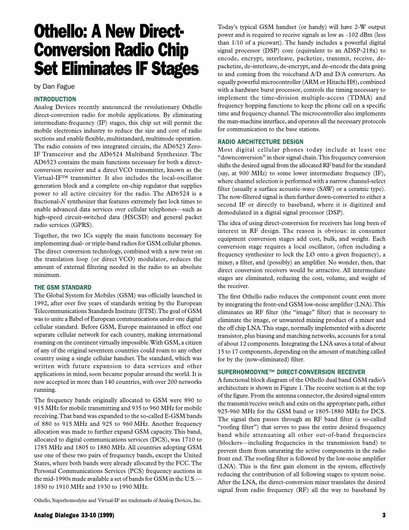
SUPERHOMODYNE™ DIRECT-CONVERSION RECEIVERA functional block diagram of the Othello dual band GSM radio’sarchitecture is shown in Figure 1. The receive section is at the topof the figure. From the antenna connector, the desired signal entersthe transmit/receive switch and exits on the appropriate path, either925-960 MHz for the GSM band or 1805-1880 MHz for DCS.The signal then passes through an RF band filter (a so-called“roofing filter”) that serves to pass the entire desired frequencyband while attenuating all other out-of-band frequencies(blockers—including frequencies in the transmission band) toprevent them from saturating the active components in the radiofront end. The roofing filter is followed by the low-noise amplifier(LNA). This is the first gain element in the system, effectivelyreducing the contribution of all following stages to system noise.After the LNA, the direct-conversion mixer translates the desiredsignal from radio frequency (RF) all the way to baseband by
Othello, Superhomodyne and Virtual-IF are trademarks of Analog Devices, Inc.

4 Analog Dialogue 33-10 (1999)
multiplying the desired signal with a local oscillator (LO) outputat the same frequency.
DAC
DAC
DIV N
ADC
ADC
LOGENERATIONVCO
PLL
AD6524
DIV MPHASEDETECTVCO
PA
SAW
SAW
T/RSWITCH
AD6523
O
Figure 1. Block diagram of the Othello dual-band radio.
The output of the mixer stage is then sent in quadrature (I and Qchannels) to the variable-gain baseband amplifier stage. The VGAalso provides some filtering of adjacent channels, and attenuationof in-band blockers. These blocking signals are other GSM channelsthat are some distance from the desired channel, say 3 MHz andbeyond. The baseband amplifiers filter these signals so that theywill not saturate the Receive ADCs. After the amplifier stage, thedesired signal is digitized by the Receive ADCs.
VIRTUAL-IF™ TRANSMITTERThe Transmit section begins on the right, at the multiplexed I andQ inputs/outputs. Because the GSM system is a time divisionduplex (TDD) system, the transmitter and receiver are never onat the same time. The Othello radio architecture takes advantageof this fact to save four pins on the transceiver IC’s package. Thequadrature transmit signals enter the transmitter through themultiplexed I/Os. These I and Q signals are then modulated ontoa carrier at an intermediate frequency greater than 100 MHz.
The output of the modulator goes to a phase-frequency detector(PFD), where it is compared to a reference frequency that isgenerated from the external channel selecting LO. The output ofthe PFD is a charge pump, operating at above 100 MHz, whoseoutput is filtered by a fairly wide (1 MHz) loop filter. The outputof the loop filter drives the tuning port of a voltage-controlledoscillator (VCO), with frequency ranges that cover the GSM andDCS transmit bands.
The output of the transmit VCO is sent to two places. The mainpath is to the transmit power amplifier (PA), which amplifies thetransmit signal from about +3 dBm to +35 dBm, sending it to thetransmit/receive switch and low-pass filter (which attenuates power-amplifier harmonics). The power amplifiers are dual band, with asimple CMOS control voltage for the band switch. The VCO outputalso goes to the transmit feedback mixer by means of a coupler,which is either a printed circuit, built with discrete inductors andcapacitors, or a monolithic (normally ceramic) coupling device.The feedback mixer downconverts the transmit signal to thetransmit IF, and uses it as the local oscillator signal for the transmitmodulator.
This type of modulator has several names, but the most descriptiveis probably “translation loop.” The translation loop modulator takes
advantage of one key aspect of the GSM standard: the modulationscheme is Gaussian-filtered minimum-shift keying (GMSK). Thistype of modulation does not affect the envelope amplitude, whichmeans that a power amplifier can be saturated and still not distortthe GMSK signal sent through it.
GMSK can be generated in several different ways. In anotherEuropean standard (for cordless telephones), GMSK is createdby directly modulating a free running-VCO with the Gaussianfiltered data stream. In GSM, the method of choice has beenquadrature modulation. Quadrature modulation creates accuratephase GMSK, but imperfections in the modulator circuit (or up-conversion stages) can produce envelope fluctuations, which canin turn degrade the phase trajectory when amplified by a saturatedpower amplifier. To avoid such degradations, GSM phone makershave been forced to use amplifiers with somewhat higher linearity,at the cost of reduced efficiency and talk time per battery chargecycle.
The translation loop modulator combines the advantages of directlymodulating the VCO and the inherently more accurate quadraturemodulation. In effect, the scheme creates a phase locked loop(PLL), comprising the modulator, the LO signal, and the VCOoutput and feedback mixer. The result is a directly modulated VCOoutput with a perfectly constant envelope and almost perfect phasetrajectory. Phase trajectory errors as low as 1.5 degrees have beenmeasured in the AD6523 transceiver IC, using a signal generatoras the LO signal to provide a reference for the loop.
FREQUENCY PLANNINGAn important aspect of the Othello radio design is the frequencyplan. The GSM standard has strict requirements with regard toin- and out-of-band spurious emissions. A GSM cellular phonemust be able to withstand blockers at extremely high levels (0 dBm)while continuing to receive normally. The phone must also notemit spurious signals into other bands above a certain level (in theGSM receive band, –112 dB relative to the transmitted signal!).
The Othello radio architecture was designed with the entire systemin mind. The frequency plan was carefully crafted to satisfy threeequally important criteria:
1) Reduce spurious emissions from the radio.
2) Minimize bandwidth of the dual band local oscillator (LO) VCO.
3) Eliminate as many potential blockers as possible.
By satisfying all of these criteria, major radio problems have beensolved, always keeping the end-user and the application in mind.The final solution turned out to be both elegant and practical.
Reducing Spurious Emissions from the RadioSpurious emissions from the radio can cause problems in bothTransmit and Receive modes. A wayward LO signal can find itsway to the antenna and “self block” a direct-conversion receiver,reducing sensitivity. The LO signal can also radiate from theantenna and degrade the performance of other receivers.
In the Othello frequency plan, the local oscillator’s center frequencywas chosen to be about 1350 MHz. This placed the LO strategicallybetween the GSM and DCS frequency bands, enabling a singleLO to be used for both GSM and DCS, saving components. Sincethat frequency is distant from either of the bands, the radio’s frontend filters will attenuate any radiated LO signal, and so it doesn’tpose a problem as a radiated spurious emission. Even if the signalis coupled directly from pin to pin on the IC, its power level would

Analog Dialogue 33-10 (1999) 5
be lower than the GSM requirements for in- or out-of-bandblockers received at the antenna.
In the Transmit section, spurious signals can also pose a problem.Though the transmitter is a direct VCO modulator, the feedbackmixer will introduce spurious signals at its output that must befiltered before entering the phase detector. Otherwise, they couldappear at the output themselves or cause still other spurious signalsto appear by mixing with the desired modulation signal due to thenon-linear operation of the phase detector input stage. This is aproblem inherent in any translation-loop modulator. By using awidely separated LO frequency, the Othello architecture simplifiesfiltering of these products.
Minimize Bandwidth of the Dual Band Local-Oscillator VCOThe Othello architecture was designed to minimize the numberof external components needed to build a complete dual-bandradio. The frequency plan was specifically chosen to make itpossible for a single LO VCO to cover both GSM and DCSfrequency bands while still meeting the necessarily stringent phase-noise specifications at the 3-MHz offset demanded of all GSMLO VCOs. By keeping the bandwidth requirements of the VCO toa minimum, the VCO can be designed with a maximum supplyvoltage of 2.7 V. This allows the entire dual-band radio to run at2.7 V, reducing power consumption and enabling the use of nickel-cadmium (NiCd), nickel metal-hydride (NiMH), or lithium-ion(Li-ion) battery types.
Eliminate as Many Potential Blockers as PossibleAs a result of the direct-conversion receiver architecture, theOthello radio has fewer “trouble” channels for the blocking testsrequired by GSM. Superheterodyne receivers must always contendwith half-IF responses that are difficult to filter with RF filtersdue to the shape factors required. By going to direct conversionOthello eliminates the half-IF response.
PERFORMANCEOne of the key advantages of the Othello radio is that the reductionin the number of components needed to implement it does notengender performance sacrifices. In both the GSM and DCSbands, the Othello system noise figure allows for a productionmargin of about 6 dB from the required receiver sensitivity of–102 dBm. The transmitter provides a similar production margin,with phase trajectory errors of 2.5° rms, compared with therequirement of 5° rms.
FUTURE BENEFITSAnother important feature of the Othello radio is that the AD6524’sfractional-N synthesizer has a lock time short enough to enableGPRS operation. [GPRS, an extension to the GSM networkcoming in year 2000, will allow very high data rates to be used bya compliant GSM handset.] A requirement of GPRS operation isthat the LO synthesizer must lock in less than half a GSM timeslot (lock times less than 250 µs). The AD6524, with its fractional-N synthesizer, is able to reach lock faster than conventionalsynthesizers, because fractional-N types operate at referencefrequencies that are higher than the channel spacing, thus jumpingmore than one channel per reference cycle. In the case of theAD6524, the 26-MHz reference frequency, twice the system crystalfrequency (compared to a channel spacing of 200 kHz), ensuresthat the Othello radio will meet the required lock time for GPRS.Fast lock time also helps to reduce power consumption by allowingthe baseband section to keep the radio off for longer time intervals.
The Othello radio has opened new doors of opportunity for thefuture. Today, a complete dual-band Othello radio, including allpower-management functions, can be implemented with only 90components. With so few components, the radio can beimplemented in less than 10 cm2 of board space. Figure 2 is aphotograph of a prototype radio design for Othello, implementedon a four layer PCB. Compare this to a superheterodyne receiverthat today uses about 225 components crowded into somewhatless than 15 cm2 of board space for the same functionality. (Eventhat is an improvement over radios of just two years ago, whichused the same number of components to implement a single bandGSM radio!) The advantages of direct conversion translate directlyto lower costs in many ways: fewer components means that anoriginal-equipment manufacturer (OEM) spends less on bill ofmaterials (BOM) and less for inserting the components (about apenny per insertion). The time to assemble a phone is reduced,increasing factory throughput; and the improved manufacturabilityof the phone (less to go wrong with fewer solder joints, etc.)increases reliability.
Figure 2. Photograph of a prototype Othello radio printedcircuit board.
Because Othello radios can be so compact, they enable GSM radiotechnology to be incorporated in many products from which ithas been excluded, such as very compact phones or PCMCIAcards. However, the real power of direct conversion will be seenwhen versatile third-generation phones are designed to handlemultiple standards. With direct-conversion, hardware channel-selection filters will be unnecessary, because channel selection isperformed in the digital signal-processing section, which can beprogrammed to handle multiple standards. Contrast this with thesuperheterodyne architecture; the multiple radio circuits requiredto handle the different standards (because each will requiredifferent channel-selection filters) will all have to be crowded intoa small space. With direct conversion, the same radio chain couldin concept be used for several different standards, bandwidths,and modulation types. Thus, Web-browsing and voice servicescould, in concept, occur over the GSM network using the sameradio in the handset.
ANALOG DEVICES AND GSMFor the future, the Othello radio is only the first of a family ofdirect-conversion receiver solutions from Analog Devices. Moreare in the works. But this technology is well-grounded in nearly adecade of product designs for the GSM industry. ADI chips canbe found in millions of GSM handsets in use worldwide. b

6 Analog Dialogue 33-10 (1999)
DSPs Enhance FlexibleThird-Generation Base-Station Designby Robert B. De Robertis and Rasekh Rifaat1
Designers are working on the third generation of cellular infrastructureequipment. This new equipment will give the service providerhigher user capacity (translates to more revenue), but moreimportantly, the consumer gets access to high-speed data services,including wireless Internet access and wireless video transmission.With target data rates of 2 megabits per second, standards for thisgeneration are in the process of being completed by the 3rd
Generation Partnership Project (3GPP). Ability to deliver flexiblesystems is the critical key for equipment manufacturers to win inthis market. Today’s proposals talk of achieving 2 MB/s data rates,but what about the 10-MB/s data rates of tomorrow? Flexibledesigns will enable the systems that are deployed to grow with thedemands of the consumer and the needs of the service provider.
Such flexibility in system design is of financial importance to serviceproviders because it extends the time during which theirinvestments in equipment are paying off. Over time, systems thatare programmable and scalable with minimal board replacementreduce the total capital outlay for new services. In turn, equipmentmanufacturers reduce their overall engineering costs in systemsthat are flexible and scalable to meet the future demands of theservice providers—the demand for continually increasedcapabilities at lower cost.
To the design engineer, flexibility means many things, includingconsideration of new technologies. The heart of the 3G systems israw signal processing, both analog and digital. Technologies andtechniques, such as direct intermediate-frequency (IF) sampling,direct digital down conversion, digital signal processing, and re-configurable logic, enable more flexible base station design optionstoday than were available for second-generation (2G) systems.Using them, the design engineer can create infrastructureequipment that has the flexibility to support the needs of serviceproviders, and has the performance and throughput to be scalableas infrastructure demand grows.
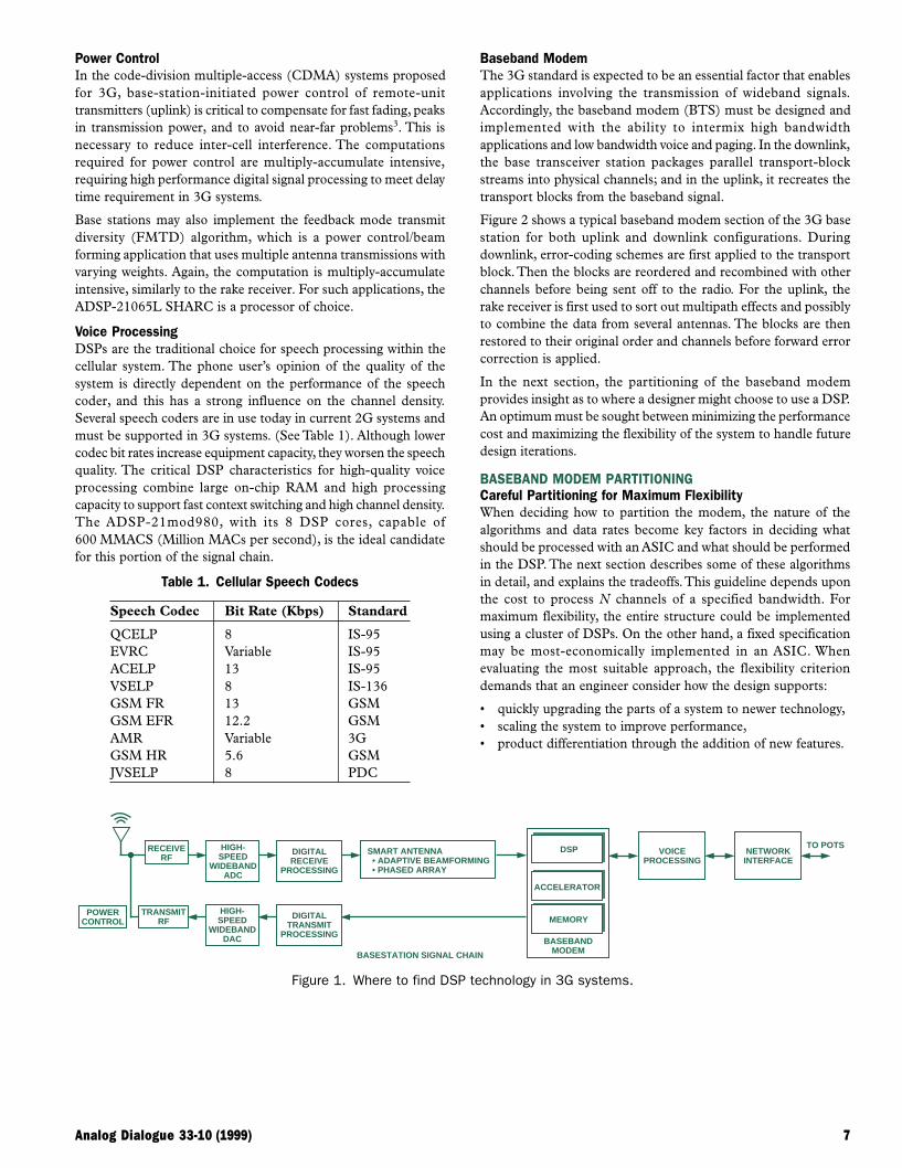
DSPs ARE ABUNDANT WITHIN THE 3G SYSTEMKey base-station areas that require high-performance DSPsinclude:• Antenna Arrays with Adaptive Digital Beam-Forming (BS)• Power Control (BS)• Voice Processing (BSC: Base-Station Control)• Baseband Modem (BTS: Base Transceiver Station)
The algorithms employed in these functional blocks are MAC-intensive (i.e., they employ many steps of multiply-and-accumulate).MAC-intensive functions for 3G include FIR, correlation, and
equalizer functions. The more rapidly these algorithms areperformed, the better the quality and performance of a base station
The choice of a DSP to obtain the required computation speed isnot a straightforward matter of specifying the highest clock speed.Architecture and instruction sets greatly affect the speed ofalgorithm execution. “MIPS” (millions of instructions per second)is also not a valid measure, since each manufacturer countsinstructions differently. A highly useful recommended measure,more closely related to algorithm execution, is the peak million-multiply-accumulates-per-second (MMACS). This calculation is theproduct of the clock speed and the number of MACs the DSP iscapable of executing per clock cycle2.
Another aspect to consider is the class of DSP architectureemployed. Two recently introduced new classes to consider are:very long instruction word (VLIW) and static superscalar.
VLIW attempts to reduce cost and increase execution speed byreducing hardware complexity. The sequencing mechanism inVLIW relies on an instruction format wherein every singleexecution unit in the chip is under direct programmer or compilercontrol. Unfortunately, VLIW has little or no hardware supportfor maintaining the integrity of data dependencies or avoidingscheduling hazards associated with real-time processing. In VLIW,all operation latencies in a particular implementation are fullyexposed to software. The TMS320C6x series from TexasInstruments is an example of a VLIW architecture.
Static superscalar architectures enforce a consistent and functionallywell-defined programming model, and the schedule is determinedprior to run time. It incorporates static scheduling techniques likethose found in VLIW, but it retains many superscalar and RISCattributes, enabling real time systems. Consequently, code can bewritten directly in assembly without requiring sophisticated timingprediction. The TigerSHARC™ DSP from Analog Devices is anexample of a static superscalar architecture.
Antenna Arrays with Adaptive Digital Beam FormingDigital beam-forming algorithms are designed to target sourcelocations in a noisy environment. They rapidly compare responsesof several spatially deployed antennas; the result of the computationis a signal that is believed to have originated from the targetdirection. Basically, they compute a correlation function thatcompares the signals and gives a measure of how close the desiredand received signals are. Due to the many factors involved in thealgorithm, and their wide dynamic range, floating point multiply-accumulate operations are used almost exclusively to minimizeroundoff errors.
The target is mobile, and could be moving at a significant speed,this adds another dimension of complexity to the computation.Adaptive beam-forming makes use of additional information tocontinually track the mobile target. Beam-forming in 3G systemsmay be integrated with the Rake receiver, where the signal isoperated on to combat fading and multipath effects. For thesealgorithms, the TigerSHARC’s rapid performance of floating-pointcomputations makes it an excellent fit.
TigerSHARC is a trademark of Analog Devices, Inc.1Much of the material in this article first appeared in Wireless System Design,published by Penton Media, Inc., October, 1999, and in their Web version,http://www.wsdmag.com/, November, 1999.
2D. Efstathiou et al., “Recent Developments in Enabling Technologies for Soft-ware Defined Radio,” IEEE Communications magazine, Aug., 1999.
3RT. Ojanpera, Wideband CDMA for Third Generation Mobile Communications,Boston-London: Artech House, 1998.
Analog Dialogue 33-10 (1999) 7
Power ControlIn the code-division multiple-access (CDMA) systems proposedfor 3G, base-station-initiated power control of remote-unittransmitters (uplink) is critical to compensate for fast fading, peaksin transmission power, and to avoid near-far problems3. This isnecessary to reduce inter-cell interference. The computationsrequired for power control are multiply-accumulate intensive,requiring high performance digital signal processing to meet delaytime requirement in 3G systems.
Base stations may also implement the feedback mode transmitdiversity (FMTD) algorithm, which is a power control/beamforming application that uses multiple antenna transmissions withvarying weights. Again, the computation is multiply-accumulateintensive, similarly to the rake receiver. For such applications, theADSP-21065L SHARC is a processor of choice.
Voice ProcessingDSPs are the traditional choice for speech processing within thecellular system. The phone user’s opinion of the quality of thesystem is directly dependent on the performance of the speechcoder, and this has a strong influence on the channel density.Several speech coders are in use today in current 2G systems andmust be supported in 3G systems. (See Table 1). Although lowercodec bit rates increase equipment capacity, they worsen the speechquality. The critical DSP characteristics for high-quality voiceprocessing combine large on-chip RAM and high processingcapacity to support fast context switching and high channel density.The ADSP-21mod980, with its 8 DSP cores, capable of600 MMACS (Million MACs per second), is the ideal candidatefor this portion of the signal chain.
Table 1. Cellular Speech Codecs
Speech Codec Bit Rate (Kbps) Standard
QCELP 8 IS-95EVRC Variable IS-95ACELP 13 IS-95VSELP 8 IS-136GSM FR 13 GSMGSM EFR 12.2 GSMAMR Variable 3GGSM HR 5.6 GSMJVSELP 8 PDC
Baseband ModemThe 3G standard is expected to be an essential factor that enablesapplications involving the transmission of wideband signals.Accordingly, the baseband modem (BTS) must be designed andimplemented with the ability to intermix high bandwidthapplications and low bandwidth voice and paging. In the downlink,the base transceiver station packages parallel transport-blockstreams into physical channels; and in the uplink, it recreates thetransport blocks from the baseband signal.
Figure 2 shows a typical baseband modem section of the 3G basestation for both uplink and downlink configurations. Duringdownlink, error-coding schemes are first applied to the transportblock. Then the blocks are reordered and recombined with otherchannels before being sent off to the radio. For the uplink, therake receiver is first used to sort out multipath effects and possiblyto combine the data from several antennas. The blocks are thenrestored to their original order and channels before forward errorcorrection is applied.
In the next section, the partitioning of the baseband modemprovides insight as to where a designer might choose to use a DSP.An optimum must be sought between minimizing the performancecost and maximizing the flexibility of the system to handle futuredesign iterations.
BASEBAND MODEM PARTITIONINGCareful Partitioning for Maximum FlexibilityWhen deciding how to partition the modem, the nature of thealgorithms and data rates become key factors in deciding whatshould be processed with an ASIC and what should be performedin the DSP. The next section describes some of these algorithmsin detail, and explains the tradeoffs. This guideline depends uponthe cost to process N channels of a specified bandwidth. Formaximum flexibility, the entire structure could be implementedusing a cluster of DSPs. On the other hand, a fixed specificationmay be most-economically implemented in an ASIC. Whenevaluating the most suitable approach, the flexibility criteriondemands that an engineer consider how the design supports:
• quickly upgrading the parts of a system to newer technology,• scaling the system to improve performance,• product differentiation through the addition of new features.
RECEIVERF
HIGH-SPEED
WIDEBANDDAC
HIGH-SPEED
WIDEBANDADC
BASESTATION SIGNAL CHAIN
TRANSMITRF
POWERCONTROL
DIGITALTRANSMIT
PROCESSING
SMART ANTENNA • ADAPTIVE BEAMFORMING • PHASED ARRAY
DSP
ACCELERATOR
MEMORY
VOICEPROCESSING
NETWORKINTERFACE
DIGITALRECEIVE
PROCESSING
BASEBANDMODEM
TO POTS
Figure 1. Where to find DSP technology in 3G systems.

8 Analog Dialogue 33-10 (1999)
Rake, Channel-Encoding/Decoding Hardware-SoftwareTradeoffsFigure 2 shows different classifications for the different parts ofthe modem. Each of the blocks performs different types ofcomputations. An overview is needed in order to see exactly whereDSP is more appropriate than other alternatives.
The interleaving, channel segmenting, and rate matching are I/O-intensive operations, which combine data from several sources andreorganize data to minimize the effects of errors. Because of thevariability of the parameters, data-rates, and memory-referencing,these functions are ideally suited to DSP for manipulation; theywould be difficult to implement cost-effectively in an ASIC.
The error-coding and -correction algorithms involve significantbit manipulations that—properly implemented—can beimplemented in the DSP. The error-correction algorithms alsorepresent an area of the modem that can provide equipment-manufacturer differentiation. The encoding standards have beenfixed, while decoding is left to implementers to design using theirown intellectual property. Companies that have a strong ASICcapability might choose a hard-wired design, while others that arestrong in programming and desire flexibility will choose the DSPapproach. ADI’s TigerSHARC DSP provides all the processingcapacity to enable a single high speed 3G data channel.
3G systems, employing spread spectrum communications, willutilize CDMA spreading codes in order to provide greater useof available bandwidth. The spreading and despreadingalgorithms are multiply-accumulate intensive, but at extremelyhigh data rates. The rake receiver takes its name from the factthat its diagram resembles a garden rake. Each finger tries tocorrelate the incoming data with the expected spreading code.As a result, the rake receiver needs to be able to process K times
the determined bandwidth, where K is the number of fingers inthe rake. In addition to that, the receiver must operate at thefrequency set by the spreading codes.
DSP technology today doesn’t cost-effectively support thebandwidth required for the spreading and despreading in 3Gsystems. However, production systems will not be manu-factured and installed for several years, so there is everyincentive for this situation to change. A clear examination ofthe upgrade path and projected performance of DSPs may showthat, by the time these systems are deployed, these functionscan indeed be handled cost-effectively.
Glueless Homogeneous and Heterogeneous MultiprocessingRegardless of the technology used to implement each section ofthe baseband modem, a significant amount of data must be movedaround the system. In considering the design, components (orgroups of components) that support high-bandwidth communica-tions must be used. The TigerSHARC DSP provides several optionsfor high-speed communication, including on-chip DMA (directmemory-access) and SDRAM support, along with dedicated user-programmable link ports. In multiprocessing designs, a high speedcluster bus can be used to connect as many as eight TigerSHARCDSPs without additional logic.
CONCLUSIONDesigners of 3G base stations will make use of the DSPs in orderto achieve the high performance and flexibility needed fortomorrow’s voice and data applications. Flexibility at all levels willdrive the need for scalable technologies, such as static super scalararchitectures and glueless interconnection of system components.Effective embodiment of these design principles will fulfill thepromise of 3G to provide the foundations of the kind of wirelessinfrastructure necessary for tomorrow’s killer applications. b
ERRORCODING
FORWARDERROR
CORRECTION
CHANNEL SEGMENTATIONRATE MATCHINGINTERLEAVING
CHANNEL DESEGMENTATIONRATE DETECTIONDEINTERLEAVING
NETWORKINTERFACE
STRUCTUREDBIT OPERATIONS
WITH RIGIDPARAMETERS
MEMORY-INTENSIVEOPERATIONS
REQUIRING FLEXIBLEPARAMETERS
MAC-INTENSIVEOPERATIONSREQUIRINGVERY HIGH
BANDWIDTH
RADIOINTERFACE
UPLINK
DOWNLINKSPREADING
DESPREADING(RAKE RECEIVER)
Figure 2. Block diagram showing the baseband processor’s signal chain.

Analog Dialogue 33-3 (© 1999 Analog Devices) 9
Phase-Locked Loopsfor High-FrequencyReceivers andTransmitters—Part 1by Mark Curtin and Paul O’Brien
This 3-part series of articles is intended to give a comprehensiveoverview of the use of PLLs (phase-locked loops) in both wiredand wireless communication systems.
In this first part, the emphasis is on the introductory concepts ofPLLs. The basic PLL architecture and principle of operation isdescribed. We will also give an example of where PLLs are used incommunication systems. We will finish the first installment byshowing a practical PLL circuit using the ADF4111 FrequencySynthesizer and the VCO190-902T Voltage-ControlledOscillator.
In the second part, we will examine in detail the criticalspecifications associated with PLLs: phase noise, reference spursand output leakage current. What causes these and how can theybe minimized? What effect do they have on system performance?
The final installment will contain a detailed description of theblocks that go to make up a PLL synthesizer and the architectureof an Analog Devices synthesizer. There will also be a summary ofsynthesizers and VCOs currently available on the market, with alist of ADI’s current offerings.
PLL BASICSA phase-locked loop is a feedback system combining a voltage-controlled oscillator and a phase comparator so connected thatthe oscillator maintains a constant phase angle relative to areference signal. Phase-locked loops can be used, for example, togenerate stable output frequency signals from a fixed low-frequencysignal. The first phase-locked loops were implemented in the early1930s by a French engineer, de Bellescize. However, they onlyfound broad acceptance in the marketplace when integrated PLLsbecame available as relatively low-cost components in the mid-1960s.
The phase locked loop can be analyzed in general as a negative-feedback system with a forward gain term and a feedback term.
A simple block diagram of a voltage-based negative-feedbacksystem is shown in Figure 1.
G(s)
H(s)
Vi VO+
–
e(s)
Figure 1. Standard negative-feedback control system model.
In a phase-locked loop, the error signal from the phase comparatoris proportional to the relative phase of the input and feedbacksignals. The average output of the phase detector will be constantwhen the input and feedback signals are the same frequency. Theusual equations for a negative-feedback system apply.
Forward Gain = G(s), [s = jω = j2πf]Loop Gain = G(s) × H(s)
Closed Loop Gain
G s
G s H s− =
+
( )
( ) ( )1
Because of the integration in the loop, at low frequencies the steadystate gain, G(s), is high and
VO/VI, Closed-Loop Gain =
1
H
The components of a PLL that contribute to the loop gain include:
1. The phase detector (PD) and charge pump (CP).
2. The loop filter, with a transfer function of Z(s)
3. The voltage-controlled oscillator (VCO), with a sensitivity ofKV/s
4. The feedback divider, 1/N
N1
FREF( UREF )
FO( UO )
+
-
e(s)PD Kd Z(s) Kv
s
CP
Error Detector Loop Filter VCO
Feedback Divider
Figure 2. Basic phase-locked-loop model.
If a linear element like a four-quadrant multiplier is used as thephase detector, and the loop filter and VCO are also analogelements, this is called an analog, or linear PLL (LPLL).
If a digital phase detector (EXOR gate or J-K flip flop) is used,and everything else stays the same, the system is called a digitalPLL (DPLL).
If the PLL is built exclusively from digital blocks, without anypassive components or linear elements, it becomes an all-digitalPLL (ADPLL).
Finally, with information in digital form, and the availability ofsufficiently fast processing, it is also possible to develop PLLs inthe software domain. The PLL function is performed by softwareand runs on a DSP. This is called a software PLL (SPLL).
Referring to Figure 2, a system for using a PLL to generate higherfrequencies than the input, the VCO oscillates at an angularfrequency of ωO. A portion of this signal is fed back to the errordetector, via a frequency divider with a ratio 1/N. This divided-down frequency is fed to one input of the error detector. The otherinput in this example is a fixed reference signal. The error detectorcompares the signals at both inputs. When the two signal inputsare equal in frequency, the error will be constant and the loop issaid to be in a “locked” condition. If we simply look at the errorsignal, the following equations may be developed.

10 Analog Dialogue 33-3 (© 1999 Analog Devices)
∆ F
∆ V
VCO Tunin g Volta ge (Volts )
VC
O O
utpu
t Fre
quen
cy (
MH
z)
KV = ∆F/∆V
Figure 3. VCO transfer function.
The overall transfer function (CLG or Closed-Loop Gain) of thePLL can be expressed simply by using the CLG expression for anegative feedback system as given above.
F
F
Forward Gain
Loop Gain
O
REF
=+1
Forward Gain G
K K Z s
s
D V, =
( )
Loop Gain GH
K K Z s
Ns
D V, =
( )
When GH is much greater than 1, we can say that the closed looptransfer function for the PLL system is N and so
FOUT = N × FREF
The loop filter is a low-pass type, typically with one pole and onezero. The transient response of the loop depends on:
1. the magnitude of the pole/zero,
2. the charge pump magnitude,
3. the VCO sensitivity,
4. the feedback factor, N.
All of the above must be taken into account when designing theloop filter. In addition, the filter must be designed to be stable(usually a phase margin of π/4 is recommended). The 3-dB cutofffrequency of the response is usually called the loop bandwidth,BW. Large loop bandwidths result in very fast transient response.However, this is not always advantageous, as we shall see inPart 2, since there is a tradeoff between fast transient responseand reference spur attenuation.
PLL APPLICATIONS TO FREQUENCY UPSCALINGThe phase-locked loop allows stable high frequencies to begenerated from a low-frequency reference. Any system thatrequires stable high frequency tuning can benefit from thePLL technique. Examples of these applications includewireless base stations, wireless handsets, pagers, CATVsystems, clock-recovery and -generation systems. A goodexample of a PLL application is a GSM handset or base station.Figure 4 shows the receive section of a GSM base station.
In the GSM system, there are 124 channels (8 users per channel)of 200-kHz width in the RF band. The total bandwidth occupiedis 24.8 MHz, which must be scanned for activity. The handset hasa transmit (Tx) range of 880 MHz to 915 MHz and a receive (Rx)range of 925 MHz to 960 MHz. Conversely, the base station has aTx range of 925 MHz to 960 MHz and an Rx range of 880 MHzto 915 MHz. For this example, we will consider just the base stationtransmit and receive sections. The frequency bands for GSM900and DCS1800 Base Station Systems are shown in Table 1. Table 2shows the channel numbers for the carrier frequencies (RFchannels) within the frequency bands of Table 1. Fl(n) is the centerfrequency of the RF channel in the lower band (Rx) and Fu(n) isthe corresponding frequency in the upper band (Tx).
Table 1. Frequency Bands for GSM900 and DCS1800 BaseStation Systems
Tx Rx
P-GSM900 935 to 960 MHz 890 to 915 MHzDCS1800 1805 to 1880 MHz 1710 to 1785 MHzE-GSM900 925 to 960 MHz 880 to 915 MHz
Table 2. Channel Numbering for GSM900 and DCS1800 Base Station Systems
Rx Tx
PGSM900 Fl(n) = 890 + 0.2 × (n) 1 ≤ n ≤ 124 Fu(n) = Fl(n) + 45
EGSM900 Fl(n) = 890 + 0.2 × (n) 0 ≤ n ≤ 124 Fu(n) = Fl(n) + 45Fl(n) = 890 + 0.2 × (n – 1024) 975 ≤ n ≤ 1023
DCS1800 Fl(n) = 1710.2 + 0.2 × (n – 512) 512 ≤ n ≤ 885 Fu(n) = Fl(n) + 95
e sN
de s
dtF
F
N
REFO
REFO
( ) = −
( )= −
ΦΦ
When
e s cons t
F
NFO
REF( ) = =tan ,
Thus
F N FO REF=
In commercial PLLs, the phase detector and charge pump togetherform the error detector block. When FO ≠ N FREF, the error detectorwill output source/sink current pulses to the low-pass loop filter.This smooths the current pulses into a voltage which in turn drivesthe VCO. The VCO frequency will then increase or decrease asnecessary, by KV DV, where KV is the VCO sensitivity in MHz/Volt and DV is the change in VCO input voltage. This will continueuntil e(s) is zero and the loop is locked. The charge pump andVCO thus serves as an integrator, seeking to increase or decreaseits output frequency to the value required so as to restore its input(from the phase detector) to zero.

Analog Dialogue 33-3 (© 1999 Analog Devices) 11
The 900-MHz RF input is filtered, amplified and applied to thefirst stage mixer. The other mixer input is driven from a tunedlocal oscillator (LO). This must scan the input frequency range tosearch for activity on any of the channels. The actual implementa-tion of the LO is by means of the PLL technique already described.If the 1st intermediate-frequency (IF) stage is centered at240 MHz, then the LO must have a range of 640 MHz to 675 MHzin order to cover the RF input band. When a 200-kHz referencefrequency is chosen, it will be possible to sequence the VCO outputthrough the full frequency range in steps of 200 kHz. For example,when an output frequency of 650 MHz is desired, N will have avalue of 3250. This 650-MHz LO will effectively check the 890-MHz RF channel (FRF – FLO = FIF or FRF = FLO + FIF). When Nis incremented to 3251, the LO frequency will now be 650.2 MHzand the RF channel checked will be 890.2 MHz. This is showngraphically in Figure 5.
(N)FREF(N-1)FREF (N+1)FREF
GSM Example
∆F = FREF
For GSM: F REF = 200 kHz
FRF = 880MHz to 915MHz for the Receiver
If First IF is at 240MHz then LO must go from
640MHz to 675MHz.
This Means N must vary from 3200 to 3375
Figure 5. Testing frequencies for GSM base-station receiver.
900MHzRF
L0 1Tuned
1ST IF240 MHz
L0 2Fixed
2ND IF10.7 MHz
Demodulator
SynthesizerVCO Synthesizer VCO
TCXO 13MHz
–104dBm to –60dBm
640MHz to675MHz
229.3MHz
Figure 4. Signal chain for GMS base-station receiver.
On the transmit side of the GSM system, similar requirementsexist. However, it is more common to go directly from basebandto the final RF in the Transmit section; this means that the typicalTX VCO for a base station has a range of 925 MHz to 960 MHz(RF band for the Transmit section).
CIRCUIT EXAMPLEFigure 6 shows an actual implementation of the local oscillatorfor the transmit section of a GSM handset. We are assuming directbaseband to RF up-conversion. This circuit uses the new ADF4111PLL Frequency Synthesizer from ADI and the VCO190-902TVoltage Controlled Oscillator from Vari-L Corporation (http://www.vari-L.com/).
The reference input signal is applied to the circuit at FREFIN andis terminated in 50 Ω. This reference input frequency is typically13 MHz in a GSM system. In order to have a channel spacing of200 kHz (the GSM standard), the reference input must be dividedby 65, using the on-chip reference divider of the ADF4111.
The ADF4111 is an integer-N PLL frequency synthesizer, capableof operating up to an RF frequency of 1.2 GHz. In this integer-Ntype of synthesizer, N can be programmed from 96 to 262,000 indiscrete integer steps. In the case of the handset transmitter, wherean output range of 880 MHz to 915 MHz is needed, and wherethe internal reference frequency is 200 kHz, the desired N valueswill range from 4400 to 4575.
It is worth noting that, in addition to the tunable RF LO, thereceiver section also uses a fixed IF (in the example shown this is240 MHz). Even though frequency tuning is not needed on thisIF, the PLL technique is still used. The reason for this is that it isan affordable way of using the stable system reference frequencyto produce the high frequency IF signal. Several synthesizermanufacturers recognize this fact by offering dual versions of thedevices: one operating at the high RF frequency (>800 MHz) andone operating at the lower IF frequency (500 MHz or less).

12 Analog Dialogue 33-3 (© 1999 Analog Devices)
The charge pump output of the ADF4111 (Pin 2) drives the loopfilter. This filter (Z(s) in Figure 2) is basically a 1st-order lag-leadtype. In calculating the loop filter component values, a number ofitems need to be considered. In this example, the loop filter wasdesigned so that the overall phase margin for the system would be45 degrees. Other PLL system specifications are given below:
KD = 5 mAKV = 8.66 MHz/VLoop Bandwidth = 12 kHzFREF = 200 kHzN = 4500Extra Reference Spur Attenuation = 10 dB
All of these specifications are needed and used to come up withthe loop filter components values shown in Figure 6.
The loop filter output drives the VCO, which, in turn, is fed backto the RF input of the PLL synthesizer and also drives the RFOutput terminal. A T-circuit configuration with 18-ohm resistorsis used to provide 50-ohm matching between the VCO output, theRF output and the RFIN terminal of the ADF4111.
In a PLL system, it is important to know when the system is inlock. In Figure 6, this is accomplished by using the MUXOUTsignal from the ADF4111. The MUXOUT pin can be pro-grammed to monitor various internal signals in the synthesizer.One of these is the LD or lock-detect signal. When MUXOUT is
chosen to select lock detect, it can be used in the system to triggerthe output power amplifier, for example.
The ADF4111 uses a simple 4-wire serial interface to com-municate with the system controller. The reference counter, the Ncounter and various other on-chip functions are programmed viathis interface.
CONCLUSIONIn this first part of the series, we have introduced the basic conceptsof PLLs with simple block diagrams and equations. We have showna typical example of where the PLL structure is used and given adetailed description of a practical implementation.
In the next installment, we will delve deeper into the speci-fications which are critical to PLLs and discuss their systemimplications.
REFERENCES1. Mini-Circuits Corporation, “VCO Designers Handbook.”
2. L.W. Couch, “Digital and Analog Communications Systems”Macmillan Publishing Company, New York.
3. P. Vizmuller, “RF Design Guide,” Artech House.
4. R.L. Best, “Phase Locked Loops: Design, Simulation andApplications,” 3rd Edition, McGraw Hill. b
ADF4111VCO190-902TFREFIN
RFOUTVDD VP
VCC
14
CECLKDATALE
SP
I Com
patib
le S
eria
l Bus
51 Ω
1000 pF 1000 pF8
REFIN
Decoupling Capacitors (0.1 µF/10 pF) on AV DD, DVDD, VP of the ADF4111
and on V CC of the VCO190-902T have been omitted from the diagram to aid
clarity.
3.3 kΩ
51 Ω
100 pF
100 pF
AVDD DVDD VP
CP
MUXOUT
7 15 16
2
14 LockDetect
RFINA
RFINB
CP
GN
D
AG
ND
DG
ND
6
5
943
1 nF
8.2 nF
620 pF5.6 kΩ
100 pF
100 pF
18 Ω 18 Ω
18 Ω
1, 3, 4, 5, 7, 8,9, 11, 12, 13
102
Figure 6. Transmitter local oscillator for GSM handset.

Analog Dialogue 33-5 (1999) 13
Phase-Locked Loopsfor High-FrequencyReceivers andTransmitters—Part 2by Mike Curtin and Paul O’Brien
The first part of this series of articles introduced the basic conceptsof phase-locked loops (PLLs). The PLL architecture and principleof operation was described and accompanied by an example ofwhere a PLL might be used in a communication system.
In this second part, we will focus on a detailed examination of twocritical specifications associated with PLLs: phase noise and referencespurs. What causes them and how can they be minimized? Thediscussion will include measurement techniques and the effect ofthese errors on system performance. We will also consider outputleakage current, with an example showing its significance in open-loop modulation schemes.
Noise in Oscillator SystemsIn any oscillator design, frequency stability is of critical importance.We are interested in both long-term and short-term stability. Long-term frequency stability is concerned with how the output signalvaries over a long period of time (hours, days or months). It isusually specified as the ratio, ∆f/f for a given period of time,expressed as a percentage or in dB.
Short-term stability, on the other hand, is concerned with variationsthat occur over a period of seconds or less. These variations can berandom or periodic. A spectrum analyzer can be used to examinethe short-term stability of a signal. Figure 1 shows a typicalspectrum, with random and discrete frequency componentscausing a broad skirt and spurious peaks.
Frequency
Ampl
itude
Random Noise Fluctuation
Discrete Spurious Signal
f0
Figure 1. Short-term stability in oscillators.
The discrete spurious components could be caused by known clockfrequencies in the signal source, power line interference, and mixerproducts. The broadening caused by random noise fluctuation isdue to phase noise. It can be the result of thermal noise, shot noiseand/or flicker noise in active and passive devices.
Phase Noise in Voltage-Controlled OscillatorsBefore we look at phase noise in a PLL system, it is worthconsidering the phase noise in a voltage-controlled oscillator (VCO).An ideal VCO would have no phase noise. Its output as seen on aspectrum analyzer would be a single spectral line. In practice, ofcourse, this is not the case. There will be jitter on the output, anda spectrum analyzer would show phase noise. To help understandphase noise, consider a phasor representation, such as that shownin Figure 2.
ωo
ωm
∆θ rms
VN rms
VSPK
Figure 2. Phasor representation of phase noise.
A signal of angular velocity ωO and peak amplitude VSPK is shown.Superimposed on this is an error signal of angular velocity ωm.∆θrms represents the rms value of the phase fluctuations and isexpressed in rms degrees.
In many radio systems, an overall integrated phase errorspecification must be met. This overall phase error is made up ofthe PLL phase error, the modulator phase error and the phaseerror due to base band components. In GSM, for example, thetotal allowed is 5 degrees rms.
Leeson’s EquationLeeson (see Reference 6) developed an equation to describe thedifferent noise components in a VCO.
LFkT
A Q
f
fPM
L
O
m
≈
101
8 2
2
log (1)
where:LPM is single-sideband phase noise density (dBc/Hz)F is the device noise factor at operating power level A (linear)k is Boltzmann’s constant, 1.38 × 10⁻²³ J/KT is temperature (K)A is oscillator output power (W)QL is loaded Q (dimensionless)fO is the oscillator carrier frequencyfm is the frequency offset from the carrier

14 Analog Dialogue 33-5 (1999)
For Leeson’s equation to be valid, the following must be true:• fm, the offset frequency from the carrier, is greater than the 1/f
flicker corner frequency;• the noise factor at the operating power level is known;• the device operation is linear;• Q includes the effects of component losses, device loading and
buffer loading;• a single resonator is used in the oscillator.
9dB/Octave
6dB/OctaveLeeson's Equation Applies
Flat
Offset Frequency, fm (Hz)
Phas
e No
ise
(dBc
/Hz)
1/f flickernoise transition
f1 f2
f0 / 2QL
Figure 3. Phase noise in a VCO vs. frequency offset.
Leeson’s equation only applies in the knee region between thebreak (f1) to the transition from the “1/f” (more generally 1/fγ)flicker noise frequency to a frequency beyond which amplifiedwhite noise dominates (f2). This is shown in Figure 3 [γ = 3].f1 should be as low as possible; typically, it is less than 1 kHz,while f2 is in the region of a few MHz. High-performance oscillatorsrequire devices specially selected for low 1/f transition frequency.Some guidelines to minimizing the phase noise in VCOs are:
1. Keep the tuning voltage of the varactor sufficiently high(typically between 3 and 3.8 V)
2. Use filtering on the dc voltage supply.
3. Keep the inductor Q as high as possible. Typical off-the-shelfcoils provide a Q of between 50 and 60.
4. Choose an active device that has minimal noise figure as wellas low flicker frequency. The flicker noise can be reduced bythe use of feedback elements.
5. Most active device exhibit a broad U-shaped noise-figure-vs.-bias-current curve. Use this information to choose the optimaloperating bias current for the device.
6. Maximize the average power at the tank circuit output.
7. When buffering the VCO, use devices with the lowest possiblenoise figure.
Closing The LoopHaving looked at phase noise in a free-running VCO andconsidered how it can be minimized, we will now consider theeffect of closing the loop (see Part 1 of the series) on phase noise.
Kd
Charge Pump
SCP
Z(s)KVs
VCO+
-
++
SVCO
++
4N
STOT
Phase Detector Loop Filter
SREF
SN
Figure 4. PLL-phase-noise contributors.
Figure 4 shows the main phase noise contributors in a PLL. Thesystem transfer function may be described by the followingequations.
Closed Loop Gain
G
GH=
+1(2)
G
K K Z s
s
d v=
× × ( )(3)
H
N=
1(4)
Closed Loop Gain
K K Z s
sK K Z s
N s
d v
d v
=
× × ( )× × ( )
×
(5)
For the discussion that follows, we will define SREF as the noisethat appears on the reference input to the phase detector. It isdependent on the reference divider circuitry and the spectral purityof the main reference signal. SN is the noise due to the feedbackdivider appearing at the frequency input to the phase detector.SCP is the noise due to the phase detector (depending on itsimplementation). And SVCO is the phase noise of the VCO asdescribed by equations developed earlier.
The overall phase noise performance at the output depends onthe terms described above. All the effects at the output are addedin an rms fashion to give the total noise of the system. Thus:
S X Y ZTOT2 2 2 2= + + (6)
where:
STOT2 is the total phase noise power at the output
X2 is the noise power at the output due to SN and SREF.
Y2 is the noise power at the output due to SCP.
Z2 is the noise power at the output due to SVCO.
The noise terms at the PD inputs, SREF and SN, will be operatedon in the same fashion as FREF and will be multiplied by the closedloop gain of the system.
X S S
G
GHREF N
2 2 22
1= +
×+
(7)
At low frequencies, inside the loop bandwidth,
GH and X S S NREF N>> = +
×1 2 2 2 2 (8)
Analog Dialogue 33-5 (1999) 15
At high frequencies, outside the loop bandwidth,
G and X<< ⇒1 02 (9)
The overall output noise contribution due to the phase detectornoise, SCP, can be calculated by referencing SCP back to the inputof the PFD. The equivalent noise at the PD input is SCP/Kd. Thisis then multiplied by the closed-loop gain:
Y S
K
G
GHCP
d
2 22 2
1
1= ×
×
+
(10)
Finally, the contribution of the VCO noise, SVCO, to the outputphase noise is calculated in a similar manner. The forward gainthis time is simply 1. Therefore its contribution to the output noiseis:
Z S
GHVCO
2 22
1
1= ×
+
(11)
G, the forward loop gain of the closed loop response, is usually alow pass function; it is very large at low frequencies and small athigh frequencies. H is a constant, 1/N. The denominator of theabove expression is therefore low pass, so SVCO is actually high-pass filtered by the closed loop.
A similar description of the noise contributors in a PLL/VCO canbe found in Reference 1. Recall that the closed-loop response is alow-pass filter with a 3-dB cutoff frequency, BW, denoted the loopbandwidth. For frequency offsets at the output less than BW, thedominant terms in the output phase noise response are X and Y,the noise terms due to reference noise, N (counter noise), andcharge pump noise. Keeping SN and SREF to a minimum, keepingKd large and keeping N small will thus minimize the phase noiseinside the loop bandwidth, BW. Because N programs the outputfrequency, it is not generally available as a factor in noise reduction.
For frequency offsets much greater than BW, the dominant noiseterm is that due to the VCO, SVCO. This is due to the high passfiltering of the VCO phase noise by the loop. A small value of BW
would be desirable as it would minimize the total integrated outputnoise (phase error). However a small BW results in a slow transientresponse and increased contribution from the VCO phase noiseinside the loop bandwidth. The loop bandwidth calculationtherefore must trade off transient response and total outputintegrated phase noise.
To show the effect of closing the loop on a PLL, Figure 5 showsan overlay of the output of a free-running VCO and the output ofa VCO as part of a PLL. Note that the in-band noise of the PLLhas been attenuated compared to that of the free-running VCO.
VAVG = 20
fo = 900.00MHz
Span = 20.00kHz
RBW = 100Hz
VBW = 100Hz
SWP = 1.60sec
Output from Free-Running VCO
Output from VCO in PLL
Figure 5. Phase noise on a free-running VCO and a PLL-connected VCO.
Phase Noise MeasurementOne of the most common ways of measuring phase noise is with ahigh frequency spectrum analyzer. Figure 6 is a typical example ofwhat would be seen.
Frequency
Ampl
itude
PSSB
f0 f
PS
SC(f) = PSSB /PS
SC(f) in dB = 10 3 log [SC(f)], dBc/Hz
1 Hz
Figure 6. Phase noise definition.
With the spectrum analyzer we can measure the spectral densityof phase fluctuations per unit bandwidth. VCO phase noise is bestdescribed in the frequency domain where the spectral density ischaracterized by measuring the noise sidebands on either side ofthe output signal center frequency. Phase noise power is specifiedin decibels relative to the carrier (dBc/Hz) at a given frequencyoffset from the carrier. The following equation describes this SSBphase noise (dBc/Hz).
S f
P
PC
S
SSB( ) =10 log (12)
HP8561E (6.5GHz)HP8562E (13GHz)HP8563E (26GHz)
SpectrumAnalyzer
Input(50 V)
ReferenceOutput(0dBm,50 V)
4 RPFD
4 N
51 Ω
51 ΩADF4110 Family
Loop Filter
Synthesizer
VCO
Power Splitter
Z(s) KV/s
TEST SETUP
Figure 7. Measuring phase noise with a spectrum analyzer.
The 10-MHz, 0-dBm reference oscillator, available on thespectrum analyzer’s rear-panel connector, has excellent phase noiseperformance. The R divider, N divider, and the phase detector arepart of ADF4112 frequency synthesizer. These dividers areprogrammed serially under the control of a PC. The frequencyand phase noise performance are observed on the spectrumanalyzer.
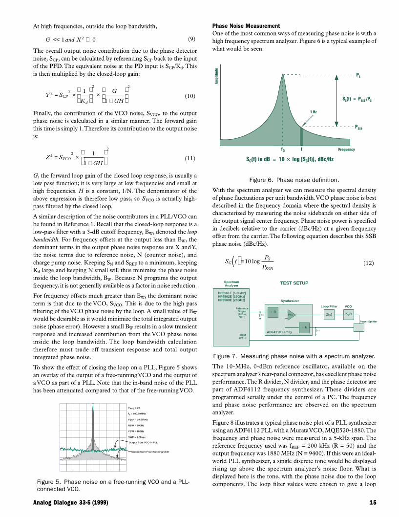
Figure 8 illustrates a typical phase noise plot of a PLL synthesizerusing an ADF4112 PLL with a Murata VCO, MQE520-1880. Thefrequency and phase noise were measured in a 5-kHz span. Thereference frequency used was fREF = 200 kHz (R = 50) and theoutput frequency was 1880 MHz (N = 9400). If this were an ideal-world PLL synthesizer, a single discrete tone would be displayedrising up above the spectrum analyzer’s noise floor. What isdisplayed here is the tone, with the phase noise due to the loopcomponents. The loop filter values were chosen to give a loop

16 Analog Dialogue 33-5 (1999)
bandwidth of approximately 20 kHz. The flat part of the phasenoise for frequency offsets less than the loop bandwidth is actuallythe phase noise as described by X2 and Y2 in the section “closingthe loop” for cases where f is inside the loop bandwidth. It isspecified at a 1-kHz offset. The value measured, the phase-noisepower in a 1-Hz bandwidth, was –85.86 dBc/Hz. It is made up ofthe following:
1. Relative power in dBc between the carrier and the sidebandnoise at 1-kHz offset.
2. The spectrum analyzer displays the power for a certainresolution bandwidth (RBW). In the plot, a 10-Hz RBW isused. To represent this power in a 1-Hz bandwidth, 10log(RBW)must be subtracted from the value obtained from (1).
3. A correction factor, which takes into account the implementa-tion of the RBW, the log display mode and detectorcharacteristic, must be added to the result obtained in (2).
4. Phase noise measurement with the HP 8561E can be madequickly by using the marker noise function, MKR NOISE. Thisfunction takes into account the above three factors and displaysthe phase noise in dBc/Hz.
The phase noise measurement above is the total output phase noiseat the VCO output. If we want to estimate the contribution of thePLL device (noise due to phase detector, R&N dividers and thephase detector gain constant), the result must be divided by N2
(or 20 × logN be subtracted from the above result). This gives aphase-noise floor of [–85.86 – 20 × log(9400)] = –165.3 dBc/Hz.
Reference SpursIn an integer-N PLL (where the output frequency is aninteger multiple of the reference input), reference spurs arecaused by the fact that the charge pump output is beingcontinuously updated at the reference frequency rate. Consider
again the basic model for the PLL which was discussed in Part 1of this series. This is shown again in Figure 9.
When the PLL is in lock, the phase and frequency inputs to thePFD (fREF and fN) are essentially equal, and, in theory, one wouldexpect that there to be no output from the PFD. However, thiscan create problems (to be discussed in Part 3 of this series), sothe PFD is designed such that, in the locked condition, the currentpulses from the charge pump will typically be as shown in Figure 10.
FREF
FN
IOUT
Figure 10. Output current pulses from the PFD chargepump.
Although these pulses have a very narrow width, the fact that theyexist means that the dc voltage driving the VCO is modulated by asignal of frequency fREF. This produces reference spurs in the RFoutput occurring at offset frequencies that are integer multiples offREF. A spectrum analyzer can be used to detect reference spurs.Simply increase the span to greater than twice the referencefrequency. A typical plot is shown in Figure 11. In this case thereference frequency is 200 kHz and the diagram clearly showsreference spurs at ±200 kHz from the RF output of 1880 MHz.The level of these spurs is –90 dB. If the span were increased tomore than four times the reference frequency, we would also seethe spurs at (2 × fREF).
VAVG = 100
Span = 500kHz
RBW = 3.0kHz
VBW = 3.0kHz
SWP = 140ms
MKR = -75dB, 200kHz
RL = 0dBm
10dB per division
+100KHz +200KHz-100KHz-200KHz 1880MHz
Figure 11. Output spectrum showing reference spurs.
Charge Pump Leakage CurrentWhen the CP output from the synthesizer is programmed to thehigh impedance state, there should, in theory, be no leakage currentflowing. In practice, in some applications the level of leakagecurrent will have an impact on overall system performance. Forexample, consider an application where a PLL is used in open-loop mode for frequency modulation—a simple and inexpensiveway of implementing FM that also allows higher data rates thanmodulating in closed-loop mode. For FM, a closed-loop methodworks fine but the data rate is limited by the loop bandwidth.
VAVG = 34
Span = 5.00kHz
RBW = 10Hz
VBW = 10Hz
SWP = 1.91sec
MKR = -79dB
MKR Noise = -85.86dBc/Hz
RL = 0dBm
+1KHz +2KHz-1KHz-2KHz 1880MHz
10dB per division
PHASE NOISE PLOT
Figure 8. Typical spectrum-analyzer output.
N1
FREF( UREF )
FO( UO )
+
-
e(s)PFD Kd Z(s) Kv
s
CP
Error Detector Loop Filter VCO
Feedback Divider
FN( UN )
Figure 9. Basic PLL model.

Analog Dialogue 33-5 (1999) 17
A system that uses open-loop modulation is the European cordlesstelephone system, DECT. The output carrier frequencies are in arange of 1.77 GHz to 1.90 GHz and the data rate is high;1.152 Mbps.
N1
XTAL FO
+
-PFD Kd Z(s) Kv
s
CP
Error Detector Loop Filter VCO
Feedback Divider
R1
GaussianFilter
Figure 12. Block diagram of open-loop modulation.
A block diagram of open-loop modulation is shown in Figure 12.The principle of operation is as follows: The loop is initially closedto lock the RF output, fOUT = N fREF. The modulating signal isturned on and at first the modulation signal is simply the dc meanof the modulation. The loop is then opened, by putting the CPoutput of the synthesizer into high-impedance mode, and themodulation data is fed to the Gaussian filter. The modulatingvoltage then appears at the VCO where it is multiplied by KV. Whenthe data burst finishes, the loop is returned to the closed loopmode of operation.
As the VCO usually has a high sensitivity (typical figures arebetween 20 and 80 MHz/volt), any small voltage drift before theVCO will cause the output carrier frequency to drift. This voltagedrift, and hence the system frequency drift, is directly dependenton the leakage current of the charge pump, CP, when in the highimpedance state. This leakage will cause the loop capacitor tocharge or discharge depending on the polarity of the leakagecurrent. For example, a leakage current of 1 nA would cause thevoltage on the loop capacitor (1000 pF for example) to charge ordischarge by dV/dt = I/C (1 V/s in this case). This, in turn, wouldcause the VCO to drift. So, if the loop is open for 1 ms and the KV
of the VCO is 50 MHz/Volt, the frequency drift caused by 1-nAleakage into a 1000-pF loop capacitor would be 50 kHz. In fact,the DECT bursts are generally shorter (0.5 ms), so the drift willbe even less in practice for the loop capacitance and leakage currentused in the example. However, it does serve to illustrate theimportance of charge-pump leakage in this type of application.
Receiver SensitivityReceiver sensitivity specifies the ability of the receiver to respond toa weak signal. Digital receivers use maximum bit-error rate (BER)at a certain rf level to specify performance. In general, device gains,noise figures, image noise, and local-oscillator (LO) wideband noiseall combine to produce an equivalent noise figure. This is thenused to calculate the overall receiver sensitivity.
Wideband noise in the LO can elevate the IF noise level and thusdegrade the overall noise factor. For example, wideband phasenoise at FLO + FIF will produce noise products at FIF. This directlyimpacts the receiver sensitivity. This wideband phase noise isprimarily dependent on the VCO phase noise.
Close-in phase noise in the LO will also impact sensitivity.Obviously, any noise close to FLO will produce noise products closeto FIF and impact sensitivity directly.
Receiver SelectivityReceiver selectivity specifies the tendency of a receiver to respondto channels adjacent to the desired reception channel. Adjacent-channel interference (ACI), a commonly used term in wirelesssystems, is also used to describe this phenomenon. Whenconsidering the LO section, the reference spurs are of particularimportance with regard to selectivity. Figure 13 is an attempt toillustrate how a spurious signal at the LO, having the same spacingas the channel-spacing frequency, can translate energy from anadjacent radio channel directly onto the IF. This is of particularconcern if the desired received signal is distant and weak and theunwanted adjacent channel is nearby and strong, which can oftenbe the case. So, the lower the reference spurs in the PLL, the betterit will be for system selectivity.
ConclusionIn Part 2 of this series we have discussed some of the criticalspecifications associated with PLL synthesizers, describedmeasurement techniques, and shown examples of results. Inaddition, there has been a brief discussion of the systemimplications of phase noise, reference spurs and leakage current.
In the final part of this series, we will examine the building blocksthat go to make up a PLL synthesizer. In addition, there will be acomparison between integer-N and fractional-N architectures forPLL.
AcknowledgmentThe authors would like to acknowledge Brendan Daly of the AnalogDevices GP RF Applications Group in Limerick for the plots of phasenoise and reference spurs.
References1. Mini-Circuits Corporation, VCO Designers’ Handbook, 1996.
2. L.W. Couch, Digital and Analog Communications Systems,Macmillan Publishing Company, New York, 1990.
3. P. Vizmuller, RF Design Guide, Artech House, 1995.
4. R.L. Best, Phase Locked Loops: Design, Simulation andApplications, 3rd edition, McGraw-Hill, 1997.
5. D.E. Fague, “Open Loop Modulation of VCOs for CordlessTelecommunications,” RF Design, July 1994.
6. D. B. Leeson, “A Simplified Model of Feedback Oscillator NoiseSpectrum,” Proceedings of the IEEE, Volume 42, February 1965,pp. 329–330. b
RFLO IFIF
IF Frequency
Ampl
itude
Figure 13. Adjacent Channel Interference.

18 Analog Dialogue 33-7 (1999)
Phase Locked Loopsfor High-FrequencyReceivers andTransmitters—Part 3Mike Curtin and Paul O’BrienThe first part of this series introduced phase-locked loops (PLLs),described basic architectures and principles of operation. It alsoincluded an example of where a PLL is used in communicationssystems. In the second part of the series, critical performancespecifications, like phase noise, reference spurs, and output leakage,were examined in detail, and their effects on system performancewere considered. In this, the last part of the series, we will dealwith some of the main building blocks that go to make up thePLL synthesizer. We will also compare integer-N and fractional-Narchitectures. The series will end with a summary of VCOs currentlyavailable on the market and a listing of the Analog Devices familyof synthesizers.
PLL Synthesizer Basic Building BlocksA PLL synthesizer can be considered in terms of several basicbuilding blocks. Already touched upon, they will now be dealt within greater detail:
Phase-Frequency Detector (PFD)Reference Counter (R)Feedback Counter (N)
The Phase-Frequency Detector (PFD)The heart of a synthesizer is the phase detector—or phase-frequency detector. This is where the reference frequency signal iscompared with the signal fed back from the VCO output, and theresulting error signal is used to drive the loop filter and VCO. In adigital PLL (DPLL) the phase detector or phase-frequency detectoris a logical element. The three most common implementations are :
Exclusive-or (EXOR) GateJ-K Flip-FlopDigital Phase-Frequency Detector
Here we will consider only the PFD, the element used in theADF4110 and ADF4210 synthesizer families, because—unlike theEXOR gate and the J-K flip flop—its output is a function of boththe frequency difference and the phase difference between the twoinputs when it is in the unlocked state.
Figure 1 shows one implementation of a PFD, basically consistingof two D-type flip flops. One Q output enables a positive currentsource; and the other Q output enables a negative current source.Assuming that, in this design, the D-type flip flop is positive-edgetriggered, the states are these (Q1, Q2):
11—both outputs high, is disabled by the AND gate (U3) backto the CLR pins on the flip flops.
00—both P1 and N1 are turned off and the output, OUT, isessentially in a high impedance state.
10—P1 is turned on, N1 is turned off, and the output is at V+.
01—P1 is turned off, N1 is turned on, and the output is at V–.
HI
HI
D1
D2
+IN
–IN
Q1
Q2
V+
V– (0V)
CLR1
CLR2
OUT
P1
N1
DELAY
U1
U2
U3
U4UP
DOWN
Figure 1. Typical PFD using D-type flip flops.
Consider now how the circuit behaves if the system is out of lockand the frequency at +IN is much higher than the frequency at–IN, as exemplified in Figure 2.
+IN
–IN
OUT
Figure 2. PFD waveforms, out of frequency and phase lock.
Since the frequency at +IN is much higher than that at –IN, theoutput spends most of its time in the high state. The first risingedge on +IN sends the output high and this is maintained untilthe first rising edge occurs on –IN. In a practical system this meansthat the output, and thus the input to the VCO, is driven higher,resulting in an increase in frequency at –IN. This is exactly whatis desired.
If the frequency on +IN were much lower than on –IN, the oppositeeffect would occur. The output at OUT would spend most of itstime in the low condition. This would have the effect of drivingthe VCO in the negative direction and again bring the frequencyat –IN much closer to that at +IN, to approach the lockedcondition. Figure 3 shows the waveforms when the inputs arefrequency-locked and close to phase-lock.
+IN
–IN
OUT
Figure 3. PFD waveforms, in frequency lock but out of phaselock.
Since +IN is leading –IN, the output is a series of positive currentpulses. These pulses will tend to drive the VCO so that the –INsignal become phase-aligned with that on +IN.
When this occurs, if there were no delay element between U3 andthe CLR inputs of U1 and U2, it would be possible for the outputto be in high-impedance mode, producing neither positive nor

Analog Dialogue 33-7 (1999) 19
negative current pulses. This would not be a good situation. TheVCO would drift until a significant phase error developed andstarted producing either positive or negative current pulses onceagain. Over a relatively long period of time, the effect of this cyclingwould be for the output of the charge pump to be modulated by asignal that is a subharmonic of the PFD input reference frequency.Since this could be a low frequency signal, it would not beattenuated by the loop filter and would result in very significantspurs in the VCO output spectrum, a phenomenon known as thebacklash effect. The delay element between the output of U3 andthe CLR inputs of U1 and U2 ensures that it does not happen.With the delay element, even when the +IN and –IN are perfectlyphase-aligned, there will still be a current pulse generated at thecharge pump output. The duration of this delay is equal to thedelay inserted at the output of U3 and is known as the anti-backlashpulse width.
The Reference CounterIn the classical Integer-N synthesizer, the resolution of the outputfrequency is determined by the reference frequency applied to thephase detector. So, for example, if 200-kHz spacing is required(as in GSM phones), then the reference frequency must be200 kHz. However, getting a stable 200-kHz frequency source isnot easy. A sensible approach is to take a good crystal-based highfrequency source and divide it down. For example, the desiredfrequency spacing could be achieved by starting with a 10-MHzfrequency reference and dividing it down by 50. This approach isshown in the diagram in Figure 4.
FREF
PHASEDETECTOR
LOWPASS
FILTERVCO FOUT = FREF 3 N/R
FOUT = F1 3 NFOUT = (FREF/R) 3 NFOUT = (FREF) 3 (N/R)÷ N
COUNTER
REFERENCEDIVIDER
÷ R
F1
Figure 4. Using a reference counter in a PLL synthesizer.
The Feedback Counter, NThe N counter, also known as the N divider, is the programmableelement that sets the relationship between the input and outputfrequencies in the PLL. The complexity of the N counter has grownover the years. In addition to a straightforward N counter, it hasevolved to include a prescaler, which can have a dual modulus.
This structure has grown as a solution to the problems inherent inusing the basic divide-by-N structure to feed back to the phasedetector when very high-frequency outputs are required. Forexample, let’s assume that a 900-MHz output is required with 10-kHz spacing. A 10-MHz reference frequency might be used, withthe R-Divider set at 1000. Then, the N-value in the feedback wouldneed to be of the order of 90,000. This would mean at least a 17-bit counter capable of dealing with an input frequency of 900 MHz.
To handle this range, it makes sense to precede the programmablecounter with a fixed counter element to bring the very high inputfrequency down to a range at which standard CMOS will operate.This counter, called a prescaler, is shown in Figure 5.
However, using a standard prescaler introduces other complica-tions. The system resolution is now degraded (F1 × P). This issuecan be addressed by using a dual-modulus prescaler (Figure 6). Ithas the advantages of the standard prescaler but without any lossin system resolution. A dual-modulus prescaler is a counter whose
FREF
PHASEDETECTOR
LOWPASS
FILTERVCO FOUT = FREF 3 NP/R
FOUT = F1 3 N 3 PFOUT = (FREF/R) 3 N 3 PFOUT = (FREF) 3 (NP/R)PRESCALER
÷ P
REFERENCEDIVIDER
÷ R
F1
÷ NCOUNTER
Figure 5. Basic prescaler.
division ratio can be switched from one value to another by anexternal control signal. By using the dual-modulus prescaler withan A and B counter one can still maintain output resolution of F1.However, the following conditions must be met:
÷ BCOUNTER
DUAL MODULUSPRESCALER
÷ P/P + 1
÷ ACOUNTER CONTROL:
LOW P,HIGH (P + 1)
LOAD
LOAD
TOTAL NUMBER OF COUNTS OF F OUT IN A FULL F 1 CYCLEA 3 (P + 1) + (B – A)PAP + A +BP – APBP + AFOUT = F1 3 (BP + A)FOUT = (FREF/R) 3 (BP + A)
FREF
PHASEDETECTOR
LOWPASS
FILTERVCO FOUT
REFERENCEDIVIDER
÷ R
F1
Figure 6. Dual-modulus prescaler.
1. The output signals of both counters are High if the countershave not timed out.
2. When the B counter times out, its output goes Low, and itimmediately loads both counters to their preset values.
3. The value loaded to the B counter must always be greater thanthat loaded to the A counter.
Assume that the B counter has just timed out and both countershave been reloaded with the values A and B. Let’s find the numberof VCO cycles necessary to get to the same state again.
As long as the A counter has not timed out, the prescaler is dividingdown by P + 1. So, both the A and B counters will count down by1 every time the prescaler counts (P + 1) VCO cycles. This meansthe A counter will time out after ((P + 1) × A) VCO cycles. At thispoint the prescaler is switched to divide-by-P. It is also possible tosay that at this time the B counter still has (B – A) cycles to gobefore it times out. How long will it take to do this: ((B – A) × P).The system is now back to the initial condition where we started.
The total number of VCO cycles needed for this to happen is :
N = (A × (P + 1)) + ((B – A) × P)
= AP + A + BP – AP
= A + BP
When using a dual-modulus prescaler, it is important to considerthe lowest and highest values of N. What we really want here is therange over which it is possible to change N in discrete integersteps. Consider the expression N = A + BP. To ensure a continuousinteger spacing for N, A must be in the range 0 to (P – 1). Then,every time B is incremented there is enough resolution to fill in allthe integer values between BP and (B + 1)P. As was already notedfor the dual-modulus prescaler, B must be greater than or equalto A for the dual modulus prescaler to work. From these we can

20 Analog Dialogue 33-7 (1999)
say that the smallest division ratio possible while being able toincrement in discrete integer steps is:
NMIN = (Bmin × P) + Amin
= ((P – 1) × P) + 0
= P2 – PThe highest value of N is given by
NMAX = (Bmax × P) + Amax
In this case Amax and Bmax are simply determined by the size of theA and B counters.
Now for a practical example with the ADF4111.Let’s assume that the prescaler is programmed to 32/33.A counter: 6 bits means A can be 26 – 1 = 63B counter: 13 bits means B can be 213 – 1 = 8191
NMIN = P2 – P = 992
NMAX = (Bmax × P) + Amax
= (8191 × 32) + 63
= 262175
ADF4110 FamilyThe building blocks discussed in the previous sections are all usedin the new families of integer-N synthesizers from ADI. TheADF4110 family of synthesizers consists of single devices and the
ADF4210 family consists of dual versions. The block diagram forthe ADF4110 is shown below. It contains the reference counter,the dual-modulus prescaler, the N counter and the PFD blocksdescribed above.
Fractional-N Synthesizers*Many of the emerging wireless communication systems have aneed for faster switching and lower phase noise in the local oscillator(LO). Integer N synthesizers require a reference frequency thatis equal to the channel spacing. This can be quite low and thusnecessitates a high N. This high N produces a phase noise thatis proportionally high. The low reference frequency limits thePLL lock time. Fractional-N synthesis is a means of achievingboth low phase noise and fast lock time in PLLs.
The technique was originally developed in the early 1970s. Thisearly work was done mainly by Hewlett Packard and Racal. Thetechnique originally went by the name of “digiphase” but it laterbecame popularly named fractional-N.
In the standard synthesizer, it is possible to divide the RF signalby an integer only. This necessitates the use of a relatively lowreference frequency (determined by the system channel spacing)and results in a high value of N in the feedback. Both of thesefacts have a major influence on the system settling time and thesystem phase noise. The low reference frequency means a longsettling time, and the high value of N means larger phase noise.
REFIN14-BIT
R COUNTER
CLKDATA
LE
CHARGEPUMP
MUXMUXOUT
ADF4110ADF4111ADF4112
RFINA
CP
AVDD DVDD VP
CE AGND DGND
CPGND
RFINB
RSET
R COUNTERLATCH
22
14
REFERENCE
LOCKDETECT
CPI3 CPI2 CPI1
M3 M2 M1LOAD
LOAD
19
13
6
CURRENTSETTING 2
CPI6 CPI5 CPI4
SDOUT
SDOUT
VCC1
High Z
N = BP + A
FROMFUNCTION
LATCH
FUNCTIONLATCH
A, BCOUNTER
LATCH
PHASE/FREQUENCYDETECTOR
CURRENTSETTING 124-BIT
INPUT REGISTER
13-BITB COUNTER
6-BITA COUNTER
PRESCALERP/P+1
+
–
Figure 7. Block diagram for the ADF4110 family.
*The authors are indebted to The McGraw-Hill Companies for permission touse copyrighted material from Reference 4 in this section.

Analog Dialogue 33-7 (1999) 21
If division by a fraction could occur in the feedback, it would bepossible to use a higher reference frequency and still achieve thechannel spacing. This lower fractional number would also meanlower phase noise.
In fact it is possible to implement division by a fraction over along period of time by alternately dividing by two integers (divideby 2.5 can be achieved by dividing successively by 2 and 3).
So, how does one divide by X or (X + 1) (assuming that thefractional number is between these two values)? Well, the fractionalpart of the number can be allowed to accumulate at the referencefrequency rate.
OVERFLOW
S
DAC
θε
FREFLOWPASS
FILTERVCO FOUT
PULSEREMOVING
CIRCUIT
PHASEDETECTOR
÷ NCOUNTER
FYFX
N REGISTER F REGISTER ACCUMULATOR
REMOVE COMMAND
+
+
Figure 8. Fractional-N synthesizer.
Then every time the accumulator overflows, this signal can be usedto change the N divide ratio. This is done in Figure 8 by removingone pulse being fed to the N counter. This effectively increases thedivide ratio by one every time the accumulator overflows. Also,the bigger the number in the F register, the more often theaccumulator overflows and the more often division by the largernumber occurs. This is exactly what is desired from the circuit.There are some added complications however. The signal beingfed to the phase detector from the divide-by-N circuit is notuniform in real time. Instead it is being modulated at a ratedetermined by the reference frequency and the programmedfraction. This is turn modulates the phase detector output andgoes to the VCO input. The end result is a high spurious contentat the output of the VCO. Major efforts are currently under way tominimize these spurs. One method uses the DAC shown in Figure 8.
Up to now, monolithic Fractional-N synthesizers have failed tolive up to expectations but the eventual benefits that may be realizedmean that development is continuing at a rapid pace.
Summary of VCO ManufacturersWith the explosive growth in wireless communications, the demandfor products like synthesizers and VCOs has increased dramaticallyover the past five years. Interestingly, until now, the markets havebeen served by two distinct sets of manufacturers. Below is listed
a selection of players in the VCO field. This list is not meant to beall-inclusive, but rather gives the reader a feel for some of themain players.
VCOsMurata Murata has both 3-V and 5-V devices available.
The VCOs are mainly narrowband for wirelesshandsets and base stations. Frequencies aredetermined by the wireless frequency standards.
Vari-L Vari-L addresses the same market as Murata. 3-Vand 5-V devices are available.
Alps Alps makes VCOs for wireless handsets and basestations.
Mini-Circuits Mini-Circuits offers both narrowband and wide-band VCOs.
Z-Comm Z-Communications has both wideband andnarrowband VCOs. The wideband VCOs typicallyhave an octave tuning range (1 GHz to 2 GHz, forexample) and operate from a supply voltage of upto 20 V. They offer surface-mount packaging.
Micronetics Micronetics offers both narrowband and widebandVCOs. Their strength lies more in the widebandproducts where they can go from an octave rangeat anything up to 1200 MHz. Above these outputfrequencies, the range is somewhat reduced.
The Analog Devices Synthesizer FamilyThe table on the next page lists current and future members ofthe ADF4xxx synthesizer family. It includes single and dual, andinteger-N and fractional-N devices.
AcknowledgementsThe ADF4xxx Family of synthesizers is designed at the AnalogDevices facility in Limerick, Ireland. The product line teamincludes: Mike Tuthill, Leo McHugh, Bill Hunt, Mike Keaveney,Brendan Daly, Paul O’Brien, Paul Mallon, Ian Collins, SineadO’Keefe, Liam McCann, Patrick Walsh, Cristoir O’Reilly, PaulLaven, Samuel Landete, Niall Kearney, and Mike Curtin. Thegroup would like to acknowledge the valuable contributions ofJon Strange and Ashish Shah at Analog Devices, Kent (U.K.), andof Fred Weiss at Analog Devices Northwest Labs (Beaverton, OR).
References1. Mini-Circuits Corporation, VCO Designer’s Handbook, 1996.
2. L.W. Couch, Digital and Analog Communications Systems,Macmillan Publishing Company, New York, 1990.
3. P. Vizmuller, RF Design Guide, Artech House, 1995.
4. R.L. Best, Phase Locked Loops: Design, Simulation andApplications, 3rd Edition, McGraw-Hill, 1997. b

22 Analog Dialogue 33-7 (1999)
Integer-N Fractional-N Single/ Pin SecondDevice Frequency Range Frequency Range Dual Count Source
ADF4110 ≤550 MHz Single 16ADF4111 ≤1.2 GHz Single 16ADF4112 ≤3.0 GHz Single 16ADF4113 ≤3.8 GHz Single 16
ADF4116 ≤550 MHz Single 16 LMX2306ADF4117 ≤1.2 GHz Single 16 LMX2316ADF4118 ≤3.0 GHz Single 16 LMX2326
ADF4210 ≤510 MHz/≤1.2 GHz Dual 20ADF4211 ≤510 MHz/≤2.0 GHz Dual 20ADF4212 ≤510 MHz/≤3.0 GHz Dual 20ADF4213 ≤1.0 GHz/≤2.5 GHz Dual 20
ADF4216 ≤510 MHz/≤1.2 GHz Dual 20 LMX2332LADF4217 ≤510 MHz/≤2.0 GHz Dual 20 LMX2331LADF4218 ≤510 MHz/≤2.5 GHz Dual 20 LMX2330L
ADF4206 ≤500 MHz/≤500 MHz Dual 16 LMX2337ADF4207 ≤1.1 GHz/≤1.1 GHz Dual 16 LMX2335ADF4208 ≤1.1 GHz/≤2.0 GHz Dual 20 LMX2336
ADF4150 ≤550 MHz Single 16ADF4151 ≤1.2 GHz Single 16ADF4152 ≤3.0 GHz Single 16
ADF4156 ≤550 MHz Single 20ADF4157 ≤1.2 GHz Single 20ADF4158 ≤3.0 GHz Single 20
ADF4250 ≤550 MHz ≤1.2 GHz Dual 20ADF4251 ≤550 MHz ≤2.0 GHz Dual 20ADF4252 ≤1.0 GHz ≤3.0 GHz Dual 20
ADF4256 ≤550 MHz/≤1.2 GHz Dual 20ADF4257 ≤550 MHz/≤2.0 GHz Dual 20ADF4258 ≤1.0 GHz/≤3.0 GHz Dual 20
All brand or product names mentioned are trademarks or registered trademarks of their respective holders.
ADF4xxx Frequency Synthesizer Family
Codecs DSPMixed-Signal
Audio InterfaceProcessing
Sigma-DeltaConvertersHigh-SpeedConverters
OthelloRadio
Baseband RF
Power/Battery ManagementWireless
Transceivers

Analog Dialogue 33-1 (1999) 23
Dual Axis, Low g,Fully IntegratedAccelerometersBy Harvey WeinbergThe ADXL202 is the newest low-g (±2 g), dual-axis, surface-micromachined accelerometer from Analog Devices. Building onexperience gained in manufacturing millions of i MEMS®
accelerometers in the past six years, the ADXL202 is the world’sfirst commercial dual axis, surface micromachined accelerometerto combine low-g sensing with lowest power, lowest noise, anddigital outputs—all on a single silicon chip.
Surface micromachining, first commercialized with theADXL50, allows for integration of the acceleration sensor withall signal conditioning electronics—tight integration of the sensorand its signal conditioning is what has made this impressiveperformance possible.
Lower cost was a major driver in the ADXL202 design effort.Integrating two axes resulted in a significant cost reduction peraxis. In addition, while the ADXL50, ADXL150, and ADXL250can be thought of as “acceleration to volts” transducers, theADXL202 adds a Pulse Width Modulated (PWM) digital outputcapability as well. Since most accelerometers will interface with amicrocontroller, a PWM output obviates the need for an A to Dconverter, further driving down the user’s total system cost.
Sensor StructureAs with all of our accelerometer products, the sensor element is adifferential capacitor whose output is proportional to acceleration(basic sensor information can be seen in Analog Dialogue 27-2,1993, and Analog Dialogue 30-4, 1996). Since device performanceis so dependent on sensor design, a brief explanation of some ofthe key factors in beam design is appropriate.
The beam is made up of many interdigitated fingers. Each set offingers can be visualized as shown in Figure 1. The differentialcapacitance of each finger is proportional to the overlapping areabetween the fixed outer plates and the moving finger, and thedisplacement of the moving finger. Clearly these are very smallcapacitors, and in order to reduce noise and increase resolutionwe need as large a differential capacitance as practical.
Figure 1. Beam Dimensions for a Single Finger.
The capacitor area is limited by the 2-micron height—fixed byprocess technology, while the (125-micron) overlap is adjustableto some extent. However longer fingers are not desirable for severalreasons. Longer fingers are harder to manufacture and increasedbeam size translates to more expensive parts.
The movement of the beam is controlled by the polysilicon springsholding the beam. These springs and the beam’s mass obey thesame laws of physics we learned in high school. The force (F) on amass (m) subject to acceleration (a), according to Newton’s SecondLaw, is F = m a, and the deflection (x) of a restraining spring(obeying Hooke’s Law) is proportional to the applied force, F = k x,
and:
x = (m/k) a
The only two parameters under our control are the spring stiffness,or spring constant, (k), and mass (m). Reducing the spring constantseems like an easy way to improve beam sensitivity. But as usual,nothing comes for free. The resonant frequency of the beam isproportional to the spring constant, and the accelerometer mustoperate at frequencies below the resonant frequency. In addition,higher spring constants make for more rugged beams (higher shocksurvivability). So if we would like to keep the spring constant ashigh as possible the only parameter left to change is mass.
Adding mass normally implies a larger sensor area, resulting inmore expensive parts, since the only way to add mass it to makethe beam larger. In the ADXL202 a novel beam structure wasinvented, as shown in Figure 2. Rather than using two discretebeams placed orthogonally as in the ADXL250 (Analog Dialogue30-4, 1996, page 5, Figure 5), the fingers that constitute the Xand Y axis variable capacitors are integrated along the sides of asingle square beam. This results in a reduction of the overall sensorarea, yet the larger common beam mass enhances the resolutionof the ADXL202. A spring suspension system, shown in Figure 3,situated in the corners of the beam, was designed to minimizecross-axis sensitivity (i.e., with acceleration along one axis, anytendency toward motion or outputs in the orthogonal directionis suppressed).
Figure 2. ADXL202 Beam Structure.

24 Analog Dialogue 33-1 (1999)
Figure 3. Detail of One Corner of the ADXL202 Beam show-ing springs.
Circuit ArchitectureThe circuit architecture (shown in Figure 4) of the ADXL202 issimilar to the ADXL250 up to the demodulator. The fixed outerplates are driven with square waves that are 180 degrees out ofphase. When the movable fingers (and hence the beam) are centeredbetween the fixed outer plates, both sides of the differentialcapacitor have equal capacitance and the ac voltage on the beamis zero. However, if the beam is displaced due to an appliedacceleration, the differential capacitance will be unbalanced andan ac voltage of amplitude proportional to the displacement ofthe beam will result.
DEMOD
RFILT32kV
RFILT32kV
OSCILLATOR
X SENSOR
Y SENSOR
ADXL202
X OUT
Y OUT
SELF TESTXFILTVDDVDD
CX
+3.0V TO +5.25V
CDC
COM YFILT T2
CYRSET
COUNTER
mP
T2
T1
A(g) = (T1/T2 – 0.5)/12.5%0g = 50% DUTY CYCLET2 = RSET/125MV
DEMOD
DUTYCYCLE
MODULATOR(DCM)
Figure 4. ADXL202 Circuit Architecture.
© Analog Devices, Inc., 1995–1999All brand or product names mentioned are trademarks or registered trademarks of their respective holders.iMEMS is a registered trademark of Analog Devices, Inc.: integrated MicroElectronic Machines.
This ac voltage is amplified and then demodulated by asynchronous demodulator. The output of the demodulator drivesthe duty cycle modulator through a 32-kΩ resistor. Here a pin isavailable on each channel to allow the user to set the bandwidthby adding two external capacitors (one per channel) creating asimple first-order RC low pass filter. The low pass filtered signalis converted to a PWM signal by the duty cycle modulator. Theperiod of the PWM output may be set from 0.5 to 10 ms, using asingle resistor.
Performance and ApplicationsJust as it was impossible 25 years ago to predict where low-costlasers would turn up, today it’s difficult to imagine the large numberof applications where low-cost accelerometers will be used. TheADXL202 breaks so many performance-vs.-cost barriers that mostof its really successful applications are not classically“accelerometer” (literally “acceleration-measuring”) applications.They are now being used in car alarms, machine health monitoring,joysticks, game pads, and other computer input devices.
As mentioned in the introduction, the ADXL202 is the lowestnoise dual axis surface micromachined accelerometer in productiontoday. With its typical noise density of 500 mg/√Hz, it is possibleto resolve inclinations of better than ±1° of tilt at bandwidths ofup to 50 Hz. The high-resolution (approximately 14-bit) duty-cycle modulator allows users to take advantage of the ADXL202’scapabilities in low cost systems. These capabilities have openedthe door to several other non-traditional applications, such as caralarms (where they are used to sense jacking-up or towing) andautomatic machine leveling.
Support ToolsExtensive support tools are available for designers. The hardwaretools available are a simple evaluation PCB with an ADXL202 inits minimum circuit configuration (part number ADXL202EB),and the ADXL202EB-232, a complete 2-axis data acquisitionsystem that interfaces to a PC. Primarily targeted at designers whoneed to fully understand how acceleration measurement will enabletheir application or product, the ADXL202EB-232 includessoftware for viewing accelerometer signals and data logging.
The ADXL202 Interactive Designer is an Excel-based spreadsheetmodel that takes the user through the design process of selectingADXL202 components and defining software parameters formicrocontroller interface. The spreadsheet outputs componentvalues and information about the resolution, bandwidth andacquisition rate of your design. It is available free at the Web sitelisted below.
Also available at that site are several hardware and softwarereference designs, highlighting different interface techniquesand a variety of application notes. Each reference designincludes flow charts and source code for various popularmicrocontrollers, as well as a description of where each dataacquisition method is appropriate. These documents can befound at http://www.analog.com/iMEMS/products/ADXL202_top.html. b

Analog Dialogue 33-8 (1999) 25
Ask the Applications Engineer—29By Harvey Weinberg
ACCELEROMETERS—FANTASY & REALITY
Q. As an Applications Engineer for the Micromachined ProductsDivision supporting the compact, low-cost, gravity-sensitive AnalogDevices line of integrated accelerometers1 you must get to hear lotsof creative ideas from prospective customers about how to employaccelerometers in useful ways.
A. Yes, but sometimes what they are suggesting violates physicallaws! We’ve come to rate them in various categories on aninformal “reality” scale:
• Real – A real application that actually works today and iscurrently in production.
• Possible – An application that is technically feasible, butnot (to our knowledge) in production.
• Fantasy – An application that could be possible if we hadmuch better technology.
• Dream Land – An application that would be nice, but anypractical implementation we can think of would violate somephysical laws.
Would you like to see some of these ideas (the ones we’re freeto mention), hear about their potential benefits, think aboutthem, and guess which category they belong in?
Q. Sure, go ahead.
A. O.K. You can find (and link to) the answers, with commentary,below.
Washing Machine Load BalancingUnbalanced loads during the high-speed spin-cycle causewashing machines to shake, and in some cases, to even “walk”across the floor if unrestrained. An accelerometer senses theaccelerations present during the unbalanced spin. If such animbalance is present, the washing machine redistributes theload by jogging the drum back and forth a few times until theload is balanced. Real or fantasy? See answer A.
Machine Health MonitorsMany industries change or overhaul mechanical equipmentusing a calendar-based preventive maintenance schedule. Thisis especially true in applications where one cannot afford ortolerate unscheduled down-time. So machinery with plenty ofservice life left is often prematurely rebuilt at a cost of millionsof dollars across many industries. By embedding accelerometersin bearings, or other rotating equipment, service life can beextended without additional risk of sudden failure.
The accelerometer senses the vibration of bearings or otherrotating equipment to determine their condition. Realor fantasy? See answer B.
Automatic LevelingAccelerometers measure the absolute inclination of an object(e.g. a large machine, a mobile home, etc.). The tilt informationis used by a microcontroller to automatically level it. Real orfantasy? See answer C.
Scroll Control for PDAs and HandyphonesThe accelerometer allows the microcontroller to recognizegestures allowing the user one handed control of mobile devices.Real or fantasy? See answer D.
Car AlarmHere the accelerometer senses if a car is being jacked up orbeing picked up by a tow truck, and sets off the alarm. Real orfantasy? See answer E.
Ski BindingsThe accelerometer measures the total shock energy andsignature to determine if the binding should release. Real orfantasy? See answer F.
Personal NavigationIn this application, position is determined by dead reckoning(double integration of acceleration over time to determineactual position). Real or fantasy? See answer G.
Subwoofer Servo ControlAn accelerometer is mounted on the cone of the subwoofer toprovide positional feedback used to servo out distortion. Realor fantasy? See answer H.
Neuromuscular StimulatorThis application helps people, who have lost control of theirlower leg muscles, to walk—by stimulating muscles at theappropriate time. Real or fantasy? See answer I.
Car-Noise CancellationThe accelerometer senses low-frequency vibration in thepassenger compartment, and the noise-cancellation systemnulls it out, using the speakers in the car stereo system. Real orfantasy? See answer J.
ANSWERSA. Washing-machine load balancing: Real. This application iscurrently in production. With better load balance, faster spinrates can be used to wring more water out of clothing, makingthe drying process more efficient. Fewer mechanicalcomponents are required for damping the drum motion,making the overall system lighter, and less expensive. Inaddition, transmission and bearing service life may be extendedbecause of lower peak loads present on the motor. See http://www.analog.com/industry/ iMEMS/markets/industrial/washing_machine.html for more information about washingmachines. Go to next question.
B. Machine health monitoring: Possible. This application hasbeen demonstrated but is not yet in production.
Using the vibrational “signature” of bearings to determine theircondition is a well proven and industry-accepted method ofequipment maintenance, However, the cost of accelerometersand the associated signal conditioning equipment hasbeen traditionally too high. The ADXL1052 offers a completevibration measurement and signal conditioning solution on achip at very low cost. See http://www.analog.com/industry/iMEMS/markets/industrial/machine.html for more informationabout machine health. Go to next question.
1http://www.analog.com/industry/iMEMS.2http://products.analog.com/products/info.asp?product=ADXL105.
26 Analog Dialogue 33-8 (1999)
C. Automatic leveling: Real to Fantasy (depending on theapplication). There are some applications where this is practicaland currently in production. Others are too demanding forcurrent products.
Self-leveling is a very demanding application, as absoluteprecision is required. Surface micromachined accelerometershave impressive resolution, but absolute tilt measurement withhigh accuracy (to better than 1%) requires temperature stabilityand hysteresis performance that today’s surface-micromachinedaccelerometers cannot achieve. Applications needing absoluteaccuracy to within ±3° or more are currently possible and afew such applications are in production. Go to next question.
D. Scroll control: Real. This application is currently (or almost,depending on press time) in production.
A PDA (like the 3com Palm Pilot) is incredibly handy, butalmost impossible to use one-handed. Like when you’re driving,or on the phone. Adding an accelerometer lets the PDA acceptgesture inputs, like tilting up or down, to control the cursor orpage up/down control. See http://www.analog.com/industry/iMEMS/markets/consumer/peripherals.html if you areinterested in game controllers or are a Palm Pilot user andwant to see how to add a tilt function to your PDA. Go tonext question.
E. Car alarm: Real. This application is currently in productionin OEM and after-market automotive anti-theft systems.
One of the most popular methods of auto theft is where thecar is stolen by simply towing it away. Conventional car alarmsdo not protect against this. Shock sensors cannot measurechanges in inclination, and ignition-disabling systems areineffectual. Here is an application where the high-resolutioncapabilities of the ADXL202 are used to advantage. Theaccelerometer measures if the car’s inclination is changing bymore than 0.5° per minute. If so, the alarm is sounded,hopefully scaring off the would-be thief. Absolute stability isnot required here (unlike automatic leveling systems) astemperature does not change significantly in a minute or less.See http://www.analog.com/industry/ iMEMS/markets/automotive/car_alarms.html if you’re interested in car alarms.Go to next question.
F. Ski bindings: Fantasy. This is a practical accelerometerapplication, but current battery technology (particularly lowtemperature performance) makes it impractical.
All mechanical ski bindings are highly evolved, but limited intheir performance. Measuring the actual shock experiencedby the skier would be a much more accurate way to determineif a binding should release. Intelligent systems could bedeveloped that could take each individual’s capability andphysiology into account. Smaller and lighter batteries thatperform well at low temperatures will, eventually, enable thisapplication. Go to next question.
G. Personal navigation: Dream Land. Long term integrationresults in the accumulation of error due to small dc errors inthe accelerometer, integrator input circuitry, wir ingthermocouples, etc. Double integration compounds the errors(t2). Without some way of “resetting” the actual position fromtime to time, huge errors result. This is analogous to building
an op-amp integrator by simply putting a capacitor across it.Even if the accelerometer’s accuracy is improved by ten or onehundred times better than currently available, huge errorswould still eventually result. It would just take longer to happen.
Accelerometers can be used in conjunction with a GPS systemwhen the GPS signals are briefly unavailable. Integration over ashort time (a minute or so) can give satisfactory results. See http://www.analog.com/industry/iMEMS/markets/consumer/car_nav.htmlfor more information about navigation. Go to next question.
H. Subwoofer servo: Real. Several active subwoofers with servocontrol are on the market today.
Servo control of subwoofers has several advantages. Harmonicdistortion, as well as power compression, can be greatlyreduced. In addition servo control can also electronically lowerthe Q of the speaker/enclosure system, enabling the use of smallerenclosures3. The ADXL1904 is small and light; its mass, addedto that of the loudspeaker cone, does not change the overallacoustic characteristics significantly. See http://www.analog.com/industry/iMEMS/markets/consumer/subwoofers.html for moreinformation about active subwoofer applications, and http://www.analog.com/industry/ iMEMS/markets/consumer/subwoofers/Subwoof.html#cir for circuits. Go to next question.
I. Neuromuscular stimulator: Real. This application is very near(if not already in) production.
When walking, the forefoot is normally raised when movingthe leg forward, then lowered when pushing the leg backward.The accelerometer is worn somewhere on the lower leg or foot,where it senses the position of the leg. The appropriate musclesare then electronically stimulated to flex the foot as required.
This is a classic example of how micromachined accelerometershave made a product feasible. Earlier models used a liquid tiltsensor or a moving ball bearing (acting as a switch) to determinethe leg position. Liquid tilt sensors had problems because ofsloshing of the liquid, so only slow walking was possible. Ball-bearing switches were easily confused when walking on hills.Using an accelerometer, the differential between leg back and legforward is measured, so hills do not fool the system and there areno liquid slosh problems. The low power consumption of theaccelerometer allows the system to work with a small lithiumbattery, making the overall package unobtrusive. Go to next question.
J. Car-noise cancellation: Dream Land. While the accelerometerhas no trouble picking up the vibration in the passengercompartment, noise cancellation is highly phase-dependent.So while we may cancel the noise in one location (say aroundthe head of the driver), it will probably be increased atother locations.
ConclusionBecause of their sensitivity, compactness, low cost, ruggedness,and ability to measure both static and dynamic accelerationforces, surface micromachined accelerometers have madenumerous new applications possible. Many of them were notanticipated because they were not thought of as classicaccelerometer applications. The imagination of designers nowseems to be the limiting factor in the scope of potentialapplications—but sometimes designers can become tooimaginative! While performance improvements continue toenable more applications, it’s wise to try to stay away from“solutions” that violate laws of physics. b
3See R. A. Greiner and T. M. Sims, Jr., Loudspeaker Distortion Reduction,Journal of the Audio Engineering Society, Vol. 32, No. 12.
4http://products.analog.com/products/info.asp?product=ADXL190.

Analog Dialogue 33-6 (1999) 27
ADXL105: A LowerNoise, Wider BandwidthAccelerometer RivalsPerformance of MoreExpensive Sensorsby James Doscher, Marketing Manager,Micromachined Product Division
INTRODUCTIONSurface micromachining has been used to make reliableaccelerometers in large quantities at very low cost, but with modestperformance, for the airbag and consumer products industry(Analog Dialogue 27-2 (1993), A-D 30-4 (1996), A-D 33-1 (1999)).The accuracy and noise limitations for more-sophisticatedapplications are due to the tiny signals involved, given the smallsize of surface-micromachined structures.
However, recent advances in circuit architectures and beamstructures used in integrated micro-electromechanical systems haveresulted in order-of-magnitude improvements in resolution andaccuracy. The recently introduced ADXL105 accelerometer has a225-µg/√Hz noise floor, 10-kHz bandwidth, and an on-boardtemperature sensor, which can be used for calibrating againsttemperature effects. In comparison, the ADXL50, the first AnalogDevices accelerometer, had a noise floor of 6500 µg/√Hz . A 65-µg/√Hz version has also been demonstrated on ADI’s new 3-µmpolysilicon process. The ADXL105 is initially targeted at machinehealth and tactical guidance & control applications, as well as anumber of new automotive applications.
The ADXL105, a near ideal kind of vibration sensor, eliminatessignificant problems with existing vibration sensors, such aspiezoelectric and bulk capacitive sensors. Primary benefits derivefrom much lower cost, stable sensitivity as a function of frequencyand temperature, ruggedness, and ease of use. Besides machinehealth and condition monitoring, it is particularly well suited fornoise and vibration cancellation applications.
Structurally, the ADXL105 is the first of a new generation ofprecision surface-micromachined devices that attempts to pushthe performance envelope using a 2-µm-thick polysilicon process.The device is fabricated on a process that combines the surface-micromachined differential-capacitance sensor and the electronicsignal conditioning circuitry on a single IC chip. The sensor itselfis 0.5 mm × 0.4 mm and 2-µm-thick, with 1-µm feature size and amass of only 0.5 micrograms. The deflection due to a 1-gacceleration is 1 nanometer (E-9 m), or about 0.07% of the gapwidth, and the minimum resolvable deflection is about210 femtometers (E-15 m), or 0.002 Angstrom units, at a noiselevel of 225 µg/√Hz and 1-Hz bandwidth.
With a source capacitance in the neighborhood of 150 femtofarads(i.e., 0.15 pF), and orders-of-magnitude smaller differentialcapacitance changes (100 attofarads (E-18 F) for a 1-g accelerationand 23 zeptofarads (E-21 F) resolution, the signal output of these
devices could be easily lost in the presence of parasitic capacitanceor noise.
The ability to provide on-chip signal conditioning is what allowsthe minute signals to be read with minimal interference. Asynchronous demodulation technique (“ac bridge”) is used toincrease noise immunity and improve signal to noise. A square-wave carrier drives the sensor, and the modulated signal producedby the change in differential capacitance is amplified andsynchronously demodulated, minimizing noise and boosting thesignal-to-noise ratio.
The limitations on size and mass of the structural beam place aweighty constraint on the performance of these devices. To makea precision accelerometer, it is helpful to have as much mass aspossible and a large output signal from the sensor. But bothparameters are limited by the size of the sensor element, which inturn is limited by the ability to control the curvature, or out-of-plane deviation of the structure due to internal polysilicon stress.Limits on size (hence mass) set a lower noise limit on the sensor,because the Brownian noise floor of the device, which is imposedby gas molecules bouncing off the beam, is inversely proportionalto the mass of the sensor. Signal to noise is of course limited bythe size of the signal, (related to spring stiffness, mass of the sensor,and source capacitance), as well as the noise floor set by the front-end circuitry.
Spring stiffness limits capacitance change, hence the magnitudeof the electrical output. Although more-flexible springs allowgreater travel of the mass under acceleration, with a correspondingincrease in the delta capacitance read by the circuit, there is adirect trade-off between the flexibility of the springs and therobustness of the structure to shock and overload. If sensors areinsufficiently stiff, their elements can touch, and the resultingstiction (static friction) produces a failure through irreversiblephysical latchup.
The design goal of the ADXL105 was to improve the robustnessof the sensor, and at the same time achieve an approximately 5×improvement in performance over existing products built in theprocess; this would improve the suitability of the devices formachine health and tactical inertial applications.
VDD
TOUT
ST
COM AOUT VMID VINVNIN UCAOUT
UNCOMMITTEDAMPLIFIER
ADXL105
X SENSOR
TEMPSENSOR
OUTPUT
VDD
R1 R2
+V
COM
0.22mF
GAIN
1234
250500750
1000
50kV50kV50kV50kV
50kV100kV150kV200kV
SCALE – mV/ g R1 R2
Figure 1. ADXL105 and typical application circuit.

28 Analog Dialogue 33-6 (1999)
To improve the robustness, and meet a target specification of 10-kHz bandwidth, a stiffer beam was selected. Supplanting a beamwith a 12-kHz resonance, the new design has a 16-kHz resonantfrequency, representing a 2.5× improvement in stiffness. Inaddition, the beam has a new suspension with increased Z-axis(beam to substrate) stiffness. While robustness was improved, thechanges in fact increased the difficulty of meeting the design goal,as the stiffer beam reduced the signal coming from the sensor.This called for improvements in electrical design.
An especial effort was made to reduce or eliminate all sources ofinaccuracy due to the electronics. Thus care was taken to use lowdrift amplifier designs and to track down error sources that werenot important to airbag or consumer electronic designs, but wouldcompromise an inertial or vibration sensor.
The front-end circuitry of the ADXL105 was designed usingfamiliar precision design techniques to reduce the noise floor. Drivecurrent and input FET size were increased to minimize noise andparasitic loading. Die size and current consumption werecompromised somewhat in favor of performance. A special two-stage amplifier design was used that split up the gain segments tooptimize the noise and drift components.
The increased performance produced by electrical and mechanicaldesign improvements has answered two frequent criticisms ofsurface micromachined devices for precision measurement: thatthey have limited frequency response and that their noise floor istoo high and hence resolution is too low. The table below comparesthe ADXL105 with other low-g ADI accelerometers.
Specifications ADXL105 ADXL202 ADXL05 ADXL50Range 65 g ±2 g ±5 g ±50 gNoise (µg/√Hz) 225 500 500 6500Bandwidth (kHz) 10 5 5 6Supply Current (mA) 2 0.6 10 10Number of Axes 1 2 1 1Output Type Analog Analog/ Analog Analo-
DigitaBeyond these specifications, there are other favorable characteris-
tics of the surface micromachined approach that result in a senso that rivals or exceeds the performance of existing (and consider-ably more expensive) sensors employing other technologies
For example, the amplitude vs. frequency response of th micromachined sensor is nearly ideal given that its dynami behavior results from shape and dimensions that are tightl controlled by the integrated-circuit micromachining process Combining this with well-designed and linear electronics result in a very flat amplitude vs. frequency response. This characteristi is extremely valuable in vibration measurement, which require very accurate and repeatable measurement of amplitude fo machine condition monitoring or vibration cancellation. In fact when applying the device, poorly designed mounting can introduc far greater dynamic errors than those inherent in the device itself
A desirable figure of merit for most piezoelectric sensors is tha amplitude response at 1 kHz be within 5% of its 100-Hz value The ADXL105 is easily within 1% at 1 kHz (Figure 2), and i typically has deviated only 2% from its 100-Hz value at 5 kHz The 10-kHz single pole response of the ADXL105 also results i predictable phase response and low phase lag at 5 kHz, a important characteristic for noise and vibration cancellatio schemes
FREQUENCY – Hz1 1000010
% D
EV
IAT
ION
100 1000
14
12
–6
10
8
6
4
2
0
–2
–4
ADXL105(GLUED DOWN)
PIEZOELECTRIC
Figure 2. Amplitude response deviation.
In this type of sensor, as mentioned earlier, the motion of the beamin response to the force of acceleration is detected by a capacitivetechnique. The measured capacitance change ratio is nearlyinvariant with temperature, resulting in a sensitivity (V/g) thatchanges only ±1% over the -40 to +85°C industrial temperaturerange (Figure 3).
TEMPERATURE – 8C
10
5
–10–75 125–50
ER
RO
R F
RO
M 2
58C
SE
NS
ITIV
ITY
– %
–25 0 25 50 75 100
0
–5
ADXL105
PIEZOELECTRIC(CHARGE SENSITIVITY)
Figure 3. Sensitivity error as a function of temperature(uncompensated).
Finally, the noise characteristics of the ADXL105 are very differentfrom those of the popular piezoelectric sensors commonly usedfor vibration. The synchronous demodulation scheme used todecode the amplified capacitive sensor output results in a noisespectral density that is essentially independent of frequency. Thiscontrasts with the noise from a piezoelectric sensor, which increasedsubstantially as the frequency decreases (Figure 4).
FREQUENCY
10000
1000
10010 10000100
mg/
H
z rm
s
1000
ADXL105
PIEZOELECTRIC
Figure 4. Noise floor comparison.

Analog Dialogue 33-6 (1999) 29
Displacement is an important characteristic to measure for low-speed equipment, such as large air conditioning fans. Excessivedisplacement is a sign of bearing wear and of a potential formechanical failure. The vibration acceleration signal is integratedtwice to compute displacement. The ADXL105 can measureacceleration all the way down to dc; piezoelectric sensors cannot.They lose sensitivity in the neighborhood of 1 Hz due to a low-frequency zero. The dc ability and excellent low-frequency noisecharacteristics of the ADXL105 enable the accurate measurementof vibration displacement at low frequencies.
Applications Issues in Vibration MeasurementThe ADXL105 is significantly different from other vibrationsensors in one final area: packaging. Most vibration sensors are ina packaged format, with stud or screw mounts, and a pigtail forelectrical connections. The packages are hardened for industrialuse, stainless steel is often used. The ADXL105 comes housed ina standard ceramic surface-mount IC package. For industrialapplications, it must usually be repackaged and potted into a formappropriate for the target equipment and the type of accelerationmeasurement required. Analog Devices works with a number of3rd party suppliers, who can provide the product in a variety ofform factors.
As noted earlier, the near-ideal characteristics of the sensor canbe compromised by careless mounting. When potting theaccelerometer, it is important to consider the resonant frequenciesof the IC package leads and the PC board it is mounted to. Forexample the leads of the surface mount package have a resonantfrequency of about 7 kHz. This resonance could degrade accuracyin high-frequency vibration measurement. To solve the problem,the package should be glued to the PC board (if a PC board isused) in order to make a tight mechanical coupling from the sensorto the board. PC-board resonances typically occur at even lowerfrequencies and can be damped by potting the assembly in epoxyor using a thicker PC board.
Special Features for Inertial MeasurementsAlthough the ADXL105 is optimized for vibration measurement,its dc accuracy is also improved over that of earlier ADI accelerationsensors. Special attention was paid to the design of the electronicsto eliminate dc drift and noise sources that were ignored, or weresimply not important in the applications the earlier products wereused for. Particular attention was paid to the final output stage tolower the 1/f noise corner that limits stability at dc and lowfrequencies.
The accelerometer includes an 8-mV/°C on-board temperaturesensor that measures the actual temperature of the IC die. Forinertial applications, the accelerometer is mathematically modeledover temperature to eliminate static errors. The on-boardtemperature sensor is used both for initial calibrations of the sensorand as an input to the calibration model. The sensor was designedto be repeatable and accurate to reduce residuals in the modelingprocess.
Future WorkThe ADXL105 has demonstrated that, despite inherent obstacles,it is possible to develop high-performance acceleration sensors ona 2-µm thick, surface-micromachine polysilicon process. Anexperimental version of the device, built on a 3-µm-thick polysiliconprocess, has demonstrated a 65-µg/√Hz noise floor, a 3×improvement over the ADXL105. Concepts are now beingdeveloped to demonstrate a 25-µg/√Hz device, and to combinethis increased resolution with wider ranges of ±50g, ±100g, andmore. Other developments will focus on lower-stress packagingmethods, which will enable better bias stability—an importantrequirement for tactical inertial applications.
ConclusionsThe primary opportunity posed by the low cost and increasinglyhigh performance of these devices is to enable new applicationsthat weren’t possible before. Although there is also a potential forreplacing other means in existing applications, there is no reasonto believe that designers who design or customers who purchaseprecision instruments will suddenly change to a new technologystrictly on the basis of cost, as there are other importantconsiderations in the precision instrumentation business.
However, there is a limitless opportunity to develop new orexpanded uses of precision sensors. For example, the newtechnology may allow designers to instrument full-time monitoringof every machine, motor, pump or compressor that a manufacturermakes. New low cost, precision sensors with their fully signalconditioned output can reduce the cost of each point in a real-time monitoring system from $1000 to under $100. That kind ofcost reduction makes feasible new uses for sensors that were notpossible before. For example, a manufacturer of industrialequipment can now economically produce a “smart motor,” whichhas high-efficiency drive electronics employing DSP for speedcontrol, and accompany it by a low-cost machine-healthconditioning module to increase energy efficiency, improve up time,reduce maintenance cost, and thus lower the end customer’s totalcost of ownership. b
The AD202 can be added to a PalmPilot to measure accelerationand gravity. Read about “Adding a tilt sensor to the PalmPilot” atwww.ibr.cs.tu-bs.de/~harbaum/pilot/adxl202.html. The modifiedPalmPilot can be used to play Mulg, a simple marble game. Allyou need to do is to guide the black marble to a little cross. Thissounds easier than it is, because there are stones blocking the way,slippery ice passages, flipper bumpers and lots more. You can findMulg at www.ibr.cs.tu-bs.de/~harbaum/pilot/mulg.html.
ADDING A TILT SENSOR TO THE PALM PILOT
ST
COM
T2
COM
VDD
VDD
XFILT
VFILT
XOUT
VOUT
ADXL202
14
13
12
11
10
9
8
1
2
3
4
5
6
7
+2.2mF
100nF
120k
CPU–PJ7(PIN 72)
CPU–PE6 (PIN 82)
CPU–PJ6(PIN 73)
CPU–PE5 (PIN 83)
FERITE
2+100nF

30 Analog Dialogue 33-3 (1999)
Ask the Applications Engineer—28By Eamon Nash
LOGARITHMIC AMPLIFIERS EXPLAINEDQ. I’ve just been reading data sheets of some recently released Analog
Devices log amps and I’m still a little confused about what exactly alog amp does.
A. You’re not alone. Over the years, I have had to deal with lots ofinquiries about the changing emphasis on functions that logamps perform and radically different design concepts. Let mestart by asking you, what do you expect to see at the output ofa log amp?
Q. Well, I suppose that I would expect to see an output proportional tothe logarithm of the input voltage or current, as you describe in theNonlinear Circuits Handbook| <http://www.analog.com/publications/magazines/Dialogue/Anniversary/books.html> and theLinear Design Seminar Notes| <http://www.analog.com/publications/press/misc/press_123094.html>.
A. Well, that’s a good start but we need to be more specific. Theterm log amp, as it is generally understood in communicationstechnology, refers to a device which calculates the log of aninput signal’s envelope. What does that mean in practice? Takea look a the scope photo below. This shows a 10-MHz sinewave modulated by a 100-kHz triangular wave and the grosslogarithmic response of the AD8307, a 500-MHz 90-dB logamp. Note that the input signal on the scope photo consists ofmany cycles of the 10-MHz signal, compressed together, usingthe time/div knob of the oscilloscope. We do this to show theenvelope of the signal, with its much slower repetition frequencyof 100 kHz. As the envelope of the signal increases linearly, wecan see the characteristic “log (x)” form in the output responseof the log amp. In contrast, if our measurement device were alinear envelope detector (a filtered rectified output), the outputwould simply be a tri-wave.
TIME
VO
LTA
GE
INPUT
OUTPUT
Q. So I don’t see the log of the instantaneous signal?
A. That’s correct, and it’s the source of much of the confusion.The log amp gives an indication of the instant-by-instant low-frequency changes in the envelope, or amplitude, of the signalin the log domain in the same way that a digital voltmeter, setto “ac volts,” gives a steady (linear) reading when the input isconnected to a constant amplitude sine wave and follows any
adjustments to the amplitude. A device that calculates theinstantaneous log of the input signal is quite different, especiallyfor bipolar signals.
On that point, let’s digress for a moment to consider such adevice. Think about what would happen when an ac input signalcrosses zero and goes negative. Remember, the mathematicalfunction, log x, is undefined for x real and less than or equal tozero, or –x greater than or equal to zero (see figure).
SINH–1 (X)
LOG (2X)
–LOG (–2X)
Y
X
However, as the figure shows, the inverse hyperbolic sine,sinh–1 x, which passes symmetrically through zero, is a goodapproximation to the combination of log 2x and minus log(–2x), especially for large values of |x|. And yes, it is possibleto build such a log amp; in fact, Analog Devices many yearsago manufactured and sold Model 752 N & P temperature-compensated log diode modules, which—in complementaryfeedback pairs—performed that function. Such devices, whichcalculate the instantaneous log of the input signal are calledbaseband log amps (the term “true log amp” is also used). Thefocus of this discussion, however, is on envelope-detectinglog amps, also referred to as demodulating log amps, whichhave interesting applications in RF and IF circuitry forcommunications.
Q. But, from what you have just said, I would imagine that a log ampis generally not used to demodulate signals?
A. Yes, that is correct. The term demodulating came to be appliedto this type of device because a log amp recovers the log of theenvelope of a signal in a process somewhat like that ofdemodulating AM signals.
In general, the principal application of log amps is to measuresignal strength, as opposed to detecting signal content. The logamp’s output signal, which can represent a many-decadedynamic range of high-frequency input signal amplitudes by arelatively narrow range, is typically used to regulate gain. Theclassic example of this is using a log amp in an automatic gaincontrol loop, to regulate the gain of a variable-gain amplifier.The receiver of a cellular base station, for example, might usethe signal from a log amp to regulate the receiver gain. Intransmitters, log amps are also used to measure and regulatetransmitted power.
However, there are some applications where a log amp is usedto demodulate a signal. The figure shows a received signal thathas been modulated using amplitude shift keying (ASK). Thissimple modulation scheme, similar to early transmissions ofradar pulses, conveys digital information by transmitting a seriesof RF bursts (logic 1 = burst, logic 0 = no burst). When this

Analog Dialogue 33-3 (1999) 31
signal is applied to a log amp, the output is a pulse train whichcan be applied to a comparator to give a digital output. Noticethat the actual amplitude of the burst is of little importance;we only want to detect its presence or absence. Indeed, it isthe log amp’s ability to convert a signal which varies over alarge dynamic range (10 mV to 1 V in this case) into one thatvaries over a much smaller range (1 V to 3 V) that makes theuse of a log amp so appealing in this application.
LOGAMP
1V2V
3V
10mV100mV
1V
Q. Can you explain briefly how a log amp works?
A. The figure shows a simplified block diagram of a log amp. Thecore of the device is a cascaded chain of amplifiers. Theseamplifiers have linear gain, usually somewhere between 10 dBand 20 dB. For simplicity of explanation, in this example, wehave chosen a chain of 5 amplifiers, each with a gain of 20 dB,or 10× . Now imagine a small sine wave being fed into the firstamplifier in the chain. The first amplifier will amplify the signalby a factor of 10 before it is applied to the second amplifier. Soas the signal passes through each subsequent stage, it isamplified by an additional 20 dB.
Now, as the signal progresses down the gain chain, it will atsome stage get so big that it will begin to clip (the term limit isalso used) as shown. In the simplified example, this clippinglevel (a desired effect) has been set at 1 V peak. The amplifiersin the gain chain would be designed to limit at this same preciselevel.
20dB
DET
20dB
DET
20dB
DET
20dB
DET
20dB
DET
1V1V 1V 1V
VINLIMITEROUTPUT
1V1V1V1V
S
4V
LOWPASS
FILTER
VLOG
After the signal has gone into limiting in one of the stages (thishappens at the output of the third stage in the figure), thelimited signal continues down the signal chain, clipping at eachstage and maintaining its 1 V peak amplitude as it goes.
The signal at the output of each amplifier is also fed into a fullwave rectifier. The outputs of these rectifiers are summedtogether as shown and applied to a low-pass filter, whichremoves the ripple of the full-wave rectified signal. Note thatthe contributions of the earliest stages are so small as to benegligible. This yields an output (often referred to as the “video”output), which will be a steady-state quasi-logarithmic dcoutput for a steady-state ac input signal. The actual devicescontain innovations in circuit design that shape the gain andlimiting functions to produce smooth and accurate logarithmicbehavior between the decade breaks, with the limiter outputsum comparable to the characteristic, and the contribution ofthe less-than-limited terms to the mantissa.
To understand how this signal transformation yields the log ofthe input signal’s envelope, consider what happens if the inputsignal is reduced by 20 dB. As it stands in the figure, theunfiltered output of the summer is about 4 V peak (from 3stages that are limiting and a fourth that is just about to limit).If the input signal is reduced by a factor of 10, the output ofone stage at the input end of the chain will become negligible,and there will be one less stage in limiting. Because of thevoltage lost from this stage, the summed output will drop toapproximately 3 V. If the input signal is reduced by a further20 dB, the summed output will drop to about 2 V.
So the output is changing by 1 V for each factor-of-10 (20-dB)amplitude change at the input. We can describe the log ampthen as having a slope of 50 mV/dB.
Q. O.K. I understand the logarithmic transformation. Now can youexplain what the Intercept is?
A. The slope and intercept are the two specifications that definethe transfer function of the log amp, that is, the relationshipbetween output voltage and input signal level. The figure showsthe transfer function at 900 MHz, and over temperature, ofthe AD8313, a 100-MHz-to-2.5-GHz 65-dB log amp. You cansee that the output voltage changes by about 180 mV for a 10dB change at the input. From this we can deduce that theslope of the transfer function is 18 mV/dB.
As the input signal drops down below about –65 dBm, theresponse begins to flatten out at the bottom of the device’srange (at around 0.5 V, in this case). However, if the linearpart of the transfer function is extrapolated until it crosses thehorizontal axis (0 V theoretical output), it passes through apoint called the intercept (at about –93 dBm in this case). Oncethe slope and intercept of a particular device are known (thesewill always be given in the data sheet), we can predict thenominal output voltage of the log amp for any input level withinthe linear range of the device (about –65 dBm to 0 dBm in thiscase) using the simple equation:
VOUT = Slope × (PIN – Intercept)
For example, if the input signal is –40 dBm the output voltagewill be equal to
18 mV/dB × (–40 dBm – (–93 dBm))
= 0.95 V
It is worth noting that an increase in the intercept’s valuedecreases the output voltage.
INPUT AMPLITUDE – dBm
2.0
–70
VO
UT –
Vol
ts
1.8
1.6
1.4
1.2
1.0
0.8
0.6
0.4
0.2
0
–60 –50 –40 –30 –20 –10 0 10
VS = +5V5
4
3
2
1
0
–1
–2
–3
–4
–5
ER
RO
R –
dB
+258C
+858C
–408C
ERROR CURVES
–80–90–100
INTERCEPT

32 Analog Dialogue 33-3 (1999)
The figure also shows plots of deviations from the ideal, i.e.,log conformance, at –40°C, +25°C, and +85°C. For example, at+25°C, the log conformance is to within at least ±1 dB for aninput in the range –2 dBm to –67 dBm (over a smaller range,the log conformance is even better). For this reason, we callthe AD8313 a 65-dB log amp. We could just as easily say thatthe AD8313 has a dynamic range of 73 dB for log conformancewithin 3 dB.
Q. In doing some measurements, I’ve found that the output level atwhich the output voltage flattens out is higher than specified in thedata sheet. This is costing me dynamic range at the low end. What iscausing this?
A. I come across this quite a bit. This is usually caused by theinput picking up and measuring an external noise. Rememberthat our log amps can have an input bandwidth of as much as2.5 GHz! The log amp does not know the difference betweenthe wanted signal and the noise. This happens quite a lot inlaboratory environments, where multiple signal sources maybe present. Remember, in the case of a wide-range log amp, a–60-dBm noise signal, coming from your colleague who istesting his new cellular phone at the next lab bench, can wipeout the bottom 20-dB of your dynamic range.
A good test is to ground both differential inputs of the logamp. Because log amps are generally ac-coupled, you shoulddo this by connecting the inputs to ground through couplingcapacitors.
Solving the problem of noise pickup generally requires somekind of filtering. This is also achieved indirectly by using amatching network at the input. A narrow-band matching
network will have a filter characteristic and will also providesome gain for the wanted signal. Matching networks arediscussed in more detail in data sheets for the AD8307,AD8309, and AD8313.
Q. What corner frequency is typically chosen for the output stage’s low-pass filter?
A. There is a design trade-off here. The corner frequency of theon-chip low-pass filter must be set low enough to adequatelyremove the ripple of the full-wave rectified signal at the outputof the summer. This ripple will be at a frequency 2 times theinput signal frequency. However the RC time constant of thelow-pass filter determines the maximum rise time of the output.Setting the corner frequency too low will result in the log amphaving a sluggish response to a fast-changing input envelope.
The ability of a log amp to respond to fast changing signals iscritical in applications where short RF bursts are beingdetected. In addition to the ASK example discussed earlier,another good example of this is RADAR. The figure on the leftshows the response of the AD8313 to a short 100 MHz burst.In general, the log-amp’s response time is characterized by themetric 10% to 90% rise time. The table below compares therise times and other important specifications of different AnalogDevices log amps.
Now take a look at the figure on the right. This shows youwhat will happen if the frequency of the input signal is lowerthan the corner frequency of the output filter. As might beexpected, the full wave rectified signal appears unfiltered atthe output. However this situation can easily be improved byadding additional low-pass filtering at the output.
Part Number Input Bandwidth 10%–90% Rise Time Dynamic Range Log Conformance Limiter Output
AD606 50 MHz 360 ns 80 dB ±1.5 dB Yes
AD640 120 MHz 6 ns 50 dB ±1 dB Yes
AD641 250 MHz 6 ns 44 dB ±2 dB Yes
AD8306 500 MHz 67 ns 95 dB ±0.4 dB Yes
AD8307 500 MHz 500 ns 92 dB ±1 dB No
AD8309 500 MHz 67 ns 100 dB ±1 dB Yes
AD8313 2500 MHz 45 ns 65 dB ±1 dB No
GND
HORIZONTAL: 50ns/DIV
VS = +2.7V
PULSED RF100MHz, –45dBm
200mV/DIV AVERAGE: 50 SAMPLES
OUTPUT
INPUT
TIME
INPUT
TIME
OUTPUT
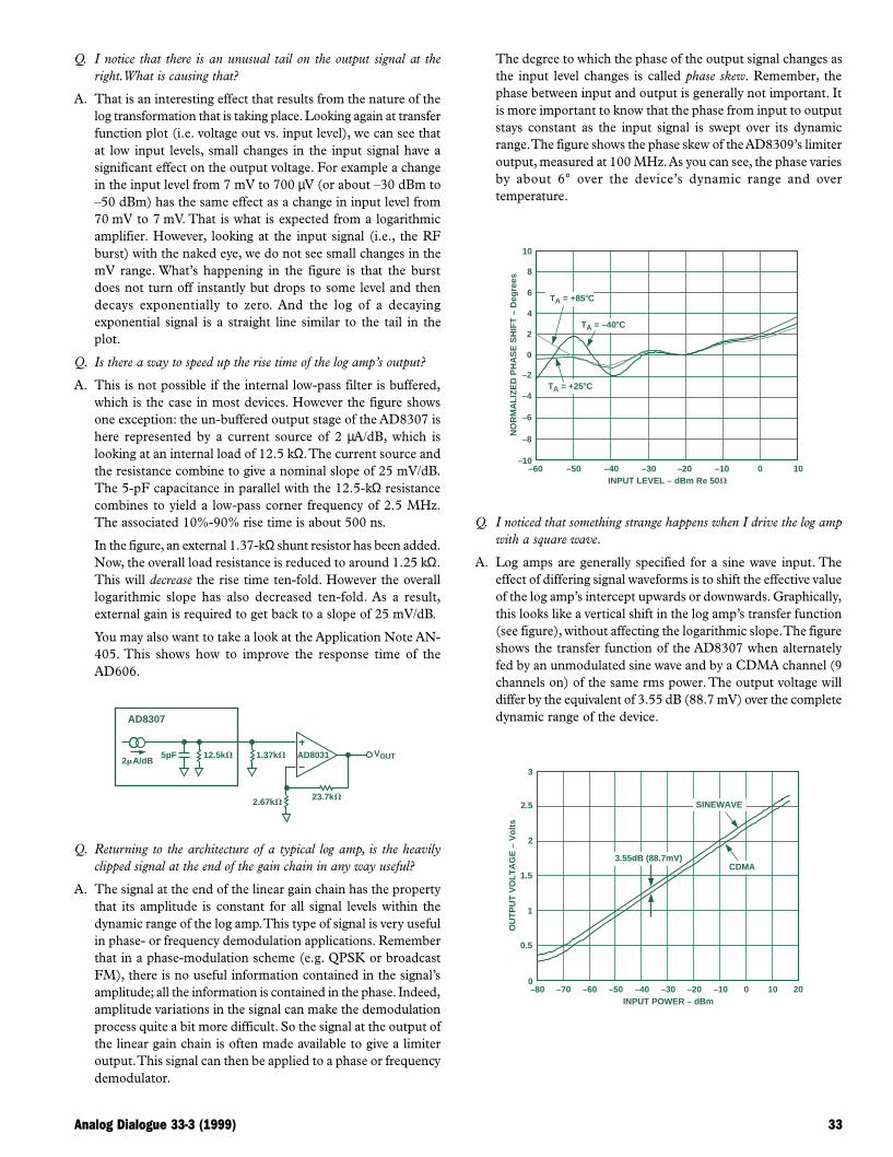
Analog Dialogue 33-3 (1999) 33
Q. I notice that there is an unusual tail on the output signal at theright. What is causing that?
A. That is an interesting effect that results from the nature of thelog transformation that is taking place. Looking again at transferfunction plot (i.e. voltage out vs. input level), we can see thatat low input levels, small changes in the input signal have asignificant effect on the output voltage. For example a changein the input level from 7 mV to 700 µV (or about –30 dBm to–50 dBm) has the same effect as a change in input level from70 mV to 7 mV. That is what is expected from a logarithmicamplifier. However, looking at the input signal (i.e., the RFburst) with the naked eye, we do not see small changes in themV range. What’s happening in the figure is that the burstdoes not turn off instantly but drops to some level and thendecays exponentially to zero. And the log of a decayingexponential signal is a straight line similar to the tail in theplot.
Q. Is there a way to speed up the rise time of the log amp’s output?
A. This is not possible if the internal low-pass filter is buffered,which is the case in most devices. However the figure showsone exception: the un-buffered output stage of the AD8307 ishere represented by a current source of 2 µA/dB, which islooking at an internal load of 12.5 kΩ. The current source andthe resistance combine to give a nominal slope of 25 mV/dB.The 5-pF capacitance in parallel with the 12.5-kΩ resistancecombines to yield a low-pass corner frequency of 2.5 MHz.The associated 10%-90% rise time is about 500 ns.
In the figure, an external 1.37-kΩ shunt resistor has been added.Now, the overall load resistance is reduced to around 1.25 kΩ.This will decrease the rise time ten-fold. However the overalllogarithmic slope has also decreased ten-fold. As a result,external gain is required to get back to a slope of 25 mV/dB.
You may also want to take a look at the Application Note AN-405. This shows how to improve the response time of theAD606.
AD8031
AD8307
12.5kV5pF2mA/dB
1.37kV
23.7kV2.67kV
VOUT
Q. Returning to the architecture of a typical log amp, is the heavilyclipped signal at the end of the gain chain in any way useful?
A. The signal at the end of the linear gain chain has the propertythat its amplitude is constant for all signal levels within thedynamic range of the log amp. This type of signal is very usefulin phase- or frequency demodulation applications. Rememberthat in a phase-modulation scheme (e.g. QPSK or broadcastFM), there is no useful information contained in the signal’samplitude; all the information is contained in the phase. Indeed,amplitude variations in the signal can make the demodulationprocess quite a bit more difficult. So the signal at the output ofthe linear gain chain is often made available to give a limiteroutput. This signal can then be applied to a phase or frequencydemodulator.
The degree to which the phase of the output signal changes asthe input level changes is called phase skew. Remember, thephase between input and output is generally not important. Itis more important to know that the phase from input to outputstays constant as the input signal is swept over its dynamicrange. The figure shows the phase skew of the AD8309’s limiteroutput, measured at 100 MHz. As you can see, the phase variesby about 6° over the device’s dynamic range and overtemperature.
INPUT LEVEL – dBm Re 50 V
10
–60
NO
RM
ALI
ZE
D P
HA
SE
SH
IFT
– D
egre
es
8
6
4
2
0
–10–50 –30 –20 –10 10
–2
–4
–6
–8
–40 0
TA = +858C
TA = +258C
TA = –408C
Q. I noticed that something strange happens when I drive the log ampwith a square wave.
A. Log amps are generally specified for a sine wave input. Theeffect of differing signal waveforms is to shift the effective valueof the log amp’s intercept upwards or downwards. Graphically,this looks like a vertical shift in the log amp’s transfer function(see figure), without affecting the logarithmic slope. The figureshows the transfer function of the AD8307 when alternatelyfed by an unmodulated sine wave and by a CDMA channel (9channels on) of the same rms power. The output voltage willdiffer by the equivalent of 3.55 dB (88.7 mV) over the completedynamic range of the device.
INPUT POWER – dBm
3
–60
OU
TP
UT
VO
LTA
GE
– V
olts
2.5
2
1.5
0–50 –30 –20 –10 10
1
0.5
–40 0–70–80 20
3.55dB (88.7mV)
SINEWAVE
CDMA

34 Analog Dialogue 33-3 (1999)
The table shows the correction factors that should be appliedto measure the rms signal strength of various signal types witha logarithmic amplifier which has been characterized using asine wave input. So, to measure the rms power of a squarewave,for example, the mV equivalent of the dB value given in thetable (–3.01 dB, which corresponds to 75.25 mV in the case ofthe AD8307) should be subtracted from the output voltage ofthe log amp.
Correction FactorSignal Type (Add to Output Reading)
Sine Wave 0 dB
Square Wave or DC –3.01 dB
Triangular Wave +0.9 dB
GSM Channel(All Time Slots On) +0.55 dB
CDMA Forward Link(Nine Channels On) +3.55 dB
Reverse CDMA Channel 0.5 dB
PDC Channel(All Time Slots On) +0.58 dB
Gaussian Noise +2.51 dB
Q. In your data sheets you sometimes give input levels in dBm andsometimes in dBV. Can you explain why?
A. Signal levels in communications applications are usuallyspecified in dBm. The dBm unit is defined as the power in dBrelative to 1 mW i.e.,
Power (dBm) = 10 log10 (Power/1 mW)
Since power in watts is equal to the rms voltage squared, dividedby the load impedance, we can also write this as
Power (dBm) = 10 log10 ((Vrms2/R)/1 mW)
It follows that 0 dBm occurs at 1 mW, 10 dBm corresponds to10 mW, +30 dBm corresponds to to 1 W, etc. Becauseimpedance is a component of this equation, it is alwaysnecessary to specify load impedance when talking about dBmlevels.
50VRIN(HIGH)
Log amps, however fundamentally respond to voltage, not topower. The input to a log amp is usually terminated with an
external 50-Ω resistor to give an overall input impedance ofapproximately 50 Ω, as shown in the figure (the log amp has arelatively high input impedance, typically in the 300 Ω to1000 Ω range). If the log amp is driven with a 200-Ω signaland the input is terminated in 200 Ω, the output voltage of thelog amp will be higher compared to the same amount of powerfrom a 50-Ω input signal. As a result, it is more useful to workwith the voltage at the log amp’s input. An appropriate unit,therefore, would be dBV, defined as the voltage level in dBrelative to 1 V, i.e.,
Voltage (dBV) = 20 log10 (Vrms/1 V)
However, there is disagreement in the industry as to whetherthe 1-V reference is 1 V peak (i.e., amplitude) or 1 V rms.Most lab instruments (e.g., signal generators, spectrumanalyzers) use 1 V rms as their reference. Based upon this,dBV readings are converted to dBm by adding 13 dB. So–13 dBV is equal to 0 dBm.
As a practical matter, the industry will continue to talk aboutinput levels to log amps in terms of dBm power levels, with theimplicit assumption that it is based on a 50 Ω impedance, evenif it is not completely correct to do so. As a result it is prudentto provide specifications in both dBm and dBV in data sheets.
The figure shows how mV, dBV, dBm and mW relate to eachother for a load impedance of 50 Ω. If the load impedancewere 20 Ω, for example, the V (rms), V (p-p) and dBV scaleswill be shifted downward relative to the dBm and mW scales.Also, the V (p-p) scale will shift relative to the V (rms) scale ifthe peak to rms ratio (also called crest factor) is somethingother than √2 (the peak to rms ratio of a sine wave). b
V (p-p) V (rms) dBV dBm mW
+10
+1
0.1
0.01
10
1
0.1
0.01
0.001 –60
–50
–40
–30
–20
–10
0
+10
+20
–50
–40
–30
–20
–10
0
+10
+20
+30
0.00001
0.0001
0.001
0.01
0.1
1
10
100
1000

Analog Dialogue 33-8 (1999) 35
Analog-to-DigitalConverter Architec-tures and Choices forSystem DesignBy Brian BlackHow important are the differences between sigma-delta andsuccessive-approximation architectures in choosing an analog-to-digital (A/D) converter? They can often be an important factor ininitiating the selection of a converter for a specific application. Wedescribe here four major circuit architectures used in A/D converter(ADC) design and outline the role they play in converter choicefor various kinds of applications. The descriptions are augmentedby three examples that illustrate tradeoffs and issues associatedwith architectural considerations.
Though not detailed or exhaustive, this overview is intendedto raise issues that should be understood when consideringconverters of different architectures. Sources of more-detailedinformation on converter architectures can be found in theReferences and at Internet sites indicated at appropriate points.As one might expect in a survey of this kind, these descriptionsare not comprehensive; and variations within each of thearchitecture families make generalizations less than fully accurate.Nevertheless, such generalizations are useful for the systemdesigner to keep in mind when conducting a high level overviewof a proposed system’s requirements.
CONVERTER ARCHITECTURESAn overwhelming variety of ADCs exist on the market today, withdiffering resolutions, bandwidths, accuracies, architectures,packaging, power requirements, and temperature ranges, as wellas hosts of specifications, covering a broad range of performanceneeds. And indeed, there exists a variety of applications in data-acquisition, communications, instrumentation, and interfacing forsignal processing, all having a host of differing requirements.
Considering architectures, for some applications just about anyarchitecture could work well; for others, there is a “best choice.”In some cases the choice is simple because there is a clear-cutadvantage to using one architecture over another. For example,pipelined converters are most popular for applications requiring athroughput rate of more than 5 MSPS with good resolution. Sigma-delta converters are usually the best choice when very highresolution (20 bits or more) is needed. But in some cases the choiceis more subtle. For example, the sigma-delta AD7722 and thesuccessive-approximations AD974 have similar resolution (16 bits)and throughput performance (200 kSPS). Yet the differences intheir underlying architectures make one or the other a betterchoice, depending on the application.
The most popular ADC architectures available today are successiveapproximations (sometimes called SAR because a successive-approximations (shift) register is the key defining element), flash(all decisions made simultaneously), pipelined (with multiple flashstages), and sigma-delta (Σ∆), a charge-balancing type. All A/Dconverters require one or more steps involving comparison of aninput signal with a reference. Figure 1 shows qualitatively how
flash, pipelined, and SAR architectures differ with respect to thenumber of comparators used vs. the number of comparison cyclesneeded to perform a conversion.
1
10
100
1,000
10,000FLASH
C = 2n –1t = 1
PIPELINEC P 3 2n/P
t = P
FLA
SH
16 BIT
12
10
5BIT
8 12 BIT16 BIT
SARC = 1t n
SUCCESSIVEAPPROXIMATION1 BIT
1 5 10 15DECISION CYCLES – t
NU
MB
ER
OF
CO
MP
AR
AT
OR
S –
C
8
10
1612
10
Figure 1. Tradeoff between decision cycles and comparators.
FLASH CONVERTERSConceptually, the flash architecture (illustrated in Figure 2) is quitestraightforward: a set of 2n–1 comparators is used to directlymeasure an analog signal to a resolution of n bits. For a 4-bit flashADC, the analog input is fed into 15 comparators , each of whichis biased to compare the input to a discrete transition value. Thesevalues are spaced one least-significant bit (LSB = FS/2n) apart.The comparator outputs simultaneously present 2n–1 discretedigital output states. If for example the input is just above 1/4 offull scale, all comparators biased to less than 1/4 full scale willoutput a digital “1,” and the others will output a digital “0.”Together, these outputs can be read much like a liquidthermometer. The final step is to level-decode the result intobinary form.
2n–1 (FULL SCALE)
.
.
.
AINLEVEL
DECODE
DIGITAL
2n
2n–2 (FULL SCALE)
2n
2 (FULL SCALE)
2n
1 (FULL SCALE)
2n
Figure 2. Basic flash architecture.
Design Considerations and Implications: The flash architecture hasthe advantage of being very fast, because the conversion occurs ina single ADC cycle. The disadvantage of this approach is that itrequires a large number of comparators that are carefully matchedand properly biased to ensure that the results are linear. Since thenumber of comparators needed for an n-bit resolution ADC isequal to 2n–1, limits of physical integration and input loading keepthe maximum resolution fairly low. For example, a 4-bit ADCrequires 15 comparators, an 8-bit ADC requires 255 comparators,and a 16-bit ADC would require 65,535 comparators! Formore about flash ADCs, see http://www.analog.com/supportstandard_linear/seminar_material/practical_design_techniques/Section4.pdf.

36 Analog Dialogue 33-8 (1999)
PIPELINED ARCHITECTUREThe pipelined (or pipelined-flash) architecture effectively overcomesthe limitations of the flash architecture. A pipelined converterdivides the conversion task into several consecutive stages. Eachof these stages, as shown in Figure 3, consists of a sample-and-hold circuit, an m-bit ADC (e.g., a flash converter), and an m-bitD/A converter (DAC). First the sample and hold circuit of thefirst stage acquires the signal. The m-bit flash converter thenconverts the sampled signal to digital data. The conversion resultforms the most significant bits of the digital output. This samedigital output is fed into an m-bit digital-to-analog converter, andits output is subtracted from the original sampled signal. Theresidual analog signal is then amplified and sent on to the nextstage in the pipeline to be sampled and converted as it was in thefirst stage. This process is repeated through as many stages as arenecessary to achieve the desired resolution. In principle, a pipelinedconverter with p pipeline stages, each with an m-bit flash converter,can produce a high-speed ADC with a resolution of n = p × m bitsusing p × (2m–1) comparators. For example, a 2-stage pipelinedconverter with 8-bit resolution requires 30 comparators, and a 4-stage 16-bit ADC requires only 60 comparators. In practice,however, a few additional bits are generated to provide for errorcorrection. For more about pipelined ADCs, See http://www.analog.com/support/standard_linear/seminar_material/practical_design_techniques/Section4.pdf.
ADC/COMPARATOR
DAC
DA
S
S+
–
++ D
SAMPLEAND HOLD
A
D
A
Figure 3. A single pipelined converter stage.
Design Considerations and Implications: Pipelined converters achievehigher resolutions than flash converters containing a similarnumber of comparators. This comes at the price of increasing thetotal conversion time from one cycle to p cycles. But since eachstage samples and holds its input, p conversions can be underwaysimultaneously. The total throughput can therefore be equal tothe throughput of a flash converter, i.e., one conversion per cycle.The difference is that for the pipelined converter, we have nowintroduced latency equal to p cycles. Another limitation of thepipelined architecture is that the conversion process generallyrequires a clock with a fixed period. Converting rapidly varyingnon-periodic signals on a traditional pipelined converter can bedifficult because the pipeline typically runs at a periodic rate.
SUCCESSIVE APPROXIMATIONSThe successive-approximations architecture can be thought of asbeing orthogonal to the flash architecture. While a flash converteruses many comparators to convert in a single cycle; a SARconverter, shown in Figure 4, conceptually uses a single comparatorover many cycles to make its conversion. The SAR converter workslike an old-fashioned balance scale. On one side of the scale, weplace the sampled unknown quantity. On the other side, we placea weight (generated by the SAR and DAC) that has the value of 1/
2 of full-scale and compare the two values. This first weightrepresents the most significant bit (MSB). If the unknown quantityis larger, the 1/2-scale weight is retained; if the unknown quantityis smaller, it is removed. This series of steps is repeated n times,using successively smaller weights in binary progression (e.g., 1/4,1/8, 1/16, 1/32, . . . 1/2n of full scale) until the desired resolution,n, is attained. Each weight represents a binary bit, with the largestrepresenting the most significant bit, and the smallest representingthe least significant bit.
ADCS–
+DIGITAL
A SAMPLEAND HOLD
SAR
DAC
Figure 4. Successive-approximations architecture.
Design Considerations and Implications: A SAR converter can use asingle comparator to realize a high resolution ADC. But it requiresn comparison cycles to achieve n-bit resolution, compared to pcycles for a pipelined converter and 1 cycle for a flash converter.Since a successive-approximations converter uses a fairly simplearchitecture employing a single SAR, comparator, and DAC, andthe conversion is not complete until all weights have been tested,only one conversion is processed during n comparison cycles. Forthis reason, SAR converters are more often used at lower speedsin higher-resolution applications. SAR converters are also wellsuited for applications that have non-periodic inputs, sinceconversions can be started at will. This feature makes the SARarchitecture ideal for converting a series of time-independentsignals. A single SAR converter and an input multiplexer aretypically less expensive to implement than several sigma-deltaconverters. With dither noise present, SAR and pipelined converterscan use averaging to increase the effective resolution of theconverter: for every doubling of sample rate, the effective resolutionimproves by 3 dB or 1/2 bit.
One consideration when using a SAR or pipelined converter isaliasing. The process of sampling a signal leads to aliasing—thefrequency-domain reflection of signals about the samplingfrequency. In most applications, aliasing is an unwanted effect thatrequires a low-pass anti-alias filter ahead of the ADC to removehigh-frequency noise components, which would be aliased intothe passband. However, undersampling can put aliasing to gooduse, most often in communications applications, to convert a high-frequency signal to a lower frequency. Undersampling is effectiveas long as the total bandwidth of a signal meets the Nyquistcriterion (less than one-half the sampling rate), and the converterhas sufficient acquisition and signal sampling performance at thehigher frequencies where the signal resides. While fast SARconverters are capable of undersampling, the faster pipelinedconverters tend to be more effective at it. For more aboutundersampling and dither, see http://www.analog.com/support/standard_linear/seminar_material/practical_design_techniques/Section5.pdf .
SIGMA-DELTAThe sigma-delta architecture takes a fundamentally differentapproach than those outlined above. In its most basic form, a sigma-delta converter consists of an integrator, a comparator, and a single-bit DAC, as shown in Figure 5. The output of the DAC is subtractedfrom the input signal. The resulting signal is then integrated, and

Analog Dialogue 33-8 (1999) 37
the integrator output voltage is converted to a single-bit digitaloutput (1 or 0) by the comparator. The resulting bit becomes theinput to the DAC, and the DAC’s output is subtracted from theADC input signal, etc. This closed-loop process is carried out at avery high “oversampled” rate. The digital data coming from theADC is a stream of “ones” and “zeros,” and the value of the signalis proportional to the density of digital “ones” coming from thecomparator. This bit stream data is then digitally filtered anddecimated to result in a binary-format output. For more aboutsigma-delta conversion, see http://www.analog.com/support/standard_linear/seminar_material/practical_design_techniques/Section3.pdf.
1-BITDAC
S–
+DIGITAL
DIGITALFILTER
ANDDECIMATOR
BITSTREAMD
COMPARATORINTEGRATOR
A E
Figure 5. Sigma-delta ADC architecture.
Design Considerations and Implications: One of the mostadvantageous features of the sigma-delta architecture is thecapability of noise shaping, a phenomenon by which much of thelow-frequency noise is effectively pushed up to higher frequenciesand out of the band of interest. As a result, the sigma-deltaarchitecture has been very popular for designing low-bandwidthhigh-resolution ADCs for precision measurement. Also, since theinput is sampled at a high “oversampled” rate, unlike the otherarchitectures described in this paper, the requirement for externalanti-alias filtering is greatly relaxed. A limitation of this architectureis its latency, which is substantially greater than that of the othertypes. Because of oversampling and latency, sigma-delta convertersare not often used in multiplexed signal applications. To avoidinterference between multiplexed signals, a delay at least equal tothe decimator’s total delay must occur between conversions. Thesecharacteristics can be improved in sophisticated sigma-delta ADCdesigns by using multiple integrator stages and/or multi-bit DACs.
APPLICATION EXAMPLESThe following three examples illustrate some of the issues describedabove.
Example 1: Multiple Inputs, 16-Bit ResolutionConsider an application that requires 16-bit resolutionfor 4 independent signals with bandwidths of dc to 15 kHz,15 kHz, 15 kHz, and 45 kHz. The total throughput required tosample these signals under the Nyquist criter ion is(2 × 15 + 2 × 15 + 2 × 15 + 2 × 45) kSPS = 180 kSPS. At firstglance, the SAR-type AD974, the sigma-delta AD7722, and thepipelined/sigma-delta AD9260 all have the required totalthroughput capability. But, as has been discussed above, theinherent latency of sigma-delta converters limits their effectivethroughput when they must continually acquire new signals bymultiplexing. Effective multiplexed throughput can be defined as thetotal throughput of a converter when two or more independentsignals are multiplexed. The following table compares the totalthroughput and effective throughput for each converter andindicates the number of converters of its type that would beneeded to serve in this application.
TotalThroughput Effective Converters (16-Bit Multiplexed Needed for
Converter Architecture Resolution) Throughput Application
AD974 SAR 200 kSPS 200 kSPS 1AD7722 Sigma-Delta 195 kSPS 2.3 kSPS 4AD9260 Pipelined/
Sigma-Delta 2500 kSPS 75 kSPS 3
Whether converting a single input or several multiplexed inputs,the AD974 achieves a throughput rate of up to 200 kSPS. Sincethe application requires a total throughput of 180 kSPS, theAD974’s performance is sufficient. In fact, this is exactly the typeof application that the AD974 was designed for: in addition to theSAR converter and reference, it also contains an integrated4-channel multiplexer.
The AD7722 and AD9260 both face the challenges confrontedby sigma-delta converters in multiplexing several inputs. TheAD7722’s throughput is 195 kSPS when sampling a single signal,but it drops to just 2.3 kSPS when converting multiple signals,due to the settling time which results from oversampling andfiltering. To use the AD7723 in this application, four converters(one per channel) would be needed.
The AD9260 combines pipeline and sigma-delta techniques. Itsthroughput rate of 2.5 MSPS makes it ideal for higher throughputsingle channel systems. But in this application, its settling time of13.35 ms limits its effective throughput to 75 kSPS. To use theAD9260 in this application would require at least 3 converters.Note that if the AD9260 were purely a pipelined flash converter, asingle converter would have had the required throughput, assumingthat the inputs are periodic.
Example 2: Single Input, 16-Bit ResolutionConsider now an application that converts a single 90-kHzbandwidth input at 16-bit resolution. In this case, all threeconverters from the first example would work well. Here the choiceamong converters would be made on other considerations,including ac and dc performance, system-level considerations (e.g.,Is there a great benefit to the anti-alias performance of sigma-delta converters in this application?), latency, and cost.
Example 3: Multiple Inputs, 14-Bit ResolutionConsider an application in which 16 inputs, each with a dc to100-kHz bandwidth, are converted with a resolution of at least 14bits. Three converters suitable for this application include the SAR-type AD7865, the sigma-delta AD7722, and the pipelined AD9240.The total throughput required under the Nyquist criterion is2 × 100 kHz × 16 = 3.2 MSPS. The following table shows thethroughput for each converter.
TotalThroughput Effective Converters (14-Bit Multiplexed Needed for
Converter Architecture Resolution) Throughput Application
AD7865 SAR 416 kSPS 416 kSPS 8AD7722 Sigma-Delta 220 kSPS 2.3 kSPS 16AD9240 Pipelined 10 MSPS 10 MSPS 1
Of the three converters, only the AD9240 has the throughputneeded to convert all 16 channels. The AD7865 has sufficientthroughput for 2 inputs per converter. To use the AD7865 in thisapplication, 8 converters would be needed. The AD7722 would

38 Analog Dialogue 33-8 (1999)
need to be used in a converter-per-channel implementation; thus16 converters would be required.
SummaryWhile not exhaustive, the following table summarizes and ranks(in a generalized sense) the relative advantages of flash, pipelined,SAR, and sigma-delta architectures. A rank of 1 in a performancecategory indicates that the architecture is inherently better thanthe others for that category. An * indicates that the architecturehas the capability or characteristic listed.
Sigma-Characteristic Flash Pipelined SAR Delta
Throughput 1 2 3 4Resolution (ENOB) 4 3 2 1Latency 1 3 2 4Suitability for converting multiple
signals per ADC 1 2 1 3Capability to convert non-periodic
multiplexed signals 1 2 1 3Simplified anti-aliasing *Can undersample * * *Can increase resolution through
averaging (with dither noise) * * *
ACKNOWLEDGMENTThe author is indebted to Alain Guery and Mike Coln for providingvaluable direction, and for providing the figures shown.
REFERENCESAnalog-Digital Conversion Handbook, The Engineering Staffof Analog Devices, Inc. Englewood Cliffs, NJ: Prentice Hall,1986. ISBN 0-13-032848-0. Available from Analog Devices:Phone (781) 461-3392.
Practical Analog Design Techniques, edited by Walt Kester. Norwood,MA: Analog Devices, Inc., 1995. ISBN 0-916550-16-8. Availablefrom Analog Devices: Phone (781) 461-3392. Also available freeon the Internet as PDF chapters. http://www.analog.com/support/standard_linear/seminar_material/index.html
High Speed Design Techniques, edited by Walt Kester. Norwood, MA:Analog Devices, Inc., 1996. ISBN 0-916550-17-6. Available fromAnalog Devices: Phone (781) 461-3392. Also available free on theInternet as PDF chapters. http://www.analog.com/support/standard_linear/seminar_material/index.html
Linear Design Seminar, edited by Walt Kester. Norwood, MA:Analog Devices, Inc., 1995. ISBN 0-916550-15-X. Available fromAnalog Devices: Phone (781) 461-3392. b
CCD SIGNAL PROCESSORThe first true 14-bit CCD processor with 3-channel input anddigitizerThe AD9814 is a 14-bit, 3-channel analog signal processor anddigitizer designed for high-performance 3-channel 10 MSPS tri-linear CCD imaging applications, such as color film- and documentscanners. Each channel includes an input clamp, correlated doublesampler (CDS), 9-bit offset DAC, and 6-bit programmable-gainamplifier (PGA), multiplexer, and 14-bit ADC. The output is apair of 8-bit multiplexed words, accessed by two Read cycles. Thedevice is programmed via a serial interface. The true-14-bit K gradeguarantees no missing codes, maximum differential nonlinearityof ±1 LSB, and the lowest noise in the industry. The device ishoused in a 28-lead 0.3" SOIC, operates from 0°C to +70°C, andrequires a 3.0 to 5.25 V supply. Prices in 100s (K/J versions) are$29.50 and $11.15.
AFE FOR FLAT-PANEL DISPLAYSFirst Integrated Analog Interface for SXGA Flat PanelDisplays (100 MSPS/140 MSPS)The AD9884A is the World’s first integrated analog interface forSXGA flat-panel displays. Integrating a triple 140 MSPS A/Dconverter, PLL, and preamplifiers, it is a monolithic analoginterface optimized for digitizing RGB graphics signals frompersonal computers and workstations. Its 140 MSPS encode-ratecapability, with 500 MHz full-power analog bandwidth, supportsdisplay resolutions of up to 128031024 at 75 Hz with sufficientbandwidth to accurately acquire and digitize each pixel. Operatingon a 3.3 V supply, it dissipates less than 650 mW. Its signal-tonoise ratio is better than 46 dB at 20 MHz inputs. Operating from0 to +70°C, it is available in 128-pin MQFP packages in twosampling-rate grades, 100 MSPS (XGA) and 140 MSPS (SXGA),priced at $21 and $25.50 in 1000s. An evaluation board is available.
New-Product Briefs
9-BITDAC
PGACDS
PGA
9-BITDAC
CDS
9-BITDAC
PGACDS
3:1MUX
14-BITADC
14 14:8MUX
8
BANDGAPREFERENCE
CONFIGURATIONREGISTER
MUXREGISTER
BLUEGREEN
RED
BLUEGREEN
RED
6
9
GAINREGISTERS
OFFSETREGISTERS
DIGITALCONTROL
INTERFACE
INPUTCLAMP
BIAS
AD9814
DRVDD DRVSSAVDD AVSSCAPT CAPBAVDD AVSS CML
OEB
DOUT
SCLK
SLOAD
SDATA
ADCCLKCDSCLK2CDSCLK1
OFFSET
VINB
VING
VINR
SDA SCL A0 A1 PWRDN
HSYNC
COAST
CLAMP
FILT
CKEXT REFINCKINV
REFOUT
8A/DCLAMPRIN
GIN
BIN
8A/DCLAMP
8
8A/DCLAMP
8
REF
8
8
8
8
8
8
SOGIN
0.15V
2
AD9884A
CLOCKGENERATOR
SOGOUT
DATACK
ROUTA
ROUTB
GOUTA
GOUTB
BOUTA
BOUTB
HSOUT
CONTROL
Analog Dialogue 33-4 (1999) 39
New TxDAC®
Generation125-MSPS 10-, 12-, and14-bit high-performanceDACs for widebandmultitone communicationTransmit channels
150pF+1.20V REF
AVDD ACOMREFLO
ICOMPCURRENTSOURCEARRAY
+5V
SEGMENTEDSWITCHES
LSBSWITCHES
REFIOFS ADJ
DVDD
DCOM
CLOCK
+5VRSET
0.1mF
CLOCK
IOUTA
IOUTB
0.1mF
LATCHES
AD9754
SLEEP
DIGITAL DATA INPUTS (DB13–DB0)
Figure 1. AD9754 functional block diagram.
The AD9754, AD9752, and AD9750 are 14-, 12-, and 10-bitwideband, high-performance, low-power CMOS digital-to-analogconverters that operate from +5 V supplies. They offer exceptionalac and dc performance, while supporting update rates up to125 MSPS. All three share the same interface options, 28-leadTSSOP or 0.3" small-outline package, and pinout as the firstgeneration, the AD976x series [Analog Dialogue 30-3, 1996, pp. 3-5].This allows a highly flexible upward or downward selection path,based on performance, resolution, and cost.
These DACs are current-output; they have a nominal 20-mA full-scale output with a 100-kΩ source impedance and 1.25-Vcompliance range. The outputs are differential to support eitherdifferential or single-ended applications. The devices include aninternal 1.20-V reference and a control amplifier which can setoutput full-scale values from 2 mA for power conservation to20 mA, providing 20 dB of output flexibility. They have lowdissipation of 190 mW, which can be reduced to 65 mW at the2-mA end of the output scale, and just 20 mW in power-downmode. They are equipped with edge-triggered latches, and thedigital interface is CMOS compatible (+2.7 to 5.5 V)
Emerging wireless/wireline communications standards (Wideband,Multicarrier) are demanding lower distortion and noise to improvesystem capacity and signal quality. The D/A converter in a modem/transceiver transmitting chain (TxDAC) is the basic analog signalgenerator; it defines the ultimate performance available in acommunications system. Everything after it—power amplifier,antenna, transmission medium, and receiver front end—can onlycontribute to the degradation of a digitally defined signal, and the
end result can never be better than what is at first available fromthe TxDAC.
The AD975x family is specifically designed for applications suchas wideband CDMA, software/multi-carrier base stations, wirelesslocal-loop RIUs, wireless LAN, broadband set-top boxes, andxDSL modems that utilize wide signal bandwidths to transmit highvolumes of data over a desired medium. Key specifications over a25-MHz band, such as 68-dBc SFDR (spurious-free dynamicrange) and –65-dBc THD (total harmonic distortion), are improvedover those of the AD976x family by 8 to 10 dB, accompanied by a9-dB lower integrated noise floor at –109 dB.
The AD975x DACs operate over the industrial temperature rangefrom –40 to +85°C. Evaluation boards are available. Prices* (1000s)for 14/12/10 bits are $21.09/$16.70/$9.45.
What’s special about DACs for multitone?The frequency-domain performance of high-speed DACs hastraditionally been characterized by analyzing the spectral outputof a reconstructed full-scale (i.e., 0 dB FS) single-tone sine waveat a particular output frequency and update rate. Although thischaracterization data is useful, it is often insufficient to reflect aDAC’s performance for a reconstructed multitone or spread-spectrum waveform. In fact, evaluating a DAC’s spectralperformance using a full-scale single-tone at the highest specifiedfrequency (i.e., fH) of a bandlimited waveform is typically indicativeof a DAC’s “worst-case” performance for that given waveform. Inthe time domain, the full-scale sine wave represents the lowestpeak-to-rms crest factor (i.e., VPEAK/VRMS) that the bandlimitedsignal will encounter.
However, the inherent nature of a multitone, spread-spectrum, orQAM waveform, in which the spectral energy of the waveform isspread over a designated bandwidth, will result in a higher peak-to-rms ratio when compared to the case of a simple sine wave. Asthe reconstructed waveform’s peak-to-average ratio increases, anincreasing amount of the signal energy is concentrated around theDAC’s midscale value. Figure 2 is just one example of a bandlimitedmultitone vector (i.e., eight tones) centered on one-half the Nyquistbandwidth (i.e., fCLOCK/4).
MA
GN
ITU
DE
– d
Bm
FREQUENCY – MHz
–10
–70
–1102.19 2.812.25 2.31 2.38 2.44 2.50 2.56 2.63 2.69 2.75
–20
–60
–80
–100
–40
–50
–90
–30
Figure 2. Multitone spectral plot.
This particular multitone vector has a peak-to-rms ratio of 13.5 dB,as compared to a sine wave’s peak-to-rms ratio of 3 dB. This meansthat the DAC must be able to handle a waveform where most of
*Prices indicated here are recommended resale prices (U.S. Dollars) FOB U.S.A.Prices are subject to change without notice. For specific price quotations, getin touch with our sales offices or distributors.

40 Analog Dialogue 33-4 (1999)
the information is carried at low levels in order to be able to handlelarge instantaneous peaks without clipping. A “snapshot” of thisreconstructed multitone vector in the time domain as shown inFigure 3 reveals the dense signal content around the midscale value.As a result, a DAC’s “small-scale” dynamic and static linearitybecome increasingly critical to obtaining low intermodulationdistortion and maintaining sufficient carrier-to-noise ratios for agiven modulation scheme.
TIME
1.0000
0.8000
–1.0000
VO
LTS
–0.2000
–0.4000
–0.6000
–0.8000
0.2000
0.0000
0.4000
0.6000
Figure 3. Time-domain “snapshot” of the multitone waveform.
A DAC’s small-scale linearity performance is also an importantconsideration in applications where additive dynamic range isrequired for gain-control purposes or “predistortion” signalconditioning. For instance, a DAC with sufficient dynamic rangecan be used to provide additional digitally controlled variation ofits reconstructed signal. In fact, the gain can be controlled in6-dB increments by simply performing a shift-left or -right on theDAC’s digital input word. An application might be to predistortthe DAC’s input signal intentionally to compensate fornonlinearities associated with subsequent analog components inthe signal chain. For example, the signal compression associatedwith a power amplifier can be compensated for by predistortingthe DAC’s digital input with the inverse nonlinear transfer functionof the power amplifier. Since the DAC must accommodateincreased gains at higher output levels, the DAC’s performance atreduced signal levels should be carefully evaluated.
A full-scale single tone will induce all of the dynamic and staticnonlinearities present in a DAC that contribute to its distortion;the distortion components will reduce its SFDR (Spurious-freedynamic range). Thus, in Figure 4 as the frequency of the digitallygenerated single-tone waveform increases, the dynamic linearities
of a DAC (here the AD9754) tend to dominate, thus contributingto the substantial reduction in SFDR with increased frequency.
fOUT – MHz
SF
DR
– d
B
90
80
400.1 1001 10
60
70
5MSPS 25MSPS
65MSPS
50MSPS
125MSPS
50
Figure 4. AD9754 SFDR vs. fOUT @ 0 dB FS.
However, unlike the vast majority of DACs, which employ anR-2R ladder for the lower-bit current segmentation, the AD9754(and the other TxDACs) actually exhibit an improvement indistortion performance as the amplitude of a single tone is reducedfrom its full-scale level. This reduction of distortion at reducedsignal levels is evident in the SFDR plot of Figure 5, whichshows typical SFDR vs. frequency at 0, -6, and -12 dB levels for a65-MSPS sampling rate. Maintaining such decent “small-scale”linearity across the full span of a DAC transfer function is criticalin maintaining excellent multitone performance. b
fOUT – MHz
SF
DR
– d
Bc
90
400 5 3010 15 20
80
70
60
0dBFS
–6dBFS –12dBFS
25
50
Figure 5. AD9754 SFDR vs. fOUT at 65 MSPS.
D/A CONVERTER14-Bit, 150 MSPS TxDAC+® with 23 Interpolation Filter
The AD9772 is the first DAC to be able to do direct IF synthesisin the 75–140 MHz frequency range. It is a single-supply, 14-bitD/A converter with differential current outputs, optimized forbaseband or IF waveform reconstruction applications requiringexceptional dynamic range. It is designed for communicationTransmit channels, such as WCDMA base stations, multicarrierbase stations, and direct IF synthesis. It integrates a complete,
low-distortion 14-bit DAC with a 23 interpolation filter and aPLL clock multiplier with a flexible differential clock-driver inputfor single-ended or differential clock drive and optimum jitterperformance. The AD9772 can reconstruct full-scale waveformswith bandwidths as high as 63.3 MHz while operating at an inputdata rate of 150 MSPS. It operates from a single 2.7 V to 3.6 Vsupply, dissipates only 205 mW (13 mW in Power-down), isavailable in a 48-lead LQFP package, and operates from –40 to+85°C. Price is $32.18 in 1000s.
New-Product Brief

Analog Dialogue 33-5 (1999) 41
Ultrasound AnalogElectronics Primerby Bill Odom
INTRODUCTIONModern technology is driving medical ultrasound machines to newheights of performance, resulting in images with new levels of clarityand resolution. Ultrasound is used for imaging in cardiac, obstetric,and many other diagnostic areas. Even as the abilities of themachines increase, the cost of machines is coming down. Althoughultrasound relies substantially on digital processing, the key to itsperformance lies in a heavily analog technology. We will examinehere the contributions of the analog and mixed-signal componentsused in ultrasound imaging. Naturally, since each element wouldby itself need a chapter or a book of its own to provide fully usefulinformation for the system designer, this article is intended toprovide an overview and furnish a basic understanding of medicalultrasound architecture. Though this article will barely scratch thesurface of design objectives and rules; some of the issues to beraised will have relevance in a broader context of applications andare likely to be examined in greater detail in future articles.
Obtaining an ImageImages are obtained by sweeping a narrow beam of acoustic energyinto a living body and analyzing the pattern of the energy reflectedback by structures within the body, much like a search radar. Sincethe receiving transducers are dealing with analog signals, but theanalysis is performed digitally, the signals must be digitized.Electrical pulses are applied to piezoelectric ceramic elements togenerate the energy at transmitted frequencies from 2 to 20 MHz.The frequency used depends on the application. Higher frequenciesprovide the best resolution but have less penetration, since theyattenuate faster as the signals move through the body. There arelimits on how strong the high-frequency pulse can be, becauseexcessive amounts of power are unhealthy for the patient. The mostcommonly used frequencies range from 2 to 7 MHz.
Return levels range from 1-V echoes near the surface of the bodyto less than 10 µV for images deep within the body. The signals areconducted to and from the ceramic elements in the hand piece tothe front-end electronics via a cable, which will be subject to noiseand attenuation. The wide range of signals must be amplified to2 V for driving an analog-to-digital converter. To accomplish this,a time-gain compensation (TGC) amplifier is used. It will compensatefor exponential signal decay by amplifying the signal by anexponential factor that depends on how long the machine has beenwaiting for the return pulse.
Power levels, frequencies used, amplification, and beam focusdetermine the clarity of the image. These things are controlled bythe sonographer (technician), interacting with the system’s inherentproperties.
Imaging Modes Used1. Gray scale—produces a basic black-and-white image. It will
resolve artifacts a small as 1 mm. The display is made bytransmitting bursts of energy and analyzing the return energy(as mentioned above).
2. Doppler—The best analogy to medical Doppler ultrasound iscolor Doppler weather radar. As the name suggests, Doppler
modes detect the velocity of an object in motion by trackingthe frequency shift of the return signal. These principles areapplied in examining blood or other fluids flowing within thebody. It is accomplished by transmitting a continuous waveinto the body and producing a fast Fourier transform (FFT) ofthe return. The computational process will determine thefrequency components of the signals from the body and theirrelationship as a function of fluid velocity. One bin will containthe fundamental transmitted frequency while other bins containthe Doppler shifted frequencies. 4× oversampling is oftenemployed.
3. Venous and arterial modes—They employ Doppler in conjunctionwith the gray-scale mode. First the image of a vein or arterywill be found. The operator will dial in a small cursor windowaround it. The Doppler is then engaged within the cursor area.The transmitted signal’s Doppler frequency shift will bemeasured as discussed above. Audio will also be used with thecursor image. Venous flow produces a rushing sound (like awaterfall), while the thump of a pulse will indicate arterial flow.At the same time, blood velocity will be displayed on a digitalreadout. The sinus rhythm will be displayed as an X-Y plot onthe screen. The velocity and rhythm displays are obtained byprocessing the audio signal from the Doppler shifts.
The Overall SystemThe block diagram (Figure 1) shows the elements of a system:transducer, multiplexer, transmitter and its beam-formingapparatus, transmit/receive (T/R) switches, low-noise amplifier,signal- and image-processing display, audio, A/D converter andits driver, the TGC amplifier. At the current state of the art,machines can employ as many as 256 channels (comprising 256ceramic elements, amplifiers, ADCs, etc.).
TXBEAMFORMER
MUX ANDT/R SWITCHES
BEAMFORMERCENTRAL CONTROL
SYSTEM
ADC RXBEAMFORMER
SPECTRALDOPPLER
PROCESSING(D MODE)
IMAGE &MOTION
PROCESSING(B MODE)
COLORDOPPLER
PROCESSING(F MODE)
AUDIOOUTPUT
DISPLAY
CABLETGCAMPLIFIER
HVTX AMPs
Figure 1. System block diagram.
Probes and Their Transmitted SignalsThe probes will have a ceramic element for each channel (up to256). The elements are made of a piezoelectric ceramic materialsuch as lead zirconium titanate.
In some designs the pulses ring in bursts of a few cycles each timethey get a short transmit pulse of about 100 ns (“ping and ring”).The excitation pulse amplitudes will be of the order of 100 V.The magnitude of the pulse will determine the amount of energybeamed into the patient.

42 Analog Dialogue 33-5 (1999)
In order to minimize distortion, some systems transmit a Gaussianpulse. Figure 2 contrasts the distorted spectrum of a broadbandpulse after it is bounced around in the body. Its spectrum bearslittle resemblance to that of the transmitted pulse. The misshapenpulse will show harmonic distortion and unwanted spuriousartifacts. On the other hand, the response to a transmitted Gaussianpulse spectrum looks much the same as when it went out, free ofside lobes.
TRANSMITTEDPULSE
RECEIVEDPULSE
TRANSMITTEDPULSE
RECEIVEDPULSE
Figure 2. Waveform types (simplified): Gaussian burst,reflected flat-top pulse, and reflected Gaussian pulse.
The excitation pulse might be the output of a DAC, with the signalgiven the desired shape by a digital synthesizer. The low amplitudepulse will then be amplified to the required amplitude(approximately 100 V).
The receiver must have a wide bandwidth to accommodate thewide range of complex frequencies that must be handled in theDSP’s FFT computation. Fast edge rates increase the demand forbandwidth.
Beam Steering and FocusIn the old days of radar, a dish or a banana-shaped antenna wouldrotate, looking for targets in all directions. As it slowly swept around,a magnetron would fire pulses of energy into the sky. Traveling atthe speed of light, reflected energy would come back to the receiverbefore the antenna moved out of sync. Nowadays, the rotation isproduced by phased arrays. The beam is manipulated by varyingthe phase and power of the signal between antenna radiators, andthe beam is swept around the sky without any moving parts.
This is the same method used by medical ultrasound to sweep abeam of acoustic energy around the body. There will beprogrammed phase and amplitude shifts between the pulses ofenergy delivered to the piezoelectric elements arrayed in thetransducer head. This will result in an incident beam of energydirected along a line into the body. The beam will be swept backand forth in the body like the radar across the sky.
Mux and T/R SwitchThe signals to be transmitted must pass from the power amplifierto ceramics and the received signal from ceramics to the receiver.Since the 100-V Transmit and microvolt-level Receive signal mustpass through the same cable, a T/R switch (transmit/receive) andmultiplexer (mux) are required to steer the signals.
Receiver Beam FormingThe beam is focused by delaying each of the channels so that thereturn pulses from the focal point (or area) arrive at the processorat the same time (see Figure 3). The machine will establish thefocal area as set by the operator. Beam forming is currently donewith both analog and digital techniques. The machine will adjustthe delay required for focus in calculating the position of the sweepline. It will compute the corresponding pixels of the display byusing the delay required by each channel to focus the image. Newermachines have multiple focus zones.
Time Gain Control (TGC)The TGC (time gain compensation) amplifier is a crucial link inthe ultrasound signal path. It must have the ability to amplify signals
ranging from a few microvolts to 1 volt up to one or two volts forthe ADC. This gain will be exponentially increased along eachtransmit/receive sweep line. At the near end of the wedge, the gainwill be very low. It will have to process the 1-V return signal rightafter the 100-V ceramic excitation pulse. As time after the excitationpulse passes, the gain will be swept into very high levels. This mustbe done while maintaining very low noise to avoid masking low-level signal coming from deep within the body. The operator willadjust the TGC amplifier control to improve the quality of theimage. The AD604 <http://products.analog.com/products/info.asp?product=AD604> variable-gain amplifier, widely used inthis application, has two channels that can accept a linear timesweep and produce an exponentially increasing gain with a 48-dBrange (power ratio approaching 100,000:1).
The A/D ConverterThere are many sources of noise that combine at the input of theADC, including body tissue, gain stages and cable noise. As thelast link in the chain, it is important that the ADC itself have lownoise. Its noise must not be confused with the surviving signalcoming from the other components. Quantization noise is improvedby using higher resolution converters. Many ultrasound systemsuse 10-bit converters with theoretical quantization noise of-61.7dB. Newer machines are using 12-bit converters, which bringthe theoretical quantization noise down to <–73dB.
Many ultrasound designers are concerned with harmonic distortionand artifacts at frequencies close to the fundamental. Unlike astate trooper’s Doppler radar, which deals with a large frequencyshift when measuring the velocity of a speeding Honda, the Dopplermodes of an ultrasound system measuring the velocity of blood ina vein or artery produce a shift of only a few hertz. In the FFTplot, the areas near the base of the fundamental frequency spikemust be very quiet and free of spurious signals, often caused byADC or system clock jitter, so as not to mask out this shift. Linearityof the converter is also important to the quality of Dopplerultrasound.
Low intermodulation distortion in an ADC will help to preventthe various harmonic artifacts of Doppler return from mixing toform aliases or adding to form large spurs. The reflected signalsinside the body can be considered as multi-tone signals. If theADC has poor harmonic distortion characteristics, the tones willcombine with the ADC’s harmonics, which could dwarf a low-amplitude return signal.
Many ultrasound manufactures use 4× oversampling for improvingsignal-to-noise and to reduce complexity in antialias filters.However, a 12-MHz mammography machine will need better than48 MHz to accommodate the system. Oversampling rates aredictated by the ability of the signal processing chain to process thedata stream.
VARIABLE DELAYS ARRAY
FOCALPOINT
PROCESSING
Figure 3. Beam focus using variable delay.

Analog Dialogue 33-5 (1999) 43
DisplayOnce the points have been scanned, they must be displayed. Nowconsider how the machine places the images on the screen. It willcalculate the location of a target on the screen based on the timedelays from element to element in the row of ceramics in the handpiece. It judges depth based on how long it took the signal to comeback from each ceramic element. The pixel values will be read outof memory and modulate the CRT trace.
The machine must compute the location of each point and addcolor. Perhaps it will average several received scans together. Thenit will start the CRT sweep at the top of the fan-shaped display.
Harmonic ImagingTo gain the improved resolution from higher-frequency, whileameliorating the dilemma of depth of penetration vs. energy level,harmonic imaging is used. Harmonic imaging gathers increasedresolution by processing the second harmonic of the fundamentaltransmit pulse. The harmonic is generated by the tissue itself orthe use of contrasting agents injected into the tissue. Thistechnology will put the pressure on amplifiers and ADCs tominimize additional harmonics by maintaining low harmonicdistortion.
Future Component RequirementsThere is an ongoing demand for lower power components. In earlierdays in hospitals, portable meant that the bulky machine had bigwheels, and that it could be powered from the 120-V/15-ampreceptacle in a hospital room rather than the 220-V/30-Areceptacles in Radiology. Nowadays, there is growing interest ininstalling ultrasound in emergency vehicles and making it reallyportable. Tendencies in component design support suchmomentum. For example previous high-speed 10-bit ADCs drew> 400 mW. That’s a lot of power when there are 256 converters in
close quarters. In contrast, the 10-bit, 40-MSPS AD9203<http://products.analog.com/products/info.asp?product=AD9203>draws just 75 mW.
Cost has come down more than 2 to 3× from levels of a fewyears ago. This makes practical the use of higher-resolution,faster ADCs, such as the low-cost, 12-bit 65-MHz AD9226<http://products.analog.com/products/info.asp?product=AD9226>.
More Things to ComeAs time goes on it is logical to expect better images for less money.This will be made possible by ADC’s with even higher resolutionsand data rates. Many more samples can be made of reflected imagesas they arrive at the processor.
3-D imaging is now being developed. With these machines onecan get a better overall view of an image, which can result in quickerand more accurate diagnosis and less unnecessary surgery.
More InformationMost ultrasound manufacturers maintain web sites <http://dir.yahoo.com/Business_and_Economy/Companies/Health/Medical_Equipment/Ultrasound/>. There are many technicalarticles and application notes available <http://dir.yahoo.com/Health/Medicine/Medical_Imaging/Ultrasound/>. Logisticsprohibited the reproduction of ultrasound images here, but thereare many available in cyberspace1. Be sure and check out 3-Dimages, they are awesome. So are the prospects for morewidespread use of ultrasound as a rapidly maturing noninvasiveimaging technology. b
1http://home.hkstar.com/~joewoo/joewoo2.html
The author is indebted to Eberhard Brunner for conceiving the drawings usedhere.
POWER MANAGEMENTGeyserville-Enabled DC/DC Converter Controller for MobileCPUs
The ADP3421 is a hysteretic voltage-programmed dc-to-dc buckconverter controller with two auxiliary linear regulator controllers.It provides a total power conversion-control solution for amicroprocessor, by delivering the core, I/O, and clock voltages.The main output voltage is set by a 5-bit VID code. The ADP3421features high-speed operation to minimize the size of the externalinductors, resulting in the fastest change of current to the output.It also features optimally compensated active voltage positioningto minimize the size of the output capacitors while providingsuperior load transient response. The ADP3421 is specified for a3.3-V supply, and it draws only 10 mA max in shutdown. Themain output signal interfaces with the ADP3410 dual MOSFETdriver. The ADP3421 is packaged in a 28-lead TSSOP, and operatesover the 0 to +100° C temperature range. Price (1000s) is $2.50.
New-Product Brief
VHYS
VID3
VID4
LTB
LTI
LTO
CLSET
VID2
VID1
VID0
CLKDRV
CLKFB
IODRV
IOFB
CS–
GND
OUT
VCC
RAMP
REG
CS+
DACOUT
CORE
SSC
SSL
UVLO
PWRGD
SD
LEVELTRANSLATOR
EN
CORECOMPARATOR
CORE CONTROLLER
ADP3421
CLOCK LDOCONTROLLER
I/O LDOCONTROLLER
VIN/VCCMONITOR AND
UVLO BIASREFERENCE
CONTROLLER
BIAS ANDREFERENCE
SOFT STARTTIMERAND
POWER GOODGENERATOR
BIAS EN
VID DAC
CURRENTLIMIT
COMPARATOR

44 Analog Dialogue 33-1 (1999)
A Chip You Can Use toMonitor EnvironmentalConditions on PCMotherboard Designsby Matt SmithManagement of the electrical, mechanical, and thermalenvironment is of growing importance in today’smicroprocessor based systems. This article will focus onaccurate voltage and temperature monitoring as well asserving other hardware monitoring requirements. We willconsider techniques for making accurate measurementsand offer solutions for the range of hardware monitoringtasks in Pentium II-based systems as embodied in theADM9240 chip.
As designers of ICs and systems seek to squeeze every last morselof performance out of their designs, hardware monitoring andcontrol have become an integral part of circuit board designobjectives. Examples include the need to maintain accurate supplyvoltage levels and continually dispose of the heat generated byhigh-performance chips. The feedback portion of the control loopis accomplished by hardware monitoring —the continuousmeasurement of critical system parameters, such as power supplyvoltages, internal temperatures, cooling fan performance, and otherenvironmental factors. System performance can be maximized byclosely controlling these parameters to remain within tight limitsso as to maintain optimum operating conditions for the circuitryand avoid reduction of component life.
The latest generation of Intel1 Pentium-based products clearlydemonstrates the importance of hardware monitoring and control.The newest Pentium II microprocessors running with clock ratesin excess of 450 MHz require complex, highly regulated supplyvoltages—a simple +5 or +3.3-V power supply no longer suffices.Instead, the Pentium core logic demands digitally adjustablevoltages ranging from 1.3 to 3.5 V with 50-mV resolution. Theactual voltage required depends on a number of factors. Controllingthe voltage to this degree is not a trivial requirement when oneconsiders the dynamically varying nature of the currents flowingthrough the resistance and inductance of the printed-circuit-board(PCB) traces. In addition to the requirements of the processorchip, a typical system will require at least 4 other regulated supplies,+12 V, –12 V, +5 V, and +3.3 V, for other functions, such as diskdrives, video circuitry, PC cards, etc. In order to maintain long-term reliability, all these voltages must be accurately monitoredand controlled. Simple voltage-comparator types of circuits canbe used to monitor fixed supplies; but monitoring variably loadedhigh-accuracy supplies requires more sophisticated solutionsinvolving analog-to-digital conversion of voltage levels.
Besides tightly controlled operating voltages, many of today’ssystems also rely on thermal management approaches, such as thecooling provided by active heat sinking, convection cooling andforced air cooling to maintain reliable operating conditions. AsICs and systems become increasingly faster, more complex, and
1All brand or product names mentioned are trademarks or registered trade-marks of their respective holders.
more dense, removing the excess heat and maintaining safe, reliableoperating temperatures has become increasingly important.Temperature sensing, often coupled with fan-speed monitoringand control, are a couple of the techniques being employed todayto ensure system reliability. By controlling fan speed, greaterefficiency, reduced power dissipation and lowered noise levels areachieved.
Another important area that benefits by effective hardwaremonitoring is total cost of ownership (TCO). All the vital functionsare monitored continuously and the results communicated to thesystems management software. Impending failures can be detected,the sources identified, and corrective action taken—or even systemshutdown invoked—before expensive damage occurs. For example,a clogged-up cooling fan may be detected by monitoring its speed.When the speed has decreased by 10 to 15% from its nominalspeed, the software can note the problem and shut down the systembefore the deterioration has caused additional damage. Replacinga fan for $10 is more appealing than replacing a $1000 CPU or aneven more-expensive system board.
Multi-channel voltage, temperature and fan-speed monitoring,together with programmable limit-setting for each of theseparameters, goes a long way towards meeting the monitoring andcontrol objective. We will discuss below some specific techniquesfor achieving this in Pentium-based systems. The demonstrationwill employ a new monitoring IC, ADM9240, from Analog Devices,to show approaches to optimizing the monitoring strategy.
Voltage MonitoringAs many as six voltage channels require monitoring in a typicalsystem. Typical system supplies include a combination of some orall of the following: +12, –12, +5, +3.3, +2.7, and +2.5 V.
With so many (and different) supplies to keep track of, amultiplexed data-acquisition system with digital readout providesthe greatest flexibility. An A/D converter-based solution facilitatessoftware control and limit setting. Once converted to the digitaldomain, the data is easily manipulated, processed, and stored forhistorical reference.
Here are a few of the considerations that must be addressed sothat the signals are accurately converted from analog to digital:Since the supplies being measured are usually generated usingswitched mode techniques, noise introduced by the switching canmake their voltage difficult to monitor accurately. Switching glitchesand load-dependent voltage excursions can be a source of spuriousalarms. Thus it is important that the monitoring circuitry rejectsupply glitches and excursions but still be fast enough to detectwhen the supply is really out of tolerance. When the supply isindeed out of tolerance, it is important to report it so that thesituation can be dealt with as quickly as possible to avoid errors insystem performance or even damage.
The input circuitry of the ADM9240 (Figure 1) serves the dualrole of
(a) Filtering the input signals.
(b) Attenuating the input levels to scale them to the referencevoltage of the on-board ADC.
Having the attenuation network integrated on-chip provides animportant advantage. Any errors it introduces due to inaccurateresistors or mismatch are already included in the specificationsfor the channel, so the user does not need to further increase thesystem error budget.
Analog Dialogue 33-1 (1999) 45
MULTIPLEXER
122.2kV
22.7kV 35pF
ADC0–2.5V91.6kV
55.2kV 25pF
+12V
+5V
Figure 1. Input channel filtering & attenuation.
The input range on the ADM9240 is also biased so that nominalinput voltage levels correspond to 3/4 full-scale on the ADC (Figure2). This scaling provides a range of from +25% overvoltage tototal failure. Having most of the dynamic range at the lower endtakes into account the majority of cases of error and also allowsgreater flexibility, since it is possible to monitor lower voltagesupplies (specified at less than the standard levels listed), but withsome reduction of accuracy.
OVER VOLTAGERANGE
UNDERVOLTAGE
RANGE
VMAX
VMIN
0 192 255ADC CODE
INP
UT
VO
LTA
GE
Figure 2. Input transfer function.
Monitoring the Core VoltageBesides monitoring the fixed supplies, Pentium II-based systemsalso require accurate monitoring of the processor core voltage,VCCP. Today’s Pentium IIs (P2) use a 5-bit VID (voltageidentification) code (up from 4 bits on previous-generationproducts) Depending on the VID code provided by the P2, thecore voltage can be set anywhere between 1.3 V and 3.5 V.
VID Code Table
VID4 VID3 VID2 VID1 VID0 Voltage (V)
0 1 1 1 1 1.300 1 1 1 0 1.350 1 1 0 1 1.40
. . . . . .. . . . . .
. . . . . .
1 1 1 1 1 No CPU1 0 0 1 0 3.31 0 0 0 1 3.41 0 0 0 0 3.5
The voltage monitoring requirements discussed earlier apply alsoto the VCCP supply, but the tolerances are much tighter. The A/Dconverter input range for monitoring this is set at 0 V to 3.6 V with3/4 full scale at 2.7 V. This provides sufficient dynamic rangeand accuracy to accommodate other processor core voltages, evenbeyond P2 requirements.
In dual processor systems, which may employ different processorcore voltages, the ADM9240 makes available a second multiplexedinput channel (VCCP2).
Monitoring Negative VoltagesNegative voltages can be monitored on positive input channels byinverting the signal’s polarity. But this may not be cost effective—it requires an inverting op amp and wastes chip “real estate.” Alower cost scheme, using positive bias and an invertedinterpretation of the range, can also be utilized. This is illustratedin Figure 3: Resistor R2 is biased up to +5 V; and the upper andlower limits (as well as the overvoltage (75%) and undervoltage(25%) ranges) will be transposed. Since the offset voltage will bedependent on the +5-V reference level, either an accurate +5-Vreference should be used or—if the 5-V supply itself is used—thisinput should be measured first and the –12-V supply’s limitsset accordingly.
MUX+VCCP2
R147kV
R212kV
+5V
–12V IN
Figure 3. Monitoring a –12-V supply using a positiveinput channel (VCCP).
Temperature MonitoringTemperature monitoring enhances reliability as well as allowingthe efficiency of a close approach to maximum performance.It can also serve to protect the system against overheating if thecooling system fails completely or deteriorates to the pointof inadequacy.
Silicon sensors are becoming increasingly important as temperaturetransducers in electronic systems because they are linear, accurate,cheap, reliable; and can be incorporated on the same IC as otheranalog or digital functions. They take advantage of the relationshipbetween base-emitter voltage (VBE) and current density (current/emitter area) in silicon bipolar junction transistors to generate avoltage proportional to absolute temperature (PTAT). If currentsin a fixed ratio, r, flow through two identical transistors (or if equalcurrents flow through one transistor and a set of r identicalparalleled transistors) the differential VBE is PTAT. Figure 4 is acircuit that illustrates the principle. A1 and A2 are emitter areas, IS
is reverse saturation current, and k/q is the ratio of Boltzmann’sconstant to electron charge, about 86 µV/K.

46 Analog Dialogue 33-1 (1999)
VBE1 = ln , VBE2 = lnkTq
I1A1IS
kTq
I2A2IS
VBE1 –VBE2 = lnkTq
I1A2
I2A1
If I1 = I2 and A2/A1 = r,
VBE1 –VBE2 = (kT/q) ln r
T [measured] = (const) * ( VBE1 –VBE2)
I1 I2
VBE2
VBE1
A1 A2
DIFF AMP
VBE1–VBE2
TO SIGNALCONDITIONINGAND ADC
A2 AND A1 = EMITTER AREAS
Figure 4. How a silicon temperature sensor works.
On the ADM9240, on-chip temperature sensing uses an additionalmultiplexer channel (Figure 5). When cycling, the analog inputsand the temperature channel are each selected in turn by themultiplexer and converted into a digital quantity by the ADC.
+12VIN
+5VIN
+3.3VIN
+2.5VIN
+VCCP1
+VCCP2
BANDGAPTEMPERATURE
SENSOR
INPUTATTENUATORS
ANDANALOG
MULTIPLEXER
10-BITADC
Figure 5. Voltage & temperature monitoring.
Offsetting, scaling and data manipulation provide a twos-complement output. Although the theoretical temperature span isfrom minus 128ºC to +127ºC, practical device and packageconstraints limit it to about –40ºC to +125ºC.
The location of the temperature sensor is important to accuratetemperature measurement. Ideally it should be in intimate physicalcontact with the object being measured. This is not always possible,especially when a single sensor is just one function on amultifunction IC where other considerations must be taken intoaccount. If direct thermal contact is not possible, it is importantto characterize the difference between the temperatures of thesensor and the desired measurement point. In this way, a knownoffset may be used to compensate for the temperature difference.
Fan Speed MeasurementFan speed sensing provides an invaluable early warning signal ofpotential problems. Fans are a weak mechanical component in anotherwise highly reliable electronic system. While modern brushlessfans are much more reliable than earlier brush types, they are stillprone to mechanical wear and tear. Bearing wear and increasedfriction slow the fan’s rotational speed, resulting in reduced air.
If speed is continually monitored, the telltale signs that predicttrouble can be picked up well before insufficient cooling causesserious problems.
Modern fans are available with tachometer outputs (usually twopulses per revolution), to facilitate speed monitoring. Rotationalspeed is ascertained by simply counting the number of pulses overa fixed period of time.
While this is the simplest possible scheme for speed monitoring, itis slow. For example, with a fan operating at less than 1000 rpm,several seconds would be needed to accumulate a reasonably largeand accurate count.
The technique employed on the ADM9240 does not count thefan tacho output pulses directly. Instead it uses the tacho outputas a gating signal for a high-frequency internal clock. By countingthe number of gated pulses, the fan’s period may be determined.The accumulated count is proportional to the fan’s tacho periodand inversely proportional to speed.
Specifically, an on-chip 22.5-kHz oscillator is gated into the inputof an 8-bit counter for two periods of the fan tacho output,corresponding to the time for one revolution of the fan (Figure 6).
FANMEASUREMENT
PERIOD
22.5kHzCLOCK
TACHOOUTPUT
GATED TACHOOUTPUT
Figure 6. Tachometer output & speed determination.
To accommodate fans of different speed, a pre-scaler (divisor) maybe added before the counter. Consider the following example usingthe ADM9240.
With a divisor of 2, a fan with two output pulses per revolutionrunning at 4000 rpm, gives a count of 168. That is, at 4000 rpm,there are 8000 pulses per minute, 133.3 pulses per second; so theinterval between pairs of pulses is 15 ms, giving a count of0.015(22,500/2) = 168+.
As the fan slows down, the count increases to the counter’smaximum count of 255, which occurs at
4000 (168.75/255) = 2647 rpm.
Interfacing Fan Tachometer Outputs to 5 V/3 V LogicBecause fans are generally powered from voltages higher than thelogic/monitoring circuitry it is necessary to provide an interfacethat does not overstress the logic or forward bias some internaljunctions. Voltage clamping using a resistor/Zener diode networkprovides a good solution (Figure 7). The Zener breakdown voltageshould be chosen so that it is lower than the power supply voltageto the logic. With 5-V logic, a 4.0-V Zener is suitable.

Analog Dialogue 33-1 (1999) 47
+12V
TACHOOUTPUT
VCC
FAN SPEEDCOUNTER
ZD1*ZENER
*CHOOSE ZD1 VOLTAGE APPROX. 0.8 3 VCC
R110kV
Figure 7. Tachometer output interface.
Controlling the Fan SpeedIf the fan moves more air at rated voltage and ambient temperaturethan is needed for adequate cooling, its speed may be controlledto reduce acoustic fan noise and power consumption whilemaintaining the temperature at a safe level.
The simplest form of control is linear adjustment of the supplyvoltage to the fan. For example the speed of a 12-V fan may belimited by adjusting the supply to voltages less than 12 V.
However, one must take into consideration that the fan may notstart up reliably if the supply voltage is fixed at a low value. With aD/A converter to vary the speed (Figure 8), the fan can be startedat a higher speed, then slowed down to the correct value. With a12-V fan, the minimum reliable operating voltage may be as highas 6 or 7 V, allowing for a considerable range of adjustment.
The ADM9240’s 8-bit DAC can be used for fan speed control.The 1.25-V output of the DAC will need an external amplification/current-boosting stage to drive the fan.
+15V
R1 = 82kV
AOUT
R2 = 10kV
DAC0V–1.25V
Figure 8. Fan speed control.
© Analog Devices, Inc., 1995–1999All brand or product names mentioned are trademarks or registered trademarks of their respective holders.
Control and Monitoring Over a LAN NetworkHardware monitoring and control may be further extended tooperate over a network so that the health of an entire network ofcomputers can be continually monitored. Intel’s LAN Desk ClientManager (LDCM) is an example of network management softwarewhich can monitor and troubleshoot individual workstations overa network, as well as providing early warning to the systemsadministrator of potential future problems.
Many network problems occur as consequences of the installationof incompatible software—or hardware—by an inexperienced user.Both can be monitored remotely over the LAN. Chassis intrusionsensors can be used to detect unauthorized tampering with asystem. Typical sensors include simple microswitches, reedswitches, Hall-effect switches or even optical sensors. When thecase is opened, the switch is toggled or the optical beam is broken.
The ADM9240 includes an input line, which can be connected toa chassis intrusion switch to alert the monitoring system. Generallythe switch is wired to a latching circuit, using a flipflop or a thyristor.For this reason, the chassis intrusion latch must be resettable bythe systems administrator. On the ADM9240, the chassis intrusionline can also be temporarily configured as an output line so that aClear pulse may be sent to clear the latch.
Figure 9 shows a block diagram of the complete ADM9240. Withits combination of voltage, temperature, fan, and chassis intrusionmonitoring, a better-controlled operating environment is availablefor the electronics. The benefits to the user are increased stability,reliability and reduced ownership costs.
Figure 10 illustrates a complete monitoring solution using theADM9240. This circuit is suitable for Pentium II-typemotherboards. All six power supplies are simultaneously monitoredfor either overvoltage or undervoltage conditions which would posea threat to the electronics. The high and low limits are programmedover a 2-wire Systems Management Bus (SMBus). The mastercontroller is generally a PIIX4 Southbridge chip but could also bea dedicated microcontroller. In addition to voltage monitoring,the circuit monitors the speed of a pair of cooling fans via J2 andJ3. One of these fans (J3) is being speed controlled to limit acousticnoise using the DAC on the ADM9240, while the second fan runscontinuously at full speed. Linear speed control provides a reliable,
BANDGAPTEMPERATURE
SENSOR
FAN1
SCL
SDA
A1
NTEST_OUT/A0
FAN2 CI
INT
NTEST_IN/AOUT
RESET
VID0
VID1
VID2
VID3
VID4
+VCCP1
+2.5VIN
+3.3VIN
+5VIN
+12VIN
+VCCP2
VID0 - 3 ANDFAN DIVISORREGISTERS
VID4 ANDDEVICE IDREGISTER
INPUTATTENUATORS
ANDANALOG
MULTIPLEXER
FAN SPEEDCOUNTER
ADDRESSPOINTER
REGISTER
TEMPERATURECONFIGURATION
REGISTER
9-BIT ADC
SERIAL BUSADDRESSREGISTER
ADM9240
LIMITCOMPARATORS
INTERRUPTSTATUS
REGISTERS
INT MASKREGISTERS
CHASSISINTRUSION
CLEAR REGISTER
SERIAL BUSINTERFACE
ANALOGOUTPUT REGISTER
AND 8-BIT DAC
VALUE AND LIMITREGISTERS
VCC
CONFIGURATIONREGISTER
GNDA GNDD
Figure 9. ADM9240 block diagram.
48 Analog Dialogue 33-1 (1999)
low-noise solution to maintaining low acoustic emissions.Unauthorized tampering with the system is detected and latchedvia an optical, mechanical or magnetic switch—appropriatelylocated to avoid tampering—connected to J1. Note that the
detection and latching circuitry is being powered from a backupbattery so that monitoring continues even when the system isunplugged. When asserted, the latching logic may be cleared bythe systems administrator, using a special command to theADM9240.
The Next GenerationAs this was written, the next generation hardware monitoringsolution was in development; and it is just becoming available.The ADM1024 embodies all the principles described above. Inaddition, it includes thermal diode-monitoring (TDM) techniques.This revolutionary technique allows the temperature of thePentium die itself to be constantly monitored via a diode–connectedtransistor on the Pentium II. By switching two different currentsthrough the on-chip diode and measuring the minute change inthe diode’s forward voltage, the die temperature may be accuratelyascertained by a multiplexed bandgap measurement similar inphilosophy to that described in Figure 4.
The principal benefit of this scheme is that accurate temperaturemeasurements are obtained without the problems of positioningan external sensor for intimate contact. Since the sensor is now
right at the point of measurement, it can be highly accurate, andthermal lag is completely eliminated. The ADM1024 contains theswitched current sources as well as filtering and amplification inputstages. As with the ADM9240, an on board ADC converts thetemperature measurement into a digital reading.
In addition to these TDM channels, the ADM1024 containsadditional configuration registers to provide even greater flexibility.Input channels may be configured as needed to measure fan speedor voltage or thermal inputs. Other channels may be configured tomonitor Voltage Identification Bits (VID) or indeed may be usedas interrupt monitoring inputs.
Voltage, thermal, fan speed, chassis, VID monitoring combinedwith extra flexibility makes the ADM1024 suitable for use on awide range of next generation motherboard designs whether it bedesktop, server or workstation. b
+
+12V
SDA
SCL
RESET
+3.3V
+VCCP2
+12VIN
+5VIN
+3.3VIN
+2.5VIN
+VCCP1
VID0
VID1
VID2
VID3
VID4
PROCESSORVOLTAGE IDBITS
NTEST_OUT/A0
A1
CI
FAN1
FAN2
GNDD
VCC
INT
NTEST_IN/AOUT
GNDA
510V
ADM9240
10mF 0.1mF
2N2219A
+3.3V
CMOSBACKUP
BATTERY
1N914
LMC6035
10kV
82kV
510V
510V
510V
510V
39kV
+5V
1kV2.7kV
IN –12V SUPPLY
IN +12V SUPPLY
IN +5V SUPPLY
IN +3.3V SUPPLY
IN +2.5V SUPPLY
IN PROCESSORCORE VOLTAGE
IN
IN
IN
IN
IN10kV
10kV
22kV68kV
10kV
+12V+12V
1 3
J21 3 3 HDR
FIXEDSPEED
FAN
FAN SPEEDCONTROLLER
+12V
J31 3 3 HDR
10kV
321
68kV
22kV
2.2MV
10kV1/6 74HC14
1/6 74HC14
J21 3 2 HDR
21
CHASSIS INTRUSIONSWITCH OR
PHOTOTRANSISTOR
100pF
TO 74HC14 PIN 14(PIN 7 GND)
+5V
1N914
10kV
INIIX4
OUT
I/O
Figure 10. Complete monitoring solution using ADM9240.

Analog Dialogue 33-4 (1999) 49
Measuring Tempera-tures on ComputerChips with Speed andAccuracyA new approach using siliconsensors and off-chip processingby Matt Smith, Staff Engineer, Interface Products,ADI Limerick, Ireland
Silicon Temperature SensorsSilicon sensors are becoming increasingly important transducersin electronic systems. As systems become more complex, morecompact, and denser—and run faster and hotter—it becomesincreasingly vital to monitor critical temperatures. Traditionalsensor techniques, such as thermocouples, thermistors, and RTDs,are now being displaced by silicon sensors, with their ease ofintegration and use. Many traditional sensor types are inherentlynonlinear and require signal conditioning (i.e., compensation, lookup tables, excitation circuitry, etc.) to accurately converttemperature into an electrically measurable quantity such as voltageor current.*
Silicon sensors, on the other hand, are linear, accurate, low-cost,and can be integrated on the same IC as amplifiers and any otherrequired processing functions. The actual sensing element in asilicon sensor is a simple P-N transistor junction. The voltage acrossa regular P-N transistor junction has an inherent temperaturedependency of about 2 mV/°C and this fact may be used to developa temperature measuring system. Silicon sensors are new by sensor-industry standards but are very mature by semiconductor-industrystandards. For example, the AD590 1-µA/°C IC sensor wasintroduced more than 20 years ago!†
In order to separate the variation with temperature from the effectof current level and remove offsets, the most common techniqueis to base the measurement on two transistor junctions. Byoperating two identical transistors at a constant ratio of collectorcurrent densities, r, the difference in their base-emitter voltageswill be (kT/q) (ln r). Since both k (Boltzmann’s constant) and q(electron charge) are physical constants, the resulting voltage isdirectly proportional to absolute temperature, T (PTAT).
Temperature-monitoring products available from ADI, whichincorporate this type of temperature sensing, usually integrate itwith additional functionality. For example, it may be combinedwith analog-to-digital conversion circuitry. Figure 1 shows a blockdiagram of the AD7415; it contains temperature-sensing circuitry,
an amplifier, and an ADC, along with a two-wire I2C interface.Other products, such as the ADM9240, which was featured inAnalog Dialogue 33-1, include many additional functions, such asvoltage monitoring and fan-speed monitoring, as well as on-chiplimit setting.
BANDGAPTEMPERATURE
SENSOR
TEMPERATUREVALUE
REGISTER
10-BITANALOG-DIGITAL
CONVERTER
SM BUS/I2CINTERFACE
AD7415GND
A0
+VDD
SCL
SDA
Figure 1. Temperature sensor plus ADC.
Sensor Mounting Considerations—THE PROBLEMWhile a silicon sensor is a very accurate temperature transducer,it is important to remember that it will only measure its ownjunction temperature, and thus its own die temperature. This isfine if one is simply interested in monitoring approximate zonetemperatures within an enclosure or environmental temperature(and convection and conduction conditions are adequate). If,however, one must monitor the local temperature within a heatsource or a computer chip, such as a Pentium® III CPU, or a highperformance graphics chip, much more is at stake and the situationis not quite so straightforward. In order to get an accurate measureof the temperature of the heat source, the sensor must be in closeproximity to the source itself. The accumulation of thermalresistances between the sensor and heat source will lead tomeasurement errors and uncertainties. The physical mountingproblems required to be solved in order to get accurate temperaturemeasurement may be simply impossible to deal with in manysituations, resulting in derating and suboptimal performance.
For example, if IC temperature sensors had to be mounted on thecircuit board, it is very unlikely that they could be in close physicalcontact with the “hot spot” of the object being monitored. It mightbe possible to work around the mounting difficulties with tiny twoand three terminal devices, but with multi-lead packages it isvirtually impossible.
Offset Calibration?One approach might be to add a well-chosen offset to account forthe temperature difference between the sensor and the heat source.The required offset can be derived during system characterizationby comparing the displayed temperature with the actualtemperature. Since the offset needed at room temperature willalmost certainly be different from the offset required at elevatedtemperatures, a simple offset register is generally not enough. Alookup-table approach is one way of working around the problem.This approach might be effective, albeit unwieldy, for a fixedsystem, but the look up tables would differ when the systemconfiguration changes.
*Practical examples of signal-conditioning considerations, designs, and circuitscan be seen in the seminar notes, Practical Design Techniques for Power and Ther-mal Management, Section 6. For information about this book and how you canpurchase it, phone (617) 461-3392 or e-mail [email protected].
†Analog Dialogue 12-1, 1978, pp. 3-5. See also M. P. Timko, “A two-terminal ICtemperature transducer,” IEEE Journal of Solid-State Circuits, vol. SC-11, 1976,pp. 784-788.
Pentium is a registered trademark of Intel Corporation.
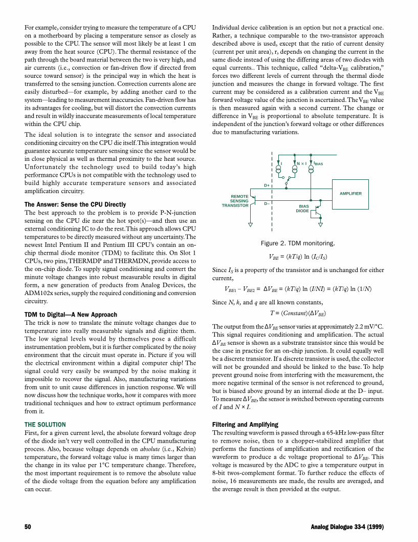
50 Analog Dialogue 33-4 (1999)
For example, consider trying to measure the temperature of a CPUon a motherboard by placing a temperature sensor as closely aspossible to the CPU. The sensor will most likely be at least 1 cmaway from the heat source (CPU). The thermal resistance of thepath through the board material between the two is very high, andair currents (i.e., convection or fan-driven flow if directed fromsource toward sensor) is the principal way in which the heat istransferred to the sensing junction. Convection currents alone areeasily disturbed—for example, by adding another card to thesystem—leading to measurement inaccuracies. Fan-driven flow hasits advantages for cooling, but will distort the convection currentsand result in wildly inaccurate measurements of local temperaturewithin the CPU chip.
The ideal solution is to integrate the sensor and associatedconditioning circuitry on the CPU die itself. This integration wouldguarantee accurate temperature sensing since the sensor would bein close physical as well as thermal proximity to the heat source.Unfortunately the technology used to build today’s highperformance CPUs is not compatible with the technology used tobuild highly accurate temperature sensors and associatedamplification circuitry.
The Answer: Sense the CPU DirectlyThe best approach to the problem is to provide P-N-junctionsensing on the CPU die near the hot spot(s)—and then use anexternal conditioning IC to do the rest. This approach allows CPUtemperatures to be directly measured without any uncertainty. Thenewest Intel Pentium II and Pentium III CPU’s contain an on-chip thermal diode monitor (TDM) to facilitate this. On Slot 1CPUs, two pins, THERMDP and THERMDN, provide access tothe on-chip diode. To supply signal conditioning and convert theminute voltage changes into robust measurable results in digitalform, a new generation of products from Analog Devices, theADM102x series, supply the required conditioning and conversioncircuitry.
TDM to Digital—A New ApproachThe trick is now to translate the minute voltage changes due totemperature into really measurable signals and digitize them.The low signal levels would by themselves pose a difficultinstrumentation problem, but it is further complicated by the noisyenvironment that the circuit must operate in. Picture if you willthe electrical environment within a digital computer chip! Thesignal could very easily be swamped by the noise making itimpossible to recover the signal. Also, manufacturing variationsfrom unit to unit cause differences in junction response. We willnow discuss how the technique works, how it compares with moretraditional techniques and how to extract optimum performancefrom it.
THE SOLUTIONFirst, for a given current level, the absolute forward voltage dropof the diode isn’t very well controlled in the CPU manufacturingprocess. Also, because voltage depends on absolute (i.e., Kelvin)temperature, the forward voltage value is many times larger thanthe change in its value per 1°C temperature change. Therefore,the most important requirement is to remove the absolute valueof the diode voltage from the equation before any amplificationcan occur.
Individual device calibration is an option but not a practical one.Rather, a technique comparable to the two-transistor approachdescribed above is used, except that the ratio of current density(current per unit area), r, depends on changing the current in thesame diode instead of using the differing areas of two diodes withequal currents.. This technique, called “delta-VBE calibration,”forces two different levels of current through the thermal diodejunction and measures the change in forward voltage. The firstcurrent may be considered as a calibration current and the VBE
forward voltage value of the junction is ascertained. The VBE valueis then measured again with a second current. The change ordifference in VBE is proportional to absolute temperature. It isindependent of the junction’s forward voltage or other differencesdue to manufacturing variations.
D+
D–BIAS
DIODE
I N 3 I IBIAS
REMOTESENSING
TRANSISTOR
AMPLIFIER
Figure 2. TDM monitoring.
VBE = (kT/q) ln (IC/IS)
Since IS is a property of the transistor and is unchanged for eithercurrent,
VBE1 – VBE2 = ∆VBE = (kT/q) ln (I/NI) = (kT/q) ln (1/N)
Since N, k, and q are all known constants,
T = (Constant)(∆VBE)
The output from the ∆VBE sensor varies at approximately 2.2 mV/°C.This signal requires conditioning and amplification. The actual∆VBE sensor is shown as a substrate transistor since this would bethe case in practice for an on-chip junction. It could equally wellbe a discrete transistor. If a discrete transistor is used, the collectorwill not be grounded and should be linked to the base. To helpprevent ground noise from interfering with the measurement, themore negative terminal of the sensor is not referenced to ground,but is biased above ground by an internal diode at the D– input.To measure ∆VBE, the sensor is switched between operating currentsof I and N × I.
Filtering and AmplifyingThe resulting waveform is passed through a 65-kHz low-pass filterto remove noise, then to a chopper-stabilized amplifier thatperforms the functions of amplification and rectification of thewaveform to produce a dc voltage proportional to ∆VBE. Thisvoltage is measured by the ADC to give a temperature output in8-bit twos-complement format. To further reduce the effects ofnoise, 16 measurements are made, the results are averaged, andthe average result is then provided at the output.

Analog Dialogue 33-4 (1999) 51
So how good is the TDM approach in practice?It is interesting to compare a TDM measurement with a moretraditional thermistor approach. The following example comparesresults obtained using a thermistor and a TDM channel to measurethe temperature of a 333-MHz Pentium II in a Slot 1 cartridge.The thermistor is in direct physical contact with the cartridgeheatsink. The TDM channel uses the on-chip diode and anADM1021 (with circuitry similar to those discussed above) toprovide the signal conditioning.
Besides being more accurate, it does not suffer from thermal lag.While contact with the heat sink is superior to earlier approacheswhere contact was not even made, it still exhibits majordisadvantages. As may be seen in Figure 4c the thermistor lagcompletely misses many of the thermal events due to its slowresponse time. Figure 4a shows a power up event while Figure 4bshows a power-down. Errors in excess of 20°C (representingcartridge temperature instead of actual chip temperature) areevident.
Even more significant is Figure 4c where the CPU is cycled in andout of Suspend mode. The thermistor completely misses these 20°Cthermal events. It’s easy to see how it would fail to protect a systemin the event of a rapid temperature rise due to a fault condition.All plots also demonstrate the offset error (due to packagetemperature drop) between the TDM and the thermistor as thetemperature increases. The offset can be taken care of by systemcalibration but there is nothing one can do to compensate forthermal lag. Indeed if additional system cooling were employed,the errors between the TDM and the thermistor would be greaterstill.
65
30
TE
MP
ER
AT
UR
E –
8C
60
55
50
40
35
45
TIME2:01 4:04 6:06 8:08 10:12 12:15
ADM1021 PLUS THERMAL DIODE
THERMISTOR
*POWER-UP MODE
Figure 4a. Start up.
65
TE
MP
ER
AT
UR
E –
8C
60
55
50
40
45
TIME0:0 0:31 1:03 1:35 2:06 2:38
ADM1021 PLUS THERMAL DIODE
THERMISTOR
*SUSPEND MODE
Figure 4b. Shut down.
70
TE
MP
ER
AT
UR
E –
8C
65
60
55
45
50
TIME0 0:12 0:25 0:38 0:52
ADM1021 PLUS THERMAL DIODE
THERMISTOR*SUSPEND/WAKE-UP
Figure 4c. Suspend/wake up cycling.
Using Discrete Transistors for TDMSo the TDM approach is very effective if the sensing diode isintegrated onto the die of the CPU whose temperature is beingmeasured. What about using this approach to measure temp-eratures where there isn’t an on-chip TDM, or to measure thetemperature of heat sources other than IC’s? The ∆VBE TDMapproach may also be used with stand-alone discrete transistors.Any NPN or PNP general-purpose transistor, such as 2N3904 or
D+
D–BIAS
DIODE
I N 3 I IBIAS
REMOTESENSING
TRANSISTOR LOWPASS FILTERfC = 65kHz
VDD
ADC
Figure 3. Signal conditioning.

52 Analog Dialogue 33-4 (1999)
2N3906, may be used as a remote sensor. With a discrete transistor,connect the base to the collector to form a 2-terminal device.Transistors are good temperature sensors since they have lowthermal mass and are easily mounted.
NPN
D+
D–
PNP
D+
D–
Figure 5. Transistor TDM.
If the transistor sensing junction is a significant distance away(>6 feet) and if it is used in noisy environments, the best methodto preserve signal integrity and prevent interference is to use twistedshielded cable. The maximum cable length is limited by cablecapacitance and by series resistance. Capacitance between D+ andD– causes settling time errors since the switched current needs tohave fully settled before the conversion is made.
VDD
STBY
SCLK
SDATA
ALERT
ADD0ADD1
GND
D+
D–
0.1mF ALL 10k V
3.3V
SET TO REQUIREDADDRESS
IN
OUT
I/O
SHIELD
2N3904
ADM1021
Figure 6. Transistor TDM plus ADM1021 for remote sensing.
TDM in Noisy EnvironmentsIt is very important to observe some guidelines when utilizingthermal diode sensing techniques, especially in noisy environments.The PC environment is inherently noisy and appears to be gettingnoisier as PCs get faster. As CPU speeds hurl towards 1 GHz,EMC noise becomes more of a headache. High speed graphicsports (AGP), high speed random-access memory, and high speeddisk access mean that there are many opportunities and paths fornoise to couple into sensitive analog circuitry. TDM is a verysensitive approach. The circuitry that drives the thermal diodeconsists of high-impedance, low-level current sources. To preventinterference, the TDM lines should be kept as short as possibleand shielded if there are high frequency noise sources in the vicinity.
Additional Features on the ADM1021In addition to the TDM channel, the ADM1021 includes an on-chip transistor for local or environmental temperature monitoring.A programmable conversion rate (from 1 conversion per 16 secondsup to 8 conversions per second) facilitates high update rates, whererapid temperature changes must be recorded. If fast updates arenot required, then lower update rates may be used to conservepower.
The ADM1021 also contains four limit registers to store localand remote, high and low temperature limits. A functional blockdiagram is shown in Figure 7. A typical system configuration usingthe ADM1021 is illustrated in Figure 8.
LOCAL TEMPERATURELOW LIMIT COMPARATOR
LOCAL TEMPERATUREHIGH LIMIT COMPARATOR
REMOTE TEMPERATURELOW LIMIT COMPARATOR
REMOTE TEMPERATUREHIGH LIMIT COMPARATOR
STATUS REGISTER
ADDRESS POINTERREGISTER
ONE-SHOTREGISTER
CONVERSION RATEREGISTER
LOCAL TEMPERATURELOW LIMIT REGISTER
REMOTE TEMPERATUREHIGH LIMIT REGISTER
CONFIGURATIONREGISTER
LOCAL TEMPERATUREHIGH LIMIT REGISTER
REMOTE TEMPERATURELOW LIMIT REGISTER
INTERRUPTMASKING
SMBUS INTERFACE
REMOTE TEMPERATUREVALUE REGISTER
LOCAL TEMPERATUREVALUE REGISTER
8-BIT A-TO-DCONVERTER
RUN/STANDBYBUSY
ON-CHIP TEMP.SENSOR
ANALOG MUX
TEST VDD NC GND GND NC NC TEST SDATA SCLK ADD0 ADD1
ALERT
STBY
D+
D–
ADM1021
EXTERNAL DIODE OPEN CIRCUIT
Figure 7. ADM1021 functional block diagram.

Analog Dialogue 33-4 (1999) 53
PROCESSOR
HOST BUS
BUILT-INSENSOR MAIN MEMORY
(DRAM)
SECOND LEVELCACHE
HOST-TO-PCIBRIDGE
MAIN MEMORY(DRAM)
PCI BUS (3.3V OR 5V 30/33MHz)
PCI SLOTS
AUDIO KEYBOARD BIOS
SDATASCLKALERT
D– D+
ADM1021
SERIAL PORTPARALLEL PORT
FLOPPY DISKCONTROLLER
INFRARED
USB PORT1
USB PORT2
GPI[I, O] (30+)
SMBUSISA/EIO BUS
(3.3V, 5V TOLERANT)
HARDDISKCD ROM
HARDDISK
BMI IDEULTRADMA/33
8237 1AB(PIIX4)
Figure 8. System architecture.
TDM CPU Monitoring Facilitates Optimum CoolingA thermal profile of a real-life notebook computer is illustrated inFigure 9. This shows how the temperature ramps up on the chipand in the computer environment once the monitoring utility startsrunning (after power-on and Windows boot). It is interesting tonote how hot both the CPU and the internal environment arerunning. The BIOS sets a CPU temperature limit of 92°C. Whenthis temperature is reached, the fan is switched on and remains onuntil the temperature drops below 82°C. Because both high andlow limits are programmed into the ADM1021, the fan can controlthe CPU temperature within a band between 82°C and 92°C. Thetemperature will oscillate between these two levels. If the fan fails,a higher temperature limit will shut the system down if it isbreached. It is also interesting to note that the environmenttemperature also reaches very high temperatures, approximately10°C below the CPU temperature, within a notebook housing.
This example illustrates the importance of TDM techniques inCPU temperature management. Prior to this technique, it wouldhave been impossible to extract such high performance levels fromthe CPU without overheating—or unduly wasting battery life bycontinuously cooling the system. b
100
30
TE
MP
ER
AT
UR
E –
8C
90
80
70
50
40
60
TIME
CPU
CONTROLLING
RAMP UP
REMOTE TEMPERATURE
LOCAL TEMPERATURE
Figure 9. Temperature profile from a typical notebookcomputer.
AUDIO (ANALOG & DIGITAL)AC ’97 SoundMAX® Audio Codec
The AD1881 audio codec is used to add audio capabilities tocomputer motherboards when directly connected to the Intel®
82440MX Mobile Chipset or the Desk Top 82801 I/O controllerhub (ICH). This direct connection capability makes use of existingsystem resources, adding flexibility, improving sound quality(including Phat™ 3-D stereo enhancement), and lowering systemparts costs by eliminating components. The AD1881 was developedand validated to the Intel Audio Codec ’97 (AC ’97) 2.1
Component Specification. Systems designated as SoundMAX®,an Analog Devices registered trademark, include an audio codec,amplifiers and driver software, and several specific features fornotebook and commercial desktop PCs. Specific features includevariable sample-rate capability (7 kHz to 48 kHz 6 1 Hz), mixermodes, true line-level output, multibit sigma-delta architecturefor SNRs > 90 dB, 16-bit stereo full-duplex, capabilities for Line,CD, Video, and Aux (stereo), plus speakerphone, PC Beep, andMic (32) (mono). The AD1881, housed in a 48-lead LQFP, isspecified for 5 V supplies (3.3-V digital) and 0 to 70° C temperaturerange. Price (1000s) is $4.64.
New-Product Brief

54 Analog Dialogue 33-9 (1999)
Compensate forLoading Effects onPower Lines with aDSP-Controlled ActiveShunt FilterMichal Gwozdz, Ph.D. Eng.,Analog Devices DSP Field Applications Engineer,P.E.P. ALFINERyszard Porada, Ph.D. Eng.Poznan University of Technology
INTRODUCTIONSystems with passive LC elements, such as capacity compensators,resonant passive filters of higher harmonics, or filters withstructures and parameters determined by optimization methodshave been traditionally used to compensate for power factor andother loading effects imposed by electricity users on the powernetwork. However, widespread use of loads that involve power-electronic systems can cause major distortion of voltage and(especially) current waveforms, and even cause substantial dccurrents to flow in power transformer secondaries. For these typesof loads, the kinds of compensation systems mentioned above oftenprove to be unsatisfactory. Nowadays, power-system engineers aremore likely to consider using other types of compensators,especially active power filters or hybrid systems (power filters withpassive L-C elements such as those described in References 2, 3,6, 7, 8, 9, 11) to increase system efficiency.
Recent approaches to development of compensation methods aimto develop compensators of a type that would be able to realizedynamic compensation (in real time) and would also be moreresistant to interference caused by the power network or electricityusers. Their objectives include optimization of the loads as seenby power sources (power network). According to Fryze’s suggestion[5] and subsequent developments [4, 10, 12, 13], to achieve suchcompensation it is necessary to eliminate a differential current(between a distorted load current and an ideal form of current(i.e., in-phase sine wave)) flowing through the power source. Inconcept, this can be done by generating and injecting a currentequal to and in opposite phase to the differential current. Inpractice, obtaining such a source is difficult; what is really calledfor is an active system with parametric elements or controlled-current power sources.
STRUCTURE OF AN ACTIVE FILTERIn this article we consider a proposal to employ a power-electroniccurrent source controlled through the use of digital-signal-processing computer technology to achieve an active shunt filter(alternative names are: differential current compensation system orcompensator), to approach a realization of optimal compensation.The assumed aim is dynamic compensation of differential cur-rent, which is the difference between load current iL (t) and referencecurrent iREF (t). The reference current is the optimal active cur-rent calculated with the method suggested in article [10]. Figure1 shows the block diagram of the system.
FK
DM–
+ idIM
iREF
CM PI
iFK
EM
iINV
CT
LINV
CT
VT
ACTIVE FILTER
uL
LOA
D
iL
us
PO
WE
R S
OU
RC
E
is
Figure 1. Block diagram of the active filter.
The active filter consists of the following modules and elements:• Control Module (CM), based on a microcomputer system with
digital signal processing (DSP),
• Execution Module (EM) in form of a power-electronic currentsource,
• Voltage (VT) and current (CT) transducers [Types LA55-P andLV25 (LEM®)].
The active filter control process occurs in two phases:• Determining the reference current
i tREF ( ) ,
• Dynamic shaping of desired compensator current in the form
i t i t i tINV L REF( ) = ( ) − ( )
The quality and dynamic properties of the compensation processdepend mostly on the method used for calculating the reference-current parameters. Akagi et al’s theory of instantaneous reactivepower [1] is commonly used to control power active filters. Theauthors believe that this theory does not fulfill the requirementsof optimization of work in an energy source/receiver system. Thegeneral aim of optimization is to minimize the out-of-phasecomponent of source current, reduce distortion of sinusoidalwaveforms, and minimize active power losses in transmission ofenergy from source to receiver. To determine a current which wouldhave such properties, we applied the variational methods of [10].As a result, we obtained an expression describing an optimal sourcecurrent (the target reference current) in the following analytical form:
i t i t k t G t e t A t e tREF a e e REF( ) = ( ) = ( ) ( ) ( ) = ( ) ( )
Where: e (t) is the voltage source, eG(t) the equivalent conductancein form: eG(t) = aP(t)/E2(t), where: aP(t) and E(t) are instantaneousvalues of active power and rms voltage source [10]. The frequencyand phase of the reference signal correspond to suitable values ofthe first harmonic of the voltage source, e(t).
To effectively realize the whole control process, CM was dividedinto two sub-modules:• the Identification Module (IM), which calculates frequency,
wREF, phase, ϕREF, and amplitude, AREF, of reference current,iREF(t),
• the Decision Module (DM), which performs these tasks:- shaping magnitude and phase characteristics of the active filter
to obtain wideband transfer and high open-loop gain in thefeedback loop. This is necessary to ensure a high degree ofcompensation of non-linear current and to work stably underconditions of a wide variety of load parameters,
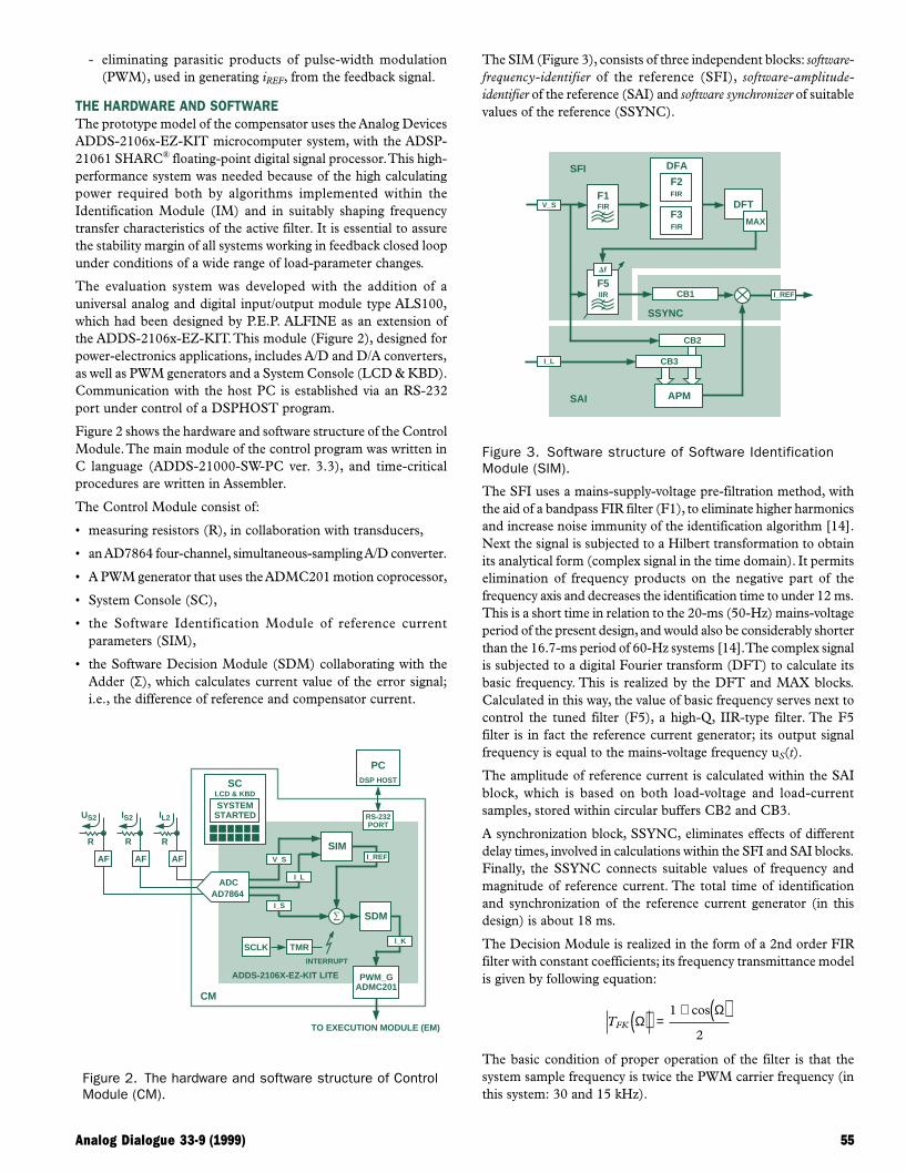
Analog Dialogue 33-9 (1999) 55
- eliminating parasitic products of pulse-width modulation(PWM), used in generating iREF, from the feedback signal.
THE HARDWARE AND SOFTWAREThe prototype model of the compensator uses the Analog DevicesADDS-2106x-EZ-KIT microcomputer system, with the ADSP-21061 SHARC® floating-point digital signal processor. This high-performance system was needed because of the high calculatingpower required both by algorithms implemented within theIdentification Module (IM) and in suitably shaping frequencytransfer characteristics of the active filter. It is essential to assurethe stability margin of all systems working in feedback closed loopunder conditions of a wide range of load-parameter changes.
The evaluation system was developed with the addition of auniversal analog and digital input/output module type ALS100,which had been designed by P.E.P. ALFINE as an extension ofthe ADDS-2106x-EZ-KIT. This module (Figure 2), designed forpower-electronics applications, includes A/D and D/A converters,as well as PWM generators and a System Console (LCD & KBD).Communication with the host PC is established via an RS-232port under control of a DSPHOST program.
Figure 2 shows the hardware and software structure of the ControlModule. The main module of the control program was written inC language (ADDS-21000-SW-PC ver. 3.3), and time-criticalprocedures are written in Assembler.
The Control Module consist of:
• measuring resistors (R), in collaboration with transducers,
• an AD7864 four-channel, simultaneous-sampling A/D converter.
• A PWM generator that uses the ADMC201 motion coprocessor,
• System Console (SC),
• the Software Identification Module of reference currentparameters (SIM),
• the Software Decision Module (SDM) collaborating with theAdder (Σ), which calculates current value of the error signal;i.e., the difference of reference and compensator current.
SIM
SDM
PWM_GADMC201
SCLK TMR
INTERRUPT
I_REF
I_L
V_S
I_S
I_K
ADDS-2106X-EZ-KIT LITE
RS-232PORT
PCDSP HOSTSC
LCD & KBD
CM
TO EXECUTION MODULE (EM)
AFAF AF
IL2IS2US2
RRR
ADCAD7864
SYSTEMSTARTED
Figure 2. The hardware and software structure of ControlModule (CM).
The SIM (Figure 3), consists of three independent blocks: software-frequency-identifier of the reference (SFI), software-amplitude-identifier of the reference (SAI) and software synchronizer of suitablevalues of the reference (SSYNC).
APM
CB3
CB2
SAI
I_L
CB1
SSYNC
I_REFF5
DFT
MAX
DFA
F2
F3
SFI
V_S
IIR
Df
FIR
FIR
F1FIR
Figure 3. Software structure of Software IdentificationModule (SIM).
The SFI uses a mains-supply-voltage pre-filtration method, withthe aid of a bandpass FIR filter (F1), to eliminate higher harmonicsand increase noise immunity of the identification algorithm [14].Next the signal is subjected to a Hilbert transformation to obtainits analytical form (complex signal in the time domain). It permitselimination of frequency products on the negative part of thefrequency axis and decreases the identification time to under 12 ms.This is a short time in relation to the 20-ms (50-Hz) mains-voltageperiod of the present design, and would also be considerably shorterthan the 16.7-ms period of 60-Hz systems [14]. The complex signalis subjected to a digital Fourier transform (DFT) to calculate itsbasic frequency. This is realized by the DFT and MAX blocks.Calculated in this way, the value of basic frequency serves next tocontrol the tuned filter (F5), a high-Q, IIR-type filter. The F5filter is in fact the reference current generator; its output signalfrequency is equal to the mains-voltage frequency uS(t).
The amplitude of reference current is calculated within the SAIblock, which is based on both load-voltage and load-currentsamples, stored within circular buffers CB2 and CB3.
A synchronization block, SSYNC, eliminates effects of differentdelay times, involved in calculations within the SFI and SAI blocks.Finally, the SSYNC connects suitable values of frequency andmagnitude of reference current. The total time of identificationand synchronization of the reference current generator (in thisdesign) is about 18 ms.
The Decision Module is realized in the form of a 2nd order FIRfilter with constant coefficients; its frequency transmittance modelis given by following equation:
TFK Ω
Ω( ) =+ ( )1
2
cos
The basic condition of proper operation of the filter is that thesystem sample frequency is twice the PWM carrier frequency (inthis system: 30 and 15 kHz).

56 Analog Dialogue 33-9 (1999)
The Execution Module is a power-electronics controlled currentsource, which uses a highly integrated Intelligent Power Module(IPM) type PM50RSA120 (Mitsubishi) and inductance coil, LINV.This coil also limits parasitic products of the PWM.
The general source of energy for the current source is a capacitorwithin the dc circuit of the inverter (IPM). The inverter is coupledwith the Control Module with the aid of fast photocouplers.
PERFORMANCE OF THE PROTOTYPE SYSTEMExperimental tests of the above-mentioned prototype models ofthe power-electronic current source and single-phase activecompensation system were carried out for different types of loadand supply conditions. Here is a small selection of the results ofthe tests.
The waveforms of Figure 4 show the rectangular shape of referencesignal iREF(t), output current of current source iS(t) and feedbacksignal iFK(t) (Figure 4a), and results of spectrum analysis of thesequantities (Figure 4b). The bandwidth (–3 dB) of the currentsource was equal to 3.2 kHz with non-uniform amplitudecharacteristic 0.4 dB. The total harmonic distortion (THD) ofoutput current within this band was 0.7%—and 0.2% within the0.5-kHz bandwidth.
a) Waveforms of selected quantities.
Fi REF
S
20
10
1
0.1
0.01
0.001
[A]
FREQUENCY – Hz
0 50 150 500 1000
Fi
b) Spectrum analysis.
Figure 4. Investigation results of current source prototypesystem for the case of rectangular shape of reference signal.
Figures 5 and 6 illustrate the workings of the complete active filter.The source of the distorted current (Figure 5) is a simple single-diode rectifier with an R-L-type load (resistor and inductor inseries). It is a particularly unfavorable case, because itsimultaneously generates a strongly distorted current with a dccomponent and reactive power. The waveforms of source voltage,uS, and currents of load, iL, power network, iS, active filter, iINV
and reference signal iREF, are shown in Figure 5a—and also resultsof spectrum analysis of selected quantities (Figure 5b). Figure 6shows similar quantities for an RC-loaded 4-diode-bridge, thetypical configuration of most consumer-electronics power packs.
a) Waveforms of selected voltage and current quantities.
b) Spectrum analysis.
Figure 5. Investigation results of the active-filter prototypemodel with a strongly nonlinear passive receiver—a single-diode rectifier with an R-L (resistance and inductance inseries) load.
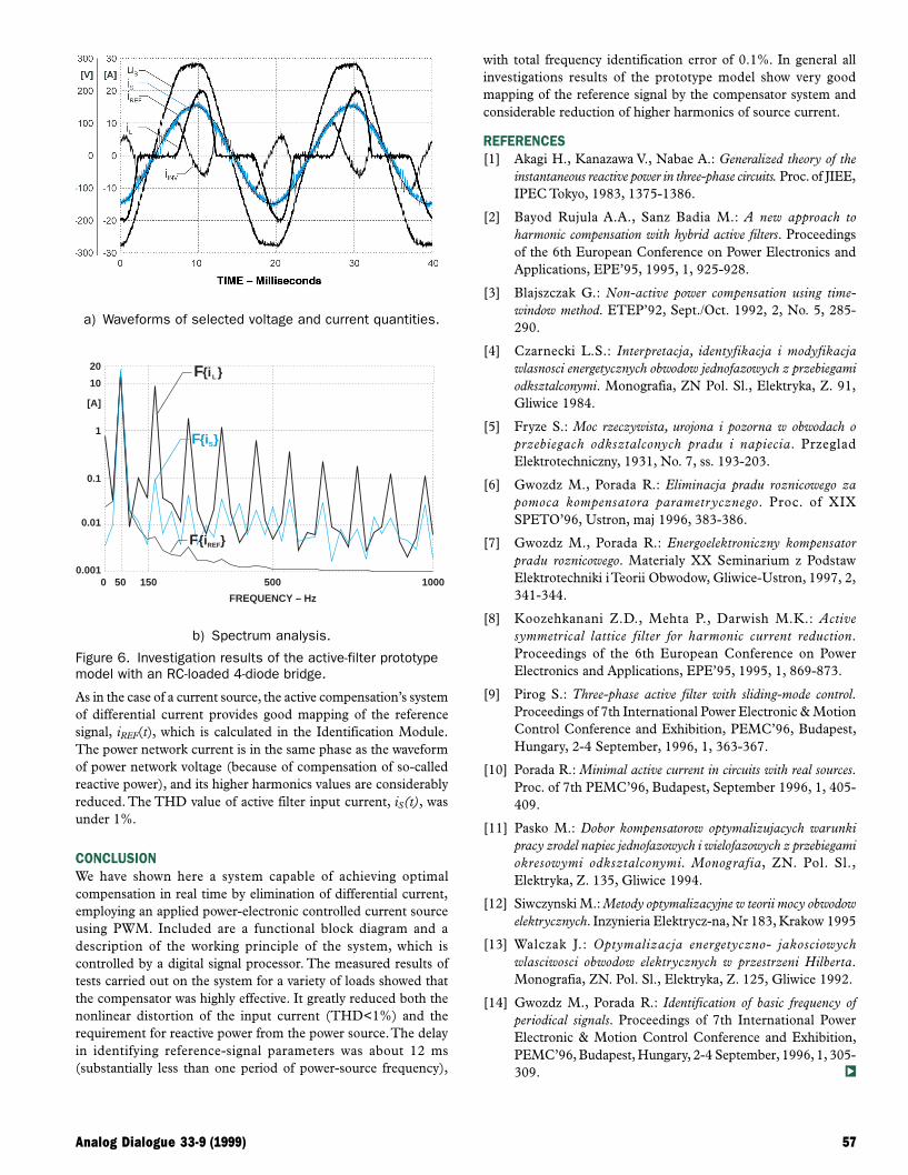
Analog Dialogue 33-9 (1999) 57
a) Waveforms of selected voltage and current quantities.
Fi S
F
Fi L20
10
1
0.1
0.01
0.001
[A]
FREQUENCY – Hz
0 50 150 500 1000
F REi
b) Spectrum analysis.
Figure 6. Investigation results of the active-filter prototypemodel with an RC-loaded 4-diode bridge.
As in the case of a current source, the active compensation’s systemof differential current provides good mapping of the referencesignal, iREF(t), which is calculated in the Identification Module.The power network current is in the same phase as the waveformof power network voltage (because of compensation of so-calledreactive power), and its higher harmonics values are considerablyreduced. The THD value of active filter input current, iS(t), wasunder 1%.
CONCLUSIONWe have shown here a system capable of achieving optimalcompensation in real time by elimination of differential current,employing an applied power-electronic controlled current sourceusing PWM. Included are a functional block diagram and adescription of the working principle of the system, which iscontrolled by a digital signal processor. The measured results oftests carried out on the system for a variety of loads showed thatthe compensator was highly effective. It greatly reduced both thenonlinear distortion of the input current (THD<1%) and therequirement for reactive power from the power source. The delayin identifying reference-signal parameters was about 12 ms(substantially less than one period of power-source frequency),
with total frequency identification error of 0.1%. In general allinvestigations results of the prototype model show very goodmapping of the reference signal by the compensator system andconsiderable reduction of higher harmonics of source current.
REFERENCES[1] Akagi H., Kanazawa V., Nabae A.: Generalized theory of the
instantaneous reactive power in three-phase circuits. Proc. of JIEE,IPEC Tokyo, 1983, 1375-1386.
[2] Bayod Rujula A.A., Sanz Badia M.: A new approach toharmonic compensation with hybrid active filters. Proceedingsof the 6th European Conference on Power Electronics andApplications, EPE’95, 1995, 1, 925-928.
[3] Blajszczak G.: Non-active power compensation using time-window method. ETEP’92, Sept./Oct. 1992, 2, No. 5, 285-290.
[4] Czarnecki L.S.: Interpretacja, identyfikacja i modyfikacjawlasnosci energetycznych obwodow jednofazowych z przebiegamiodksztalconymi. Monografia, ZN Pol. Sl., Elektryka, Z. 91,Gliwice 1984.
[5] Fryze S.: Moc rzeczywista, urojona i pozorna w obwodach oprzebiegach odksztalconych pradu i napiecia. PrzegladElektrotechniczny, 1931, No. 7, ss. 193-203.
[6] Gwozdz M., Porada R.: Eliminacja pradu roznicowego zapomoca kompensatora parametr ycznego. Proc. of XIXSPETO’96, Ustron, maj 1996, 383-386.
[7] Gwozdz M., Porada R.: Energoelektroniczny kompensatorpradu roznicowego. Materialy XX Seminarium z PodstawElektrotechniki i Teorii Obwodow, Gliwice-Ustron, 1997, 2,341-344.
[8] Koozehkanani Z.D., Mehta P., Darwish M.K.: Activesymmetrical lattice filter for harmonic current reduction.Proceedings of the 6th European Conference on PowerElectronics and Applications, EPE’95, 1995, 1, 869-873.
[9] Pirog S.: Three-phase active filter with sliding-mode control.Proceedings of 7th International Power Electronic & MotionControl Conference and Exhibition, PEMC’96, Budapest,Hungary, 2-4 September, 1996, 1, 363-367.
[10] Porada R.: Minimal active current in circuits with real sources.Proc. of 7th PEMC’96, Budapest, September 1996, 1, 405-409.
[11] Pasko M.: Dobor kompensatorow optymalizujacych warunkipracy zrodel napiec jednofazowych i wielofazowych z przebiegamiokresowymi odksztalconymi. Monografia, ZN. Pol. Sl.,Elektryka, Z. 135, Gliwice 1994.
[12] Siwczynski M.: Metody optymalizacyjne w teorii mocy obwodowelektrycznych. Inzynieria Elektrycz-na, Nr 183, Krakow 1995
[13] Walczak J.: Optymalizacja energetyczno- jakosciowychwlasciwosci obwodow elektrycznych w przestrzeni Hilberta.Monografia, ZN. Pol. Sl., Elektryka, Z. 125, Gliwice 1992.
[14] Gwozdz M., Porada R.: Identification of basic frequency ofperiodical signals. Proceedings of 7th International PowerElectronic & Motion Control Conference and Exhibition,PEMC’96, Budapest, Hungary, 2-4 September, 1996, 1, 305-309. b

58 Analog Dialogue 33-2 (1999)
Ask the Applications Engineer—27By Bill Englemann
SIGNAL CORRUPTION IN INDUSTRIAL MEASUREMENTQ. What problems am I most likely to run into when instrumenting an
industrial system?
A. The five kinds of problems most frequently reported bycustomers of our I/O Subsystems (IOS) Division are:
1. GROUND LOOPSGround loops are the bane of instrumentation engineers andtechnicians. They cause many lost hours troubleshootingobscure and hard-to-diagnose measurement problems. Dothese symptoms sound familiar?
• Readings slowly drift even though you know the sensor isnot changing.
• Readings shift when another piece of equipment is turned on.
• Measurements differ when a calibration device is connectedat the end of an instrument cable instead of directly at the input.
• A 60-Hz sine wave is superimposed upon your dcmeasurement input.
• There are unexplained measurement equipment failures.
Any of these problems can be caused by ground loops—inadvertent flows of current through “ground,” “common” and“reference” paths connected to points at nominally the samepotential. And all of these problems can be eliminated byisolation, the key signal-conditioning attribute we offer in allour signal conditioning series.
Sometimes separate grounding of two pieces of equipmentintroduces a potential difference and causes current to flowthrough signal lines. Why would this happen if they were bothgrounded? Because the earth and metal structures are actuallyrelatively poor conductors of electricity when compared withthe copper wires that carry power and signals. This inherentresistance to current flow varies with the weather and time ofyear and causes current to flow through any wires that areconnecting the two devices. Many factory and plant buildingsexperience potentials of several tens or hundreds of volts.Appropriate signal conditioning eliminates the possibility ofground loops by electrically isolating the equipment. Signalconditioning will also protect equipment, rejecting potentiallydamaging voltage levels before entering the sensitivemeasurement system.
Isolation provides a completely floating input and output port,where there is no electrical path from field input to output andto power. Hence, there is no path for current to flow, and nopossibility of ground loops.
Q. How is this possible? How can we provide a path for the signal frominput to output, without any path for current to flow?
A. It’s done by magnetic isolation. A representation of the signalis passed through a transformer, which creates a magnetic—not a galvanic—connection. We have perfected the use oftransformers for accurate, reliable low-level signal isolation.This approach employs a modulator and demodulator totransmit the signal across the transformer barrier, and canachieve isolation levels of 2500 volts ac.
One of the most frequently encountered application problemsinvolves measuring a low-level sensor such as a thermocouplein the presence of as much as hundreds of volts of groundpotential. This potential is known as common-mode voltage. Theability of a high-quality signal conditioner to reject errorscaused by common-mode voltage, while still accuratelyamplifying low-level signals is known as common mode rejection(CMR). Our 5B, 6B and 7B Series signal conditioningsubsystems provide sufficient common-mode rejection toreduce the impact of these errors by a factor of 100 million to 1!
2. MISWIRING AND OVERVOLTAGEYou know what happens when a cable from a sensitive dataacquisition board is routed into another cabinet, or anotherpart of the building—the input and output wiring terminalsare grouped among hundreds of other terminals carryingdiverse signals and levels: dc signals, ac signals, milli-voltage,thermocouples, dc power, ac power, proximity switches, relaycircuits, etc. It’s not difficult to imagine even a well trainedtechnician or electrician connecting a wire to the wrongterminal. Wiring diagrams are often updated in real time witha red pen, as system needs change. Equipment gets replacedwith “equivalents.” Sometimes power supplies fail and excessvoltages are applied inadvertently. What can you do to protectyour measurement system?
The answer lies in using rugged signal conditioning onevery analog signal lead. This inexpensive insurance policyprovides protection against miswiring and overvoltage on eachinput and output signal line. For example, the use of a5B Series signal conditioner will provide 240 -V ac of protection,even on input lines used to measure sensitive thermocouplesignals, with levels in the millivolt range. You can literallyconnect a 240-V ac line across the same input lines usedto measure the thermocouple, without any damage. The useof signal conditioning to interface with field I/O will protectall measurement and data acquisition equipment on thesystem side.
3. LOSS OF RESOLUTIONResolution is the smallest change in the measurement that theanalog-digital converter (ADC) system can detect and respondto. For example, if a temperature reading steps from 100.00°to 100.29° to 100.58°, as the actual temperature graduallyincreases through this range, the resolution (least-significant-bit value) is 0.29°. This would occur if you had a signalconditioner measuring a thermocouple with a range of 0° to+1200° and a 12-bit ADC. There are two ways to improve this(make the resolution smaller) and detect smaller changes - usea higher resolution ADC or use a smaller measurement range.
For example, a 15-bit plus sign ADC of the type used in our6B Series would offer resolution of 0.037° on the 0 to 1200°range example, 8 times smaller! On the other hand, if you knewthat most of the time the temperature would be in the vicinityof 100°, you could order from Analog Devices a thermocouplesignal conditioner with a custom range, calibrated for the exactthermocouple type and temperature measurement range. Forexample, a custom-ranged signal conditioner with a span of+50° to +150° would offer resolution of 0.024° with a 12-bitADC, a big improvement over the 0 to 1200° range.
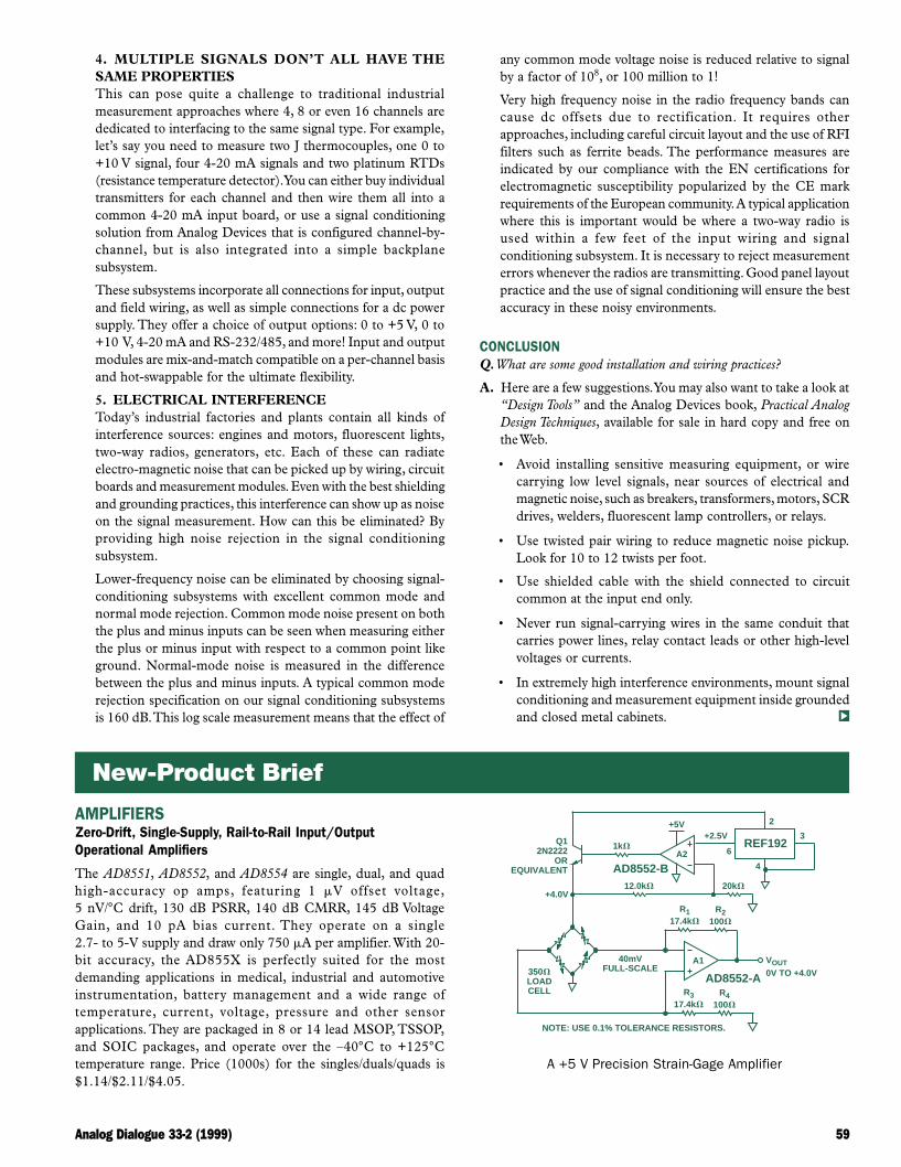
Analog Dialogue 33-2 (1999) 59
4. MULTIPLE SIGNALS DON’T ALL HAVE THESAME PROPERTIESThis can pose quite a challenge to traditional industrialmeasurement approaches where 4, 8 or even 16 channels arededicated to interfacing to the same signal type. For example,let’s say you need to measure two J thermocouples, one 0 to+10 V signal, four 4-20 mA signals and two platinum RTDs(resistance temperature detector). You can either buy individualtransmitters for each channel and then wire them all into acommon 4-20 mA input board, or use a signal conditioningsolution from Analog Devices that is configured channel-by-channel, but is also integrated into a simple backplanesubsystem.
These subsystems incorporate all connections for input, outputand field wiring, as well as simple connections for a dc powersupply. They offer a choice of output options: 0 to +5 V, 0 to+10 V, 4-20 mA and RS-232/485, and more! Input and outputmodules are mix-and-match compatible on a per-channel basisand hot-swappable for the ultimate flexibility.
5. ELECTRICAL INTERFERENCEToday’s industrial factories and plants contain all kinds ofinterference sources: engines and motors, fluorescent lights,two-way radios, generators, etc. Each of these can radiateelectro-magnetic noise that can be picked up by wiring, circuitboards and measurement modules. Even with the best shieldingand grounding practices, this interference can show up as noiseon the signal measurement. How can this be eliminated? Byproviding high noise rejection in the signal conditioningsubsystem.
Lower-frequency noise can be eliminated by choosing signal-conditioning subsystems with excellent common mode andnormal mode rejection. Common mode noise present on boththe plus and minus inputs can be seen when measuring eitherthe plus or minus input with respect to a common point likeground. Normal-mode noise is measured in the differencebetween the plus and minus inputs. A typical common moderejection specification on our signal conditioning subsystemsis 160 dB. This log scale measurement means that the effect of
any common mode voltage noise is reduced relative to signalby a factor of 108, or 100 million to 1!
Very high frequency noise in the radio frequency bands cancause dc offsets due to rectification. It requires otherapproaches, including careful circuit layout and the use of RFIfilters such as ferrite beads. The performance measures areindicated by our compliance with the EN certifications forelectromagnetic susceptibility popularized by the CE markrequirements of the European community. A typical applicationwhere this is important would be where a two-way radio isused within a few feet of the input wiring and signalconditioning subsystem. It is necessary to reject measurementerrors whenever the radios are transmitting. Good panel layoutpractice and the use of signal conditioning will ensure the bestaccuracy in these noisy environments.
CONCLUSIONQ. What are some good installation and wiring practices?
A. Here are a few suggestions. You may also want to take a look at“Design Tools” and the Analog Devices book, Practical AnalogDesign Techniques, available for sale in hard copy and free onthe Web.
• Avoid installing sensitive measuring equipment, or wirecarrying low level signals, near sources of electrical andmagnetic noise, such as breakers, transformers, motors, SCRdrives, welders, fluorescent lamp controllers, or relays.
• Use twisted pair wiring to reduce magnetic noise pickup.Look for 10 to 12 twists per foot.
• Use shielded cable with the shield connected to circuitcommon at the input end only.
• Never run signal-carrying wires in the same conduit thatcarries power lines, relay contact leads or other high-levelvoltages or currents.
• In extremely high interference environments, mount signalconditioning and measurement equipment inside groundedand closed metal cabinets. b
AMPLIFIERSZero-Drift, Single-Supply, Rail-to-Rail Input/OutputOperational Amplifiers
The AD8551, AD8552, and AD8554 are single, dual, and quadhigh-accuracy op amps, featuring 1 mV offset voltage,5 nV/°C drift, 130 dB PSRR, 140 dB CMRR, 145 dB VoltageGain, and 10 pA bias current. They operate on a single2.7- to 5-V supply and draw only 750 mA per amplifier. With 20-bit accuracy, the AD855X is perfectly suited for the mostdemanding applications in medical, industrial and automotiveinstrumentation, battery management and a wide range oftemperature, current, voltage, pressure and other sensorapplications. They are packaged in 8 or 14 lead MSOP, TSSOP,and SOIC packages, and operate over the –40°C to +125°Ctemperature range. Price (1000s) for the singles/duals/quads is$1.14/$2.11/$4.05.
New-Product Brief
VOUT350VLOADCELL
AD8552-A
R117.4kV
R2100V
0V TO +4.0V
NOTE: USE 0.1% TOLERANCE RESISTORS.
20kV
A1
A2
AD8552-B
REF192
12.0kV
1kV
+5V+2.5V
6
4
3
2
+4.0V
40mVFULL-SCALE
Q12N2222
OREQUIVALENT
R317.4kV
R4100V
A +5 V Precision Strain-Gage Amplifier
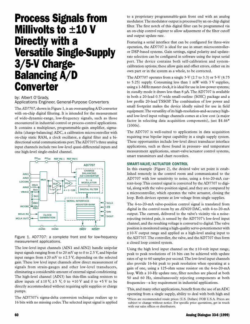
60 Analog Dialogue 33-6 (1999)
Process Signals fromMillivolts to 610 VDirectly with aVersatile Single-Supply3/5-V Charge-Balancing A/DConverterby: Albert O’Grady,Applications Engineer, General-Purpose Converters
The AD7707, shown in Figure 1, is an oversampling A/D converterwith on-chip digital filtering. It is intended for the measurementof wide-dynamic-range, low-frequency signals, such as thoseencountered in industrial control or process-control applications.It contains a multiplexer, programmable-gain amplifier, sigma-delta (charge-balancing) ADC, a calibration microcontroller withon-chip static RAM, a clock oscillator, a digital filter and a bi-directional serial communications port. The AD7707’s three analoginput channels include two low-level quasi-differential inputs andone high-level single-ended channel.
AVDD REF IN(–) REF IN(+)
AD7707
MUX
PGA
CHARGEBALANCING
A/D CONVERTER
S – DMODULATOR
DIGITAL FILTERA = 1<128
SERIAL INTERFACE
REGISTER BANK
CLOCKGENERATIONMCLK OUT
MCLK IN
AGND DRDY RESET
BUF
AIN1
AIN2
LOCOM
AIN3
VBIAS
HICOM
DIN
DOUT
CS
SCLK
DGND
30kV
5kV
15kV
30kV
5kV
DVDD
Figure 1. AD7707: a complete front end for low-frequencymeasurement applications.
The low-level input channels (AIN1 and AIN2) handle unipolarinput signals ranging from 0 to 20 mV up to 0 to 2.5 V, and bipolarinput ranges from ±20 mV to ±2.5 V, depending on the selectedgain. These low level input channels allow direct measurement ofsignals from strain-gauges and other low-level transducers,eliminating a considerable amount of external signal conditioning.The high-level channel (AIN3) has thin-film scaling resistors toallow inputs of ±10 V, ±5 V, 0 to +10 V and 0 to +5 V to bedirectly accommodated without requiring split supplies or chargepumps.
The AD7707’s sigma-delta conversion technique realizes up to16 bits with no missing codes. The selected input signal is applied
to a proprietary programmable-gain front end with an analogmodulator. The modulator output is processed by an on-chip digitalfilter. The first notch of this digital filter can be programmed viaan on-chip control register to allow adjustment of the filter cutoffand output update rate.
Featuring a serial interface that can be configured for three-wireoperation, the AD7707 is ideal for use in smart microcontroller-or DSP-based systems. Gain settings, signal polarity and update-rate selection can be configured in software using the input serialport. The device contains both self-calibration and system-calibration options; these allow gain and offset errors, either on itsown part or in the system as a whole, to be corrected.
The AD7707 operates from a single 3-V (2.7 to 3.3) or 5-V (4.75to 5.25) supply. Consuming less than 1 mW with 3 V supplies,using a 1-MHz master clock, it is ideal for use in low-power systems;in standby mode it draws less than 8 µA. The AD7707 is availablein both a 20-lead 0.3"-wide small-outline (SOIC) package and alow profile 20-lead TSSOP. The combination of low power andsmall footprint makes the device ideally suited for use in fieldequipment. The versatility of its high-resolution-and-accuracy high-and low-level input voltage channels comes at a low cost (a majorfactor in selecting data acquisition components), just $4.46*(1000s).
The AD7707 is well-suited to applications in data acquisitionrequiring true bipolar input capability in a single supply system.These opportunities include low-level direct transducer interfaceapplications, such as those found in pressure- and temperaturemeasurement applications, smart-valve/actuator control systems,smart transmitters and chart recorders.
SMART-VALVE/ACTUATOR CONTROLIn this example (Figure 2), the desired valve set point is estab-lished remotely in the control room and communicated to theAD7707 with low sensitivity to noise, using a 4-to-20-mA cur-rent-loop. This control signal is converted by the AD7707 to digi-tal, along with the valve-position signal, and they are compared bya microcontroller, which operates the valve actuator, closing theloop. Both devices operate at low voltage from single supplies.
The 4-to-20-mA valve-position control signal is translated fromdigital in the control room by an AD420 DAC, with 4-to-20-mAoutput. The current, delivered to the valve’s vicinity via a noise-rejecting twisted pair, is sensed by the AD7707’s low-level inputchannel, and the resulting voltage is converted to digital. The valveposition is monitored using a high-quality servo-potentiometer with±10-V output range and applied as a high-level analog input tothe AD7707. The controller, the valve, and the AD7707 thus forma closed loop control system.
Using the high level input channel on the ±10-volt input range,peak to peak resolutions of 16 bits can be achieved with updaterates of up to 60 samples per second. The low-level input channelsalso provide 16-bit peak to peak resolution when operating at again of one, using a 125-ohm sense resistor on the 4-to-20-mAloop. With a 10-Hz update rate, filter notches are placed at both50 and 60 Hz, simultaneously rejecting components at bothfrequencies—a key requirement in industrial applications.
This, and many other applications, benefit from the use of an ADCoperating from a single supply, ability to deal with both high and*Prices are recommended resale prices (U.S. Dollars) FOB U.S.A. Prices aresubject to change without notice. For specific price quotations, get in touchwith our sales offices or distributors.
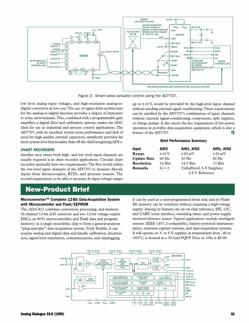
Analog Dialogue 33-6 (1999) 61
low level analog input voltages, and high-resolution analog-to-digital conversion at low cost. The use of sigma-delta architecturefor the analog-to-digital function provides a degree of immunityto noisy environments. This, combined with a programmable gainamplifier, a digital filter and calibration options, makes the ADCideal for use in industrial and process control applications. TheAD7707, with its excellent system noise performance and lack ofneed for high-quality external capacitors, manifestly provides farmore system level functionality than off-the-shelf integrating ADCs.
CHART RECORDERSAnother area where both high- and low level input channels areusually required is in chart recorder applications. Circular chartrecorders generally have two requirements. The first would utilizethe low-level input channels of the AD7707 to measure directlyinputs from thermocouples, RTDs, and pressure sensors. Thesecond requirement, to be able to measure dc input voltage ranges
Figure 2. Smart-valve/actuator control using the AD7707.
AD7707
DVDD
+5V
AIN2
REF IN(–)
AGND
MCLK IN
MCLK OUTREF IN(+)
AVDD
AIN1
LOCOM
2.5V
AIN3
VBIAS
HICOM
DGND
MICRO-CONTROLLER
ACTUATOR/VALVE
610V
SMARTVALVE/ACTUATOR
RSENSE
SCLK
DOUT
DIN
PO
SCLK
DIN
DOUT
CSSTANDARDSPI INTERFACEBETWEENMICROCONTROLLERAND AD7707
THE MICROCONTROLLER CONTROLS THE VALVE/ACTUATOR
AD7707 MONITORSOUTPUT FROM ASERVO-POTENTIOMETERWHERE OUTPUT RANGEIS –10V TO +10V
5
2
4
6
7
8
9
C1 C2
VCC = 24V
20 21 23
VLL
IOUT (4mA–20mA)
REFOUT
REFIN
1514 11
GND
RANGESELECT 1
RANGESELECT 2CLEAR
LATCH
CLOCK
DATA IN
AD420 18
0.01mF 0.01mF
SPI INTERFACETO HOST
CONTROLLER
up to ±10 V, would be provided by the high-level input channelwithout needing external signal conditioning. These requirementscan be satisfied by the AD7707’s combination of input channelswithout external signal-conditioning components, split supplies,or charge pumps. It also meets the key requirement of low-poweroperation in portable data acquisition equipment, which is also afeature of the AD7707. b
Brief Performance Summary
Input AIN3 AIN1, AIN2 AIN1, AIN2Range ±10 V ±20 mV ±20 mVUpdate Rate 60 Hz 10 Hz 60 HzResolution 16 Bits 14.5 Bits 13 BitsRemarks G = 2 Unbuffered; 5-V Supplies;
2.5-V Reference
MICROCONTROLLER
8051-COMPATIBLEMICROCONTROLLER
POWER SUPPLYMONITOR
WATCHDOGTIMER
2-WIRESERIAL I/O
640 BYTES FLASH/EEDATA MEMORY
256 3 8 USERRAM
SPI
12-BITSUCCESSIVE
APPROXIMATIONADC
BUF
ADCCONTROL
ANDCALIBRATION
LOGIC
T/H
TEMPSENSOR
2.5VREF
AINMUX
BUF12-BITDAC0
BUF
MOSI/SDATA
MISO(P3.3)
SCLOCKRxD(P3.1)
TxD(P3.0)
XTAL2
XTAL1
DGNDDVDDAGNDAVDD
DAC0
DAC1
T0 (P3.4)
T1 (P3.5)T2 (P1.0)T2EX (P1.1)
INT0 (P3.2)
INT1 (P3.3)
ALE
PSEN
EA
RESET
ADuC812
P3.0 P3.7P2.0 P2.7P1.0 P1.7P0.0 P0.7
AIN0 (P1.0)
AIN7 (P1.7)
VREF
CREF
ON-CHIP SERIALDOWN LOADER
8K BYTES FLASH/EEPROGRAM MEMORY
DACCONTROL
3 3 16-BITTIMER/COUNTERS
OSC UART
MUX
12-BITDAC1
New-Product BriefMicroconverter™ Complete 12-Bit Data-Acquisition Systemwith Microcontroller and Flash/EEPROMThe ADuC812 combines conversion, processing, and memory(8-channel 12-bit A/D converter and two 12-bit voltage-outputDACs; an 8051 microcontroller; and Flash data and programmemory) in a single monolithic chip to form a general-purpose“plug-and-play” data-acquisition system. Truly flexible, it canacquire analog and digital data and handle calibration, lineariza-tion, signal-level translation, communications, and datalogging.
It can be used as a user-programmed front end; and its Flash/EE memory can be rewritten without requiring a high-voltagesupply. Among its features are an on-chip reference, SPI, 12C,and UART serial interface, watchdog timer, and power-supplymonitor/reference sensor. Typical applications include intelligentsensors (IEEE 1451.2-compatible), battery-powered instrumen-tation, transient-capture systems, and data-acquisition systems.It will operate on 3- or 5-V supplies, at temperatures from –40 to+85°C, is housed in a 52-lead PQFP. Price in 100s is $8.98.

62 Analog Dialogue 33-9 (1999)
Microcontroller-BasedEnergy Metering Usingthe AD7755by John MarkowAs the energy metering industry converts from electromechanicalmeters to more-accurate solid-state meters, power-system designershave a chance to incorporate new features that weren’t previouslypossible. In demand now are solid-state meters that measure energymore accurately than electromechanical meters, incorporatemultiple-rate billing, and are capable of being read remotely bythe utility company. This article describes how the AD7755 EnergyMeter1 integrated circuit could be used in three-phase energymetering with power outage detection and measurement backup,and remote, automated, multiple-rate metering.
The AD7755 is an accurate (to 0.1%) single-phase energy-measurement IC. It accepts a pair of voltage inputs that representthe voltage and current of a power line. Internally, these signalsare converted to the digital domain with oversampling A/Dconverters. A fixed-function digital signal processor continuouslymultiplies the two signals; their product is proportional toinstantaneous power. After being low-pass filtered, the digital signalis then converted to a frequency—scaled according to selectablesettings—to generate frequency outputs at terminals F1, F2, andCF. The signals at F1 and F2 can be used to drive anelectromechanical counter (typically at full-scale rates from 0.5 to5 Hz), while the higher-frequency CF signal is suitable forcalibration. The frequency (or rate) of the pulse outputs isproportional to the instantaneous real power being monitored bythe meter. Accordingly, in a given interval, the total number ofpulses generated at these outputs is proportional to the energytransferred to the load. A reverse-polarity logic signal indicateswhen the measured instantaneous power goes negative (i.e., theload is returning net power to the line).
MULTIPLIER
AC/DC
CLKOUT
V1P
V1N
G0
V2P
G1 AVDD DVDD
HPF
CLKINREFIN/OUT F1 F2CFREVPSCF S0 S1
RESET
AGND DGND
PHASECORRECTION
4kV
...110101...
SIGNALPROCESSING
BLOCK
ADC
PGAx1, x2, x8, x16
POWERSUPPLY MONITOR
FADC
V2N
AD7755
...11011001...
LPF
2.5VREFERENCE
DIGITAL-TO-FREQUENCYCONVERTER
Figure 1. Block Diagram of the AD7755
The CF frequency output is a pulse train proportional to the F1,F2outputs, with full-scale output rates of 21.76 Hz, 43.52 Hz, and5.57 kHz, for ac inputs. It is well suited to interfacing to amicrocontroller that performs calculations and makes decisions.Figure 2 shows how three AD7755s-one for each phase-are usedwith a microcontroller to make a three-phase energy meter.
REVP
REVP
REVP
AD7755
AD7755
AD7755
MCU
EEPROM
SOURCEA B C N
CF
CF
CF
3
8
COMM
SEGM
CURRENTSENSING
CURRENTSENSING
CURRENTSENSING
VOLTAGESENSING
VOLTAGESENSING
VOLTAGESENSING
POWERSUPPLY
POWER DOWN
ENABLE
SCK
RESET
CLK
3-to-8 DECODER
SDA
ENABLE
CLK
TO LOAD
MODE
ENTER
RESET
CLEAR DISPLAY
Figure 2. Functional block diagram of a three- phase microcontroller-based energy meter
The microcontroller serves as the “brains” of the system,performing all the required housekeeping tasks and interactingwith the other components—the energy meter ICs, the powersupply, the EEPROM, the display, and buttons to operate themeter—to view energy or power, calibrate the phases, or clear thereading. Besides low cost, the basic microcontroller requirementsare:
*Sufficient I/O to drive the display. If an LCD display is used a driveris required. If one is not incorporated into the MCU, an LEDdisplay can easily be controlled with a 3-to-8 decoder.
*Interrupts. To avoid missing any energy-indicating pulses, thesystem can be configured to trigger interrupts in the MCU. Apower supply monitor can generate an MCU interrupt whenit has detected a brownout condition and initiate an emergencyenergy measurement backup.
*EEPROM Serial Interface. A simple serial interface can be createdusing only two or three I/O lines. An MCU with a built-inserial interface makes the design even easier.
*Timers. There are two main time intervals that need to bemaintained. First, a display update rate must be set at about 2seconds. Also, if an LED display is used, a timer must cyclethrough the digits at a sufficient rate to minimize on flicker.Additionally, the calibration routine must be carefully timed,but can be implemented with interrupt postscalers.
As an added feature, a second serial interface could be used tocommunicate with a host system for remote/automated metering.Also, either an external or internal clock could be used toimplement multi-rate metering.
Reference Design: A three-phase energy-meter reference design(Figure 2) has been implemented to demonstrate how multipleAD7755s can be interfaced to a microcontroller. It uses aMicrochip PIC16C67 microcontroller2, serial EEPROM, an 8-digitLED display, current transformers for current sensing, and resistordividers for voltage sensing. Power is furnished by a transformer-based supply incorporating power-loss detection.
The analog interface to the AD7755s is instrumented with voltagedivider resistors for the voltage channels and current transformersfor the current channels. The current transformers provide a degreeof electrical isolation and eliminate the need for current-sensingshunts within the meter. The microcontroller code is written inthe C programming language and has been programmed into thePIC16C67. The particular compiler that was used also includes aset of instructions to interface to a Microchip serial EEPROM,1www.analog.com
2www.microchip.com

Analog Dialogue 33-9 (1999) 63
New-Product Brief
which stores energy measurement digits and the calculation limitsobtained in calibration mode. The display consists of 8 LED digitsmultiplexed by a 3-to-8 decoder. The power supply uses threetransformers, a rectifier, and a regulator to convert 220-V, 3-phaseac to a dc voltage capable of powering the meter even if one phasegoes out. A reference design data sheet/application note is available3.
Since the meter determines the cost of energy to the user, themost important requirements of an energy meter are reliabilityand accuracy over time. The energy is measured in a fairly simpleway—by pulse-limit comparison. In this method, the micro-controller counts the number of pulses on a phase until the totalreaches a calibrated limit. At this point, the energy reading isincremented by the smallest unit within the range of the display(in this case, 0.01 kWh). This technique implies that the displayregister need only be updated when necessary and also avoidscomplex numerical operations that could make the meter operateinefficiently.
The maximum output frequency at CF in the slow mode is 43.52Hz, or 156,672 pulses/h. Allowing for headroom, a 220-volt, 60-ampere system could be calibrated so that 0.01 kWh of measuredenergy produces approximately 100 pulses on CF. Calibration isdone in the high-frequency mode, in which the maximumfrequency on CF is 128 times faster, or 5.57 kHz. Duringcalibration, a fixed power is set on the line at a value that yields1/128 kWh over the calibration interval. Because of the scalingfactor of 128, the number of pulses counted during the calibrationtime is equivalent to 1 kWh when the AD7755 is returned to thelow-frequency mode.
Suppose 10287 pulses had been counted during this interval. Thenthe display would have to be incremented by 0.01 kWh every
102.87 pulses, rather than every 100 pulses. This fractional-N countcould be accomplished in several ways. For example, during thetime required to advance the display by 100 increments (i.e., toaccumulate 1.00 kWh in 0.01 kWH steps), 13 of those steps couldbe produced by a count of 102 pulses, and the other 87 stepswould require a count of 103 pulses. An alternative that has beenin use is, starting with 102 pulses per step, to add 8 pulses onevery 10th step, and 7 more pulses on every 100th step.
The high frequency setting on the AD7755s yields better resultsin a shorter calibration time (about 30 seconds). Due to possiblevariations in the system, and to historical practices, each phase ofa three-phase meter is calibrated independently.
Conclusion: A basic solid-state meter design like that describedabove will most likely be more accurate, more reliable, and cheaperthan electromechanical meters, and will allow for added featuresthat benefit both the customer and utility company. In the nearfuture, the utility company will monitor your energy consumptionremotely and bill you according to peak- and off-cycle usage—oreven (in the Motorola4 system) allow you to keep track of yourusage. Not only will the measurement be more accurate, but,implemented over an entire electrical network, solid-state meteringallows for more efficient energy management.
ReferencesThree-Phase Energy Meter reference design data sheet (REF-
AD7755-3). Analog Devices.
AD7755 Energy Meter IC with Pulse Output data sheet. AnalogDevices.
Daigle, Paul. “All Electronic Power and Energy Meters,” AnalogDialogue. Volume 33, Number 2, February, 1999. b
MOTOR CONTROLLERMotor Controller, DSP-Based Single-ChipThe ADMC401 is a programmable DSP-based motor controller.It uses a 16-bit fixed-point ADSP-2171 cell, capable of processing26 MIPS (million instructions per second)—and multipleinstructions per cycle—to deliver the highest processing power,precision and performance for complex motor control algorithms.The single-chip motor controller integrates the DSP, a high-resolution, 8-channel simultaneous-sampling 12-bit analog-to-digital converter, and peripherals on one integrated circuit. The
ADMC401’s motor control peripherals include an encoderinterface, pulse width modulation generator, power-on-reset, andprogrammable digital I/O, which help reduce device size and cost,without sacrificing performance. In addition, easy-to-use AnalogDevices DSP tools, extensive application support, and DSPprogrammability speed user time-to-market. The ADMC401operates on V, from – 40 to °C, and is housed in a 144-lead LQFP.It is priced below $18 in OEM quantities, and an evaluation kit(ADMC401-ADVEVALKIT) is available for $395.
ARITHMETIC UNITS
SHIFTERMACALU
MEMORY
SPORT 1INTERVAL
TIMER
DMRAM
1K 3 16
PMROM
2K 3 24
PMRAM
2K 3 24
INTERRUPTCONTROLLER
ENCODERINTERFACE
8 CHANNEL12-BIT ADC
26 MIPS DSP CORE
SERIAL PORTS
PROGRAMSEQUENCER
DATAADDRESS
GENERATORS
DAG 1 DAG 2
PROGRAM MEMORY ADDRESS
DATA MEMORY ADDRESS
PROGRAM MEMORY DATA
DATA MEMORY DATA
SPORT 0
WATCH-DOG
TIMER
EVENTCAPTURE
UNIT
DIGITALI/O
UNIT
EXTERNALADDRESS
BUS
EXTERNALDATA
BUS
PRECISIONVOLTAGE
REFERENCE
16-BITPWM
GENERATION
POWER-ON
RESET
MOTOR CONTROLPERIPHERALS
2 CHANNELAUXILIARY
PWM
3www.analog.com/industry/energymeter/index.html4www.mot.com/GSS/SSTG/ISSPD/URM/index.html

64 Analog Dialogue 33-2 (1999)
All-Electronic Powerand Energy MetersBy Paul Daigle, Product Manager
The AD775x family of energy-measuring integrated circuits acceptsvoltage inputs representing local voltage and current in an electricalpower system and converts them to digital using oversamplingA/D converters. An on-chip digital processor continuouslycomputes the product of the two signals, which is proportional toinstantaneous power. Input conditioning, filtering, furtherprocessing, and other features, which are specific to each typewithin the AD775x family, provide metering solutions for a varietyof power-system applications.
For example, the most general-purpose member of the family, theAD7750 (Figure 1), low-pass filters the computed product, thenuses digital-to-frequency conversion to output a complementarypair of pulse trains of frequency proportional to the instantaneousreal power—for driving a counter or two-phase stepping motor—plus a higher-frequency output, suitable for calibration and test.
Figure 1. Functional block diagram of the AD7750 in a typicalapplication measuring single-phase real power. Progress inpower measurement.
Before continuing with a discussion of system applications andthe features they give rise to, let us consider recent progress inpower measurement in the electrical industry.
Electrical utilities, like many other heavy industries, have greatlyincreased their familiarity with sophisticated electronics in recentyears. For example, the rate of replacement of long-usedelectromechanical meters by electronic devices is expected toquickly increase as decentralization in some countries andderegulation in others encourages customers to have a greater voice.Energy producers and consumers alike can benefit significantlyfrom electronic energy meters.
A typical meter will convert signals proportional to instantaneousvoltage and current to digital, then compute average andinstantaneous real power, reactive power, active energy, etc., andtransmit the information serially.
Customer service is improved through remote and automatedmeter reading and efficient data management. Besides receivingmore credible utility bills, consumers benefit from more reliablepower distribution. When customer meters are communicatingthrough a network, power outages can be detected, identified, andcorrected more quickly.
If the required ratio of peak power to average power in a system isreduced, the consequent reduction in required generating capacitywill reduce environmental disturbance and pollution. Theincentives provided by multiple-rate billing will help to greatlyreduce peak usage despite population growth. Distributioncleanliness is maintained by monitoring the power-quality pollution(e.g., excessive reactive power, nonlinear loads, dc offsets) imposedby individual consumers. Consumers can benefit from lowerelectricity bills with the installation of smart card controlled energymeters that lower operational costs of providing service, readingmeters, and processing data.
Electronic meters can compute power accurately irrespective ofphase shifts and waveform distortion due to nonlinear loads; also,electromechanical meters are not able to accurately measure energyin the presence of phase-fixed load regulation schemes popular ondistribution networks. Electronic measurements are thus morerobust and accurate under these conditions.
Granted that electronic energy meters have outperformed theelectromechanical meter in terms of functionality and performance,how do they stack up in cost and reliability? Two thumbs up! Theentry to this field of companies like Analog Devices, with itsexcellent reputation for supplying analog, digital, and mixed-signalintegrated circuits in large quantity for military, aerospace, andhigh-volume consumer products, promises the successful marriagebetween high reliability and low cost electronics that the industryhas been waiting for. Recognizing the cost constraints of single-phase energy meters, ADI has identified an opportunity to helpmeter manufacturers meet their volume requirements, whilereaching their cost targets and alleviating their reliability concerns.
Figure 2. When used with our reference designs, the AD775xfamily brings a new level of reliability to solid-state energymeters.
Such futuristic possibilities as automatic meter reading, smart cardprepayment, and multiple rate billing will contribute importantly,but the actual accurate and reliable measurement of energy, bothreal and reactive, is the primary concern of progressive energysuppliers and distributors. Electronic measurement leads toreduced manufacturing investment, improved measurementaccuracy and quality, and increased timely information, acombination of benefits that go well beyond the traditional rotor-plate energy meter design.

Analog Dialogue 33-2 (1999) 65
DSPs and MicrocontrollersThe first attempts at electronic energy meters derived power bymultiplying current and voltage in the analog domain, but thelinearity over temperature and time proved to be no better thanelectromechanical meters. The stability, linearity, and accuracyprovided by automatic error detection/correction of digitalcalculations has already swept across the communications industryand now has arrived at the door of electrical power metrology.Digital signal processing (DSP)-based products performmultiplication and other calculations on current- and voltagesignals that have been digitized with on-chip analog-to-digitalconverters (ADCs). Processing the signals digitally provides stableand accurate calculations over time despite variations in theenvironment.
Although programmable DSPs are widely available at low costand offer a degree of flexibility, what may turn out to be the mostcost-effective form of processing electrical power measurementsinvolves the use of a low-cost fixed-function (embedded) DSP,with on-chip A/D converters, for measurement and computation—and an associated microcontroller to handle programming tasksand simple calculations for communications and display. The DSPis continuously converting, sampling, and computing instantaneousand average power.
For example, during the past year many different energy meterdesigns have been manufactured using 4-MHz, 4-bit
microprocessors. Such microcontrollers allow a limited degree ofconfigurability while managing some house keeping functions, suchas data encryption and demodulation, time stamping for multiplerate billing, and energy-delivery intelligence (power outagedetection, remote disconnect, prepayment, load management). Themicroprocessor allows users to select the level of service they want,and the utility can remotely configure individual meters.
Standard ProductsThe growing family of standard products designed for energymeasurement not only eliminates the high manufacturinginvestment associated with electromechanical energy meters; it alsogreatly reduces the need to develop ASICs (application-specificintegrated circuits). Standard products incorporate the solutionsof problems common to multitudes of different customers at alower shared cost. Factors that manufacturers of electronic energymeters should consider when seeking to optimize overall cost-effectiveness of measurement choices include accuracy, hardware,software, development costs, time to market, and ease ofimplementation.
The following table shows how Analog Devices’s growing familyof fixed-function DSPs addresses the wide variation of systemconsiderations worldwide. The choice of component from thefamily depends on the type of meter that is required for a givensystem.
Integrated Power Meter ICs
Single Phase Three PhaseAD7750 AD7751 AD7755 AD7756 VA & VAR VA & VAR
PHASESSingle Phase, 2-Wire • • • • •Two Phase or Single Phase, 3-Wire • • • •Three Phase, 3- or 4-Wire (Wye or Delta Load) • • • •
INTERFACEMicro-ohm Shunts & Current Transformers • • • • •Milli-ohm Shunts & Current Transformers • • • • • •
OUTPUTHigh Frequency Pulse • • • • • •Real Power • • • • • •Low Frequency Complementary Pulse • • •External Calibration • • •Internal Calibration • • •Fault Tolerant Billing •Zero Crossing Logic Output (Frequency) • • •Interrupt Request Output • • •Serial Port Interface • • •Apparent & Reactive Power, Voltage, Current • •
PACKAGE OPTIONS20-PDIP and 20-SOIC • • •24-PDIP and 24-SSOP • • •
SAMPLES NOW NOW NOW Aug ’99 2000 Nov ’99
NOTE: The first few AD775x standard products—designed to directly drive a stepper motor counter—precede a series of products with a serial port interface forbidirectional communication with a microprocessor. Analog Devices, Inc. will continue to assist in driving the cost of energy meters down by addressing the costs ofthe power supply, current transducer, oscillator, and external gain calibration. Ultimately, a highly integrated product can be designed to meet the aggressive costtargets while maintaining a great deal of functionality by close cooperation with both meter manufacturers and utilities. Contact our Power Measurement Group viaemail to begin developing a relationship.

66 Analog Dialogue 33-2 (1999)
The first in the family, the AD7750, is designed to directly drive astepper motor counter to integrate power to energy. In terms ofcost, the stepper motor counter is popular in developing countriesbecause it is a practical way to build an inexpensive solid stateenergy meter. When power is lost, the counter simply stops turning.Other solutions, like light-emitting diode (LED) displays or liquid-crystal displays (LCDs), require high pin count drivers and amethod to store the reading during power loss.
The next series of products have a serial port interface for bi-directional communication with a microprocessor. Productsavailable soon will assist in driving the cost of energy meters downby addressing the costs of the power supply, current transducer,oscillator, and external gain calibration. Ultimately, closecooperation with meter manufacturers and utilities will lead to ahighly integrated device designed to provide a great deal offunctionality while meeting aggressive cost targets.
The AD7750 integrates two 16-bit analog-to-digital convertersand the digital signal processing logic necessary to measureelectrical energy. With the exception of the analog circuitry in theA/D converters and the reference circuit, all other signal processing(e.g., multiplication and filtering) is carried out in the digitaldomain. This approach provides superior stability and accuracyover extremes in environmental conditions and over time. Thesigma-delta converters, operating at an oversampled rate of900-kHz, which simplifies antialiasing, digitize the voltage signalsfrom current and voltage transducers. The current channel haswide dynamic range and programmable gain to deal with directconnection to a variety of current-to-voltage transducers, whichgenerally have low terminal voltage. A high-pass filter removesany dc from the current channel, eliminating inaccuracies that offsetvoltages might introduce into the calculation of real power.
Real power is calculated from the instantaneous power signal, whichis generated by multiplying the current and voltage signals. A
high-pass filter can be switched into the signal path of the currentchannel to remove any offsets. Low-pass filtering reduces the line-frequency harmonics and extracts the real power (in other words,dc) component. This approach calculates real power correctly, evenwith non-sinusoidal current and voltage waveforms and any powerfactor. The digital signal processing, (multiplication, filtering, etc.)ensures high stability over temperature and time.
The chip also contains two digital-to-frequency converters; onehas a low-frequency output, the other, a high-frequency output.In both cases, the output pulse rate of the digital-to-frequencyconverters varies with value of real power dissipated over time.The chip offers a range of output frequencies, selectable by thedesigner, to accommodate most meters. The low-frequency output,because of its long accumulation time between pulses, has afrequency that is proportional to the average real power. The high-frequency output, with its shorter accumulation time, isproportional to the instantaneous real power. As a result, the high-frequency output is useful for calibrating the meter under steadyload conditions.
Energy Metering IC with On-Chip Fault DetectionThe AD7751 is an accurate fault-tolerant electrical energymeasurement IC intended for use in two-wire distribution systems.The part incorporates a novel fault-detection scheme, which bothwarns of fault conditions and allows the AD7751 to continueaccurate billing despite a fault event. It does this by continuouslymonitoring both the phase and neutral (return) currents. A faultis indicated when these currents differ by more than 12.5%, andbilling is continued using the larger of the two currents.
Energy Metering IC with Pulse OutputThe AD7755 core is pin-compatible with the AD7751 but it doesnot include the fault-tolerant billing feature. It is also designed sothat it can be used in systems with more than 2 wires, including2- and 3-phase systems. b
New-Product Brief
LPF
DIGITAL-TO-FREQUENCY
F1F2CH1
MULTIPLIER
PGA
CH2 ADC
V3I2
V3I
V3I2
p(t) = i(t) 3v(t)WHERE:
v(t) = V 3cos( vt)i(t) = I 3cos( vt)
p(t) = V3I2
1+cos (2 vt)
S
SADC
TIME
HPF
DIGITAL-TO-FREQUENCY
CF
INSTANTANEOUS REALPOWER SIGNAL
INSTANTANEOUSPOWER SIGNAL – p(t)
Energy MeterSingle Phase, Fault Tolerant Energy Measurement ICThe AD7751 is a data converter IC used to make the lowest cost,single phase energy meter that is fault tolerant. It has two currentchannels and one voltage channel, each with a dedicated sigma-delta A/D converter. Multiplication of the larger of the two currentsand the voltage is done in the digital domain. The result is realpower. Average power can be accumulated by a stepper motorcounter to obtain and display energy in kilowatt hours. A highfrequency output provides instantaneous real power for calibrationand communication with a microprocessor. The AD7751 typicallyhas less than a 0.3% error in measurement of true energy over a1000 to 1 dynamic range, surpassing the requirements of theIEC1036 standard. It is available in 24-lead DIP and SSOPpackages, and operates over the –40°C to +85°C temperaturerange. Price (1000s) for the ARS/BRS versions is $2.83/$3.40. SIGNAL PROCESSING BLOCK DIAGRAM
Analog Dialogue 33-10 (1999) 67
MAKE vs. BUY?When Should IReinvent the Wheel?by Rich Ghiorse and Mike McKeon
The thorny choice between making and buying common circuitfunctions is faced by many system designers—and their companies—on a regular basis. This choice is also of great interest to companies(such as Analog Devices) that design, manufacture, and market input/output (I/O) functions. These companies have successfully servedthe industrial systems market by offering useful and reliablefunctions with guaranteed performance at modest prices.
Industrial I/O functions are complete signal conditioning solutionsfor companies whose primary business is design and assembly oflarge control systems. Typical functions are used for measuringtemperature and pressure, interfacing with strain gauge signals,and controlling actuators. I/O products serving this market haveto be reliable, endure harsh environments, meet agency approvals,and be cost-effective.
Should companies have to reinvent common I/O functions (thewheel)? Or should they purchase the solution from a vendor likeADI? Those who choose the option of buying I/O solutions fromvendors like ADI can reduce time to market, save money, and freeup valuable resources. However, it is natural to think that one’sown engineers and shops can design and assemble a neededfunction—especially one that is not apparently very challenging—more cheaply and efficiently. Buying I/O functions from othercompanies is not pursued because in-house engineers andtechnicians have the necessary expertise (and are enthusiastic aboutdoing the work themselves), because of unawareness of what’scurrently available, or because of unpleasant past experiences withvendors. It may perhaps come as a surprise to conduct an analysisand find that buying circuit solutions can actually be regarded asa source of added value to the system-level company.
From the system designer’s perspective, the prospect of make vs.buy means the need to identify trade-offs. There are manyconsiderations in coming to the right decision. Is making thefunction in-house really cheaper? Does making the functioninternally help get the end product to market faster? Can we finda good partner? Can we reach our performance goals? Is there riskin sharing trade secrets with potential partners? The answers tothese questions are not easily found.
The vendor’s perspective is one of business decisions. Opportunitiesare weighed, and commitments are made based on profit margins,potential for future business, and potential for technologicalbenefits. Vendors must efficiently use their resources to remainviable and competitive. They must be able to offer attractive pricesand lead times to be successful in the market.
One thing is certain: to be a successful enterprise, the deal has tobenefit both parties (a win-win situation). If this is not the case(for example, sufficient information is not available for properspecifications, corners are cut to reduce cost, vendor capabilitiesare oversold), one or both parties will suffer pain somewhere inthe future of the relationship.
GUIDING THE DECISION PROCESSThe following lists the key considerations in the make vs. buydecision process.
CostTime to MarketInternal Resource AllocationIntellectual Property ProtectionPartnershipsWeighing Future Benefits
CostDetermining the cost in a make vs. buy situation is started byhaving a full understanding of the real internal cost for makingthe circuit. With this knowledge, the customer can then approacha vendor with a request for quote for the same function.Determination of internal costs should include material cost, laborcosts, engineering and support costs, as well as overhead factors.An important area of cost often overlooked is lost opportunity, whichoccurs when scarce resources are used on projects that are not ofprimary importance.
The cost of buying the solution from a vendor like ADI can befound by simply requesting a comparable quotation of price forthe function at the required performance level. The vendor mayoffer a standard product, or, as needed, semi-custom—or evencustom—products.
Vendors can offer many advantages. In the case of Analog Devices,these advantages include the ability to obtain proprietary siliconsolutions from product lines throughout the company at pricesless than market cost—and access to inexpensive off shoremanufacturing. By combining these two attractive features, thecost of industrial I/O functions made by ADI are among the lowestin the industry. By allowing such a vendor to do the entire design,and manufacturing, an OEM company can save material and laborcosts, and free up their design resources. This allows the company’stalent to concentrate more on their area of added value, such assystem, software, and package design.
The acceptance of purchased I/O solutions is well established overyears of experience. Analog Devices, for example, has demonstratedgreat success with the 3B, 5B, 6B, and 7B series of products. Theseproduct lines are accepted industry standards, used by many OEMsfor industrial I/O.
Time to Market (TTM)Time to market is another area where purchasing a solution canoffer significant benefits. I/O vendors are geared for quickly turningdesigns, reducing customer TTM. Quick time-to-market is a keyto gaining market share. Buying I/O solutions can give a companya competitive edge by simplifying the market introduction process.Often the desired function is a standard product, with a lead-timeof days or weeks.

68 Analog Dialogue 33-10 (1999)
Buying solutions allows for a company to focus on the many detailsof designing and introducing a new product without wastinginternal resources and spending t ime on the design, implementation, and testing of the I/O functions.
Internal Resource AllocationsThe profitable dedication of internal resources to the right tasks isa key challenge for a successful business. Companies insisting ontheir own I/O solutions often put themselves at a disadvantagecompared to companies solving the same problem by buying similarfunctions from a vendor. The key point for OEMs to understandis the true nature of their company’s value-added; in a system-level company, value is not added by designing and assemblingindustrial I/O devices that could be purchased.
Intellectual Property ProtectionThe area of industrial control is specialized. Technologicalexpertise, trade secrets, developed by years of participation in theindustrial market, so-called intellectual property, is closely guarded.Sometimes the fear of losing this information prevents companiesfrom discussing technological options openly with a vendor whois capable of providing solutions at reasonable cost.
The mechanism for assuring protection is a Non-DisclosureAgreement (NDA), which is agreed to by both parties. Reputablevendors adhere to good business ethics. Sharing of proprietaryinformation is important when partnering with another company.The NDA spells out exactly the information that is deemedproprietary. This legally protects the companies involved from theloss of intellectual properties and rights.
With a signed NDA, both companies can reach a level of comfortand trust with each other. From here, solid business relations andpartnerships are launched. This environment facilitates free flowof technical ideas and information and ultimately leads to the bestand most cost-effective solutions for technical problems.
PartnershipsADI realizes that having partners in business (i.e., establishing anongoing relationship between an OEM and a vendor) can provevery beneficial if the arrangement is set up properly. The topicsdiscussed earlier suggest what it takes to locate, communicate,and deal with a good partner. It’s worth repeating that, for arelationship be successful, the deal has to be good for bothcompanies (a win-win situation for both).
Of course, it is important to understand that competitors (of boththe OEM and the vendor) are thinking of the same options.
Nevertheless, within the industrial control market, the use ofpartnerships is very common.
Weighing Future BenefitsQuality products in the Analog Devices Input-Output Subsystems(IOS) product line have a both a proven record of offering costeffective high performance industrial I/O functions/solutions andthe prospect of yet more user advantages going into the future.Many companies have realized benefits through developing achannel with ADI. By buying these products from ADI they canobtain a significant competitive advantage
REAL-WORLD EXAMPLEWe will use a tangible example to illustrate the benefits of buying,instead of making, a circuit function. The assumptions used inthis example reflect realistic costs for material, services, and laborin today’s market. This example is taken from experiences withinADI’s IOS (Input Output Subsystems) product line.
The circuit function in question is an isolated, gain-of-1, signal-conditioner module, 1-5 V input to 1-5 V output for the front endof a large process control system. This function is commonly usedin the process control industry for isolating terminated (250 ohms)4-20 mA current-loop signals. The volume projection forestablishing the cost of this function is 1000 units/year.
A block diagram of this simple function and a list of keyspecifications are shown below.
BUY SolutionA recommended option is to purchase the 7B33-01-1 from AnalogDevices. The following outlines the consequences of this purchase:
Cost per Unit (100s) <$60Time to Market 4 Week Lead TimeInternal Resource Allocations Minimal, Principally
Component VerificationIntellectual Property Protection No RiskPartnerships ADI, Industry LeaderFuture Benefits Industry Standard Product
Format. Other FunctionsAvailable
By purchasing the solution, the buyer will spend $60,000 annually.The product is available in 4 weeks, with lead times reducible todelivery from stock (or just-in-time scheduling), if forecasting isprovided. The buyer benefits from ADI’s years of experience inapplying isolation technologies, cost-effective robust packaging,
KEY SPECIFICATIONSAccuracy (Calibration Error) 0.10% maxLinearity Error 0.02% maxCommon-Mode Rejection >100 dBCMV, Continuous 1500 V rmsInput Impedance >1 megohmInput Bias Current 100 pABandwidth 100 HzPower +24 V @ <20 mAOperating Temperature Range –40°C to +85°CInput Protection 120 V acAgency Certifications CE, CSA
VIN
+VS
7B33
SIGNALISOLATION
POWERISOLATION
POWERSUPPLY
2.2MV
1
2
0
HI
LO
+
–
NC
+
–
POWEROSCILLATOR 5
3
4
+24V DC
VOUT
POWERCOMMON
+VS
NC = NO CONNECT
ISOLATED INPUT SECTION ISOLATION BARRIER OUTPUT SECTION
AMP MOD
PROTECTIONAND
LP FILTER DEMOD
2-POLEFILTER
ANDAMPLIFIER
+
–
X

Analog Dialogue 33-10 (1999) 69
and standardized families of interchangeable products. Also allADI products go through extensive reliability, and environmentaltesting to ensure product quality.
Of particular note is the ability of 7B-Series products to withstand1500 V rms continuous common mode voltages. This requiresspecial process techniques in fabricating the transformer and theboard (PCB)—techniques that have been refined over years ofexperience with isolation-type products. Finally the product comeswith CSA and CE certification.
The user will have to make a small investment of internal resourcesfor the normal acceptance process of verifying that the component(7B33) meets specifications; and of course design verification ofoverall performance in the system is usual. An additional sourceof confidence is the knowledge that an industry-standard productfrom an industry leader is being used in the system, and that otherI/O functions are also available in this same product family.Naturally, increased discounts are available if the user’s product issuccessful and quantities increase.
MAKE SOLUTIONThe following analysis of the “real” cost to make this functionincludes an itemization of typical costs for the entire design process,in-house manufacturing, design verification, documentation,material costs, and agency approvals.
In-house engineering and engineering services are estimated usinga rate of $75/hr or $3000/week, CE and CSA approvals costs areestimated at $3,000 (although this cost may be subsumed in thecosts of agency approval for the overall system). The material costfor this function is about $25/unit, labor and overhead costs tobuild the product are $25/unit.
The cost of the design is estimated as:
Design Engineer 4 Weeks $12,000PCB Layout 3 Weeks $ 9,000Packaging Design 4 Weeks $12,000Documentation 4 Week $12,000Design Verification 8 Weeks $24,000
Resource Costs 23 Weeks @ $3000/Week $69,000Agency Approval $ 3,000
Total Development Costs* $72,000
*($72 per unit for the first 1000 units)
It should be noted that this example assumes a reasonable degreeof competence in I/O function design. Achieving an adequate levelof performance, price, and reliability may turn out to be difficultfor the unaware. Transformer design is a critical area to insuremeeting the isolation-voltage specification. For the sake of thisdemonstration, these key areas are assumed to have been addressedand under control. Further, if this were a signal conditioner thathad more design ramifications, such as a linearized thermocoupleinput module (7B47), the assumed risk becomes even greater.
Once this design is released, it can be manufactured forapproximately $50/unit. This is a $10/unit “saving” from thepurchased solution, or $10,000 annually. Just to pay back the$72,000 investment at this rate, the design will have to be in usefor about 10 years ($73,000 is the approximate present value of$10,000 per year for 10 years at 6%), Considering that this is onlybreak-even, and that the invested capital has not generated anyreturn, this is a poor use of scarce resources by any standard.
A much more desirable and usual expected payback period is 2years. If only $20,000 has been paid back on the developmentcosts in 2 years, the $50,000 that was sunk ($50,000/2,000 = $25per unit) should be added to the manufacturing cost, resulting ina real cost per unit of $75, or 20% more than the cost of purchasingthe devices. Thus, by making the function, the company incurs alarge and unnecessary risk, and in fact has lost money because ofthis unfortunate business decision.
The development schedule for this type of product is approximately20 weeks. This assumes that every step in the development goesperfectly. Schedules are always an area of risk. It is likely that thedesign and release of this simple I/O function will be on the criticalpath for the overall process control system release.
By making instead of buying, this company has put its systemrelease at risk.
The use of internal resources is wasteful and adds an unnecessaryopportunity cost. Key resources are wasted on projects that donot add value to a system-level company’s products. The evidenceof this is the negative return on invested capital. If these resourceswere applied to system design, or some other value-added task thatimproves efficiency, the company could realize (for example) fastertime to market for its end product.
The money put toward designing this simple I/O function is anexpense, not an investment.
By choosing to make this product, the systems company has gainedsome organizational learning, but in a technological and businessarea that is not on the mainstream of success in their field. Inaddition an opportunity has been missed to develop moreknowledge in their own systems business by spending resourcesmore relevantly.
Making this function is a losing proposition.
Because the company did not look for or choose to “partner”,they are at risk from their competition. The company will realizeno benefit in the future because of this missed opportunity topartner with a leading company in a joint venture.
Here is the bottom line of the “Make” solution results:
Cost $75Time to Market 20 weeks, on critical pathInternal Resource Allocations Significant and high riskIntellectual Property Protection N/APartnerships NoneFuture Benefits Little, if any
SUMMARYThe above example is a realistic assessment of a typical choicesituation in today’s market place. It shows that there is a trap indeciding to “Make” circuit solutions instead of buying the solutionfrom a substantial, experienced, and well-qualified vendor with aproven product line. In all the key factors that contribute to makingthe decision, “Make” is shown to be riskier and more costly. Thelesson to be learned is that designers and decision makers inenterprises must at all times be aware of what their real business isand carefully think through the consequences of make-or-buydecisions that “re-invent the wheel.” Decisions that fail to takeadvantage of existing products, and the customization capabilitiesof their manufacturers, may well weaken the company in the longterm. The discipline of a bias towards “Buy” for high-performancecircuit solutions can be a valuable asset. b

70 Analog Dialogue Volume 33 (1999)
New FellowsThree new Fellows were named in 1999: Bob Adams, FrankMurden, and Jake Steigerwald. Fellow, at Analog Devices,represents the highest level of achievement that a technicalcontributor can achieve, on a par with Vice President. The criteriafor promotion to Fellow are very demanding. Fellows will haveearned universal respect and recognition from the technicalcommunity for unusual talent and identifiable innovation at thestate of the art. Their creative technical contributions in productor process technology will have led to commercial success with amajor impact on the company’s net revenues.
Attributes include roles as mentor, consultant, entrepreneur,organizational bridge, teacher, and ambassador. Fellows must alsobe effective leaders and members of teams and in perceivingcustomer needs. This trio’s technical abilities, accomplishments,and personal qualities well qualify them to join Woody Beckford(1997), Derek Bowers (1991), Paul Brokaw (1979), Lew Counts(1983), Barrie Gilbert (1979), Roy Gosser (1998), Bill Hunt(1998), Jody Lapham (1988), Chris Mangelsdorf (1998), FredMapplebeck (1989), Jack Memishian (1980), Doug Mercer (1995),Mohammad Nasser (1993), Wyn Palmer (1991), Carl Roberts(1992), Paul Ruggerio (1994), Brad Scharf (1993), Mike Timko(1982), Bob Tsang (1988), Mike Tuthill (1988), Jim Wilson (1993),and Scott Wurcer (1996) as Fellows.
BOB ADAMSBob Adams joined Analog Devicesin 1989 as Manager of AnalogTechnology. He quickly establishedhimself as a leader within the ADItechnical community, particularly inthe area of high-resolution sigma-delta conversion. Since then he hasled the design of numerous digital-audio products, including sigma-delta A/D and D/A converters, sample-rate converters, and codecs.Bob developed the first multi-bit sigma-delta converters in theindustry, using two new patented algorithms. He also developedthe industry’s first monolithic asynchronous sample-rateconverters, the AD1890 family. As Design Manager for the DigitalAudio Group, he is driving developments in conversion andsurround codecs that are establishing Analog Devices as a leaderin the consumer audio industry.
Bob was graduated from Tufts University in 1976, and beforejoining ADI he was Director of Audio Research at dbx Inc. Bob isa Fellow of the AES and holds more than 15 patents, mostly relatingto audio signal processing. He recently received the “Best Paper”award at ISSCC for his 1998 presentation of a new DACarchitecture.
In his spare time, Bob plays the saxophone in variousbands (including the “Idle Tones,” an infamous ADI band). Athome, he and his wife, Susan, are kept very busy with their twochildren.
FRANK MURDENFrank Murden joined ADI’sGreensboro operation in 1983, afterhe had earned an MSEE from theUniversity of Arizona. In his careerat Analog Devices, he has developeda great many high-performancestate-of-the-art A/D converters,starting with hybrid circuits andmoving to IC types as thetechnologies improved—improvements that were helped in nosmall measure by his valuable feedback to process-developmentteams.
Examples of his designs include the early (and long-unchallenged)AD9014, 14-bit, 10 MSPS ADC, followed by a series of converterswith speeds and resolutions leapfrogging one another, from the12-bit, 30 MSPS AD9026 family to the 14-bit, 80 MSPS AD6644,for use in multicarrier, multimode receivers (“software radios”).
Frank has published technical articles, presented at ISSCC, co-authored MTT papers, and received a number of patents onreceiver architectures, ADC architectures, and circuit topologies.He is also a frequent peer reviewer of papers for IEEE. His recentwork on diversity-receiver chipsets, such as the AD6600, hasresulted in their incorporation in designs by many of the world’smajor communications equipment manufacturers.
Apart from his design efforts, Frank has served as mentor to manyyoung engineers and has developed close relationships withengineers in widely separated entities (both organizationally andgeographically), within Analog Devices and among our customers.
JAKE STEIGERWALDSince his arrival at Analog Devicesin 1992, Jake Steigerwald has beena key player in the development of anumber of high-speed complemen-tary bipolar and RF-orientedintegrated-circuit fabricationprocesses, and in the improvementof existing processes. Areas ofparticular interest for his expertisehave been yield improvement, low-gate-current JFETs, explora-tion of higher-voltage high-speed processes, and exploratory workin the early stages of silicon-germanium process development.
Prior to joining ADI, Jake worked at National Semiconductorand, more recently, Commodore Semiconductor. He has a BSEEfrom Clarkson and has taken graduate courses at RPI, Yale,Villanova, University of Utah, and Boston University.
Jake’s forte is process and device simulation, which he has used togreat advantage in accumulating understanding as a basis forprocess innovation. These modelling techniques have resulted inbig savings in experimental silicon and in rapid activation of newand improved semiconductor fabrication processes. He has beena mentor to ADI process engineers at all levels, a sought-afterteacher of device physics, and a consultant on such topics asregional boundary approaches to heterojunction simulation.

Analog Dialogue Volume 33 (1999) 71
MORE AUTHORS [Continued from page 2]Jim Doscher (page 27) managesthe consumer/industrial businessunit at the Micromachined Productdivision of Analog Devices andconcentrates on the creation of newmarkets for ADI’s micromachiningtechnology. Before that, he was aMarketing Manager for the SensorProducts group. Before that, Jimworked on quality improvementprograms and facilitated the development of a corporate-wide total-quality management program at ADI. Earlier he had worked as aProduct/Test Development Engineer for new products and was aproduct marketing engineer with the Linear Products group. Hejoined Analog Devices Semiconductor after graduating fromDartmouth College with an AB and BE.
Bill Englemann (page 58), as theNortheast Region DistributionManager for our North Americansales team, is responsible for all salesthrough electronic distributors inNew England, Upstate New York,and the Metro New York City area.Bill has a BSEE from WorcesterPolytechnic Institute and has heldapplications, marketing, and salesmanagement positions with several divisions of Analog Devices.Outside of work he serves as a corporate agent for the WPI alumniorganization and enjoys carpentry and making homeimprovements.
Dan Fague (page 3) is the RFsystems Applications Manager inADI’s Communications division(Wilmington, MA). Since joining thecompany in 1995, he has beenresponsible for both RF systemarchitecture design and referenceradio design for ADI’s RF chip sets.He holds a BSEE from GonzagaUniversity and an MSEE from theUniversity of California at Davis. When not working, Dan can befound at the beach or playing volleyball (or both).
Rich Ghiorse (page 67) is a SeniorProduct Engineer in ADI’s MotionControl IC group. In his 19 years atADI, he has designed products andtest equipment, working withisolation amplifiers and signalconditioners (3B, 5B, 6B, and 7BSeries). He holds BSEE and MSEEdegrees from NortheasternUniversity. An avid golfer, he ishappily married, with 3 children.
Michal Gwozdz (page 54) has worked at P.E.P. ALFINE (ADI’sRepresentative in Poland) since 1997 as a DSP Field ApplicationEngineer. Starting his career in telecommunication engineering,he became a scientific worker, specializing in computer control
circuits for power electronic devicesfor 6 years at the Technical Universityof Poznan (Institute of ElectricalEngineering). He received a Ph. D.from the same University, with amajor interest in power-electronicsfilters. At ALFINE, he continues towork on highly advanced controlalgorithms of power electronicsequipment using DSP. His pub-lications include more than thirty scientific papers, articles andpatents in his specialty. He is married, with two sons, 10 and 17.His greatest passions are mountain tourism and travelling.
John Markow (page 62), in 1999was an Applications EngineeringIntern with ADI’s General PurposeConverters group in Wilmington,MA. Currently, he is workingtowards his MSEE in IntegratedCircuits at the University ofCalifornia at Berkeley. He has aBSEE from Worcester PolytechnicInstitute and completed his seniorproject, a dspConverter™ evaluation kit, while working at ADI,Limerick, Ireland, in 1998. In his spare time, John enjoys playingtrombone, hiking, travel, and tennis.
Mike McKeon (page 67), a 29-yearveteran at ADI, is a TechnicalOperation Manager in the MotionControl IC group, responsible forIndustrial I/O and IC IsolationAmplifier product lines. He also hasfoundry management responsibili-ties for our offshore manufacturingsite in the Philippines. He has a BSin Industrial Management fromBoston State College (now U. Mass. Boston). In his spare time,he enjoys swimming, golf, and pool.
Eamon Nash (page 30) is anApplications Engineer, now at ADI’sAdvanced Linear Products group,and formerly of the CentralApplications group. He wasgraduated from the University ofLimerick, Ireland, with a Bachelor ofEngineering degree in Electronics.His spare-time activities includetennis, squash, and rollerblading.
Paul O’Brien (pages 9-22) is aSenior Test Engineer in the RFgroup at Analog Devices, Limerick.He has BEng and MEng degrees inElectronic Engineering from theUniversity of Limerick. Beforecoming to Analog Devices, Paul hadworked on GSM transceivers,interactive cable TV, and multiple-access radio systems at LucentTechnologies. At play, he enjoys fishing and golf.
72 Analog Dialogue Volume 33 (1999)
Bill Odom (page 41) is anApplications Engineer for ADI’sHigh-Speed Converter group inWilmington, MA. He has a BSETfrom the New York Institute ofTechnology, at Old Westbury, NY.During the last 20 years Bill has beeninvolved in the design andapplication of A/D converters, at ILCData Devices and Signal-ProcessingTechnologies, Inc. He enjoys camping and entertaining his family.
Albert O’Grady (page 60) is aSenior Engineer with theApplications group in Limerick,Ireland, where he provides customersupport for high-resolution, low-bandwidth sigma-delta A/Dconverters and general-purpose D/Aconverters. He is also involved innew-product definition for theseproducts. Albert holds a BEng fromthe University of Limerick. In his spare time, he enjoys readingand plays badminton and tennis.
Rasekh Rifaat (page 6) is a SystemsApplication Engineer for theWireless Infrastructure businessgroup within the DSP division. Hespecializes in algorithm implemen-tation for 3G applications usingADI’s TigerSHARC StaticSuperscalar DSP. Rasekh holds aMaster’s degree in ComputerEngineering from the University ofManitoba, Winnipeg, Canada. In his spare time, Rasekh enjoysmovies, soccer, biking and traveling. He has traveled extensivelyin Canada and Germany.
Matt Smith (pages 44-53) is a staffApplications Engineer at theLimerick, Ireland, facility, withresponsibility for interface andhardware-monitoring products. Heholds a BEng from the University ofLimerick. His leisure interestsinclude playing squash, motormaintenance, and woodworking.
Harvey Weinberg (pages 23-26), isthe Applications Engineer for theAnalog Devices MicromachinedProducts division, principally fornon-automotive markets, for the pasttwo years. He has a BEng fromConcordia University (Montreal,Canada), and he has 12 years ofdesign experience in precision analogand microcontroller circuits. Beforejoining ADI, he was an Application Engineer for Future Electronics,an electronics distributor, where he provided applicationsengineering support for several major product lines, includingAnalog Devices.
Worth ReadingAN AUTHORITATIVE, PRACTICAL, READABLE NEW DSP BOOKAvailable FREE on line from Analog Devices1
Digital signal processing is one of the most powerful technologiesthat will shape science and engineering in the twenty-first century.The problem is, if you can’t understand it, you can’t use it! A newbook available from ADI can help: The Scientist and Engineer’s Guideto Digital Signal Processing, by Steven W. Smith, Ph.D. The bestpart is that it’s free; you can download individual chapters andthus the entire book in electronic form (PDF files). A print versionin soft cover is available for purchase from Analog Devices.
Unlike most books on DSP, which contain extensive mathematics(a requirement for use in Electrical Engineering courses), this bookis for scientists and engineers who need a practical understandingof DSP, but who don’t have the time or background to learn therigorous theory. For those new to the field, its informal style andclear explanations make it an ideal introduction; and it’s anexcellent reference and refresher for the more experienced. Thereader is assumed to have no previous knowledge of DSPalgorithms or hardware, but it helps to have a basic understandingof analog and digital electronics. Unlike most of the DSP literaturethat uses extensive complex number theory, this book explains allof the basic techniques using only simple algebra. Complexnumbers are treated as an advanced topic, something to be learnedafter the fundamentals are understood. The software programs inthe book are written in a very elementary form of BASIC, makingthem easily understood by anyone with even minimal programmingexperience.
The book covers a wide range of topics, beginning with elementarytechniques and progressing to quite sophisticated algorithms. Thefirst section, entitled Foundations, deals with statistics and noise,how A/D and D/A conversion affect information content, andsoftware concerns—such as number representation and round-off error. This is followed by a section on Fundamentals, describingthe classic techniques of convolution and Fourier analysis. Thethird section, Digital Filters, is expected to be the most widelyused portion of the book. The power and flexibility of digital filtersis one of the key reasons that DSP has become so popular. Thissection describes the characteristics and design of a wide varietyof digital filters, including FIR and IIR, as well as FFT-convolutiontechniques. Most important, the design methods presented arestraightforward, almost cookbook, without the excessivemathematics usually associated with filter design.
The fourth section of the book, Applications, is a diverse collectionof specialized techniques, including: data compression, neuralnetworks, audio processing, and image processing. Two chaptersin this section are devoted to DSP hardware, featuring the AnalogDevices SHARC® family of digital signal processors. The fifth andlast section of the book covers Complex Techniques, providing anintroduction to the mathematics that theoretical DSP is based on.
The book can be downloaded from our DSP site (free) at http://www.analog.com/industry/dsp/dsp_book/. To purchase the bookin soft cover, in the U.S.A. call 1-800-262-5643 and select option3; in Europe call +49-89-76903-0. The soft-cover internationalstandard book number (ISBN) is 0-9660176-4-1. Visit the author’sWeb site at: http://www.dspguide.com/ for hardcover sales,information about the author, and links to other DSP sites. b

Alaska: 425-822-1655,*714-641-9391*Arizona: 714-641-9391,*602-675-9252*Arkansas: 972-907-4300*California: 714-641-9391* (South),408-559-2037* (North)Colorado: 714-641-9391*Connecticut: 203-748-6883,*203-792-7106Delaware: 215-643-7790*Florida: 770-497-4440*Georgia: 770-497-4440*Hawaii: 714-641-9391*Idaho: 714-641-9391*Illinois: 847-519-1777*
WORLDWIDE SALES DIRECTORYNorth American Sales Offices and Representatives
Nebraska: 913-829-2800Nevada: 408-559-2037,*714-641-9391*New Hampshire: 781-461-3000*New Jersey: 732-303-0775 (North),215-643-7790* (South)New Mexico: 714-641-9391,*602-675-9252*New York: 781-461-3000,*716-425-9100North Carolina: 770-497-4440*North Dakota: 612-792-4220Ohio: 440-247-0060, 513-742-8447,614-487-1882Oklahoma: 972-907-4300*Oregon: 425-822-1655*Pennsylvania: 215-643-7790* (East),412-746-5020 (West)
Rhode lsland: 781-461-3000*South Carolina: 770-497-4440*South Dakota: 612-792-4220Tennessee: 770-497-4440*Texas: 972-907-4300*Utah: 1-303-666-8874*Vermont: 781-461-3000*Virginia: 1-800-392-3780Washington: 425-822-1655*West Virginia: 724-746-5020Wisconsin: 608-278-8316Wyoming: 714-641-9391*Puerto Rico: 809-753-9805Canada: 905-821-7800, 613-225-3878,514-733-7970, 604-465-6892
*Analog Devices, Inc., Direct Sales Offices
Indiana: 219-489-3083,*317-243-3750lowa: 612-835-9226,* 319-294-8726Kansas: 847-519-1777,* 913-829-2800Kentucky: 205-534-0044* (West),513-742-8447 (East)Louisiana: 972-907-4300*Maine: 781-461-3000*Maryland: 215-643-7790,*1-800-392-3780Massachusetts: 781-461-3000*Michigan: 248-615-4000Minnesota: 612-792-4220*Mississippi: 770-497-4440*Missouri: 847-519-1777,*314-521-2044Montana: 425-822-1655*
EUROPE HEADQUARTERSAm Westpark 1–3, D-81373 München, Germany; Tel: 089/76 903-0; Fax: 089/76 903-557
JAPAN HEADQUARTERSNew Pier Takeshiba, South Tower Building, 1-16-1 Kaigan, Minato-ku, Tokyo 105-6891, Japan; Tel: (3) 5402-8200; Fax: (3) 5402-1063
SOUTHEAST ASIA HEADQUARTERS4501 Nat West Tower, Times Square, Causeway Bay, Hong Kong, PRC; Tel: 2506-9336; Fax: 2506-4755 1/00
WORLDWIDE HEADQUARTERSOne Technology Way, P.O. Box 9106, Norwood, MA 02062-9106, U.S.A.Tel: (781) 329-4700, (1-800) 262-5643 (U.S.A. only); Fax: (781) 326-8703World Wide Web Site: http://www.analog.com
Future Electronics-U.S. 800-388-8731,
-Canada 800-361-6747Newark Electronics 800-463-9275
North American DistributorsAllied Electronics 800-433-5700Avnet 800-332-8638
International Direct Sales OfficesAustralia: (03) 5986 7755Austria: (1) 888 55 04-0Brazil: (11) 5182 2767Denmark: 44 845800France: (01) 46-74-45-00Germany: 089/76 903-0,0221/68 929-3, 0711/139 908-0
Hong Kong: 2506 9336India: (91) 11-623 0565,(91) 80-526 3606Israel: (9) 7744461Italy: (02) 614513-1Japan: (3) 5402-8200Korea: (2) 554-3301
Mexico: 528-365-2020Netherlands: (76) 5233200New Zealand: (613) 5986 7755People’s Republic of China: (755) 3781959, Shanghai Off.: (21) 6426 7009Singapore: 375-8200Sweden: (0) 8733 3800
Taiwan: 2719 5612United Kingdom: 01932 266 000,01256 47211 (Firefly TechnologyLTD-MIL/Aero Representative)
International DistributorsArgentina: Semak S.A. (54 11) 43812108Australia: Adilam (Systems only)(3) 9761 4466; Future Electronics(3) 9899 7944; Insight Electronics Pty.Ltd (3) 9760 4277; Lockhart Pty. Ltd(08) 9245 9101; Trio Electrix Pty. Ltd(08) 8234 0504Austria: KS Engineers (316) 5995-0;RS-Components (2852) 505;SEI/Elbatex (1) 86 642-0;Spoerle Electronic (222) 318727013Belarus: Shpat (172) 49 6037Belgium: ACAL 02-720 59 83;Spoerle Electronic 02 725 4660Benelux: ACAL-Auriema 040-502602Brazil: Alphatech Servicoes E Com.Ext (55 11) 290 3433; Avnet do BrasilLtda. (55 11) 5079-2150Bulgaria: K1 Electronics (92) 519 793;Elbatex Comco (92) 975 3203Croatia: Alma Electronic (41) 325509Czechia: Amtek (5) 43216066; ElbatexCZ s.r.o. (2) 4404 3707Denmark: Ginsbury Electronics A/S44 44 66 66; Jakob Hatteland Elec-tronic A/S 42 57 10 00Finland: Jakob Hatteland ElectronicOY 358 9 3508 570France: Avnet EMG (01) 49-65-25-00;CCI Electronique (01) 41-80-70-00;Compress (01) 41-80-29-00; RS-Composants (03) 44-10-15-00;Sonepar Electronique (01) 64 47 29 29Germany: Rein Components GmbH49 2153 733-527; Sasco Semiconductor089/4611-0; SEI/Jermyn 06431/508-0;Semitron W Rock GMBH 7742/7001-0;Spoerle Electronic 06103/30 42 33
Greece: Micrelec AdvancedTechnologies Ltd (1) 539 5042Hong Kong: Arrow-Texny (HK) Ltd:2484 2113; Future Electronics (HK)Ltd: 2420 6238; General EngineersHong Kong 2503-2212Hungary: SEI/Elbatex (1) 269 9093;SMD Technology (1) 1895815India: B.B.S. Electronics Pte., Ltd(Bangalore) 91-80-530 6611,(Mumbai) 91-22-824 2374, (NewDelhi) 91-11-647 4978; CapricornInfosystems (P) Ltd (Bangalore)91-80-6679054, (New Delhi) 91-11-550 3796, (Pune) 91-20 444 1484,(Secunderabad) 91-40-7741623,(Trivandrum) 91-471-331376;Future Electronics (Bangalore)91-80-5593102, (Mumbai) 91-22-5702745, (New Delhi) 91-11-6522072Ireland: Abacus Polar 353 614 80166;Arrow Electronics 353 018307207;Avnet Lyco 353 1 8901000Italy: Avnet EMG s.r.l. (02) 381901;Hellis S.A.S. (0536) 804104;Lasi Elettronica (02) 661431;La Tecnika Due s.a.s. (02) 959 5931;La Tecnika Due s.r.l. (011) 2425905;Tecnika Due s.r.l. (0438) 555447Korea: Analog World Co. Ltd(2) 701 5993; Future Electronics Inc.(2) 555 6736; Lite-On Korea Ltd (2)650 9700; Tong Baek Electronics Co.Ltd (2) 715 6623Malaysia: Excelpoint Systems (PTE)Ltd 03-244 8929; Future ElectronicsLtd 03-733 3223Mexico: Future Electronics52-5-871-8512
Netherlands: Acal Nederland040-250 2602; Spoerle Electronic030-6391234New Zealand: Future Electronics(64) 3 366 2887, Memec EBV (NZ)Ltd, (64 3) 379 3889Norway: Bit Elektronikk A.S.47 66 98 1370People’s Republic of China:Arrow Electronics China Ltd:Beijing (10) 8809 1638; Chengdu(28) 6626 536; Fuzhou (591) 7848456; Nanjing (25) 4507 458; Qingdao(532) 5919 810; Shanghai (21) 53061871; Shenzhen (755) 359 2920
ChinaTronic:Beijing (10) 6848 6897; Chengdu(28) 627 0793; Fuzhou (591) 7847137; Guangzhou (20) 8754 8801;Shanghai (21) 6259 4939;Shenzhen (755) 332 5655; Tian Jin(22) 8385 0223
Excelpoint Systems (PTE) Ltd:Beijing (10) 6837 3894; Chengdu(28) 662 4475; Shanghai (21) 64822280; Shenzhen (755) 377 9492
Future Advanced Electronics Ltd:Beijing (10) 6874 8672;Guangzhou (20) 8381 4927;Nanjing (25) 482 9241;Shanghai (21) 6443 7045;Shenzhen (755) 219 0525
Poland: Atest (32) 380 360; ElbatexPol S.Z.O. (22) 868 2278; P.E.P. Alfine(61) 213 3375Portugal: SEI/Selco (02) 973 82 03Romania: Top 9+ (401) 210 9124
Russia: Argussoft (7095) 288 3602;AO Autex (7095) 334 7741;Eltech Ltd (7812) 224 3420;New Technologies Co., Ltd3832 460613; Prosoft (7095) 234 0636Singapore: Excelpoint Systems (PTE)741 8966; Future Electronics Inc.4791 300Slovakia: Dialogue (838) 722030;SEI-Elbatex SK s.r.o. (7) 572 4173Slovenia: Alma Electronic (61)159810; SEI-Elbatex (61) 159 7198South Africa: Analog Data ProductsCC (11) 805-6507; Parsec Compo-nents (Pty) Ltd (12) 349-2282Spain: SEI/Selco (1) 637 10 11Sweden: IE Komponenter AB8-634 6600; Jakob HattelandElectronic AB 8 4457500Switzerland: Sasco Semiconductor01 817 6280; Spoerle Electronic01 817 6213Taiwan: Andev Technology Co., Ltd(2) 2763 0910; Chieftron EnterpriseCo., Ltd (2) 2696 2700; Lite-On StrongElectronics Co., Ltd: (2) 2917 9917;Pony & Golden Way (2) 2698 1868;Future (2) 2817 0900Turkey: Elektro (216) 418 1270Ukraine: VD-Mais (44) 227 2262United Kingdom: Abacus-PolarHoldings 01525 377093; ArrowElectronics UK Limited 01234270027, 01279 441144; Avnet EMG01438 788300; Avnet Millennium01203 694555; Farnell ElectronicComponents. 0113 2636311; FireflyTechnology Ltd 01 256 472111;RS Components Ltd 01536 201201;Thame Components Ltd 01844261188
Pioneer 800-657-0168Semi Dice 508-238-8344
a
