abstract for mitigation of switching noise in high- …
TRANSCRIPT


ABSTRACT
Title of dissertation: HIGH-IMPEDANCE ELECTROMAGNETIC SURFACES
FOR MITIGATION OF SWITCHING NOISE IN HIGH-
SPEED CIRCUITS
Telesphor Kamgaing, Doctor of Philosophy, 2003
Dissertation directed by: Professor Omar M. Ramahi
Mechanical Engineering Department,
Electrical and Computer Engineering Department
With the increasing gate density, the rising clock frequency, printed circuit board
(PCB) level simultaneous switching noise (SSN) has become a major bottleneck for the
signal integrity in high-speed microprocessors and computers. All approaches that are
currently being used to address this problem have been proven inefficient for switching
frequencies of 500 MHz and above. The research work carried out in this dissertation
addresses a novel technique for mitigating high-frequency SSN by suppressing the natural
parallel-plate resonant modes encountered in traditional power planes. This is done by
replacing at least one of the power planes of the power distribution network with a high-

impedance electromagnetic surface (HIS). The high-impedance electromagnetic surface,
which indeed is an artificial magnetic conductor, prevents any surface wave propagation in
its forbidden band-gap, therefore leading to the suppression of resonant modes. Using full
wave electromagnetic simulation and experimental verification, the fundamental limitations
of SSN mitigation using standard HIS is investigated. It is found that the thickness of the
dielectric substrate and the metal line spacing offered by most PCB technologies are
fundamental limitations for achieving broadband simultaneous switching noise mitigation
at frequencies below 3 GHz for high-density packaging. This restriction is addressed by
developing a new family of HIS, whose surface impedance is mainly controlled by the
inductance density. These novel inductively-tuned HIS offer the possibility of mitigating
switching noise at frequencies of 1 GHz and below frequencies and can be fabricated using
conventional PCB technology. It is also demonstrated that the combination of these novel
HIS with RC dissipative edge termination (DET) leads to broadband simultaneous
switching noise mitigation from DC to about 3 or 4 GHz. Finally physics-based compact
models that allow the use of the novel power planes with other components for full package
simulation are developed and validated for power planes with integrated standard and
double-layer HIS. These models utilize only frequency independent lumped-components
and are, therefore, particularly attractive for transient analysis.

HIGH-IMPEDANCE ELECTROMAGNETIC
SURFACES FOR MITIGATION OF SWITCHING
NOISE IN HIGH-SPEED CIRCUITS
by
Telesphor Kamgaing
Dissertation submitted to the Faculty of the Graduate School of the University of Maryland, College Park in partial fulfillment
of the requirements for the degree of Doctor of Philosophy
2003
Advisory Committee: Professor Omar Ramahi, Chair Professor Amr Baz Professor Victor Granatstein Professor Isaak Mayergoyz Professor Robert Newcomb

© Copyright by
Telesphor Kamgaing
2003

ii
DEDICATION
To my family and especially my wife Clarisse
To the memories of my father Tchegho and my mother Odette Youogo

iii
ACKNOWLEDGEMENTS
The road to the completion of this work has been very long. The path has been
rough at certain times. The landscape has gone from the beautiful spring vegetation to the
dormant trees of the winter. The temperatures have varied throughout all possible levels on
the thermometer. BUT at any time, there has always been someone, one of you out there, to
help me maintain my focus, to help me concentrate on the most important thing. Only your
constant support and Gods grace have guided me safely through the hard road and made
sure that I dont get too much distracted by the beautiful flowers of the spring either.
The University of Maryland has been a great place to be and to study at. Getting
this work done would not have been possible without the guidance and consistent support
of my research advisor, Dr. Omar Ramahi, to whom I am very thankful. His aggressiveness
from the conception to the execution stages, seemed very harsh initially, but has been
proven very rewarding. I would also like to thank Professor Baz, Professor Granatstein, and
Professor Mayergoyz for their availability to serve on my dissertation committee. My
respectful gratitude also goes to Professor Newcomb not only for serving on my
committee, but also for the support that he has provided to me since the very first day that I
joined the University of Maryland. I would also like to thank my friend, Dr. Mahmoud El-

iv
Sabbagh, for his constant advice and for being pivotal in helping me maintaining a strong
and reliable contact with the University. Thanks to him the distance between Arizona
(where I lived during most of my Ph.D. education) and the University of Maryland was
virtually less than a mile. From the ECE department, I would like to thank Professor
Kawthar Zaki for serving for one year as my academic advisor, and Ms. Maria Hoo of the
ECE graduate studies office for being so nice and very responsive to my long distance
requests. The electromagnetic compatibility and propagation lab team has been very nice to
me and I would like to thank Mr. Lin Li, Ms. Baharak Mohajeriravani, Mr. Mohammad
Kermani and Mr. Xin Wu for their support. My special thanks also go to Mr. Shahrooz
Shahparnia for the various technical discussions and for his full cooperation in the
experimental validation of this work.
I would also like to acknowledge Motorola Inc. for allowing me to use its
infrastructures for the completion of my research work and also for admitting me in the
employees education assistance program during an important part of my education at the
University of Maryland. I am especially thankful to Mr. Mel Miller for making the support
from Motorola possible and to all members of his integrated passives team for providing
me with support at different levels. I am very grateful to Dr. Rashaunda Henderson as her
constant advising on both academic and professional levels, has been a great source of
motivation and encouragement.

v
This Ph.D. education has been more than just getting the technical work done.
Being far away from my home country and from most of my family, it was important for
me to maintain and feel the sense of belonging to a family, which is a fundamental stimulus
to success. This much needed atmosphere has constantly been provided by my wife,
Clarisse, my daughters Youogo, Kelyne and Ghislaine, and I am very appreciative of their
patience. I have also had the chance to develop a network of new friends that now all
constitute a large family that I am proud to be part of. These people have consistently
provided me with encouragements and support. This network includes Mr. & Mrs.
Matthew and Francine Lohmar, Dr. Jules Kouatchou, Dr. Jocelyne Fofack, Dr. Rene
Fongang and Mr. Michel Fodjo.
I would like to thank my sister Rose Teuwa and her late husband Donatien
Kamdem for teaching me the importance of perseverance and determination during my
early childhood education. Their influence has positively impacted the 25 years of
education leading to the completion of this Ph.D. work.
It is hard to acknowledge all of you, friends, relatives, who have shaped my life in
one way or the other individually, but be sure that I am very grateful for all you have done
for me. This work is also yours.

vi
TABLE OF CONTENTS
LIST OF TABLES.........................................................................................x
LIST OF FIGURES......................................................................................xi
1 Objective of the dissertation and background...........................................1
1.1 Introduction.................................................................................................1 1.1.1 Motivation..............................................................................................1
1.1.2 Contribution of this work ........................................................................3
1.1.3 Organization of the dissertation...............................................................5
1.2 Simultaneous switching noise in high-speed systems....................................6 1.3 High frequency simultaneous switching noise ..............................................8
1.4 Radiation from an electric dipole .................................................................9 1.5 Parallel-plate waveguides ..........................................................................11
1.5.1 Transverse electromagnetic (TEM) waves .............................................11
1.5.2 Transverse magnetic (TM) waves..........................................................13
1.5.3 Transverse electric (TE) waves..............................................................15
1.5.4 Wave propagation in practical power planes ..........................................16
1.6 Periodic structures .....................................................................................18
1.6.1 Electromagnetic band-gap structures .....................................................18
1.6.2 High-impedance electromagnetic surfaces .............................................19
1.7 Wave propagation in periodically loaded parallel-plate waveguides ............21
1.7.1 Periodically loaded transmission line as one-dimensional periodic structure ...............................................................................................21

vii
1.7.2 Two-dimensional wave propagation in a 2-dimensional periodic lattice ...................................................................................................23
1.8 Characterization of periodic structures .......................................................26 1.8.1 Dispersion diagram...............................................................................26
1.8.2 Scattering parameters............................................................................29
2 Power Planes with Integrated Standard High-Impedance Electromagnetic Surfaces ......................................................................31
2.1 Introduction...............................................................................................31
2.2 Full wave model of a traditional power plane and EM simulator validation ..................................................................................................32
2.3 Power planes using high-impedance electromagnetic surfaces ....................34 2.3.1 Power plane geometry...........................................................................34
2.3.2 Performance evaluation of the power planes with integrated HIS ...........36
2.3.3 Fundamentals limitations of power planes with integrated HIS..............39
2.4 Power planes with nested high-impedance surfaces ....................................43 2.4.1 Geometry description............................................................................43
2.4.2 Simulation and discussion of results ......................................................45
2.5 Experimental verification...........................................................................49
2.6 Summary ..................................................................................................51
3 Inductively-Tuned High-Impedance Electromagnetic Surfaces Integrated in Power Plane Environments................................................53
3.1 Introduction...............................................................................................53 3.2 Two-layer HIS with inductance-enhanced vias ...........................................55

viii
3.2.1 Power plane with inductance-enhanced vias ..........................................55
3.2.2 Combination of HIS with dissipative edge termination (DET)................60
3.3 Power planes with single-layer inductive-enhanced high-impedance surfaces.....................................................................................................62
3.3.1 Power planes using single-layer cross structure......................................63
3.3.2 Power planes using single-layer HIS with closed loop spiral as patch .....66
3.3.3 Power planes using HIS with open loop spiral inductors as patch ...........70
3.4 Design of power planes using high-impedance electromagnetic surfaces with a period of 5 mm................................................................................84
3.5 Conclusion................................................................................................92
4 Development and Application of Physics-Based Compact Models for High-Impedance Electromagnetic Surfaces Integrated in Power Plane Environments ........................................................................................94
4.1 Introduction...............................................................................................94
4.2 Compact model development.....................................................................97 4.2.1 Model form definition for power planes using standard HIS...................97
4.2.2 Expansion of the model form to power plane using HIS with polygonal shapes ................................................................................101
4.3 Compact model extraction .......................................................................101 4.4 Compact model application .....................................................................105
4.4.1 Noise mitigation at different locations on the power plane....................105
4.4.2 Combination of HIS with decoupling capacitors ..................................108
4.5 Resistive losses consideration in power plane models ...............................109 4.6 Summary ................................................................................................114

ix
5 Conclusions and Future Work..............................................................116
5.1 Conclusions ............................................................................................116
5.2 Future work.............................................................................................118
Bibliography .............................................................................................119

x
LIST OF TABLES
Table 2-1: Summary of designs used for analyzing the fundamental limitations of power planes with integrated high-impedance electromagnetic surface. The same designs are also repeated for g=0.8, 1.2 and 2 mm.......................................39
Table 2-2: Extracted characteristics of fabricated power planes with integrated high-impedance surface. g= 0.4 mm, t=d=1.54 mm, εr= 4.1. ........................................49
Table 3-1: Summary of the location and width of the band-gap of power planes with single-layer cross high-impedance surface, lf=2.5 mm, gf=0.25 mm, Wf=0.5 mm, W=9 mm, g= 1 mm. .......................................................................66
Table 3-2: Eigenmode solutions of the parallel-plate power plane using HIS with open outer loop open spiral inductor....................................................................74
Table 3-3: Relative position of the outer loop slot on the location and size and band-gaps, Ws= 0.5 mm, l1=1.5 mm, l2=2.25 mm, g=1 mm.........................................82
Table 3-4: Effect of the gap size on the location and width of the band-gaps, l1=0.6 mm, l2= 0.7 mm, l3=1.5 mm, l4= 1.6 mm, s=0.2 mm. .........................................84
Table 3-5: Location and width of the fundamental stop-band of power planes using various HIS with open loop spiral inductor with variable line width, a=5 mm.....................................................................................................................92

xi
LIST OF FIGURES
Figure 1-1: General configuration of a simultaneous switching noise environment for a multilayer board............................................................................................6
Figure 1-2: Simplified simultaneous switching noise environment (2-layer board). ............8
Figure 1-3: Illustration of a parallel-plate waveguide.......................................................11
Figure 1-4: Typical transmission characteristic of a 10 cm x 10 cm parallel-plate waveguide showing dominant resonant modes at DC and at high frequencies .........................................................................................................17
Figure 1-5: Illustration of electromagnetic band-gap structures with (a) vertical posts and (b) planar surface patches.....................................................................19
Figure 1-6: (a) Top view, (b) cross section and parallel-LC equivalent circuit of a single-layer high-impedance surface as described in [15]. ....................................21
Figure 1-7: Cross section and of periodically loaded transmission line used to illustrate one-dimensional wave propagation in periodically loaded parallel-plate waveguide..................................................................................................22
Figure 1-8: Illustration of two-dimensional wave propagation in a periodic lattice............23
Figure 1-9: Top view and cross section of the unit cell of a periodic HIS in parallel-plate environment. ..............................................................................................26
Figure 1-10: Full dispersion diagram of typical parallel-plate waveguide loaded with periodic HIS. ..............................................................................................28
Figure 1-11: Typical insertion loss of finite size parallel-plate waveguide loaded with periodic HIS showing the -20 dB band-gap and the corner frequencies. ........29
Figure 2-1: Full wave model of a traditional power plane with noise source. ....................32

xii
Figure 2-2: Top view of traditional power plane with decoupling capacitors around noise source. The noise source can be a via or a sensitive IC. ...............................33
Figure 2-3: Measured vs. simulated S-parameters of a power plane with and without decoupling capacitors. ............................................................................34
Figure 2-4: Typical geometry of power plane with integrated HIS: (a) Cross section and (b) top view..................................................................................................35
Figure 2-5: Effect of via length on frequency response of power plane with integrated HIS. ...................................................................................................37
Figure 2-6: Effect of varying the patch separation on the frequency response of power planes with integrated HIS........................................................................38
Figure 2-7: Dependence of the band-gaps center frequency on period and gap spacing. ..............................................................................................................40
Figure 2-8: Dependence of the band-gaps lower corner frequency on the period and gap spacing. .................................................................................................41
Figure 2-9: Dependence of the band-gaps upper corner Frequency on the period and gap between the patches. ..............................................................................41
Figure 2-10: Dependence of the fractional bandwidth on the period and gap between the patches. ...........................................................................................42
Figure 2-11: (a) Top view and (b) cross section of two calls of nested plane 1. Dashed lines represent the Vdd plane and solid lines represent the Gnd plane. .................................................................................................................44
Figure 2-12: (a) Top view and (b) cross section of a unit cell of nested plane 2. . Dashed lines represent the Vdd plane and solid lines represent the Gnd plane. .................................................................................................................44
Figure 2-13: Dispersion diagram of nested plane 1. .........................................................45
Figure 2-14: Dispersion diagram of nested plane 2. Only Γ-X portion is presented...........46
Figure 2-15: Insertion loss of nested vs. non nested power planes, g = 1 mm....................48

xiii
Figure 2-16: Insertion loss of nested vs. non nested power planes, g= 0.2 mm..................48
Figure 2-17: Experimental setup for power planes with integrated HIS. Measurement is performed using SMA connectors on both sides of the four HIS rows. ...........................................................................................................50
Figure 2-18: Measured insertion loss of a 10 cm x 10 cm power plane with cells of period 10 mm and gap of 0.8 mm. .......................................................................51
Figure 3-1: Single-loop inductive element for inductance enhancement. ..........................56
Figure 3-2: (a) cross section and (b) top view of power plane with double-layer inductance-enhanced HIS....................................................................................58
Figure 3-3: Effect of inductor loop length on insertion loss. .............................................59
Figure 3-4: Transmission characteristics of a 10 cm x 10 cm power plane with RC dissipative edge termination and combination of RC dissipative edge termination and HIS............................................................................................62
Figure 3-5: Top view of the cross structure unit cell with design parameters indicated. The circle at the center is the via connecting to the bottom plate. ..........64
Figure 3-6: Effect of number of fingers on the stop-band location and width. Filled symbols correspond to upper band edge, whereas non-filled symbols correspond to lower band edge, lf=2.5 mm, gf=0.25 mm, Wf=0.5 mm, W=9 mm, g= 1 mm. ....................................................................................................65
Figure 3-7: Top view of unit cell of single-layer of HIS unit cell with closed loop spiral. .................................................................................................................66
Figure 3-8: Implementation of the single-layer HIS with closed loop for a lattice constant of 10 mm. .............................................................................................67
Figure 3-9: Dispersion diagram of power plane using single-layer HIS with outer loop closed spiral. W=9 mm, g=1 mm, a=10 mm, W1=3.5, W2=W3=W4=2.5 mm, l1=1.5 mm, l2= 2 mm, Ws = 0.5 mm. .............................69
Figure 3-10: Insertion loss of structure with closed open loop, W=9 mm, g=1 mm, a=10 mm, W1=3.5, W2=W3=W4=2.5 mm, l1=1.5 mm, l2= 2 mm, Ws = 0.5 mm. ..............................................................................................................69

xiv
Figure 3-11: Top view of HIS unit cell with open loop spiral inductor as patch. ...............70
Figure 3-12: Implementation of the HIS with open-loop spiral inductor. Inner inductor has quarter turn. ....................................................................................71
Figure 3-13: Full band-structure of a power plane with open loop spiral inductor as HIS patch. .........................................................................................................72
Figure 3-14: Insertion loss of the structure with open outer loop. A 10 cm x 10 cm power plane was considered with a separation of 3 cm between the emitting and receiving ports..............................................................................................73
Figure 3-15: Dispersion diagram of the structure with open outer loop.............................73
Figure 3-16 (a)-(h): Electromagnetic field plots at different phase angles .........................81
Figure 3-17: Effect of varying the gap size on the dispersion diagram of the power plane using an open loop spiral inductor as patch.................................................82
Figure 3-18: Top view of unit cell used to study the impact of the gap (between patches) on the frequency response of the power plane. .......................................83
Figure 3-19: Dispersion diagram of reference power plane with standard HIS, a=5 mm, g= 0.6 mm, w= 4.4 mm, t=d= 1.54 mm. ......................................................85
Figure 3-20: Top view of HIS unit cell with single-turn fat spiral as patch .......................86
Figure 3-21 : Dispersion diagram of power plane unit cell with single turn fat spiral as patch for patch separation of (a) 0.6 mm and (b) 0.1 mm. Slot on outer loop is 0.2 mm wide............................................................................................87
Figure 3-22: Top view and isometric view of HIS unit cell using a 2-turn spiral inductor with varying line width..........................................................................88
Figure 3-23: Dispersion diagram of a 2-turn spiral inductor with varying line width and a gap of (a) 0.6 mm and (b) 0.1 mm. .............................................................89
Figure 3-24: Isometric view of HIS cell using (a) a 2-1/4 turn inner inductor and (b) a 2-1/2 turn spiral inductor with varying line width. .............................................90

xv
Figure 3-25: Dispersion diagram of structure with 2-1/4 turn spiral inductor as patch. .................................................................................................................90
Figure 3-26: Dispersion diagram of structure with a 2-1/2 turn spiral inductor as patch. .................................................................................................................91
Figure 4-1: Cross-sectional view and decomposition of power plane unit cell into a parallel-plate transmission line and HIS cells. ......................................................97
Figure 4-2: Equivalent circuit of HIS unit cell for (a) one-dimensional and (b) two-dimensional wave propagation with nodes 1-4 indicated. .....................................98
Figure 4-3: Equivalent circuit of parallel-plate transmission line for (a) one-dimensional and (b) two-dimensional wave propagation with nodes 1-4 indicated.............................................................................................................99
Figure 4-4: Full compact model of the power plane unit cell..........................................100
Figure 4-5: Illustration of power plane compact model based on cascading of several unit cell models.....................................................................................101
Figure 4-6: Modeled vs. simulated S-parameters of plane 1 (a) S12, (b) S11. .................102
Figure 4-7: Simulated vs. modeled S-parameters of the power plane 2. ..........................104
Figure 4-8: Top view of test power planes illustrating the position of noise source as what as that of the receiving load.......................................................................106
Figure 4-9: Insertion loss of plane 1 for different noise source to load distances .............106
Figure 4-10: (a) Two-dimensional array of unit cell compact models with dissipative edge termination and (b) Insertion loss of the power plane 2 with and without wall of RC dissipative edge termination..........................................107
Figure 4-11: Effect of shunt resistance on high-frequency noise mitigation. ...................109
Figure 4-12: Typical inclusion of resistive losses in the conductor model.......................110
Figure 4-13: Illustration of skin effect in conductor with (a) rectangular and (b) circular cross sections. ......................................................................................111

xvi
Figure 4-14: Compact model of the resistive losses using frequency independent lumped-elements. .............................................................................................112

1
Chapter 1
1 Objective of the dissertation and background
1.1 Introduction
1.1.1 Motivation
With the continuous downscaling of MOSFETs, the increasing gate density and the
increasing clock frequency in modern microprocessors, simultaneous switching noise
(SSN) has become a major concern. When many active devices switch at the same time,
the switching noise generated can cause fluctuations or disturbances in the power
distribution system, which in turn leads to a degradation of the signal integrity [1], [2], [3].
This problem of SSN, also known as delta-I noise or power/ground plane bounce, has been
discussed intensively over the last decade and different approaches have been taken to
mitigate it. In printed circuit board (PCB) technology, the most common approach for
mitigating SSN consists of using discrete decoupling capacitors around sensitive integrated
circuits [4]-[9], whereby most of the recent work has been focused on optimizing the
number and the location of these capacitors on the PCB. These capacitors are usually
connected between the power and ground planes and are expected to behave as a short
circuit between the two planes at high frequencies. It has been found, however, that the lead
inductance of these real capacitors strongly limits their noise mitigation capability [10]. In
fact, with its parasitic inductance, real capacitors used today in PCBs act as a series LC
resonant circuit for frequencies beyond a few hundred megahertz. In fact, the capacitor

2
becomes a short circuit only around its self-resonant frequency, and acts as an open circuit
at all other frequencies. An alternative to the discrete capacitors is embedded capacitance,
which is obtained by strongly reducing the separation between the two power planes [11],
[12], [13]. Embedded capacitance shows slightly better high frequency performance
because of the absence of lead inductance. Most limitation to this methodology is given by
the costs associated with new technology development. At this point there is practically no
solution that addresses the noise mitigation in power planes at high frequencies. The
question that remains unanswered is if there are alternative or complementary solutions to
decoupling capacitors.
Frequency selective surfaces have been around for several years. Until most
recently they have been regarded by the US government as a classified area of research
because of their importance in military applications [14]. One important class of frequency
selective surfaces are electromagnetic band-gap structures, which have the property of
suppressing surface wave propagation at microwave frequencies. Recently Sievenpiper
introduced a new class of periodic structures called high-impedance electromagnetic
surfaces (HIS) [15], which stop surface wave propagation in designated frequency bands
called band-gaps. These structures, which are very similar to electromagnetic band-gap
structures, have been proven very efficient in suppressing surface waves. Their applications
include their use as ground planes for high-efficiency antennas [15], [16], [17] and also as
walls for rectangular waveguides [18]. The most pertinent question that is being asked here
is whether such structures can also be used as a replacement for the ground-plane in the
power distribution network of high-speed digital systems, where ground-bounce is an issue.

3
One specific requirement for such applications is the ability to design high-impedance
surfaces to have their forbidden band-gap in the frequency range, where SSN is
pronounced in the circuit. In addition, it has to be taken into account that many components
do not switch simultaneously, which leads to a requirement of HIS with wide forbidden
band-gap at the frequencies of interest.
The research question this dissertation addresses is: Can high-impedance
electromagnetic surfaces be used for resonance mitigation in parallel-plate
waveguides in general, and in power planes of high-speed digital circuits in
particular?
1.1.2 Contribution of this work
Simultaneous switching noise (SSN) mitigation through the suppression of natural
resonances in parallel-plate power planes of high-speed circuits is addressed in this
dissertation. The main contributions of this work are:
• A novel concept is introduced for mitigating switching noise in power distribution
networks of high-speed circuits. This novel concept consists of replacing the ground plane
of a traditional power plane pair with a high-impedance electromagnetic surface. Effective
noise mitigation occurs in the frequency range, where the high-impedance surface has its
forbidden band-gap. Details on this concept are discussed in chapter 2.
• The concept of designing high-impedance surfaces with forbidden band-gap at very
low frequencies by enhancing the inductance per unit area is introduced. Contrary to the
enhancement of the per unit area capacitance, an enhancement of the inductance density

4
leads to simultaneous decrease of the self-resonance frequency and an increase of the
fractional bandwidth, therefore allowing broadband designs at low frequencies.
• A method is introduced for designing double-layer inductance-enhanced high-
impedance electromagnetic surfaces. In this novel design, the straight via of the standard
HIS unit cell is replaced by an inductance-enhanced element, consisting of two vias and a
single-loop or a multi-turn spiral inductor. This type of structures applied in a power plane
configuration offers noise mitigation below 1 GHz for structures with lattice constant of 10
mm. This contribution is discussed in section 3.2.1.
• It is demonstrated in section 3.2.2 that broadband noise mitigation can be achieved
by combining RC dissipative edge termination (DET) with inductance-enhanced high-
impedance electromagnetic surfaces. Using a combination of HIS and RC DET as
example, noise mitigation from DC to 4 GHz is achieved on a 10 cm x 10 cm power plane.
• Two novel single-layer inductance-enhanced HIS topologies are introduced and
discussed in section 3.3.1 and 3.3.2. The fundamental idea behind these structures consists
of increasing the inductance per unit cell by appropriate patterning of the patch of the
standard HIS cell. It is demonstrated that both HIS using a cross embedded in the patch and
HIS using a closed-loop spiral inductor as patch can mitigate noise at much lower
frequency band-gap than standard HIS with similar periodicity and patch spacing, when
used in power planes.
• A novel type of single-layer high-impedance electromagnetic surfaces using an
open-loop spiral inductor as patch is introduced in section 3.3.3. and thoroughly
investigated in section 3.4. It is shown that this type of structures exhibits two very close

5
frequency band-gaps that can be adjusted (or tuned) independently. This type of structures
offers the possibility for multi-band noise mitigation.
• Physics-based lumped-element compact models for HIS in power plane
configuration are developed in chapter 4. The model is based on the development of a
compact model for single unit cell, several of whom can be connected into a two-
dimensional array to build the full model for the periodic power planes. The model is
validated on power planes with integrated standard and inductance-enhanced HIS.
1.1.3 Organization of the dissertation
The rest of this chapter covers the general background of the thesis which includes
the problem of simultaneous switching noise in high-speed systems, the propagation of
surface waves in empty and periodically loaded parallel-plate waveguides and the
general characterization of periodic structures. Chapter 2 introduces the concept of power
planes with integrated high-impedance surfaces. Fundamental limits of power planes using
HIS with the standard HIS are analyzed using dispersion diagrams as well as simulated and
measured S-parameters. The concept of power planes with nested HIS is also introduced
and investigated. Power planes using inductively tuned high-impedance surfaces are
studied in chapter 3. The various structures introduced offers significant size advantage for
low frequency design and can be designed for single or multiple band simultaneous
switching noise mitigation. Chapter 4 discusses the development of compact models for
the HIS in power plane environments and shows how they can be used for a fast analysis of

6
the power plane and also for the optimization of the dissipative edge termination in
achieving broadband noise mitigation.
GndVdd
Gnd
Vdd
Driver
Load
Power supply
GndVdd
Gnd
Vdd
Driver
LoadGndVdd
Gnd
Vdd
Driver
Load
Power supply
Figure 1-1: General configuration of a simultaneous switching noise environment for a
multilayer board.
1.2 Simultaneous switching noise in high-speed systems
Todays computer systems and microprocessors utilize multilayer printed circuit
boards (PCBs). These PCBs, which are made out of multiple metal layers separated by
dielectric substrate, provide both a packaging functionality and a power distribution
network for the components. As illustrated in Figure 1-1, the power distribution network is
usually distributed on several metal layers, whereby the minimum requirement is to have at
least two layers: one for the supply voltage Vdd and the other for the reference voltage or
ground (Gnd). These power supply layers usually extend over the entire width and length
of the PCB and are often referred to as power planes. Typically the output drivers are made
out of active devices or gates, which are all part of a microprocessor or of a high-speed

7
integrated circuit (IC). These ICs are mounted on the surface of the PCB and connected to
the different layers using wire bonds, bond pads and vias.
Simultaneous switching noise occurs, when the simultaneous switching of many of
these internal gates causes a voltage glitch in the power distribution network. Since the
output drivers have to drive both the load and board parasitics, the rate of change in the
output drivers switching current can become greater than the rate of change in the
switching current in the internal gates. Traditionally the voltage drop or the current surge
has been inferred to the inductive nature of the board parasitics. In fact the chip
interconnects (wire bonds and bond pads), the via and the power can be modeled as an
effective inductance L, that together with the load and the output driver build a closed loop.
When a time varying current i flows through the conductive path (of the closed loop), an
electromagnetic flux φ is generated within the loop. The effective self-inductance L of the
loop is then given by (1.1) as
iL φ= (1.1).
The associated induced voltage is obtained from Faradays law as (1.2)
dtdV φ= (1.2)
The combination of (1.1) and (1.2) gives (1.3), which is the noise voltage or effective
variation in voltage, when a single gate switches.
dtdiLV = (1.3)

8
In equation (1.3), V can be either positive or negative. It is often referred to as
delta-I noise because of its direct dependence on the rate of change in current or as ground-
bounce because the voltage glitch corresponds to an effective change of the supply voltage
and can therefore be seeing as a displacement of the ground level.
Initial work on the estimation of simultaneous switching noise was carried out by
[19] and suggested that at a given time the total simultaneous switching noise can be
obtained by multiplying (1.3) by the number of gates switching with the same di/dt. In [20]
it was shown, however, that the total simultaneous switching noise saturates with the
number of gates and that an accurate determination of the board effective inductance was
critical in modeling the SSN.
via B
via AVDD
Gnd
via C
via B
via AVDD
Gnd
via Cactive device
d
via B
via AVDD
Gnd
via C
via B
via AVDD
Gnd
via Cactive device
via B
via AVDD
Gnd
via C
via B
via AVDD
Gnd
via Cactive device
d
Figure 1-2: Simplified simultaneous switching noise environment (2-layer board).
1.3 High frequency simultaneous switching noise
As the clock frequency increases above one GHz, the problem of simultaneous
switching noise becomes even more complex. From equation (1.3), it can be seen that the

9
rate of change of the current, which can also be related to the switching speed is very
important in determining the switching noise. As illustrated in Figure 1-2 for the two-layer
power plane system, when the active device switches, not only does a sudden change in
current consumption occur at that location, but one or more modes are excited, and
propagate radially as voltage waves between the two power planes, which by themselves
constitute a parallel-plate waveguide. When these voltage waves make contact with vias
connected to other gates, they will directly disturb the power supply or voltage level of
these gates [21]. This could in turn lead to a false logic or signal integrity issue: For
example a gate switching from a logic 0 to a logic 1 could be read 0, when there is a strong
negative surge in the voltage, or a gate switching from a logic 1 to a logic 0 could be read
incorrectly if there is a strong positive surge in the voltage. It is well known that high-
frequency radiations are usually higher order harmonics of the clock switching frequency,
whereby most of the radiated power is concentrated around the second harmonic, i.e. 2*f0
with f0 being the clock frequency.
1.4 Radiation from an electric dipole
As the active device connected to the via switches back and forth, the via can be
approximated with a small electric dipole or current element of length d, which is about the
thickness of the power plane pair. This distance is very small compared to the wavelength,
such that the via can be considered as a small line source. If it is assumed that the current is
a sinusoidal time variation jwteII −= 0 , then the time-dependent field distribution can be

10
found at any point in the space by looking at the retarded potential A [22], which for the y-
direction is given by (1.4)
)/(0
4crj
y er
dIA ω
πµ −= (1.4).
In the system of spherical coordinates, the potential can be written in form of its
components as:
θcosyr AA = (1.5),
and
θθ sinyAA −= (1.6).
The electric and magnetic fields can be found directly from the potential as
θπφ sin1
4 20
+= −
rrjke
dIH jkr (1.7a),
θωε
ηπ
cos224 32
0
+= −
rjre
dIE jkr
r (1.7b),
θηωε
µωπθ sin1
4 230
++= −
rrjrje
dIE jkr (1.7c).
In the vicinity of the dipole, the fields behave more like the TEM static field. At infinity
they can be approximated by the first order TM spherical wave. In [21] and [23], it was
shown that the TEM wave is the dominant mode radiated by a via in parallel-plates
environment.

11
1.5 Parallel-plate waveguides
The ground and supply voltage planes of the power distribution network constitute a
parallel-plate waveguide. This type of structures can therefore support TE, TM and TEM
modes [24]. In the idealization of the parallel-plate waveguide illustrated in Figure 1-3, the
dimensions in the z- and x-directions are assumed to be much larger than the thickness d of
the waveguide such that all fringing fields and any variation in the x-direction can be
neglected. In the present analysis it is also assumed that the wave propagation is one-
dimensional and in the z-direction.
x
zy
d
Bottom plate
Top plate
W
x
zy
d
Bottom plate
Top plate
W
Figure 1-3: Illustration of a parallel-plate waveguide
1.5.1 Transverse electromagnetic (TEM) waves
The TEM waves correspond to the situation, where there are neither electric nor
magnetic fields in the direction of propagation. In this case the wave solution can be
obtained by solving Laplaces equation (1.8) for the scalar electrostatic potential Φ(x,y) for

12
0 < x < W and 0 < y < d, whose boundary conditions are given by (1.9a) and (1.9b) for the
power plane pair.
0),(2 =Φ∇ yx (1.8)
0)0,( =Φ x (1.9a)
ddVdx =Φ ),( (1.9b)
With the assumption that there is no variation in the x-direction, the general solution is of
the type
ByAyx +=Φ ),( (1.10)
By including the boundary condition at y=0 and y=d, the constants 0=A and dVB dd /= ,
meaning that the electrostatic potential is given as:
dyVyx dd=Φ ),( (1.11).
The transverse electric field is then calculated as
d
VyyxyxE dd),(),( =Φ−∇=
r (1.12),
so that the total electric field is
jkzdd ed
VyzyxE −−= ),,(
r (1.13).
The magnetic field is then obtained as
jkzdd ed
VxzyxEzzyxH −=×=
ηη),,(1),,(
rr (1.14),
where
µεω=k (1.15)

13
and
εµη = (1.16)
are respectively the propagation constant of the TEM wave and the intrinsic impedance of
the medium between the parallel-plate.
The characteristic impedance and phase velocity (which is the velocity of light in
the medium) are given by (1.17) and (1.18) and are only dependent on the geometry and
material property.
Wd
IVZ η==0 (1.17)
µεβω 1==pv (1.18)
Here it is important to note that TEM waves are excited and supported by parallel-plate
waveguides at all frequencies.
1.5.2 Transverse magnetic (TM) waves
The TM solution is obtained by solving the reduced (d/dx=0) wave equation (1.19)
to obtain the non-vanishing component of the electric field in the z-direction.
0),(22
2
=
+
∂∂ yxeky zc (1.19),
where 222 β−= kkc is the cutoff wave number and jkzzz eyxezyxE −= ),(),,( .
The general solution to (1.19) is of the form
ykBxkAyxe ccz cossin),( += (1.20).

14
By applying the boundary conditions (1.9a) and (1.9b) to (1.20), one obtains
0=B and d
nkcπ= n=0, 1, 2 (1.21).
The electric field in the z-direction is then given as
zjnz e
dynAzyxE βπ −= sin),,( (1.22a).
The transverse fields can be derived from the Ez-field component to be
zjn
cx e
dynA
kjH βπωε −= cos (1.22b),
zjn
cy e
dynA
kjE βπβ −−= cos (1.22c),
0=== zyx HHE (1.22d).
For n=0, the TM0 mode is the same as the TEM mode. For n ≥ 1, each value of n
corresponds to a different TMn mode with its own propagation constant given by:
2222
−=−=
dnkkk cπβ (1.23).
For a wave to propagate, its propagation constant has to be real. This requires that the wave
number be larger than the cut-off wave number kc. The cut-off frequency for the TMn
wave can then be defined as
µεµεπ dnk
f cc 22
== (1.24).
Thus the lowest TM mode is TM1 with cutoff frequency of µεd2/1 and all higher modes
are multiples of this. The wave impedance ZTM and the phase velocity are given by (1.25)

15
and (1.26) and are both frequency-dependent, with the latter being larger than the speed of
light in the medium.
2
1
−===−=
ωωηβη
ωεβ c
x
yTM kH
EZ (1.25)
( )2/1 ωωβω
c
pcv
−== (1.26)
From (1.26), the group or energy velocity can be found as
2
1
−==
ωω
βω c
g cddv (1.27),
where c is the velocity of light in the medium.
1.5.3 Transverse electric (TE) waves
Since the TE waves have no electric field component in the z-direction, the solution
for these modes is obtained by first solving the reduced (d/dx=0) wave equation for the
non-vanishing component of the magnetic field in the z-direction. This is the same as
solving (1.19) with ez(x,y) replaced by hz(x,y). The solution is of the form
ykBykAyxh ccz cossin),( += (1.28).
From (1.28) the electrical field in the direction of propagation can be obtained as
[ ] zjcc
cx eykBykA
kjzyxE βωµ −−−= sincos),,( (1.29).
Applying the boundary conditions (1.9a) and (1.9b) to (1.29) results in A=0 andd
nkcπ= ,
n=0, 1, 2 The final solution for Hz is then given by
16
zjnz e
dynBzyxH βπ −= cos),,( (1.30a).
And the transverse fields are given as
zjn
cx e
dynB
kjzyxE βπωµ −= sin),,( (1.30b)
zjn
cy e
dynB
kjzyxH βπβ −= sin),,( (1.30c)
0=== xyz HEE (1.30d)
The propagation constant and the cutoff frequency are the same as those of the TMn waves.
The wave impedance is given as:
βη
βωµ k
HE
Zy
xTE === (1.31)
1.5.4 Wave propagation in practical power planes
The cut-off frequency was found to be µεd2/1 for the lowest TE and TM modes
and increases with the mode number. Typical power planes have a thickness of less than 5
mm. This implies that the parallel-plate TEn and TMn modes have cut-off frequencies in
the order of hundreds of Gigahertz and are not a major concern for systems operating at 10
GHz and below. The only modes of concerns are the TEM modes and the rectangular
waveguide modes induced by the finite nature of the power planes. In fact, in the

17
Frequency [GHz]
Inse
rtio
n Lo
ss [d
B]
Dominant resonant modes
Frequency [GHz]
Inse
rtio
n Lo
ss [d
B]
Dominant resonant modes
Figure 1-4: Typical transmission characteristic of a 10 cm x 10 cm parallel-plate waveguide
showing dominant resonant modes at DC and at high frequencies
calculation of the parallel-plate waveguide modes, it was assumed that the plates have
infinite length in the z-direction. In practical power planes, the width (W) and length (L) of
the plates are finite. In this case, waves propagating to the edge of the waveguide have to
be reflected back and forth. In addition to the parallel-plate modes, rectangular cavity
modes are also excited. Both TEmn and TMmn modes have the same propagation constant
and cutoff frequency given by (1.31) and (1.32) respectively.
22222
−
−=−=
Lm
Wnkkk c
ππβ (1.31)
22
21
+
=
Ln
Wmfcmn
ππµεπ
(1.32).

18
Figure 1-4 is an illustration of the dominant modes in the power plane, where high
transmission coefficients can be seen at both DC and at GHz frequencies.
1.6 Periodic structures
1.6.1 Electromagnetic band-gap structures
Artificial magnetic conductors have generated a lot of attention during the recent
years, mostly because of their ability to suppress surface wave propagation at microwave
and optical frequencies. In the early research, efforts were mainly focused on photonic
band-gap structures (PBG) or photonic crystals, which were mainly artificial periodic
structures, in which optical wave propagation was very similar to electron wave
propagation in natural crystals. Starting from uniform dielectric substrates, photonic band-
gap structures were realized by first creating periodic holes in the dielectric substrate and
then filling them with another dielectric material of different dielectric constant. The
generation of a (frequency) stop-band by any of these structures relies solely on the Bragg
reflection condition, which requires that the period of the structure has to be at least half the
wavelength at the frequency of interest. With the dielectric posts replaced by either metallic
patches [25]- [28] or metallic posts [29], the structure could exhibit the pass-/stop-band
behavior at microwave frequencies, leading to the creation of so-called Electromagnetic
Band-Gap structures (EBGs). (a) (b)
Figure 1-5 illustrates the different types of photonic band-gap structures. The
microwave community has shown interest in EBGs because of their tremendous potential
for eliminating surface wave-related performance degradation in antennas [30]-[35], filters

19
[36]-[43], [50] and other waveguides. In general only a few novel electromagnetic band-
gap structures have been proposed in the literature [44]-[46], and these structures have been
directly used in applications [47]-[49] by other researchers.
(a) (b)
Figure 1-5: Illustration of electromagnetic band-gap structures with (a) vertical posts and
(b) planar surface patches.
1.6.2 High-impedance electromagnetic surfaces
The concept of high-impedance electromagnetic surface was first introduced by
[15]. The very basic structure illustrated in Figure 1-6 is a combination of the two
traditional periodic EBGs of Figure 1-5. While the periodic nature of the high-impedance
electromagnetic surfaces may be very practical in analyzing them, their fundamental
operation is based on the lumped behavior of the vias and of the patches to produce a band-
stop filter-like behavior. The planar patches provide fringing capacitance, whereas
inductance is provided mostly by the vertical vias, such that the HIS can be approximated

20
as a two-dimensional array of LC resonators. In an open environment, these surfaces
support TM surface waves only at low frequencies, where its inductive behavior is
dominant and TE surface waves only at high frequencies, where its capacitive behavior is
dominant. Between the two regions, there is a transition region or forbidden band-gap,
where the HIS behaves as a perfect magnetic conductor and supports no electromagnetic
waves. The HIS can roughly by modeled as a parallel LC resonant circuit, where L and C
are the sheet inductance and sheet capacitance of the surface. According to [15], both L and
C can be determined as a function of the geometry and material property using the effective
medium mode (1.33), (1.34). In equation (1.33) it is assumed that the substrates below and
above the patches have different dielectric constants.
+= −
gaCosh
WC 121 )(
πεε (1.33)
tL ⋅= µ (1.34).
Since the introduction of the HIS, numerous works have focused on designing those
structures for even lower frequency, most of which use the method of enhancing the
capacitance density.

21
w ag
g
t
a
µ, ε2
µ, ε1
(a) (c)
(b)
w ag
g
t
a
µ, ε2
µ, ε1
(a) (c)
(b)
Figure 1-6: (a) Top view, (b) cross section and parallel-LC equivalent circuit of a single-
layer high-impedance surface as described in [15].
1.7 Wave propagation in periodically loaded parallel-plate waveguides
1.7.1 Periodically loaded transmission line as one-dimensional periodic structure
A simple example of one-dimensional periodically loaded parallel-plate waveguide
is the parallel-plate transmission line of Figure 1-7 [22], where the ground plane is replaced
by a corrugated surface of period Lz, gap g and height t. Such a structure can be
approximated as a periodic shorted transmission line. If a TM wave with no variation in the
x-direction is assumed, then there is only an electric field component in the z-direction. A
unit cell of this waveguide is illustrated in Figure 1-7. At the plane y=0, a good
approximation for the boundary conditions for the electric field is given by (1.35).
0),0( =zE for g/2 < z < Lz-g/2 and E0 elsewhere (1.35),

22
where E0 is a constant. When the propagating wave reaches the discontinuities there is a
wave scattering that results in the excitation of both forward and backward propagating
higher order modes. Since all these modes exist at the same time, a solution to Maxwells
equations that satisfies the boundary condition Ez(0,z)=0 are the spatial harmonics obtained
by summing the solutions of the discrete modes for the smooth surface give by (1.22a)-
(1.22d). The solution for the electric field in the z-direction is then given by (1.36a)-(1.36c)
∑∞
−∞=
−−=n
zjnnz
neydKAzyE β)(sin),( (1.36a)
∑∞
−∞=
−−=n
zjnn
n
ny
neydKAKj
zyE ββ)(cos),( (1.36b)
∑∞
−∞=
−−=n
zjnn
nx
neydKAKjzyH βωε )(cos),( (1.36c)
where
22222nnn kK ββµεω −=−= (1.37)
and
zn L
nπββ 20 += (1.38).
Lz
g
yz
t
d
g
yz
t
d
Unit cell
Figure 1-7: Cross section and of periodically loaded transmission line used to illustrate one-
dimensional wave propagation in periodically loaded parallel-plate waveguide.

23
If the boundary conditions for the field are known the coefficient An can be
determined in each of the three regions of the unit cell. The exact solution can then be
obtained by solving the boundary conditions for the electric field at y=0. For a given point
(x, y, z = z0 + mLz) such that m is an integer and 0 < z < Lz, the field solutions can be
obtained by multiplying the field at (x,y,z0) by the phase shift zmLje 0β− . This is also known
as Floquets theorem [52].
1.7.2 Two-dimensional wave propagation in a 2-dimensional periodic lattice
Ez
ExE
α
Lz
Lx
Ez
ExE
αEz
ExE
Ez
ExE
α
Lz
Lx
Figure 1-8: Illustration of two-dimensional wave propagation in a periodic lattice
Let us consider an in-plane TM wave that is propagating along the 2-D periodically
loaded transmission waveguide with an incident angle α, with respect to the normal
incidence as illustrated in Figure 1-8. The periodic structure is supposed to have a
rectangular lattice with lattice constants Lz in the z-direction and Lx in the x-direction. For

24
the TM wave the only field component in the direction of propagation is the electric field
E. E has to satisfy the basic wave equation:
022
2
2
2
=
+
∂∂+
∂∂ Ek
yx c
r (1.39)
A decomposition of the electric field in its z- and x-components gives
zx EzExE ))r+= (1.40).
By combining (1.39) and (1.40) the wave equation can be rewritten for each component of
the field as given by (1.41a) and (1.41b).
022
2
2
2
=
+
∂∂+
∂∂
xcx Ekyz
(1.41a)
022
2
2
2
=
+
∂∂+
∂∂
zcz Ekyx
(1.41b)
The solution to (1.41b) was given by (1.36a)-(c) by assuming no variation of the field in the
x-direction. To find the solutions to (1.41b) it is also assumed that the field component Ex
does not vary with z such that d/dz=0. The solutions for the fields are very similar to that of
(1.41b) and are given by
∑∞
−∞=
−−=m
xjmmx
meydKAyxE β)(sin),( (1.42a).
From (1.42a) the electric and magnetic field in the x and y-directions are derived as
∑∞
−∞=
−−=m
xjmm
m
my
meydKAKj
yxE ββ)(cos),( (1.42b),
∑∞
−∞=
−−=m
xjmm
mz
meydKAKjyxH βωε )(cos),( (1.42c),

25
where
22222mmm kK ββµεω −=−= (1.43)
and
x
m Lmπββ 2
0 += (1.44).
The general solution of the field for a two-dimensional propagation is obtained by adding
the solutions of equations (1.41a) and (1.41b) such that,
∑∞
−∞=
−−=m
xjmmx
meydKAyxE β)(sin),( (1.42a)
xjm
n mm
m
mzjnn
n
ny
mn eydKAKjeydKA
KjzyxE ββ ββ −
∞
−∞=
∞
−∞=
− −+−= ∑ ∑ )(cos)(cos),,( (1.45),
∑∞
−∞=
−−=n
zjnnz
neydKAzyE β)(sin),( (1.36a),
∑∞
−∞=
−−=n
zjnn
nx
neydKAKjzyH βωε )(cos),( (1.36c),
∑∞
−∞=
−−=m
xjmm
mz
meydKAKjyxH βωε )(cos),( (1.42c),
Hy (x,y,z)= 0 (1.46).
All coefficients can be obtained for the unit cell by applying the known boundary
conditions for the field. The solution outside the unit cell is then obtained by applying
Floquets theorem.

26
a
g/2
w
M
XΓ
a
g/2
w
a
g/2
w
M
XΓ
PEC
PEC
Figure 1-9: Top view and cross section of the unit cell of a periodic HIS in parallel-plate
environment.
1.8 Characterization of periodic structures
1.8.1 Dispersion diagram
The dispersion or β-ω or k-ω diagram can be calculated from the unit cell. Two-
dimensional eigenmode solutions for Maxwells equations are obtained for the restricted
unit cell (or Brillouin zone) under periodic boundary conditions. Algorithms for solving
Maxwell equations under periodic boundary conditions have been implemented using both
the Greens function based method of moments [53] and the finite element method. In the
present work we used a commercially available simulation tool based on the vectorial finite
element method [55]. For open surfaces this code also utilizes the perfectly matched layer
(PML) [56] proposed by [56] to model perfect absorbing or open boundary conditions. For
periodically loaded parallel-plate waveguides, where both top and bottom plates are

27
conducting material as illustrated by the perfect electric conductor (PEC) of Figure 1-9, a
PML is not necessary. Figure 1-9 shows the top view and cross section of a typical HIS
unit cell in parallel-plate environment. A square cell of period, a, and gap, g, is considered.
The reduced Brillouin triangle Γ-X-M is included as well.
The calculation of the dispersion diagram involves three major steps [85]. First, the
phase constant (phase2) between the two sides (of the unit cell) parallel to the segment M-
X is fixed to 0 and the phase constant (phase1) between the two sides (of the unit cell)
parallel to the segment Γ-X is varied from 0 to 180 degrees, while Maxwells equations are
being solved for the first N eigenmode frequencies. This corresponds to one-dimensional
wave propagation with the direction of propagation orthogonal to the segment Γ-X.
Second, phase1 is fixed to 180 degrees and phase2 is varied from 0 to 180 degrees while
Maxwells equations are being solved for the first N eigenmode frequencies. This
corresponds to one-dimensional wave propagation in the direction perpendicular to the
segment X-M. In the third step, both phase1 and phase2 are varied simultaneously from
180 to 0 degrees, which corresponds to two-dimensional wave propagation with direction
of propagation diagonal to the lattice. For most (symmetric) cells the Γ-X section of the
dispersion diagram is sufficient to describe its frequency behavior. Since the phase shift is
given by exp(-jβL), according to Floquets theorem for the periodic boundary condition, a
variation of the phase corresponds to a change in the wave number and/or propagation
constant.
The resulting dispersion diagram for the sample unit cell of Figure 1-9 is shown in
Figure 1-10. A frequency bandgap, where the infinite structure does not allow any wave

28
propagation, can be seen between the first and second modes. In addition to the first three
eigenmodes the dispersion diagram also includes the light line, which corresponds to the
one-dimensional (x or z) and two-dimensional propagation of light in that medium. For the
Γ-X section of the triangle, the light line falls on phase1*c/a*360, where c is the speed of
light in the medium and a is the period of the lattice. For the M-Γ section of the triangle, the
light line falls on phase2*c/d*360, where d is the hypotenuses of the triangle. Periodic
structures are often called slow wave waveguides because they support waves whose speed
is lower than that of light in the medium as it is the case for mode 1 seen in Figure 1-10.
Additional information that can be extracted from the dispersion diagram is the group or
energy velocity given by the slope of the β-ω curve or equation (1.27).
012345678
0 100 200 300 400 500
Freq
uenc
y [G
Hz]
Γ-X M-ΓX-M
Mode 1
Mode 2
Mode 3
Light Line
BAND GAP
Figure 1-10: Full dispersion diagram of typical parallel-plate waveguide loaded with
periodic HIS.

29
1.8.2 Scattering parameters
Performance of periodic microwave structures can be analyzed using the scattering
or S-parameters. These are usually easy to calculate and are obtained from power transfer
and reflection between two designated ports on the structure. S-parameters of structures
with finite physical dimensions are very useful as they directly give the location of the
bandgap (or stopband), its width and the center frequency. In addition it provides the level
of signal attenuation at different frequencies.
-80
-70
-60
-50
-40
-30
-20
-10
0
1 2 3 4 5
Frequency [GHz]
S12
[dB]
-20 dB band gap
fL fH
Figure 1-11: Typical insertion loss of finite size parallel-plate waveguide loaded with
periodic HIS showing the -20 dB band-gap and the corner frequencies.

30
Figure 1-11 is an example of S-parameters (S12 only) of a parallel-plate waveguide
loaded with a periodic high-impedance electromagnetic surface. From the S12 curve an x-
dB (-20 dB in this case) bandwidth, with lower and upper corner frequencies fL and fH can
be defined. x represents the level of the insertion loss. The center frequency f0, the
fractional bandwidth ∆BW and the absolute bandwidth BW are defined from fL and fH as:
20LH ff
f+
= (1.47),
LH ffBW −= (1.48),
( )LH
LH
ffff
fBWBW
+−==∆ 2
0
(1.49).

31
Chapter 2
2 Power Planes with Integrated Standard High-Impedance
Electromagnetic Surfaces
2.1 Introduction
Until recently most efforts in mitigating packaging or board level simultaneous
switching noise has been limited to the use of decoupling capacitors between the ground
and the Vdd plane [2], [6]-[9]. This was mainly due to the limited understanding of the
impact of propagating waves in the parallel plate environment on switching noise.
Although the switching frequency has steadily increased, the solution being looked upon is
still the one used for transient switching at low frequency. The mitigation of noise due to
electromagnetic radiation has still not been addressed. Instead, most attempts are towards
designing to avoid the high resonant region of the parallel-plate power planes. A new
concept for mitigating simultaneous switching noise mainly due to high-speed radiation is
introduced in this chapter. It consists of replacing either the ground or the Vdd plane of a
parallel-plate power plane with a high-impedance electromagnetic surface (HIS). Parallel-
plate resonant modes that normally support the propagation of voltage waves between
simple power plane pairs are suppressed in the frequency range, where the HIS has its
forbidden band-gap. Section 2.2 discusses the simulation setup and the limitation of the
conventional decoupling. The novel concept is described in section 2.3. Simulated S-
parameters are used in section 2.4 to study the impact of the geometry on the performance

32
of the novel power plane system. In section 2.5 a systematic study based on the dispersion
diagram extraction is used to study the fundamental limitations of the power planes in
mitigating simultaneous switching noise. The concept of nested power planes is introduced
in the last part of the chapter.
metallic planes
model for noise source
εr
Figure 2-1: Full wave model of a traditional power plane with noise source.
2.2 Full wave model of a traditional power plane and EM simulator validation
Figure 2-1 shows the simplified model used for the traditional power plane analysis.
The two planes are represented by two solid metallic plates, separated by dielectric
material. The connecting or through via, which actually is the source of the radiating waves
(or noise source), is replaced with an ideal wave port. The characteristics of the power
planes are evaluated by calculating the S-parameters, which gives the power transfer from
the noise source to any load located on the power plane. The simulation is performed in a
50-Ohm environment using the finite-element method based simulator HFSS [55].

33
10 cm
10 cm
Port 2
Port 1
10 cm
10 cm
Port 2
Port 1
Figure 2-2: Top view of traditional power plane with decoupling capacitors around noise
source. The noise source can be a via or a sensitive IC.
The validation of the simulator is established by comparing the S-parameters
generated through measurement and simulation for the 10 cm x 10 cm reference board
shown in Figure 2-2. The total height of the power plane is 1.54 mm, and the dielectric
constant is 4.4. The parasitic inductance and resistance of the decoupling capacitors are
also taken into consideration. The noise source is placed at the center of the board with
coordinate (5 cm, 5 cm) and the load is placed at (5 cm, 2 cm). The simulation is performed
for the board without decoupling capacitance and then with eight decoupling capacitors
spread around the noise source as in [5]. The transmission coefficient S12 calculated by
HFSS is presented in Figure 2-3 along with a comparison to experimental measurements
performed in [5]. The power plane without decoupling capacitors exhibits very high
transmission at low, intermediate and high frequencies. A very good agreement can be seen

34
over the entire frequency range between the measured and simulated data. As expected, the
decoupling capacitors are only effective at low frequencies (< 500 MHz), where the
impedance associated with the lead inductance of the discrete decoupling capacitors is
negligible.
-70
-60
-50
-40
-30
-20
-10
0
0 0.5 1 1.5 2 2.5 3 3.5 4
experimental data with decaps from [5]simulation with decapssimulation without decaps
S12(
dB)
Frequency (GHz)
Figure 2-3: Measured vs. simulated S-parameters of a power plane with and without
decoupling capacitors.
2.3 Power planes using high-impedance electromagnetic surfaces
2.3.1 Power plane geometry
Figure 2-4 shows the top view and cross section of a typical power plane with
integrated HIS, which was obtained by replacing the bottom plate or ground plane of the
traditional power plane (Figure 2-1) with a HIS. The HIS has the ability of stopping surface

35
wave propagation in a given frequency band [15]. It consists of polygon-shaped metallic
patches connected to a bottom metallic plate through straight metallic posts (or vias) with
square or circular cross section and is filled with dielectric material. The key geometrical
parameters of the power plane system include the via to via distance or period, a, of the
HIS, the via height, t, the separation or gap, g, between the patches, the patch width, w, and
the thickness, d, of the dielectric material between the HIS and the top or Vdd plane.
g
t
d
a
Vdd Planeg
t
d
a
Vdd Plane
t
d
a
Vdd Plane
(a)
w a
g
w a
g
(b)
Figure 2-4: Typical geometry of power plane with integrated HIS: (a) Cross section and (b)
top view.

36
2.3.2 Performance evaluation of the power planes with integrated HIS
Once the simulation capability is established, physical parameters of interest are
varied to find the optimized noise mitigation capability or to analyze the parameter
sensitivity. To illustrate this, the geometrical parameters t and g are varied and the resultant
changes of the S-parameters are evaluated. From the S-parameters, which in principle
represent the frequency response of the power plane, the center frequency, the fractional
bandwidth, the noise mitigation bandwidth and the maximum insertion loss in the stop-
band can be extracted. In the HFSS analysis, we used a lumped gap source [55] between
the top of the HIS and the bottom of the Vdd plane. This illustrates a typical case, where
the via or noise source is terminated at the top of the HIS. The width and length of the
power plane are fixed at 9 cm x 10 cm for this analysis. The thickness d of the substrate
above the HIS is 1.54 mm. The noise source is located at (4.5 cm, 4.5 cm) and the receiving
port is at (4.5 cm, 1.5 cm).
2.3.2.1 Effect of via height t
The first parameter to be studied is the via height. Figure 2-5 shows the frequency response
of the power plane when the via height is varied from 1.54 mm to 4.62 mm. All other
geometrical parameters are fixed. In this case g=150 µm and a=10 mm. When t increases
the center frequency as well as the corner frequencies of the stop-band are all shifted
towards lower frequencies. This decrease of the center frequency is associated with an
effective increase of the sheet inductance, which is proportional to the via length as was

37
discussed in section 1.6.2 for the HIS as an open surface. The self-resonance frequency of
the HIS is given as
LCf res π2
1= (2.1),
where L and C represent the sheet inductance and sheet capacitance of the HIS respectively
[18]. At the same time the fractional bandwidth does not decrease significantly. This is
attributed to the fact that it is proportional to
CLBW ~ (2.2).
It is also important to notice that a significant increase of the via height is necessary to
achieve noise mitigation in the hundreds MHz range.
Figure 2-5: Effect of via length on frequency response of power plane with integrated HIS.

38
Figure 2-6: Effect of varying the patch separation on the frequency response of power
planes with integrated HIS.
2.3.2.2 Effect of patch separation g
The patch separation g is varied from 2 mm to 0.20 mm with the via height fixed
at 1.54 mm. All other geometrical parameters are kept constant. The distance between the
HIS and the top plate is fixed at 1.54 mm. A decrease ∆g of the spacing between the
patches corresponds to an increase ∆w=∆g of the patch width. When the spacing g
decreases, the fringing capacitance between adjacent patches increases according to
equation (1.33), which in turn leads to an overall increase of the HIS sheet capacitance.
This implies both a decrease of the center frequency and of the fractional bandwidth
according to equation (2.1) and equation (2.2) as illustrated by Figure 2-6. Especially it can

39
be seen that the lower edge of the stopband is moving towards lower frequencies with
increasing spacing.
2.3.3 Fundamentals limitations of power planes with integrated HIS
In the previous section it was verified that the operating frequency of power planes
with integrated HIS could be decreased by increasing the via height or by reducing the
spacing between adjacent patches. To further understand what the fundamental limitations
of this concept are, the period, a, and the spacing, g, are varied systematically and the Γ-X
section of the dispersion diagram extracted for each structure. The electrical characteristics
of interests, which are the center frequency, the lower corner frequency, the upper corner
frequency, the absolute and the fractional bandwidths are then derived from the dispersion
diagram. The study assumes an FR4 substrate with dielectric constant of 4.4 and a standard
PCB technology, where the thickness of each substrate laminate is 1.54 mm. Table 2.1
shows the list of designs used in the simulation.
Design Number a[mm] t [mm] d [mm] g [mm] 1 3 1.54 1.54 0.4 2 5 1.54 1.54 0.4 3 8 1.54 1.54 0.4 4 10 1.54 1.54 0.4 5 15 1.54 1.54 0.4 6 20 1.54 1.54 0.4
Table 2-1: Summary of designs used for analyzing the fundamental limitations of power
planes with integrated high-impedance electromagnetic surface. The same designs are also
repeated for g=0.8, 1.2 and 2 mm.

40
02468
1012141618
0 5 10 15 20Period a [mm]
Freq
uenc
y [G
Hz]
g=0.4mmg=0.8mmg=1.2mmg=2mm
Figure 2-7: Dependence of the band-gaps center frequency on period and gap spacing.
Figure 2-7 shows the center frequency vs. period, where the gap is used as
parameter. An increase in the period (with constant g) corresponds to an increase in the
patch dimensions, which effectively increases the sheet capacitance of the EBG. This leads
to a decrease of the center frequency.

41
0
2
4
6
8
10
12
0 5 10 15 20period a [mm]
Freq
uenc
y [G
Hz]
g=0.4mmg=0.8mmg=1.2mmg=2mm
Figure 2-8: Dependence of the band-gaps lower corner frequency on the period and gap
spacing.
0
2
4
6
8
10
12
0 5 10 15 20Period a [mm]
Freq
uenc
y [G
Hz]
g=0.4mmg=0.8mmg=1.2mmg=2mm
Figure 2-9: Dependence of the band-gaps upper corner Frequency on the period and gap
between the patches.
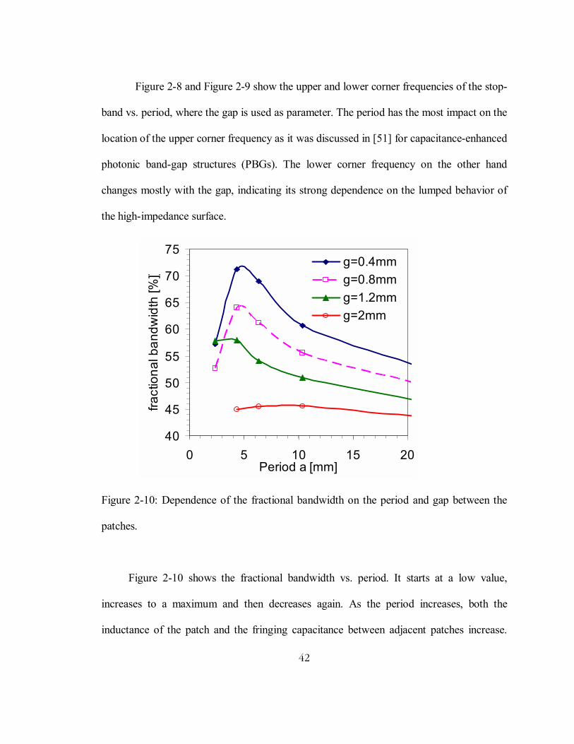
42
Figure 2-8 and Figure 2-9 show the upper and lower corner frequencies of the stop-
band vs. period, where the gap is used as parameter. The period has the most impact on the
location of the upper corner frequency as it was discussed in [51] for capacitance-enhanced
photonic band-gap structures (PBGs). The lower corner frequency on the other hand
changes mostly with the gap, indicating its strong dependence on the lumped behavior of
the high-impedance surface.
40
45
50
55
60
65
70
75
0 5 10 15 20Period a [mm]
fract
iona
l ban
dwid
th [%
]]
g=0.4mmg=0.8mmg=1.2mmg=2mm
Figure 2-10: Dependence of the fractional bandwidth on the period and gap between the
patches.
Figure 2-10 shows the fractional bandwidth vs. period. It starts at a low value,
increases to a maximum and then decreases again. As the period increases, both the
inductance of the patch and the fringing capacitance between adjacent patches increase.

43
When the width of the patch is much larger than the via height, the total inductance of the
patch saturates against the sheet inductance of the regular parallel-plate wave guide given
by (1.34). This results in a saturation of the total sheet inductance, which is equal to sum of
the patch and via inductances. At this point the fractional bandwidth is at its maximum.
Any increase of the period beyond this value only increases the sheet capacitance, which
then leads to a decrease of the fractional bandwidth.
2.4 Power planes with nested high-impedance surfaces
2.4.1 Geometry description
So far we have discussed only cases, where either the ground or the Vdd plane was
replaced with a high-impedance surface. In this section we introduce the concept of nested
power planes, where the two plates are replaced with high-impedance surfaces. Figure 2-11
and Figure 2-12 show possible geometries for these structures that can be implemented on
a two-substrate three-metal layer PCB. The two outer layers are solid metal plates and the
intermediate or middle layer is used for the patches. In the power plane 1, the rows of
patches, either in the x- or z-directions, are alternatively connected to the ground or the Vdd
plane using straight vias. For the power plane of type 2, no two adjacent patches in the x- or
z-directions are connected to the same potential. In other words, patches on the same
diagonal are all connected to either the Vdd or the ground plane.

44
(a) (b)
Figure 2-11: (a) Top view and (b) cross section of two calls of nested plane 1. Dashed lines
represent the Vdd plane and solid lines represent the Gnd plane.
In order to validate the concept, we consider three different power plane pairs of
lateral dimensions 10 cm x 10 cm each. The patches have square shapes of period 10 mm
with a gap of 1 mm between adjacent patches. The height of each HIS is 1.54 mm. For the
simplicity the vias have square cross section of 0.4 mm x 0.4 mm and the substrate is
lossless FR4 with a dielectric constant of 4.4.
(a) (b)
Figure 2-12: (a) Top view and (b) cross section of a unit cell of nested plane 2. . Dashed
lines represent the Vdd plane and solid lines represent the Gnd plane.
2cm
2cm
1cm
1cm
10mm

45
0
1
2
3
4
5
6
7
8
0 10 20 30 40 50
Freq
uenc
y [G
Hz]
Mode 1Mode 2Mode 3
X−ΜΓ−X Μ−Γ
BAND-GAP
Figure 2-13: Dispersion diagram of nested plane 1.
2.4.2 Simulation and discussion of results
The dispersion diagram of the nested plane 1 was extracted over the entire Γ-X-M
triangle and is shown in Figure 2-13 for the first three modes. On the Γ-X and X-M
portions of the triangle, the first mode is a slow-wave TMn mode that is tightly bound to
the surface. The group velocity (dω/dβ) of this mode is positive on the Γ-X and X-M
sections of the triangle, where the phase constant is positive, and negative on the on the M-
Γ segment, where the phase constant is negative. This implies that this mode is forward

46
propagating as a slow wave. The second mode is a TMn surface wave, which falls exactly
on the first mode on the X-M portion of the triangle. In the Γ-X and M-Γ portions, it has a
negative group and a positive phase velocities respectively and therefore corresponds to a
backward propagating wave. The third mode is an undisturbed TEn mode, which has its
cutoff frequency at about 3.6 GHz. The forbidden band-gap of this nested plane resides
between the second and third modes and is between 2.4 GHz and 3.6 GHz.
0
1
2
3
4
5
6
0 50 100 150
phase [degrees]
Freq
uenc
y [G
Hz]
Mode 1
Mode 2
Mode 3
Figure 2-14: Dispersion diagram of nested plane 2. Only Γ-X portion is presented.
The dispersion diagram of the nested plane 2 is shown in Figure 2-14 for the first
three modes. The first mode is a forward traveling surface-bound TMn wave. The second

47
mode is a backward mode that coincides with the first mode in the X-M portion of the
triangle. The third mode is a forward propagating TEn mode. For this power plane pair, the
band-gap corner frequencies are not clearly defined.
Figure 2-15 shows the insertion loss of the two nested power planes along with that
of a non-nested power plane (reference plane) of similar geometry. The emitting and
receiving ports are placed at (5 cm, 2 cm) and (5 cm, 5 cm) respectively. The nested plane
1 has an effective shift of the upper corner frequency with respect to the reference structure.
The lower corner frequency is about the same. The nested plane 2 exhibits a shift of the
upper and lower corner frequencies towards lower frequencies with a simultaneous
shrinking of the band-gap. The latter also shows some resonance mitigation at much lower
frequencies, which corresponds to increased embedded capacitance between the ground
and Vdd planes. This is even more important as decreasing the space between the patches
will further increase the embedded capacitance and therefore eliminate the need for
dissipative edge terminations. The insertion loss of the three power planes with the gap
reduced from 1 mm to 0.2 mm is shown in Figure 2-16.

48
Figure 2-15: Insertion loss of nested vs. non nested power planes, g = 1 mm.
Figure 2-16: Insertion loss of nested vs. non nested power planes, g= 0.2 mm.

49
2.5 Experimental verification
The concept of power planes with integrated standard HIS has been verified
experimentally. Several structures with patch size varying from 2 mm to 20 mm and
constant gap of 400 µm have been fabricated and characterized using a two-port network
analyzer. In the experimental setup the Vdd plane is a solid metallic plate and the Gnd
plane only has 4 rows of HIS cells separating the emitting and the receiving ports as
illustrated by the example of Figure 2-17. The thickness of the structure was 3.08 mm,
which consists of 1.54 mm for the HIS and 1.54 mm for the distance between the HIS and
Vdd plane. The fabrication was realized in a commercially available typical PCB
technology. In Table 2-2 we summarize the measured power plane characteristics, which
were also in good agreement with performance obtained from the simulated dispersion
diagram.
Design Number
Patch Width (mm)
Lower corner
Frequency (GHz)
Upper corner
Frequency (GHz)
Bandwidth (GHz)
Relative Bandwidth
1 5 4.2 8.4 4.2 66% 2 6 3.6 7.1 3.5 65% 3 8 2.7 5.2 2.5 63% 4 10 2.2 4 1.8 58% 5 15 1.6 2.9 1.3 57% 6 20 1 1.75 0.75 54%
Table 2-2: Extracted characteristics of fabricated power planes with integrated high-
impedance surface. g= 0.4 mm, t=d=1.54 mm, εr= 4.1.
Measured S-parameters for a typical power plane are shown in Figure 2-18. There
is a wide frequency bandgap between 2.2 and 4.0 GHz as expected for that geometry. The

50
signal transmission level is also very low at very high frequencies. This transmission drop,
which is actually good for the resonance attenuation, can be primarily inferred to the
resistive and dielectric losses.
Figure 2-17: Experimental setup for power planes with integrated HIS. Measurement is performed using SMA connectors on both sides of the four HIS rows.
SMA2
2x1.54mm
SMA2

51
0 2 4 6 8 10 12 14 16 18 20-80
-70
-60
-50
-40
-30
-20
-10
0
Frequency (GHz)
S12 in dB
Figure 2-18: Measured insertion loss of a 10 cm x 10 cm power plane with cells of period
10 mm and gap of 0.8 mm.
2.6 Summary
A novel concept for mitigating simultaneous switching noise in power planes of
high-speed circuits has been developed. The concept consists of replacing at least one plate
of the power plane pair with a high-impedance electromagnetic surface. Simultaneous
switching noise, which is reduced by mitigating the ground bounce observed in traditional
power planes is strongly dependent on the frequency region, where the HIS has its
forbidden band-gap. Contrary to the approaches reported previously in the literature, HIS
can mitigate SSN in all directions and, therefore, represents a global solution. Using a
systematic analysis, the impact of the geometrical parameters of the HIS on its ability to
mitigate noise has been studied. Usually large lattice constants (or periods) and small gaps
between the patches are required to achieve SSN immunity at very low frequencies. The
concept of nested power planes, which consists of replacing both plates of the power plane

52
pair with high-impedance electromagnetic surfaces without increasing the PCB thickness
(in comparison with planes with standard HIS on either Gnd or Vdd plane), has also been
introduced. The latter provides a smaller bandwidth for noise mitigation and the bandgap is
located between the second and third modes. In addition, the close proximity of the planes
can lead to noise suppression at very low frequencies without use of DC decoupling
capacitors.
53
Chapter 3
3 Inductively-Tuned High-Impedance Electromagnetic
Surfaces Integrated in Power Plane Environments
3.1 Introduction
High-impedance electromagnetic surfaces (HIS), as discussed in [15], have two
fundamental limitations for low frequency designs. For a given technology, where the
dielectric constant is fixed, a decrease in the center frequency can only be reached by
increasing either the inductance per unit area or the capacitance per unit area. A substantial
increase of the sheet inductance can only be reached by increasing the via height [54]. If
the thickness of the substrate has to be kept minimum the latter approach is not optimum
and the only remaining alternative is the enhancement of the per unit area capacitance,
which can be obtained by increasing the period of the structures or by minimizing the gap
or spacing between adjacent patches. In recent years, there has been substantial research
work [58]-[62] towards the design of high-impedance electromagnetic surfaces (HIS) or
electromagnetic band-gap structures (EBG) for low frequency designs, all of which was
focused on enhancing the per unit area capacitance of the high-impedance surfaces. In [58]
and [59] the capacitance enhancement was obtained by using double-layer patches. In this

54
case, the fringing capacitance between adjacent cells is comparable to that of the parallel
plate capacitors. For such structures a low-loss high-k dielectric constant can be used
between the patches, while a high-loss dielectric is used in the other regions. Obviously the
implementation of this approach in standard PCB technology requires an increase of the
number of metal layers. In [59], the patches on the second layer were modified to
concentric rings. This minimizes the area of the top patch that does not have a direct
overlap with the patch of the first layer and therefore contributes less to the fringing
capacitance. In [60] a two-layer HIS was designed with micro-electromechanical systems
(MEMS) switches between the patches. External DC voltages were then used to tune the
capacitance of the MEMS, which adds to the capacitance of the HIS to enhance the overall
capacitance performance. In [61] and [62], the MEMS switch was replaced by other
components with voltage variable capacitance such as varactors, MOS capacitors and PiN
diodes in a single layer HIS. This capacitance enhancement led to devices with operating
frequencies in the 1 to 2 GHz range, but the use of power to operate the HIS as well as the
noise associated with active devices remains a major drawback. While most attention has
been focused on designing for low frequencies, only little attention has been paid to the
importance of the actual bandwidth as most designs such as antennas are usually
narrowband. In designing HIS for application in power planes of high-speed circuits it is
very important to examine the ability of these structures to mitigate SSN over a broad
frequency range. In this case tradeoffs may be required between the per unit area
inductance and the per unit area capacitance to meet both the center frequency and the
bandwidth requirements.

55
This chapter introduces various novel concepts for designing high-impedance
electromagnetic surfaces with forbidden frequency band-gap at low frequencies. These
concepts are based on enhancing the inductance per unit area with little or no increase on
the overall thickness of the board. All structures are primarily evaluated in conjunction with
their application in mitigating simultaneous switching noise in parallel-plate power planes.
In section 3.2 we discuss the concept of power planes with double-layer inductance-
enhanced HIS and its combination with dissipative edge termination (DET) for broadband
noise mitigation. Three types of power planes with single layer inductively-tuned high-
impedance surfaces are discussed in section 3.3. Section 3.4 discusses the size optimization
of HIS with spiral inductor patches to improve noise mitigation and increase the IC
packaging density and the work is concluded in section 3.5.
3.2 Two-layer HIS with inductance-enhanced vias
3.2.1 Power plane with inductance-enhanced vias
The two-layer inductance-enhanced high-impedance surface is realized by
replacing the straight via of the single-layer HIS with an inductive element such as the one
illustrated in Figure 3.1. Its implementation in a power plane is shown in Figure 3.2. The
inductive element consists of a single loop conductor, which is connected to the patch and
the bottom metallic plate using an upper and a lower via respectively. The overall per unit
cell or per unit area inductance enhancement due to the use of this element can roughly be
approximated by the sum of the self-inductance in nanohenry (nH) of the individual
segments (3.1) also known as Greenhouse formula [63]

56
+
++
+
=∑= i
ii
ii
in
ii l
twtw
llL
350049.0
2ln2
1
(3.1),
where li, wi, and ti represent the length in cm, the width in cm and the thickness in cm of
each segment. N is the total number of segments. Depending on the size of the patches and
the inductance per unit area requirement, the intermediate conductor, which is in effect an
inductor, can be designed to have more (or even less) than one turn and can also be
distributed on several layers without impacting the periodicity of the high-impedance
surface. This is especially important if SSN mitigation below 1 GHz is desired. Since the
area required by the inductor is very small, unwanted inductive coupling with adjacent cells
is also minimized. In a power plane environment the HIS with multi-turn spiral inductor is
expected to behave similarly to power planes using HIS with long single-loop inductor as
both approaches mainly contribute to an increase in inductance.
upper via
lower via
half-loop inductornormal to the vias
Figure 3-1: Single-loop inductive element for inductance enhancement.
This novel concept of extending the conductor in the direction perpendicular to the via
achieves the following two important objectives:

57
• It allows increased inductance without increasing the overall PCB thickness.
• It introduces a degree of freedom that allows fine-tuning of the inductance while
keeping the capacitance constant.
By using a multi-turn or spiral inductor, the inductance per unit area is increased
significantly. In fact the total inductance per unit cell increases to
MLLt += (3.2),
where L is the self inductance of the individual segments given by equation (3.1) and M is
the total mutual inductance between the individual segments of the inductor. The mutual
inductance between two parallel coplanar metal segments (of the spiral inductor) is given
by equation (3.3) and is equal to zero when the segments are orthogonal. In addition mij is
negative when the current in the segments flows in opposite directions, such that for a
square spiral inductor segments on the same site have positive mutual inductance between
them and segments on opposite side have negative mutual inductance between them.
++−
++=
ij
ij
ij
ij
ij
ij
ijijij l
dld
dl
dlm 2
2
2
2
111ln2 (3.3)
In equation (3.3) lij is the length of the segments and dij is the center-to-center distance
between the parallel segments i and j. From equation (3.3) the total mutual inductance can
be calculated as (3.4)
∑∑= =
=n
iij
n
jmM
1 121 (3.4).

58
top plate
bottom platea
lower viaupper via
Surface patches
(a)
g
a
(b)
Figure 3-2: (a) Cross section and (b) top view of power plane with double-layer
inductance-enhanced HIS.
The performance of the power plane with two-layer inductance-enhanced HIS was
evaluated by considering a 10 cm x 10 cm power plane. The total thickness of the power
plane including HIS was fixed at 1.54 mm. This corresponds to upper and lower via heights
of 0.5 mm and a substrate of thickness 0.5 mm between the top of the HIS and the top
plate. Square patches were used with the separation between adjacent patches fixed at 0.4

59
mm. The substrate was lossless FR4 of dielectric constant 4.4. Copper was used as
conductor material. The period was 10 mm and the ports located at (4.5 cm, 1.5 cm) and
(4.5 cm, 4.5 cm). Here the ports were between the Vdd plane and the top of the HIS.
Different simulations were then performed with the length of the single-loop conductor
varying from 5 mm to 16 mm. Figure 3.3 shows the insertion loss for the two extreme
cases. If we consider the -30 dB bandwidth as the stop-band of the power plane, we notice
that the fractional bandwidth increases with the loop length. At the same time theres a
decrease in the bandwidth, suggesting that for any given structure the noise mitigation
capability would also saturate as the inductance increases. More importantly, resonance
suppression is achieved down to 700 MHz without any major increase of the power plane
thickness. It is also important to point out that the location and width of the stop-band
would vary if the ports are between the Vdd plane and the bottom of the HIS.
Figure 3-3: Effect of inductor loop length on insertion loss.

60
3.2.2 Combination of HIS with dissipative edge termination (DET)
In power planes with finite dimensions, the low-inductance bypass capacitance of
the planes is of vital importance in mitigating simultaneous switching noise. But this by-
pass capacitance does not mitigate resonances induced by standing waves and edge
radiation, which are very pronounced at very low frequencies. Inherent dielectric and
conductor losses can help mitigate these resonances up to a certain extent [64]-[66]. These
resonances can also be reduced by using either capacitive or resistive terminations along
the edge of the PCB. In [67], a design methodology was proposed for the determination of
dissipative edge termination for traditional power planes. The dissipative edge elements
consist of series ReCe, where Ce acts as a decoupling capacitor between the Vdd and the
ground planes since they have to be at different potential, and Re is selected according to
equation (3.5)
ue ZR 02= (3.5),
where Z0u is the characteristic impedance of a square unit cell given by
ruu W
hZε
π1200 = (3.6).
In (3.6), h is the height of the power plane pair and Wu is the width of the unit cell. To
assure effective termination up to a given frequency f0, the spacing Wu between the
termination components, which is also the width of the unit cell, has to be smaller than
10% of the wavelength at the highest frequency f0 of interest and Re has to be less than the
impedance ω0Le of the parasitic edge inductance associated with the discrete. As it was

61
discussed in the previous chapter the parasitic inductance associated with the components is
fixed, but the value of Re varies with Wu according to (3.5)-(3.6).
As it is shown in Figure 3.4 the inductance-enhanced HIS can mitigate SSN down
to the low GHz frequencies, but there is still a very strong resonance close to DC
frequencies. In order to evaluate the impact of dissipative edge termination on power planes
with integrated HIS, we consider a 10 cm x 10 cm power plane of type shown in Figure
3.2. The upper and lower vias are of length 1 mm each. The period of the lattice is 10 mm
and the gap between the hexagonal patches, g, is 0.4 mm. The top plate is placed 1 mm
above the patches. The transmission characteristics S12 are plotted together with those of a
simple parallel-plate structure of same height with and without a wall of RC pairs placed
around the edges of the board (the inductance of the capacitor leads, Le is included as
before) in Figure 3.4. A total of 40 ReCe pairs were uniformly placed around the PCB, with
Re=5.36 Ohms and Ce=1 nF and Le=0.5 nH. The resistance of the RC combination is
selected to match the impedance of the simple parallel- plate system as in [68]. The wall of
capacitors offers a good SSN mitigation capability at lower frequencies. For higher
frequencies, however, the noise suppression capability of the HIS is remarkable. In fact, the
frequency width of the resulting -20 dB band-gap is approximately 3.3 GHz. Over the
band-gap, the HIS significantly diminished the surface waves that travel within the plates,
which in turn results in significantly reduced Q for the parallel-plate cavity.

62
-80
-70
-60
-50
-40
-30
-20
-10
0
0 0.5 1 1.5 2 2.5 3 3.5 4
power plane with HIS and wall of RCtraditional power planepower plane with wall of RC
Figure 3-4: Transmission characteristics of a 10 cm x 10 cm power plane with RC
dissipative edge termination and combination of RC dissipative edge termination and HIS.
3.3 Power planes with single-layer inductive-enhanced high-impedance surfaces
The fundamental idea behind the single-layer inductance enhanced HIS consists of
bringing the inductance-enhancing loop (or its equivalent) to the same layer as the patch
and in series with the via. This would result in an effective increase of the via inductance.
For very low frequency design and bandwidth considerations a substantial increase in
inductance per unit area should not always lead to a strong decrease of the per unit area
capacitance. The structures considered in this section all have a period of 10 mm with a gap
or spacing of 1 mm between adjacent patches. The substrate is lossless FR4 of dielectric

63
constant 4.4 and the thickness of a single layer is 1.54 mm. For the power plane or parallel-
plate waveguide configuration, this is equivalent to a total thickness of 2 layers, where one
layer is used for the HIS and the other layer is the substrate between the Vdd and the
ground planes. The conductor material is perfect conductor. The initial analysis of the
structures is done by calculating the dispersion diagram based on the unit cell as it was
described in section 1.8.1.
3.3.1 Power planes using single-layer cross structure
3.3.1.1 Structure topology
The top-view of the cross structure unit cell is shown in Figure 3.5. It is realized
by altering the patch of the standard Sievenpiper structure at its center to include a metallic
cross. The cross fingers can be considered as narrow transmission line segments, whose
inductance effectively adds to that of the via to increase the total sheet inductance or
inductance per unit area. For fixed via height, period and gap, the impedance of the surface
can be controlled by varying nf, wf, lf or gf, which represent the number, width, length of
fingers as well as the gap between the finger and the rest of the patch as illustrated in
Figure 3.5. Small finger width and large gf both increase the sheet inductance. It can also be
expected that the qualitative effect of the period and patch separation will be similar to that
of the standard HIS.

64
gf
a
lf
Wf
W
g/2
Figure 3-5: Top view of the cross structure unit cell with design parameters indicated. The
circle at the center is the via connecting to the bottom plate.
3.3.1.2 Structure simulation and discussion of results
The effect the number of fingers on the power plane performance was evaluated
using electromagnetic (EM) simulation, where the Γ-X portion of the dispersion diagram
was calculated for three structures having nf=4, 2 and 1 as variable, while the other
parameters were fixed at lf=2.5 mm, gf=0.25 mm, Wf=0.5 mm, W=9 mm and g= 1 mm.
Figure 3.6 shows the dispersion diagram of the structures, where only the first two modes
that determine the location of the band-gap (or stop-band) are plotted. The resulting stop-
band locations are summarized in Table 3.1. When the number of fingers is equal to 4, the

65
4 transmission line segments are electrically almost in parallel, leading therefore to an
inductance contribution that is comparable to one fourth of the inductance of a single
finger. The inductance is maximal, when the number of fingers is equal to one. In this case
the center frequency has the lowest value, as expected.
Figure 3-6: Effect of number of fingers on the stop-band location and width.
Filled symbols correspond to upper band edge, whereas non-filled symbols correspond to
lower band edge, lf=2.5 mm, gf=0.25 mm, Wf=0.5 mm, W=9 mm, g= 1 mm.

66
Structure ID
Number of fingers
Lower corner frequency [GHz]
Upper Corner Frequency [GHz]
Bandwidth [GHz]
Cross 1 4 2.14 3.7 1.56 Cross 2 2 1.97 3.4 1.43 Cross 3 1 1.67 2.8 1.13
Table 3-1: Summary of the location and width of the band-gap of power planes with single-
layer cross high-impedance surface, lf=2.5 mm, gf=0.25 mm, Wf=0.5 mm, W=9 mm, g= 1
mm.
Figure 3-7: Top view of unit cell of single-layer of HIS unit cell with closed loop spiral.
3.3.2 Power planes using single-layer HIS with closed loop spiral as patch
3.3.2.1 Structure topology
Figure 3.7 shows the top view of the general topology of the patch used in the
high-impedance electromagnetic surface with closed loop spiral. It is obtained by opening a
hole at the center of the patch of the standard Sievenpipers cell, where a spiral inductor is
inserted. The spiral inductor has one end connected to the via and the other end connected
to the rest of the patch. An estimate of the inductance enhancement due to the spiral can be

67
obtained from equation (3.4). The surface impedance can be controlled by varying the
geometrical parameters of the inner inductor, which the inner diameter, the number of
turns, the line width and the line spacing. In order to achieve a large inductance value with
simultaneously large fringing capacitance, the outer turn or loop has to maintain a large
width, whereas the inner spiral inductor should have narrow metal traces, with narrow
spacing between the turns as well as a large number of turns. As the number of turns of the
spiral inductor increases the surface inductance increases very fast, leading to the lowering
of the center frequency. At the same time there is a decrease in the absolute bandwidth. In
order to achieve wideband design at low frequencies, the high number of turns can be
combined with a smaller period as will be shown in section 3.4.
g/2
l1
l2
a
W
Ws
W1W3
W2
W4
g/2
l1
l2
a
W
Ws
W1W3
W2
W4
Figure 3-8: Implementation of the single-layer HIS with closed loop for a lattice constant of
10 mm.

68
3.3.2.2 Simulation and discussion of results
The initial validation of the concept was done by simulating the structures based on
the unit cell of Figure 3.8, where the spiral inductor is limited to two transmission line
segments. The detailed geometrical parameters were W=9 mm, g=1 mm, a=10 mm,
W1=3.5, W2=W3=W4=2.5 mm, l1=1.5 mm, l2= 2 mm, Ws = 0.5 mm. A much significant
increase of the inductance would result in a stop-band that is in the hundreds MHz range.
The Γ-X section of the dispersion diagram was calculated and is shown in Figure 3.9.
Figure 3.10 shows the insertion loss of a parallel-plate power plane based on a 10 x 10
array of the unit cell of Figure 3.9. Here the distance between the transmitting and
receiving ports was 30 mm or three unit cells. Both graphs show that power planes with
this HIS would provide parallel-plate mode immunity in the frequency range from 1.7 GHz
to 2.7 GHz, which is a much lower frequency range than that of power planes with standard
HIS of same period, gap and material properties.

69
Figure 3-9: Dispersion diagram of power plane using single-layer HIS with outer loop
closed spiral. W=9 mm, g=1 mm, a=10 mm, W1=3.5, W2=W3=W4=2.5 mm, l1=1.5 mm,
l2= 2 mm, Ws = 0.5 mm.
Figure 3-10: Insertion loss of structure with closed open loop, W=9 mm, g=1 mm, a=10
mm, W1=3.5, W2=W3=W4=2.5 mm, l1=1.5 mm, l2= 2 mm, Ws = 0.5 mm.

70
3.3.3 Power planes using HIS with open loop spiral inductors as patch
3.3.3.1 Structure topology
Figure 3.11 shows the top view of the patch used in the HIS with open loop spiral
inductor. It is obtained by opening the outer loop of the structure of Figure 3.7. The surface
impedance is controlled by varying the geometrical parameters of the spiral inductor, which
include the inner diameter, the line width, the line spacing and the number of turns.
Figure 3-11: Top view of HIS unit cell with open loop spiral inductor as patch.

71
g/2
l1
l2
a
W
Ws
W1W3
W2
W4
s
g/2
l1
l2
a
W
Ws
W1W3
W2
W4
s
Figure 3-12: Implementation of the HIS with open-loop spiral inductor. Inner inductor has
quarter turn.
3.3.3.2 Simulation and discussion of results
To evaluate the performance of these types of structures, the structure of Figure 3-
12 was simulated using HFSS, whereby the following geometrical parameters were used:
s=0.4 mm, W=9 mm, g=1 mm, a=10 mm, W1=3.5, W2=W3=W4=2.5 mm, l1=1.5 mm, l2=
2 mm, Ws = 0.5 mm. Both the insertion loss based on a 10 x 10 array and the dispersion
diagram based on the eigenmodes of the unit cell have been calculated. Figure 3-13 shows
the full Γ-X-M-Γ dispersion diagram of the structure. Two forbidden band-gaps are
exhibited, one from 1.15 to 1.75 GHz and the other from 3.42 GHz to 3.75 GHz. Figure 3-
14 shows the insertion loss vs. frequency for the same structure. The -20 dB band-gaps are
exactly the same as those predicted by the dispersion diagram. In addition there is a global
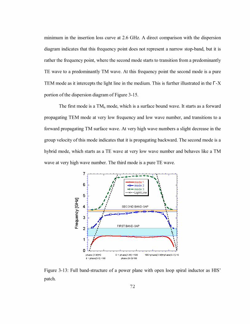
72
minimum in the insertion loss curve at 2.6 GHz. A direct comparison with the dispersion
diagram indicates that this frequency point does not represent a narrow stop-band, but it is
rather the frequency point, where the second mode starts to transition from a predominantly
TE wave to a predominantly TM wave. At this frequency point the second mode is a pure
TEM mode as it intercepts the light line in the medium. This is further illustrated in the Γ-X
portion of the dispersion diagram of Figure 3-15.
The first mode is a TMn mode, which is a surface bound wave. It starts as a forward
propagating TEM mode at very low frequency and low wave number, and transitions to a
forward propagating TM surface wave. At very high wave numbers a slight decrease in the
group velocity of this mode indicates that it is propagating backward. The second mode is a
hybrid mode, which starts as a TE wave at very low wave number and behaves like a TM
wave at very high wave number. The third mode is a pure TE wave.
Figure 3-13: Full band-structure of a power plane with open loop spiral inductor as HIS
patch.

73
Figure 3-14: Insertion loss of the structure with open outer loop. A 10 cm x 10 cm power
plane was considered with a separation of 3 cm between the emitting and receiving ports.
Figure 3-15: Dispersion diagram of the structure with open outer loop.

74
More insights on the nature of the propagating waves can be gained by looking at
the electrical and magnetic field plots between the top of the HIS and the Vdd plane for
different wave numbers. Based on the Γ-X section of the dispersion diagram three different
wave numbers have been selected to capture the three regions of the second mode. Table
3.2 summarizes the eigenmode solutions for these three wave numbers. The dominant field
modes are obtained after comparison of the field intensity in x-, y- and z-directions are
shown in Figure 3-16a-h.
Phase angle[degrees] Mode 1 [GHz] Mode 2 [GHz] Mode 3 [GHz] 40 0.99 2.17 3.7 70 1.28 2.72 3.9 110 1.365 3.124 4.82
Table 3-2: Eigenmode solutions of the parallel-plate power plane using HIS with open
outer loop open spiral inductor.

75
(a) Electric and magnetic fields of mode 1 at 40 degrees.

76
(b) Electric and magnetic fields of mode 2 at 40 degrees.

77
(c) Electric and magnetic fields of mode 3 at 40 degrees.

78
(d) Electric and magnetic fields of mode 2 at 70 degrees.

79
(e) Electric and magnetic fields of mode 1 at 110 degrees

80
(f) Electric and magnetic fields of mode 2 at 110 degrees

81
(h) Electric and magnetic fields of mode 3 at 110 degrees
Figure 3-16 (a)-(h): Electromagnetic field plots at different phase angles
3.3.3.3 Effect of varying the location of the outer-loop slot
The variation of the width, s, of the slot from 0.1 to 1 mm does not show a
significant difference on the performance of the power plane. The relative location of the
slot on the outer loop was changed to the opposite site. Table 3.3 summarizes the relative
position of the band-gap. For comparison the attributes of the same structure without slot
are also included.

82
Description of outer loop a [mm] W1-4 [mm] Band-gap 1 [GHz]
Band-gap 2 [GHz]
closed 10 2.5 1.52-2.46 None open 10 2.5 1.15-173 3.24-3.5
open on opposite side 10 2.5 1.49-2.35 2.74-2.83
Table 3-3: Relative position of the outer loop slot on the location and size and band-gaps,
Ws= 0.5 mm, l1=1.5 mm, l2=2.25 mm, g=1 mm.
0
0.5
1
1.5
2
2.5
3
3.5
4
0 0.2 0.4 0.6 0.8 1k/pi[1/cm]
Freq
uenc
y[G
Hz] Mode 1
Mode 2Mode 3Mode 1Mode 2Mode 3
Figure 3-17: Effect of varying the gap size on the dispersion diagram of the power plane
using an open loop spiral inductor as patch.
3.3.3.4 Effect of the gap width
Figure 3.17 shows the dispersion diagram of the cell, where the patch separation g
between adjacent patches has been varied from 1 mm to 0.4 mm. This is done by increasing
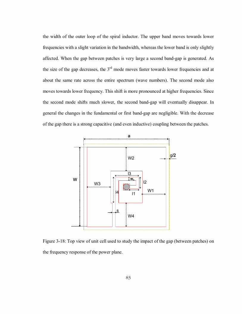
83
the width of the outer loop of the spiral inductor. The upper band moves towards lower
frequencies with a slight variation in the bandwidth, whereas the lower band is only slightly
affected. When the gap between patches is very large a second band-gap is generated. As
the size of the gap decreases, the 3rd mode moves faster towards lower frequencies and at
about the same rate across the entire spectrum (wave numbers). The second mode also
moves towards lower frequency. This shift is more pronounced at higher frequencies. Since
the second mode shifts much slower, the second band-gap will eventually disappear. In
general the changes in the fundamental or first band-gap are negligible. With the decrease
of the gap there is a strong capacitive (and even inductive) coupling between the patches.
a
g/2
W4
W2
W1W3 l2
l1
W
l4
l3
s
WS
a
g/2
W4
W2
W1W3 l2
l1
W
l4
l3
s
WS
Figure 3-18: Top view of unit cell used to study the impact of the gap (between patches) on
the frequency response of the power plane.

84
A further study of the effect of the gap was performed by studying the structure of
Figure 3.18, where the portion of the inductor with the smaller line width has been
extended to a full turn. The width and location of the stop-bands are summarized in Table
3.4. It can be seen that when the gap goes beyond a certain value the second band-gap
vanishes.
Structure A [mm]
G [mm]
W1-4 [mm]
Ws [mm]
Band-gap 1 [GHz]
Band-gap 2 [GHz]
1 5.4 1.2 1.1 0.2 2.12-3.1 6.55-8.89 2 5.4 0.6 1.4 0.2 1.94-3.1 6.2-6.2 3 5.4 9.4 1.5 0.2 1.89-3.1 None 4 10 5.2 1.4 0.2 1.9-2.26 5.8-6.14 5 10 0.6 3.9 0.2 1.1-1.8 None
Table 3-4: Effect of the gap size on the location and width of the band-gaps, l1=0.6 mm,
l2= 0.7 mm, l3=1.5 mm, l4= 1.6 mm, s=0.2 mm.
3.4 Design of power planes using high-impedance electromagnetic surfaces with a
period of 5 mm
In the previous sections the concept of power planes with single-layer inductively-
tuned HIS was demonstrated using cells with a period of 10 mm. As it was reported in [69],
for power planes with integrated HIS, efficient noise mitigation is achieved at distances of
at least two periods away from the noise source. This implies that the smaller the period,
the smaller the distance required between individual ICs on a PCB for high level noise
immunity. At the same time this will lead to a high packaging density. In this section we
investigate the possibility of using smaller periods to achieve SSN mitigation in the same

85
order as previously described for larger periods. For all structures the via height and the
substrate height between the HIS and the Vdd plane are fixed to 1.54 mm. The period of
the HIS is 5 mm. The via diameter is 0.4 mm. The structures are first evaluated with a gap
g (separation between adjacent patches) of 0.6 mm. The main electrical performance
attributes of interest are the bandgaps or stopbands, which are all derived from the Γ-X
section of the dispersion diagram.
0
2
4
6
8
10
12
14
16
0 50 100 150 200Phase ka [degrees]
Freq
uenc
y [G
Hz]
mode 1mode 2mode 3
Figure 3-19: Dispersion diagram of reference power plane with standard HIS, a=5 mm, g=
0.6 mm, w= 4.4 mm, t=d= 1.54 mm.
A reference power plane cell with the standard HIS is first analyzed and the
resulting dispersion diagram shown in Figure 3-19. It has a single band-gap between 4 GHz

86
and 8 GHz. This band-gap resides between the first and second modes, which are TMn and
TEn respectively. It can also be seen that when the phase constant is about 110°, the 2nd and
3rd mode swap.
Figure 3-20: Top view of HIS unit cell with single-turn fat spiral as patch
Figure 3-20 shows the top view of the modified reference patch, where a 0.2 mm wide slot
has been opened in the patch to change it into a single-turn fat inductor. The
corresponding dispersion diagram is shown in Figure 3-21a. The fundamental band-gap is
from 3.15 to 5.02 GHz and resides between the first and second modes. In this case a
second band-gap, as expected for large values of g, is exhibited, between 7.72 and 8.2 GHz.
In the dispersion diagram of Figure 3-21b, the gap size has been reduced to 0.1 mm. In
general the changes in the fundamental or first band-gap are negligible. With the decrease
of the gap there is a strong capacitive (and inductive) coupling between the patches. The
negative slope seen in the first mode has been described in [70] for the open HIS as an
indication of a backward traveling surface wave.

87
0
2
4
6
8
10
12
0 50 100 150 200Phase ka [degrees]
Freq
uenc
y [G
Hz]
mode 1mode 2mode 3
g=0.6mm
(a)
(b)
Figure 3-21 : Dispersion diagram of power plane unit cell with single turn fat spiral as
patch for patch separation of (a) 0.6 mm and (b) 0.1 mm. Slot on outer loop is 0.2 mm
wide.
0123456789
10
0 50 100 150 200Phase ka [degrees]
Freq
uenc
y [G
Hz]
mode 1mode 2mode 3 g=0.1mm
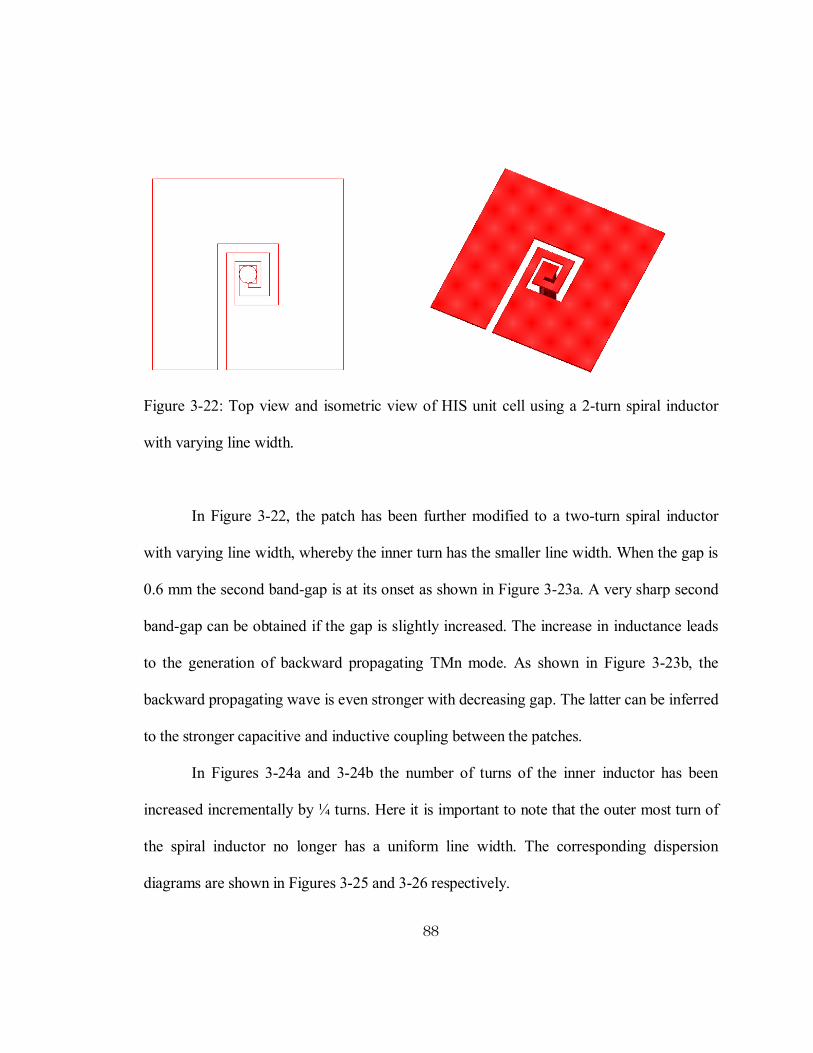
88
Figure 3-22: Top view and isometric view of HIS unit cell using a 2-turn spiral inductor
with varying line width.
In Figure 3-22, the patch has been further modified to a two-turn spiral inductor
with varying line width, whereby the inner turn has the smaller line width. When the gap is
0.6 mm the second band-gap is at its onset as shown in Figure 3-23a. A very sharp second
band-gap can be obtained if the gap is slightly increased. The increase in inductance leads
to the generation of backward propagating TMn mode. As shown in Figure 3-23b, the
backward propagating wave is even stronger with decreasing gap. The latter can be inferred
to the stronger capacitive and inductive coupling between the patches.
In Figures 3-24a and 3-24b the number of turns of the inner inductor has been
increased incrementally by ¼ turns. Here it is important to note that the outer most turn of
the spiral inductor no longer has a uniform line width. The corresponding dispersion
diagrams are shown in Figures 3-25 and 3-26 respectively.

89
(a)
(b)
Figure 3-23: Dispersion diagram of a 2-turn spiral inductor with varying line width and a
gap of (a) 0.6 mm and (b) 0.1 mm.
0123456789
10
0 50 100 150 200Phase ka [degrees]
Freq
uenc
y [G
Hz]
mode 1mode 2mode 3 b) g=0.1mm
0
2
4
6
8
10
12
0 50 100 150 200Phase ka [degrees]
Freq
uenc
y [G
Hz]
mode 1mode 2mode 3 a) g=0.6mm

90
(a) (b)
Figure 3-24: Isometric view of HIS cell using (a) a 2-1/4 turn inner inductor and (b) a 2-1/2
turn spiral inductor with varying line width.
0
2
4
6
8
1 0
1 2
0 5 0 1 0 0 1 5 0 2 0 0P hase ka [d e g re e s ]
Freq
uenc
y [G
Hz]
m o d e 1m o d e 2m o d e 3
Figure 3-25: Dispersion diagram of structure with 2-1/4 turn spiral inductor as patch.

91
0
2
4
6
8
10
12
0 50 100 150 200Phase ka [degrees]
Freq
uenc
y [G
Hz
mode 1mode 2mode 3
Figure 3-26: Dispersion diagram of structure with a 2-1/2 turn spiral inductor as patch.
Several inductively-tuned HIS structures have been analyzed in a power plane
configuration, where a constraint was given on the maximum area for the unit cell. By
increasing the number of turns of the spiral, a substantial shift of the stop-band towards
lower frequencies could be achieved. It is further expected that additional increase of the
number of turns would lead to even lower center frequencies. This would also be
accompanied with a reduction of the width of the fundamental band-gap, which can
partially be compensated by designing the HIS to exhibit a second band-gap. Table 3.5
shows a summary of performance of all power planes discussed in this section.

92
Cell description
g [mm]
Band-Gap [GHz]
Center Freq. [GHz]
Bandwidth [GHz]
Fractional bandwidth [%]
standard 0.6 4-8.1 6.05 4.1 67.8 Single turn 0.6 3.15 - 5.02 4.085 1.87 45.8 Single turn 0.1 2.45 - 4.36 3.405 1.91 56 Two turn 0.6 2.34 - 3.74 3.04 1.4 46 Two-turn 0.1 1.96 - 3.57 2.765 1.61 58.2
Two and 1/4 0.6 1.87 - 2.85 2.36 0.98 41.5 Two and 1/2 0.6 2.15 - 3.37 2.76 1.22 44.2
Table 3-5: Location and width of the fundamental stop-band of power planes using various
HIS with open loop spiral inductor with variable line width, a=5 mm.
3.5 Conclusion
Novel types of high-impedance electromagnetic surfaces have been proposed and
studied in conjunction with their applications into parallel-plate power planes. The surface
impedance of these structures is primarily controlled by their sheet inductance. Using the
example of the double-layer HIS, it was shown that a combination of HIS and proper
dissipative edge termination (DET) can lead to power planes with broadband SSN
immunity starting at DC frequencies. Single-layer structures introduced here also showed
that HIS can be designed at very low frequency without increasing the height of the board
or the lattice constant. When the inductance is significantly increased in the HIS with open
loop spiral inductors, the fractional bandwidth of the fundamental band-gap becomes very
small. But at the same time there is a second bandgap, which allows dual-band switching
noise mitigation. It has also been shown that the two stopbands of the HIS with open-loop

93
spiral inductor can be tuned independently. In addition, the fact that the location of the
bandgaps is merely dependent on the lumped loading of the periodic structure enables
low-frequency designs with very small lattice constants, therefore leading to higher
packaging integration, when these HIS are used for noise mitigation in the power
distribution network of high-speed circuits.

94
Chapter 4
4 Development and Application of Physics-Based Compact
Models for High-Impedance Electromagnetic Surfaces
Integrated in Power Plane Environments
4.1 Introduction
As the physical size of electronic components increases, their analysis using
electromagnetic (EM) simulation becomes very lengthy and memory intensive. In some
cases, one could take advantage of the symmetry or of the periodicity to reduce the size of
the problem to be solved. The solution of the full problem is then obtained through post
processing of the simulation data. It is for example possible to represent a full
characterization of infinite periodic structures using dispersion diagrams obtained from the
electromagnetic (EM) simulation of a single cell. Practical limitations of the dispersion
diagram include their inability to predict how abrupt the transition from stop- to pass-band
regions may be or what is the level of signal attenuation at different regions of the
transmission curves. This complementary information can generally be obtained from the
scattering or S-parameters, which in most cases are generated from large structures with
finite dimensions. Transmission characteristics of one-dimensional periodic structures
using S-parameters obtained indirectly from the analysis of a single cell have been reported
in [24] and [52], where the interaction between individual cells is neglected. This

95
assumption allows the calculation of the transmission matrix of a long chain of cells by
chain-matrix multiplication of the ABCD-matrix of the individual cell. A more accurate
approach described in [71], and which includes cell-to-cell interaction, utilizes full wave
simulation to determine the overall transmission matrix of a limited number of cells. A
recursive formula is then used to derive the transmission matrix (ABCD) of the longer
chain. The two-port S-parameter matrix for the entire chain can then be obtained by using
the transformation (ABCD) to S-parameter transformation described in [24].
At frequencies where the physical length of transmission line based devices and
interconnects is much smaller than the wavelength, passive components can be modeled
using lumped-elements. This same approach can be applied to periodic structures as long as
the period is much smaller (one fifth) than the wavelength. In general lumped-element
equivalent circuits for one-dimensional two-port structures can be obtained from the two-
port Z- or Y-matrices. This concept, which has been applied intensively in the modeling of
traditional power plane pairs [72]-[75], describes the behavior of the system only with
respect to the ports by determining the transfer impedance. A more rigorous modeling of
power plane resonance has been demonstrated in [76]-[77], where the planes are divided
into identical cells and each cell modeled individually using either a lumped-element or a
transmission line approach. In either case the values of the model parameters can be
calculated using quasi-static formulation of the electromagnetic fields.
In general, compact models are combinations of physical and behavioral aspects of a
structure and can be obtained using numerical optimization to match measured or EM-
simulation-based S-parameters to those of the equivalent circuit. A very important point in

96
developing such models is the identification of a proper model form that incorporates the
physical effects of the components. Numerical optimization can then be used to determine
the right parameter values by optimizing measurement or EM-simulation data against those
of the equivalent circuit. While the lumped-element approach has been used to model
coplanar electromagnetic bandgap structures (EBGs) [84] or to explain the general
behavior of HIS [15], the most detailed approach for modeling HIS has been reported by
[17] and uses a transmission line approach.
This chapter introduces physics-based lumped-element compact models for HIS in
parallel-plate environment. The model form is first developed for a unit cell and several of
them connected in a two-dimensional array to build the model of large structures. Section
4.2 presents the development of the model form. Section 4.3 discusses the validation of the
model for power planes with integrated standard and double-layer HIS. The developed
compact model is applied in section 4.4 to study the mitigation of simultaneous switching
noise (SSN) across the power planes, and to determine the dissipative edge termination
(DET) requirements for broadband SSN mitigation. The extension of the compact model to
include frequency dependent resistive losses using only frequency-independent
components is discussed in section 4.5. The latter makes the model of particular interest for
integration in linear time domain simulators such as SPICE.

97
d
a
g/2
tµ, ε
µ, ε
µ, ε
patch
Vdd plane
w=
x
z
y
d
a
g/2
tµ, ε
µ, ε
µ, ε
patch
Vdd plane
w=
d
a
g/2
tµ, ε
µ, ε
µ, εµ, ε
patch
Vdd plane
w=
x
z
y
Figure 4-1: Cross-sectional view and decomposition of power plane unit cell into a parallel-
plate transmission line and HIS cells.
4.2 Compact model development
4.2.1 Model form definition for power planes using standard HIS
For the development of the model a power plane using a standard HIS with square
patches is considered. Figure 4-1 shows the cross sectional view of the power plane unit
cell and its decomposition into two effective cells for the HIS and the section between the
HIS and the Vdd plane. The latter can be approximated by a parallel-plate transmission
line, whereby it is important to note that the reference for this transmission line is the patch
of the HIS. For one-dimensional wave propagation the parallel-plate transmission line cell
can be modeled with the equivalent circuit of Figure 4-2a, where Lt is the total inductance
of the Vdd plane and Ct is the total capacitance between the patch and the Vdd plane.

98
Similarly the HIS cell can be modeled for one-dimensional wave propagation using the
equivalent circuit of Figure 4-3a, where Lp is the total inductance of the patch, Lv is the via
inductance, Cp is the total capacitance between the patch and the bottom plate of the HIS
and Cf is the fringing capacitance to the adjacent unit cell. The total capacitance between
the Vdd plane and the bottom of the HIS as well as the mutual inductance between adjacent
cells, which are not shown directly, are redistributed in the other components of the model.
Lt/2 Lt/2
Ct/2Ct/2
Lt/2 Lt/2
Ct/2Ct/2
(a)
Lt/2 Lt/2
Ct/4Ct/4
Ct/4
Ct/4
Lt/2
Lt/2
4
321
Lt/2 Lt/2
Ct/4Ct/4
Ct/4
Ct/4
Lt/2
Lt/2Lt/2 Lt/2
Ct/4Ct/4
Ct/4
Ct/4
Lt/2
Lt/2
4
321
(b)
Figure 4-2: Equivalent circuit of HIS unit cell for (a) one-dimensional and (b) two-
dimensional wave propagation with nodes 1-4 indicated.

99
For two-dimensional wave propagation the same model forms of Figures 4-2a and 4-3a
are used for the other main direction of propagation since the cells are square and
symmetric. This results in a 4-port compact model for both the transmission line and the
HIS cells as illustrated in Figures 4-2b and 4-3b respectively. The stacking (cascading) of
the two individual unit cell models results in the model of the power plane unit cell shown
in Figure 4-4.
Cp/2Cp/2
Lp/2Lp/2
Lv
2Cf2Cf
Cp/2Cp/2
Lp/2Lp/2
Lv
2Cf2Cf
(a)
Lp/2 Lp/2
Cp/4Cp/4
Cp/4
Cp/4
Lp/2
Lp/2
4
3
21
Lv
2Cf
2Cf
2Cf
2CfLp/2 Lp/2
Cp/4Cp/4
Cp/4
Cp/4
Lp/2
Lp/2
4
3
21
Lv
2Cf
2Cf
2Cf
2Cf
(b)
Figure 4-3: Equivalent circuit of parallel-plate transmission line for (a) one-dimensional
and (b) two-dimensional wave propagation with nodes 1-4 indicated.

100
The compact model of a full power plane can then be obtained by connecting
several of these unit cell models into a two-dimensional array. Figure 4-5 is an illustration
of the 2D-model of a large power plane using the cascading of many cells. Each rectangle
(box) is a multiport (10-port in this case) equivalent circuit of the unit cell. This compact
model form is very generic and can be used for power planes with inductance or
capacitance-enhanced HIS as well since the most significant difference resides only on the
via inductance.
Ct/4Ct/4
Rt/2
Cp/42Cf2Cf
2Cf
Cp/4
Cp/4
Cp/4
Lp/2
Rp/2 Lp/2 Lp/2Rp/2
Lp/2 Rp/2
Rt/2
Rt/2Lt/2Lt/2
Rt2 Lt/2
Ct/4Ct/4
Rv
Lv
Lt/2
Rp/2 2Cf
Figure 4-4: Full compact model of the power plane unit cell

101
Figure 4-5: Illustration of power plane compact model based on cascading of several unit
cell models.
4.2.2 Expansion of the model form to power plane using HIS with polygonal shapes
In general, when the polygonal patch has n sides, the shape of the Vdd plane section
of the unit cell is the same and the only difference in width is the gap. In the compact
model the number of L originating from the center of the patch is also equal to n. The
coupling capacitors to ground and to adjacent patches are available on each side of the unit
cell as discussed earlier for the case of square patches.
4.3 Compact model extraction
The extraction of the compact involves the following steps: First S-parameters are
generated for a system of two-unit cells using electromagnetic full wave simulation.
Second initial values are assigned to the model form using existing formulas for thin film
inductors and parallel-plate waveguides described in [63], [78]-[79], and a circuit analysis tool

102
(a) Insertion loss
(b) Return loss
Figure 4-6: Modeled vs. simulated S-parameters of plane 1 (a) S12, (b) S11.

103
such as Agilent ADS [83] is used to extract the values of the model components by fitting
the simulated S-parameters against that of the model. The final model of a full-size power
plane is then obtained by connecting several of the unit cell models into a two-dimensional
array. The validation of the full-plane model can then be obtained by direct comparison of
the simulated and modeled S-parameters.
For the validation of the model, two power planes denoted as plane 1 and plane 2
are considered. Plane 1 is a 9 cm x 10 cm power plane with a standard HIS. The HIS has a
height t=1.54 mm and square patches. The periodicity is a = 10 mm. The separation
between the patches is g=400µm and the distance between the HIS and the Vdd plane is d=1
mm. Plane 2 is a 10 cm x 10 cm power plane that utilizes a double layer HIS. The
intermediate metal layer of the power HIS has a single loop of length 16 mm. The total
thickness of the power plane 2 (including HIS) is 1.54 mm and the spacing between the
patches is 400µm.
Figure 4-6 shows the simulated vs. modeled S-parameters of power plane 1. The
noise source (port 1) is located at (4.5 cm, 4.5 cm) and the load (port 2) is located at (4.5
cm, 1.5 cm). Good agreement is obtained over the frequency range of interest for both the
return loss S11 and The insertion loss S12.
Figure 4-7 shows the modeled vs. simulated insertion loss (S12) of power plane 2.
Port 1 and port 2 are located at (4.5 cm, 4.5 cm) and (4.5 cm, 1.5 cm) respectively. Good
agreement is obtained from DC up to the upper edge of the stopband as well. Above this
upper corner frequency, the two curves have the same shape, with a frequency (phase) shift

104
of about 0.4 GHz between simulation and modeling. This discrepancy can be adjusted by
additional tuning of the model component values.
(a) Insertion loss
(b) Return loss
Figure 4-7: Simulated vs. modeled S-parameters of the power plane 2.

105
4.4 Compact model application
4.4.1 Noise mitigation at different locations on the power plane
The compact model defined above can now be used in a circuit simulator for the
analysis of the noise mitigation capability of the power plane system. Since the model is
physics-based and periodic, its validation is not restricted to the position of the load and
noise sources as defined in the reference full wave simulation used to extract the model
component values. For a 10 cm x 10 cm power plane, the total simulation time using the
compact model is less than ten seconds compared to more than 40 hours for the EM
simulation on the same workstation.
To study the position dependency of the noise mitigation plane 1 is considered.
First, the noise source (port 1) was fixed at point A (4.5 cm, 4.5 cm) and the load was
moved through the points E-D-G-C of coordinates (4.5 cm, 3.5 cm), (4.5 cm, 2.5 cm), (4.5
cm, 1.5 cm) and (4.5 cm, 0.5 cm) respectively as illustrated in Figure 4-8. The resulting
insertion loss (S12) is plotted in Figure 4-9. When the receiving port is closest to the noise
source, the minimum insertion loss in the stop band increases, indicating the presence of
strong capacitive coupling. As the distance increases, the bandgap converges to a fixed
width with a simultaneous increase in the signal transmission at low frequencies. When the
distance from the noise source to the load is about twice the lattice constant, the bandgap
tends to saturate as the stopband insertion loss is well below -40 dB.

106
D (4.5,2.5)E (4.5,3.5)
C(4.5,1.5)G(4.5,1.5)
10cm
10cm
Noise source (4.5,4.5)
D (4.5,2.5)E (4.5,3.5)
C(4.5,1.5)G(4.5,1.5)
10cm
10cm
Noise source (4.5,4.5)
Figure 4-8: Top view of test power planes illustrating the position of noise source as what
as that of the receiving load.
Figure 4-9: Insertion loss of plane 1 for different noise source to load distances

107
(a)
(b)
Figure 4-10: (a) Two-dimensional array of unit cell compact models with dissipative edge
termination and (b) Insertion loss of the power plane 2 with and without wall of RC
dissipative edge termination.

108
4.4.2 Combination of HIS with decoupling capacitors
Resonance in parallel-plate power planes (waveguides) with finite width is usually
due to the in-phase addition of incident and reflected waves, which results in standing
waves. To mitigate those resonances, RC dissipative edge termination (DET) can be placed
between the Vdd and the ground plane at the edges of the board as reported in [67]-[68].
This technique is applicable to both traditional power planes and power planes with
integrated HIS. Figure 4-10a is an illustration of the concept with the compact model of
power plane 2. Figure 4-10b shows the insertion loss of power plane 2 with and without
decoupling capacitors. A substantial attenuation of the transmission coefficient is achieved
at very low frequencies (close to DC) with DET using a series resistance R of 1 Ohm. Here
each decoupling capacitor is modeled as a series RLC, with C being the desired decoupling
capacitance, L the associated lead inductance and R a resistance (generally) selected to
match the impedance of the parallel plate waveguide without HIS [68].
Unlike for regular parallel-plate waveguides, there are no established formulas for
the impedance of parallel-plate waveguide with integrated HIS. In order to determine the
optimum value of R for broadband SSN mitigation, 40 decoupling capacitors (RLC)
connecting the Vdd and the ground planes were placed around the perimeter of power
plane 2. With L and C fixed at 0.5 nH and 1 nF respectively, the resistance R was varied
from 5 to 40 Ω. As illustrated in the insertion loss plot of Figure 4-11, the resonant mode
attenuation improves at high frequencies as R increases, but at the same time there is a
small degradation of the resonant mode mitigation at low frequencies. For too large value

109
of R there is no mitigation due to the DET since R is larger than 1/ωC at all frequencies.
For the case considered here a resistance value of 20 Ω provides reasonable noise
mitigation at DC and also minimizes the high-resonant mode transmission seen around 600
MHz.
Figure 4-11: Effect of shunt resistance on high-frequency noise mitigation.
4.5 Resistive losses consideration in power plane models
As the clock frequency increases beyond 1 GHz, frequency-dependent losses become
very important in the accurate modeling of power planes. These losses can be grouped into
two main categories: (1) The dielectric losses which can be modeled by adding a
conductance G in parallel to the capacitors and (2) the conductor losses, which can be

110
modeled by adding a frequency-dependent resistance R(f) to the inductors as illustrated in
Figure 4-12.
L R(f)L R(f)
Figure 4-12: Typical inclusion of resistive losses in the conductor model.
At high frequencies, metallic losses are predominantly due to skin effect. The
current flow is restricted to a very thin layer underneath the conductor surface. The
thickness of this layer also known as skin depth is given by equation (4.1) [22].
σµπγ
f1= (4.1),
where f, σ, and µ represent the frequency, the conductivity and the permeability,
respectively. For copper for example σ = 5.8x10⁷ S/m leading to a skin depth in meters of
f/066.0 .
In the power planes, except for the vias, the conductors have rectangular cross
sections. For a conductor of length, l, and cross section, a x b, as shown in Figure 4-13a, the
skin effect only occurs when both a and b are each larger than twice the skin depth at the
frequency of interest. If it is assumed that the skin depth is uniformly distributed then the
effective cross section is defined as
24)(2)2)(2( γγγγ −+=−−−= babaabAe (4.2).
The resistance of the conductor is then given as

111
24)(2 γγρ
σ −+==
bal
AlR
e
(4.3).
By substituting (4.1) into (4.3) one obtains
4)(2 −+=
fbaflRµσ
µ (4.4).
For a via of length, l, and of circular cross section with radius r, if it is assumed that the
diameter is larger than twice the uniformly distributed skin depth at a given frequency, then
the effective cross section of the conductor that carries the current at that frequency is given
as
222 2)( πγπγγππ −=−−= rrrAe (4.5).
The resistance of the via can then be found as
πµσπµ
σ −==
frfl
AlR
ev 2
(4.6).
b
l
a γ
b
l
a γ
l
a γ
l2r
γ
l2r
γ
(a) (b)
Figure 4-13: Illustration of skin effect in conductor with (a) rectangular and (b) circular
cross sections.

112
In equations (4.4) and (4.6) the first term in the denominator is usually much larger than the
second term such that the skin effect resistance can be approximated as being proportional
to the square root of the frequency. As the spacing between the patches decreases, the
proximity effect starts to contribute to the resistive losses as well. This effect is usually
characterized by current crowding at the edge of the conductors and therefore further
reduces the fraction of the conductor cross section that carries the current.
Rm
Rf Lf
Rm
Rf Lf
Figure 4-14: Compact model of the resistive losses using frequency independent lumped-
elements.
While all these losses are all frequency-dependent their synthesis using a lumped-
element model with only frequency-independent components is necessary for the
implementation of the model in time-domain simulators such as PSPICE. The model of
Figure 4-14 can be used in place of the frequency dependent R(f) of Figure 4-12. The
parameters Rm, Rf and Lf are all frequency independent elements. This network was used
previously by [81] to model the skin effect of straight conductors in free space and in a
dielectric medium. Its detailed analysis, however, was not performed. Instead, numerical

113
fitting techniques were used to show that adding more series RL elements in parallel to the
network provide better accuracy. Successful implementation of this model form to model
frequency dependent resistive losses in inductors on conductive substrates has been
demonstrated in [82]. The overall impedance of the network of Figure 4-14 is given by
)()()( ωωω jXRjZ += (4.7),
where
( ) 222
222
)(ffm
fffmm LRR
LRRRRR
ωω
ω++
++⋅= (4.8)
and
( ) 2222)(
ffm
fm LRR
LRX
ωω
ω++
⋅= (4.9)
Although R(ω) (4.8) is not proportional to the square-root of the frequency, it begins as
Rm//Rf at DC, then increases with the frequency and saturates against Rm at high
frequencies. It also has an inflection point, which occurs at the frequency f0, with
( )f
fm
L
RRf
⋅
+=⋅=
32 00 πω (4.10).
For given values of Rf and Rm, the value of ω0, which gives the best approximation of the
skin effect is empirically determined. The imaginary part of the impedance begins very low
at DC and peaks at
03 ωω ⋅=+
=f
fmpeak L
RR (4.11)
before dropping again. The value Xpeak at ωpeak is given by

114
fm
mpeakpeak RR
RXX+
⋅==2
21)(ω (4.12)
From equation (4.9) the resulting frequency dependent inductance
( ) 222
2)()(ffm
fm
LRR
LRXLωω
ωω++
⋅== (4.13)
decreases quadratically with the frequency and thus has only minor contribution to the
overall high-frequency impedance. Indeed, the decrease in inductance with frequency of
this network is even stronger than the skin-effect decrease of straight wire inductance as
predicted by [79] and [83].
4.6 Summary
Lumped-element based compact models have been developed for high-impedance
electromagnetic surfaces integrated in power plane environments. The model is based on
the development of a model for a single cell. Several of these unit cell models are
connected into a two-dimensional array to realize the model of large structures. This model
form, which has been validated for power plane with standard and double-layer HIS
requires only a few second for the analysis, and can also be combined with other
component models to allow for a fast system level analysis of high-speed circuits. In
addition, it can be used as tool to study the noise mitigation across the power plane and to
determine necessary dissipative edge termination (DET) for broadband noise mitigation.
The incorporation of frequency dependent losses using lumped-elements makes the
compact model suitable for full package time domain linear simulator such as PSPICE.

115

116
Chapter 5
5 Conclusions and Future Work
5.1 Conclusions
Simultaneous switching noise (SSN) mitigation through the suppression of natural
resonances in parallel-plate power planes of high-speed circuits has been addressed in this
thesis and the following results obtained.
A novel concept for mitigating simultaneous switching noise (SSN) in high-speed
circuits has been developed. The SSN mitigation is primarily achieved by suppressing the
dominant parallel-plate mode encountered in traditional parallel-plate power planes. This is
achieved by replacing one or both planes of a traditional power plane pair with a high-
impedance electromagnetic surface (HIS), which has the ability to prevent AC current flow
in a given frequency band known as its band-gap. Using EM simulation the concept was
verified and some fabrication was carried out to complete the validation of the concept.
Standard HIS has fundamental limitations for designs below 1 GHz. In order to
achieve noise mitigation at low frequencies, large patch sizes are required. This inherently
leads to large power planes and low package integration density. This issue has been
addressed by developing a new family of HIS, whose surface impedances are mainly
controlled by the inductance density. Contrary to the enhancement of the per unit area
capacitance, an enhancement of the inductance density leads to simultaneous decrease of

117
the self-resonance frequency and an increase of the fractional bandwidth, therefore
allowing broadband designs at low frequencies.
A method is introduced for designing double-layer inductance-enhanced high-
impedance electromagnetic surfaces. In this novel design, the straight via of the standard
HIS unit cell is replaced by an inductance-enhanced element, consisting of two vias and a
single-loop or a multi-turn spiral inductor. This type of structures applied in a power plane
configuration offers noise mitigation below 1 GHz for structures with lattice constant of 10
mm. This contribution wass discussed in section 3.2.1.
It was demonstrated in section 3.2.2 that broadband noise mitigation can be
achieved by combining RC dissipative edge termination (DET) with inductance-enhanced
high-impedance electromagnetic surfaces. Using a combination of HIS and RC DET as
example, noise mitigation from DC to 4 GHz is achieved on a 10 cm x 10 cm power plane.
Two novel single-layer inductance-enhanced HIS topologies were introduced and
discussed in section 3.3.1 and 3.3.2. The fundamental idea behind these structures consists
of increasing the inductance per unit cell by appropriate patterning of the patch of the
standard HIS cell. It was demonstrated that both HIS using a cross embedded in the patch
and HIS using a closed-loop spiral inductor as patch can mitigate noise at much lower
frequency band-gap than standard HIS with similar periodicity and patch spacing, when
used in power planes.
A novel type of single-layer high-impedance electromagnetic surfaces using an
open-loop spiral inductor as patch was introduced in section 3.3.3. and thoroughly
investigated in section 3.4. It was shown that this type of structures exhibits two very close

118
frequency band-gaps that can be adjusted (or tuned) independently. This type of structures
offers the possibility for multi-band noise mitigation.
Physics-based lumped-element compact models for HIS in power plane
configuration were developed in chapter 4. The model was based on the development of a
compact model for single unit cell, several of whom were connected into a two-
dimensional array to build the full model for the periodic power planes. The model was
validated on power planes with integrated standard and inductance-enhanced HIS.
5.2 Future work
Most simulations and all experimental results have been limited to structures that
can be fabricated in standard PCB technology, where the thickness of the substrate is 1.54
mm. Since the thickness of typical PCB in todays computers is on the order of a few
hundred microns per layer it is recommended that future work address thinner structures.
The compact model of the power plane integrated HIS, which has been primarily
extracted using numerical optimization, could also be expressed analytically in form of
formulas that relate the model parameters to the physical and material properties.
The introduction of high-impedance with two independently tunable band-gaps
opens plenty of opportunities for future research work that go beyond noise mitigation in
high-speed circuits. This could especially be very attractive for filters, antennas, where
photonic bandgap structures have already been applied.
.

119
BIBLIOGRAPHY
[1] L. D. Smith, Simultaneous switching noise and power plane bounce for CMOS technology, Proc. IEEE 8th Topical Meeting Elect. Perform. Electron. Packag., San Diego, CA, pp. 163-166, October 1999.
[2] G. W. Peterson, J. L. Prince and K. L. Virga, Investigation of power/ground plane resonance reduction using lumped RC elements, Proc. Elec. Comp. & Tech. Conference, 2000, Vol. 42, No. 3, pp. 769-774, August 2000.
[3] R. Djordjevic and T. K. Sarkar, An investigation of delta-I noise on integrated circuits, IEEE Trans. Electromag. Compat., Vol. 35, No. 2, pp. 134-147, May 1993.
[4] S. Chun, J.H. Kim, N. Na and M. Swiminathan, Comparison of methods for modeling ALANs power plane structures, Proc. IEEE 9th Topical Meeting Elect. Perform. Electron. Packag., pp. 247-250, 2000.
[5] M. Lai, J-F. Kiang and S-K. Jeng, Multi-layered PCB power plane resonance analysis using method of lines, in Proc. 14th International Zurich Symp. and Tech. Exhibition Electromag. Compat., pp. 265-268, February 2001.
[6] B. Archambeault and A. Ruehli, Analysis of power/ground-plane EMI decoupling performance using the partial-element equivalent circuit technique, IEEE Transactions on Electromagnetic Compatibility, Vol. 43, No. 4, pp. 437-445, November 2001.
[7] X. yang, Q.-L. Chen and C.-T Chen, The optimal value selection of decoupling capacitors based on FDFD combined with optimization, IEEE 11th Topical Meeting on Electrical Performance of Electronic Packaging, pp. 191-194, October 2002.
[8] B. Beker and D. Wallace, A methodology for optimizing the selection of decoupling components for power delivery systems of high-performance ASICs, IEEE 11th Topical Meeting on Electrical Performance of Electronic Packaging, pp. 195-198, October 2002.
[9] I. Hattori, A. Kamo, T. Watanabe and H. Asai, A searching method for optimal locations of decoupling capacitors based on electromagnetic field analysis by FDTD method, IEEE 11th Topical Meeting on Electrical Performance of Electronic Packaging, pp. 159-162, October 2002.

120
[10] T. Kamgaing and O. Ramahi, A novel power plane with integrated simultaneous switching noise mitigation capability using high impedance surface, in IEEE Microwave and Wireless Components Letters, Vol. 13, No. 1, pp. 21-23, Jan. 2003.
[11] J.L. Drewniak, R.E. DuBroff, T.H. Hubing, Juan Chen, Minjia Xu and T.P. van Doren, Mitigating power bus noise with embedded capacitance in PCB designs, 2001 IEEE International Symposium on Electromagnetic Compatibility, Vol. 1, pp. 496-500.
[12] J.M. Hobbs, H. Windlass, V. Sundaram, S. Chun, G.E. White, M. Swaminathan and R.R. Tummala, Simultaneous switching noise suppression for high speed systems using embedded decoupling, In proceedings of the 2001 Electronic Components and Technology Conference, pp. 339-343.
[13] P.H. Bowles and R. Charbonneau, An overview of the NCMS/StorageTek embedded decoupling capacitance project, in proceedings of 9th International Symposium on Advanced Packaging Materials: Processes, Properties and Interfaces, pp. 191-196, March 1999.
[14] B. A. Munk, Frequency selective surfaces: Theory and design, John Wiley & Sons, 2000.
[15] D. Sievenpiper, L. Zhang, R. F. J. Broas, N. G. Alexopolous, and E. Yablonovitch, High-impedance electromagnetic surfaces with a forbidden frequency band, IEEE Trans. Microwave Theory Tech., Vol. 47, No. 11, pp. 2059-2073, Nov. 1999.
[16] R. F. J. Broas, D. F. Sievenpiper and E. Yablonovitch, A high-impedance ground plane applied to a cellphone handset geometry, IEEE Transactions on Microwave Theory and Technique, Vol. 49, No. 7, pp. 1262-1265, July 2001.
[17] M Rahman and M. A. Stuchly, Modeling and application of 2D photonic bandgap structures, Proceedings of 2001 IEEE Aerospace Conference, Vol. 2, pp 2/893-2/898.
[18] H.-S. Wu, C.-K. C. Tzuang, Miniaturized synthetic rectangular waveguide, 2003 IEEE MTT-S Digest, pp. 1099-1102, June 2003.
[19] G. A. Katopis, Delta I-noise specification for a high-performance computing machine, IEEE proceedings, vol. 73, no. 9, p. 1405, September 1985.
[20] R. Senthinathan, J. L. Prince, Simultaneous Switching Noise of CMOS Devices and Systems, Kluwer Academic Publishers, 1994.
[21] S. Van den Berghe, F. Olyslager, D. De Zutter, J. De Moerloose and W. Temmerman, Study of the ground bounce caused by power planes resonance, IEEE Transactions on Electromagnetic Compatibility, Vol. 40, No. 2, May 1998, pp. 111-119.
[22] S. Ramo, J.R. Whinnery and T. Van Duzer, Fields and Waves in Communication Electronics, 3rd edition, John Wiley and Sons, 1993.

121
[23] R. Abhari, G. V. Eleftheriades and E. van Deventer-Perkins, Physics-based CAD models for the analysis of vias in parallel-plate environments, IEEE Transactions on Microwave Theory and Techniques, Vol. 49, No. 10, pp. 1697-1707, October 2001.
[24] D. Pozar, Microwave Engineering, 2nd Edition, John Wiley & Sons, 1998.
[25] H-Y. D. Yang, R. Kim and D. R. Jackson, Design consideration for modeless integrated circuit substrates using planar periodic patches, IEEE Transactions on Microwave Theory and Techniques, Vol. 48, No. 12, pp. 2233-2239, December 2000.
[26] S-G. Mao and M-Y. Chen, Propagation characteristics of finite width conductor-backed coplanar waveguides with periodic electromagnetic bandgap cells, IEEE Transactions on Microwave Theory and Techniques, Vol. 50, No. 11, pp. 2624-2628, November 2002.
[27] J. D. Shumpert, W. J. Chappell and L. P. B. Katehi, Parallel-plate mode reduction in conductor-backed slots using electromagnetic band-gap structures, IEEE Transactions on Microwave Theory and Technique, Vol. 47, No. 11, pp. 2099-2104, November 1999.
[28] M. Sarnowski, T. Vaupel, V. Hansen, E. Kreysa, H.P. Gemuend, Characterization of diffraction anomalies in 2-D photonic bandgap structures, IEEE Transactions on Microwave Theory and Techniques, Vol. 49, No. 10, pp. 1868-1872, October 2001.
[29] D. Dawn, Y. Ohashji and T. Shimura, A novel electromagnetic bandgap metal plate for parallel plate mode suppression in shielded structures, IEEE Microwave and Wireless Components Letters, vol. 12, pp. 166-168, May 2002.
[30] R. Gonzalo, P. de Magaat, M. Sorolla, Enhanced patch-antenna performance by suppressing surface waves using photonic-bandgap structures, IEEE Transactions on Microwave Theory and Techniques, Vol. 47, pp. 2131-2138, November 1999.
[31] H. Y. D. Yang, J. Wang, Surface waves of printed antennas on planar artificial periodic dielectric structures, IEEE Transactions on Antennas and Propagation, Vol. 49, pp. 444-450, March 2001.
[32] D. Palikovski, R.B. Waterhouse, Shorted microstrip antenna on a photonic bandgap substrate, IEEE Transactions on Antennas and Propagation, Vol. 51, No. 9, pp. 2472-2475, September 2003.
[33] Y.-J. Park, A. Herschlein, W. Wiesbeck, A photonic bandgap (PBG) structure for guiding and suppressing surface waves in millimeter-wave antennas, IEEE Transactions on Microwave Theory and Techniques, Vol. 49, No. 10, pp. 1854-1859, October 2001.
[34] Y.-C. Chen, C.-K. Wu and C.-K. Tzuang, Dual-frequency electric-magnetic-electric microstrip leaky-mode antenna of a single fan beam, IEEE Transactions on Microwave Theory and Techniques, Vol. 50, No. 12, pp. 2713-2720, December 2002.

122
[35] C. R. Simovski and B. Sauviac, Uniplanar PBG screens for forming antenna patterns, Electronics Letters, Vol. 39, No. 9, pp. 707-708, May 2003.
[36] M. J. Hill, R.W. Ziolkowski, J. Papapolymerou, A High-Q reconfigurable planar EBG cavity resonator, IEEE Microwave and Wireless Components Letters, Vol. 11, pp. 255-257, June 2001.
[37] S.T. Chew, T. Itoh, PBG-excited split-mode resonator bandpass filter, IEEE Microwave and Wireless Components Letters, Vol. 11, pp. 364-366, September 2001.
[38] W. J. Chappell, M. P. Little, L. P. B. Katehi, High isolation planar filters using EBG substrates, IEEE Microwave and Wireless Components Letters, Vol. 11, pp. 246-248, June 2001.
[39] N.C. Karmakar, M.N. Mollah, Investigation into nonuniform photonic-bandgap microstripline low-pass filters, IEEE Transactions on Microwave Theory and Techniques, Vol. 51, No. 2, pp. 564-572, February 2003.
[40] T. Kim and C. Seo, A novel photonic bandgap structure for low-pass filter of wide stopband, IEEE Microwave and Guided Wave Letters, Vol. 10, No. 1, pp. 13-15, January 2000.
[41] A. DOrazio, M. De Sario, V. Gadaleta, V. Petruzzelli and F. Pridenzano, Meander microstrip photonic bandgap filter using a Kaiser tapering window, Electronics Letters, Vol. 37, No. 19, pp. 1165-11-67, September 2001.
[42] W. Zhang, J. Mao, X. Sun, R. Qian and D. Zhang, Compact resonant bandpass filter based on PBG structure, Electronics Letters, Vol. 39, No. 7, pp. 615-617, April 2003.
[43] A. Griol, D. Mira, A. Martinez, J. Marti and J. L. Corral, Microstrip multistage coupled ring bandpass filters using photonic bandgap structures for harmonic suppression, Electronic Letters, Vol. 39, No. 1, pp. 68-70, January 2003.
[44] F. Gadot, T. Brillat, B. Akmansoy, A. de Lustrac, New type of metallic photonic bandgap material suitable for microwave applications, Electronic Letters, Vol. 36, pp. 640-641, March 30, 2000.
[45] Y.L.R Lee, A. Chauraya, D.S. Lockyer, J.C. Vardaxoglou, Dipole and tripole metallodielecdtric photonic bandgap (MPBG) structures for microwave filter and antenna applications, IEE Proc.-Optoelectron., Vol. 147, No. 6, pp. 395-400, December 2000.
[46] Y.-C. Chen, C.-K. Wu and C.-K. Tzuang, Dual-frequency electric-magnetic-electric microstrip leaky-mode antenna of a single fan beam, IEEE Transactions on Microwave Theory and Techniques, Vol. 50, No. 12, pp. 2713-2720, December 2002.

123
[47] J. Yoon and C. Seo, Improvement of broadband feedforward amplifier using photonic bandgap, IEEE Microwave and Wireless Components Letters, Vol. 11, No. 11, pp. 450-452, November 2001.
[48] C. Caloz and T. Itoh, Multilayer and anisotropic planar compact PBG structures for microstrip applications, IEEE Transactions Microwave Theory and Techniques, Vol. 50, No. 9, pp. 2206-2208.
[49] F.-R. Yang, K.-P. Ma, Y. Qian and T. Itoh, A novel TEM waveguide using uniplanar compact photonic-bandgap (UC-PBG) structure, IEEE Transactions on Microwave Theory and Techniques, Vol. 47, No. 11, pp. 2092-2098, November 1999.
[50] I. Rumsey, M. Piket-May and P. Keith Kelly, Photonic bandgap structures used as filters in microstrip circuits, IEEE Microwave and Guided Wave Letters, Vol. 8, o. 10, pp. 336-338, October 1998.
[51] D. F. Sievenpiper and E. Yablonovitch, 3D Metallo-dielectric photonic crystals with strong capacitive coupling between metallic islands, Physical Review Letters, Vol. 80, No. 13, pp. 2829-2832.
[52] R. Elliot, Field Theory of Guided Waves, second edition, IEEE Press, 1991.
[53] D. M. Pozar, Analysis of an infinite array of rectangular microstrip patches with idealized probe patches, IEEE Transactions on Antenna and Propagation, Vol. 32, No. 10, pp. 1101-1107, October 1984.
[54] T. Kamgaing and O.M. Ramahi, Inductance-enhanced high-impedance electromagnetic surfaces for simultaneous switching noise mitigation in power planes, in 2003 IEEE MTT-S International Microwave Symposium Digest, pp. 2165-2168, June 2003.
[55] Ansoft Inc, HFSS 8.0.
[56] I. Bardi, R. Remski, D. Perry and Z. Cendes, Plane wave scattering from frequency-selective surfaces by the finite-element method, IEEE Transactions on Magnetics, Vol. 38, N0. 2, pp. 641-644, March 2002.
[57] J. DAngelo and I. Mayergoyz, Three dimensional RF scattering by the finite element method, IEEE Transactions on Magnetics, Vol. 27, pp. 3827-3832, September 1991.
[58] D. Sievenpiper, High-Impedance electromagnetic surfaces, PhD. Dissertation, UCLA, 1999.
[59] V. Sanchez, E. Paller, A tunable artificial magnetic conductor using switched capacitance in a concentric overlapping geometry, 2003 IEEE International Antennas and Propagation Symposium and USNC/CNC/URSI North American Radio Science Meeting, Vol. 2, pp. 439-442.

124
[60] R. H. Trimm, E. J. Tuck, G. Tuck, M. C. Buncick, M. Kranz, P. Reiner, M. G. Temmen, and P. R. Ashley, Dynamic MEMS based photonic bandgap filters, 2002 Proceedings of IEEE (Sensors), Vol. 1, pp. 43-48, June 2002.
[61] H. Xin, H. Kazemi, A. W. Lee, J. A. Higgins, M. J. Rosker, Low-loss monolithic tunable electromagnetic crystal surfaces with planar GaAs Schottky diodes, 2003 IEEE International Antennas and Propagation Symposium and USNC/CNC/URSI North American Radio Science Meeting , Vol. 2, pp. 435-438.
[62] D. J. Kern, D. H. Werner, M. J. Wilhelm, Active negative impedance loaded EBG structures for the realization of ultra-wideband artificial magnetic conductors, 2003 IEEE International Antennas and Propagation Symposium and USNC/CNC/URSI North American Radio Science Meeting, Vol. 2, pp. 427-430, June 2003.
[63] H. M. Greenhouse, Design of planar rectangular microelectronics inductors, IEEE Transactions on Parts, Hybrids, and Packaging, Vol. PHP-10, No. 2, June 1974.
[64] K. R. Carver and J. W. Mink, Microstrip antenna technology, IEEE Transactions on Antenna and Propagation, Vol. AP-29, No. 1, pp. 2-24, Jan 1981.
[65] J. Fang, D. Xue and Y. Chen, Effect of losses in the power planes in the simulation of simultaneous switching noise, in proceedings 3rd meeting on Electrical Performance of Electronic Packaging (EPEP), pp. 110-112, 1994.
[66] J. Bandyopadhyay, P. Chahal and M. Swaninathan, Importance of damping and resonance in thin-film integrated decoupling capacitance design, In proceedings 6th meeting on Electrical Performance of Electronic Packaging (EPEP), pp. 31-34, 1997.
[67] I. Novak, Reducing simultaneous switching noise and EMI on ground/power planes by dissipative edge termination, IEEE Transactions on Advanced Packaging, Vol. 22, No. 3, pp. 274-283, August 1999.
[68] O. M. Ramahi, V. Subramanian, and B. Archambeault, Simple and efficient finite-difference frequency-domain algorithm for study and analysis of power plane resonance and simultaneous switching noise in printed circuit boards and chip packages, accepted for publication (May 2003), IEEE Transactions on Advanced Packaging.
[69] T. Kamgaing and O.M. Ramahi, Modeling and application of physics-based compact models for high-impedance electromagnetic surfaces integrated in a power plane configuration, in proceedings of 2003 IEEE International Antennas and Propagation Symposium and USNC/CNC/URSI North American Radio Science Meeting, Vol. 4. pp. 442-445, Columbus, OH, June 22-27, 2003.
[70] A. Grbic and G. V. Eleftheriades, Dispersion analysis of a microstrip-based negative refractive index periodic structure, IEEE Microwave and Wireless Components Letters, Vol. 13, No. 4, pp. 155-157, April 2003.

125
[71] C. Y. Ong and M. Okoniewski, A simple recursive formula for calculating the S-parameters of finite periodic structures, IEEE Microwave and Wireless Components Letters, Vol. 12, No. 7, pp. 264-266, July 2002.
[72] G.-T. Lei, R. W. Techentin, P. R. Hayes, D. J. Schwab and B. K. Gilbert, Wave model solution to the ground/power plane noise problem, IEEE Transactions on Instrumentation and Measurement, Vol. 44, no. 2, pp. 300-303, April 1995.
[73] G.-T. Lei, R. W. Techentin, B. K. Gilbert, High-frequency characterization of power/ground-plane structures, IEEE Transactions on Microwave Theory and Techniques, Vol. 47, No. 5, pp. 562-569, May 1999.
[74] S. Chun, M. Swaminathan, L. D. Smith, J. Srinivasan, Z. Jin and M. K. Iyer, Modeling of simultaneous switching noise in high speed systems, IEEE Transactions on Advanced Packaging, Vol. 24, No. 2, pp. 132-142, May 2001.
[75] N. Na, J. Choi, M. Swaminathan and J. Srinivasan, Modeling and transient simulation of planes in electronic packaging, IEEE Transactions on Advanced Packaging, Vol. 23, No. 3, pp. 340-352, August 2000.
[76] J.-H. Kim and M. Swaminathan, Modeling of irregular shaped power distribution planes using transmission matrix method, IEEE Transactions on Advanced Packaging, Vol. 24, No. 3, pp. 334-346, August 2001.
[77] L. D. Smith, R. Anderson and T. Roy, Power plane spice models and simulated performance for materials and geometries, IEEE Transactions on Advanced Packaging, Vol. 24, No. 3, pp. 277-287, August 2001.
[78] E. F. Kuester, Accurate approximation for a function appearing in the analysis of microstrip, IEEE Transactions on Microwave Theory and Technique, Vol. 32, No. 1, pp. 131-133, January 1984.
[79] C. L. Holloway and G. A. Hufford, Internal inductance and conductor loss associated with the ground plane of a microstrip line, IEEE Transactions on Electromagnetic Compatibility, Vol. 39, No. 2, pp. 73-78, May 1997.
[80] Agilent Inc, Advanced Design System (ADS) 2002.
[81] S. Kim, D.P. Neikirk, Compact equivalent model for the skin effect, Microwave Symposium Digest, 1996, IEEE MTT-S International, Volume 3, pp. 1815-1818.
[82] T. Kamgaing, T. Myers, M. Petras, M. Miller, Modeling of frequency dependent losses in two-port and three-port inductors on silicon, in proceedings of the 2002 IEEE Radio Frequency Integrated Circuits (RFIC) Symposium, pp. 307-310, Seattle, WA, June 2-4, 2002.
[83] L.J. Giacoletto, Frequency- and time-domain analysis of skin effect, IEEE Transactions on Magnetics, vol. 22, No 1, pp. 220-229, January 1996.

126
[84] S.G. Mao, M.Y. Chen, A novel periodic electromagnetic bandgap structure for finite-width conductor-backed coplanar waveguides, IEEE Microwave and Wireless Components Letters, vol. 11, pp. 261-263, June 2001.
[85] R. Remski, Modeling of photonic bandgap (PBG) structures using Ansoft HFSS 7 and Optometrics, Ansoft International Road Show, August 2000.

127

BIOGRAPHY
Telesphor Kamgaing was born in 1971 in Baham, Cameroon, where he pursued
his education throughout graduation from high-school. In 1997 he received a Dipl.-Ing.
(M.S.) degree in Electrical Engineering from Darmstadt University of Technology,
Darmstadt, Germany. He is currently pursuing a Ph.D. degree in Electrical Engineering at
the University of Maryland at College Park, Maryland, USA. In fall 1999, he was a guest
researcher with the National Institute for Standard and Technology (NIST) in
Gaithersburg, MD, where he was involved in the modeling and applications of silicon
carbide PiN diodes. Since January 2000 he has been with the Digital DNA Laboratories
of Motorola Semiconductor Product Sector, where he is involved in the design and
modeling of advanced radio frequency (RF) modules and silicon integrated passive
components. Mr. Kamgaing was the recipient of a government scholarship in 1990, of the
best Baham student award in 1990, of the 1996 Foreign Student award sponsored by the
German Academic Exchange Service and of a conference travel grant from the NSF in
2003. He was also a finalist for the best student paper award at the 2003 IEEE
International Symposium on Antennas and Propagation. He has authored or co-authored
about 15 technical papers in refereed international journals and conference proceedings.
Following is a list of Mr. Kamgaings publications:
1. O.M. Ramahi, S. S. Shahparnia, B. Mohajer-Iravani, and T. Kamgaing, Noise
Mitigation in High-Speed Systems using Electromagnetic High-Impedance surfaces, to
be presented at the 2003 International Semiconductor Device Research Meeting,
Washington, DC.

b
2. T. Kamgaing and O.M. Ramahi, Design and modeling of high impedance surfaces for
mitigation of simultaneous switching noise in PCB power planes, in proceedings of
Mediterranean Microwave Symposium, Cairo, Egypt, pp. 97-100, May 6-8, 2003.
3. T. Kamgaing and O.M. Ramahi, Modeling and application of physics-based compact
models for high-impedance electromagnetic surfaces integrated in a power plane
configuration, in proceedings of 2003 IEEE International Antennas and Propagation
Symposium and USNC/URSI North American Radio Science Meeting, Vol. IV. pp.
442-445, Columbus, OH, June 22-27, 2003.
4. T. Kamgaing and O.M. Ramahi, Design and modeling of high-impedance
electromagnetic surfaces for parallel-plate mode suppression in power planes,
submitted to IEEE Transactions on Component, Packaging and Manufacturing
Technology, January 2003.
5. T. Kamgaing and O.M. Ramahi, Inductance-enhanced high-impedance
electromagnetic surfaces for simultaneous switching noise mitigation in power planes,
in 2003 IEEE MTT-S International Microwave Symposium Digest, pp. 2165-2168,
Philadelphia, PA, June 2003.
6. O.M. Ramahi and T. Kamgaing, Mitigation of simultaneous switching noise using
electromagnetic band-gap structures, in proceedings of the 15th International Zurich
Symposium and Technical Exhibition on Electromagnetic Compatibility, pp. 523-525,
Zurich, February 18-20, 2003.
7. T. Kamgaing and O. Ramahi, A novel power plane with integrated simultaneous
switching noise mitigation capability using high impedance surface, in IEEE
Microwave and Wireless Components Letters, Vol. 13, No. 1, pp. 21-23, Jan. 2003.
8. T. Kamgaing and O.M. Ramahi, High-impedance electromagnetic surfaces for
parallel-plate mode suppression in high-speed digital systems, in proceedings of IEEE
11th Topical Meeting on Electrical Performance of Electronic Packaging (EPEP), pp.
279-282, Monterey, CA, October 21-23, 2002.