abstract title of thesis: rf induced nonlinear effects in … · table 3. switching voltages for...
TRANSCRIPT
ABSTRACT
Title of Thesis: RF INDUCED NONLINEAR EFFECTS IN HIGH-SPEED
ELECTRONICS
Degree candidate: Todd M. Firestone
Degree and year: Master of Science, 2004
Thesis directed by: Professor Victor L. Granatstein
Department of Electrical Engineering
Institute for Research in Electronics and Applied Physics
Abstract - Previous experiments and research have indicated rectification of modulated
electromagnetic interference can cause upset effects in digital electronics. Although RF
rectification has been observed in discrete components, only speculation of the most
sensitive mechanisms causing RF rectification has been proposed.
Through theoretical analysis, experiments, and simulations, the p-n junctions in
ESD protection circuits were determined to be very susceptible to rectifying pulse
modulated RF signals. Threshold experiments on several logic families of CMOS inverters
provided indications to susceptibilities of electronics based on their input ESD protection
topology.
High frequency port measurements were performed identifying resonances between
500 MHz and 1.5 GHz due to inductances from bonding wires and the voltage dependent
junction capacitances of the ESD protection circuits. Parasitic elements have also been
determined to help promote additional effects including bias shifts, state changes, RF gain,
and undesirable circuit resonances.
DC and high frequency parameter extraction techniques were used to build diode
and generic inverter models including package parasitics in PSPICE. Models were
designed which gave good agreement to measured rectification drive curves, input
impedance resonances, output voltage bias shifts, and induced spurious oscillations.

Report Documentation Page Form ApprovedOMB No. 0704-0188
Public reporting burden for the collection of information is estimated to average 1 hour per response, including the time for reviewing instructions, searching existing data sources, gathering andmaintaining the data needed, and completing and reviewing the collection of information. Send comments regarding this burden estimate or any other aspect of this collection of information,including suggestions for reducing this burden, to Washington Headquarters Services, Directorate for Information Operations and Reports, 1215 Jefferson Davis Highway, Suite 1204, ArlingtonVA 22202-4302. Respondents should be aware that notwithstanding any other provision of law, no person shall be subject to a penalty for failing to comply with a collection of information if itdoes not display a currently valid OMB control number.
1. REPORT DATE JUL 2006
2. REPORT TYPE N/A
3. DATES COVERED -
4. TITLE AND SUBTITLE RF Induced Nonlinear Effects In High-Speed Electronics
5a. CONTRACT NUMBER
5b. GRANT NUMBER
5c. PROGRAM ELEMENT NUMBER
6. AUTHOR(S) 5d. PROJECT NUMBER
5e. TASK NUMBER
5f. WORK UNIT NUMBER
7. PERFORMING ORGANIZATION NAME(S) AND ADDRESS(ES) Department of Electrical and Computer Engineering, University ofMaryland, College Park, MD 20742-4111, U.S.A.
8. PERFORMING ORGANIZATIONREPORT NUMBER
9. SPONSORING/MONITORING AGENCY NAME(S) AND ADDRESS(ES) 10. SPONSOR/MONITOR’S ACRONYM(S)
11. SPONSOR/MONITOR’S REPORT NUMBER(S)
12. DISTRIBUTION/AVAILABILITY STATEMENT Approved for public release, distribution unlimited
13. SUPPLEMENTARY NOTES
14. ABSTRACT
15. SUBJECT TERMS
16. SECURITY CLASSIFICATION OF: 17. LIMITATION OF ABSTRACT
UU
18. NUMBEROF PAGES
102
19a. NAME OFRESPONSIBLE PERSON
a. REPORT unclassified
b. ABSTRACT unclassified
c. THIS PAGE unclassified
Standard Form 298 (Rev. 8-98) Prescribed by ANSI Std Z39-18

RF INDUCED NONLINEAR EFFECTS IN HIGH-SPEED ELECTRONICS
by
Todd M. Firestone
Thesis submitted to the Faculty of the Graduate School of the
University of Maryland, College Park in partial fulfillment
Of the requirements for the degree of
Master of Science
2004
Advisory Committee:
Professor Victor L. Granatstein, Chair
Professor Agis A. Iliadis
Professor Neil Goldsman

Copyright by
Todd M. Firestone
2004

ii
DEDICATION
To my family, for supporting my education over the years.

iii
ACKNOWLEDGMENTS
This research was funded by the Department of Defense under the AFOSR Grant
F496200110374 supporting the MURI 2001: Microwave and Chaos Effects on Electronics.
I would like to thank my academic advisor, Victor Granatstein, for inviting me to
be one of his graduate students. I am very thankful for him for allowing me to be part of the
MURI 2001 project research team and introducing me to such a large group of experts in
electrical engineering and physics at the University of Maryland.
Without the drive and inspiration of John Rodgers, none of this work would have
been possible. All of the ideas in this paper were initiated or were heavily influenced by
John to explore the depth and every aspect of the research. It has been a great pleasure
having John as a mentor and working with him over the past three years. Every time I
spoke with John he would have a new idea, would talk to great length about any and every
subject, or would stay late nights working on experiments and simulations. I am very
happy to say the he has been by far the greatest influence on my electrical engineering
career.
Discussions with Neil Goldsman and Agis Iliadis provided great insight and
inspired several ideas in many areas of this work. I was very pleased when they agreed to
be a part of my defense committee.
A large thanks goes to Mark Walters for helping with initial injection testing on the
computer DRAM memory modules. I would also like to thank Ronald McLaren for
building test boxes for the CMOS inverters, and Jay Pyle and Doug Cohen who provided
great technical help.

iv
TABLE OF CONTENTS
DEDICATION..........................................................................................................................ii
ACKNOWLEDGMENTS.......................................................................................................iii
TABLE OF CONTENTS........................................................................................................ iv
LIST OF TABLES...................................................................................................................vi
LIST OF FIGURES................................................................................................................vii
LIST OF ABBREVIATIONS AND DEFINITIONS............................................................xii
CHAPTER 1 INTRODUCTION .............................................................................................1
1.1. Background..................................................................................................................1
1.2. Motivation for Study ...................................................................................................3
1.3. Organization of Thesis ................................................................................................3
CHAPTER 2 HIGH SPEED CIRCUIT CHARACTERISTICS ............................................5
2.1. Introduction .................................................................................................................5
2.2. ESD Protection Device Topologies ............................................................................5
2.3. Diode Characteristics ..................................................................................................7
2.3.1. Ideal Diode Equations........................................................................................8
2.3.2. Bandwidth Considerations...............................................................................10
2.3.3. Capacitance Model...........................................................................................12
2.4. CMOS Inverter Characteristics.................................................................................15
CHAPTER 3 RF INJECTION EXPERIMENTS..................................................................18
3.1. Introduction ...............................................................................................................18
3.1.1. Experimental Setup ..........................................................................................18
3.1.2. Loading Effects on the input circuit ................................................................19
3.2. Measured Inverter Port Characteristics.....................................................................21
3.3. Observed RF Injection Effects..................................................................................26
3.3.1. Threshold Power Level Experiments ..............................................................26
3.3.2. RF Gain ............................................................................................................34
3.3.3. Full State Change .............................................................................................35
3.3.4. Partial State Change and Latent Latching .......................................................38
3.3.5. RF Induced Excited Resonant Frequencies.....................................................41
CHAPTER 4 RF EFFECTS MODELING ............................................................................44
4.1. Introduction ...............................................................................................................44
4.2. Models derived from measurements.........................................................................44
4.3. Simulated Port Characteristics ..................................................................................45
4.3.1. Input Impedance and Resonance .....................................................................45
4.3.2. Drive Curves ....................................................................................................48
4.4. Simulated RF Injection Effects .................................................................................50
4.4.1. Full State Change .............................................................................................50
4.4.2. Partial State Change and Latent Latching .......................................................51
4.4.3. RF Gain ............................................................................................................55
4.4.4. Relaxation Oscillations ....................................................................................56
CHAPTER 5 CONCLUSION AND FUTURE WORK .......................................................58
5.1. Conclusion .................................................................................................................58
5.2. Considerations for Future Work ...............................................................................62
Appendix A. RF Injection Testing on Computer DRAM .....................................................64
Appendix B. I-V Characteristics of Inputs and Outputs for Various Digital Families.........69

v
Appendix C. Input impedance of various CMOS Inverters ..................................................71
Appendix D. Threshold Power Levels for Various Digital Circuit Families........................75
Appendix E. Drive Curve for ACT Device ...........................................................................81
Appendix F. CMOS Inverter Characteristics ........................................................................82
BIBLIOGRAPHY ..................................................................................................................86
vi
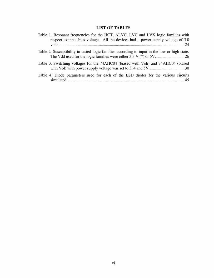
LIST OF TABLES
Table 1. Resonant frequencies for the HCT, ALVC, LVC and LVX logic families with
respect to input bias voltage. All the devices had a power supply voltage of 3.0
volts.............................................................................................................................24
Table 2. Susceptibility in tested logic families according to input in the low or high state.
The Vdd used for the logic families were either 3.3 V (*) or 5V.............................26
Table 3. Switching voltages for the 74AHC04 (biased with Voh) and 74AHC04 (biased
with Vol) with power supply voltage was set to 3, 4 and 5V. ..................................30
Table 4. Diode parameters used for each of the ESD diodes for the various circuits
simulated.....................................................................................................................45

vii
LIST OF FIGURES
Figure 1. CMOS inverter layout showing the external and internal bonding pads, bonding
wires, ESD diodes, and single stage CMOS inverter. Notice the difference in size
of the NMOS/PMOS ESD protection structures and the designed CMOS inverter.
The bonding wires were added in as a visual aid and may not be to scale [13].........7
Figure 2. Four examples of ESD protection circuit topologies: (a) ground to signal ESD
diode, (b) diffused resistance and signal to Vdd ESD diode, (c) gate grounded
NMOS and PMOS, and (d) zener topology with two diodes from ground to signal
separated by a diffused resistor and back to back zeners from signal to Vdd............7
Figure 3. Diode representations: (a) block diagram, (b) reversed-biased lumped element
model, and (c) forward-biased model..........................................................................8
Figure 4. Detected voltages for (a) a diode versus RF amplitude for several values of
saturation current and Rload = 1MΩ, and (b) with respect to 1/ Rload for a diode with
a saturation current of 1 nA and Vrf of 0.2, 0.5, 1.0 and 1.5 volts. ...........................10
Figure 5. Power Spectrum of (a) single tone RF with frequency ω0, (b) rectified RF CW,
(c) rectified RF with AM modulation frequency ωm , and (d) rectified pulse
modulated RF. Only the main lobe of the sinc function was used in (d) for
simplicity. ...................................................................................................................12
Figure 6. A comparison plot of the voltage dependent capacitances showing variation as a
function of bias voltages for an ESD diode from ground to the signal line (Lower
Diode) and an ESD diode from the signal line to Vdd (Upper Diode). The diodes
were assumed to be matched with ϕbi = 0.7 volts and n = 0.5. .................................13
Figure 7. A plot of the forward biased charge conservation capacitance (blue) with respect
to diode voltage compared to the ideal diode junction capacitance (red) and the
diffusion capacitance (black) [16]. ............................................................................14
Figure 8. Cross section of CMOS structure showing diode structures formed by p-n
junctions, the p-n associated capacitances, and the resistances due to doping of the
intrinsic substrate........................................................................................................15
Figure 9. Equivalent representation of a CMOS inverter: (a) block diagram representation
and (b) circuit diagram. ..............................................................................................16
Figure 10. A block diagram of a device under test with input and output inverter buffer
stages...........................................................................................................................17
Figure 11. Block diagram for injection testing, including bias-tee and blow-up of device
under test as a buffered inverter with ESD components. ..........................................19
Figure 12. Block diagram for injection testing, incorporating a power coupler and replacing
the bias-tee with a high-pass filter and a low-pass filter. ..........................................21
Figure 13. Block diagram of the locations of measurements taken on a HP4145B
Semiconductor Parameter Analyzer to measure the I-V characteristics of the ESD
protection devices.......................................................................................................22

viii
Figure 14. I-V characteristics of input and output ESD protection circuits for 74HCT04.
Measurements were taken between ground and the input signal line (ground_input),
between the ground and output signal line (ground_output), between the input
signal line and the power supply line (input_vdd), and between the output signal
line and the power supply line (output_vdd). ............................................................22
Figure 15. Input impedance of 74LVC04 in (a) magnitude and (b) phase with respect to
frequency and input bias voltages from 0.0 to 2.5 volts in 0.5 volt increments.......23
Figure 16. A plot showing the I-V characteristics of the lower ESD diode in a LVX CMOS
inverter. The data points were fit with the curve generated using Eq. (1) to
determine the saturation current (Is) and ideality factor (n). ....................................25
Figure 17. the input capacitance parameters of the p-n junction of the lower ESD protection
circuit in a LVX CMOS inverter ...............................................................................25
Figure 18. RF power level threshold required to cause state change in 74HCT04 with input
biased at Vol (Vin = 0.4 V, in blue) and Voh (Vin = 2.4 V, in red). The RF pulse
had a pulse width of 100ns and PRI of 1.0 ms for all frequencies. ..........................28
Figure 19. RF threshold power to cause a state change in 74HCT04 with various values of
Vdd. The RF pulse had a pulse width of 100ns and PRI of 1.0 ms for all
frequencies..................................................................................................................29
Figure 20. RF Power threshold to cause state change in 74HCT04 with varying Vbias
(f=1.2GHz PW=100ns PRI=10ms). Input state was set to Vol. ..............................30
Figure 21. Peak RF power of pulse modulated signal (f=1.5 GHz, PW=100ns,
PRI=10.0ms) required to cause a state change in a 74AHCT04 with increasing bias
towards switching voltage. Input state was set to Vol. ............................................30
Figure 22. Peak RF power of pulse modulated signal (f=1.5 GHz, PW=100ns,
PRI=10.0ms) required to cause a state change in a 74AHC04 with increasing bias
towards switching voltage. Input state was set to Voh. ...........................................31
Figure 23. The measured rectified voltages for the LVC, LVX, HCT and VHC CMOS
inverters. The RF amplitude was kept constant at 2V. ............................................31
Figure 24. The DC output voltage and DC power supply current of 74HCT04 CMOS
inverter due to RF signal with a frequency of the input impedance resonance
injected for (a) a low bias of 0.5 V and (b) a high bias of 2.0 V. .............................32
Figure 25. The DC output voltage and DC power supply current of 74LVX04 CMOS
inverter due to RF signal with a frequency of the input impedance resonance
injected for (a) a low bias of 0.5 V and (b) a high bias of 2.0 V. .............................32
Figure 26. RF gain and output voltage due to RF signal with a frequency of the input
impedance resonance for HCT CMOS inverter when the input had a (a) low bias
level of 0.5 V and a (b) high bias level of 2.0 V. ......................................................34
Figure 27. RF gain and output voltage due to RF signal with a frequency of the input
impedance resonance for LVX CMOS inverter when the input had a (a) low bias
level of 0.5 V and a (b) high bias level of 2.0 V. ......................................................35

ix
Figure 28. Time domain plot for RF injection experiment on a 74HCT04 inverter
corresponding time delays between leading edge of the RF pulse envelope (f0 = 3.8
GHz, PW = 100 ns, PRI = 10.0ms) and output voltage (a), trailing edge of the RF
pulse envelope and output voltage (b) and pulse width of the output voltage pulse
(c). ...............................................................................................................................37
Figure 29. Delay times between the envelope of the injected RF signal and the voltage
change at the output. Increasing in RF power leads to a decrease in the leading
edge delay (red), an increase in the trailing edge delay (greed), and the output
voltage pulse width (blue) exceeding the pulse width of the injected RF signal
(black). ........................................................................................................................37
Figure 30. Output voltage and power supply current change in a 74HC04 with applied RF
pulses (f=2.4 GHz, PW=100ns, PRI=10.0ms) for Vdd=3,4, and 5 volts. ................39
Figure 31. Results of pulsed RF (pulse width = 3 µs, PRI = 100 µs, peak power level =
12.25 dBm) injection into a 74ALVC04 inverter. The upper left plot displays the
RF injected power level and pulse width. The upper right plots are the measured
induced rectified voltage at the input. The lower left plot is the low frequency
output voltage. The lower right plot displays the frequency spectrum of the signal
detected at the output..................................................................................................40
Figure 32. Results of pulsed RF (pulse width = 3 us, PRI = 100 us, peak power level = 16.0
dBm) injection into a 74ALVC04 inverter. The upper left plot displays the RF
injected power level and pulse width. The upper right plots are the measured
induced rectified voltage at the input. The lower left plot is the low frequency
output voltage. The lower right plot displays the frequency spectrum of the signal
detected at the output..................................................................................................40
Figure 33. Results of pulsed RF (pulse width = 3 us, PRI = 100 us, peak power level = 21.0
dBm) injection into a 74ALVC04 inverter. The upper left plot displays the RF
injected power level and pulse width. The upper right plots are the measured
induced rectified voltage at the input. The lower left plot is the low frequency
output voltage. The lower right plot displays the frequency spectrum of the signal
detected at the output..................................................................................................42
Figure 34. Results of pulsed RF (pulse width = 3 us, PRI = 100 us, peak power level =
24.75 dBm) injection into a 74ALVC04 inverter. The upper left plot displays the
RF injected power level and pulse width. The upper right plots are the measured
induced rectified voltage at the input. The lower left plot is the low frequency
output voltage. The lower right plot displays the frequency spectrum of the signal
detected at the output..................................................................................................42
Figure 35. A simulation showing resonances caused by using (a) a simple circuit with an
inductor and capacitor in series creating and (b) the resulting impedance. The
capacitor Cj was varied over the values 6 pF (green), 7 pF (red), 8 pF (purple), 9 pF
(yellow), and 10 pF (magenta) to create a change in the resonance frequency of 200
MHz (compare with the measured results in Figure 15)..........................................46
Figure 36. (a) A comparison plot of the voltage dependent capacitances showing variation
as a function of bias voltages for an ESD diode from ground to the signal line

x
(Lower Diode) and an ESD diode from the signal line to Vdd (Upper Diode). The
diodes were assumed to be matched with ϕbi = 0.7 volts and n = 0.5. (b) A plot of
the change in the resonant frequency of upper and lower diodes with Cj0 = 3.5 pF
and L = 7 nH...............................................................................................................47
Figure 37. (a) A plot showing the comparison of the input impedance of a 74ALVC04
circuit measurements to the results of the simulation circuit in (b). The measured
data for the input bias voltage of 0.0 and 2.0 volts are red and blue, respectively,
and the calculate impedance form the simulation are purple and green for bias
voltages of 0.0 and 2.0 volts, respectively.................................................................48
Figure 38. (a) RF to DC drive curve and (b) PSPICE circuit used to match simulation
results with measurements for the LVX inverter. .....................................................49
Figure 39. The circuit diagram of the CMOS inverter circuit with a single ESD diode used
to simulate rectification effects in the time domain . ................................................50
Figure 40. Plots showing the effects of rectification showing the voltage at the (a) input and
(b) output for RF voltages of 0.5, 1.0 and 1.5 V. ......................................................51
Figure 41. Comparison of the effects an injected RF signal at (a) the input of a model and
(b) the output of the first stage of an ALVC circuit. The top picture is of the RF
signal (blue) and the mean of the RF pulse (red) as seen through a low-pass filter.
The lower picture uses the mean of the RF signal as stimulus (blue) and also shows
the mean as seen through a low-pass filter (red). ......................................................53
Figure 42. Comparison of the effects an injected RF signal at (a) the output of the second
stage and (b) the output of the inverter of an ALVC circuit. The top picture is of
the RF signal (blue) and the mean of the RF pulse (red) as seen through a low-pass
filter. The lower picture uses the mean of the RF signal as stimulus (blue) and also
shows the mean as seen through a low-pass filter (red)............................................53
Figure 43. Circuit diagram for the waveforms with RF stimulus in Figure 41 and Figure 42.
The circuit diagram for the DC waveforms is similar but replaced the RF source
with a file input source. ..............................................................................................54
Figure 44. Output voltages of the SPICE circuit model in Figure 43, which show for most
RF voltages the device going into hard conduction after the RF pulse. The RF pulse
is varied in amplitude from 2.0 to 3.75 volts in 0.25 volt increments. The RF had a
center frequency of 1.0 GHz, and a pulse width of 150 ns and was delayed by 10 ns.54
Figure 45. The AC gain between the first stage, second stage, third stage, and the entire
CMOS inverter for (a) low logic state (vbias = 0.5 volts) and (b) high logic state
(vbias = 2.5 volts).......................................................................................................56
Figure 46. PSPICE circuit of LVC CMOS inverter, which simulated relaxation oscillations
as seen in Figure 47....................................................................................................57
Figure 47. PSPICE simulation output of a LVC type of circuit showing the induced RF at
the input with relaxation oscillations and a bias shift at the output including
relaxation oscillations and latent latching..................................................................57

xi
Figure 48. MOSIS chip designed to test S-parameters of ESD structures and to use in RF
injection experiments. ................................................................................................62

xii
LIST OF ABBREVIATIONS AND DEFINITIONS
C – capacitance
CAS – column address strobe
COTS – commercial off the shelf
DF – duty factor (pulse width/PRI)
DUT – device under test
EMC – electromagnetic compatibility
EMI – electromagnetic interference
ESD – electrostatic discharge
f0 – center frequency, or injected RF signal frequency
fT – transition frequency, or crossover frequency
ggNMOS – gate grounded n-doped MOSFET
HPM – high power microwave
IC – integrated circuit
L – inductance
MOSFET – metal oxide semiconductor field emission transistor
PRF – pulse repetition frequency (1/PRI)
PRI – pulse repetition interval (1/PRF)
PW – pulse width
R – resistance
RAS – row address strobe
RF – radio frequency
RFI – radio frequency interference
S-parameters – scattering parameters
Vdd – device power supply voltage
VNA –Vector Network Analyzer
Vsp – CMOS Inverter Switching Point Voltage

1
CHAPTER 1 INTRODUCTION
The effects of electromagnetic interference on electronics have been directly
attributed to the RF signal or to the rectification of modulated RF signals. Previous work in
RF injection experiments has examined the propagation delays, logic state changes and
latch-up due to the RF signal for frequencies below the transition frequency (fT) of the
circuit tested. Above the transition frequency of circuits, errors have been associated with
the induced low-frequency voltages due to the rectification effects of the RF. Although
rectification has been observed in discrete transistors at microwave frequencies, the most
susceptible components in more complex logic circuits have not been identified.
1.1. Background
The literature on experiments examining the effects on EMI on electronics have
been found to focus on two different frequency ranges: the regions below and above the
rolloff frequency of the circuits under test. In these earlier cases, test frequencies were kept
under 800 MHz. This range is where the RF had a direct effect on the circuit. And above
800 MHZ, the rectification of RF signal was observed to have more of an impact on
causing effects in circuits. A brief summary of these studies is provided below to give an
idea of the effects observed and the ideas each of the studies proposed as potential
problems.
In 1985, Tront injected CW RF signals at frequencies of 100 and 220 MHz into the
junction between a NMOS driver stage and a NMOS buffer stage while simultaneously
stimulating the driver circuit with logic. The effects observed included the logic pulses
changing state, logic pulse propagation delay, and circuit latch-up [1]. This research
investigated state changes and other effects due to the direct influence of the RF signal, and
showed how the relationship of the phase of the RF signal could affect the propagation of
logic pulses through digital logic circuits. Laurin examined the effects of inverters by
direct injection between CMOS inverter stages and on crystal oscillators [2]. The devices
tested were CD4007A inverters arranged in a series to simulate a realistic logic circuit
environment using a coupling capacitor soldered in between two inverters to inject RF
signals. The direct injection experiments used RF frequencies of 5, 10, and 50 MHz. A

2
loop antenna was incorporated at the injection point to help the coupling of RF into the
system, used for test frequencies up to 200 MHz. Laurin noticed resonances associated
with the antenna helping to boost the amplitude of the RF signals which had greater
influence on the effects observed in his testing.
Boeing’s Integrated Circuit Electromagnetic Immunity Handbook covered the
systematic power threshold testing of various logic devices in the late 70’s with follow-up
testing in 1999 [3]. Experiments cover the frequency range of 10 MHz to 10 GHz with
power levels up to 27 dBm. Logic families tested included TTL, LS and ALS. These
rigorous experiments injected RF signals into the input, output, and power supply pins of
several types of logic devices comparing the threshold power curves for the separate cases
when the input was in the low and high logic levels. Susceptibility in the devices tended to
be below 1 GHz and at power levels above 20 dBm, indicating increasing required power
with frequency.
The effects of microwave and RF signals causing soft-errors by rectification of ??
were investigated as early as 1975 by Richardson who examined rectification by bipolar
and field-effect transistors from 1 MHz to 10 GHz [4] - [7]. Simple models for the
rectification effects were based on small signal analysis and the characteristic equations for
the transistors. Current and voltage rectification sensitivity were determined theoretically
and compared with measured results. Richardson mentions the inductance of the bonding
wires is approximately 3 nH for his circuit and MOSFET gate capacitances were measured
around 0.5 pF. Any effect of resonance due to these components would be well above the
10 GHz range.
A series of experiments performed by Kenneally looked into the effects of ESD
protection devices in MOS devices and the susceptibility of CMOS and low power
Schottky type logic circuits to injected RF signals [8] - [10]. One set of experiments
showed the partial removal of the ESD protection diodes in an 8086 microprocessor led to
an increase in the required CW power to cause state changes [8]. Kenneally pointed out the
circuits in question had rolloff frequencies around 300 MHz, below which circuits were
directly susceptible to RF signals. Kenneally mentions that above the transition frequency
(fT) of the circuits tested, the circuits tended to be susceptible to the induced rectified bias

3
shifts causing upset and timing errors [8]. Testing about 800 MHz was not performed
because of a belief that the effect of input inductance would not be a factor until 20 GHz.
1.2. Motivation for Study
Initial high frequency (300 MHZ – 2 GHz) testing we performed on computer
DRAM memory modules showed RF rectification was induced at the injection points.
With increasing power memory, bit errors were detected as well as periodic computer
failures depending on frequency and power levels. Measured threshold power levels for
CW and pulse modulated RF signals with a duty factor of 50 % showed a difference
between 7 and 10 dB in peak power to cause effects. These tests agreed with those
previously found in the literature, pointing to the rectification effects being effective at
causing errors in digital electronics. A short discussion on the DRAM memory experiments
is provided in Appendix A.
This testing led to interest in performing experiments on the basic logic circuit
building blocks to determine why modulated high frequency RF signals had more effect on
the DRAM than in the CW case. We were interested in creating a controlled environment
to eliminate the complexities of larger systems, however, having the most basic circuitry
found in modern electronics. Although several types of discrete circuits have been
previously determined to rectify RF, no candidates have been proposed and proven to be
the most sensitive to rectification in integrated circuits.
We also wanted to use low duty factor pulse modulated RF to eliminate thermal
effects in the devices. Previous studies also tended to focus only on the threshold power
levels of high frequency signals to cause effects. This is partially due to the limitations of
the equipment at the time including the sampling rates and abilities of available
oscilloscopes. Of interest in this study are the reproducible effects that can be caused by
low-power RF pulses on electronics, attempting to discover all of the induced behaviors
within the circuits and being able to model these effects.
1.3. Organization of Thesis
This thesis focuses on the rectification properties of the input ESD protection circuit
and the effects of resonances found at the inputs of CMOS inverters. Several logic families
4
of CMOS inverters from different manufacturers have been tested to observe and measured
the various effects of RF on the circuits and in order to determine the sources of these
effects. The goal was to perform very thorough experiments, in depth research of circuit
components, and the building of computer models to reproduce the effects observed in our
measurements.
Chapter 2 will introduce the fundamental circuits that make up the input circuitry to
the CMOS inverter. ESD protection devices are briefly discussed covering different
topologies common in modern electronics. The basic equations for the diode were used to
determine the parameters, which affect rectification sensitivity an RF signal to cause state
changes in digital electronics. Equations based on the operation of the CMOS inverters
show insight into the parameters required to cause the inverter to switch.
The results of the measurements used to determine effects and their sources are
covered in Chapter 3. Input port characteristics will give insights into the mechanisms
dominant to DC and AC stimulus. These measurements were intended to be the basis in
building computer models. Power threshold experiments were used to determine the
differences in susceptibilities of different input logic states as well as to other circuits.
Finally, the results of simulations in comparison to measured effects are covered in
Chapter 4. Models designed from the parameters extracted in the previous section were
simulated to match results to the observed measurements.

5
CHAPTER 2 HIGH SPEED CIRCUIT CHARACTERISTICS
2.1. Introduction
The two main fundamental structures of CMOS inverters are the ESD protection
devices, located at the input and output ports of the device, and the inverter itself. ESD
protection device topologies differ with almost every different class of logic family
available. However, each one of these topologies contains at least one p-n junction, which
is the fundamental physical component of a diode. The following sections will focus on the
various topologies of ESD protection devices, the basic equations of the ideal diode, and
the characteristic equations for the CMOS inverter.
2.2. ESD Protection Device Topologies
Electrostatic discharge (ESD) was recognized as a potential threat to circuits early
in the development of digital electronics. Potential differences between chips and insertion
devices (human hands and insertion machines) pose as sources for a possible discharge
event, which could destroy a circuit before it is even integrated into the destined circuit.
Gate oxides can break down with an applied electric field less than 6MV/cm, amounting to
6 V across a gate 10 nm thick oxide [11]. ESD protection devices have been nominally
integrated into the input and output ports of all digital devices in order to source or sink
current away from the gate oxide during an ESD event.
ESD protection device topologies differ from one logic family to the next and vary
with every manufacturer. These devices may contain a single diode, several stages of
diodes, in-line resistances to suppress current spikes, or more advanced components such
as thick field oxide devices or silicon controlled rectifiers. Although the ESD topologies
differ with logic families, the same topologies are normally used within a given logic
family [12].
ESD protection devices are placed into two different classifications defined by
operation, breakdown and non-breakdown. The non-breakdown components, such as
diodes, BJTs and MOSFETs, operate near normal operating parameters, are well
understood and the easiest to model. One disadvantage to non-breakdown ESD

6
components is the size of the device, which can be orders of magnitude larger to the
circuits they protect as seen in Figure 1 that shows the layout of the ESD protection diodes,
bonding wires, CMOS inverter, power supply bus, and ground bus [13].
Manufacturer’s datasheets containing block diagrams of the ESD devices found in
the circuits tend to use very basic circuits to signify the basic functionality of the protection
used. Examples of commonly found ESD protection topologies are shown in Figure 2,
demonstrating single diode structures with and without diffusion resistors, gate grounded
NMOS (ggNMOS) and the PMOS equivalent, and a topology using Zener diodes.
Breakdown devices do not normally work in normal operation of the semiconductor
and are designed to handle extreme ESD events. These devices are much harder to model,
but are more area efficient. The main mechanisms of these devices are reverse avalanche
breakdown or a forward snap-back voltage breakdown. The breakdown devices include
[14]:
− Thick Field Oxide (TFO)
− Zener Diodes
− Grounded Gate NMOS (ggNMOS)
− Silicon Controlled Rectifier (SCR)
− PIPE (punch through-induced protection element)
− LVSCR (low voltage SCR)
− GCNMOS (gate-coupled NMOS)
− Bimodal SCR
− Spark Gap
All of these devices realized in semiconductors contain at least one p-n junction.
Even though the non-breakdown devices may operate in a region outside of normal
operation in the case when an ESD event occurs, they will operate as predicted in normal
operating regimes (for example, a Zener is sometimes used for its reverse breakdown
characteristics, however, it will operate like a normal diode in its forward biased region).
In normal CMOS operation after the device has been installed into the destination
circuit, ESD events are not expected to occur and the ESD protection devices are
electrically turned off or reverse biased.

7
Figure 1. CMOS inverter layout showing the external and internal bonding
pads, bonding wires, ESD diodes, and single stage CMOS inverter. Notice the
difference in size of the NMOS/PMOS ESD protection structures and the
designed CMOS inverter. The bonding wires were added in as a visual aid and
may not be to scale [13].
Figure 2. Four examples of ESD protection circuit topologies: (a) ground to
signal ESD diode, (b) diffused resistance and signal to Vdd ESD diode, (c) gate
grounded NMOS and PMOS, and (d) zener topology with two diodes from
ground to signal separated by a diffused resistor and back to back zeners from
signal to Vdd.
2.3. Diode Characteristics
A diode is formed when layers of p-doped and n-doped semiconductor are
fabricated next to each other creating a potential difference between the two layers.
Although there are various different types of diodes (p-n, p-i-n, Schottky, Zener, tunneling,

8
etc), only the p-n diode will be considered in this discussion. In order to allow current to
flow through the device, a positive voltage must be applied across the p-side (anode) and
the n-side (cathode) in order to offset the potential barrier. The voltage to activate the diode
may be DC or AC. When AC is applied to the terminals of the diode, the AC signal is
clipped or “rectified”, since only one polarity of the AC, if large enough to offset the
internal potential, will cause the diode to allow current to flow. Diodes have been used to
rectify RF in order to “detect” the signal in high frequency circuit measurements.
Detection of an RF signal is due to the non-linear effects of the diode, rectifying the RF and
converting the RF signal into DC and low frequency components.
Figure 3. Diode representations: (a) block diagram, (b) reversed-biased lumped
element model, and (c) forward-biased model.
2.3.1. Ideal Diode Equations
The current through the diode can be modeled by described by the relationship
between the current and applied voltage in the ideal diode current equation:
( ) ( 1)dV
nVts
I V I e = − (1)
where Is is the saturation current, Vd is the voltage difference across the cathode and anode
of the diode, n is an ideality factor, and Vt is the thermal voltage. The thermal voltage is
defined as kT/q where k is Boltzmann’s constant, T is temperature, and q is the charge of an
electron (Vt is approximately 26 mV at T = 300K) [15].

9
After applying a small amplitude AC signal to the continuous wave RF signal that
has specified amplitude and frequency and with the addition of a DC voltage, the applied
diode voltage and current are described as:
0 cos( )d rf rf
V V v tω= + (2)
where V0 is a DC voltage, vrf is the amplitude of a sinusoidal signal, and ωrf is the frequency
of the RF signal. Using Taylor’s expansion, the small-signal approximation for the diode
current is:
( )
2
0 0 0 0
cos( )( ) cos( ) ' ( )
2
rf rf
d rf rf rf rf
v tI V I i I v t G G O v
ωω= + = + + + (3)
with the conductance being defined as
00
( )1 s
v t
I IG
R V
+= = 0
0 't
GG
V= (4)
where I0 is the DC current component due to V0, irf is the AC current, Rv is the video
resistance, and O(vrf ) represents higher order terms [15]. Reducing the second order term
in Eq. (3), the new DC current term will create a voltage across the resistance looking out
from the cathode of the diode (Rload) in parallel with the diode video voltage:
2
2( )
4
rf s
det load v
t
v IV R R
V= (5)
where Vdet is the induced detected DC voltage and Rload is the low-frequency resistance as
seen from the input of the CMOS inverter. In Figure 4(a), detected voltages for saturation
currents between 1nA and 10 nA for a load resistance of 1 MΩ show rectified voltages for
RF amplitudes up to 1 V. The relation between the detected voltage and 1/Rload for a
saturation current of 1 nA and RF amplitudes of 0.2, 0.5, 1.0 and 1.5 volts is shown in
Figure 4(b). This last relation is important when logic devices such as tri-state buffers,
which vary between a low to high output impedance depending on state of operation, are
used in ICs.

10
(a) (b)
Figure 4. Detected voltages for (a) a diode versus RF amplitude for several
values of saturation current and Rload = 1MΩ, and (b) with respect to 1/ Rload for
a diode with a saturation current of 1 nA and Vrf of 0.2, 0.5, 1.0 and 1.5 volts.
2.3.2. Bandwidth Considerations
The previous equations assumed the RF signal is continuous, and therefore
producing a purely DC voltage term. However, in the case where the RF is modulated, the
‘DC’ voltage will have frequency components associated with modulation of the RF signal.
The required bandwidth to view the signal can be determined by starting with a
Fourier transform on the cosine function:
0 0
1( ) [ ( - ) ( )]
2X f f f f fδ δ= + + (6)
where f = ω/2π and f0 = ω0/2π [16]. Although the transform contains negative frequency
components, only the positive frequency components will be displayed on a spectrum
analyzer (Figure 5a,b).
Modulation is often used with RF signals and comes in different forms including
some of the more common types: amplitude (AM), frequency (FM) and pulse modulation.
In the case of amplitude modulation, the equation for the signal is defined as:
0 (1 cos( )) cos( )rf m o
v v m t tω ω= + (7)
where m is the modulation index (normally 0 < m < 1) and ωm is the modulation frequency.
Substituting into the small signal current portion of Eq. (4) and expanding, the AC diode
current now becomes

11
2
2 200 0 0 0 0( ) (1 cos )cos ' (1 cos ) cos
2rf m m
vi t v G m t t G m t tω ω ω ω= + + +
0 0 0 0 0[cos cos( ) cos( ) ]2 2
m m
m mv G t t tω ω ω ω ω= + + + −
2 2 2
00 0' [1 2 cos cos 2 cos 2
4 2 2m m
v m mG m t t tω ω ω+ + + + +
2
0 0 0cos(2 ) cos(2 ) cos 22
m m
mm t m t tω ω ω ω ω+ + + − +
2 2
0 0cos 2( ) cos 2( ) ]4 4
m m
m mt tω ω ω ω+ + + − (8)
which shows the frequency content of the modulated signal. An additional DC term is
added to the term found in Eq. (7), and the lower frequency components related to the
modulation frequency are now visible in the spectrum of the signal of the detected signal
(Figure 5c).
Pulse modulation can be considered to be a particular type of AM modulation. By
using the step function as the simplest model for pulse modulation and using the
‘multiplication theorem’ for Fourier transforms, the time domain function and Fourier
Transform pairs (the time domain and the frequency domain equations) for the pulse
modulate RF signal are given as:
0( ) ( , ) cos(2 )x t u t f tτ π= (9)
0 0 0( ) sinc( ) [ ( - ) ( )] 2
X f f f f f fτ
τ δ δ= + + (10)
where u(τ,t) is a step function with τ as the pulse width and t is time. The frequency
spectrum of the pulse modulated RF signal with AM modulation would look similar to the
CW RF signal with AM modulation with sinc functions of determinable width replacing
the delta functions at the same frequencies as found in Eq. (10) and shown in Figure 5(d).
The Fourier transform of the pulse modulation case is important in determining the
bandwidth required for the input signal and will be discussed in Chapter 3. As a sample
calculation, the required frequency bandwidth required to detect the envelope of the pulse-
modulated RF with a pulse width of 100 ns will be f = 1/100ns = 10MHz. The previous
calculation was for an idealized pulse, albeit in normal pulse modulation, the envelope has

12
Figure 5. Power Spectrum of (a) single tone RF with frequency ω0, (b) rectified
RF CW, (c) rectified RF with AM modulation frequency ωm , and (d) rectified
pulse modulated RF. Only the main lobe of the sinc function was used in (d)
for simplicity.
a finite rise and fall time which will have higher frequency components in the Fourier
spectrum and measurement equipment will require additional bandwidth to detect the
signal.
2.3.3. Capacitance Model
Returning to the model in Figure 3, the depletion region formed between the p-n
layer of the diode is modeled by a voltage dependant capacitance. The capacitance is
commonly referred to as the junction capacitance and is modeled as:
0
1
j
j m
d
bi
CC
V
ϕ
=
+
(11)
where Vd is the applied reverse biased voltage, Cjo is the junction capacitance when Vd = 0,
ϕbi is the built-in junction potential, and m is the emission coefficient.

13
If a bias voltage is swept over the ESD topologies in Figure 2(a) and (b), excluding
inline resistances, the reverse biased capacitances will decrease with increasing voltage
Figure 6. A comparison plot of the voltage dependent capacitances showing
variation as a function of bias voltages for an ESD diode from ground to the
signal line (Lower Diode) and an ESD diode from the signal line to Vdd (Upper
Diode). The diodes were assumed to be matched with ϕbi = 0.7 volts and n =
0.5.
across the diode. For the lower diode (from ground to the signal line), the change from a
low logic state bias to a high bias state will decrease the capacitance as it follows Eq. (11).
The junction capacitance in the diode from the signal line to Vdd will decrease capacitance
as the bias level goes from high to low, taking into account the diode voltage is now equal
to Vdd minus the voltage on the signal line. A comparison of the normalized capacitance
changes due to a bias voltage sweep from 0 to 3 volts for the diodes in the previously
mentioned configurations is shown in Figure 6 for ϕbi = 0.7 volts and n = 0.5. The change
in capacitance in the case of n = 0.5 for a 3 volt change is 42.6% from the zero bias
capacitance.
The reverse bias conditions and equations are dominated by the flow of the majority
carriers. The diode model can be modified to include the effects of the minority carriers as
the diode is forward biased. As a diode becomes forward biased, minority carriers
accumulate in the neutral regions adjacent to the depletion region. The movements of these
charges create an effective diffusion capacitance (CD) and conductance (GD). The addition
of the diffusion capacitance to the junction capacitance increase very quickly as the voltage
becomes forward biased Figure 7.

14
The capacitance and conductance associated with the minority carrier oscillations
are frequency dependent because of the supply and removal of minority carriers is not as
rapid as that of majority carriers. Because of this the minority carriers have difficulty
staying in sync with the AC signal, thus making the conductance and capacitance both
frequency dependent. The equations for the diffusion conductance and capacitance are:
1
2 20 2( 1 1)2
D p
GG ω τ= + + (12)
1
2 20 2( 1 1)2
D p
GC ω τ
ω= + − (13)
where ω is the angular frequency of a signal applied to the diode, and τp is the minority
charge absorption time constant [17].
Figure 7. A plot of the forward biased charge conservation capacitance (blue)
with respect to diode voltage compared to the ideal diode junction capacitance
(red) and the diffusion capacitance (black) [16].

15
2.4. CMOS Inverter Characteristics
Metal oxide semiconductor field effect transistors (MOSFETs) are classified as
NMOS (the source and drain regions of the resistor are heavily doped with n-type material)
or PMOS devices (the source and drain regions are heavily doped in p-type material). A
Complimentary Metal Oxide Semiconductor (CMOS) device is a combination of NMOS
and PMOS transistors in series (Figure 8). CMOS devices have become a popular choice
in every area of digital circuit design because of the low current consumption, reduction of
size, reduction of operation voltages, and large noise immunity.
The basic building block in CMOS digital logic devices is the inverter. In inverter
CMOS circuits, the drains of the NMOS and PMOS devices are connected together, the
gates are connected together, and the source and substrate are connected to ground and Vdd
for NMOS and PMOS, respectively (Figure 9). Logic topologies use the inverter in
different series and parallel configurations, but for ease of analysis, a single inverter stage
will be analyzed in this section.
Figure 8. Cross section of CMOS structure showing diode structures formed by
p-n junctions, the p-n associated capacitances, and the resistances due to doping
of the intrinsic substrate.
The inverter works from applying a voltage to the input of the device which will
cause the NMOS device to turn on when the input voltage is high. The ‘switching point’ is
the voltage when the output of the voltage changes from one state to another (high to low

16
or low to high). This voltage is dependent on Vdd, device size, and threshold voltages for
the NMOS and PMOS devices, and is defined as
( )
1
nTHN DD THP
p
sp
n
p
V V V
V
β
β
β
β
+ −
=
+
(14)
where VTHN is the threshold voltage for the NMOS device, VTHP is the threshold voltage for
Figure 9. Equivalent representation of a CMOS inverter: (a) block diagram
representation and (b) circuit diagram.
the PMOS device, and VDD is the power supply voltage. The size characteristics of the
MOS structures are included in βn and βp and defined as:
nn n ox
n
WC
Lβ µ=
p
p p ox
p
WC
Lβ µ= (15)
where µn and µp are the mobility of the minority carriers in the n- and p- doped
concentrated regions, respectively, Cox is the capacitance of the gate oxide, Wn, Ln, Wp, and
Lp are the gate widths and lengths of the NMOS and PMOS devices, respectively [18].
If the devices have equal threshold voltages and have physical dimensions and
mobility such that βn = βp, then the switching voltage will be equal to Vdd/2. In most
devices, this is not the case, where it is difficult to determine the mobility of the NMOS and
PMOS devices which is directly proportional to doping levels, and then to scale the
dimensions for the mobility offset.

17
With advancements in circuit design today, additional circuitry is designed to
improve noise immunity, to offset the switching voltage and in some cases give the circuit
a hysteresis in the switching voltage as in Schmidt Trigger devices. Also for increasing the
signal to noise ratio and noise rejection of the circuit, input and output buffer stages are
usually added to a circuit [19]. Buffer stages are common in every type of digital logic
circuit and one buffer stage is normally a single inverter stage (Figure 10).
Based on the information on CD4xxxB Series logic devices, buffered gates offer a
large noise margin, constant output impedance, large AC gain, lower input capacitance,
while the unbuffered have faster propagation delay, larger AC bandwidth and are not
susceptible to output oscillations [19]. The buffer stages provide large DC gain between
stages leading to defined transition voltages and faster transition times.
Output oscillations have been observed in buffered logic devices when a slow rising
voltage is applied to the input of the circuit, where this effect was not observed in circuits
that were unbuffered. Logic manufacturers set limitations on the edge characteristics of
logic pulses to prevent excitation of these oscillations.
Figure 10. A block diagram of a device under test with input and
output inverter buffer stages.
Another method of preventing undesired noise is by using more complex topologies
such as “bus hold circuitry” and Schmitt triggers which use additional MOSFET stages to
provide feedback to input stages to clamp them to desired logic state [20]. Although all of
these types of additional circuitry exist and are implemented in a large majority of the
devices tested they will not be considered in the following analysis and simulations.
Simple models of CMOS inverters will be considered including buffer stages and ESD
topologies based on datasheets found on the logic circuits.

18
CHAPTER 3 RF INJECTION EXPERIMENTS
3.1. Introduction
Direct injection and irradiation experiments are the two types of experiments
commonly used for determining the effects of electromagnetic radiation in electronics.
Direct injection experiments have the advantage of being able to couple the most power
into a specific point in a circuit, to exactly know how much power is incident to the device
under test, but has the disadvantage of creating a fictitious circuit environment to determine
the effects. Irradiation experiments have the advantage of not altering the circuit under test
and keeping the integrity of the circuit testing environment as ideal as possible. The
disadvantages to irradiation include the requirement for higher power levels, antenna
patterns changing with frequency, near-field ambiguities, and difficulties in calculating the
exact amount of power incident to a circuit or transmission line.
Direct injection experiments were chosen to determine exactly how much power
was required to cause an effect in the DUT. This method can be used to measure precisely
how much power is incident to, reflected from and transmitted into the DUT. By using a
power coupler, the incident and reflected RF power is measured and the transmitted power
calculated from these values. However, this setup can incorporate an unrealistic circuit
environment due to loading effects at the injection point.
3.1.1. Experimental Setup
The equipment setup for the injection experiments followed the basic construction
demonstrated in the block diagram of Figure 11 with an RF source fed into an amplifier
leading to a bias-tee circuit coupled into the input of the DUT. An oscilloscope was used to
measure the induced voltages at the input in between the RF choke of the bias-tee and a
pull-up resistor. The output was loaded by a load resistor which was used to measure
changes in the output voltage by an oscilloscope or to determine RF feedthrough by a
spectrum analyzer. Because of the variety of experiments performed, the following
sections will indicate the specific equipment used for measurement of interest. One
consideration to take into account when performing RF injections experiments is the effect

19
the measuring equipment has on the operation of the circuit and in the measurements
themselves.
Figure 11. Block diagram for injection testing, including bias-tee and blow-up
of device under test as a buffered inverter with ESD components.
3.1.2. Loading Effects on the input circuit
Loading problems arise from introducing a direct injection point into a circuit. In
an ideal RF injection situation, the circuit under test would be operating under normal
circumstances, being a circuit in a series or parallel with other circuits, with RF coupled
into the input of the circuit with no change in normal performance of the digital device due
to the RF transmission line. In previous direct injection experiments [1]-[10], a bias-tee or
a DC-blocking capacitor was used for electromagnetic coupling (Figure 11). In these two
cases, the electromagnetic signals were capacitively coupled into the input of the DUT to
determine effects.
The coupling capacitor and the impedance of the RF injection transmission line
create a single-pole, high-pass filter. If the induced signal at the input of the circuit
contains frequency components, which are above the cutoff frequency of the high pass
filter, the signal can shunt through the capacitor and be loaded down by the RF
transmission line. However, using too small of a value for a capacitor could result in an AC

20
voltage divider between the coupling capacitor and the capacitance of the ESD protection
circuits and the input capacitance of the CMOS inverter.
A high-pass filter (HPF) may be used to couple the RF into input of the circuit
reducing the loading effects. By increasing the number of poles in the transfer function of
the filter (coupling capacitor), the impedance seen at the lower frequencies will be higher
and closer to an open circuit, and still pass through the RF frequencies as if it were a
matched load (Figure 12).
The DC port of a bias-tee is normally a single inductor. The inductor and the
impedance of the transmission line form a single-pole, low-pass filter (LPF). For DC
probing the input of the device, the frequency components of the input DC voltage must be
lower in frequency than the cutoff frequency of the LPF. If this is not the case, the signal
being probed will look distorted on an oscilloscope, with an inaccurate representation of the
rise time, rectified voltage level, pulse width and the fall time of the induced voltage pulse.
One way to avoid the loading problems of the bias-tee is to replace it with multi-
pole, high-pass and low-pass filters (Figure 12). A high-pass filter with a higher corner
frequency than the single capacitor filter and a much steeper roll-off will match the line at
RF frequencies, and act like a high impedance transmission line at lower frequencies. A
low-pass filter will require a corner frequency high enough to allow the frequency content
of the pulse envelope to be measured, while looking like a high impedance transmission
line to the RF signal.

21
Figure 12. Block diagram for injection testing, incorporating a power coupler
and replacing the bias-tee with a high-pass filter and a low-pass filter.
3.2. Measured Inverter Port Characteristics
Using an HP4145B Semiconductor Parameter Analyzer, the DC I-V measurements
were taken of the HC, HCT, AHC, and AHCT families of inverters to determine if the
inputs’ and outputs’ ESD protection showed the same diode characteristics as discussed in
Section 2.3. Four measurements were taken with the first port acting as the voltage
reference: ground to input (ground_input), input to Vdd (input_vdd), ground to output
(ground_output), and output to Vdd (output_vdd) as demonstrated in Figure 13. The
HP4145B had the upper and lower current limits set to +/- 50 µA, respectively.
The four measurements for the 74HCT04 show the I-V characteristics have
different forward and reversed biased attributes (Figure 14). The measurements
demonstrate the forward conduction region has a turn-on voltage around 0.4-0.7 volts for
the ground_input, input_vdd, and output_vdd, and a turn on voltage of 0.1 volts for
ground_output. The reverse biased voltage sweep indicated low reverse breakdown
voltages between –0.75 and –2.5 volts. The differences can be attributed to the topology of
the ESD protection device as well as to variations in manufacturing the semiconductor.
The I-V characteristics indicate p-n junctions are present at the four measurement
points, which supports the hypothesis of the ESD protection devices being the RF rectifiers.
Measurements for the 74HC04, 74AHC04, and 74AHCT04 circuits are located in
Appendix B. In certain cases such as the 74AHC04, the measurements indicated a p-n
junction was not located at a specified port.

22
Figure 13. Block diagram of the locations of measurements taken on a
HP4145B Semiconductor Parameter Analyzer to measure the I-V
characteristics of the ESD protection devices.
To determine the input impedance of the CMOS devices, an HP8722D Vector
Network Analyzer (VNA) was used to record the S11 parameters of the HCT, ALVC, LVC,
and LVX CMOS inverters. The frequency range of the VNA was set from 50 MHz to 2
GHz for all the devices. The circuits were set up without power to the Vdd pin in order to
test the characteristics of the lower ESD diode.
Since the ESD protection circuit contains a voltage dependent capacitance, we were
interested in comparing the differences between the input impedance for the low and high
logic states to determine the effects of the change in input bias voltage. A DC bias voltage
was coupled into the VNA through the bias voltage port while the frequency response was
measured for a series of input bias voltage levels. The input impedance test of LVC
demonstrates a series resonance in the impedance dependant on the bias voltage (Figure
15a). A shift in the resonant frequency between the low (red) and high (black) state is
approximately 125 MHz (Figure 15).
Figure 14. I-V characteristics of input and output ESD protection circuits for
74HCT04. Measurements were taken between ground and the input signal line
(ground_input), between the ground and output signal line (ground_output),
between the input signal line and the power supply line (input_vdd), and
between the output signal line and the power supply line (output_vdd).

23
(a)
(b)
Figure 15. Input impedance of 74LVC04 in (a) magnitude and (b) phase with
respect to frequency and input bias voltages from 0.0 to 2.5 volts in 0.5 volt
increments.
The input impedances for the other circuits tested are in Appendix D. Dips in
impedance are associated with a resonance caused by an inductance and a capacitance in

24
series. The resonant frequencies for the ALVC, HCT, LVC, and LVX are in Table 1 for
the low and high logic state voltages, and a power supply voltage of 3.0 volts.
In later injection experiments, the input resonant frequency was found to decrease
in certain circuits after the power supply was connected back up to the circuit. The change
in the resonant frequency can be explained by the influence of additional capacitances
contributed by other ESD protection components. This influence on the input resonance
frequency is discussed further in Section 4.3.1.
To determine the DC I-V characteristics of the lower ESD diode, the CMOS
inverter was setup with the power supply pin floating. A bias voltage was applied across
the ground to the signal line with an Agilent 34401A 6 ½ Digital Multimeter in series with
the power supply in order to measure the current. The input bias voltage was swept in 5
mV steps measuring the current at each interval. The I-V measurements for the LVX are
shown in Figure 16 using Eq. (1) to calculate the saturation current to be 5 pA and the
ideality factor n as 1.05.
Table 1. Resonant frequencies for the HCT, ALVC, LVC and LVX logic
families with respect to input bias voltage. All the devices had a power supply
voltage of 3.0 volts.
Low Bias High Bias
Logic Family
Voltage [V]
f0 [MHz]
Voltage [V]
f0 [MHz]
HCT 0 940 3 1080
ALVC 0 850 2 993
LVC 0 825 2.5 947
LVX 0 1350 2.5 1450

25
Figure 16. A plot showing the I-V characteristics of the lower ESD diode in a
LVX CMOS inverter. The data points were fit with the curve generated using
Eq. (1) to determine the saturation current (Is) and ideality factor (n).
The input capacitance of a CMOS inverter was calculated by using the S-
parameters as measured by the VNA. The high-frequency, small-signal impedance for
various bias voltages was measured by recording the S-parameters at each step of
increasing voltage. Again, the LVX inverter was measured with no power supply voltage
applied and the Vdd pin floating. By using the Smith chart display on the VNA, the input
was seen to be most capacitive in frequencies around 100 MHz. We wanted to measure the
impedance far away from the input resonance to determine the value of the capacitive
element without the effects of other parasitic elements influencing the measurements. The
bias voltage was limited to 1.5 volts because of the rapid change in the frequency response
due to the device beginning to conduct. A small band of frequencies was used to average
the values of the capacitance to eliminate noise and fluctuations in the measurements.
Using Eq. (11), a curve was generated to match the data points as close as possible (Figure
17) calculating Cj0 to be 3.6 pF, the built in potential to be 0.7 volts, and the emission
coefficient to be equal to 0.18. Deviations from the curve are most likely due to the effects
of the gate capacitances and the capacitance of the upper ESD diode.
Figure 17. the input capacitance parameters of the p-n junction of the lower
ESD protection circuit in a LVX CMOS inverter

26
3.3. Observed RF Injection Effects
The observed effects of the RF pulses injected into inverters varied with every logic
family, which included a full state change, partial state change (output voltage shift), state
changes with a the output voltage switched after the RF pulse width has terminated, RF
amplification, and induced oscillations. This section covers at least one example of each of
these cases with additional examples located in appendices where indicated.
Table 2. Susceptibility in tested logic families according to input in the low or
high state. The Vdd used for the logic families were either 3.3 V (*) or 5V.
Logic Family Input Biased Low Input Biased High
HC
HCT
AC
ACT
AHC
AHCT
LVC*
ALVC*
VHC*
LCX*
LVX*
3.3.1. Threshold Power Level Experiments
Threshold power levels of pulsed RF signals to cause a state change in the CMOS
inverters were measured to determine the susceptibility of the devices with sweeps in the
RF signal frequency, power supply voltage, and input bias voltage. The circuit setup for all
the circuits tested followed the block diagram in Figure 11. The equipment used for these
experiments was an HP 83731B signal generator for the RF source, an HP 83020A RF
amplifier, a Mini-Circuits ZFBT-6G bias-tee, a Tektronix TDS-620 Oscilloscope, and a
Tektronix P6243 FET probe.
27
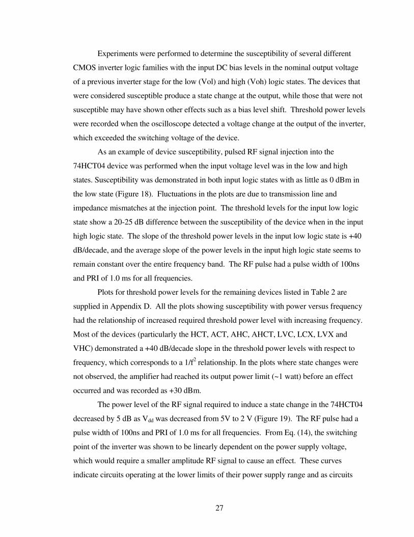
Experiments were performed to determine the susceptibility of several different
CMOS inverter logic families with the input DC bias levels in the nominal output voltage
of a previous inverter stage for the low (Vol) and high (Voh) logic states. The devices that
were considered susceptible produce a state change at the output, while those that were not
susceptible may have shown other effects such as a bias level shift. Threshold power levels
were recorded when the oscilloscope detected a voltage change at the output of the inverter,
which exceeded the switching voltage of the device.
As an example of device susceptibility, pulsed RF signal injection into the
74HCT04 device was performed when the input voltage level was in the low and high
states. Susceptibility was demonstrated in both input logic states with as little as 0 dBm in
the low state (Figure 18). Fluctuations in the plots are due to transmission line and
impedance mismatches at the injection point. The threshold levels for the input low logic
state show a 20-25 dB difference between the susceptibility of the device when in the input
high logic state. The slope of the threshold power levels in the input low logic state is +40
dB/decade, and the average slope of the power levels in the input high logic state seems to
remain constant over the entire frequency band. The RF pulse had a pulse width of 100ns
and PRI of 1.0 ms for all frequencies.
Plots for threshold power levels for the remaining devices listed in Table 2 are
supplied in Appendix D. All the plots showing susceptibility with power versus frequency
had the relationship of increased required threshold power level with increasing frequency.
Most of the devices (particularly the HCT, ACT, AHC, AHCT, LVC, LCX, LVX and
VHC) demonstrated a +40 dB/decade slope in the threshold power levels with respect to
frequency, which corresponds to a 1/f2 relationship. In the plots where state changes were
not observed, the amplifier had reached its output power limit (~1 watt) before an effect
occurred and was recorded as +30 dBm.
The power level of the RF signal required to induce a state change in the 74HCT04
decreased by 5 dB as Vdd was decreased from 5V to 2 V (Figure 19). The RF pulse had a
pulse width of 100ns and PRI of 1.0 ms for all frequencies. From Eq. (14), the switching
point of the inverter was shown to be linearly dependent on the power supply voltage,
which would require a smaller amplitude RF signal to cause an effect. These curves
indicate circuits operating at the lower limits of their power supply range and as circuits

28
powered by smaller power supply voltages, they will be much more susceptible to upset
from RF pulses.
Figure 18. RF power level threshold required to cause state change in
74HCT04 with input biased at Vol (Vin = 0.4 V, in blue) and Voh (Vin = 2.4
V, in red). The RF pulse had a pulse width of 100ns and PRI of 1.0 ms for all
frequencies.
To determine the susceptibility of the 74HCT04 inverter with respect to input bias
voltage, another set of injection experiments were performed. An RF signal with a
frequency of 1.2 GHz, pulse width of 100 ns, and PRI equal to 10 ms was injected into the
HCT inverter, recording the RF power threshold levels for different input bias voltages.
Experiments were done with the power supply voltage set to 3, 4, and 5 volts (Figure 20).
The difference in required power levels to cause a state change was on the order of 8 dB
between the cases of the power supply set to 3V and 5V.
RF threshold power levels were measured for the 74AHC04 and the 74AHCT04 for
three different power supply voltages within the operation parameters of the inverters and
while varying the input bias voltage. In the case of the 74AHC04, the device was most
susceptible when the circuit was biased in the high-logic state, and for the 74AHCT04, the
device was more susceptible when biased with a low-logic state. In each of these devices,
the switching voltage was measured for each of the power supply voltages (Table 3). The
threshold power levels were measured for different values of the input bias level and for the
power supply voltages of 3, 4 and 5 volts. The comparison of these three curves for the two

29
different devices in Figure 21 and Figure 22 for the 74AHC04 and 74AHCT04,
respectively. These plots show the amount of power required to induce the same voltage
difference for all three power supply values are identical. This implies the rectification of
the RF to induce the required voltage to cause the devices to switch is not dependent on the
power supply voltage.
Figure 19. RF threshold power to cause a state change in 74HCT04 with
various values of Vdd. The RF pulse had a pulse width of 100ns and PRI of
1.0 ms for all frequencies.

30
Figure 20. RF Power threshold to cause state change in 74HCT04 with varying
Vbias (f=1.2GHz PW=100ns PRI=10ms). Input state was set to Vol.
Table 3. Switching voltages for the 74AHC04 (biased with Voh) and 74AHC04
(biased with Vol) with power supply voltage was set to 3, 4 and 5V.
Device Vdd = 3V Vdd = 4V Vdd = 5V
74AHC04
with Voh1.4 1.9 2.4
74AHCT04
with Vol1.5 1.3 1
Switching Voltage [V]
Figure 21. Peak RF power of pulse modulated signal (f=1.5 GHz, PW=100ns,
PRI=10.0ms) required to cause a state change in a 74AHCT04 with increasing
bias towards switching voltage. Input state was set to Vol.

31
Figure 22. Peak RF power of pulse modulated signal (f=1.5 GHz, PW=100ns,
PRI=10.0ms) required to cause a state change in a 74AHC04 with increasing
bias towards switching voltage. Input state was set to Voh.
Figure 23. The measured rectified voltages for the LVC, LVX, HCT and VHC
CMOS inverters. The RF amplitude was kept constant at 2V.

32
To determine the frequency dependent rectification sensitivity for a series of logic
families, the devices were injected with a constant RF voltage of 2 volts and swept over
500 MHz to 2 GHz. Figure 23 compares the rectified voltages measured for the LVC,
LVX, HCT, and VHC CMOS inverters. In the case of the VHC, the induced voltage
exceeds the RF amplitude reaching a peak of 4 volts over the frequency range of 500 MHz
to 1.2 GHz. Similarly, the LVC device exhibits RF to DC conversions above unity from
500 MHz to 1 GHz. The HCT and LVX had transfer curves more expected of rectification,
with a RF signal to DC induced voltage conversion less than unity. The transfer curves of
the VHC and LVC devices indicate RF gain occurs within the device allowing for a larger
induced rectified envelope voltage.
(a) (b)
Figure 24. The DC output voltage and DC power supply current of 74HCT04
CMOS inverter due to RF signal with a frequency of the input impedance
resonance injected for (a) a low bias of 0.5 V and (b) a high bias of 2.0 V.
(a) (b)
Figure 25. The DC output voltage and DC power supply current of 74LVX04
CMOS inverter due to RF signal with a frequency of the input impedance
resonance injected for (a) a low bias of 0.5 V and (b) a high bias of 2.0 V.

33
Measurements of the power supply current give insight into the effects of RF on the
MOSFETs. Since the sources of the PMOS devices are all connected to the power supply
line, fluctuations in the current can indicate the time when switching occurs in the devices.
An experiment injecting RF pulses into a 74HCT04 and a 74LCX04 device biased in a low
and high logic state, showed power supply current shifts correlating to measured output
voltage changes (Figure 24 and Figure 25).
The RF frequency in this was set to the zero bias input impedance resonant
frequency of 1.35 GHz as determined in Section 3.2. The current measurements were
taken by increasing the duty factor of the pulse-modulated RF signal. Care was taken to
ensure thermal effects did not contribute to deviations in measurements of the rectified
voltage signal as power-supply current was measured. The current variations showed a
linear relationship with the changes in duty factor. The average current measurements
were divided by the duty-factor ratio to give the peak power-supply current.
Application notes on various logic families indicate these current spikes are very
common but differ in magnitude from device to device [21]-[25]. These spikes are
indicators that the MOSFETs are operating in a Class A configuration as the input bias
voltage nears the switching point.
When the input was biased low and the RF frequency was set to 940 MHz, a large
current spike was measured as the output of the 74HCT04 switched from high to low with
increasing RF amplitude as seen in Figure 24a. A small increase in current was measured
with a very small shift in the output bias voltage when the inverter was biased in the high
logic state (Figure 24b).
The power supply current exhibited an increase in LVX CMOS circuit in both the
low and high-bias cases. Figure 25a shows the current in the low bias increase and with
changes in the output voltage, however, leveling off and decreasing after an RF voltage of
1.25 volts was reached. For the experiment when the LVX was biased high, the current
dramatically increased when the output voltage began to shift, finally peaking at the
moment the output voltage latched to the high state (Figure 25b).

34
3.3.2. RF Gain
RF feedthrough was observed to appear on the voltage at the output of the inverters
tested. Bandwidth limitations of the Tektronix TDS 620B oscilloscope used for the
measurements limited direct measurement of the RF signals when attempting to view RF
pulses for large periods of time compared to the cycle time of the injection frequency. The
voltage detected resulted in aliased voltage readings with frequency components consisting
of the difference between the injection frequency and the sampling frequency of the
oscilloscope. One method of measuring the RF voltage at the output was to set the
oscilloscope to the maximum setting of allowable sample points, zooming into a region
where RF was believed to be present, and set the oscilloscope at the highest sampling rate.
For the TDS 620B, the highest sampling rate is 2.5 Gs/s for four channels.
Figure 26 and Figure 27 plot the relations of measured output RF voltage to the
amplitude of the injected RF signal for the HCT and LVX inverters, respectively, when the
inputs are biased in the low and high-logic states. The input RF amplitudes for these plots
were determined by the voltage display option on the Agilent E4438C Vector Signal
Generator. The logic state dependent input impedance resonance frequencies were used as
the injection frequencies for the two CMOS devices.
(a) (b)
Figure 26. RF gain and output voltage due to RF signal with a frequency of the
input impedance resonance for HCT CMOS inverter when the input had a (a)
low bias level of 0.5 V and a (b) high bias level of 2.0 V.

35
Figure 27. RF gain and output voltage due to RF signal with a frequency of the
input impedance resonance for LVX CMOS inverter when the input had a (a)
low bias level of 0.5 V and a (b) high bias level of 2.0 V.
A linear response was measured for the low-bias RF gain measurement for the HCT
device for the sweep of RF input amplitude from 0 to 1.2 volts, which indicated a small
amount of attenuation through the CMOS inverter. When biased in the high logic state, the
inverter shows a linear response to 0.8 volts, where the gain of the RF reaches a peak of 2
dB at 1.2 volts. Since the zero-bias resonant frequency for a single diode was used, the
most likely explanation for the observed behavior is that the resonant frequency was lower
than originally thought due to the influence of the upper ESD structures. This would
explain the linear less-than-unity gain in the low-bias case and also the nonlinear increase
in high biased case. The injection frequency for the latter case could have been slightly
above the input resonant frequency, and as the induced input voltage increased, the
resonant frequent also increased changing the RF gain characteristics of the inverter.
Similar arguments could be made for the two gain curves measured in the LVX
circuit. The resonant frequency in the low-bias case could have been lower than the
injection frequency, until the induced voltage caused the resonant frequency to increase up
to and past the injection frequency. The gain of the circuit would be highest when the
frequencies coincided and began to decrease as the resonant frequency continued to
increase.
3.3.3. Full State Change
The full state change is characterized by the output of the device changing from a
logic low state to logic high state, or vice versa, with a strong correlation to the time the RF

36
pulse is propagating through the circuit. The output voltage during a full state change looks
as if a normal DC pulse has caused the device to switch, but it has changed state at the
same time and for the approximately the same duration of the pulsed RF signal. As
indicated in Section 2.3, rectification of an RF pulse induces a DC and a low-frequency
voltage signal at the input of the first buffer stage causing it to switch. The switching
action of the buffer stage then activates the remaining string of inverters normally, creating
a voltage change at the output of the device corresponding to the modulation of the injected
RF signal.
The HCT inverter was one device that demonstrated full state changes due to RF
pulses. As the power levels were increased while testing the 74HCT04, the output voltage
pulse width was observed to change with respect increasing power. Above a certain power
level, it was possible to cause the pulse width of the output voltage to exceed the pulse
width of the injected RF pulse. Figure 28 shows an example where a 1.0 GHz RF signal
has a pulse width of 100 ns, PRI of 10.0 ms and a power level large enough to cause the
output voltage to have switched states for 180 ns.
Measurements of the output voltage showed changes with increasing power
between difference of the rising edge of the RF pulse envelope and the falling edge of the
output voltage, which is defined as the leading edge delay. Likewise, time differences
between the falling edge of the RF pulse envelop and the rising edge of the output voltage,
called the trailing edge delay, were also observed to change with RF power levels.
The measurements of the leading edge delay, trailing edge delay and output pulse
width from varying the power levels of an injected RF signal at 3.8 GHz, pulse width of
200 ns, and a PRI of 10.0 ms are displayed in Figure 29. With the exception of the dip in
the curves between 23 and 25 dBm, the leading edge delay decreases exponentially with an
asymptote near 40 ns and the trailing edge delay looks linear. The output pulse width
exceeds the injected RF pulse width off 200 ns approximately at the power level of 26.5
dBm.
A measurement of the induced input voltage showed the classical response of a
stepped response to a RC circuit, however, the responses of the rising edge and falling edge
responded with different RF time constants. These time constants were also observed to

37
change with respect to the RF amplitude indicating the voltage dependent capacitances of
the ESD diodes were directly involved in the response.
Figure 28. Time domain plot for RF injection experiment on a 74HCT04
inverter corresponding time delays between leading edge of the RF pulse
envelope (f0 = 3.8 GHz, PW = 100 ns, PRI = 10.0ms) and output voltage (a),
trailing edge of the RF pulse envelope and output voltage (b) and pulse width
of the output voltage pulse (c).
Figure 29. Delay times between the envelope of the injected RF signal and the
voltage change at the output. Increasing in RF power leads to a decrease in the
leading edge delay (red), an increase in the trailing edge delay (greed), and the

38
output voltage pulse width (blue) exceeding the pulse width of the injected RF
signal (black).
3.3.4. Partial State Change and Latent Latching
The 74HC04 inverter was a device that showed a partial shift when the input was
biased with a low logic level. An Agilent 34401A 6 ½ Digital Multimeter was placed in
series with the power supply to measure the changes in the current with increasing RF
power during an injection experiment. The output level shift, ∆Vout = Vdd-Vout, was
measured with respect to RF power (the signal having characteristics of f0 = 2.4GHz, PW =
100 ns, and PRI = 10.0 ms) for three different values of the power supply voltage, and
graphed in comparison to the power supply current measurements in Figure 30. The
induced voltage levels at the output of the inverter indicate saturation as the RF power
increases. This behavior would indicate that the induced input bias level never reaches the
switching point of the 74HC04 while it is biased in the low logic state.
In some circuits tested, a bias shift was observed during the onset of the RF pulse,
however, the device switched logic states after the RF pulse ended. The 74ALVC04
CMOS inverter injection experiment was setup as Figure 11, using the same equipment as
the previous section including an Agilent 8564C Spectrum Analyzer used to determine the
frequency content of the output signal. The plots in Figure 31 through Figure 34, show the
RF pulse envelope and power level, measures the induced voltage at the input, the resulting
output voltage, and the output signal frequency spectrum. An RF signal with a pulse width
of 3 µs and a PRI of 100 µs was injected into the 74ALVC with a frequency of 850 MHz
corresponding to the series resonance of the input impedance as described in Section 3.2.
The power supply voltage was set to 3 volts, the input bias voltage was set to 0 volts, and
the RF power level was swept from 5.0 dBm to 30.0 dBm in 0.25 dBm steps measuring
data at each interval. In Figure 31, an RF pulse with a power level of 12.25 dBm shows the
induced input voltage at the input reaching a mean just over 1 volt causing a bias shift at
the output from 3 volts to 2 volts. The rise time and fall time of the input correspond to the
change in capacitance of the p-n junction of the ESD diode. The output voltage also shows
differences in the fall time and rise of the pulse, which varies with the increase in power as
shown in the other three figures.

39
Sawtooth ripples are also apparent in the input and output waveforms. These are
due to the effect of the RF gain of the resonant frequency in as seen in the input impedance
and the rectification conversion. As the induced bias increases, the resonant frequency
Figure 30. Output voltage and power supply current change in a 74HC04 with
applied RF pulses (f=2.4 GHz, PW=100ns, PRI=10.0ms) for Vdd=3,4, and 5
volts.
begins to increase as was demonstrated in Figure 15. The RF gain due to the resonance
will decrease as the difference between the resonant frequency and the injection frequency
increases. However, the dip in the RF gain causes the rectified voltage to decrease,
allowing the resonant frequency to relax back to the zero bias resonance. These relaxation
oscillations change in magnitude and frequency depending on the difference between the
injection frequency and the zero-bias frequency, the RF power level, and the quality factor
of the resonance.
With an increase in power to 16.0 dBm, the relaxation oscillations begin to
disappear on the input and output voltages. Increases in the rise time and fall time of the
induced input voltage correlate to changes in the voltage dependent capacitance and RF
gains due to the resonance. The output also shows a time period approximately 250 ns long
after the RF pulse has terminated to switch to the low state. This latent latch has been
attributed to the input bias shift when no RF is present. The bias shift does not latch during

40
the RF pulse period because of RF feedback and phase differences between the gate and
source voltages of the MOSFETS and is discussed more thoroughly in Section 4.4.2.
Figure 31. Results of pulsed RF (pulse width = 3 µs, PRI = 100 µs, peak power level = 12.25
dBm) injection into a 74ALVC04 inverter. The upper left plot displays the RF injected power
level and pulse width. The upper right plots are the measured induced rectified voltage at the
input. The lower left plot is the low frequency output voltage. The lower right plot displays
the frequency spectrum of the signal detected at the output.
Figure 32. Results of pulsed RF (pulse width = 3 us, PRI = 100 us, peak power level = 16.0
dBm) injection into a 74ALVC04 inverter. The upper left plot displays the RF injected power
level and pulse width. The upper right plots are the measured induced rectified voltage at the
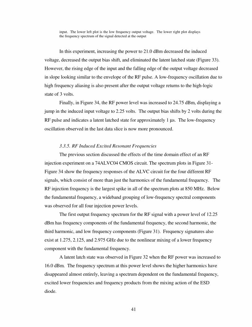
41
input. The lower left plot is the low frequency output voltage. The lower right plot displays
the frequency spectrum of the signal detected at the output
In this experiment, increasing the power to 21.0 dBm decreased the induced
voltage, decreased the output bias shift, and eliminated the latent latched state (Figure 33).
However, the rising edge of the input and the falling edge of the output voltage decreased
in slope looking similar to the envelope of the RF pulse. A low-frequency oscillation due to
high frequency aliasing is also present after the output voltage returns to the high-logic
state of 3 volts.
Finally, in Figure 34, the RF power level was increased to 24.75 dBm, displaying a
jump in the induced input voltage to 2.25 volts. The output bias shifts by 2 volts during the
RF pulse and indicates a latent latched state for approximately 1 µs. The low-frequency
oscillation observed in the last data slice is now more pronounced.
3.3.5. RF Induced Excited Resonant Frequencies
The previous section discussed the effects of the time domain effect of an RF
injection experiment on a 74ALVC04 CMOS circuit. The spectrum plots in Figure 31-
Figure 34 show the frequency responses of the ALVC circuit for the four different RF
signals, which consist of more than just the harmonics of the fundamental frequency. The
RF injection frequency is the largest spike in all of the spectrum plots at 850 MHz. Below
the fundamental frequency, a wideband grouping of low-frequency spectral components
was observed for all four injection power levels.
The first output frequency spectrum for the RF signal with a power level of 12.25
dBm has frequency components of the fundamental frequency, the second harmonic, the
third harmonic, and low frequency components (Figure 31). Frequency signatures also
exist at 1.275, 2.125, and 2.975 GHz due to the nonlinear mixing of a lower frequency
component with the fundamental frequency.
A latent latch state was observed in Figure 32 when the RF power was increased to
16.0 dBm. The frequency spectrum at this power level shows the higher harmonics have
disappeared almost entirely, leaving a spectrum dependent on the fundamental frequency,
excited lower frequencies and frequency products from the mixing action of the ESD
diode.
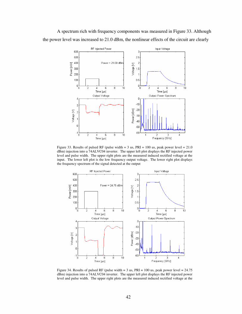
42
A spectrum rich with frequency components was measured in Figure 33. Although
the power level was increased to 21.0 dBm, the nonlinear effects of the circuit are clearly
Figure 33. Results of pulsed RF (pulse width = 3 us, PRI = 100 us, peak power level = 21.0
dBm) injection into a 74ALVC04 inverter. The upper left plot displays the RF injected power
level and pulse width. The upper right plots are the measured induced rectified voltage at the
input. The lower left plot is the low frequency output voltage. The lower right plot displays
the frequency spectrum of the signal detected at the output
Figure 34. Results of pulsed RF (pulse width = 3 us, PRI = 100 us, peak power level = 24.75
dBm) injection into a 74ALVC04 inverter. The upper left plot displays the RF injected power
level and pulse width. The upper right plots are the measured induced rectified voltage at the

43
input. The lower left plot is the low frequency output voltage. The lower right plot displays
the frequency spectrum of the signal detected at the output.
shown in this frequency spectrum with a large spike in a lower frequency range creating
spectral products almost up to 4 GHz.
Finally, in Figure 34 when the time domain showed latent latching for a 1 µs
interval, the fundamental frequency and its harmonics measured up to the fifth harmonic
dominated the frequency domain with additional components below 850 MHz and up to
the second harmonic.
The relevance of these excited oscillations with respect to the effects of RF is
twofold: one reason is that modulation of the RF signal can have a profound effect in
providing low frequency components to produce frequency products from the mixing
behavior of the p-n junction, and second, the RF is stimulating certain portions of the
circuit to cause additional frequency signals unrelated to the RF frequency to oscillate.
Since the impedances of the previous circuits showed voltage dependent resonances at
various frequencies, the addition of RF and excited oscillations feeding through to the
output of the circuit in combination with the propagating induced state change can cause
additional problems in the following circuits. The propagating frequency components can
potentially excite other resonances causing induced DC voltages and additional
oscillations.

44
CHAPTER 4 RF EFFECTS MODELING
4.1. Introduction
One objective of this thesis was to demonstrate that the RF effects on digital
electronics could be modeled to simulate the effects measured in experiments. PSPICE
was used to determine if the effects could be explained using simple models of the inverters
and lumped element circuits for parasitic elements. The diode parameters measured and
the block diagrams of the ESD protection topologies found in the data sheets of the
inverters were the basis for building the devices used in simulation models.
Although simulations have been performed on almost all the devices tested in this
research, only one or two examples will be used in showing an understanding for each of
the RF effects observed. Additional information and examples of simulations are included
in appendices where noted.
4.2. Models derived from measurements
Diode models were designed using the parameters extracted using the methods
outlined in Section 3.2. A list of the values used for the diode models is given in Table 4
for the different diode models created. The PSPICE circuit models for the CMOS inverter
circuits were based on the block diagrams of the ESD topologies given in the data sheets
and application notes for specific logic families and on direct measurements to determine
the accuracy of the block diagrams [21]-[24]. In certain cases, such as the ALVC CMOS
inverter, the block diagram implied an ESD protection element from ground to signal and
another element from signal to Vdd, in which case, the PSPICE models were modified
accordingly.
Since information regarding the MOSFETS in the inverters tested was not
available, Level 4 MOSFET models based on the 2.0 micron Orbit process at MOSIS were
used in all the simulations [27].

45
Table 4. Diode parameters used for each of the ESD diodes for the various
circuits simulated.
Diode Models
Parameter Units ESD_ACT ESD_LVX ESD_LVX_Vdd ESD_HCT
IS A 4.00E-15 5.00E-12 5.00E-12 1.00E-12
N 1.121 1.05 1.5 1.05
RS Ω 13 8 20 8
IKF A 0 0 0 0
XTI 3 3 3 3
EG eV 1.11 1.11 1.11 1.11
CJO F 3.00E-12 3.80E-12 3.80E-12 3.60E-12
M 0.3 0.3 0.3 0.3
VJ V 0.5 0.7 0.7 0.7
FC 0.5 0.5 0.5 0.5
ISR A 4.00E-15 1.00E-10 1.00E-10 1.00E-10
NR 2 2 2 2
BV V 3.5 20 10 20
IBV A 0.0001 0.0001 0.001 0.0001
TT s 1.00E-09 1.00E-09 1.00E-09 1.00E-09
4.3. Simulated Port Characteristics
The port characteristics of interest are the input impedance and drive curves (RF to
DC conversion curves). The process started with simple circuit explanations for input
impedance resonance; then, more complex models based on extracted diode parameters and
taking into account parasitic elements were designed to simulate measured input impedance
curves. A circuit was then designed and modified to match a measured RF amplitude to DC
conversion drive curve.
4.3.1. Input Impedance and Resonance
The resonance dips observed in the input impedances measured in the CMOS
inverters in Section 3.2 can be explained by the resonance formed by an inductor and
capacitor in series. A simple series resonant tank circuit was designed in PSPICE to
determine the effects of varying the capacitance to simulate the voltage dependent
capacitance of a p-n junction. The circuit simulated is shown in Figure 35(a) using a high
valued coupling resistor, bias resistor and load resistor. A value of 4 nH was assigned to
the input inductor meant to simulate the inductance due to an package pin and bonding
wire. The capacitor Cj was varied over the values 6-10 pF in 1 pF steps. An AC analysis

46
revealed that as the capacitance decreased from 10 pF to 6 pF, the resonances shifted from
800 MHz to just above 1 GHz (Figure 35b). A decrease in capacitance of 40% was shown
for a voltage shift from 0 to 3 volts in the voltage dependent capacitance curves of Figure 6,
which is reproduced for convenience in Figure 36(a). Measurements and datasheets from
manufacturers have shown that inductances in the devices tested had values between 6-8
nH and zero-bias capacitances due to the p-n junctions in ESD protection circuits valued
between 3-4 pF. The resonant frequencies formed by these reactive elements are in the
region of 500 MHz-1.5 GHz. When compared to the input impedance measurements
shown in Figure 15, the location and shift in resonant frequencies are very similar.
(a)
(b)
Figure 35. A simulation showing resonances caused by using (a) a simple
circuit with an inductor and capacitor in series creating and (b) the resulting
impedance. The capacitor Cj was varied over the values 6 pF (green), 7 pF
(red), 8 pF (purple), 9 pF (yellow), and 10 pF (magenta) to create a change in
the resonance frequency of 200 MHz (compare with the measured results in
Figure 15).

47
(a) (b)
Figure 36. (a) A comparison plot of the voltage dependent capacitances
showing variation as a function of bias voltages for an ESD diode from ground
to the signal line (Lower Diode) and an ESD diode from the signal line to Vdd
(Upper Diode). The diodes were assumed to be matched with ϕbi = 0.7 volts
and n = 0.5. (b) A plot of the change in the resonant frequency of upper and
lower diodes with Cj0 = 3.5 pF and L = 7 nH.
Using a diode with a zero biased capacitance of 3.5 pF in series with an inductor of
7 nH in the equation for the resonant frequency:
1
2 * ( )f
L C Vπ= (16)
the voltage dependent resonant frequencies are graphed in Figure 36b, where plots for the
resonant frequencies due to upper and lower ESD diodes are compared.
A more advanced model was designed to take into account additional parasitic
elements to model the frequency response observed in a 74ALVC04 CMOS inverter
(Figure 37b). The elements of the injection point were changed into a 100 pF DC blocking
capacitor and a 100 µH RF choke. An additional inductor was added between the anode of
the diode and ground to take into account the corresponding bonding wire in the actual
circuit. To model the effect of the gate capacitances of the MOSFETs, a capacitance of 0.7
pF was added in parallel to the ESD diode. A parasitic capacitor and resistor were added in
parallel to the inductors to account for additional package parasitics, which created the
resonance at 1.8 GHz. The values for the circuit elements in the simulation were modified
in attempts to match the resonances and their quality factors. Differences in the plots are
attributed to unaccounted parasitic elements in the simulation model.

48
(a) (b)
Figure 37. (a) A plot showing the comparison of the input impedance of a
74ALVC04 circuit measurements to the results of the simulation circuit in (b).
The measured data for the input bias voltage of 0.0 and 2.0 volts are red and
blue, respectively, and the calculate impedance form the simulation are purple
and green for bias voltages of 0.0 and 2.0 volts, respectively.
The frequency response of the input ports of the inverters provided insight into
susceptibilities as well as excited frequencies from the inverters. As devices are becoming
smaller in transistor size and in packaging sizes, the parasitic inductances and capacitances
become more of a concern as their resonant frequencies are within the microwave
frequency range. The parasitic inductances are due to the bonding wires, which lead from
the pins of the packaging from the outside world to the bonding pads located on the
substrate of the chip. Parasitic capacitances are related to the bonding pads, power line
buses, and from the ESD protection devices located at the input and output ports of the
device.
4.3.2. Drive Curves
Drive curves were measured and simulated to determine the validity of the ESD
diode models. A drive curve is normally associated with amplifiers to determine the
transfer response of the input signal to the gain of the output signal with respect to a
particular frequency. In this case, the drive curve is defined as the transfer function due to
rectification of the input RF amplitude in voltage to the induced DC voltage. The
experiment performed was set up as in Figure 11 with the circuit in normal operating mode
and a power supply voltage of 3 volts. A probe was placed at the input of the inverter to

49
measure the induced DC voltage across the pull-up resistor. The RF pulse width was set to
2.0 µs with a PRI of 10.0 ms, and the frequency was always the resonant frequency on the
device. The measured voltage was the average of the rectified RF envelope.
A PSPICE circuit model of the LVX was made based on the block diagram found
in the LVX datasheet where lower and upper ESD protection diodes were shown to exist in
Figure 38. A drive curve simulation was performed by using a CW RF signal at the
resonant frequency of the circuit, delaying the simulation to a time where the rectified
voltage had stabilized, sweeping the RF amplitude, and measuring the induced DC voltage.
The induced voltage was measured through a low-pass filter with an upper cutoff frequency
of 100 MHz.
(a)
(b)
Figure 38. (a) RF to DC drive curve and (b) PSPICE circuit used to match
simulation results with measurements for the LVX inverter.
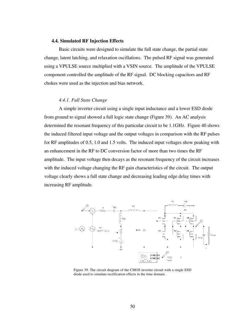
50
4.4. Simulated RF Injection Effects
Basic circuits were designed to simulate the full state change, the partial state
change, latent latching, and relaxation oscillations. The pulsed RF signal was generated
using a VPULSE source multiplied with a VSIN source. The amplitude of the VPULSE
component controlled the amplitude of the RF signal. DC blocking capacitors and RF
chokes were used as the injection and bias network.
4.4.1. Full State Change
A simple inverter circuit using a single input inductance and a lower ESD diode
from ground to signal showed a full logic state change (Figure 39). An AC analysis
determined the resonant frequency of this particular circuit to be 1.1GHz. Figure 40 shows
the induced filtered input voltage and the output voltages in comparison with the RF pulses
for RF amplitudes of 0.5, 1.0 and 1.5 volts. The induced input voltages show peaking with
an enhancement in the RF to DC conversion factor of more than two times the RF
amplitude. The input voltage then decays as the resonant frequency of the circuit increases
with the induced voltage changing the RF gain characteristics of the circuit. The output
voltage clearly shows a full state change and decreasing leading edge delay times with
increasing RF amplitude.
Figure 39. The circuit diagram of the CMOS inverter circuit with a single ESD
diode used to simulate rectification effects in the time domain .
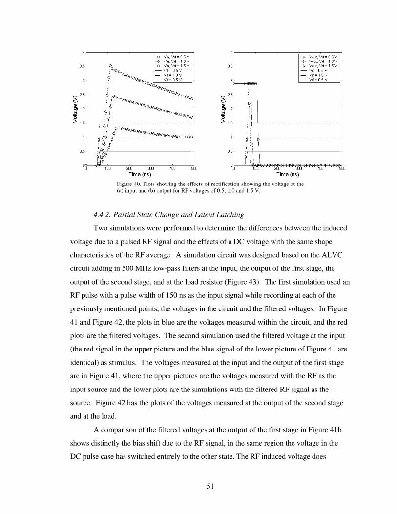
51
Figure 40. Plots showing the effects of rectification showing the voltage at the
(a) input and (b) output for RF voltages of 0.5, 1.0 and 1.5 V.
4.4.2. Partial State Change and Latent Latching
Two simulations were performed to determine the differences between the induced
voltage due to a pulsed RF signal and the effects of a DC voltage with the same shape
characteristics of the RF average. A simulation circuit was designed based on the ALVC
circuit adding in 500 MHz low-pass filters at the input, the output of the first stage, the
output of the second stage, and at the load resistor (Figure 43). The first simulation used an
RF pulse with a pulse width of 150 ns as the input signal while recording at each of the
previously mentioned points, the voltages in the circuit and the filtered voltages. In Figure
41 and Figure 42, the plots in blue are the voltages measured within the circuit, and the red
plots are the filtered voltages. The second simulation used the filtered voltage at the input
(the red signal in the upper picture and the blue signal of the lower picture of Figure 41 are
identical) as stimulus. The voltages measured at the input and the output of the first stage
are in Figure 41, where the upper pictures are the voltages measured with the RF as the
input source and the lower plots are the simulations with the filtered RF signal as the
source. Figure 42 has the plots of the voltages measured at the output of the second stage
and at the load.
A comparison of the filtered voltages at the output of the first stage in Figure 41b
shows distinctly the bias shift due to the RF signal, in the same region the voltage in the
DC pulse case has switched entirely to the other state. The RF induced voltage does
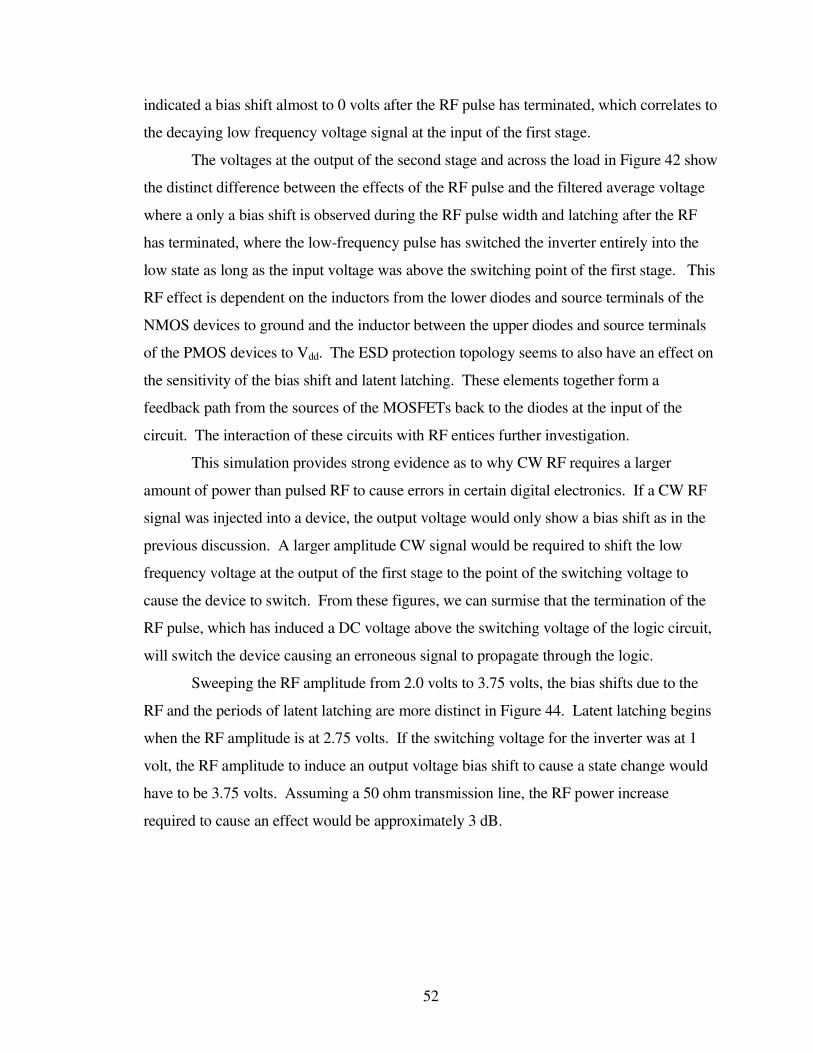
52
indicated a bias shift almost to 0 volts after the RF pulse has terminated, which correlates to
the decaying low frequency voltage signal at the input of the first stage.
The voltages at the output of the second stage and across the load in Figure 42 show
the distinct difference between the effects of the RF pulse and the filtered average voltage
where a only a bias shift is observed during the RF pulse width and latching after the RF
has terminated, where the low-frequency pulse has switched the inverter entirely into the
low state as long as the input voltage was above the switching point of the first stage. This
RF effect is dependent on the inductors from the lower diodes and source terminals of the
NMOS devices to ground and the inductor between the upper diodes and source terminals
of the PMOS devices to Vdd. The ESD protection topology seems to also have an effect on
the sensitivity of the bias shift and latent latching. These elements together form a
feedback path from the sources of the MOSFETs back to the diodes at the input of the
circuit. The interaction of these circuits with RF entices further investigation.
This simulation provides strong evidence as to why CW RF requires a larger
amount of power than pulsed RF to cause errors in certain digital electronics. If a CW RF
signal was injected into a device, the output voltage would only show a bias shift as in the
previous discussion. A larger amplitude CW signal would be required to shift the low
frequency voltage at the output of the first stage to the point of the switching voltage to
cause the device to switch. From these figures, we can surmise that the termination of the
RF pulse, which has induced a DC voltage above the switching voltage of the logic circuit,
will switch the device causing an erroneous signal to propagate through the logic.
Sweeping the RF amplitude from 2.0 volts to 3.75 volts, the bias shifts due to the
RF and the periods of latent latching are more distinct in Figure 44. Latent latching begins
when the RF amplitude is at 2.75 volts. If the switching voltage for the inverter was at 1
volt, the RF amplitude to induce an output voltage bias shift to cause a state change would
have to be 3.75 volts. Assuming a 50 ohm transmission line, the RF power increase
required to cause an effect would be approximately 3 dB.
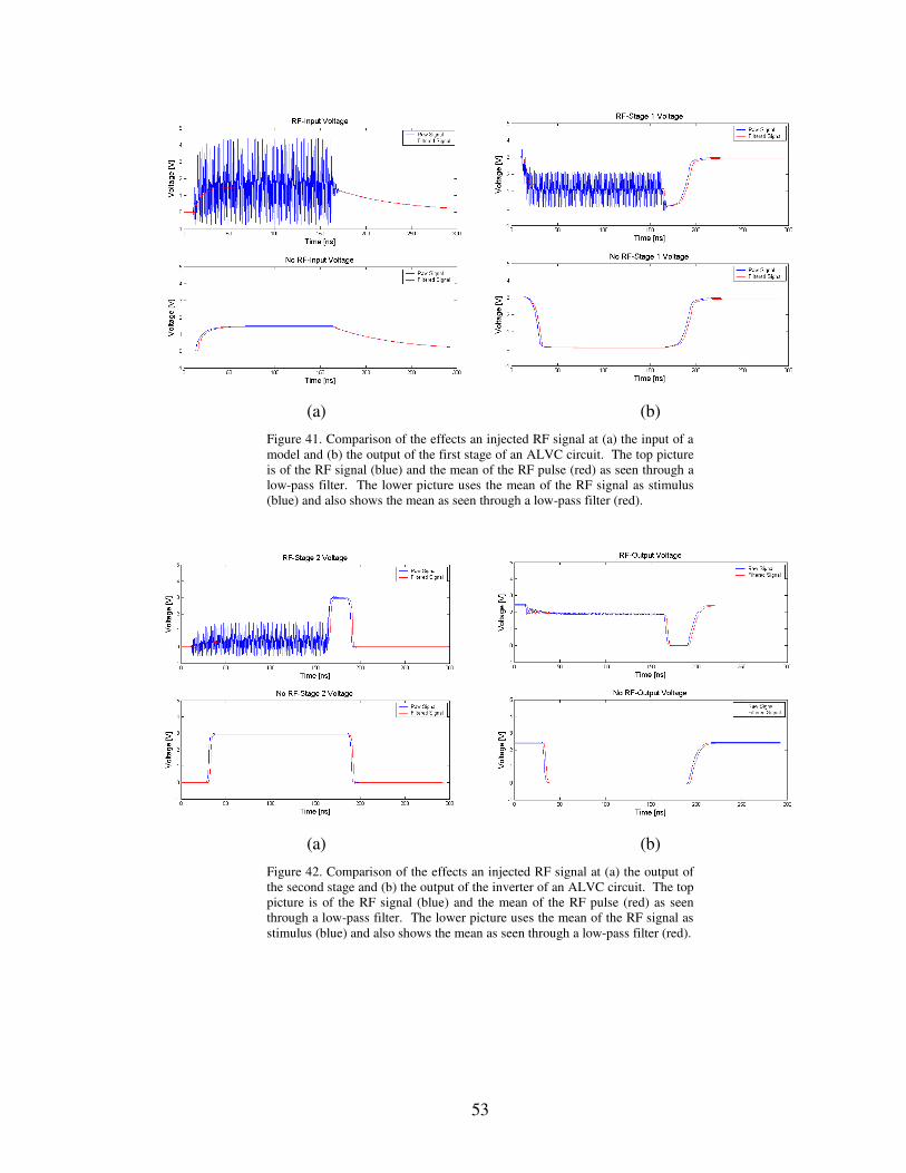
53
(a) (b)
Figure 41. Comparison of the effects an injected RF signal at (a) the input of a
model and (b) the output of the first stage of an ALVC circuit. The top picture
is of the RF signal (blue) and the mean of the RF pulse (red) as seen through a
low-pass filter. The lower picture uses the mean of the RF signal as stimulus
(blue) and also shows the mean as seen through a low-pass filter (red).
(a) (b)
Figure 42. Comparison of the effects an injected RF signal at (a) the output of
the second stage and (b) the output of the inverter of an ALVC circuit. The top
picture is of the RF signal (blue) and the mean of the RF pulse (red) as seen
through a low-pass filter. The lower picture uses the mean of the RF signal as
stimulus (blue) and also shows the mean as seen through a low-pass filter (red).

54
Figure 43. Circuit diagram for the waveforms with RF stimulus in Figure 41
and Figure 42. The circuit diagram for the DC waveforms is similar but
replaced the RF source with a file input source.
Figure 44. Output voltages of the SPICE circuit model in Figure 43, which
show for most RF voltages the device going into hard conduction after the RF
pulse. The RF pulse is varied in amplitude from 2.0 to 3.75 volts in 0.25 volt
increments. The RF had a center frequency of 1.0 GHz, and a pulse width of
150 ns and was delayed by 10 ns.

55
4.4.3. RF Gain
A CMOS inverter with an input bias voltage close to the switching level will
conduct like a Class-A amplifier. While one of the MOS transistors is conducting, the
output of the other transistor will act as an active load. Over a range of voltages around the
switching voltage, the inverter acts as a linear amplifier with high gain [28]. The general
equation for the gain of MOSFET amplifier is given as
*( )v m o dA g r R= − (17)
where gm is the transconductance of the MOSFET, ro is the output resistance of the
MOSFET, and Rd is the load impedance as seen at the drain. In this case, the drain
resistance is the active load of the other MOSFET and the input impedance of the next
inverter stage. Since the inverters are buffered, we expect the DC gain of the second and
third inverters to be very high, essentially limiting the bias voltages to these stages to
ground and Vdd. The MOSFETs would be expected to be operating in their triode regions
limiting the Class-A conduction effect of the devices.
To determine the RF gain in between the CMOS stages excluding the effect of the
RF enhancement from input impedance resonances, a small-signal AC analysis was
performed on the circuit in Figure 43 measuring the RF voltage gain between the input and
output of each inverter stage, and between the input and output of all three stages. Figure
45 shows the RF gains when the circuit is biased in the low (0.5 volts) and high (2.5 volts)
logic states and the AC signal was 10 mV.
An amazing gain of almost 20 dB is calculated for Stage 2 at 700 MHz in the low
bias case. However, with the accumulation of effect from all threes stages, the peak of –15
dB near 900 MHz is calculated in the low bias case.
The small-signal transfer functions for all the three circuits showed drastic changes
as the input voltage was swept from 0 to 3 volts, with a huge jump when the input voltage
reached the switching voltage. In the high-bias case, the transfer functions of all three
stages have changed dramatically from the low-bias case. The AC transfer curve of the
entire circuit showed a gain of almost 0 dB at 1GHz. This simulation shows the potential
of no RF loss between the CMOS inverters at certain frequencies.

56
(a) (b)
Figure 45. The AC gain between the first stage, second stage, third stage, and
the entire CMOS inverter for (a) low logic state (vbias = 0.5 volts) and (b) high
logic state (vbias = 2.5 volts).
4.4.4. Relaxation Oscillations
In Section 3.3.4, the ALVC CMOS inverter showed low frequency oscillations
referenced as relaxation oscillations. The frequency of the RF signal in that experiment
was slightly above the zero-bias resonant frequency of the input impedance. Figure 46 is a
basic circuit diagram of the LVC circuit containing a single ESD diode from ground to the
signal line and inductors at the input, to the power supply voltage and to ground. The
PSPICE input impedance resonance was calculated to be 688 MHz. An RF injection
frequency of 850 MHz was arbitrarily chosen for this simulation. For an RF amplitude of
1.5 volts, the filtered input and output voltages of Figure 47 shows the distinct sawtooth
waveform of the relaxation oscillations. With increasing RF amplitude in this simulation,
the magnitude of the relaxation oscillations increased and the frequency of the sawtooth
waveform varied. Several simulations have shown that the inductance from the anode of
the ESD diode and source of the NMOS circuits to ground seems to be a critical component
in causing this effect.

57
Figure 46. PSPICE circuit of LVC CMOS inverter, which simulated relaxation
oscillations as seen in Figure 47.
Figure 47. PSPICE simulation output of a LVC type of circuit showing the
induced RF at the input with relaxation oscillations and a bias shift at the output
including relaxation oscillations and latent latching.

58
CHAPTER 5 CONCLUSION AND FUTURE WORK
5.1. Conclusion
This thesis focused on the effects of RF pulses on digital electronics. The following
is a summary on each of the major points in the chapters.
The theory of the common circuit elements found in CMOS inverters was described
in Chapter 2. The input circuit of CMOS inverters includes the ESD protection circuits,
which consist of at least one diode or p-n junction. A series expansion of the ideal diode
model showed that the second-order term produces an induced DC voltage. The amplitude
of the induced voltage is dependent on the saturation current of the diode, the video
resistance in the diode, the RF amplitude, and the load impedance as seen by the diode.
Bandwidth considerations for signal detection and measurements were discussed from a
frequency point of view and how it should be applied to measurements.
The equations describing the operation of CMOS inverters indicate the switching
voltages of the devices are dependent on the power supply voltage and characteristics of the
MOSFETS. Logic circuits are also known to have problems with logic-pulse characteristics
with edges, which are very slow or very fast. The frequency components of the logic pulse
can cause oscillations to occur leading to operation instability. Circuitry added to CMOS
devices such as Schmitt Trigger devices and Bus-Hold Circuitry use additional Inverter
stages to feed back DC voltages, potentially leading to feedback loops for RF signal.
Chapter 3 provided details of the results of experimental measurements performed
in this research. The circuit setups described were used for a majority of the injection
experiments. Bandwidth considerations were taken into account when attempting to
measure the induced voltages and finding a method of efficiently coupling RF into the
circuits. Loading problems were also discussed as playing a large factor in choosing DC
blocking capacitors and RF chokes. The injection experiments required blocking
capacitors which acted as 50 ohm transmission lines at the injection frequency required
while acting as a high impedance line at lower frequencies. The RF choke had to be such
that the DC pulse with large frequency components (up to 100 MHZ) can be measured
while blocking frequencies above 200 MHz. A suggested method for enhancing the
transfer function of the reactive elements was by using high-pass filters in place of DC
blocking capacitors and low-pass filters for RF chokes.

59
The DC and high frequency input port characteristics were measured for several
families of CMOS inverters including the AHC, AHCT, HC, HCT, LVC, ALVC, LVC,
and LVX. The IV relations for several CMOS inverters were used to determine the
existence of a diode type device located at the input of the circuits of interest. The DC
diode characteristics were extracted using a sensitive multimeter and used to determine the
saturation current and ideality coefficient. Voltage dependent input impedance resonances
were found in all of these devices, which varied up to 200 MHz with a change in voltage
corresponding to a low logic state to a high logic state. A method to measure and calculate
the high frequency capacitance of the variable p-n junction capacitance was discussed and
used to incorporate the values into SPICE models.
The results from threshold power injection experiments on several families of logic
circuits showed that low powered RF pulses (down to 0 dBm) could cause state changes.
The CMOS logic families tested included AC, ACT, AHC, AHCT, HC, HCT, ALVC,
LVC, LCX, LVX, and VHC. A 1/f2 relation in the 1-6 GHz range was observed in the
required power for most of these circuits. Operating power supply voltages showed a
direct correlation to the switching voltage and required threshold hold power levels.
Changes in power supply voltages showed a change of 15 dB to cause effects. Input bias
levels also played a role in the threshold power levels for CMOS inverters affecting the
susceptibility of a circuit. A change in input logic state change showed a difference up to
20 dB in RF power to cause effects between low and high logic levels. In some cases, state
changes were never observed.
Changes in the power supply current corresponding to the state changes output
voltage bias shifts in CMOS inverters were measured. These shifts indicated regions of
input bias levels where the MOSFETs of the inverters enter into Class A conduction
operation leading to larger RF gains. The increased RF gains of the MOSFETS also
correspond to large variations in the Miller capacitances of the devices potentially affecting
the rectification sensitivity of the ESD diodes and the observed input impedance resonance
frequency.
RF feedthrough and gain were measured at the outputs of the HCT and LCX
devices. The amplitude of the RF measured in the output waveforms depended on RF
60
amplitude and input bias voltage. RF gains up to 2 dB were measured in the HCT device
and 3 dB in the LCX inverter.
Different circuits showed different respondes to pulsed RF signals. Depending on
the circuit and the input bias, devices showed logical state changes during the RF pulse,
output voltage bias shifts during the pulse, logical state changes after the termination of the
RF pulse, or no response at all. With circuits showing state changes during and after the
RF pulse, output voltages were shown to potentially switch the inverters longer than the
pulse width of the injected RF signal. This latent latching was also observed in devices that
only showed output voltage bias shifts during the RF pulse. Latent latching corresponded
to the induced voltage level and RC time constant at the input of the device, keeping the
device switched until the input voltage dropped below the switching point of the device.
Frequency domain measurements during injection experiments indicated excited
circuit resonances occurred. The fundamental frequency, several of its harmonics, low-
frequency signals and the IM products of all these signals were recorded at different power
levels during the experiment. Induced oscillations were also observed in the time domain,
which were seen as sawtooth waveforms at the input and output of the devices measured.
Chapter 4 discussed the results of simple simulation circuits designed in PSPICE
modeling the effects observed for the CMOS inverters. Block diagrams of the ESD
protection circuit topology in data sheets of the various devices were used as the basis for
input circuits of the simulation models. Diode models were created based on extracted DC
and high frequency characteristics. The resonances measured in the input impedances of
CMOS inverters were reproduced using models of inductors in series with variable
capacitors. The inductances were attributed to the bonding wires measured in the 4-8 nH
range. The p-n junctions of the ESD protection circuits were the sources of voltage
dependent capacitances, which caused the resonant frequencies to shift up by 200 MHz as
the input bias shift from a low logic level to a high logic level. A simulation model of the
input impedance of the ALVC CMOS inverter taking into account various parasitic
elements gave very good agreement to measured data for resonance shifts from a low bias
input to a high bias input.
To determine the accuracy of the RF signal to DC conversion, rectification drive
curves were simulated. The parasitic elements of the circuits for the LVX and ACT CMOS

61
inverters were modified until good agreement was made between the simulation and
measured data.
State changes due to induced rectification at the input were observed in simulation
circuits where the bonding wire inductance for the ground and Vdd pin did affect RF
rectification. Circuits without an inductor at this junction showed RF gain due to resonance,
RF signal rectification and a state change in the logic circuit corresponding to the injected
RF pulse. However, when the ground and Vdd inductance was a factor and used as
components in simulation circuits, output voltage bias shifts, latent latching and relaxation
oscillations were all found to be modeled by creating output voltage waveforms predicting
behaviors observed in the measured RF injection experiments. The bias shifts in the output
voltage during RF pulsed signals that also show latent latching after the RF pulse
terminated gave evidence as to why threshold power levels for RF pulse modulated signals
to cause effects in circuits can be from 3-10 dB less than the threshold power levels for CW
RF signals.
The AC gain was also calculated using a CMOS circuit which demonstrated the
input bias has an effect on the RF transfer curves of each stage of the inverter as well as the
entire circuit. Depending on the input logic state and the frequency, the RF was shown to
potentially pass through a circuit with little or no attenuation.
Theoretical analysis, measurements and simulations have shown that the most
sensitive rectification elements in logic circuits are the ESD protection elements. With RF
amplitude enhancement from input impedance resonances, induced voltages from ESD
diodes, RF feed through, exciting parasitic circuit resonances, low-powered pulsed RF
signals have been shown to be able to affect the correct operation of digital electronics.

62
5.2. Considerations for Future Work
This section contains some ideas for follow-up areas of research based on the
findings in this paper. Because of the breadth of this subject with so many different
avenues of research that can be explored, the following are just some major tasks that could
be considered.
A Cascade RF probe station has been setup for the characterization of ESD
protection ggNMOS and two-stage inverter designed through MOSIS (Figure 48). The on-
chip probing will eliminate the effects of the package parasitic elements. RF injection will
also be performed to determine the rectification efficiency of the ESD ggNMOS.
Additional commonly used ESD topologies could be designed through MOSIS and
modeled to evaluate the susceptibility of these devices. A comparison between inverters
with and without ESD protection circuits could also be done to determine the rectification
sensitivity between the different circuits.
As a follow-up to the experiments performed by Kenneally in [86], the packages of
COTS CMOS inverters could be removed to expose the internal circuitry. By using the
Focused Ion Beam (FIB) at the University of Maryland, injection and port characteristic
testing could be performed at different stages while severing different portions of the ESD
protection devices from the main inverter circuit.
Figure 48. MOSIS chip designed to test S-parameters of ESD structures and to
use in RF injection experiments.

63
Since the lumped element circuits showed very similar characteristics as the
measurements, building models and performing simulations in HSPICE or other high
frequency circuit simulation package would be the next step in modeling these effects. A
more complete analysis can be performed in calculating high frequency effects such as
power reflections and potential points of radiation.
RF injection experiments using chaotic or wideband modulated waveform should
also be considered. Initial testing showed very promising results in causing state changes
and exciting a wide range of resonances. These types of signals could excite a wide variety
of input resonances affecting more than one type of circuit. With the aspects of RF gain
and feedthrough, a signal covering a very large frequency range will have more of a chance
of causing an effect.
Based on all the findings here, one very large area of research could be to determine
the probabilities to cause errors in large systems of circuits. Using the basis of different
pulse characteristics of interfering signals, the timing issues of latent latching, logic states
of the devices under test, and the potential of inducing oscillations the rate of failure or
errors could be calculated to determine susceptibility and rate of errors regarding all types
of electromagnetic interference.
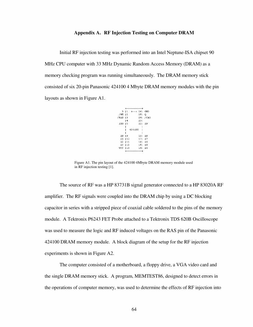
64
Appendix A. RF Injection Testing on Computer DRAM
Initial RF injection testing was performed into an Intel Neptune-ISA chipset 90
MHz CPU computer with 33 MHz Dynamic Random Access Memory (DRAM) as a
memory checking program was running simultaneously. The DRAM memory stick
consisted of six 20-pin Panasonic 424100 4 Mbyte DRAM memory modules with the pin
layouts as shown in Figure A1.
Figure A1. The pin layout of the 424100 4Mbyte DRAM memory module used
in RF injection testing [1].
The source of RF was a HP 83731B signal generator connected to a HP 83020A RF
amplifier. The RF signals were coupled into the DRAM chip by using a DC blocking
capacitor in series with a stripped piece of coaxial cable soldered to the pins of the memory
module. A Tektronix P6243 FET Probe attached to a Tektronix TDS 620B Oscilloscope
was used to measure the logic and RF induced voltages on the RAS pin of the Panasonic
424100 DRAM memory module. A block diagram of the setup for the RF injection
experiments is shown in Figure A2.
The computer consisted of a motherboard, a floppy drive, a VGA video card and
the single DRAM memory stick. A program, MEMTEST86, designed to detect errors in
the operations of computer memory, was used to determine the effects of RF injection into

65
Figure A2. The block diagram of the layout for the RF injection experiment
into a Panasonic 424100 DRAM memory module.
the DRAM module [28]. The program works by temporarily writing a series of ”0’s” and
“1’s” to different locations in the memory module, and then reads back the data words to
determine if any of the memory blocks had been corrupted. Any errors encountered were
reported to the monitor displaying the test, which was currently running, and the location in
the memory where the error occurred.
The memory module has several different pins associated with the functionality of
the device, particularly the write enable pin (/WE), the input data pin (D), the output data
pin (Q), the row-address strobe (/RAS), the column-address strobe (/CAS), the address pins
(A0-A10), the ground pin (GND), and the power supply pin (VCC). All of these pins were
tested for susceptibility to RF, which demonstrated the RAS pin was more susceptible than
the other pins by almost 15 dBm. The power supply pin and clock pins were the most
robust of all the pins tested and showed no effect of RF power levels up to 25 dBm.
Injections into the RAS pin were used for the experiments described below.
Continuous wave (CW) RF signals were injected into DRAM memory module over
a range of frequencies and increasing the power level until an error was detected. Power

66
threshold tests were performed using the on-screen error reporting of MEMTEST 86 as an
indicator to bit upset. The RF power levels were increased incrementally until a series of
errors appeared on the monitor, the monitor began displayed unusual characters hiding the
diagnostics reported by MEMTEST 86, or the system would not respond to external
stimulus and required a reboot of the computer to function normally.
Voltage measurements taken at the RAS pin during RF injection demonstrated
voltage bias shifts of the digital logic voltages levels. An experiment with CW RF with a
frequency of duty factor of 50% and pulse width of 150 ns injected into the RAS pin
demonstrated a +1 volt bias shift from the low state and a -1 volt bias shift from the high
state as seen during a data pulse (Figure A3). The measurement also showed a sinusoidal
signal coupled onto the induced voltage, which had a frequency corresponding to the 33
MHz clock frequency of the memory module.
For a comparison to the effect of pulse modulating, the RF signal was modulated
with a duty factor of 50%, a pulse width of 150 ns, keeping the frequency at 1.965 GHz,
Figure A3. The input voltage measured at the RAS pin (blue) before and (red)
after an injected CW signal with a frequency of 1.965 GHz and a power level
of 26.0 dBm showing an induced bias shift due to the RF signal. The induced
voltage shifted the logic levels by one volt in the low and high logic states and
also had the 33 MHz clock signal of the memory module couple onto the
voltage line.
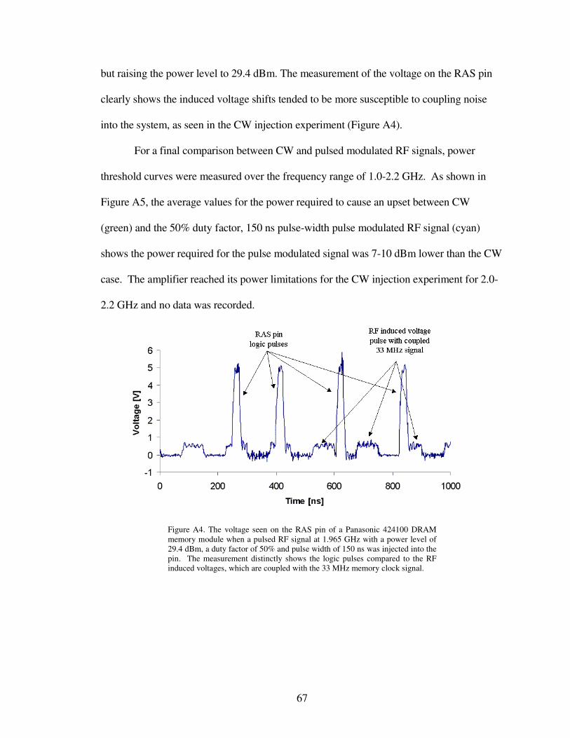
67
but raising the power level to 29.4 dBm. The measurement of the voltage on the RAS pin
clearly shows the induced voltage shifts tended to be more susceptible to coupling noise
into the system, as seen in the CW injection experiment (Figure A4).
For a final comparison between CW and pulsed modulated RF signals, power
threshold curves were measured over the frequency range of 1.0-2.2 GHz. As shown in
Figure A5, the average values for the power required to cause an upset between CW
(green) and the 50% duty factor, 150 ns pulse-width pulse modulated RF signal (cyan)
shows the power required for the pulse modulated signal was 7-10 dBm lower than the CW
case. The amplifier reached its power limitations for the CW injection experiment for 2.0-
2.2 GHz and no data was recorded.
Figure A4. The voltage seen on the RAS pin of a Panasonic 424100 DRAM
memory module when a pulsed RF signal at 1.965 GHz with a power level of
29.4 dBm, a duty factor of 50% and pulse width of 150 ns was injected into the
pin. The measurement distinctly shows the logic pulses compared to the RF
induced voltages, which are coupled with the 33 MHz memory clock signal.

68
Figure A5. A plot comparing the threshold power levels of (red) CW and (dark
blue) pulsed RF signals, which caused errors in a Panasonic 424100 DRAM
memory module. The pulse modulation had a 50% duty factor with a pulse
width of 150 ns. Third order polynomial fits are also shown for CW (green) and
pulsed RF (cyan) signals to approximate the averages of the threshold power
levels. The amplifier reached the power limitations for the CW case for 2GHz
and above, thus no data was recorded.

69
Appendix B. I-V Characteristics of Inputs and Outputs for Various Digital
Families
The I-V characteristics of the 74HC04, 74HCT04, 74AHC04, and 74AHCT04 were
measured on a HP4145B Semiconductor Parameter Analyzer. Four measurements were
taken with the first port acting as the voltage reference: ground to input, input to Vdd,
ground to output, and output to Vdd. The HP4145B had the upper and lower current limits
set to +/- 50 µA, respectively.
Figure B 1. Input and output I-V characteristics for 74HC04.
Figure B 2.Input and output I-V characteristics for 74HCT04.

70
Figure B 3. Input and output I-V characteristics for 74AHC04.
Figure B 4. Input and output I-V characteristics for 74AHCT04.

71
Appendix C. Input impedance of various CMOS Inverters
(a)
(b)
Figure C 1. Frequency response of the (a) input impedance and (b) phase of the
74HCT04 CMOS Hex inverter.

72
(a)
(b)
Figure C 2. Frequency response of the (a) input impedance and (b) phase of the
74ALVC04 CMOS Hex inverter.

73
(a)
(b)
Figure C 3. Frequency response of the (a) input impedance and (b) phase of the
74LVC04 CMOS Hex inverter.

74
(a)
(b)
Figure C 4.Frequency response of the (a) input impedance and (b) phase of the
74LVX04 CMOS Hex inverter.
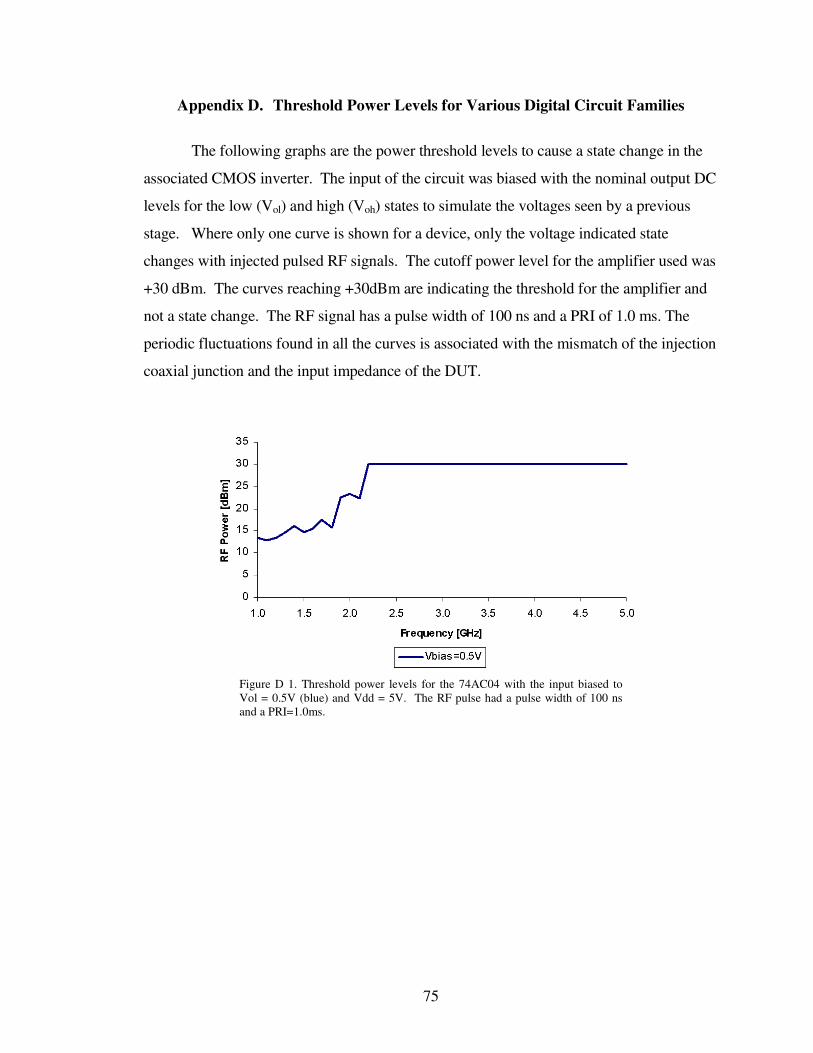
75
Appendix D. Threshold Power Levels for Various Digital Circuit Families
The following graphs are the power threshold levels to cause a state change in the
associated CMOS inverter. The input of the circuit was biased with the nominal output DC
levels for the low (Vol) and high (Voh) states to simulate the voltages seen by a previous
stage. Where only one curve is shown for a device, only the voltage indicated state
changes with injected pulsed RF signals. The cutoff power level for the amplifier used was
+30 dBm. The curves reaching +30dBm are indicating the threshold for the amplifier and
not a state change. The RF signal has a pulse width of 100 ns and a PRI of 1.0 ms. The
periodic fluctuations found in all the curves is associated with the mismatch of the injection
coaxial junction and the input impedance of the DUT.
Figure D 1. Threshold power levels for the 74AC04 with the input biased to
Vol = 0.5V (blue) and Vdd = 5V. The RF pulse had a pulse width of 100 ns
and a PRI=1.0ms.

76
Figure D2. Threshold power levels for the 74ACT04 with the input biased to
Vol = 0.4V (blue) and Vdd = 5V. The RF pulse had a pulse width of 100 ns
and a PRI=1.0ms.
Figure D3. Threshold power levels for the 74AHC04 with the input biased to
Voh = 0.5V (red) and Vdd = 5V. The RF pulse had a pulse width of 100 ns and
a PRI=1.0ms.

77
Figure D4. Threshold power levels for the 74AHCT04 with the input biased to
Vol = 0.4V (blue), Voh = 2.4V (red), and Vdd = 3.3V. The RF pulse had a
pulse width of 100 ns and a PRI=1.0ms.
Figure D5. Threshold power levels for the 74HC04 with the input biased to
Voh = 4.44V (red) and Vdd = 5V. The RF pulse had a pulse width of 100 ns
and a PRI=1.0ms.

78
Figure D6. Threshold power levels for the 74HCT04 with the input biased to
Vol = 0.4V (blue), Voh = 2.4V (red), and Vdd = 5V. The RF pulse had a pulse
width of 100 ns and a PRI=1.0ms.
Figure D7. Threshold power levels for the 74ALVC04 with the input biased to
Vol = 0.1V (blue), Voh = 3.2 V (red), and Vdd = 3.3V. The RF pulse had a
pulse width of 100 ns and a PRI=1.0ms.

79
Figure D8. Threshold power levels for the 74LVC04 with the input biased to
Vol = 0.4V (blue), Voh = 2.4V (red), and Vdd = 3.3V. The RF pulse had a
pulse width of 100 ns and a PRI=1.0ms.
Figure D9. Threshold power levels for the 74LCX04 with the input biased to
Voh = 2.4V (red) and Vdd = 3.3V. The RF pulse had a pulse width of 100 ns
and a PRI=1.0ms.

80
Figure D10. Threshold power levels for the 74LVX04 with the input biased to
Voh = 3.2V (red) and Vdd = 5V. The RF pulse had a pulse width of 100 ns and
a PRI=1.0ms.
Figure D11. Threshold power levels for the 74VHC04 with the input biased to
Vol = 0V (blue), Voh = 3.3V (red), and Vdd = 5V. The RF pulse had a pulse
width of 100 ns and a PRI=1.0ms.

81
Appendix E. Drive Curve for ACT Device
(a)
(b)
Figure E 1. (a) Drive curve for the ACT CMOS inverter and (b) the PSPICE
circuit diagram used for the drive curve simulation.

82
Appendix F. CMOS Inverter Characteristics
The following tables are parameters collected for all the CMOS inverter logic
families considered in this thesis. The circuit parameter data was taken from
manufacturer’s datasheets. The ‘High Level Susceptible’ and ‘Low Level Susceptible’
values were extracted from the threshold power plots in Appendix D. The Highest
Susceptible Frequency (HSF) is the highest frequency where effects were observed. The
Lowest Susceptible Frequency (LSF) is the lowest frequency where effects were observed.
The Lowest/Highest Susceptible Power Level (LSPL / HSPL) was the smallest/largest
power level recorded that caused an effect. Injection experiments were reaching the power
out limit of the RF amplifier where power levels indicated 32 dBm for a threshold power
level. The power level as recorded from as the signal generator power level + 30 dB of
amplifier gain. The LCX and LVX were tested up to 6 GHz. All other devices were tested
to 5 GHz.

83
Table E 1. Parameter table for the AC, ACT, AHC, and AHCT logic families.
Logic Family
ESD Components
Signal to Vcc
Ground to Signal
Characteristics Min Typ Max Min Typ Max Min Typ Max Min Typ Max
Vcc 3 4.5 5.5 4.5 5.5 2 4.5 5.5 4.5 5 5.5
Vil (max) 0.9 1.35 1.65 0.8 0.5 0.9 1.65 0.8
Vih (min) 2.1 3.15 3.85 2 1.5 2.1 3.85 2 2
Vol [V] 0.1 0.1 0.1 0.1 0.1 0.002 0.001 0.001 0.1 0.36
Voh [V] 2.9 4.4 5.4 4.4 0.1 5.4 2.9 4.4 5.4 3.94 4.5
Vt 1.5 2.25 2.75 1.4
dt/dv [ns/V] (rise/fall) 10 8 10 20 100 20 100
Input capacitance [pF] 4.5 4.5 2.8 10 3 10
High Input Susceptible? No
HSF [GHz] 4 4.7
LSF [GHz] 1 1
HSPL [dBm]* 32 32
LSPL [dBm]* 12 18
Low Input Susceptible?
HSF [GHz] 2.25 4.2 3.75
LSF [GHz] 1 1 1
HSPL [dBm]* 32 32 32
LSPL [dBm]* 15 7.5 5
N/AN/A
In-line resitance, gate grounded and boot
strapped mosfet in cascode
LVTSCR - low voltage silicon controlled
rectifier, line resistance, and gate
Yes
No
Yes
Yes Yes
YesNo
AHC AHCT
In-line resitance, gate
grounded and boot
LVTSCR - low voltage
silicon controlled
AC ACT

84
Table E 2. Parameter table for the ALVC, HC, HCT, and LCX logic families.
Logic Family
ESD Components
Signal to Vcc
Ground to Signal
Characteristics Min Typ Max Min Typ Max Min Typ Max Min Typ Max
Vcc 1.65 2.3 3.6 2 4.6 6 4.5 5.5 2 3.6
Vil (max) 0.35*Vcc 0.7 0.8 0.3 0.9 1.2 0.8 0.8 0.8 0.7 0.8
Vih (min) 0.65*Vcc 1.7 2 1.5 3.15 4.2 2 2 2 1.7 2
Vol [V] 0.45 0.7 0.55 0.1 0.1 0.1 0.2 0.26 0.2 0.4 0.6
Voh [V] Vcc-0.2 1.7 2.4 1.9 4.5 5.9 3.84 3.98 1.8 2.2 2.4
Vt 1.4 2.25 3 1.4
dt/dv [ns/V] (rise/fall) 5 400 500 1000 125 500 10
Input capacitance [pF] 3.5 4 10 5 10 7
High Input Susceptible?
HSF [GHz] 4.5 2.25 5 6
LSF [GHz] 1 1 1 1
HSPL [dBm]* 32 32 32 30
LSPL [dBm]* 3.1 21 18 3
Low Input Susceptible?
HSF [GHz] 4.8 5
LSF [GHz] 1 1
HSPL [dBm]* 32 22
LSPL [dBm]* 5 2
Yes**
Zener, in line resitance,
back to back zener diodes
Zener, in line resitance,
back to back zener diodes
Diffused diode resistor, also
two stages of inverters
Diode
Diffused diode resistor
Diode
Yes Yes Yes
No YesYes
LCX
No
N/A
Diode and other
ALVC HC HCT
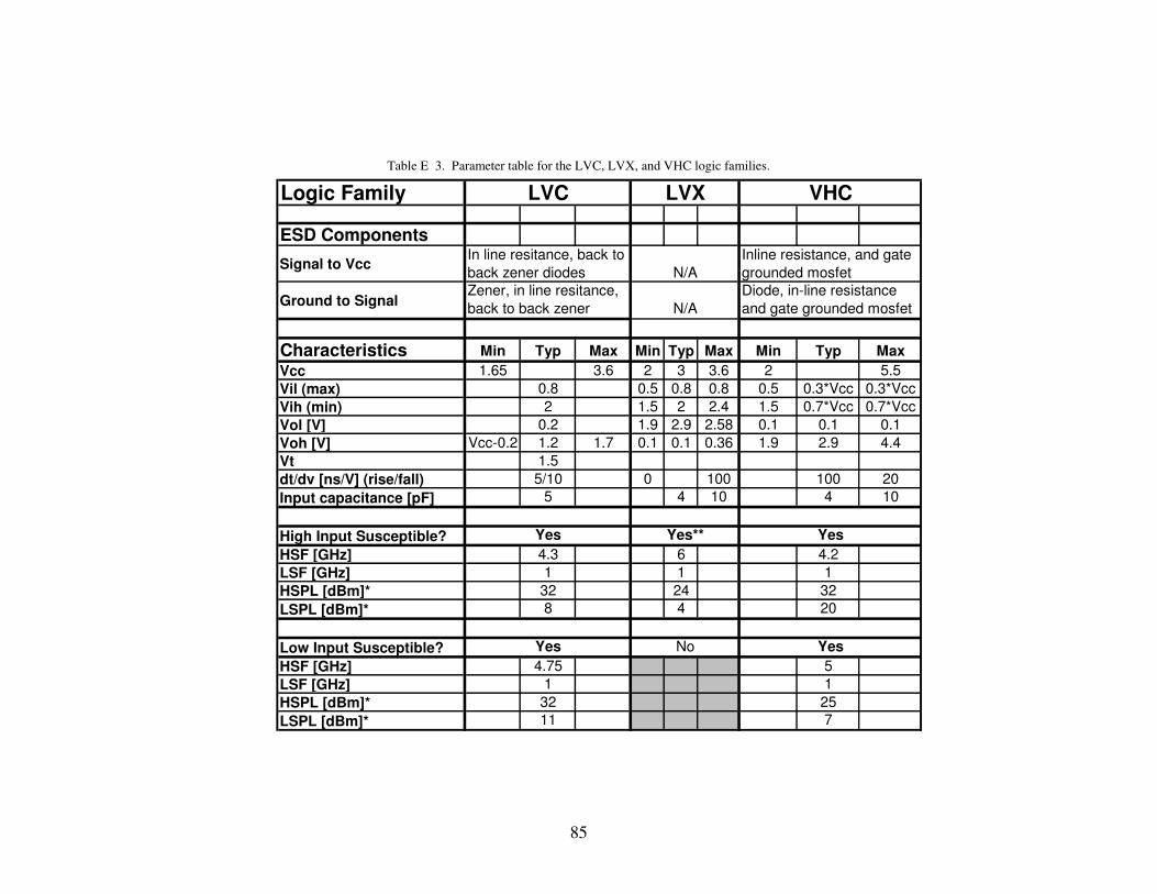
85
Table E 3. Parameter table for the LVC, LVX, and VHC logic families.
Logic Family
ESD Components
Signal to Vcc
Ground to Signal
Characteristics Min Typ Max Min Typ Max Min Typ Max
Vcc 1.65 3.6 2 3 3.6 2 5.5
Vil (max) 0.8 0.5 0.8 0.8 0.5 0.3*Vcc 0.3*Vcc
Vih (min) 2 1.5 2 2.4 1.5 0.7*Vcc 0.7*Vcc
Vol [V] 0.2 1.9 2.9 2.58 0.1 0.1 0.1
Voh [V] Vcc-0.2 1.2 1.7 0.1 0.1 0.36 1.9 2.9 4.4
Vt 1.5
dt/dv [ns/V] (rise/fall) 5/10 0 100 100 20
Input capacitance [pF] 5 4 10 4 10
High Input Susceptible?
HSF [GHz] 4.3 6 4.2
LSF [GHz] 1 1 1
HSPL [dBm]* 32 24 32
LSPL [dBm]* 8 4 20
Low Input Susceptible?
HSF [GHz] 4.75 5
LSF [GHz] 1 1
HSPL [dBm]* 32 25
LSPL [dBm]* 11 7
N/A
N/A
In line resitance, back to
back zener diodes
Zener, in line resitance,
back to back zener
Yes** YesYes
Yes
VHCLVX
No Yes
Inline resistance, and gate
grounded mosfet
Diode, in-line resistance
and gate grounded mosfet
LVC

86
BIBLIOGRAPHY
[1] J. G. Tront, “Predicting URF Upset of MOSFET Digital IC’s”, IEEE Transactions
on Electromagnetic Compatibility, Volume. EMC-27, No. 2, May 1985.
[2] J-J. Laurin, “EMI-Induced Failures in Digital Systems”, University of Toronto,
Toronto, Canada, 1991.
[3] J. G. Sketoe, “Integrated Circuit Electromagnetic Immunity Handbook”, Boeing
Information Space and Defense Systems, Seattle, WA, August 2000.
[4] R. E. Richardson, V. G. Puglielli, R. A. Amadori, “Microwave Interference Effect
in Bipolar Transistors”, IEEE Transactions on Electromagnetic Compatibility,
Volume. EMC-17, No. 4, November 1975.
[5] R. E. Richardson, Jr., “Modeling of Low-Level Rectification RFI in Bipolar
Circuitry”, IEEE Transactions on Electromagnetic Compatibility, Volume. EMC-
21, No. 4, November 1979.
[6] M. L. Forcier and R. E. Richardson, Jr., “Microwave-Rectification RFI Response in
Field-Effect Transistors”, IEEE Transactions on Electromagnetic Compatibility,
Volume. EMC-21, No. 4, November 1979.
[7] R. E. Richardson, Jr., “Quiescent Operating Point Shift in Bipolar Transistor s with
AC Excitation,” IEEE Journal of Solid State Circuits, Volume SC-14, No. 6,
December 1979.
[8] D. J. Kenneally, G. O. Head, and S. C. Anderson, “EMI Noise Susceptibility of
ESD Protect Buffers in Selected MOS Devices”, Procs. IEEE International
Conference on EMC, Wakefield, MA, August 1985.
[9] D. J. Kenneally, D. S. Koellen, S. Epshstein, “RF Upset Susceptibility of CMOS
and Low Power Schottky D-Type, Flip-Flops”, IEEE 1989 National Symposium on
Electromagnetic Compatibility, May 1989.
[10] D. J. Kenneally, D. D. Wilson, S. Epshstein, “RF Upset Susceptibility of CMOS
and Low Power Schottky 4-Bit Comparators”, IEEE 1990 National Symposium on
Electromagnetic Compatibility, August 1990.
[11] P. R. Gray, P. J. Hurst, S. H. Lewis, and R. G. Meyer, “Analysis and Design of
Analog Integrated Circuits”, John Wiley & Sons, Inc., New York, 2001.
[12] S. Marum, Email correspondence, Texas Instruments, March, 2003.

87
[13] Z. Dilli and N. Goldsman, Permission to use this photograph from a MOSIS circuit
of their design, University of Maryland, January, 2004.
[14] S. Dabral, T. Maloney, “Basic ESD and I/O Design”, Wiley, New York, NY, 1998.
[15] D. M. Pozar, “Microwave Engineering”, John Wiley & Sons, Inc., New York,
1998.
[16] R. E. Ziemer, W. H. Tranter, D. R. Fannin, “Signal and Systems – Continuous and
Discrete”, Prentice Hall, Upper Saddle River, NJ, 1998.
[17] R. F. Pierret, “Semiconductor Device Fundamentals”, Addison-Wesley Publishing
Company, Inc., Reading, Massachusetts, March 1996.
[18] R. J. Baker, H. W. Li, and D. E. Boyce, “CMOS circuit design, layout, and
simulation”, IEEE Press, New York, 1997.
[19] R. E. Funk, “Understanding Buffered and Unbuffered CD4xxxB Series –
Application Report SCHA004”, Texas Instruments, 2002.
[20] Haseloff, Eilhard, “Bus-Hold Circuit – Application Report SCLA015”, Texas
Instruments, 2001.
[21] Forstner, Peter, “Low-Voltage-Logic-Families Application Report SCVAE01A”,
Texas Instruments, 1997.
[22] 74LCX04 Low Voltage Hex Inverter with 5V Tolerant Inputs Datasheet Fairchild
Semiconductor, 2001
[23] VHC/VHCT Description and Family Characteristics, Fairchild Semiconductor
1999.
[24] HC/HCT User Guide Production Specification Philips Semiconductor 1997.
[25] “Advanced High-Speed CMOS (AHC) Logic Family Application Report
SCAA034C”, Texas Instruments, 2002.
[26] “LVT (Low Voltage Technology) and ALVT (Advanced LVT) Application Note
AN243”, Philips Semiconductor,1998.
[27] W. Lawler, BICMOS12.slb, MOSIS using the 2.0 micron Orbit process,
http://www.ee.umd.edu/newcomb/bicmosis.htm, March, 1998.
[28] P. Horowitz and W. Hill, “The Art of Electronics”, Cambridge University Press,
New York, 1989.
[29] “Memtest86 - A Stand-alone Memory Diagnostic” http://www.memtest86.com/