accelerator division blm upgrade...
TRANSCRIPT

Accelerator DivisionBLM Upgrade Proposal
Preliminary Testing of the Burr Brown ACF2101
Summary of Test Data
A. BaumbaughK. Knickerbocker
PPD/Electrical Engineering Department
03/23/2004
Fermilab


New BLM Front-end Electronics using the ACF2101 Dual Integrator.
The plan for the new BLM system is to use the Burr-Brown ACF2101 dual integrator,and to “ping-pong” (switch rapidly) between the A and B channels so as to never miss anylosses. The integration times are planned to be 20 µsec minimum. Significant features and adiagram (shown in Figure 1.) of the ACF2101 device are from the Burr-Brown datasheet andgiven below.
DESCRIPTIONThe ACF2101 is a dual switched integrator forprecision applications. Each channel can convertan input current to an output voltage byintegration, using either an internal or externalcapacitor. Included on the chip are precision 100pF integration capacitors, hold and reset switches,and output multiplexers.
FEATURESIncludes Integration Capacitor, Reset and HoldSwitches, and Output MultiplexerLow Noise: 10 µVrmsLow Charge Transfer: 0.1 pCWide Dynamic Range: 120 dBLow Bias Current: 100 fA
Figure 1. The Burr-Brown ACF2101
The ASIC Test System shown in Figure 2 was used as convenient platform forconducting the initial tests of the Burr-Brown dual integrator. The system provided all of thenecessary timing and control signals, plus power supply voltages. It also allowed easycollection and processing of test data on a standard PC.
An existing BLM system daughter card(Beam Line) was obtained from the AcceleratorDivision Instrumentation Department and used forall testing. The card had several modificationsmade to it to make it similar to the new system. Itwas modified to allow the use of both integratorsin the ACF2101 at the same time. The currentBLM system uses one integrator or the other. Thedaughter cards external integration capacitor(1000 pf) was removed and only the internalcapacitors (100 pf) of the ACF2101 were used.Other modifications were made to allow theindividual control of the following signals, ResetA, Reset B, Hold A, Hold B, Track/Hold. The final change made was to the analog powersupply voltages, they were lowered from the standard +15, -15, volts to +12, -12. The +5 voltlogic power supply voltage remained the same.
Figure 2. The ASIC Test System

The different test circuits used are shown in Figures 3, 4, and 5. The current sourceused was a Datel DVC-8500 precision voltage source and a 1.0 Meg ohm metal film leaded orsurface mount resistor. Timing signals for the ACF2101 were provided by a free runningpattern generator available in the ASIC Test System. A 16-Bit ADC available in the ASICtest system was used to make measurements of the integrator output. Figure 3 shows thecurrent source at the far end of 550 ft. of RG-58 cable. Figure 4 shows the current source atthe very input to the two integrators, and Figure 5 shows the cable in parallel with the currentsource. This last mode lets us easily switch between cable and no cable. After some effortwe were able to trigger the ADC in the test system synchronously with the Track and Holdsignal (part of the free running pattern). This allows us to make measurements in exactly thesame way as we are proposing for the new BLM system, although not quite as fast. A timingdiagram for the integrators is shown in Figure 6, we are able to free run both the A and Bchannels, and selectively digitize either A only, B only, or A and B both.
What we found was that the A and B channels have a slightly different input offsetvoltage and input resistance value which causes the two channels to be different. With nocable capacitance this difference is about .04% on a 10µA signal (see Figure 7). However,when a long cable with a large capacitance is attached, the different offset voltages at theinput either charge or discharge the cable as the system “ping-pongs” (for the effect ofdifferent cable lengths see Figure 8). The result is that the A channel reads high byapproximately 200 nA and the B channel reads low by the same amount (Figures 9 and 10).Figure 11 shows the data for reading both A and B sides, note the two separate peaks. Webelieve this to be solely due to the capacitance of the cable and the different offset voltages ofthe two inputs. If we vary the input voltage, (see Figure 12) we also see a slight effect due tothe different input resistor values. The reader should note that the noise in the system has anRMS of 15 counts which is equivalent to and RMS of 3 nA on a 10 µA signal.
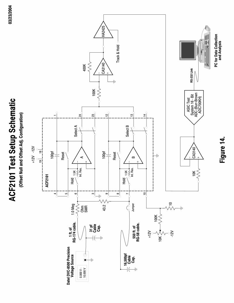
In an effort to reduce or eliminate the differences between the two integrator channelstwo more circuit modification were made. At the suggestion of Craig Drennan an input offsetvoltage nulling circuit was added to the ACF2101. The “Nulling” Circuit, which is bi-polaronly needed to be added to one of the two integrators. This allowed us to adjust the offset ofthe two integrators to be equal at zero input current. This reduced the maximum A-Bdifference from 2000 counts to 859 counts (Figure 13). The remaining effect is the differenceof the “ON” resistance of the two input switches. These switches are about 1.5 kOhm in theON state. By temporarily adding a fixed resistor to A and measuring the shift in A-B, wewere able to calculate the difference of the two switches. The B switch had 43 Ohms lessresistance, by adding a 43 Ohm resistor to the B side we were able to match the twointegrators over a very large range. After adding the nulling circuit and the 43 Ohm resistor(see Fig. 14), we now have matched A-B to –10 to 35 counts (Figure 15) over the entire rangeof 0 to 10 µA. We now believe that we can “Tune” the integrators quite nicely and thuseliminate the need for a cable receiver.
We now have a very nice system for making these measurements and will continue tostudy the front end.

1.0
Meg
Ohm
PC fo
r Dat
a Co
llect
ion
and
Anal
ysis
16,5
00pf
Cabl
eCa
p.
Resi
stor
Box
550
ft. o
fRG
-58
cabl
e.
ACF2
101
Test
Set
up S
chem
atic
03/2
3/20
04
50 Ohm
pf10
0AC
F210
1
0.00
0 V
-10
.000
V
Rese
t
Sele
ct A
A
HP 5
4502
A 40
0 M
Hz D
igita
lO
scill
osco
pe
Hold
pf10
0
Rese
t
Sele
ct B
B
Hold
400K
CA31
40
100K
CA31
4010
K
HA24
25
ASIC
Tes
tSy
stem
16
- Bit
ADC
(Bur
r-Bro
wnAD
C700
KH)
4 5 36 9 8 7 10
+12V
-12V
1918
121 24 23 13 14
Trac
k &
Hold
Date
l DVC
-850
0 Pr
ecis
ion
Volta
ge S
ourc
e1.
5K
Int.
Res.
1.5K
Int.
Res.
RS-2
32 L
ink
(Lon
g Ca
ble
Conf
igur
atio
n)
Figu
re 3
.

PC fo
r Dat
a Co
llect
ion
and
Anal
ysis
31 p
fCa
ble
Cap.
1 ft.
of
RG-1
74 c
able
.
ACF2
101
Test
Set
up S
chem
atic
03/2
3/20
04
1.0
Meg
Ohm
SMR
pf10
0AC
F210
1
0.00
0 V
-10
.000
V
Rese
t
Sele
ct A
A
HP 5
4502
A 40
0 M
Hz D
igita
lO
scill
osco
pe
Hold
pf10
0
Rese
t
Sele
ct B
B
Hold
400K
CA31
40
100K
CA31
4010
K
HA24
25
ASIC
Tes
tSy
stem
16
- Bit
ADC
(Bur
r-Bro
wnAD
C700
KH)
4 5 36 9 8 7 10
+12V
-12V
1918
121 24 23 13 14
Trac
k &
Hold
Date
l DVC
-850
0 Pr
ecis
ion
Volta
ge S
ourc
e1.
5K
Int.
Res.
1.5K
Int.
Res.
RS-2
32 L
ink
(Sur
face
Mou
nt R
esis
tor (
No C
able
) Con
figur
atio
n)
Figu
re 4
.

PC fo
r Dat
a Co
llect
ion
and
Anal
ysis
31 p
fCa
ble
Cap.
1 ft.
of
RG-1
74 c
able
.
ACF2
101
Test
Set
up S
chem
atic
03/2
3/20
04
1.0
Meg
Ohm
SMR
pf10
0AC
F210
1
0.00
0 V
-10
.000
V
Rese
t
Sele
ct A
A
HP 5
4502
A 40
0 M
Hz D
igita
lO
scill
osco
pe
Hold
pf10
0
Rese
t
Sele
ct B
B
Hold
400K
CA31
40
100K
CA31
4010
K
HA24
25
ASIC
Tes
tSy
stem
16
- Bit
ADC
(Bur
r-Bro
wnAD
C700
KH)
4 5 36 9 8 7 10
+12V
-12V
1918
121 24 23 13 14
Trac
k &
Hold
Date
l DVC
-850
0 Pr
ecis
ion
Volta
ge S
ourc
e1.
5K
Int.
Res.
1.5K
Int.
Res.
RS-2
32 L
ink
(Sur
face
Mou
nt R
esis
tor (
Opt
iona
l Cab
le) C
onfig
urat
ion)
Figu
re 5
.
16,5
00pf
Cabl
eCa
p.55
0 ft.
of
RG-5
8 ca
ble.
Jum
per

Zoom
Clo
ck n
S
R1
=R
2 =
R2
- R1
=
Sel A
Bit
- 4
Sel B
Bit
- 5
Unu
sed
Hol
d A
Bit
- 0
Res
et A
Bit
- 2
T/H
A O
nly
Bit
- 6
Unu
sed
Hol
d B
Bit
- 1
Res
et B
Bit
- 3
T/H
B O
nly
Bit
- 7
Unu
sed
T/H
AB
Bit
- 8
Unu
sed
Unu
sed
AD
C B
usy
Bit
- 9
Unu
sed
C:\N
anoS
im\N
SM\B
LM_T
est.N
SM
-.42
-.42
.00
T1 =
T2 =
T2 -T
1 =
110 25

5100
051
020
5104
051
060
5108
051
100
5112
051
140
0
100
200
300
400
500
600
700
800
900
1000
Mea
n =
5107
1.86
5S
td. D
ev. =
14.
290
Num
. Sam
ples
= 4
096
Inpu
t = 1
0.00
0 V
Counts
5100
051
020
5104
051
060
5108
051
100
5112
051
140
0
100
200
300
400
500
600
700
800
900
1000
Mea
n =
5106
1.45
7S
td. D
ev. =
9.1
13N
um. S
ampl
es =
409
6In
put =
10.
000
V
Counts
5100
051
020
5104
051
060
5108
051
100
5112
051
140
0
100
200
300
400
500
600
700
800
900
1000
Figu
re 7
.
Mea
n =
5108
5.50
6S
td. D
ev. =
9.0
38N
um. S
ampl
es =
409
6In
put =
10.
000
V
Counts
Ch.
A, B
, A&
B, N
o C
able
/1 M
eg S
MR
, Inp
ut 1
0.00
0V, S
ync
AD
C, (
File
s: B
LM_X
X_SM
R_1
0000
.DA
T)

Cha
nnel
A a
nd B
plo
tted
with
diff
eren
t len
gths
of c
oaxi
al c
able
(RG
-58)
atta
ched
.
Red
, Cab
le L
engt
h =
550
ft., B
lue,
Cab
le L
engt
h =
1 ft.
, Gre
en, C
able
Len
gth
= 0
ft.
Figu
re 8
.

5212
052
140
5216
052
180
5220
052
220
5224
052
260
5228
052
300
5232
00
100
200
300
400
500
600
700
Figu
re 9
.
Mea
n =
5218
8.56
1S
td. D
ev. =
15.
405
Num
. Sam
ples
= 4
096
Inpu
t = 1
0.00
0 V
Counts
Ch.
A, 5
50 ft
. Cab
le, I
nput
10
+ .0
00V,
.010
V, .0
11V,
Syn
c A
DC
, (Fi
les:
BLM
_A_L
_100
XX.D
AT)
5212
052
140
5216
052
180
5220
052
220
5224
052
260
5228
052
300
5232
00
100
200
300
400
500
600
700
Mea
n =
5224
0.03
1S
td. D
ev. =
15.
731
Num
. Sam
ples
= 4
096
Inpu
t = 1
0.01
0 V
Counts
5212
052
140
5216
052
180
5220
052
220
5224
052
260
5228
052
300
5232
00
100
200
300
400
500
600
700
Bin
Siz
e =
5
Mea
n =
5224
6.03
5S
td. D
ev. =
15.
543
Num
. Sam
ples
= 4
096
Inpu
t = 1
0.01
1 V
Counts

5086
050
880
5090
050
920
5094
050
960
5098
051
000
5102
00
100
200
300
400
500
600
700
Mea
n =
5096
7.07
8S
td. D
ev. =
14.
928
Num
. Sam
ples
= 4
096
Inpu
t = 1
0.01
1 V
Counts
5086
050
880
5090
050
920
5094
050
960
5098
051
000
5102
00
100
200
300
400
500
600
700
Mea
n =
5097
0.99
1S
td. D
ev. =
14.
771
Num
. Sam
ples
= 4
096
Inpu
t = 1
0.01
0 V
Counts
5086
050
880
5090
050
920
5094
050
960
5098
051
000
5102
00
100
200
300
400
500
600
700
Figu
re 1
0.
Mea
n =
5091
4.74
7S
td. D
ev. =
14.
872
Num
. Sam
ples
= 4
096
Inpu
t = 1
0.00
0 V
Counts
Ch.
B, 5
50 ft
. Cab
le, I
nput
10
- .00
0V, .
010V
, .01
1V, S
ync
AD
C, (
File
: BLM
_B_L
_100
XX.D
AT)

5080
051
000
5120
051
400
5160
051
800
5200
052
200
5240
00
100
200
300
400
500
600
Figu
re 1
1.
Mea
n =
5217
8.64
0S
td. D
ev. =
15.
052
Num
. Sam
ples
= 2
059
Bin
Siz
e =
10
Mea
n =
5092
6.85
2S
td. D
ev. =
15.
200
Num
. Sam
ples
= 2
037
Counts
Ch.
A&
B, 5
50 ft
. Cab
le, I
nput
10.
000V
, Syn
c A
DC
, (Fi
le: B
LM_A
B_L
_100
00.D
AT)

1960
019
800
2000
020
200
2040
020
600
2080
021
000
2120
021
400
2160
00
100
200
300
400
500
600
Bin
Siz
e =
10
Mea
n =
2149
3.85
1S
td. D
ev. =
15.
009
Num
. Sam
ples
= 2
016
Mea
n =
1976
7.41
6S
td. D
ev. =
15.
118
Num
. Sam
ples
= 2
080
Counts
Ch.
A&
B, 5
50 ft
. Cab
le, I
nput
4.0
00V,
Syn
c AD
C, (
File
: BLM
_AB
_L_4
V.D
AT)
3000
030
200
3040
030
600
3080
031
000
3120
031
400
3160
031
800
3200
00
100
200
300
400
500
600
Bin
Siz
e =
10
Mea
n =
3171
7.32
3S
td. D
ev. =
14.
639
Num
. Sam
ples
= 1
982
Mea
n =
3015
0.46
8S
td. D
ev. =
14.
825
Num
. Sam
ples
= 2
114
Counts
Ch.
A&
B, 5
50 ft
. Cab
le, I
nput
6.0
00V,
Syn
c AD
C, (
File
: BLM
_AB
_L_6
V.D
AT)
4020
040
400
4060
040
800
4100
041
200
4140
041
600
4180
042
000
4220
00
100
200
300
400
500
600
Bin
Siz
e =
10
Mea
n =
4194
8.08
5S
td. D
ev. =
14.
997
Num
. Sam
ples
= 2
074
Mea
n =
4053
8.63
1S
td. D
ev. =
15.
332
Num
. Sam
ples
= 2
022
Counts
Ch.
A&
B, 5
50 ft
. Cab
le, I
nput
8.0
00V,
Syn
c AD
C, (
File
: BLM
_AB
_L_8
V.D
AT)
9200
9400
9600
9800
1000
010
200
1040
010
600
1080
011
000
1120
011
400
0
100
200
300
400
500
600
Figu
re 1
2.
Bin
Siz
e =
10
Mea
n =
1127
1.24
3S
td. D
ev. =
14.
524
Num
. Sam
ples
= 2
065
Mea
n =
9379
.528
Std
. Dev
. = 1
4.82
8N
um. S
ampl
es =
203
1
Counts
Ch.
A&
B, 5
50 ft
. Cab
le, I
nput
2.0
00V,
Syn
c AD
C, (
File
: BLM
_AB
_L_2
V.D
AT)

0 2 4 6 8 10
1500
1550
1600
1650
1700
1750
0 2 4 6 8 100
200
400
600
800
1000
Ch. A-B Data Difference vs. Input Current, No CompensationC
h. A
-B in
AD
C C
ount
s
Input Current in microAmps
Figure 13.
Ch. A-B Data Difference vs. Input Current, Long Cable, Nulled at 0V
Ch.
A-B
in A
DC
Cou
nts
Input Current in microAmps
PC fo
r Dat
a Co
llect
ion
and
Anal
ysis
31 p
fCa
ble
Cap.
1 ft.
of
RG-1
74 c
able
.
ACF2
101
Test
Set
up S
chem
atic
03/2
3/20
04
1.0
Meg
Ohm
SMR
pf10
0AC
F210
1
0.00
0 V
-10
.000
V
Rese
t
Sele
ct A
A
Hold
pf10
0
Rese
t
Sele
ct B
B
Hold
400K
CA31
40
100K
CA31
4010
K
HA24
25
ASIC
Tes
tSy
stem
16
- Bit
ADC
(Bur
r-Bro
wnAD
C700
KH)
4 5 36 9 8 7 10
+12V
-12V
1918
121 24 23 13 14
Trac
k &
Hold
Date
l DVC
-850
0 Pr
ecis
ion
Volta
ge S
ourc
e1.
5K
Int.
Res.
1.5K
Int.
Res.
RS-2
32 L
ink
(Offs
et N
ull a
nd O
ffset
Adj
. Con
figur
atio
n)
Figu
re 1
4.
16,5
00pf
Cabl
eCa
p.55
0 ft.
of
RG-5
8 ca
ble.
Jum
per
100K
10
+12V
-12V
10K
43.2

02
46
810
-10010203040
Figu
re 1
5.
Ch.
A-B
Dat
a D
iffer
ence
vs.
Inpu
t, Lo
ng C
able
, Nul
led
at 0
V, R
esis
tor C
ompe
nsat
edCh. A-B in ADC Counts
Inpu
t Cur
rent
in m
icro
Am
ps

Datasheets:
Texas Instruments/Burr-Brown, - ACF2101, Low Noise, Dual Switched Integrator.PDS-1078D (SBFS003) http://www.burr-brown.com/
Texas Instruments/Burr-Brown, - Improved Noise Performance of the ACF2101Switched Integrator., Application Bulletin AB-053 (SBOA032) http://www.burr-brown.com/
Intersil, - HA-2420, HA-2425, Sample and Hold Amplifier., (FN2856.4)http://www.intersil.com/
Harris Semiconductor, - CA3140, CA3140A, 4.5 MHz, BiMOS Operational Amplifierwith MOSFET Input/Bipolar Output., (File Number 957.3) http://www.harris.com/
Acknowledgements:
We would like to thank the following people for their assistance during the testing ofthe ACF2101: Craig Drennan for circuit suggestions, ideas, and advice. Marvin Olson forthe loan of a BLM daughter card, ACF2101 devices, and 550 ft. of coaxial cable. AndCharlie Nelson for circuit suggestions, ideas, and advice.