acceptor made of a small-molecule donor and polymer a ... jahandar,b,c shafket rasool,a,c chang eun...
TRANSCRIPT

1
Electronic Supplementary Material (ESI) for Journal of Materials Chemistry A
A Thermally and Mechanically Stable Solar Cell Made of a Small-Molecule Donor and Polymer
AcceptorSora Oh,a,c† Sachin Badgujar,a† Da Hun Kim,b,c Wang-Eun Lee,c,d Nasir Khan,b,c Muhammad Jahandar,b,c Shafket Rasool,a,c Chang Eun Song,*,b,c Hang Ken Lee,b Won Suk Shin,b,c Jong-Cheol Lee,a,c Sang-Jin Moon,b,c and Sang Kyu Lee,*,a,c
aAdvanced Materials Division, Korea Research Institute of Chemical Technology (KRICT), 141 Gajeongro, Yuseong, Daejeon 34114, Republic of Korea. E-mail: [email protected] of Solar Energy Materials, Korea Research Institute of Chemical Technology (KRICT), 141 Gajeongro, Yuseong, Daejeon 34114, Republic of Korea. E-mail: [email protected] Materials and Chemical Engineering, University of Science and Technology (UST), 217 Gajeongro, Yuseong, Daejeon 34113, Republic of Korea.dReliability Assessment Center for Chemical Materials, Korea Research Institute of Chemical Technology (KRICT), 141 Gajeongro, Yuseong, Daejeon 34114, Republic of Korea.
† These authors contributed equally.
Correspondence and requests for materials should be addressed to C.E.S. (email: [email protected]) or to S.K.L. (email: [email protected]).
Electronic Supplementary Material (ESI) for Journal of Materials Chemistry A.This journal is © The Royal Society of Chemistry 2017

2
Experimental Sections
Instruments
UV-vis absorption measurements were recorded using double-beam Shimadzu UV–2550
(wavelength range 300–900 nm). The thickness and roughness of films were examined with
an Alpha-Step IQ surface profiler (KLA Tencor). The atomic force microscope (AFM)
(Multimode IIIa, Digital Instruments) was operated in tapping mode to acquire images of the
surfaces of films. Cross-sectional TEM image of thick devices were acquired by iusing a Helios
dual Beam FIB. Conventional transmission electron microscopy (TEM) was performed using a
JEOL JEM-2200FS. FE-SEM was performed on Tescan Mira 3 LMU FEG operated at 20 kV. X-
ray photoelectron was performed on AXIS Nova (150 W, monochromatic Al-Kα, 40 eV). The
J-V characteristics of relevant devices were measured by using a computer-controlled
Keithley 236 source measure unit.
Materials
All chemicals and solvents were purchased from Aldrich and were used without further
purification. The materials BDT2TR was synthesized by this literature1, PC71BM and PNDI-2T
were purchased from EM-Index and one-materials, respectively.
Fabrication of the Organic solar cells (OSCs)
In this study, the devices were fabricated with the structure ITO/PEDOT:PSS/ BDT2TR small
molecule donor:PC71BM or PNDI-2T acceptor/Ca/Al. The procedure for cleaning the ITO
surface included sonication and rinsing in deionized water, methanol, and acetone. The
PEDOT:PSS (~35nm) film as a hole transport layer was spin-coated onto each ITO anode from
a solution purchased from H. C. Starck (AI 4083). For deposition of the active layer, blend
solutions of BDT2TR:PC71BM, BDT2TR:PNDI-2T (1.0:1.0 w/w, 15 mg, filtered by 0.45µm)
dissolved in chloroform (1 mL) were spin-cast (at 2000 r.p.m.) on top of the PEDOT:PSS layer.

3
The optimized thickness of active layer was ~ 100nm. From thicker to thinner films were
produced by varying the solution concentration and spin rate from total 1.2 to 3.0 wt% and
from 600 to 4000 r.p.m. After the deposition of photo-active layers all substrates were dried
on hot plate for 10min at 100 oC. Calcium and aluminum contacts were formed by vacuum
deposition at pressures below 3 x 10⁻⁶ Torr, providing an effective active area of 0.09 cm2.
Solar cell efficiencies were characterized under simulated 100 mW/cm2 AM 1.5G irradiation
from a Xe arc lamp with an AM 1.5 global filter. Simulator irradiance was characterized using
a calibrated spectrometer, and the illumination intensity was set using an NREL-certified
silicon diode with an integrated KG1 optical filter. The EQE was measured by underfilling the
device area using a reflective microscope objective to focus the light output from a Xenon
lamp outfitted with a monochromator and optical chopper; the photocurrent was measured
using a lock-in amplifier, and the absolute photon flux was determined using a calibrated
silicon photodiode. All device fabrication procedures and measurements were carried out in
air at room temperature.
Solar cell stability
Thermal stability test: all devices fabricated as follow organic solar cell fabrication process.
But before deposition of top electrode (Ca/Al), the films were placed on the hotplate in N2
filled glove box (isolating the effects of moisture, oxygen and light) at various temperatures
(100 oC, 150 oC and 250 oC). After thermal stress, Calcium and aluminum contacts were
formed by vacuum deposition at pressures below 3 x 10⁻⁶ Torr. All device fabrication
procedures and measurements were carried out in air at room temperature.
Device fabrication for light and air stability: the inverted device structure is employed with
indium tin oxide (ITO)/zinc oxide (ZnO)/polyethylenimine ethoxylated (PEIE)/photo-active
layer (d = ~100 nm)/molybdenum oxide(MoO3)/Ag for the light and air stability test. Glass

4
substrates were used with pre-patterned ITO. These were cleaned by sonication in detergent,
deionized water, acetone and isopropanol in the sonication bath. ZnO (sol-gel or NPs) layers
were deposited by spin coating of the respective solution followed by annealing at 150 oC for
10~15 min, giving layers of 30 nm thickness. The photo-active layers (d = ~100nm) were
deposited from 15mg ml-1 solutions in chloroform (1mL) by spin coating at 2,000 r.p.m. Top
electrode of the MoOX (10 nm) and Ag (100 nm) layers were deposited by thermal
evaporation at pressures below 3 x 10⁻⁶ Torr.
Photostability test: all devices with glass to glass encapsulation were stored in a humidity
and temperature control chamber equipped with a sulfur plasma lamp and a computer-
controlled voltage source measure unit for in situ current density–voltage (J–V)
measurements. For the photodegradation test, the samples were exposed to light of
intensity∼ 100 mW cm–2 from the sulfur plasma lamp in air for 200 h. These conditions were
applied for all photodegradation treatments used in this work. All samples were illuminated
through the ITO. Devices were always stored at short-circuit except during periodic J–V scans.
J–V scans at predetermined intervals were controlled by a computer program and resulting
values for JSC, VOC, FF were automatically recorded. The light intensity of ∼ 100 mW cm–2 was
estimated by measuring the photocurrent from a silicon photodiode and assuming AM 1.5
spectral distribution. However, as the illumination spectrum is not the same as the AM 1.5
solar spectrum, we present the performance parameters during degradation after
normalizing to their initial values.
Air stability: The air stability of BDT2TR:PC71BM and BDT2TR:PNDI-2T devices was studied by
keeping them out of the glove box without encapsulation. Devices were stored at room
temperature, under the dark for 10 days.
SCLC devices fabrication and testing

5
Mobility measurements of oligomer/PC71BM (w/w, 1.0:1.0), and oligomer:PNDI-2T blends
were done by a charge-only space-charge limited current (SCLC) method with the following
diode structures: ITO/PEDOT:PSS/active layer/Au for hole-only devices and ITO/ZnO
NPs/active layer/Ca/Al for electron-only devices by taking current-voltage measurements
and fitting the results to a space-charge limited form. The charge carrier mobilities were
calculated using the SCLC model, where the SCLC is described by: 9ε0εrµV2/8L3, where J is the
current density, L is the film thickness of the active layer, μ0 is the hole or electron mobility,
εr is the relative dielectric constant of the transport medium, ε0 is the permittivity of free
space (8.85 × 10⁻¹² F m–1), V is the internal voltage in the device, and V = Vappl – Vr – Vbi,
where Vappl is the applied voltage to the device, Vr is the voltage drop due to contact
resistance and series resistance between the electrodes, and Vbi is the built-in voltage due to
the relative work function difference of the two electrodes.
Synchroton X-ray Diffraction Analysis
Grazing-incidence XRD (GIXD) measurements were conducted at PLS-II 9A U-SAXS beamline
of Pohang Acceleartor Laboratory (PAL) in Korea. The X-rays coming from the in-vacuum
undulator (IVU) are monochromated using Si(111) double crystals and focused at the
detector position using K-B type mirrors. GIXD patterns were recorded with a 2D CCD
detector (Rayonix SX165) and X-ray irradiation time was 2 ~ 120 seconds dependent on the
saturation level of detector. Diffraction angles were calibrated by a pre-calibrated sucrose
(Monoclinic, P21, a = 10.8631 Å, b = 8.7044 Å, c = 7.7624 Å, b = 102.938o) and the sample-
to-detector distance was about 223.2 mm.
Flexible device fabrication
PET/ITO substrates were used for flexible devices. After spin coating PEDOT:PSS on PET/ITO
substrate at 4000 rpm for 60 s, the samples were dried on hotplate at 100 oC for 20 min. The

6
active area was fixed at 0.16 cm2. All devices fabrication except Ca/Al (~100 nm) deposition
and measurement was conducted at air condition under controlled relative humidity below
35 %.
Photoluminescence (PL) spectroscopy
Thin films were excited at 600 nm or 400nm with a solid state laser in continuous wave
operation (MGL-III-532, Changchun New Industries) at an excitation power of 80 mW. The
laser beam was expanded to a spot size of 6 mm in diameter in order to probe a rather large
sample volume. Photoluminescence was fiber-coupled into a spectrograph (Acton Research
SpectraPro 300i) and detected with an intensified CCD (Princeton Research, PiMax 512). The
thickness of all films is identical for accuracy of the PL quenching efficiency.
1 S. Badgujar, G.-Y. Lee, T. Park, C. E. Song, S. Park, S. Oh, W. S. Shin, S.-J. Moon, J.-C. Lee, S. K. Lee, Adv. Energy
Mater., 2016, 6, 1600228.
2. S. A. Gevorgyan, M. Jørgensen and F. C. Krebs, Sol. Energy Mater. Sol. Cells, 2008, 92, 736.

7
Fig. S1 DSC thermogram of (a) PC71BM and (b) PNDI-2T in a N2 atmosphere at scan rate of 10 oC min-1.
Fig. S2 PL spectra of neat PNDI-2T and blend in film state with excitation wavelength at 400 nm.

8
Fig. S3 2D GIWAXS image of pristine film of (a) BDT2TR, (b) PC71BM, (c) PNDI-2T.
Fig. S4 Line-cuts profiles from neat of BDT2TR, PC71BM, and PNDI-2T film, and blend of two film corresponding (a) out-of-plane, (b) in-plane.

9
Fig. S5 The J-V curve of BDT2TR:PNDI-2T OSCs with different active layer blend ratios.
Fig. S6 The dark J-V curve of (a) hole-only and (b) electron-only device based on the BDT2TR:PC71BM, BDT2TR:PNDI-2T blend film with annealing time, Dark J-V properties of (c) BDT2TR:PC71BM OSCs with different thermal stability processing of 0 h, 2 h, and 15 h, (d) BDT2TR:PNDI-2T OSCs with different thermal stability processing of 0 h, 2 h, and 15 h.

10
Fig. S7 J–V curves of OSCs based on (a) BDT2TR:PC71BM (b) BDT2TR:PNDI-2T processed with without thermal stress, (b), (e) with thermal processing at 150 oC for 2h, (c),(f) at 150 oC for 15 h under a light intensity of 3.2~100 mW cm-2.
Fig. S8 J–V curves of OSCs based on (a) BDT2TR:PC71BM (b) BDT2TR:PNDI-2T processed with thermal stress at 100 oC (c) solar cell performance thermal stability at 100 oC based on the BDT2TR:PC71BM (filled) and BDT2TR:PNDI-2T device (unfilled).

11
Fig. S9 J–V curves of OSCs based on a BDT2TR:PC71BM (filled) and BDT2TR:PNDI-2T (unfilled) processed with thermal stress at 250 oC.
Fig. S10 (a) The J–V curves and (b) EQE spectra of inverted device of initial performance of BDT2TR:PC71BM, and BDT2TR:PNDI-2T from different ZnO (sol-gel & NPs) for light stability test.
12
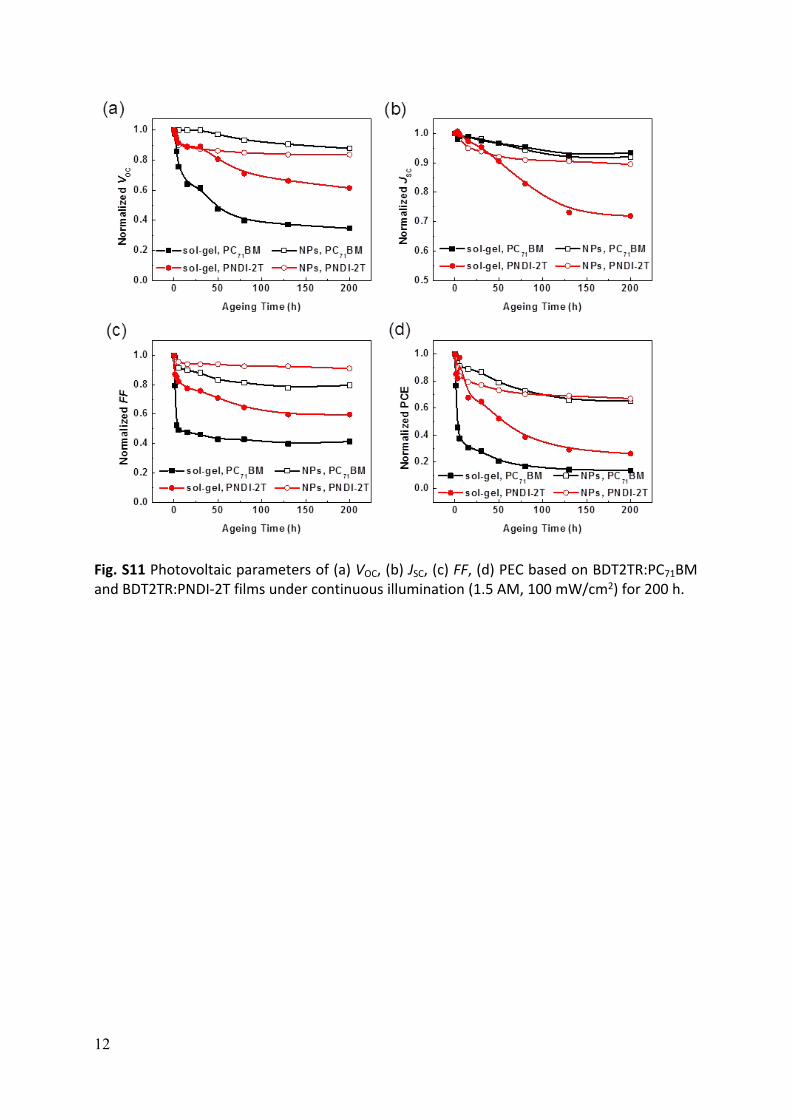
Fig. S11 Photovoltaic parameters of (a) VOC, (b) JSC, (c) FF, (d) PEC based on BDT2TR:PC71BM and BDT2TR:PNDI-2T films under continuous illumination (1.5 AM, 100 mW/cm2) for 200 h.

13
Fig. S12 The J–V curves of BDT2TR:Acceptor device from (a) PC71BM, (b) PNDI-2T. Inverted devices are ITO/sol-gel ZnO/BDT2TR:Acceptor/MoOX/Ag and stored in the dark under ambient conditions for 10 days.
Fig. S13 The J–V curves of BDT2TR:PC71BM device from different ZnO (a) sol-gel, (b) NPs. Devices were stored in the dark under ambient conditions for 10 days.

14
Fig. S14 The J-V curve of (a) BDT2TR:PC71BM (b) BDT2TR:PNDI-2T OSCs with different active layer thickness.

15
Fig. S15 The cross-section TEM imaged of (a) BDT2TR:PC71BM OSCs with 360nm active layer thickness (b) BD2TR:PNDI-2T OSCs with 610nm active layer thickness.

16
Fig. S16 The surface profile of the relevant bending test based on BDT2TR:PC71BM and BDT2TR:PNDI-2T OSCs with different bending radius per each 100 cycles.

17
Table S1. Packing parameters od pristin active materials and blen two OSCs derived from GIWXS measurements.
Active Layer Component(100) dlamellar
[Å]a
(010) dπ-π
[Å]a
(100) dlamellar
[Å]b
(010) dπ-π
[Å]b
BDT2TR - 22.21 - 20.41 3.55
PNDI-2T - - 4.03 24.37 -
BDT2TR:PC71BM - 22.96 - 20.65 3.58
BDT2TR 23.60 - 21.30 -BDT2TR:PNDI-2T
PNDI-2T - 3.77 24.73 -
aCalculation from z-axis.bCalculation from xy-axis.
Table S2. Device characteristics BDT2TR:PNDI-2T OSCs with different D:A blend ratios under conventional device architecture ITO/PEDOT:PSS/Photo-active layer/Ca/Al.
Wight ratio
[w/w]VOC [V] JSC [mA/cm2] FF [%] PCE [%]
1.0:0.5 0.85 6.61 68 3.83
1.0:0.8 0.86 6.68 69 3.96
1.0:1.0 0.86 7.26 71 4.43
1.0:1.5 0.85 6.29 69 3.75

18
Table S3 Photovoltaic properties of the BDT2TR:PC71BM and BDT2TR:PNDI-2T device under thermal stress at 100 oC for 24 h in N2 filled glove box.
AcceptorTime
[h]
VOC
[V]
JSC
[mA/cm2]
FF
[%]
PCEa
[%]
0 0.87 13.03 72 8.17 (8.03)b
1 0.86 12.84 71 7.81 (7.70)b
2 0.85 12.76 70 7.59 (7.42)b
5 0.83 12.69 67 7.03 (6.89)b
10 0.82 12.53 65 6.68 (6.40)b
15 0.82 12.51 65 6.62 (6.34)b
PC71BM
24 0.81 12.09 63 6.14 (5.95)b
0 0.85 7.10 72 4.35 (4.24)b
1 0.85 7.05 72 4.30 (4.22)b
2 0.85 6.97 72 4.24 (4.14)b
5 0.84 7.01 72 4.26 (4.18)b
10 0.84 7.02 72 4.28 (4.19)b
15 0.84 7.04 72 4.26 (4.16)b
PNDI-2T
24 0.84 7.00 72 4.24 (4.12)b
aThe device architecture is ITO/PEDOT:PSS/BDT2TR:Acceptor(d = ~100nm)/Ca/Al.bThe average PCE in the brackets is obtained from over 5 independent devices.

19
Table S4 Photovoltaic properties of a BDT2TR:PC71BM and BDT2TR:PNDI-2T device under thermal stress at 250 oC.
AcceptorTime
[min]
VOC
[V]
JSC
[mA/cm2]
FF
[%]
PCEa
[%]
0 0.90 12.62 72 8.20 (8.11)a
10 0.71 4.01 32 0.91 (0.82)aPC71BM
30 0.03 0.00 00 0.00 (0.00)a
0 0.86 7.26 71 4.43 (4.30)a
10 0.67 4.04 37 0.99 (0.89)aPNDI-2T
30 0.01 0.00 00 0.00 (0.00)a
aThe device architecture is ITO/PEDOT:PSS/BDT2TR:Acceptor(d = ~100nm)/Ca/Al.bThe average PCE in the brackets is obtained from over 5 independent devices.

20
Table S5 The initial photovoltaic properties of a BDT2TR:PC71BM and BDT2TR:PNDI-2T device with different ZnO conditions for light stability test.
Acceptor ZnOVOC
[V]
JSC
[mA/cm2]
FF
[%]
PCEa
[%]
sol-gel 0.81 12.96 (12.54)b 67 7.04 (6.58)c
PC71BMNPs 0.77 12.55 (12.23)b 64 6.13 (5.02)c
sol-gel 0.88 6.13 (6.08)b 73 3.93 (3.85)c
PNDI-2TNPs 0.87 6.16 (6.07)b 71 3.78 (3.49)c
aThe device architecture is ITO/ETL/PEIE/BDT2TR:Acceptor(d = ~100nm)/MoOX/Ag.bThe value is calculated from EQE data.cThe average PCE in the brackets is obtained from over 5 independent devices.

21
Table S6 The photovoltaic properties of a BDT2TR:PC71BM and BDT2TR:PNDI-2T device with sol-gel ZnO. Devices were stored in the dark under ambient conditions for 10 days.
AcceptorTime
[day]
VOC
[V]
JSC
[mA/cm2]
FF
[%]
PCE
[%]
0.0 0.80 13.00 67 7.02
0.5 0.80 12.91 67 6.95
1.0 0.80 12.92 67 6.92
2.0 0.80 12.90 67 6.87
4.0 0.80 12.79 67 6.85
7.0 0.81 12.70 67 6.82
PC71BM
10.0 0.80 12.65 67 6.76
0.0 0.87 6.46 70 3.92
0.5 0.86 6.41 70 3.85
1.0 0.86 6.37 70 3.83
2.0 0.86 6.35 70 3.80
4.0 0.86 6.26 70 3.77
7.0 0.87 6.12 71 3.77
PNDI-2T
10.0 0.87 6.09 71 3.73
aThe device architecture is ITO/sol-gel ZnO/PEIE/BDT2TR:Acceptor(d = ~100nm)/MoOX/Ag.

22
Table S7 The photovoltaic properties of a BDT2TR:PC71BM and BDT2TR:PNDI-2T device with ZnO NPs. Devices were stored in the dark under ambient conditions for 10 days.
AcceptorTime
[day]
VOC
[V]
JSC
[mA/cm2]
FF
[%]
PCE
[%]
0.0 0.79 12.47 64 6.29
0.5 0.79 12.39 64 6.24
1.0 0.78 12.34 63 6.15
2.0 0.78 12.27 64 6.13
4.0 0.78 12.28 64 6.11
7.0 0.79 12.29 63 6.12
PC71BM
10.0 0.78 12.32 63 6.08
0.0 0.87 6.20 70 3.77
0.5 0.87 6.16 70 3.76
1.0 0.86 6.16 71 3.78
2.0 0.86 6.18 70 3.76
4.0 0.87 6.14 70 3.72
7.0 0.87 6.11 70 3.73
PNDI-2T
10.0 0.86 6.10 70 3.68
aThe device architecture is ITO/ZnO NPs/PEIE/BDT2TR:Acceptor(d = ~100nm)/MoOX/Ag.

23
Table S8. Conventional OSCs results of BDT2TR:PC71BM and BDT2RT:PNDI-2T with variable film thickness.
Acceptor d [nm] VOC [V] JSC [mA/cm2] FF [%] PCE [%]
~360 0.88 14.16 48 6.04 (5.83)a
~320 0.88 14.16 56 6.99 (6.80)a
~270 0.89 14.13 61 7.67 (7.47)a
~220 0.89 13.46 63 7.59 (7.38)a
~160 0.89 12.18 65 7.08 (6.81)a
~100 0.90 12.62 72 8.20 (8.11)a
PC71BM
~80 0.91 12.43 70 7.91 (7.77)a
~610 0.86 6.18 69 3.67 (3.60)a
~500 0.87 6.89 69 4.12 (4.02)a
~400 0.86 6.75 69 4.04 (3.90)a
~340 0.86 6.72 70 4.05 (3.90)a
~240 0.88 7.01 70 4.28 (4.14)a
~160 0.87 6.76 70 4.12 (4.03)a
~100 0.86 7.26 71 4.43 (4.30)a
PNDI-2T
~80 0.88 6.96 70 4.29 (4.18)a
aThe average PCE in the brackets is obtained from over 5 independent devices.

24
Table S9. Photovoltaic properties of of BDT2RT:PC71BM and BDT2RT:PNDI-2T OSCs with various bending radius.
AcceptorBending
radius
VOC
[V]
JSC
[mA/cm2]
FF
[%]
PCE
[%]
Infinite 0.90 12.57 65 7.33 (6.98)a
140 mm 0.89 10.64 58 5.52 (5.13)a
100 mm 0.88 9.70 52 4.43 (3.78)a
PC71BM
80 mm 0.43 9.67 38 1.59 (0.99)a
Infinite 0.87 7.26 63 3.99 (3.71)a
140 mm 0.87 7.16 61 3.81 (3.30)a
100 mm 0.86 7.06 60 3.65 (3.22)aPNDI-2T
80 mm 0.86 6.09 61 3.20 (3.04)a
aThe average PCE in the brackets is obtained from over 5 independent devices.