accident identification using gps and gsm technology
DESCRIPTION
Full Report on the Topic "Accident Identification using GSM and GPS technology"TRANSCRIPT
VISVESVARAYA TECHNOLOGICAL UNIVERSITY “Jnana Sangama”, Belgaum-590014
Project Report on
“ACCIDENT IDENTIFICATION USING GSM AND
GPS TECHNOLOGY”
Submitted in partial fulfillment of the requirements for the award of degree of
BACHELOR OF ENGINEERING IN
ELECTRONICS AND COMMUNICATION ENGINEERING
By:
GURURAJA HEGDE V CHANDRAKANTH.H
(1GS09EC011) (1GS09EC007)
TOUSIF PASHA
(1GS09EC036)
Under the guidance of Mr. ASHOKA.A
Asst. Professor, Dept. of ECE, GSSIT.
Department of Electronics and Communication Engineering

G S S Institute of Technology #37/2, Komaghatta, New Byrohalli Road, Kengeri Upanagara, Bangalore-560060
Department of Electronics and Communication Engineering
CERTIFICATE
Certified that the Seminar work entitled “ACCIDENT IDENTIFICATION USING
GSM AND GPS TECHNOLOGY ”carried out by Mr. GURURAJA HEGDE V
[1GS09EC011],Mr. CHANDRAKANTH.H [1GS09EC007], Mr. TOUSIF PASHA
[1GS09EC036] a bonafide students of Eight Semester B. E. in the Department of Electronics and Communication Engineering, G S S I T, in partial fulfillment for the
award of Bachelor of Engineering in Electronics and Communication Engineering of the Visvesvaraya Technological University, Belgaum during the academic year 2012-2013. It
is certified that all corrections/suggestions indicated for Internal Assessment have been incorporated in the seminar report deposited in the department library. The seminar report has been approved as it satisfies the academic requirements in respect of Seminar work
prescribed for the said degree.
Signature of the Guide Mr. Ashoka A
Signature of the HOD
Mr. Krishnananda
External Viva Voice
Signature of the Principal
Dr. Vidyashankar. B. V
Name of the Examiners Signature with date
1.
2.

i
ACKNOWLEDGMENT
Numerous personalities, directly or indirectly have extended their support
and co-operation to us during the journey of our Project work. We are truly
indebted to them and hereby acknowledge their contributions.
This journey would have been impossible if we had not received the
mentoring and guidance of Mr.Ashoka A, Assistant Professor, Department of
Electronics and Communication Engineering, GSS Institute of Technology and
we are deeply indebted to him for his valuable guidance throughout the course
of this seminar work. Every discussion with him during the course of this work
was extremely useful and fruitful.
We acknowledge the support and guidance of Mr. Krishnananda,
Assistant Professor, Head of Department, Electronics and Communication
Engineering, GSS Institute of Technology.
We are thankful to Dr.Vidyashankar B.V, Principal, GSS Institute of
Technology for his encouragement and support during the course of the seminar
work.
We would like to thank all the staff members of Department of
Electronics and Communication Engineering, GSS Institute of Technology for
their cooperation.
Gururaja Hegde V
Chandrakanth H
Tousif Pasha

ii
Dedicated
To Our
Beloved Parents
and
Lecturers

iii
ABSTRACT
In highly populated Countries like India, during accidents, people lose their lives due to
unavailability of proper medical facilities at the right time. This project senses any accident
in the vehicle and intimates pre-programmed numbers like the owner of the vehicle,
ambulance, police etc. The GSM technology is used to send the position of the vehicle as a
SMS to those numbers and also the position of the vehicle can be obtained by the owner of
the vehicle or anyone with proper permission by sending an SMS to a number. Most of the
companies want to keep track of their vehicles, with this equipment we can keep track of the
vehicle by periodically sending SMS and the position of the vehicle is sent by the GSM modem
as a SMS to the user. To know the position of the vehicle, the owner sends a request through a
SMS. This is received by a GSM modem in the device and processed by the Spartan
processor and the processor sends command to a GPS module in the device. The GPS
module responds with co-ordinates position of the vehicle. This position is sent to the user as a
SMS to the user with date, time, latitude and longitude positions.
When there is an accident, the accelerometer sensor detects the change in position and
sends a signal to the processor. The processor analyses the signal and finds there is an accident.
It immediately sends the position of the vehicle and also the information that there is an accident,
to pre-programmed numbers such as the owner of the vehicle, police, ambulance etc. So the
ambulance arrives in time and the police can arrive in time to clear the traffic. This reduces
the time taken by ambulance to arrive and also traffic can be cleared easily.

iv
CONTENTS Acknowledgement i
Abstract iii
Contents iv
List of Figures vii
List of Tables x
Abbreviations xii
CHAPTER 1 INTRODUCTION
1.1 Embedded systems 1
1.2 Objective of the Project
2
1.3 Block diagram 3
1.4 Working of the system
4
1.5 Schematic and Explanation 5
CHAPTER 2 MICROCONTROLLER
2.1 P89V51RD2FN 6
2.1.1 Features 7
2.1.2 Pin diagram Description 9
2.1.3 Pin Description 10
2.2 The 8052 Oscillator and clock 13
2.3 Memories 14
CHAPTER 3 POWER SUPPLY 19
3.1 Transformer
19
3.2 Rectifier 20
3.3 Voltage Regulator 23
CHAPTER 4 GSM MODEM 26
4.1 History
26
4.2 Basics of Working and Specification of GSM 27
4.3 Architecture and Building Blocks 28
4.4 Signaling Schemes Used 29
4.5 AT Commands
31

v
CHAPTER 5 GLOBAL POSITIONING SYSTEM
5.1 GPS Basics
38
5.2 GPS Principle 39
5.3 GPS Receiver 39
5.4 Major Components of GPS Receiver 40
5.5 Functions of GPS
40
5.6 Receiver Output
41
5.7 Receiver Features 42
5.8 Hardware Connection 43
CHAPTER 6 ACCELEROMETER SENSOR
6.1 ADXL330
45
6.2 Features of ADXL330 46
6.3 Functional and Pin Diagram 47
6.4 Applications of Accelerometer sensor 48
6.5 I2C Bus
49
CHAPTER 7 MAX 232 IC
7.1 RS-232 Voltage Levels
50
7.2 RS-232 Level Converter 51
CHAPTER 8 LCD DISPLAY
8.1 LCD Module
54
8.2 Commands Used in LCD 56
CHAPTER 9 RELAY CIRCUIT
9.1 Single Pole Double Through Relay
54
CHAPTER 10 TEMPERATURE SENSOR 60
CHAPTER 11 L293D(Driver IC) 62
CHAPTER 12 DC MOTOR 64
CHAPTER 13 SOFTWARE DEVELOPMENT
13.1 INTRODUCTION
66
13.2 TOOLS Used 66

vi
13.3 C51 Compiler and A51 Macro Assembler 66
13.4 µVision 67
13.5 Building an Application in µVision
67
CHAPTER 14 ADVANTAGES AND DISADVANTAGES
14.1 ADVANTAGES
78
14.2 DISADVANTAGES 78
CONCLUSION 80
REFERENCES 81

vii
LIST OF FIGURES
Figures Page No
CHAPTER 1
Figure 1.1 General Block diagram 03
Figure 1.2 Pin Connections 04
CHAPTER 2
Figure 2.1 Typical P89V51RD2FN MCU 06
Figure 2.2 Functional Block Diagram 08
Figure 2.3 Pin Diagram 09
Figure 2.4 Functional Block Diagram of a MCU 12
Figure 2.5 Oscillator Circuit and Timing Diagram 13
CHAPTER 3
Figure 3.1 Fixed Regulated Power Supply 19
Figure 3.2 Transformer 19
Figure 3.3 Half Wave Rectifier 20
Figure 3.4 Full Wave Rectifier 21
Figure 3.5 Bridge Rectifier 21
Figure 3.6 Center Tapped Transformer 22
Figure 3.7 Variation in Capacitor Voltage 23
Figure 3.8 Filter Capacitor Varying Voltage characteristics 23
Figure 3.9 78xx series Regulator 24
Figure 3.10 7805 Regulator 24

viii
CHAPTER 4
Figure 4.1 Combination of TDMA and FDMA 27
Figure 4.2 Structure of the Network 28
Figure 4.3 Transmitter for the Voice Signal 29
Figures Page No
Figure 4.4 Receiver for the Voice Signal 30
CHAPTER 6
Figure 6.1 Functional Block Diagram of ADXL330 46
Figure 6.2 Pin Configuration of ADXL330 46
CHAPTER 7
Figure 7.1 A view of MAX 232 IC 50
Figure 7.2 MAX 232 Pin Configuration and internal circuit 51
Figure 7.3 RS232 and TTL logic Conversion 52
CHAPTER 8
Figure 8.1 16x2 LCD Display 54
Figure 8.2 LCD and MC connection 56
CHAPTER 9
Figure 9.1 SPDT relay switch with PIN Numbers 59
CHAPTER 10
Figure 10.1 Pin Diagram 60
Figure 10.2 Functional Block Diagram 61
CHAPTER 11

ix
Figure 11.1 Pin Diagram 63
CHAPTER 12
Figure 12.1 2-Pole DC electric Motor 64
Figure 12.2 Three Pole Design 65
CHAPTER 13
Figure 13.1 Keil Software Internal Stages 66

x
LIST OF TABLES
Tables Page No
CHAPTER 2
Table 2.1 Port 3 Pin Description 11
CHAPTER 3
Table 3.1 Regulator Specifications 25
CHAPTER 4
Table 4.1 Basic Blocks of GSM System 29
Table 4.2 Syntax for getting IMEI 31
Table 4.3 Syntax for Repeat Command 32
Table 4.4 Syntax For Received Signal Strength 32
Table 4.5 Syntax for message repetition 33
Table 4.6 Syntax to Store messages 34
Table 4.7 Syntax to Read Stored messages 34
Table 4.8 Syntax for Status 35
Table 4.9 Syntax for Text mode 35
Table 4.10 Syntax for deleting messages 36
CHAPTER 6
Table 6.1 Pin Function Description of ADXL330 47
CHAPTER 7
Table 7.1 Signal Specifications 53

xi
CHAPTER 8
Table 8.1 Pin Function Description 55
Table 8.2 LCD Commands 56
CHAPTER 10
Table 10.1 Pin Description 60
CHAPTER 11
Table 11.1 Pin Function Description 63

xii
ABBREVIATIONS
MCU-Microcontroller Unit.
LCD-Liquid Crystal Display
UART- Universal Asynchronous Receiver / Transmitter.
MC- Microcontroller.
IC- Integrated Circuit.
ROM- Read Only Memory.
RAM- Random Access Memory.
RF- Radio Frequency.
GPS- Global Positioning System.
GSM- Global System for Mobile
NMEA- National Marine Electronics Association.
LFCSP- Lead Frame Chip Scale Package.
SPDT- Single Pole Double Throw.
DC- Direct Current.
CPU- Central Processing Unit.
IDE – Integrated Development Environment.

Accident Identification using GPS and GSM Technology 2012-13
Dept. Of ECE, GSSIT Page 1
CHAPTER 1
INTRODUCTION
1.1 EMBEDDED SYSTEMS :
Embedded systems are designed to do some specific task, rather than be a general
purpose computer for multiple tasks. Some also have real time performance constraints that must
be met, for reason such as safety and usability. Others may have low or no performance
requirements, allowing the system hardware to be simplified to reduce costs.
Wireless communication has become an important feature for commercial products and
a popular research topic within the last ten years. There are now more mobile phone
subscriptions than wired-line subscriptions. Lately, one area of commercial interest has been
low-cost, low-power, and short-distance wireless communication used for
networks." Technology advancements are providing smaller and more cost effective devices
for integrating computational processing, wireless communication, and a host of other
functionalities. These embedded communications devices will be integrated into applications
ranging from homeland security to industry automation and monitoring. They will also
enable custom tailored engineering solutions, creating a revolutionary way of disseminating
and processing information. With new technologies and devices come new business activities,
and the need for employees in these technological areas. Engineers who have knowledge of
embedded systems and wireless communications will be in high demand. Unfortunately, there
are few adorable environments available for development and classroom use, so students often
do not learn about these technologies during hands-on lab exercises. The communication
mediums were twisted pair, optical fiber, infrared, and generally wireless radio.

Accident Identification using GPS and GSM Technology 2012-13
Dept. Of ECE, GSSIT Page 2
1.2 OBJECTIVE OF THE PROJECT
There is a drastic increase in the number of vehicles in these days which also
cause a steep rise in the number of accidents with a lot of people losing their lives. As per
the Commission for Global Road Safety (2012), road vehicle accidents kill an estimated
1.3 million people and injure 50 million people per year globally, and the global road
fatalities are forecast to reach 1.9 million by 2020. India‟s road accidents records 16% of
the world‟s road accident deaths, whereas India has only 1% of the world‟s road vehicles.
Today road traffic injuries are one of the leading causes of deaths, disabilities and
hospitalizations with severe socioeconomic costs across the world. It is due to the
increase in the number of vehicles without a subsequent increase in the road facilities
required for it. In most of the accident cases, the victims lose their lives because of the
unavailability of medical facilities at the right time. In large companies with a large
number of vehicles, the drives use the company‟s vehicle seven for their own purposes
and impact a loss to the company. To solve problems like these, this project came into
existence.
This project is mainly used to track the position of the vehicle by the owner or
also can be used in the public transportation system by the people to know the location of
the buses or trains. In case of any accidents, the system sends automated messages to the
pre- programmed numbers. We can send messages to any number of mobile. The owner
of the vehicle, police to clear the traffic, Ambulance to save the people can be informed
by this device. This uses a GPS(Global positioning system) to know the exact position of
the vehicle with an accuracy of a few feet.GSM is used to receive SMS from the user and
reply the position of the vehicle through a SMS, A Microcontroller (MC) is used to
control and co-ordinate all the parts used in the system. When there is any accident, an
accelerometer sensor is triggered and its sends signal to the MC. The MC processes the
input and sends the appropriate output according to the programming done. The main
concept in this design is introducing the GSM and GPS Technologies into the embedded
system. The designed unit is very simple & low cost. The entire designed unit is on as
single chip.

Accident Identification using GPS and GSM Technology 2012-13
Dept. Of ECE, GSSIT Page 3
1.3 BLOCK DIAGRAM PROPOSAL FOR THE SYSTEM
Figure 1.1 General Block Diagram
HARDWARE REQUIREMENTS
Microcontroller-P89V51RD2.
LCD – 16x2
Rs232- MAX232
GSM Modem(RS232 based)
GPS Modem
7812/7805 voltage regulators for power supply
Power supply circuit
Temperature Sensor(LM35)
Accelerometer Sensor(ADXL330)
L293D Driver IC.
DC motor

Accident Identification using GPS and GSM Technology 2012-13
Dept. Of ECE, GSSIT Page 4
1.4 Brief Working Of the System
The main components of this system are the microcontroller, GSM and
GPS .These components co-ordinate together with the sensors to send the message
to the pre-programmed number.
When an accident occurs the two sensors i.e the accelerometer sensor and
the limit switch sensor which are installed on the vehicle will have a abrupt change
in their ordinary values or the threshold values thereby sensing the accident and
intimates it to the MC.
The microcontroller (MC) generates a interrupt and alerts the GSM modem
which send a message to the Master number or the pre-programmed numbers
where the owner of the master number gets a message indicating accident alert.
The Master number replies to the GSM modem to identify the location
through a particular message format. The MC then extracts the longitude and
latitude positions from the information received from the GPS modem and then
send the information about the position to the master number.
The latitude and longitude position are loaded into the Google Maps which
finds the location of the Vehicle where accident has occurred and immediate
medical assistance is provided.
Figure 1.2 Pin Connections

Accident Identification using GPS and GSM Technology 2012-13
Dept. Of ECE, GSSIT Page 5
1.5 Schematic and Explanation
This Schematic explanation includes the detailed pin connections of every
device with the microcontroller.
The power supply of 12V and 5V are given to the respective devices which are
supplied from the regulators.
The crystal oscillator of 11.0592 MHz crystal in conjunction with couple of
capacitors is placed at 18th and 19th pin of the MC.
Buzzer is an output device .It is used as an indication as crossing of preset value. It
will sound to alert the human. Buzzer is connected to P3.6
Key is a device used to turn on the model. It is a safety measure. . It is connected
to P3.7 of the MC.
LCD is the output device. It is used to display the status of the vehicle. Data pins
of LCD are connected to Port 1.0 to Port 1.7 pin, control pins are connected to pin
29,30,31 of microcontroller.
ADXL330 is the sensor which has an analog output X, Y, Z which is connected to
the microcontroller through the ADC 0808 converter in the port P2.0 – P 2.7 pins
of MC.
LM35 Temperature sensor also has an analog output, which is connected to the
MC through the ADC.
Since only 2 conversions are needed, only two channels out of 8 channels are
selected in the ADC 0808 through the A, B, C inputs of ADC.
The RXT and TXT pins of the MC are connected to the GSM/GPS SIM COM
Modem. i.e P3.0 and P3.1 of port 3.
The Pins of the port P3.2- P 3.5 are used to connect to the DC motor to run the
wheels in the vehicle through a L293D driver IC, Which amplifies the voltage to
12V for the DC motors to run from the microcontroller which has a 5V operating
voltage.

Accident Identification using GPS and GSM Technology 2012-13
Dept. Of ECE, GSSIT Page 6
CHAPTER 2
MICROCONTROLLER(P89V51RD2FN)
The P89V51RD2FN is an 80C51 microcontroller with 64KB Flash and 1024 bytes
of data RAM.
A key feature of the P89V51RD2 is its X2 mode option. The design engineer can
choose to run the application with the conventional 80C51 clock rate (12 clocks per
machine cycle) or select the X2 mode (6 clocks per machine cycle) to achieve twice the
throughput at the same clock frequency. Another way to benefit from this feature is to
keep the same performance by reducing the clock frequency by half, thus dramatically
reducing the EMI.
The Flash program memory supports both parallel programming and in serial In-
System Programming (ISP). Parallel programming mode offers gang-programming
at high speed, reducing programming costs and time to market. ISP allows a device
to be reprogrammed in the end product under software control. The capability to
field/update the application firmware makes a wide range of applications possible.
The P89V51RD2 is also In-Application Programmable (IAP), allowing the Flash
program memory to be reconfigured even while the application is running.
Figure 2.1 Typical P89V51RD2FN MCU

Accident Identification using GPS and GSM Technology 2012-13
Dept. Of ECE, GSSIT Page 7
2.1.1 Features
80C51 Central Processing Unit.
5 V Operating voltage from 0 to 40 MHz.
64kB of on-chip Flash program memory with ISP (In-System Programming) and
IAP (In-Application Programming).
Supports 12-clock (default) or 6-clock mode selection via software or ISP n SPI
(Serial Peripheral Interface) and enhanced UART.
PCA (Programmable Counter Array) with PWM and Capture/Compare functions.
Four 8-bit I/O ports with three high-current Port 1 pins (16 mA each).
Three 16-bit timers/counters.
Eight interrupt sources with four priority levels n Second DPTR register.
TTL- and CMOS-compatible logic levels.
Brown-out detection.
Low power modes.
Power-down mod with external interrupt wake-up.
Idle mode.
PDIP40, PLCC44 and TQFP44 packages.

Accident Identification using GPS and GSM Technology 2012-13
Dept. Of ECE, GSSIT Page 8
Figure 2.2 P89V51RD2 FUNCTIONAL BLOCK DIAGRAM
The 8051 is the name of a big family of microcontrollers. The device which we are
going to use along this tutorial is the 'P89V51RD2FN' which is a typical 8051
microcontroller manufactured by NXP™ (Philips). Note that this part doesn't aim to
explain the functioning of the different components of a microcontroller, but rather to
give you a general idea of the organization of the chip and the available features, which
shall be explained in detail in next parts.
This figure shows the main features and components that the designer can interact with.
You can notice that it has 4 different ports, each one having 8 Input/output lines providing a
total of 32 I/O lines. Those ports can be used to output DATA and orders do other devices, or to
read the state of a sensor, or a switch. Most of the ports have 'dual function'
meaning that they can be used for two different functions: the first one is to perform input/output
operations and the second one is used to implement special features of the microcontroller like
Accident Identification using GPS and GSM Technology 2012-13
Dept. Of ECE, GSSIT Page 9
counting external pulses, interrupting the execution of the program according to external events,
performing serial data transfer or connecting the chip to a computer to update the software.
Microprocessor has following instructions to perform:
1. Reading instructions or data from program memory ROM.
2. Interpreting the instruction and executing it.
3. Microprocessor Program is a collection of instructions stored in a Nonvolatile memory.
4. Read Data from I/O device
5. Process the input read, as per the instructions read in program memory.
6. Read or write data to Data memory.
7. Write data to I/O device and output the result of processing to O/P device.
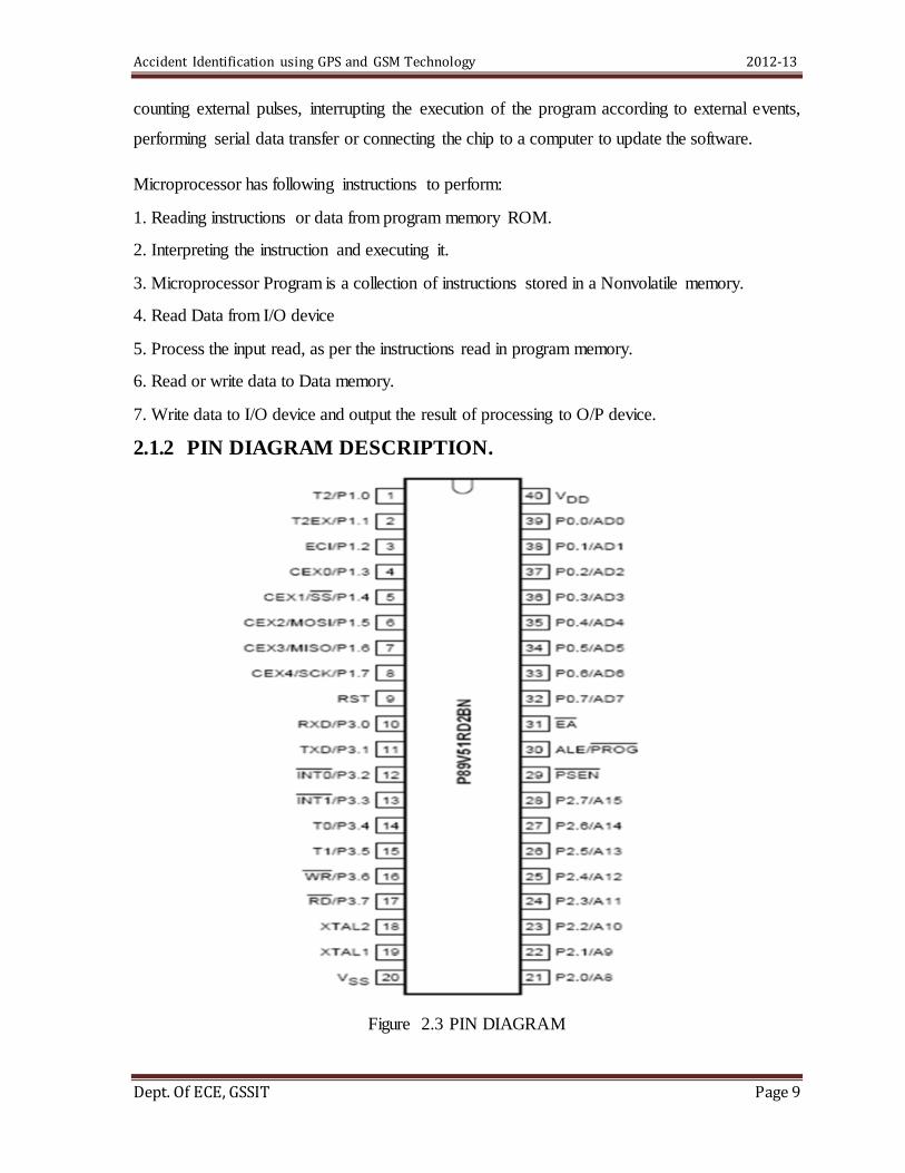
2.1.2 PIN DIAGRAM DESCRIPTION.
Figure 2.3 PIN DIAGRAM

Accident Identification using GPS and GSM Technology 2012-13
Dept. Of ECE, GSSIT Page 10
2.1.3 PIN DESCRIPTION
Pin Description:
Port 0
Port 0 is an 8-bit open drain bidirectional I/O port. As an output port, each pin can
sink eight TTL inputs. When 1s are written to port 0 pins, the pins can be used as
high impedance inputs. Port 0 can also be configured to be the multiplexed low order
address/data bus during accesses to external program and data memory. In this mode, P0 has
internal pull-ups. Port 0 also receives the code bytes during Flash programming and outputs
the code bytes during program verification. External pull-ups are required during program
verification.
Port 1
Port 1 is an 8-bit bidirectional I/O port with internal pull-ups. The Port 1 output
buffers can sink/source four TTL inputs. When 1s are written to Port 1 pins, they are
pulled high by the internal pull-ups and can be used as inputs. As inputs, Port 1 pins that
are externally being pulled low will source current (IIL) because of the internal pull-ups.
In addition, P1.0 and P1.1 can be configured to be the timer/counter 2 external count
input (P1.0/T2) and the timer/counter 2 trigger input (P1.1/T2EX), respectively, as
shown in the following table. Port 1 also receives the low-order address bytes during
Flash programming and verification.
PORT 2
Port 2 is an 8-bit bidirectional I/O port with internal pull-ups.The Port 2 output
buffers can sink/source four TTL inputs. When 1s are written to Port 2 pins, they are
pulled high by the internal pull-ups and can be used as inputs. As inputs, Port 2 pins that
are externally being pulled low will source current (IIL) because of the internal pull-ups.
Port 2 emits the high-order address byte during fetches from external program memory
and during accesses to external data memory that uses 16-bit addresses (MOVX @
DPTR). In this application, Port 2 uses strong internal pull-ups when emitting 1s. During
accesses to external data memory that uses 8-bit addresses (MOVX @ RI), Port 2 emits

Accident Identification using GPS and GSM Technology 2012-13
Dept. Of ECE, GSSIT Page 11
the contents of the P2 Special Function Register. Port 2 also receives the high-order
address bits and some control signals during Flash programming and verification.
PORT 3
Port 3 is an 8-bit bidirectional I/O port with internal pull-ups .The Port 3 output
buffers can sink/source four TTL inputs. When 1s are written to Port 3 pins, they are
pulled high by the internal pull-ups and can be used as inputs. As inputs, Port 3 pins that
are externally being pulled low will source current (IIL) because of the pull-ups. Port 3
also serves the functions of various special features of the AT89S52, as shown in the
following table. Port 3 also receives some control signals for Flash programming and
verification.
Table 2.1 Port 3 pin and it‟s functions
RST
Reset input. A high on this pin for two machine cycles while the oscillator is
running resets the device. This pin drives High for 96 oscillator periods after the
Watchdog times out. ALE/PROG Address Latch Enable (ALE) is an output pulse for
latching the low byte of the address during accesses to external memory. This pin is also
the program pulse input (PROG) during Flash programming. In normal operation, ALE is
emitted at a constant rate of 1/6 the oscillator frequency and may be used for external
timing or clocking purposes. Note, however, that one ALE pulse is skipped during each
access to external data memory. If desired, ALE operation can be disabled by setting bit 0
Accident Identification using GPS and GSM Technology 2012-13
Dept. Of ECE, GSSIT Page 12
of SFR location 8EH. With the bit set, ALE is active only during a MOVX or MOVC
instruction. Otherwise, the pin is weakly pulled high. Setting the ALE-disable bit has no
effect if the microcontroller is in external execution mode.
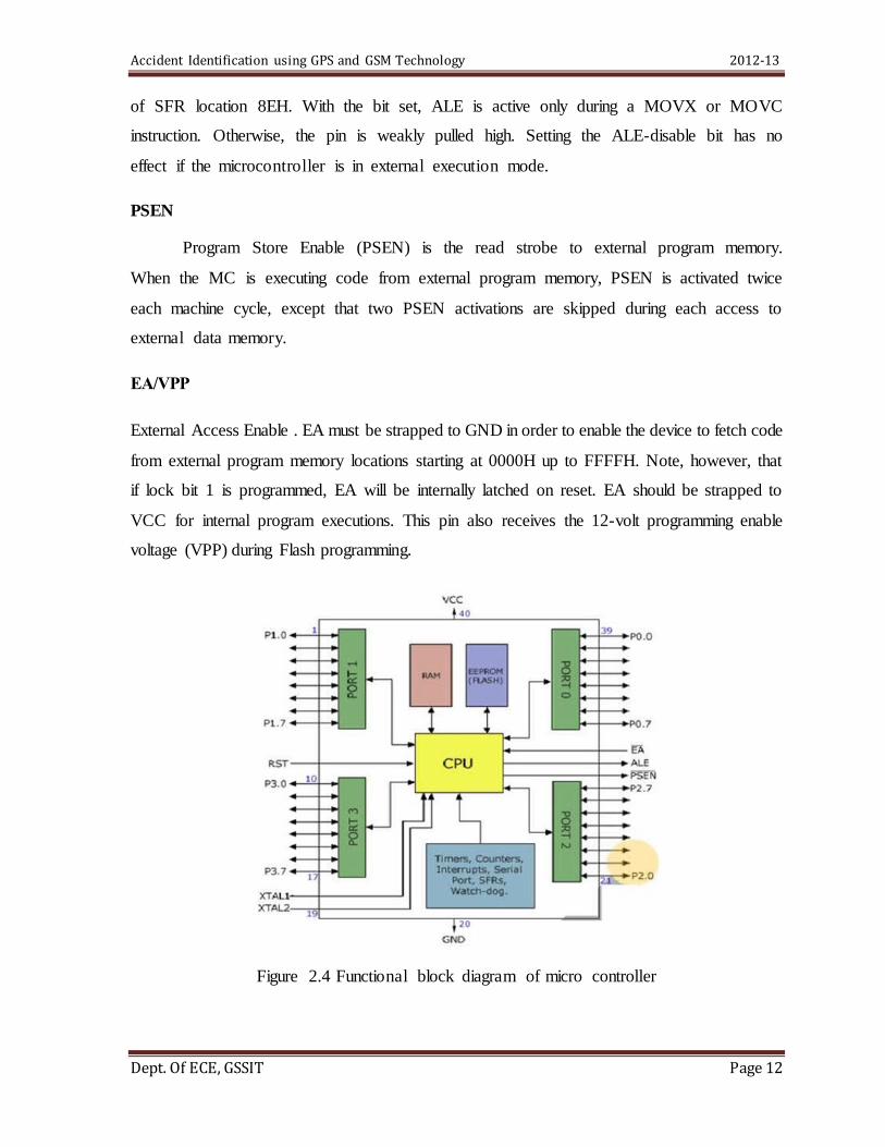
PSEN
Program Store Enable (PSEN) is the read strobe to external program memory.
When the MC is executing code from external program memory, PSEN is activated twice
each machine cycle, except that two PSEN activations are skipped during each access to
external data memory.
EA/VPP
External Access Enable . EA must be strapped to GND in order to enable the device to fetch code
from external program memory locations starting at 0000H up to FFFFH. Note, however, that
if lock bit 1 is programmed, EA will be internally latched on reset. EA should be strapped to
VCC for internal program executions. This pin also receives the 12-volt programming enable
voltage (VPP) during Flash programming.
Figure 2.4 Functional block diagram of micro controller

Accident Identification using GPS and GSM Technology 2012-13
Dept. Of ECE, GSSIT Page 13
2.2 The 8052 Oscillator and Clock:
The heart of the 8051 circuitry that generates the clock pulses by which all the internal all
internal operations are synchronized. Pins XTAL1 And XTAL2 is provided for
connecting a resonant network to form an oscillator. Typically a quartz crystal and
capacitors are employed. The crystal frequency is the basic internal clock frequency of
the microcontroller. The manufacturers make 8051 designs that run at specific minimum
and maximum frequencies typically 1 to 16 MHz.
Fig-2.5 Oscillator and timing circuit

Accident Identification using GPS and GSM Technology 2012-13
Dept. Of ECE, GSSIT Page 14
2.3 MEMORIES
Types of memory: The 8052 have three general types of memory. They are on-chip
memory, external Code memory and external Ram. On-Chip memory refers to physically
existing memory on the micro controller itself. External code memory is the code
memory that resides off chip. This is often in the form of an external EPROM. External
RAM is the Ram that resides off chip. This often is in the form of standard static RAM or
flash RAM.
a) Code memory
Code memory is the memory that holds the actual 8052 programs that is to be run. This
memory is limited to 64K. Code memory may be found on-chip or off-chip. It is possible
to have 8K of code memory on-chip and 60K off chip memory simultaneously. If only
off-chip memory is available then there can be 64K of off chip ROM. This is controlled
by pin provided as EA
b) Internal RAM
The 8052 have a bank of 256 bytes of internal RAM. The internal RAM is found on-chip.
So it is the fastest Ram available. And also it is most flexible in terms of reading and
writing. Internal Ram is volatile, so when 8051 is reset, this memory is cleared. 256 bytes
of internal memory are subdivided. The first 32 bytes are divided into 4 register banks.
Each bank contains 8 registers. Internal RAM also contains 256 bits, which are addressed
from 20h to 2Fh. These bits are bit addressed i.e. each individual bit of a byte can be
addressed by the user. They are numbered 00h to FFh. The user may make use of these
variables with commands such as SETB and CLR. Special Function registered memory:
Special function registers are the areas of memory that control specific functionality of
the 8052 micro controller.
a) Accumulator (0E0h)
As its name suggests, it is used to accumulate the results of large no of instructions. It can
hold 8 bit values.

Accident Identification using GPS and GSM Technology 2012-13
Dept. Of ECE, GSSIT Page 15
b) B registers (0F0h)
The B register is very similar to accumulator. It may hold 8-bit value. The b register is
only used by MUL AB and DIV AB instructions. In MUL AB the higher byte of the
product gets stored in B register. In div AB the quotient gets stored in B with the
remainder in A.
1. Stack pointer (81h)
The stack pointer holds 8-bit value. This is used to indicate where the next value to be
removed from the stack should be taken from. When a value is to be pushed onto the
stack, the 8052 first store the value of SP and then store the value at the resulting memory
location. When a value is to be popped from the stack, the 8052 returns the value from the
memory location indicated by SP and then decrements the value of SP.
d) Data pointer
The SFRs DPL and DPH work together work together to represent a 16-bit value called
the data pointer. The data pointer is used in operations regarding external RAM and some
instructions code memory. It is a 16-bit SFR and also an addressable SFR.
e) Program counter
The program counter is a 16 bit register, which contains the 2 byte address, which tells
the 8052 where the next instruction to execute to be found in memory. When the 8052 is
initialized PC starts at 0000h. And is incremented each time an instruction is executes. It
is not addressable SFR.
f) PCON (power control, 87h)
The power control SFR is used to control the 8051‟s power control modes. Certain
operation modes of the 8051 allow the 8051 to go into a type of “sleep mode” which
consumes much lee power.

Accident Identification using GPS and GSM Technology 2012-13
Dept. Of ECE, GSSIT Page 16
g) TCON (timer control, 88h)
The timer control SFR is used to configure and modify the way in which the 8051‟s two
timers operate. This SFR controls whether each of the two timers is running or stopped
and contains a flag to indicate that each timer has overflowed. Additionally, some non-
timer related bits are located in TCON SFR. These bits are used to configure the way in
which the external interrupt flags are activated, which are set when an external interrupt
occurs.
h) TMOD (Timer Mode, 89h)
The timer mode SFR is used to configure the mode of operation of each of the two
timers. Using this SFR your program may configure each timer to be a 16-bit timer, or 13
bit timer, 8-bit auto reload timer, or two separate timers. Additionally you may configure
the timers to only count when an external pin is activated or to count “events” that are
indicated on an external pin.
i) TO (Timer 0 low/high, address 8A/8C h)
These two SFRs taken together represent timer 0. Their exact behavior depends on how
the timer is configured in the TMOD SFR; however, these timers always count up. What
is configurable is how and when they increment in value.
j) T1 (Timer 1 Low/High, address 8B/ 8D h)
These two SFRs, taken together, represent timer 1. Their exact behavior depends on how
the timer is configured in the TMOD SFR; however, these timers always count up..
Accident Identification using GPS and GSM Technology 2012-13
Dept. Of ECE, GSSIT Page 17
k) P0 (Port 0, address 90h, bit addressable)
This is port 0 latch. Each bit of this SFR corresponds to one of the pins on a micro
controller. Any data to be outputted to port 0 is first written on P0 register. For e.g., bit 0
of port 0 is pin P0.0, bit 7 is pin p0.7. Writing a value of 1 to a bit of this SFR will send a
high level on the corresponding I/O pin whereas a value of 0 will bring it to low level.
l) P1 (port 1, address 90h, bit addressable)
This is port latch1. Each bit of this SFR corresponds to one of the pins on a micro
controller. Any data to be outputted to port 0 is first written on P0 register. For e.g., bit 0
of port 0 is pin P1.0, bit 7 is pin P1.7. Writing a value of 1 to a bit of this SFR will send a
high level on the corresponding I/O pin whereas a value of 0 will bring it to low level
m) P2 (port 2, address 0A0h, bit addressable):
This is a port latch2. Each bit of this SFR corresponds to one of the pins on a micro
controller. Any data to be outputted to port 0 is first written on P0 register. For e.g., bit 0
of port 0 is pin P2.0, bit 7 is pin P2.7. Writing a value of 1 to a bit of this SFR will send a
high level on the corresponding I/O pin whereas a value of 0 will bring it to low level.
n) P3 (port 3, address B0h, bit addressable) :
This is a port latch3. Each bit of this SFR corresponds to one of the pins on a micro
controller. Any data to be outputted to port 0 is first written on P0 register. For e.g., bit 0
of port 0 is pin P3.0, bit 7 is pin P3.7. Writing a value of 1 to a bit of this SFR will send a
high level on the corresponding I/O pin whereas a value of 0 will bring it to low level.
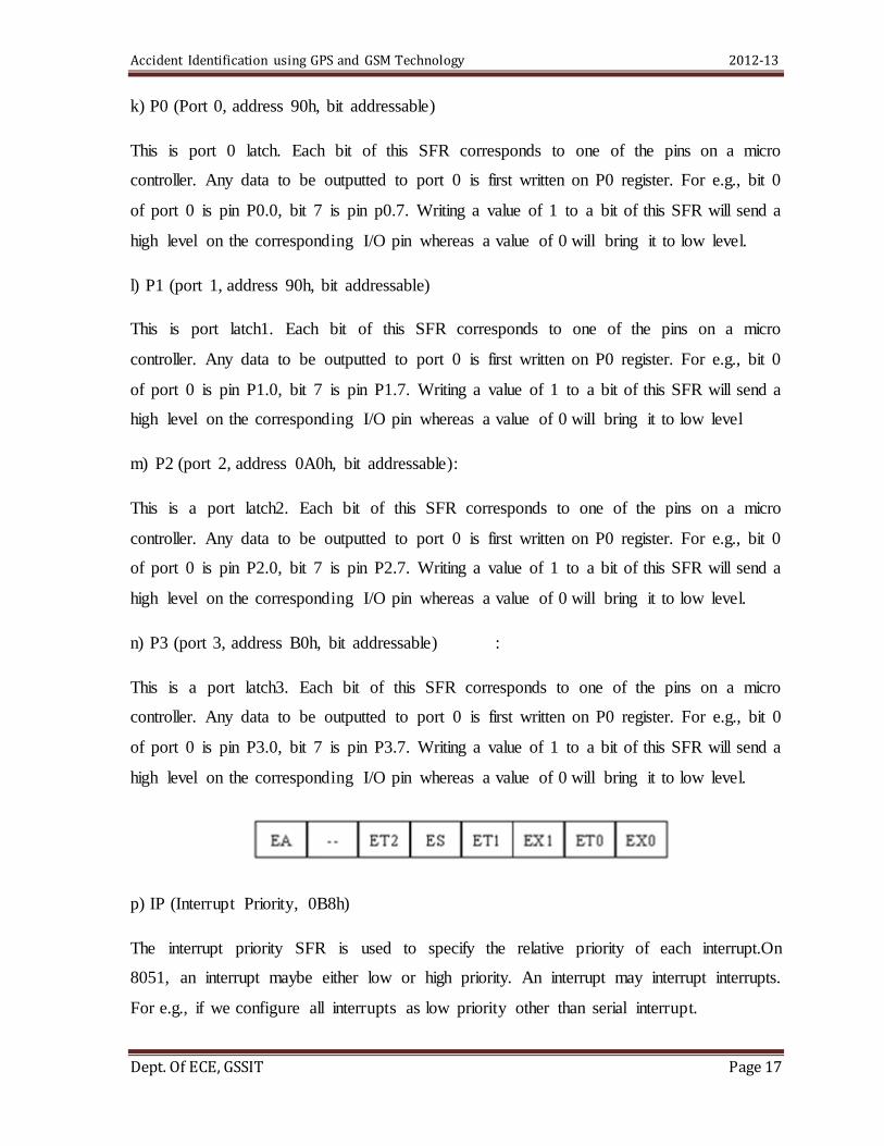
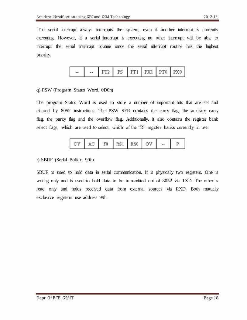
p) IP (Interrupt Priority, 0B8h)
The interrupt priority SFR is used to specify the relative priority of each interrupt.On
8051, an interrupt maybe either low or high priority. An interrupt may interrupt interrupts.
For e.g., if we configure all interrupts as low priority other than serial interrupt.
Accident Identification using GPS and GSM Technology 2012-13
Dept. Of ECE, GSSIT Page 18
The serial interrupt always interrupts the system, even if another interrupt is currently
executing. However, if a serial interrupt is executing no other interrupt will be able to
interrupt the serial interrupt routine since the serial interrupt routine has the highest
priority.
q) PSW (Program Status Word, 0D0h)
The program Status Word is used to store a number of important bits that are set and
cleared by 8052 instructions. The PSW SFR contains the carry flag, the auxiliary carry
flag, the parity flag and the overflow flag. Additionally, it also contains the register bank
select flags, which are used to select, which of the “R” register banks currently in use.
r) SBUF (Serial Buffer, 99h)
SBUF is used to hold data in serial communication. It is physically two registers. One is
writing only and is used to hold data to be transmitted out of 8052 via TXD. The other is
read only and holds received data from external sources via RXD. Both mutually
exclusive registers use address 99h.

Accident Identification using GPS and GSM Technology 2012-13
Dept. Of ECE, GSSIT Page 19
CHAPTER 3
POWER SUPPLY
All digital circuits require regulated power supply. In this article we are going to learn
how to get a regulated positive supply from the mains supply.
Figure 3.1 Basic block diagram of a fixed regulated power supply
3.1 TRANSFORMER
Figure 3.2 Transformer and it‟s type
A transformer consists of two coils also called as “WINDINGS” namely
PRIMARY & SECONDARY. They are linked together through inductively coupled
electrical conductors also called as CORE. A changing current in the primary causes a
Accident Identification using GPS and GSM Technology 2012-13
Dept. Of ECE, GSSIT Page 20
change in the Magnetic Field in the core & this in turn induces an alternating voltage in
the secondary coil. If load is applied to the secondary then an alternating current will flow
through the load. If we consider an ideal condition then all the energy from the primary
circuit will be transferred to the secondary circuit through the magnetic field. The
secondary voltage of the transformer depends on the number of turns in the Primary as
well as in the secondary.
3.2 Rectifier
A rectifier is a device that converts an AC signal into DC signal. For rectification
purpose we use a diode, a diode is a device that allows current to pass only in one
direction i.e. when the anode of the diode is positive with respect to the cathode also
called as forward biased condition & blocks current in the reversed biased condition.
Rectifier can be classified as follows:
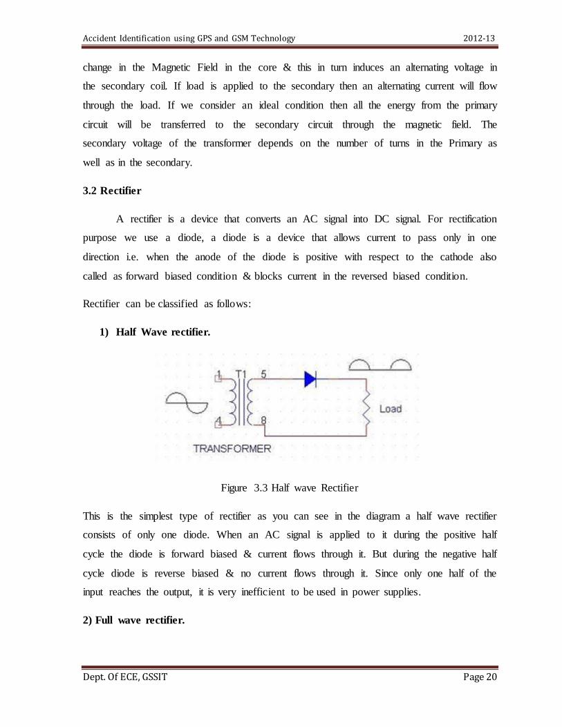
1) Half Wave rectifier.
Figure 3.3 Half wave Rectifier
This is the simplest type of rectifier as you can see in the diagram a half wave rectifier
consists of only one diode. When an AC signal is applied to it during the positive half
cycle the diode is forward biased & current flows through it. But during the negative half
cycle diode is reverse biased & no current flows through it. Since only one half of the
input reaches the output, it is very inefficient to be used in power supplies.
2) Full wave rectifier.

Accident Identification using GPS and GSM Technology 2012-13
Dept. Of ECE, GSSIT Page 21
Figure 3.4 Full Wave Rectifier
Half wave rectifier is quite simple but it is very inefficient, for greater efficiency
we would like to use both the half cycles of the AC signal. This can be achieved by using
a center tapped transformer i.e. we would have to double the size of secondary winding &
provide connection to the center. So during the positive half cycle diode D1 conducts &
D2 is in reverse biased condition. During the negative half cycle diode D2 conducts & D1
is reverse biased. Thus we get both the half cycles across the load. One of the
disadvantages of Full Wave Rectifier design is the necessity of using a center tapped
transformer, thus increasing the size & cost of the circuit. This can be avoided by using
the Full Wave Bridge Rectifier.
3) Bridge Rectifier.
Figure 3.5 Bridge Rectifier
As the name suggests it converts the full wave i.e. both the positive & the negative half
cycle into DC thus it is much more efficient than Half Wave Rectifier & that too without
using a center tapped transformer thus much more cost effective than Full Wave Rectifier.
Accident Identification using GPS and GSM Technology 2012-13
Dept. Of ECE, GSSIT Page 22
Full Bridge Wave Rectifier consists of four diodes namely D1, D2, D3 and D4. During
the positive half cycle diodes D1 & D4 conduct whereas in the negative half cycle diodes
D2 & D3 conduct thus the diodes keep switching the transformer connections so we get
positive half cycles in the output.
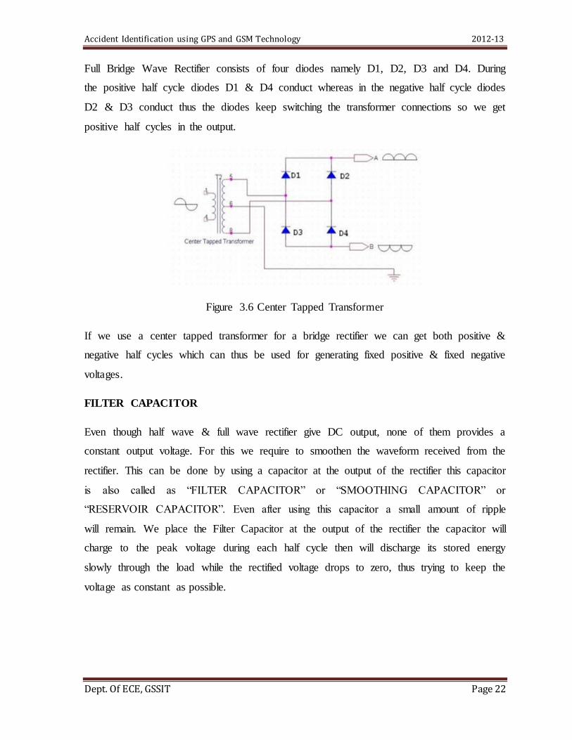
Figure 3.6 Center Tapped Transformer
If we use a center tapped transformer for a bridge rectifier we can get both positive &
negative half cycles which can thus be used for generating fixed positive & fixed negative
voltages.
FILTER CAPACITOR
Even though half wave & full wave rectifier give DC output, none of them provides a
constant output voltage. For this we require to smoothen the waveform received from the
rectifier. This can be done by using a capacitor at the output of the rectifier this capacitor
is also called as “FILTER CAPACITOR” or “SMOOTHING CAPACITOR” or
“RESERVOIR CAPACITOR”. Even after using this capacitor a small amount of ripple
will remain. We place the Filter Capacitor at the output of the rectifier the capacitor will
charge to the peak voltage during each half cycle then will discharge its stored energy
slowly through the load while the rectified voltage drops to zero, thus trying to keep the
voltage as constant as possible.

Accident Identification using GPS and GSM Technology 2012-13
Dept. Of ECE, GSSIT Page 23
Figure 3.7 variation in Voltage
Figure 3.8 Filter Capacitor Varying Voltage Characteristics
If we go on increasing the value of the filter capacitor then the Ripple will decrease. But
then the costing will increase. The value of the Filter capacitor depends on the current
consumed by the circuit, the frequency of the waveform & the accepted ripple.
3.3 VOLTAGE REGULATOR
A Voltage regulator is a device which converts varying input voltage into a constant
regulated output voltage. Voltage regulator can be of two types
1) Linear Voltage Regulator Also called as Resistive Voltage regulator because they
dissipate the excessive voltage resistively as heat.
2) Switching Regulators. They regulate the output voltage by switching the Current
ON/OFF very rapidly. Since their output is either ON or OFF it dissipates very low power
thus achieving higher efficiency as compared to linear voltage regulators. But they are
more complex & generate high noise due to their switching action. For low level of
output power switching regulators tend to be costly but for higher output wattage they are
much cheaper than linear regulators.
The most commonly available Linear Positive Voltage Regulators are the 78XX series
where the XX indicates the output voltage. And 79XX series is for Negative Voltage
Regulators.

Accident Identification using GPS and GSM Technology 2012-13
Dept. Of ECE, GSSIT Page 24
Figure 3.9 78xx series Regulator
After filtering the rectifier output the signal is given to a voltage regulator. The maximum
input voltage that can be applied at the input is 35V.Normally there is a 2-3 Volts drop
across the regulator so the input voltage should be at least 2-3 Volts higher than the
output voltage. If the input voltage gets below the Vmin of the regulator due to the ripple
voltage or due to any other reason the voltage regulator will not be able to produce the
correct regulated voltage.
Figure 3.10 7805 Regulator
(ii) IC 7805:
7805 is an integrated three-terminal positive fixed linear voltage regulator. It supports an
input voltage of 10 volts to 35 volts and output voltage of 5 volts. It has a current rating of
1 amp although lower current models are available. Its output voltage is fixed at 5.0V.
The 7805 also has a built-in current limiter as a safety feature. 7805 is manufactured by
many companies, including National Semiconductors and Fairchild Semiconductors.

Accident Identification using GPS and GSM Technology 2012-13
Dept. Of ECE, GSSIT Page 25
The 7805 will automatically reduce output current if it gets too hot. The last two digits
represent the voltage; for instance, the 7812 is a 12-volt regulator. The 78xx series of
regulators is designed to work in complement with the 79xx series of negative voltage
regulators in systems that provide both positive and negative regulated voltages, since the
78xx series can't regulate negative voltages in such a system.
The 7805 & 78 is one of the most common and well-known of the 78xx series regulators,
as it's small component count and medium-power regulated 5V make it useful for
powering TTL devices.
Specifications IC7805
Vin 5v
Vin –Vout 5v-20v
Operation Ambient Temp 0 - 125°C
Output Imax 1A
Table 3.1 Regulator Specifications
Accident Identification using GPS and GSM Technology 2012-13
Dept. Of ECE, GSSIT Page 26
CHAPTER 4
GSM MODEM
GSM (Global System for Mobile communications) is an open, digital cellular technology
used for transmitting mobile voice and data services.
GSM supports voice calls and data transfer speeds of up to 9.6 kbit/s, together with the
transmission of SMS (Short Message Service).
GSM operates in the 900MHz and 1.8GHz bands in Europe and the 1.9GHz and 850MHz
bands in the US. The 850MHz band is also used for GSM and 3G in Australia, Canada
and many South American countries. By having harmonized spectrum across most of
the globe, GSM‟s international roaming capability allows users to access the same
services when travelling abroad as at home. This gives consumers seamless and same
number connectivity in more than 218 countries.
4.1 HISTORY
In 1980‟s the analog cellular telephone systems were growing rapidly all throughout
Europe, France and Germany. Each country defined its own protocols and frequencies to
work on. For example UK used the Total Access Communication System (TACS), USA
used the AMPS technology and Germany used the C-netz technology. None of these
systems were interoperable and also they were analog in nature.
In 1982 the Conference of European Posts and Telegraphs (CEPT) formed a study group
called the GROUPE SPECIAL MOBILE (GSM) The main area this focused on was to
get the cellular system working throughout the world, and ISDN compatibility with the
ability to incorporate any future enhancements. In 1989 the GSM transferred the work to
the European Telecommunications Standards Institute (ETSI.) the ETS defined all the
standards used in GSM.

Accident Identification using GPS and GSM Technology 2012-13
Dept. Of ECE, GSSIT Page 27
4.2 BASICS OF WORKING AND SPECIFICATIONS OF GSM
The GSM architecture is nothing but a network of computers. The system has to partition
available frequency and assign only that part of the frequency spectrum to any base
transreceiver station and also has to reuse the scarce frequency as often as possible.
GSM uses TDMA and FDMA together. Graphically this can be shown below -
Figure 4.1 combination of FDMA and TDMA
Some of the technical specifications of GSM are listed below.

Accident Identification using GPS and GSM Technology 2012-13
Dept. Of ECE, GSSIT Page 28
GSM was originally defined for the 900 Mhz range but after some time even the 1800
Mhz range was used for cellular technology. The 1800 MHz range has its architecture and
specifications almost same to that of the 900 Mhz GSM technology but building the
Mobile exchanges is easier and the high frequency Synergy effects add to the advantages
of the 1800 Mhz range.
4.3 ARCITECTURE AND BUILDIGN BLOCKS.
GSM is mainly built on 3 building blocks.
GSM Radio Network - This is concerned with the signaling of the system. Hand-overs
occur in the radio network. Each BTS is allocated a set of frequency channels.
GSM Mobile switching Network - This network is concerned with the storage of data
required for routing and service provision.
GSM Operation and Maintenance - The task carried out by it include
Administration and commercial operation , Security management, Network
configuration, operation, performance management and maintenance tasks.
Figure 4.2: Structure of the Network

Accident Identification using GPS and GSM Technology 2012-13
Dept. Of ECE, GSSIT Page 29
Public Land Mobile Network(PLMN) The whole GSM system
Mobile System (MS) The actual cell phone that we use
Base Transceiver Station (BTS)
Provides connectivity between network and
mobile station via the Air- interface
BaseStationController(BSC)
Controls the whole subsystem.
Mobile Services Switching Center
The BSC is connected to the MSC. The MSC
routes the incoming and outgoing calls and assigns user cannels on the A- interface.
Home Location Register (HLR)
This register stores data of large no of users. It is like a database that manages data of all the
users. Every PLMN will have at least one HLR.
Visitor Location Resigter (VLR)
This contains part of data so that the HLR is not overloaded with inquiries. If a subscriber
moves out of VLR area the HLR requests removal of data related to that user from the
VLR.
Equipment Identity Register (EIR)
The IMEI no. is allocated by the
manufacturer
Table 4.1 The basic blocks of the whole GSM system
4.4 SIGNALLING SCHEMES USED -
Figure 4.3 Transmitter for the voice signal

Accident Identification using GPS and GSM Technology 2012-13
Dept. Of ECE, GSSIT Page 30
Figure 4.4 Receiver for the Voice signal
The voice signal is sampled at 8000 bits/sec and is quantized to get a 13 bit resolution
corresponding to a bit rate of 104 Kbits/sec. This signal is given to a speech coder (codec)
that compresses this speech into a source-coded speech signal of 260 bit blocks at a bit
rate of 13 Kbit/sec. The codec achieves a compression ratio of 1:8. The coder also has a
Voice activity detector (VAD) and comfort noise synthesizer. The VAD decides whether
the current speech frame contains speech or pause, this is turn is used to decide whether
to turn on or off the transmitter under the control of the Discontinuous Transmission
(DTX). This transmission takes advantage of the fact that during a phone conversation
both the parties rarely speak at the same time. Thus the DTX helps in reducing the power
consumption and prolonging battery life. The missing speech frames are replaced by
synthetic background noise generated by the comfort noise synthesize in a Silence
Descriptor (SID) frame. Suppose a loss off speech frame occurs due to noisy transmission
and it cannot be corrected by the channel coding protection mechanism then the decoder
flags such frames with a bad frame indicator (BFI) In such a case the speech frame is
discarded and using a technique called error concealment which calculates the next frame
based on the previous frame.

Accident Identification using GPS and GSM Technology 2012-13
Dept. Of ECE, GSSIT Page 31
4.5 AT Commands
Commands always start with AT (which means Attention) and finish with a <CR>
character. Information responses and result codes Responses start and end with
<CR><LF>, except for the ATV0 DCE response format) and the ATQ1 (result code
suppression) commands.
If command syntax is incorrect, an ERROR string is returned.
If command syntax is correct but with some incorrect parameters, the +CME ERROR:
<Err> or +CMS ERROR: <SmsErr> strings are returned with different error codes. If the
command line has been performed successfully, an OK string is returned. In some cases,
such as “AT+CPIN?” or (unsolicited) incoming events, the product does not Return the
OK string as a response.
Product Serial Number +CGSN Description
This command allows the user application to get the IMEI (International Mobile
Equipment Identity) of the product.
Syntax:
Command syntax: AT+CGSN
Command Possible responses
AT+CGSN 012345678901234
OK
Note : IMEI read from EEPROM
AT+CGSN +CME ERROR : 22
Note : IMEI not found in EEPROM
Table 4.2 syntax for getting IMEI
Repeat last command A/
Description: This command repeats the previous command. Only the A/ command itself
cannot be repeated.

Accident Identification using GPS and GSM Technology 2012-13
Dept. Of ECE, GSSIT Page 32
Syntax: Command syntax: A/
Command Possible Responses
A/
Note: Repeat last command
Table 4.3 Syntax for Repeat command
Signal Quality +CSQ
Description: This command determines the received signal strength indication (<rssi>)
and the channel bit error. Rate (<ber>) with or without a SIM card inserted.
Syntax: Command syntax: AT+CSQ
Command Possible Responses
AT+CSQ +CSQ : <rssi>,<ber>
OK
Note:<rssi> and <ber> as defined below
Table 4.4 Syntax for Received Signal Strength
Defined Values:
0: -113 dBm or less
1: -111 dBm
30: -109 to -53 dBm
31: -51dBm or greater
99: not known or not detectable
<ber>: 0…7: as RXQUAL values in the
table GSM 05.08 99: not known or not
detectable
New message indication +CNMI
Description: This command selects the procedure for message reception from the
network.
Accident Identification using GPS and GSM Technology 2012-13
Dept. Of ECE, GSSIT Page 33
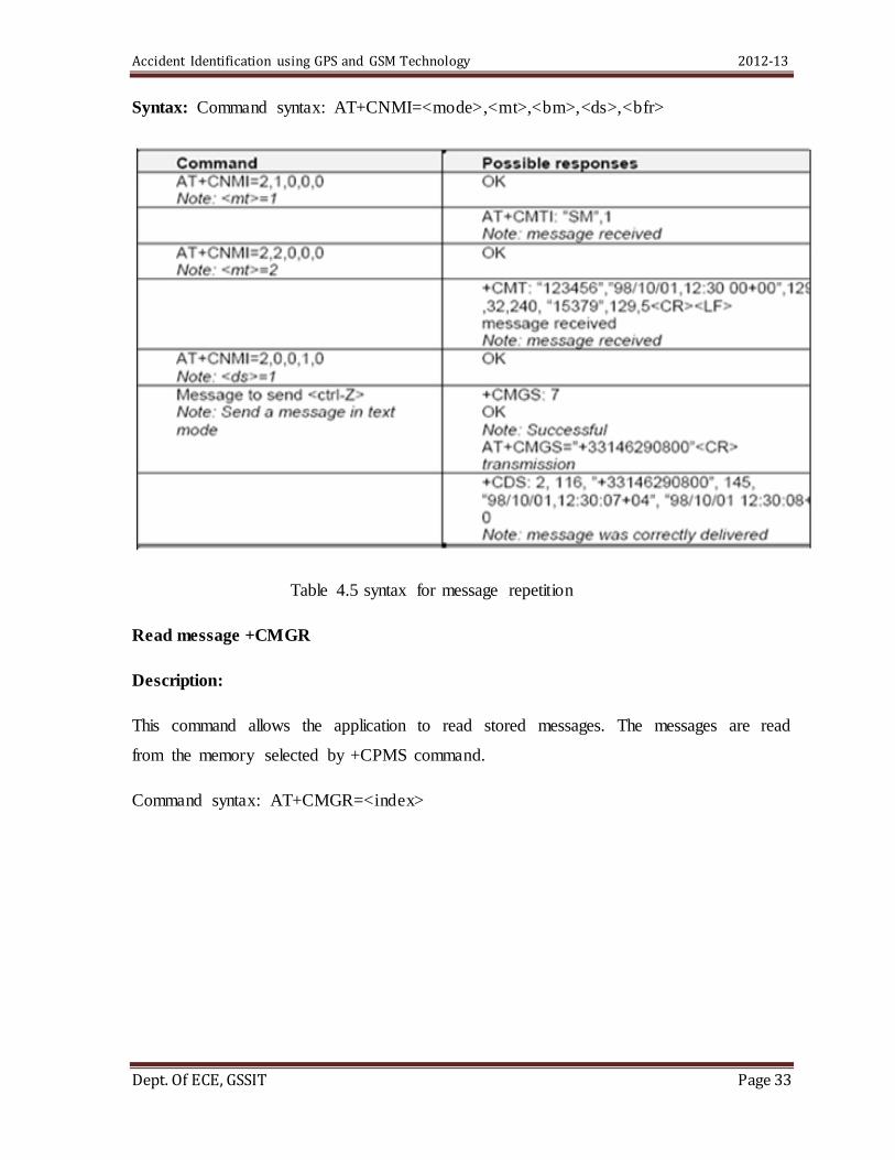
Syntax: Command syntax: AT+CNMI=<mode>,<mt>,<bm>,<ds>,<bfr>
Table 4.5 syntax for message repetition
Read message +CMGR
Description:
This command allows the application to read stored messages. The messages are read
from the memory selected by +CPMS command.
Command syntax: AT+CMGR=<index>

Accident Identification using GPS and GSM Technology 2012-13
Dept. Of ECE, GSSIT Page 34
Table 4.6 Syntax to Store messages
List message +CMGL
Description: This command allows the application to read stored messages, by indicating
the type of the Message to read. The messages are read from the memory selected by the
+CPMS command. Syntax: Command syntax: AT+CMGL=<stat> .
Table 4.7 Syntax to read stored messages
Defined values:

Accident Identification using GPS and GSM Technology 2012-13
Dept. Of ECE, GSSIT Page 35
<stat> possible values (status of messages in memory):
Table 4.8 syntax for status
Send message +CMGS
Description: The <address> field is the address of the terminal to which the message is
sent. To send the Message, simply type, <ctrl-Z> character (ASCII 26). The text can
contain all existing Characters except <ctrl-Z> and <ESC> (ASCII 27). This command
can be aborted using the <ESC> character when entering text. In PDU mode, only
hexadecimal characters are used („0‟…‟9‟,‟A‟…‟F‟).
Syntax:
Command syntax in text mode:
AT+CMGS=<da>[,<toda>]<CR>
text is entered <ctrl-Z / ESC >
Table 4.9 Syntax for text mode

Accident Identification using GPS and GSM Technology 2012-13
Dept. Of ECE, GSSIT Page 36
The message reference, <mr>, which is returned to the application, is allocated by
the product. This number begins with 0 and is incremented by one for each outgoing
message (successful and failure cases); it is cyclic on one byte (0 follows 255).
Note: This number is not a storage number. Outgoing messages are not stored.
Delete message +CMGD
Description:
This command deletes one or several messages from preferred message storage (“BM”
SMS
CB „RAM storage‟, “SM” SMSPP storage „SIM storage‟ or “SR” SMS Status-Report
storage).
Syntax:
Command syntax: AT+CMGD=<Index> [,<DelFalg>]
Table 4.10 syntax for deleting messages
Defines values
(1-20) when the preferred message storage is “BM”
Integer type values in the range of location numbers of SIM Message memory.

Accident Identification using GPS and GSM Technology 2012-13
Dept. Of ECE, GSSIT Page 37
When the preferred message storage is “SM” or “SR”.
<DelFlag>
0 Delete message at location <index>.
1 Delete All READ messages
2 Delete All READ and SENT messages
3 Delete All READ, SENT and UNSENT messages 4 Delete all messages.

Accident Identification using GPS and GSM Technology 2012-13
Dept. Of ECE, GSSIT Page 38
CHAPTER 5
GLOBAL POSITIONING SYSTEM
5.1 GPS Basics:
The Global Positioning System (GPS) is a space-based global navigation satellite
system (GNSS) that provides reliable location and time information in all weather and at all times
and anywhere on or near the Earth when and where there is an unobstructed line of sight to four
or more GPS satellites. It is maintained by the United States government and is freely accessible
by anyone with a GPS receiver. When people talk about "a GPS," they usually mean a GPS
receiver. The Global Positioning System (GPS) is actually a constellation of 27 Earth-orbiting
satellites (24 in operation and three extras in case one fails). The U.S. military developed and
implemented this satellite network as a military navigation system, but soon opened it up to
everybody else. Each of these 3,000- to 4,000-pound solar-powered satellites circles the globe at
about 12,000 miles (19,300 km), making two complete rotations every day. The orbits are
arranged so that at anytime, anywhere on Earth, there are at least four satellites "visible" in the
sky.
A GPS receiver calculates its position by precisely timing the signals sent by GPS
satellites high above the Earth. Each satellite continually transmits messages that include the time
the message was transmitted precise orbital information (the ephemeris) the general system
health and rough orbits of all GPS satellites (the almanac).
The receiver uses the messages it receives to determine the transit time of each message
and computes the distance to each satellite. These distances along with the satellites' locations are
used with the possible aid of trilateration, depending on which algorithm is used, to compute the
position of the receiver. This position is then displayed, perhaps with a moving map display or
latitude and longitude; elevation information may be included. Many GPS units show derived
information such as direction and speed, calculated from position changes.
5.2 GPS Principle:
The GPS satellites act as reference points from which receivers on the ground detect their

Accident Identification using GPS and GSM Technology 2012-13
Dept. Of ECE, GSSIT Page 39
position. The fundamental navigation principle is based on the measurement of pseudo ranges
between the user and four satellites. Ground stations precisely monitor the orbit of every satellite
and by measuring the travel time of the signals transmitted from the satellite four distances
between receiver and satellites will yield accurate position, direction and speed. Though three -
range measurements are sufficient, the fourth observation is essential for solving clock
synchronization error between receiver and satellite. Thus, the term ―pseudo ranges‖ is derived.
The secret of GPS measurement is due to the ability of measuring carrier phases to about 1/100
of a cycle equalling to 2 to 3 mm in linear distance. Moreover the high frequency L1 and L2
carrier signal can easily penetrate the ionosphere to reduce its effect. Dual frequency observations
are important for large station separation and for eliminating most of the error parameters.
5.3 GPS Receiver:
A GPS navigation device is any device that receives Global Positioning System (GPS)
signals for the purpose of determining the device's current location on Earth. GPS devices
provide latitude and longitude information, and some may also calculate altitude, although this is
not considered sufficiently accurate or continuously available enough (due to the possibility of
signal blockage and other factors) to rely on exclusively to pilot aircraft. GPS devices are used in
military, aviation, marine and consumer product applications.
The user segment is composed of hundreds of thousands of U.S. and allied military users
of the secure GPS Precise Positioning Service, and tens of millions of civil, commercial and
scientific users of the Standard Positioning Service.
GPS receivers are composed of an antenna, tuned to the frequencies transmitted by the
satellites, receiver-processors, and a highly stable clock (often a crystal oscillator). They may also
include a display for providing location and speed information to the user. A receiver is often
described by its number of channels: this signifies how many satellites it can monitor
simultaneously. Originally limited to four or five, this has progressively increased over the years
so that, as of 2007, receivers typically have between 12 and 20 channels. GPS receivers may
include an input for differential corrections, using the RTCM SC-104 format. This is typically in
the form of an RS-232 port at 4,800 bit/s speed. Data is actually sent at a much lower rate, which
limits the accuracy of the signal sent using RTCM. Receivers with internal DGPS receivers can
outperform those using external RTCM data. As of 2006, even low-cost units commonly include

Accident Identification using GPS and GSM Technology 2012-13
Dept. Of ECE, GSSIT Page 40
Wide Area Augmentation System (WAAS) receivers. Many GPS receivers can relay position
data to a PC or other device using the NMEA 0183 protocol.
5.4 Major Components of a GPS Receiver:
The main components of a GPS receiver are :
Antenna with pre-amplifier
RF section with signal identification and signal processing
Micro-processor for receiver control, data sampling and data processing
oscillator
Power supply
User interface, command and display panel
Memory, data storage.
5.5 Function Of GPS:
It is a "constellation" of twenty-four 20,000km high GPS satellites. The satellites are
distributed on 6 orbits, 4 per orbit. Every satellite makes a complete rotation of the Earth every 12
hours. Every satellite possesses an atomic clock, allowing a very precise measure of time. They
emit on two different frequencies: L1: 1575 MHz and L2: 1227 MHz. L2 being reserved for the
American Army. Every satellite thus sends ceaselessly a code of 1500 bits, containing numerous
data such as the time at which the code is to be sent, the position of the satellite, its state, the
position of the other satellites... This data allows the receiver to calculate its position.
Each GPS satellite transmits radio signals that enable the GPS receivers to calculate
where its (or your vehicles) location on the Earth and convert the calculations into geodetic
latitude, longitude and velocity. A receiver needs signals from at least three GPS satellites to
pinpoint your vehicle„s position.
GPS Receivers commonly used in most Vehicle tracking systems can only receive data
from GPS Satellites. They cannot communicate back with GPS or any other satellite.
A system based on GPS can only calculate its location but cannot send it to central
control room. In order to do this they normally use GSM-GPRS Cellular networks connectivity
using additional GSM modem/module. Two levels of navigation and positioning are offered by
the Global Positioning System: The Standard Positioning Service (SPS). and the Precise
Positioning Service (PPS). The Precise Positioning Service is a highly accurate positioning,

Accident Identification using GPS and GSM Technology 2012-13
Dept. Of ECE, GSSIT Page 41
velocity and timing service that is designed primarily for the military and other authorized
users, although under certain conditions can be used by civilians who have specialized
equipment. The Standard Positioning Service offers a base-line accuracy that is much lower than
the PPS, but is available to all users with even the most inexpensive receivers. As we will see,
there are various techniques available that substantially increase the SPS accuracy, even well
beyond that which is offered by the PPS.
5.6 RECEIVER OUTPUT:
Typically receivers provide two different formats.
1. NMEA (Nation Marine Electronics Association) ASCII Format
Defines a set of standard messages.
2. Proprietary Format
Typically Binary
No limit on information transmitted
Receiver output is related to position, velocity and time. The output in the following
Position:
Latitude: degrees: minutes: seconds
Longitude: degrees: minutes: seconds
Altitude m
Velocity:
Speed knots
Heading degrees
Time (UTC):
Date dd/mm/yy
Time hh/mm/ss.sss
GPS receiver gives the latitude, longitude, date, time, speed of
the satellite, no of satellites on view etc…

Accident Identification using GPS and GSM Technology 2012-13
Dept. Of ECE, GSSIT Page 42
The National Marine Electronics Association (NMEA) has developed a specification that
defines the interface between various pieces of marine electronic equipment. The standard
permits marine electronics to send information to computers and to other marine equipment. A
full copy of this standard is available for purchase at their web site. None of the information on
this site comes from this standard and I do not have a copy. Anyone attempting to design
anything to this standard should obtain an official copy.
5.7 RECEIVER FEATURES:
12 parallel channel L1 Band SPS GPS.
Very good acquisition and good tracking sensitivity.
Antenna open short detection/protection
Tracking sensitivity:-154dB-m
Acquisition sensitivity -148dB-m
5v and 3.3volt option available
Most computer programs that provide real time position information understand and
expect data to be in NMEA format. This data includes the complete PVT (position, velocity,
time) solution computed by the GPS receiver. The idea of NMEA is to send a line of data called a
sentence that is totally self-contained and independent from other sentences. There are standard
sentences for each device category and there is also the ability to define proprietary sentences for
use by the individual company. All of the standard sentences have a two-letter prefix that defines
the device that uses that sentence type. (For GPS receivers the prefix is GP.) This is followed by
a three-letter sequence that defines the sentence contents. In addition NMEA permits hardware
manufactures to define their own proprietary sentences for whatever purpose they see fit. All
proprietary sentences begin with the letter P and are followed with 3 letters that identifies the
manufacturer controlling that sentence. For example a Garmin sentence would start with PGRM
and Magellan would begin with PMGN.
Each sentence begins with a '$' and ends with a carriage return/line feed sequence and can
be no longer than 80 characters of visible text (plus the line terminators). The data is contained
within this single line with data items separated by commas. The data itself is just ASCII text and
may extend over multiple sentences in certain specialized instances but is normally fully
contained in one variable length sentence. The data may vary in the amount of precision
Accident Identification using GPS and GSM Technology 2012-13
Dept. Of ECE, GSSIT Page 43
contained in the message. For example time might be indicated to decimal parts of a second or
location may be show with 3 or even 4 digits after the decimal point. Programs that read the data
should only use the commas to determine the field boundaries and not depend on column
positions. There is a provision for a checksum at the end of each sentence, which may or may not
be checked by the unit that reads the data. The checksum field consists of a '*' and two hex digits
representing an 8 bit exclusive OR of all characters between, but not including, the '$' and '*'. A
checksum is required on some sentences.
There have been several changes to the standard but for GPS use the only ones that are
likely to be encountered are 1.5 and 2.0 through 2.3. These just specify some different sentence
configurations which may be peculiar to the needs of a particular device thus the GPS may need
to be changed to match the devices being interfaced to. Some GPS's provide the ability configure
a custom set the sentences while other may offer a set of fixed choices. Many GPS receivers
simply output a fixed set of sentences that cannot be changed by the user. The current version of
the standard is 3.01. I have no specific information on this version, but I am not aware of any
GPS products that require conformance to this version.
5.8 Hardware Connection:
The hardware interface for GPS units is designed to meet the NMEA requirements. They
are also compatible with most computer serial ports using RS232 protocols, however strictly
speaking the NMEA standard is not RS232. They recommend conformance to EIA-422. The
interface speed can be adjusted on some models but the NMEA standard is 4800 b/s (bit per
second rate) with 8 bits of data, no parity, and one stop bit. All units that support NMEA should
support this speed. Note that, at a b/s rate of 4800, you can easily send enough data to more than
fill a full second of time. For this reason some units only send updates every two seconds or may
send some data every second while reserving other data to be sent less often. In addition some
units may send data a couple of seconds old while other units may send data that is collected
within the second it is sent. Generally time is sent in some field within each second so it is pretty
easy to figure out what a particular GPS is doing. Some sentences may be sent only during a
particular action of the receiver such as while following a route while other receivers may always
send the sentence and just null out the values. Other difference will be noted in the specific data
descriptions defined later in the text. At 4800 b/s you can only send 480 characters in one second.
Since an NMEA sentence can be as long as 82 characters you can be limited to less than 6

Accident Identification using GPS and GSM Technology 2012-13
Dept. Of ECE, GSSIT Page 44
different sentences. The actual limit is determined by the specific sentences used, but this shows
that it is easy to overrun the capabilities if you want rapid sentence response. NMEA is designed
to run as a process in the background spitting out sentences which are then captured as needed by
the using program. Some programs cannot do this and these programs will sample the data
stream, then use the data for screen display, and then sample the data again. Depending on the
time needed to use the data there can easily be a lag of 4 seconds in the responsiveness to
changed data. This may be fine in some applications but totally unacceptable in others. For
example a car traveling at 60 mph will travel 88 feet in one second. Several second delays could
make the entire system seem unresponsive and could cause you to miss
your turn.
The NMEA standard has been around for many years (1983) and has undergone several
revisions. The protocol has changed and the number and types of sentences may be different
depending on the revision. Most GPS receivers understand the standard, which is called: 0183
version 2. This standard dictates a transfer rate of 4800 b/s. Some receivers also understand older
standards. The oldest standard was 0180 followed by 0182, which transferred data at 1200 b/s.
Some receivers also understand an earlier version of 0183 called version 1.5. Some Garmin units
and other brands can be set to 9600 for NMEA output or even higher but this is only
recommended if you have determined that 4800 works ok and then you can try to set it faster.
Setting it to run as fast as you can may improve the responsiveness of the program.

Accident Identification using GPS and GSM Technology 2012-13
Dept. Of ECE, GSSIT Page 45
CHAPTER 6
ACCELEROMETER SENSOR
Accelerometers are sensors or transducers that measure acceleration.
Accelerometers generally measure acceleration forces applied to a body by being
mounted directly onto a surface of the accelerated body. Accelerometers are useful in
detecting motion in objects.
An accelerometer measures force exerted by a body as a result of a change in
the velocity of the body. A moving body possesses an inertia which tends to resist
change in velocity. It is this resistance to change in velocity that is the source of the
force exerted by the moving body. This force is directly proportional to the acceleration
component in the direction of movement when the moving body is accelerated. The
motion is detected in a sensitive portion of the accelerometer. This motion is indicative
of motion in the larger object or application in which the accelerometer is mounted.
Thus, a sensitive accelerometer can quickly detect motion in the application.
6.1 ADXL330:
3 Axis Acceleration Sensor Board based on ADXL330 from Analog devices. It is a first
generation 3 axis acceleration sensor. User could get acceleration value of X, Y, and Z axis. And
it is widely used in shock, slope, and moving detection. Output sensitivity could be select by
simply set voltage level on few pins. The output of MMA7260Q is analog mode, so you need a
A/D converter to read the acceleration value.
6.2FEATURES OF ADXL330 :
3-axis sensing Small, low profile package 4 mm × 4 mm × 1.45 mm
LFCSP Low power : 350 mA (typical) Single-Supply operation: 1.8 V to 3.6 V
10,000 g shock survival
Excellent temperature stability
BW adjustment with a single capacitor per axis
RoHS/WEEE lead-free compliant

Accident Identification using GPS and GSM Technology 2012-13
Dept. Of ECE, GSSIT Page 46
6.3 Functional Block Diagram:
Figure 6.1 Functional Block Diagram of ADXL330
Pin Configuration:
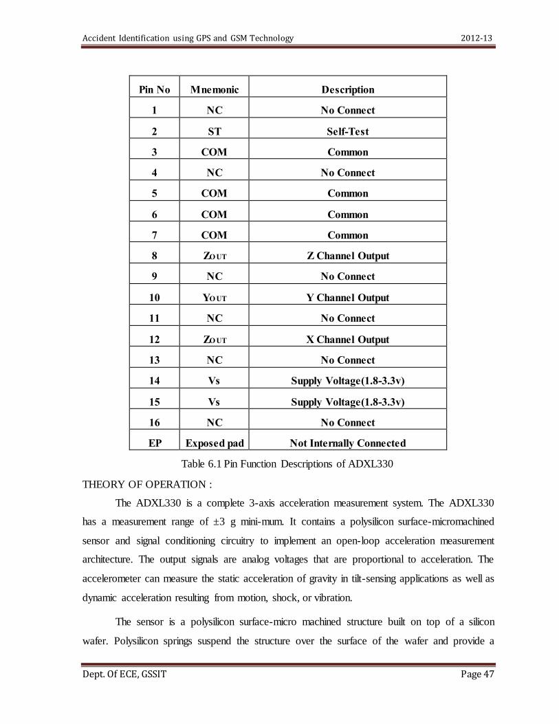
Figure 6.2 Pin Configuration of ADXL330
Accident Identification using GPS and GSM Technology 2012-13
Dept. Of ECE, GSSIT Page 47
Pin No Mnemonic Description
1 NC No Connect
2 ST Self-Test
3 COM Common
4 NC No Connect
5 COM Common
6 COM Common
7 COM Common
8 ZO UT Z Channel Output
9 NC No Connect
10 YO UT Y Channel Output
11 NC No Connect
12 ZO UT X Channel Output
13 NC No Connect
14 Vs Supply Voltage(1.8-3.3v)
15 Vs Supply Voltage(1.8-3.3v)
16 NC No Connect
EP Exposed pad Not Internally Connected
Table 6.1 Pin Function Descriptions of ADXL330
THEORY OF OPERATION :
The ADXL330 is a complete 3-axis acceleration measurement system. The ADXL330
has a measurement range of ±3 g mini-mum. It contains a polysilicon surface-micromachined
sensor and signal conditioning circuitry to implement an open-loop acceleration measurement
architecture. The output signals are analog voltages that are proportional to acceleration. The
accelerometer can measure the static acceleration of gravity in tilt-sensing applications as well as
dynamic acceleration resulting from motion, shock, or vibration.
The sensor is a polysilicon surface-micro machined structure built on top of a silicon
wafer. Polysilicon springs suspend the structure over the surface of the wafer and provide a
Accident Identification using GPS and GSM Technology 2012-13
Dept. Of ECE, GSSIT Page 48
resistance against acceleration forces. Deflection of the structure is measured using a differential
capacitor that consists of independent fixed plates and plates attached to the moving mass. The
fixed plates are driven by 180° out-of-phase square waves. Acceleration deflects the moving
mass and unbalances the differential capacitor resulting in a sensor output whose amplitude is
proportional to acceleration. Phase-sensitive demodulation techniques are then used to determine
the magnitude and direction of the acceleration.
The demodulator output is amplified and brought off-chip through a 32 kΩ resistor.
The user then sets the signal bandwidth of the device by adding a capacitor. This
filtering improves measurement resolution and helps prevent aliasing
Performance :
Rather than using additional temperature compensation circuit, innovative design
techniques ensure that high performance is built in to the ADXL335. As a result, there is no
quantization error or no monotonic behaviour, and temperature hysteresis is very low (typically
less than 3 mg over the −25°C to +70°C temperature range).
Setting The Bandwidth Using Cx, Cy, And Cz :
The ADXL335 has provisions for band limiting the XOUT, YOUT, and ZOUT pins.
Capacitors must be added at these pins to implement low-pass filtering for antialiasing and noise
reduction. The equation for the 3 dB bandwidth is
F−3 dB = 1/(2π(32 kΩ) × C(X, Y, Z))
or more simply
F-3 dB = 5 μF/C(X, Y, Z)
The tolerance of the internal resistor (RFILT) typically varies as much as ±15% of its nominal
value (32 kΩ), and the bandwidth varies accordingly. A minimum capacitance of 0.0047 μF for
CX, CY, and CZ is recommended in all cases.
6.4 Applications of Accelerometer Sensor:
Mobile devices
Gaming systems
Disk drive protection
Image stabilization
Sports and health devices
Commercial, military, and scientific applications including inertial navigation, vehicular
safety systems such as airbags, ride comfort control, platform stabilization, tilt sensing,

Accident Identification using GPS and GSM Technology 2012-13
Dept. Of ECE, GSSIT Page 49
and vibration monitoring.
Automobile suspension systems, vehicle air bag systems, anti-lock brake systems
(ABS),vibrometers, and computer hard disc drivers.
Employed to help determine the acceleration or deceleration of a ship or plane, to
monitor the forces being applied to an apparatus or device, such as a car, train, bus.
Accelerometers are used as a GPS-aid to obtain position information when the GPS
receivers lose their line-of-sight with the satellites.
Monitor the vibration of electrical motors, pumps and the like in industrial applications,
especially in continuous production operations.
6.5 I2C BUS:
The I2C bus was designed by Philips in the early '80s to allow easy communication
between components which reside on the same circuit board. Philips Semiconductors migrated to
NXP in 2006. The name I2C translates into "Inter IC". Sometimes the bus is called IIC or I²C
bus. The original communication speed was defined with a maximum of 100 kbit per second and
many applications don't require faster transmissions. For those that do there is a 400 kbit
fastmode and -since 1998 - a high speed 3.4 Mbits option available. Recently, fast mode plus a
transfer rate between this has been specified.
FEATURES OF I2C BUS:
Single power supply
Operating supply voltage 2.5 V to 6 V
Low standby current
Serial input/output via I2C-bus
Address by 3 hardware address pins
Sampling rate given by I2C-bus speed
4 analog inputs programmable as single-ended or Differential inputs
Auto-incremented channel selection
Analog voltage range from VSS to VDD
On-chip track and hold circuit
8-bit successive approximation A/D conversion

Accident Identification using GPS and GSM Technology 2012-13
Dept. Of ECE, GSSIT Page 50
CHAPTER 7
MAX 232 IC
Figure 7.1 TTL/CMOS Serial Logic Waveform
The diagram above shows the expected waveform from the UART when using the
common 8N1 format. 8N1 signifies 8 Data bits, No Parity and 1 Stop Bit. The RS-232
line, when idle is in the Mark State (Logic 1). A transmission starts with a start bit which
is (Logic 0). Then each bit is sent down the line, one at a time. The LSB (Least
Significant Bit) is sent first. A Stop Bit (Logic 1) is then appended to the signal to make
up the transmission. The data sent using this method, is said to be framed. That is the data
is framed between a Start and Stop Bit.
7.1 RS-232 Voltage levels
+3 to +25 volts to signify a "Space" (Logic 0)
-3 to -25 volts for a "Mark" (logic 1).
Any voltage in between these regions (i.e. between +3 and -3 Volts) is undefined.
The data byte is always transmitted least-significant-bit first.
The bits are transmitted at specific time intervals determined by the baud rate of the serial
signal. This is the signal present on the RS232 port of your computer shown below.

Accident Identification using GPS and GSM Technology 2012-13
Dept. Of ECE, GSSIT Page 51
7.2 RS-232 LEVEL CONVERTER
Standard serial interfacing of microcontroller (TTL) with PC or any RS232C Standard
device , requires TTL to RS232 Level converter . A MAX232 is used for this purpose.
It provides 2-channel RS232C port and requires external 10uF capacitors.
The driver requires a single supply of +5V.
Figure 7.2 MAX232 PIN Diagram and internal circuit
MAX-232 includes a Charge Pump, which generates +10V and -10V from a single 5v
supply.
Serial communication
When a processor communicates with the outside world, it provides data in byte sized
chunks. Computers transfer data in two ways: parallel and serial. In parallel data transfers,
often more lines are used to transfer data to a device and 8 bit data path is expensive. The
serial communication transfer uses only a single data line instead of the 8 bit data line of
parallel communication which makes the data transfer not only cheaper but also makes it
possible for two computers located in two different cities to communicate over telephone.

Accident Identification using GPS and GSM Technology 2012-13
Dept. Of ECE, GSSIT Page 52
Serial data communication uses two methods, asynchronous and synchronous. The
synchronous method transfers data at a time while the asynchronous transfers a single byte at a
time. There are some special IC chips made by many manufacturers for data communications.
These chips are commonly referred to as UART (universal asynchronous receiver-transmitter)
and USART (universal synchronous asynchronous receiver transmitter). The AT89C51 chip
has a built in UART.
In asynchronous method, each character is placed between start and stop bits. This is
called framing. In data framing of asynchronous communications, the data, such as ASCII
characters, are packed in between a start and stop bit. We have a total of 10 bits for a character:
8 bits for the ASCII code and 1 bit each for the start and stop bits. The rate of serial data
transfer communication is stated in bps or it can be called as baud rate.
To allow the compatibility among data communication equipment made by various
manufacturers, and interfacing standard called RS232 was set by the Electronics industries
Association in 1960. Today RS232 is the most widely used I/O interfacing standard. This
standard is used in PCs and numerous types of equipment. However, since the standard was set
long before the advent of the TTL logic family, its input and output voltage levels are not TTL
compatible. In RS232, a 1 bit is represented by -3 to -25V, while a 0 bit is represented +3 to
+25V, making -3 to +3 undefined. For this reason, to connect any RS232 to a microcontroller
system we must use voltage converters such as MAX232 to connect the TTL logic levels to
RS232 voltage levels and vice versa. MAX232 ICs are commonly referred to as line drivers.
Figure 7.3 RS232 and TTL logic conversion

Accident Identification using GPS and GSM Technology 2012-13
Dept. Of ECE, GSSIT Page 53
The RS232 cables are generally referred to as DB-9 connector. In labeling, DB-9P
refers to the plug connector (male) and DB-9S is for the socket connector (female). The
simplest connection between a PC and microcontroller requires a minimum of three pin, TXD,
RXD, and ground. Many of the pins of the RS232 connector are used for handshaking signals.
They are bypassed since they are not supported by the UART chip.
Pin Signal Pin Signal
1 Data Carrier Detect 6 Data Set Ready
2 Received Data 7 Request To Send
3 Transmitted Data 8 Clear To Send
4 Data Terminal Ready 9 Ring Indicator
5 Signal Ground
Table 7.1 Signal Specifications
IBM PC/ compatible computers based on x86(8086, 80286, 386, 486 and Pentium)
microprocessors normally have two COM ports. Both COM ports have RS232 type connectors.
Many PCs use one each of the DB-25 and DB-9 RS232 connectors. The COM ports are
designated as COM1 and COM2. We can connect the serial port to the COM 2 port of a PC for
serial communication experiments. We use a DB9 connector in our arrangement.

Accident Identification using GPS and GSM Technology 2012-13
Dept. Of ECE, GSSIT Page 54
CHAPTER 8
LCD DISPLAY
8.1 LCD MODULE
To display interactive messages we are using LCD Module. We examine an
intelligent LCD display of two lines,16 characters per line that is interfaced to the controllers.
The protocol (handshaking) for the display is as shown. Whereas D0 to D7th bit is the Data
lines, RS, RW and EN pins are the control pins and remaining pins are +5V, -5V and GND to
provide supply. Where RS is the Register Select, RW is the Read Write and EN is the Enable
pin.
The display contains two internal byte-wide registers, one for commands (RS=0) and
the second for characters to be displayed (RS=1). It also contains a user-programmed RAM
area (the character RAM) that can be programmed to generate any desired character that can be
formed using a dot matrix. To distinguish between these two data areas, the hex command byte
80 will be used to signify that the display RAM address 00h will be chosen.Port1 is used to
furnish the command or data type, and ports 3.2 to3.4 furnish register select and read/write
levels.
The display takes varying amounts of time to accomplish the functions as listed. LCD
bit 7 is monitored for logic high (busy) to ensure the display is overwritten. Liquid Crystal
Display also called as LCD is very helpful in providing user interface as well as for debugging
purpose. The most common type of LCD controller is HITACHI 44780 which provides a
simple interface between the controller & an LCD. These LCD's are very simple to interface
with the controller as well as are cost effective.
Figure 8.1 2x16 Line Alphanumeric LCD Display

Accident Identification using GPS and GSM Technology 2012-13
Dept. Of ECE, GSSIT Page 55
The most commonly used ALPHANUMERIC displays are 1x16 (Single Line & 16
characters), 2x16 (Double Line & 16 character per line) & 4x20 (four lines & Twenty
characters per line). The LCD requires 3 control lines (RS, R/W & EN) & 8 (or 4) data lines.
The number on data lines depends on the mode of operation. If operated in 8-bit mode then 8
data lines + 3 control lines i.e. total 11 lines are required. And if operated in 4-bit mode then 4
data lines + 3 control lines i.e. 7 lines are required. How do we decide which mode to use? It‟s
simple if you have sufficient data lines you can go for 8 bit mode & if there is a time constrain
i.e. display should be faster then we have to use 8-bit mode because basically 4-bit mode takes
twice as more time as compared to 8-bit mode.
Pin Symbol Function
1 Vss Ground
2 Vdd Supply Voltage
3 Vo Contrast Setting
4 RS Register Select
5 R/W Read/Write Select
6 En Chip Enable Signal
7-14 DB0-DB7 Data Lines
15 A/Vee Gnd for the backlight
16 K Vcc for backlight
Table 8.1 Pins and it‟s function
When RS is low (0), the data is to be treated as a command. When RS is high (1), the data
being sent is considered as text data which should be displayed on the screen. When R/W is
low (0), the information on the data bus is being written to the LCD. When RW is
high (1), the program is effectively reading from the LCD. Most of the times there is no need to
read from the LCD so this line can directly be connected to Gnd thus saving one controller line.
The ENABLE pin is used to latch the data present on the data pins. A HIGH - LOW signal is
required to latch the data. The LCD interprets and executes our command at the instant the EN
line is brought low. If you never bring EN low, your instruction will never be executed.
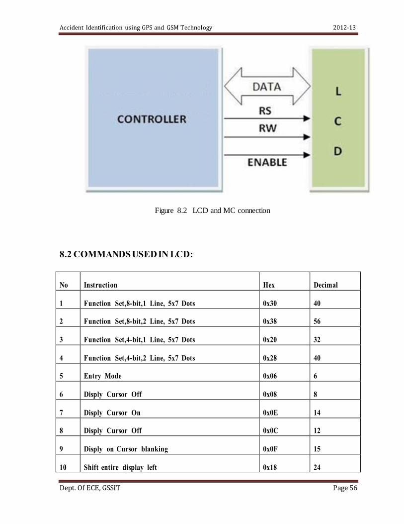
Accident Identification using GPS and GSM Technology 2012-13
Dept. Of ECE, GSSIT Page 56
Figure 8.2 LCD and MC connection
8.2 COMMANDS USED IN LCD:
No Instruction Hex Decimal
1 Function Set,8-bit,1 Line, 5x7 Dots 0x30 40
2 Function Set,8-bit,2 Line, 5x7 Dots 0x38 56
3 Function Set,4-bit,1 Line, 5x7 Dots 0x20 32
4 Function Set,4-bit,2 Line, 5x7 Dots 0x28 40
5 Entry Mode 0x06 6
6 Disply Cursor Off 0x08 8
7 Disply Cursor On 0x0E 14
8 Disply Cursor Off 0x0C 12
9 Disply on Cursor blanking 0x0F 15
10 Shift entire display left 0x18 24

Accident Identification using GPS and GSM Technology 2012-13
Dept. Of ECE, GSSIT Page 57
11 Shift entire display right 0x1C 30
12 Move Cursor left by one character 0x10 16
13 Move Cursor right by one character 0x14 20
14 Clear Display 0x01 1
Table 8.2 LCD commands

Accident Identification using GPS and GSM Technology 2012-13
Dept. Of ECE, GSSIT Page 58
CHAPTER 9
RELAY CIRCUIT
A relay is an electrically operated switch used to isolate one electrical circuit from
another. In its simplest form, a relay consists of a coil used as an electromagnet to open and
close switch contacts. Since the two circuits are isolated from one another, a lower voltage
circuit can be used to trip a relay, which will control a separate circuit that requires a higher
voltage or amperage. Relays can be found in early telephone exchange equipment, in industrial
control circuits, in car audio systems, in automobiles, on water pumps, in high-power audio
amplifiers and as protection devices.
9.1 Single Pole Double Throw Relay
A single pole double throw (SPDT) relay configuration switches one common pole to
two other poles, flipping between them. As shown in the schematic diagram, the common point
E completes a circuit with C when the relay coil is at rest, that is, no voltage is applied to it.
This circuit is "closed." A gap between the contacts of point E and D creates an "open" circuit.
When you apply power to the coil, a metal level is pulled down, closing the circuit between
points E and D and opening the circuit between E and C. A single pole double throw relay can
be used to alternate which circuit a voltage or signal will be sent to.
SPDT Relay
Single Pole Double Throw Relay an electromagnetic switch , consist of a coil and 1
common terminal, 1 normally closed terminal, and one normally open terminal.When the coil of
an SPDT relay is at rest , the common terminal and the normally closed terminal have a
continuity . When the coil is energized, the common terminal and the normally open terminal
have continuity.
The diagram below center shows an SPDT relay at rest,with the coil not energized. The
diagram below right shows the relay with the coil energized. As you can see, the coil is an
electromagnet that causes the arm that is always broken form the normally closed terminal and
made with the normally open terminal.
When energizing the coil of a relay, polarity of the coil does not matter unless there is a
diode across the coil. If a diode is not present, you may attach positive voltage to either terminal

Accident Identification using GPS and GSM Technology 2012-13
Dept. Of ECE, GSSIT Page 59
of the coil and negative voltage to the other, otherwise you may attach positive to the side of the
coil that the cathode side of the diode is connected and negative side of the coil that the anode
ide of the diode is connected.
Figure 9.1 SPDT relay switch with PIN Numbers
The need for SPDT in our project (model) is that, whenever we want to
switch a device that draws more current you will need to use relay. The coil draws
less current and the current which flows through common, normally closed
,normally open contacts will handle up to 30 or 40 amperes.

Accident Identification using GPS and GSM Technology 2012-13
Dept. Of ECE, GSSIT Page 60
CHAPTER 10
Temperature Sensor (LM35).
LM35 is a precision IC temperature Sensor with its output proportional to the
temperature. The sensor circuitry is sealed and therefore it is not subjected to
oxidation and other process. With LM35, temperature can be measured more
accurately than a thermistor. It also possess low self heating and does not cause
more than 0.1 oC temperature rise in still air.
Figure 10.1 Pin diagram
Pin NO Function Name
1 Supply Volatge;5v(+35 to -2v)) Vcc
2 Output Voltage(+6v to -1v) Output
3 Ground Ground
Table 10.1 Pin Description
Features
Calibrated directly in ˚ Celsius (Centigrade) n Linear + 10.0
mV/˚C scale factor.
0.5˚C accuracy guaranteeable (at +25˚C) n Rated for full
−55˚ to +150˚C range
Suitable for remote applications
Low cost due to wafer-level trimming

Accident Identification using GPS and GSM Technology 2012-13
Dept. Of ECE, GSSIT Page 61
Operates from 4 to 30 volts
Less than 60 µA current drain
Low self-heating, 0.08˚C in still air
Nonlinearity only ± 1⁄4˚C typical
Low impedance output, 0.1 W for 1 mA load
It has an output proportional to the Celsius temperature. The scale factor is 0.01V/ oC .
The LM35 does not require any calibration and maintain an good accuracy at room
temperature. It draws on 60 micro amps from its supply and possesses a low self-heating
capability. The sensor self- heating causes less than 0.1 oC temperature rise in air. The output of
the Sensor is analog output, hence it is further connected to ADC for intimation through
Microcontroller.
Figure 10.2 Functional Block Diagram

Accident Identification using GPS and GSM Technology 2012-13
Dept. Of ECE, GSSIT Page 62
CHAPTER 11
L293D (Driver IC)
L293D is a dual H-bridge motor driver integrated circuit (IC). Motor drivers act as
current amplifiers since they take a low-current control signal and provide a higher-current
signal. This higher current signal is used to drive the motors.
L293D contains two inbuilt H-bridge driver circuits. In its common mode of
operation, two DC motors can be driven simultaneously, both in forward and reverse
direction.
The microcontroller is driven by a 5V voltage from the regulator. Hence it cannot
control the DC motor whose operating voltage is 12V. The Drive IC acts as an amplifier and
send the 12V Dc supply to the motors connected to the wheel.
The motor operations of two motors can be controlled by input logic at pins 2 & 7
and 10 & 15. Input logic 00 or 11 will stop the corresponding motor. Logic 01 and 10 will
rotate it in clockwise and anticlockwise directions, respectively.
Enable pins 1 and 9 (corresponding to the two motors) must be high for motors to
start operating. When an enable input is high, the associated driver gets enabled. As a result,
the outputs become active and work in phase with their inputs. Similarly, when the enable
input is low, that driver is disabled, and their outputs are off and in the high-impedance state.
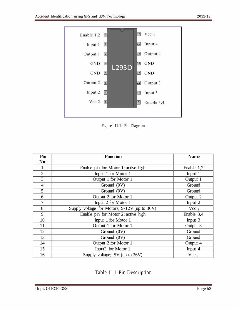
Accident Identification using GPS and GSM Technology 2012-13
Dept. Of ECE, GSSIT Page 63
Figure 11.1 Pin Diagram
Pin
No Function Name
1 Enable pin for Motor 1; active high Enable 1,2
2 Input 1 for Motor 1 Input 1
3 Output 1 for Motor 1 Output 1
4 Ground (0V) Ground
5 Ground (0V) Ground
6 Output 2 for Motor 1 Output 2
7 Input 2 for Motor 1 Input 2
8 Supply voltage for Motors; 9-12V (up to 36V) Vcc 2
9 Enable pin for Motor 2; active high Enable 3,4
10 Input 1 for Motor 1 Input 3
11 Output 1 for Motor 1 Output 3
12 Ground (0V) Ground
13 Ground (0V) Ground
14 Output 2 for Motor 1 Output 4
15 Input2 for Motor 1 Input 4
16 Supply voltage; 5V (up to 36V) Vcc 1
Table 11.1 Pin Description
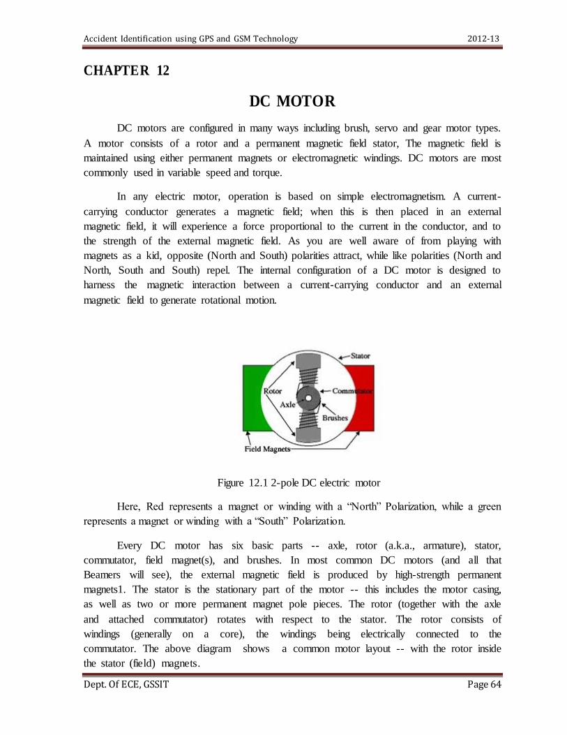
Accident Identification using GPS and GSM Technology 2012-13
Dept. Of ECE, GSSIT Page 64
CHAPTER 12
DC MOTOR
DC motors are configured in many ways including brush, servo and gear motor types.
A motor consists of a rotor and a permanent magnetic field stator, The magnetic field is
maintained using either permanent magnets or electromagnetic windings. DC motors are most
commonly used in variable speed and torque.
In any electric motor, operation is based on simple electromagnetism. A current-
carrying conductor generates a magnetic field; when this is then placed in an external
magnetic field, it will experience a force proportional to the current in the conductor, and to
the strength of the external magnetic field. As you are well aware of from playing with
magnets as a kid, opposite (North and South) polarities attract, while like polarities (North and
North, South and South) repel. The internal configuration of a DC motor is designed to
harness the magnetic interaction between a current-carrying conductor and an external
magnetic field to generate rotational motion.
Figure 12.1 2-pole DC electric motor
Here, Red represents a magnet or winding with a “North” Polarization, while a green
represents a magnet or winding with a “South” Polarization.
Every DC motor has six basic parts -- axle, rotor (a.k.a., armature), stator,
commutator, field magnet(s), and brushes. In most common DC motors (and all that
Beamers will see), the external magnetic field is produced by high-strength permanent
magnets1. The stator is the stationary part of the motor -- this includes the motor casing,
as well as two or more permanent magnet pole pieces. The rotor (together with the axle
and attached commutator) rotates with respect to the stator. The rotor consists of
windings (generally on a core), the windings being electrically connected to the
commutator. The above diagram shows a common motor layout -- with the rotor inside
the stator (field) magnets.
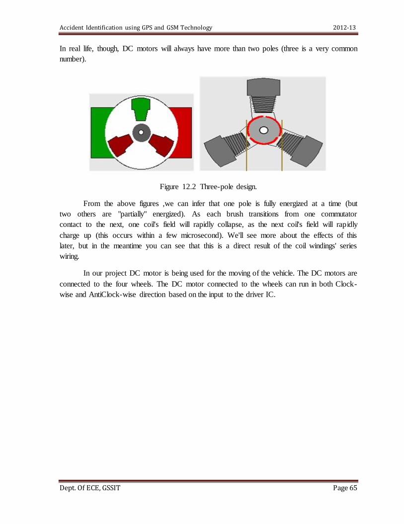
Accident Identification using GPS and GSM Technology 2012-13
Dept. Of ECE, GSSIT Page 65
In real life, though, DC motors will always have more than two poles (three is a very common
number).
Figure 12.2 Three-pole design.
From the above figures ,we can infer that one pole is fully energized at a time (but
two others are "partially" energized). As each brush transitions from one commutator
contact to the next, one coil's field will rapidly collapse, as the next coil's field will rapidly
charge up (this occurs within a few microsecond). We'll see more about the effects of this
later, but in the meantime you can see that this is a direct result of the coil windings' series
wiring.
In our project DC motor is being used for the moving of the vehicle. The DC motors are
connected to the four wheels. The DC motor connected to the wheels can run in both Clock-
wise and AntiClock-wise direction based on the input to the driver IC.
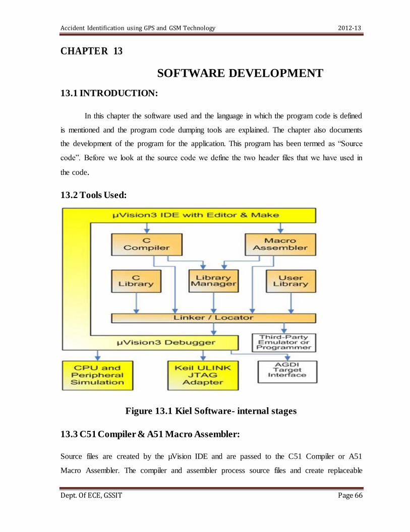
Accident Identification using GPS and GSM Technology 2012-13
Dept. Of ECE, GSSIT Page 66
CHAPTER 13
SOFTWARE DEVELOPMENT
13.1 INTRODUCTION:
In this chapter the software used and the language in which the program code is defined
is mentioned and the program code dumping tools are explained. The chapter also documents
the development of the program for the application. This program has been termed as “Source
code”. Before we look at the source code we define the two header files that we have used in
the code.
13.2 Tools Used:
Figure 13.1 Kiel Software- internal stages
13.3 C51 Compiler & A51 Macro Assembler:
Source files are created by the µVision IDE and are passed to the C51 Compiler or A51
Macro Assembler. The compiler and assembler process source files and create replaceable

Accident Identification using GPS and GSM Technology 2012-13
Dept. Of ECE, GSSIT Page 67
object files. The Keil C51 Compiler is a full ANSI implementation of the C programming
language that supports all standard features of the C language. In addition, numerous features
for direct support of the 8051 architecture have been added.
13.4 µVISION:
µVision3 adds many new features to the Editor like Text Templates, Quick Function
Navigation, and Syntax Coloring with brace high lighting Configuration Wizard for dialog
based startup and debugger setup. µVision3 is fully compatible to µVision2 and can be used in
parallel with µVision2.
µVision3 is an IDE (Integrated Development Environment) that helps you write, compile, and
debug embedded programs. It encapsulates the following components:
A project manager.
A make facility.
Tool configuration.
Editor.
A powerful debugger.
13.5 BUILDING AN APPLICATION IN µVISION
To build (compile, assemble, and link) an application in µVision2, you must:
1. Select Project -(forexample,166\EXAMPLES\HELLO\HELLO.UV2).
2. Select Project - Rebuild all target files or Build target.µVision2 compiles,
assembles, and links the files in your project.
Creating Your Own Application in µVision2:
To create a new project in µVision2, you must:
1. Select Project - New Project.
2. Select a directory and enter the name of the project file.
3. Select Project - Select Device and select an 8051, 251, or C16x/ST10 device
from the Device Database™.

Accident Identification using GPS and GSM Technology 2012-13
Dept. Of ECE, GSSIT Page 68
4. Create source files to add to the project.
5. Select Project - Targets, Groups, Files. Add/Files, select Source Group1, and
add the source files to the project.
6. Select Project - Options and set the tool options. Note when you
select the target device from the Device Database™ all special
options are set automatically. You typically only need to configure
the memory map of your target hardware. Default memory model
settings are optimal for most applications.
7. Select Project - Rebuild all target files or Build target.
Debugging an Application in µVision2:
To debug an application created using µVision2, you must:
1. Select Debug - Start/Stop Debug Session.
2. Use the Step toolbar buttons to single-step through your program. You may
enter G, main in the Output Window to execute to the main C function.
3. Open the Serial Window using the Serial #1 button on the toolbar. Debug your
program using standard options like Step, Go, Break, and so on.
Starting µVision2 and creating a Project
µVision2 is a standard Windows application and started by clicking on the
program icon. To create a new project file select from the µVision2 menu
Project –
New Project…. This opens a standard Windows dialog that asks you for the new
project file name. We suggest that you use a separate folder for each project. You can
simply use the icon Create New Folder in this dialog to get a new empty folder. Then
select this folder and enter the file name for the new project, i.e. Project1. µVision2
creates a new project file with the name PROJECT1.UV2 which contain default target
and file group name. You can see these names in the Project

Accident Identification using GPS and GSM Technology 2012-13
Dept. Of ECE, GSSIT Page 69
Window - Files.
Now use from the menu Project - Select Device for Target and select a CPU
for your project. The Select Device dialog box shows the µVision2 device database. Just
select the microcontroller you use. We are using for our examples the Philips
80C51RD+ CPU. This selection sets necessary tool options for the 80C51RD+ device
and simplifies in this way the tool Configuration
Building Projects and Creating a HEX Files
Typical, the tool settings under Options - Target are all you need to start a new
application. You may translate all source files and line the application with a click on the Build
Target toolbar icon. When you build an application with syntax errors, µVision2 will display
errors and warning messages in the Output Window - Build page. A double click on a message
line opens the source file on the correct location in a µVision2 editor window. Once you have
successfully generated your application you can start debugging.
After you have tested your application, it is required to create an Philips HEX file to download
the software into an EPROM programmer or simulator. µVision2 creates HEX files with each
build process when Create HEX files under Options for Target - Output is enabled. You may
start your PROM programming utility after the make process when you specify the program
under the option Run User Program #1.
CPU Simulation
µVision2 simulates up to 16 Mbytes of memory from which areas can be mapped for read,
write, or code execution access. The µVision2 simulator traps and reports illegal memory
access . In addition to memory mapping, the simulator also provides support for the integrated
peripherals of the various 8051 derivatives. The on-chip peripherals of the CPU you have
selected are configured from the Device
Database selection
You have made when you create your project target. Refer page 58 for more
Information about selecting a device. You may select and display the on-chip peripheral

Accident Identification using GPS and GSM Technology 2012-13
Dept. Of ECE, GSSIT Page 70
components using the Debug menu. You can also change the aspects of each peripheral using
the controls in the dialog boxes.
Start Debugging
You start the debug mode of µVision2 with the Debug - Start/Stop Debug Session
command. Depending on the Options for Target - Debug Configuration, µVision2 will load the
application program and run the startup code µVision2 saves the editor screen layout and
restores the screen layout of the last debug session. If the program execution stops, µVision2
opens an editor window with the source text or shows CPU instructions in the disassembly
window. The next executable statement is marked with a yellow arrow. During debugging,
most editor features are still available.
For example, you can use the find command or correct program errors. Program source text of
your application is shown in the same windows. The µVision2 debug mode differs from the
edit mode in the following aspects:
The “Debug Menu and Debug Commands” described below are available. The additional
debug windows are discussed in the following. The project structure or tool parameters cannot
be modified. All build Commands are disabled.
Disassembly Window
The Disassembly window shows your target program as mixed source and assembly program
or just assembly code. A trace history of previously executed instructions may be displayed
with Debug - View Trace Records. To enable the trace history set Debug Enable/Disable
Trace Recording.
If you select the Disassembly Window as the active window all program step commands work
on CPU instruction level rather than program source lines. You can select a text line and set or
modify code breakpoints using toolbar buttons or the context menu commands.
You may use the dialog Debug - Inline Assembly… to modify the CPU instructions. That
allows you to correct mistakes or to make temporary changes to the target program you are
debugging.
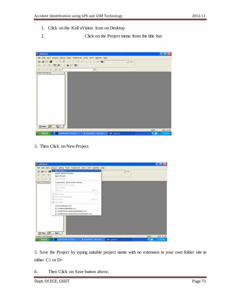
Accident Identification using GPS and GSM Technology 2012-13
Dept. Of ECE, GSSIT Page 71
1. Click on the Keil uVision Icon on Desktop
2. . Click on the Project menu from the title bar
3. Then Click on New Project.
5. Save the Project by typing suitable project name with no extension in your own folder site in
either C:\ or D:\
6. Then Click on Save button above.

Accident Identification using GPS and GSM Technology 2012-13
Dept. Of ECE, GSSIT Page 72
7. Select the component for your project. i.e. NXP or Philips
8. Click on the + Symbol beside of NXP
9. Select P89V51RD2FN as shown below
10. Then Click on “OK”
11. The Following fig will appear
12. Then Click either YES or NO………mostly “NO”
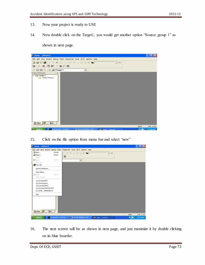
Accident Identification using GPS and GSM Technology 2012-13
Dept. Of ECE, GSSIT Page 73
13. Now your project is ready to USE
14. Now double click on the Target1, you would get another option “Source group 1” as
shown in next page.
15. Click on the file option from menu bar and select “new”
16. The next screen will be as shown in next page, and just maximize it by double clicking
on its blue boarder.
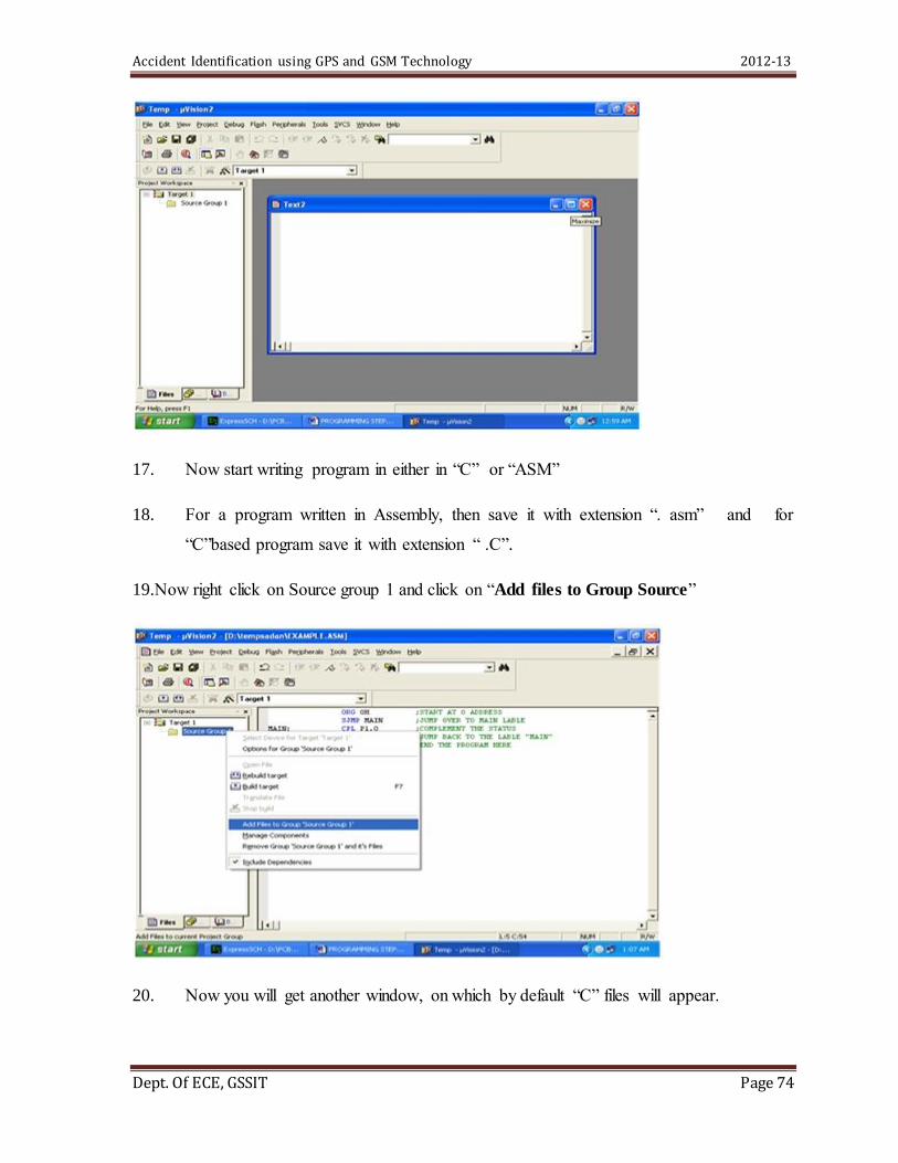
Accident Identification using GPS and GSM Technology 2012-13
Dept. Of ECE, GSSIT Page 74
17. Now start writing program in either in “C” or “ASM”
18. For a program written in Assembly, then save it with extension “. asm” and for
“C”based program save it with extension “ .C”.
19.Now right click on Source group 1 and click on “Add files to Group Source”
20. Now you will get another window, on which by default “C” files will appear.

Accident Identification using GPS and GSM Technology 2012-13
Dept. Of ECE, GSSIT Page 75
21. Now select as per your file extension given while saving the file
22. Click only one time on option “ADD”
23. Now Press function key F7 to compile. Any error will appear if so happen.
24. If the file contains no error, then press Control+F5 simultaneously.
25. The new window is as follows.
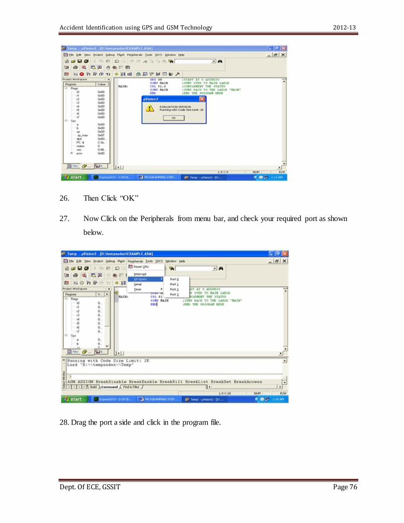
Accident Identification using GPS and GSM Technology 2012-13
Dept. Of ECE, GSSIT Page 76
26. Then Click “OK”
27. Now Click on the Peripherals from menu bar, and check your required port as shown
below.
28. Drag the port a side and click in the program file.
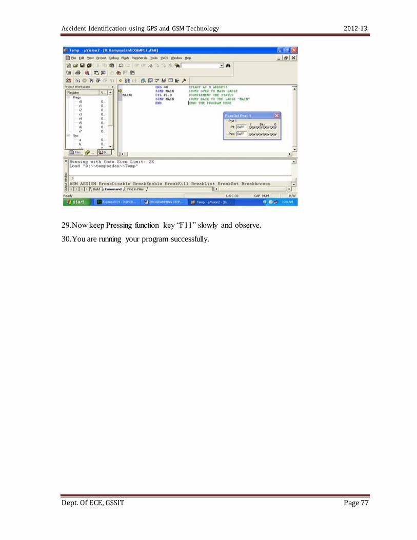
Accident Identification using GPS and GSM Technology 2012-13
Dept. Of ECE, GSSIT Page 77
29.Now keep Pressing function key “F11” slowly and observe.
30.You are running your program successfully.
Accident Identification using GPS and GSM Technology 2012-13
Dept. Of ECE, GSSIT Page 78
CHAPTER 14
ADVANTAGES AND DISADVANTAGES
14.1 Advantages
The vehicle which is undergone through an accident can be identified by using tracking
technology without any delay.
The immediate medication or the first aid will be provided to the victims in remote
areas.
Allows the remote locations of asset from anywhere there is cellular service.
A low cost Vehicle tracking with accident identification system can reduce the fatalities
during accidents.
Can avoid misusage of the vehicle thereby reducing fuel consumption.
14.2 Disadvantages
The anti GPS tracker disrupter if installed will knock out GPS logging or GPS tracking
system which may be operating on a vehicle, using GPS disrupter system will make it
very hard for anyone to keep tabs on a vehicle.
If a vehicle is out of reach of the network then this tracking can‟t be done.
It may misused for tracking a VIP vehicle for destructive purposes .
If the GSM module gets damaged during the accident the message intimation can‟t be
sent.

Accident Identification using GPS and GSM Technology 2012-13
Dept. Of ECE, GSSIT Page 79
CONCLUSION
This version of our project will send a reply when we send a SMS and also sends the
position of the vehicle in terms of latitude and longitude when there is any accident. It doesn„t
tell the exact nature of the accident, whether it is severe or just a mild one. With the help of
accelerometer sensor, we can tell the exact position of the vehicle. We can predict whether the
vehicle is in normal position or upside down.
This project can be enhanced in future by modifying in the program to find out the
actual position of the vehicle and also in accident prevention. This can also be enhanced by
automatically locking all the brakes in case of accident. In many accidents, it becomes severe
as the drivers lose control and can„t stop the vehicle. During the accident, the accelerometer
sensor will triggered due to vibrations which is received and processed by the Spartan
processor. The processor should be connected to devices which can lock the brakes when
triggered. By this enhancement, we can stop the vehicle and can reduce the impact of the
accident.
This can be used to prevent vehicle theft. In case of any theft, the owner can track the
location of the vehicle.
In public transport system, the implementation of this equipment will ease the people.
When public transport systems like bus, trains these are installed with this equipment, People
can know the location of the vehicle and arrive in the stop in time. Modifying the code, we can
make it to send the position of the vehicle periodically to a subscribed mobile number so that
companies can keep an eye on their vehicles.
Thus we can make use of the available technology to the benefit of the people by
saving the lives of the people and helping the owners of the vehicle to keep track of their
vehicles.

Accident Identification using GPS and GSM Technology 2012-13
Dept. Of ECE, GSSIT Page 80
BIBLIOGRAPHY
[1].THE 8051 MICROCONTROLLER AND EMBEDDED SYSTEMS , Using Assemby and
C , Muhammad Ali Mazidi , Janice Gillispie, Rolin D.McKinlay, Second Edition 2008.
[2]. The 8051 Micro controller Architecture,Programming & Applications – Kenneth J Ayala.
REFERENCES ON THE WEB
[1]. http://www.engineersgarage.com/
[2]. http://www.datasheetarchive.com/simcom-datasheet.html.
[3]. http://www.datasheetcatalog.com/philips/1/
[4]. http://www.8051projects.info/projects.asp
[5]. http://en.wikipedia.org/wiki/Global_Positioning_System
[6]. http://www.8051projects.info/