ace™ automated circuit extraction - armms · ace™ automated circuit extraction ... extraction...
TRANSCRIPT

Andy Wallace Paper 9: Page 1 of 11 ARMMS Nov 2007
ACE™ Automated Circuit Extraction
Andy Wallace and Mike Heimlich Email: [email protected]
Applied Wave Research Ltd (Europe), 2 Huntingate, Hitchin, Herts, UK. SG4 0TJ
Abstract
This paper provides an introduction to ACE™ Automated Circuit Extraction technology from Applied Wave
Research, Inc. (AWR®). ACE™ is an innovative approach to avoid the over dependence of EM analysis as
a design tool. The ACE™ software automates the modeling of complex interconnect structures defined as
paths by assembling their equivalent electrical models on-the-fly using the very same network representation
designers themselves would make use of if they had the time and patience to do so. The simulation of the
equivalent circuit is done in a fraction of the time that it would take EM tools to create equivalent
S-parameters. The speed, accuracy, and parametric nature of ACE™ software enable engineers to return to
real design by exploring design alternatives and changes in seconds. Obviously, EM verification is still a
necessary part of the flow, but the ACE™ tool enables engineers to design once again rather than analyze
after the event, even on many of the most challenging RF and MW designs.
Introduction Today’s traditional approach to RF and/or Microwave circuit design is being pressured simultaneously by an
increase in operating frequencies and bandwidth and a decrease in physical footprint size. The result is that
the physical design challenges faced by these designers are rapidly increasing, while choices for how these
challenges should be best addressed are not. The drive to put more functionality into the same or smaller
space is particularly demanding on the RF/Microwave design flow because of the increased and unavoidable
need to model interconnects and their interactions. Ideally, modeling all of the interactions at the schematic
level using distributed line, discontinuity, coupled-line models and vias is preferred. While there is nothing
preventing an engineer from doing this, the complexity of modern wireless designs makes this an unrealistic
and unreasonable approach at a schematic level, given that this manual process is incredibly time consuming
and error prone. Figure 1 shows a very simple section of PCB multi-layer interconnects, minus the SMT
components !
Figure 1: Simple section of PCB multi-layer interconnect showing coupled line structure
with bend discontinuities and via holes
W1
W2
W3
W4
W5
W6
1
2
3
4
5
6
7
8
9
10
11
12
GM6CLINID=TL1W1=20 um
W2=20 umW3=20 umW4=20 umW5=20 umW6=20 umOffs1=40 um
Offs2=40 umOffs3=40 umOffs4=40 umOffs5=40 umOffs6=40 umCL1=1
CL2=1CL3=1CL4=1CL5=1CL6=1L=40 um
Acc=1
W1
W2
W3
W4
W5
1
2
3
4
5
6
7
8
9
10
GM5CLIN
ID=TL2W1=20 umW2=20 umW3=20 umW4=20 umW5=20 um
Offs1=40 umOffs2=40 umOffs3=40 umOffs4=40 umOffs5=40 umCL1=1
CL2=1CL3=1CL4=1CL5=1L=40 umAcc=1
W1
W2
W3
W4
1
2
3
4
5
6
7
8
GM4CLINID=TL3W1=20 umW2=20 um
W3=20 umW4=20 umOffs1=40 umOffs2=40 umOffs3=40 umOffs4=40 um
CL1=1CL2=1CL3=1CL4=1L=40 umAcc=1
VIAID=V1D=20 umH=100 um
T=2 umRHO=1
VIA
ID=V2D=20 umH=100 umT=2 umRHO=1
VIAID=V3D=20 umH=100 umT=2 um
RHO=1
VIAID=V4D=20 um
H=100 umT=2 umRHO=1
VIA
ID=V5D=20 umH=100 umT=2 umRHO=1
VIAID=V6D=20 umH=100 umT=2 um
RHO=1
VIAID=V7D=20 um
H=100 umT=2 umRHO=1
VIA
ID=V8D=20 umH=100 umT=2 umRHO=1
W1
W2
W3
W4
W5
1
2
3
4
5
6
7
8
9
10GM5CLINID=TL4W1=20 umW2=20 um
W3=20 umW4=20 umW5=20 umOffs1=40 umOffs2=40 umOffs3=40 um
Offs4=40 umOffs5=40 umCL1=1CL2=1CL3=1CL4=1
CL5=1L=40 umAcc=1
ML INID=TL5W=20 umL =40 u m
MLINID=TL6W=20 umL=40 um
MBEND90X$ID=MS1M=0
MBEND90X$ID=MS2M= 0
MBEND90X$
ID=MS3M=0
MBEND90X$ID=MS4
M=0
MLINID=TL7W=20 umL=40 um
MLINID=TL8W=20 umL=40 um

Andy Wallace Paper 9: Page 2 of 11 ARMMS Nov 2007
Consequently, the engineer’s response has been to forego detailed schematic level design and go straight to
analysis and verification as a weak, but faster, alternative after final layout. While this method saves
engineering time by avoiding the manual insertion of various RF and Microwave line models, the trade-off is
that the overall engineering time grows as the analysis and verification burden for using EM as a design tool
has mushroomed. The reality has unfortunately become infinite “layout & EM analysis” cycles as lines are
moved and vias replaced. This is all being done without any design engineering methodology, first principles
insight, or a parametric handle into or behind the reasons for doing so.
This situation is all the more critical when considering that by the time a layout is complete enough to do this
sort of “layout & EM analysis” cycle, the design is much closer to the end of its cycle than the beginning.
Study after study on the engineering of complex systems, from spacecraft to software to electronics, shows
that it is much more cost-effective to identify and fix design deficiencies as early as possible in the design
cycle. However, doesn’t this mean that the improper use of EM as a design tool makes this a costly and risky
proposition to many RF and Microwave design flows?
EDA developers are working to “catch-up” with the multitude of design challenges created by the exploding
wireless communications market. This paper describes the new ACE™ technology and discusses real-world
design examples where this new software approach provides an accurate, efficient, modern methodology as
an alternative to traditional RF and Microwave design approaches that no longer meet the challenges of next-
generation communications product design.
What is ACE™?
ACE™ Automated Circuit Extraction technology from Applied Wave Research, Inc. (AWR®) is an
innovative response to the overuse of EM as a design tool. ACE™ software reclaims parametric design for
the user by creating netlist-based representations of complex interconnects using the very same networks of
parametric models designers themselves would use if they had the time and patience to do so, in a fraction of
the time that it would take EM tools to create equivalent S-parameters. The speed, accuracy, and parametric
nature of ACE™ software enable engineers to return to real design by exploring design alternatives and
changes in seconds. Obviously, EM verification is still a necessary part of the flow, but the ACE™ tool
enables engineers to design once again rather than analyze, even on many of the most challenging RF and
MW designs.
ACE™ software is based on the proven digital and analog-mixed signal (AMS) technique of circuit
extraction from physical layout, but uses microwave models and principles. The tool puts the engineer back
into the driver’s seat of design by creating circuit models from layout geometries. The ACE™ tool, like all
circuit extractors, creates a model for interconnects by geometrically analyzing a layout through breaking it
down into pieces that the extractor understands, mapping each piece of the reduced geometry to a model, and
then combining the models intelligently to create a simulatable representation. Digital and AMS extractors
typically use RLCK models shown in Figure 2 to model interconnect-reduced geometries, but these require
very dense networks at microwave frequencies to capture dispersion and skin-effect and they tend to be
bandwidth limited.

Andy Wallace Paper 9: Page 3 of 11 ARMMS Nov 2007
Figure 2: RLCK models for a dispersive microwave transmission line used by digital and AMS extractors
ACE™ software, on the other hand, views the layout in terms of distributed line, coupled-line, and
discontinuity models that microwave engineers have been using for years, such as MLIN/SLIN,
MTEE/STEE, and M2CLIN/S2CLIN, and so dispersion, skin-effect, and bandwidth are non-issues.
Moreover, vias can be modelled with S-parameter files from pre-defined via libraries, a fixed resistance or an
AWR VIA model.
The ACE™ tool generates a detailed, extensive netlist shown in Figure 3 in seconds for complex
arrangements of interconnects that engineers would prefer to make, but either don’t have the hours or days to
do it or find it too error-prone. EM analysis would take days or even weeks for a single design iteration,
provided the computer hardware didn’t crash.
Figure 3: ACE™ extracted netlist from a multi layer board design.
K
K
K
K
K
KK
KK
KK
KK
KK

Andy Wallace Paper 9: Page 4 of 11 ARMMS Nov 2007
ACE™ software goes even a few steps further than this. As part of the way in which it views the schematics,
the same ground planes that are assumed for substrate definitions are found and simplified so that lines
separated by a ground plane are not grouped together in a coupled line structure. Even with low temperature
co-fired ceramic (LTCC) materials, where dielectric constant and thickness may vary, ACE™ software
defines on-the-fly substrate definitions for the distributed models it extracts. Also, for lines that crossover on
different layers not separated by a ground plane, a coupling capacitor is calculated based on geometry. To
obtain the highest degree of accuracy, the ACE™ tool can even be directed to extract geometries to models,
which themselves have highly optimized, built-in, EM solvers. In many cases, the software can provide
accuracy that is similar to EM analysis, but is hundreds if not thousands of times faster for design tasks early
and throughout the design flow.
The ACE™ technology uses all of the schematic level models designers would use to model complex
interconnects if they had the time and the patience. For fast, efficient, and accurate answers it uses closed-
form models such as MLIN and SLIN for lines, MTEE for t-junctions, and M2CLIN for coupled lines.
Without sacrificing speed, AWR’s industry-leading X-models (EM table-based models with the accuracy of
EM and the speed of closed-form models) can be used for discontinuities. For the most accurate answers,
designers can direct the ACE™ tool to use models that have finite element method (FEM) solvers built right
in with the model that are highly optimized to solve that particular geometry. GFMCLIN, for example, has an
FEM solver inside, which turns the parametric descriptions into geometries solved by its FEM solver in a
fraction of the time of generalized, three-dimensional (3D) FEM tools. Designers now have the choice to
trade off the difference between speed and degree of accuracy when they chose to have ACE™ use method-
of-moments (MoM) solvers -- faster than the FEM-based circuit models such as GFMCLIN and more
accurate than the closed-form models such as M2CLIN.
Example 1 – MMIC Distributed Amplifier A monolithic microwave integrated circuit (MMIC) distributed amplifier depends on the inter-stage
interconnects to define its impedance and bandwidth characteristics. Figure 4 shows such a design using
pseudomorphic high electron mobility transistor (PHEMT) technology initially modeling the interconnects
with distributed MLIN, MBEND, MTEE, etc. models, but, for example, no coupling among adjacent arms of
the meandered inter stage lines.
Using ACE™ software with a very large coupling distance specified yields greater bandwidth, but at the
expense of gain flatness; the culprit is the couplings, shown in extracted schematic form in Figure 5.

Andy Wallace Paper 9: Page 5 of 11 ARMMS Nov 2007
Figure 4: Distributed amplifier with ACE™ to extract distributed and discontinuity models with no
interconnect couplings. Extraction time is ~ 0.5 seconds for DC to 12GHz
Figure 5: ACE™ software with large coupling distance showing performance degradation.
Extraction time is approximately 1 second for DC to 12GHz

Andy Wallace Paper 9: Page 6 of 11 ARMMS Nov 2007
By reducing the ACE™ coupling distance, it can be seen that majority of the detrimental coupling is due to
the adjacent arms of the meandered interconnects highlighted in Figure 6.
Figure 6: Reduced ACE™ coupling radius (bold traces, left) reveals overall performance degradation
(gray traces, left) mainly due to adjacent couplings (red circles, right)
In a matter of minutes, the ACE™ technology empowers the designer to identify, pinpoint, and redesign
the circuit as appropriate, whereas iterating cycles with layout and EM analysis would likely take the
better part of a day or days.
RF-Style Interconnects: iNets®
In the above example, the interconnects and meander lines were drawn from a microwave engineers point of
view – explicit MLIN’s, t-junctions and MBENDS. With just a little more effort, the parallel segments could
easily be changed to coupled-line models and similar results obtained without the need for ACE™. To extort
the real benefit, AWR have introduced iNets® technology – intelligent nets. This technology gives the
designer the ability to draw a simple short circuit interconnect in the electrical schematic diagram and then in
the layout, route that interconnect with the internal knowledge of the technology being used. For example,
on a four layer PCB, the five possible locations of the track along with the customer specific via hole options
are offered during the routing process. These are all DRC correct against the given technology (GaAs,
LTCC, Duroid, PCB, Si, and SiGe) and result in a manufacturable interconnect in the layout world. Using
ACE™, this physical layout can now produce an advanced netlist, which when combined with the schematic
electrical design of real components, provides incredibly accurate simulation results.
To show iNets® on a simple design, I refer to the RLC schematic in Figure 7. The graph shows the
expected RLC response of the grey trace when the ACE™ extraction is disabled, and the ripple and loss
in blue as expected from the long meandered iNets® drawn in the layout. These iNets® viewed in 3D,
show that the immense detail required for manufacture can easily be produced with an appropriate
technology file, and a few mouse clicks to route the interconnect.
0 2 4 6 8 10 12
Frequency (GHz)
Gain and S11 and S22
-30
-20
-10
0
10
20
Ma
gn
itu
de
(d
B)
8 GHz9.433 dB
5 GHz11.17 dB
2 GHz12.15 dB
Gain = |S(2,1)| |S(1,1)| |S(2,2)|
0 2 4 6 8 10 12
Frequency (GHz)
Gain and S11 and S22
-30
-20
-10
0
10
20
Ma
gn
itu
de
(d
B)
8 GHz9.433 dB
5 GHz11.17 dB
2 GHz12.15 dB
Gain = |S(2,1)| |S(1,1)| |S(2,2)|

Andy Wallace Paper 9: Page 7 of 11 ARMMS Nov 2007
Figure 7: iNets® for a very simple RLC circuit, showing immense detail in 3D for manufacturing
Example 2 – MMIC Spiral Coupling Making use of iNets® coupled with ACE™ extraction technology, the design cycle for complex
Microwave designs reduces from hours to minutes. Two identical designs, shown below in Figure 8
have close to identical layout – trace chamfered corners being the major difference. Explicit microwave
circuit element design has now been replaced with the much simpler RF approach in terms of schematic
circuit level entry coupled with iNets® technology producing an identical layout. Once extracted through
ACE™, the simulation results are incredibly similar as per Figure 9 but with the benefit in a hugely reduced
design time.
ACE™ can be pushed yet further with designs that now include previously un-simulated reactions. In the
same single stage amplifier design, we add a second spiral inductor into the schematic diagram using iNets®
which is completely isolated from the original circuit in the electrical schematic. With ACE™ extraction in
Figure 10, cross coupling due to the physical layout and spiral proximity now perturbs the original
simulation results allowing the design engineer to ensure this effect is accounted for during the very first
design cycle at the simulation stage before costly prototyping.

Andy Wallace Paper 9: Page 8 of 11 ARMMS Nov 2007
Figure 8: Identical circuits with very similar layout – one taking minutes, the other hours
1 3 5 7 9 10
Frequency (GHz)
Amplifier S21
10
12
14
16
18
DB(|S(2,1)|)Amplifier RF
DB(|S(2,1)|)Amplifier Microwave
Figure 9: Simulation accuracy using traditional design versus ACE™ Extraction

Andy Wallace Paper 9: Page 9 of 11 ARMMS Nov 2007
Figure 10: Cross Coupling of a second Spiral Inductor, drawn as an iNet®
and the resulting change in simulation response
Example 3 –Printed Circuit Board (PCB) Design
In this final example, ACE™ capabilities are applied to a complex, 16-layer PCB application shown in
Figure 11 early in the design flow in order to efficiently and accurately design the RF transmit signal path on
the top side of the board alongside digital control on the bottom side and ground planes in between layers.
All in all, at this stage of the design, the 16-layer board has 168 nets and therefore 336 ports, dozens of vias –
some blind, some buried and some though vias and yet a simple schematic circuit with the routes being
generated in the layout world.
Analyzing this large a design with a 3D planar solver is a time-consuming task because of the time required
to create the Green’s function for the multiple, non-uniform layers. 3D FEM techniques would also take a
long time -- even longer because of the amount of metal. Even 3D finite-difference time-domain (FDTD)
software products would suffer due to the high port count. Using ACE™ with this design provides an answer
in a little over one minute when modeling all the coupled lines with the GMCLIN MOM models.

Andy Wallace Paper 9: Page 10 of 11 ARMMS Nov 2007
Figure 11: 16layer PCB with 168 iNets® interconnect extracted via ACE™ in 1 min 23 seconds
In the extracted 3D view shown in Figure 11, the ACE™ tool decomposes parallel line segments into
coupled-line models such that as nets that have some segment or trace become parallel or stop being parallel
with other nets’ segments, the software inserts a new coupled-line model in series with the original, with the
difference between the two representing one more or one fewer coupled lines. The ACE™ software is
capable of creating very dense networks of interconnects in this way by finding units, or portions, of the
layout that can be grouped together based on the extensive library of models in the AWR design
environment. These are the very same models that designers have been relying upon for nearly a decade to
design RF/microwave circuits up to and beyond 100GHz.
This coupling can be across the same layer, or through multiple layers, assuming they are not separated by a
ground plane. The equivalent substrate definition is calculated depending on the board stack, and can be
different in different areas of the board. Coupling can easily be seen in Figure 11 both across the same layer
on the left and between layers towards the centre of the 3D view. Overlapping traces are modeled as
capacitance shown on the top right area of the 3D view. Finally, via hole modeling is chosen by the designer,
and can be a simple resistance, an s-parameter file or a more complex AWR VIA schematic model. This
design generates an equivalent netlist that is some 2000 nodes long, and is extracted and simulated in under
90 seconds. Real time physical movement of lines, and resultant changes to the design are perfectly feasible.
Andy Wallace Paper 9: Page 11 of 11 ARMMS Nov 2007
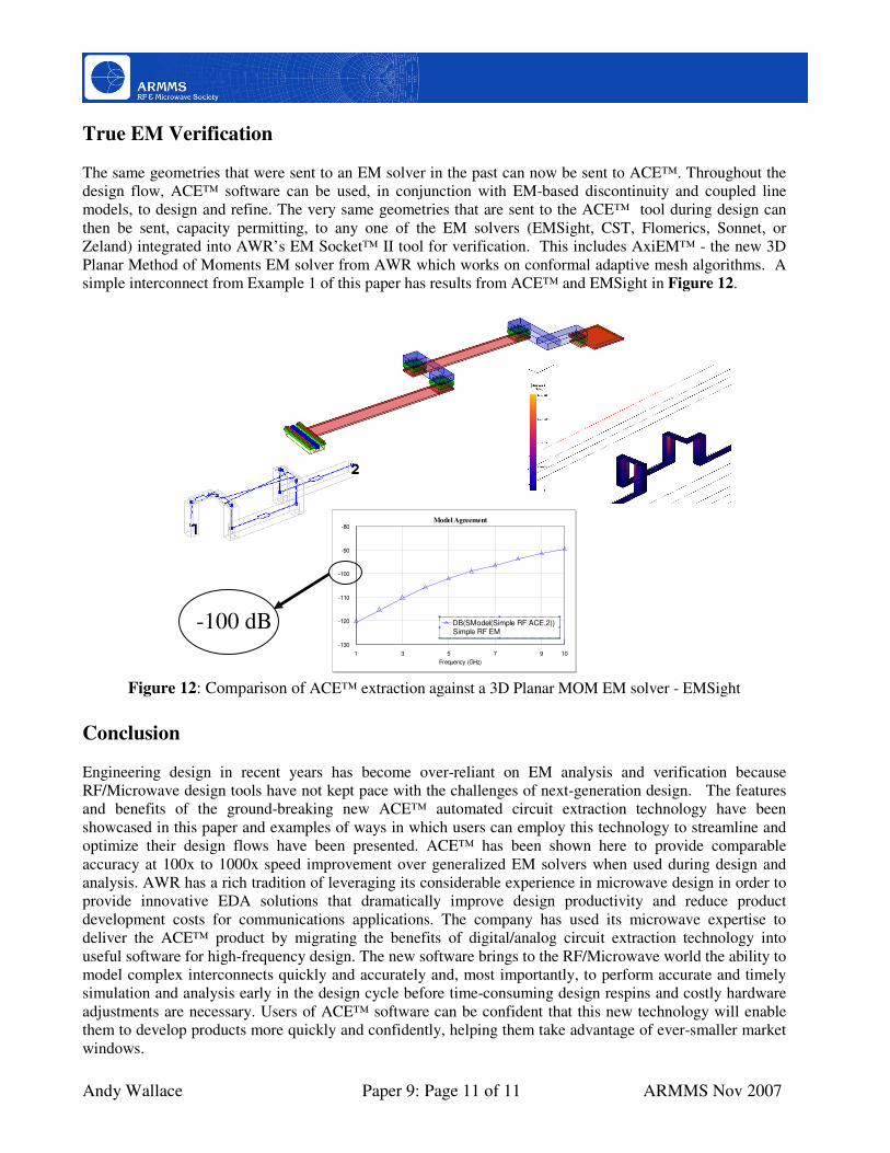
True EM Verification
The same geometries that were sent to an EM solver in the past can now be sent to ACE™. Throughout the
design flow, ACE™ software can be used, in conjunction with EM-based discontinuity and coupled line
models, to design and refine. The very same geometries that are sent to the ACE™ tool during design can
then be sent, capacity permitting, to any one of the EM solvers (EMSight, CST, Flomerics, Sonnet, or
Zeland) integrated into AWR’s EM Socket™ II tool for verification. This includes AxiEM™ - the new 3D
Planar Method of Moments EM solver from AWR which works on conformal adaptive mesh algorithms. A
simple interconnect from Example 1 of this paper has results from ACE™ and EMSight in Figure 12.
Figure 12: Comparison of ACE™ extraction against a 3D Planar MOM EM solver - EMSight
Conclusion
Engineering design in recent years has become over-reliant on EM analysis and verification because
RF/Microwave design tools have not kept pace with the challenges of next-generation design. The features
and benefits of the ground-breaking new ACE™ automated circuit extraction technology have been
showcased in this paper and examples of ways in which users can employ this technology to streamline and
optimize their design flows have been presented. ACE™ has been shown here to provide comparable
accuracy at 100x to 1000x speed improvement over generalized EM solvers when used during design and
analysis. AWR has a rich tradition of leveraging its considerable experience in microwave design in order to
provide innovative EDA solutions that dramatically improve design productivity and reduce product
development costs for communications applications. The company has used its microwave expertise to
deliver the ACE™ product by migrating the benefits of digital/analog circuit extraction technology into
useful software for high-frequency design. The new software brings to the RF/Microwave world the ability to
model complex interconnects quickly and accurately and, most importantly, to perform accurate and timely
simulation and analysis early in the design cycle before time-consuming design respins and costly hardware
adjustments are necessary. Users of ACE™ software can be confident that this new technology will enable
them to develop products more quickly and confidently, helping them take advantage of ever-smaller market
windows.
1 3 5 7 9 10
Frequency (GHz)
Model Agreement
-130
-120
-110
-100
-90
-80
DB(SModel(Simple RF ACE,2))Simple RF EM
-100 dB