acer aspire 7560 service guide
TRANSCRIPT

i
Aspire 7560/7560G
SERVICE GUIDE

ii
Revision HistoryRefer to the following table for the updates made to this service guide.
Service guide files and updates are available on the ACER/CSD Website. For more information, go to http://csd.acer.com.tw. The information in this guide is subject to change without notice.
CopyrightCopyright © 2011 by Acer Incorporated. All rights reserved. No part of this publication may be reproduced, transmitted, transcribed, stored in a retrieval system, or translated into any language or computer language, in any form or by any means, electronic, mechanical, magnetic, optical, chemical, manual or otherwise, without the prior written permission of Acer Incorporated.
DisclaimerThe information in this guide is subject to change without notice.
There are no representations or warranties, either expressed or implied, with respect to the contents hereof and specifically disclaims any warranties of merchantability or fitness for any particular purpose. The software described in this manual is sold or licensed "as is". Should the programs prove defective following their purchase, the buyer (not the manufacturer, distributor, or its dealer) assumes the entire cost of all necessary servicing, repair, and any incidental or consequential damages resulting from any defect in the software.
Date Chapter Updates

iii
ConventionsThe following conventions are used in this manual:
WARNING:!Indicates a potential for personal injury.
CAUTION:!Indicates a potential loss of data or damage to equipment.
IMPORTANT:?Indicates information that is important to know for the proper completion of a procedure, choice of an option, or completing a task.
NOTE:NOTE:Follow local regulations for battery and circuit board disposal. Batteries and Circuit Boards >10 cm² have been highlighted with a yellow rectangle.
The following typographical conventions are used in this document:
Book titles, directory names, file names, path names, and program/process names are shown in italics.
Example:
the DRS5 User's Guide
/usr/local/bin/fd
the /TPH15spool_M program
Computer output (text that represents information displayed on a computer screen, such as menus, prompts, responses to input, and error messages) are shown in constant width.
Example:
[01] The server has been stopped
User input (text that represents information entered by a computer user, such as command names, option letters, and words) are shown in constant width bold.
Variables contained within user input are shown in angle brackets (< >).
Example:
At the prompt, type run <file name> -m
Keyboard keys are shown in bold italics.
Example:
After entering data, press Enter.

iv
General Information 0
This service guide provides all technical information relating to the basic configuration for Acer global product offering. To better fit local market requirements and enhance product competitiveness, your regional office may have decided to extend the functionality of a machine (such as add-on cards, modems, or extra memory capabilities). These localized features are not covered in this generic service guide. In such cases, contact your regional offices or the responsible personnel/channel to provide further technical details.
When ordering FRU parts:
Check the most up-to-date information available on your regional Web or channel. If, for whatever reason, a part number change is made, it may not be noted in this printed service guide.
Acer-authorized Service Providers:
Your Acer office may have a different part number code than those given in the FRU list in this service guide. The list provided by your regional Acer office must be used to order FRU parts for repair and service of customer machines.

v
CHAPTER 1Hardware Specifications
Features . . . . . . . . . . . . . . . . . . . . . . . . . . . . . . . . . . . . . . . . . . . . 1-5Operating System. . . . . . . . . . . . . . . . . . . . . . . . . . . . . . . . . . 1-5Platform . . . . . . . . . . . . . . . . . . . . . . . . . . . . . . . . . . . . . . . . . 1-5System Memory . . . . . . . . . . . . . . . . . . . . . . . . . . . . . . . . . . . 1-5Display. . . . . . . . . . . . . . . . . . . . . . . . . . . . . . . . . . . . . . . . . . . 1-5Graphics . . . . . . . . . . . . . . . . . . . . . . . . . . . . . . . . . . . . . . . . . 1-6Audio Subsystem . . . . . . . . . . . . . . . . . . . . . . . . . . . . . . . . . . 1-7Storage Subsystem . . . . . . . . . . . . . . . . . . . . . . . . . . . . . . . . . 1-7Optical Media Drive . . . . . . . . . . . . . . . . . . . . . . . . . . . . . . . . 1-7Communication . . . . . . . . . . . . . . . . . . . . . . . . . . . . . . . . . . . 1-7Privacy Control . . . . . . . . . . . . . . . . . . . . . . . . . . . . . . . . . . . . 1-8Dimensions and Weight. . . . . . . . . . . . . . . . . . . . . . . . . . . . . 1-8Power Adapter and Battery. . . . . . . . . . . . . . . . . . . . . . . . . . 1-8Special Keys and Controls . . . . . . . . . . . . . . . . . . . . . . . . . . . 1-8I/O Ports. . . . . . . . . . . . . . . . . . . . . . . . . . . . . . . . . . . . . . . . . . 1-9Environment . . . . . . . . . . . . . . . . . . . . . . . . . . . . . . . . . . . . . . 1-9Optional Items . . . . . . . . . . . . . . . . . . . . . . . . . . . . . . . . . . . . 1-9Warranty . . . . . . . . . . . . . . . . . . . . . . . . . . . . . . . . . . . . . . . . . 1-9Software . . . . . . . . . . . . . . . . . . . . . . . . . . . . . . . . . . . . . . . . . 1-10
Notebook Tour. . . . . . . . . . . . . . . . . . . . . . . . . . . . . . . . . . . . . . . 1-11Top View. . . . . . . . . . . . . . . . . . . . . . . . . . . . . . . . . . . . . . . . . 1-11Closed Front View . . . . . . . . . . . . . . . . . . . . . . . . . . . . . . . . . 1-13Rear View . . . . . . . . . . . . . . . . . . . . . . . . . . . . . . . . . . . . . . . . 1-14Left View. . . . . . . . . . . . . . . . . . . . . . . . . . . . . . . . . . . . . . . . . 1-15Right View . . . . . . . . . . . . . . . . . . . . . . . . . . . . . . . . . . . . . . . 1-17Base View . . . . . . . . . . . . . . . . . . . . . . . . . . . . . . . . . . . . . . . . 1-18Touchpad Basics . . . . . . . . . . . . . . . . . . . . . . . . . . . . . . . . . . . 1-20Using the Keyboard . . . . . . . . . . . . . . . . . . . . . . . . . . . . . . . . 1-21Windows Keys. . . . . . . . . . . . . . . . . . . . . . . . . . . . . . . . . . . . . 1-22Hotkeys . . . . . . . . . . . . . . . . . . . . . . . . . . . . . . . . . . . . . . . . . . 1-23
System Block Diagram . . . . . . . . . . . . . . . . . . . . . . . . . . . . . . . . . 1-25Specification Tables . . . . . . . . . . . . . . . . . . . . . . . . . . . . . . . . . . . 1-26
Computer specifications . . . . . . . . . . . . . . . . . . . . . . . . . . . . . 1-26System Board Major Chips . . . . . . . . . . . . . . . . . . . . . . . . . . . 1-27Processor. . . . . . . . . . . . . . . . . . . . . . . . . . . . . . . . . . . . . . . . . 1-27Processor Specifications . . . . . . . . . . . . . . . . . . . . . . . . . . . . . 1-27CPU Fan True Value Table (Tj=100). . . . . . . . . . . . . . . . . . . . 1-28System Memory. . . . . . . . . . . . . . . . . . . . . . . . . . . . . . . . . . . . 1-28Memory Combinations. . . . . . . . . . . . . . . . . . . . . . . . . . . . . . . 1-29Video Interface. . . . . . . . . . . . . . . . . . . . . . . . . . . . . . . . . . . . . 1-29BIOS . . . . . . . . . . . . . . . . . . . . . . . . . . . . . . . . . . . . . . . . . . . . 1-30LAN Interface. . . . . . . . . . . . . . . . . . . . . . . . . . . . . . . . . . . . . . 1-30Keyboard . . . . . . . . . . . . . . . . . . . . . . . . . . . . . . . . . . . . . . . . . 1-31Hard Disk Drive (AVL components). . . . . . . . . . . . . . . . . . . . . 1-31

vi
Super-Multi Drive . . . . . . . . . . . . . . . . . . . . . . . . . . . . . . . . . . . 1-34BD Drive . . . . . . . . . . . . . . . . . . . . . . . . . . . . . . . . . . . . . . . . . 1-35LED 17.3”. . . . . . . . . . . . . . . . . . . . . . . . . . . . . . . . . . . . . . . . . 1-36Display Supported Resolution (LCD). . . . . . . . . . . . . . . . . . . . 1-37Graphics Controller . . . . . . . . . . . . . . . . . . . . . . . . . . . . . . . . . 1-37Display Supported Resolution (GPU) . . . . . . . . . . . . . . . . . . . 1-37Bluetooth Interface. . . . . . . . . . . . . . . . . . . . . . . . . . . . . . . . . . 1-38Bluetooth Module. . . . . . . . . . . . . . . . . . . . . . . . . . . . . . . . . . . 1-38Camera . . . . . . . . . . . . . . . . . . . . . . . . . . . . . . . . . . . . . . . . . . 1-38Mini Card . . . . . . . . . . . . . . . . . . . . . . . . . . . . . . . . . . . . . . . . . 1-38Audio Codec and Amplifier . . . . . . . . . . . . . . . . . . . . . . . . . . . 1-39Audio Interface. . . . . . . . . . . . . . . . . . . . . . . . . . . . . . . . . . . . . 1-39Wireless Module 802.11b/g/n . . . . . . . . . . . . . . . . . . . . . . . . . 1-40Battery . . . . . . . . . . . . . . . . . . . . . . . . . . . . . . . . . . . . . . . . . . . 1-40VRAM . . . . . . . . . . . . . . . . . . . . . . . . . . . . . . . . . . . . . . . . . . . 1-40USB Port . . . . . . . . . . . . . . . . . . . . . . . . . . . . . . . . . . . . . . . . . 1-40HDMI Port . . . . . . . . . . . . . . . . . . . . . . . . . . . . . . . . . . . . . . . . 1-41AC Adapter . . . . . . . . . . . . . . . . . . . . . . . . . . . . . . . . . . . . . . . 1-41System Power Management . . . . . . . . . . . . . . . . . . . . . . . . . . 1-41Card Reader . . . . . . . . . . . . . . . . . . . . . . . . . . . . . . . . . . . . . . 1-42System LED Indicator . . . . . . . . . . . . . . . . . . . . . . . . . . . . . . . 1-42System DMA Specification . . . . . . . . . . . . . . . . . . . . . . . . . . . 1-43System Interrupt Specification . . . . . . . . . . . . . . . . . . . . . . . . . 1-44System IO Address Map . . . . . . . . . . . . . . . . . . . . . . . . . . . . . 1-45System I/O Address Specifications . . . . . . . . . . . . . . . . . . . . . 1-46
CHAPTER 2System Utilities
BIOS Setup Utility. . . . . . . . . . . . . . . . . . . . . . . . . . . . . . . . . . . . . 2-3Navigating the BIOS Utility . . . . . . . . . . . . . . . . . . . . . . . . . . 2-3
BIOS . . . . . . . . . . . . . . . . . . . . . . . . . . . . . . . . . . . . . . . . . . . . . . . 2-4Information. . . . . . . . . . . . . . . . . . . . . . . . . . . . . . . . . . . . . . . 2-4Main . . . . . . . . . . . . . . . . . . . . . . . . . . . . . . . . . . . . . . . . . . . . 2-6Security . . . . . . . . . . . . . . . . . . . . . . . . . . . . . . . . . . . . . . . . . . 2-8Boot. . . . . . . . . . . . . . . . . . . . . . . . . . . . . . . . . . . . . . . . . . . . . 2-13Exit. . . . . . . . . . . . . . . . . . . . . . . . . . . . . . . . . . . . . . . . . . . . . . 2-14
BIOS Flash Utilities . . . . . . . . . . . . . . . . . . . . . . . . . . . . . . . . . . . . 2-15DOS Flash Utility . . . . . . . . . . . . . . . . . . . . . . . . . . . . . . . . . . . 2-16WinFlash Utility . . . . . . . . . . . . . . . . . . . . . . . . . . . . . . . . . . . 2-18
HDD/BIOS Password Utilities . . . . . . . . . . . . . . . . . . . . . . . . . . . . 2-21Clearing HDD Passwords . . . . . . . . . . . . . . . . . . . . . . . . . . . . 2-21Clearing BIOS Passwords . . . . . . . . . . . . . . . . . . . . . . . . . . . . 2-23
Miscellaneous Tools . . . . . . . . . . . . . . . . . . . . . . . . . . . . . . . . . . . 2-25Using Boot Sequence Selector . . . . . . . . . . . . . . . . . . . . . . . . 2-25Using Boot Manager . . . . . . . . . . . . . . . . . . . . . . . . . . . . . . . 2-26Using DMITools. . . . . . . . . . . . . . . . . . . . . . . . . . . . . . . . . . . . 2-27Using LAN MAC EEPROM Utility . . . . . . . . . . . . . . . . . . . . . . 2-29

vii
CHAPTER 3Machine Maintenance Procedures
Introduction . . . . . . . . . . . . . . . . . . . . . . . . . . . . . . . . . . . . . . . . . 3-5General Information . . . . . . . . . . . . . . . . . . . . . . . . . . . . . . . . . . 3-5Recommended Equipment . . . . . . . . . . . . . . . . . . . . . . . . . . . . . 3-5Maintenance Flowchart. . . . . . . . . . . . . . . . . . . . . . . . . . . . . . . . 3-6Getting Started . . . . . . . . . . . . . . . . . . . . . . . . . . . . . . . . . . . . . . 3-7
Dummy Card Removal . . . . . . . . . . . . . . . . . . . . . . . . . . . . . . 3-8Dummy Card Installation . . . . . . . . . . . . . . . . . . . . . . . . . . . . 3-8Battery Removal . . . . . . . . . . . . . . . . . . . . . . . . . . . . . . . . . . . 3-9Battery Installation. . . . . . . . . . . . . . . . . . . . . . . . . . . . . . . . . 3-9ODD Module Removal . . . . . . . . . . . . . . . . . . . . . . . . . . . . . . 3-11ODD Module Installation . . . . . . . . . . . . . . . . . . . . . . . . . . . . 3-13Logic Door Removal . . . . . . . . . . . . . . . . . . . . . . . . . . . . . . . . 3-14Logic Door Installation. . . . . . . . . . . . . . . . . . . . . . . . . . . . . . 3-14Main and Secondary HDD Module Removal . . . . . . . . . . . . 3-15Main and Secondary HDD Module Installation . . . . . . . . . . 3-17Main and Secondary HDD Module Carrier Removal . . . . . . 3-18Main and Secondary HDD Module Carrier Installation . . . . 3-19WLAN Module Removal. . . . . . . . . . . . . . . . . . . . . . . . . . . . . 3-20WLAN Module Installation . . . . . . . . . . . . . . . . . . . . . . . . . . 3-21DIMM Module Removal . . . . . . . . . . . . . . . . . . . . . . . . . . . . . 3-22DIMM Module Installation. . . . . . . . . . . . . . . . . . . . . . . . . . . 3-23Keyboard Removal . . . . . . . . . . . . . . . . . . . . . . . . . . . . . . . . . 3-24Keyboard Installation. . . . . . . . . . . . . . . . . . . . . . . . . . . . . . . 3-26Upper Cover Removal . . . . . . . . . . . . . . . . . . . . . . . . . . . . . . 3-27Upper Cover Installation . . . . . . . . . . . . . . . . . . . . . . . . . . . . 3-30Touchpad FFC Removal . . . . . . . . . . . . . . . . . . . . . . . . . . . . . 3-32Touchpad FFC Installation . . . . . . . . . . . . . . . . . . . . . . . . . . . 3-33Power Board Removal . . . . . . . . . . . . . . . . . . . . . . . . . . . . . . 3-34Power Board Installation . . . . . . . . . . . . . . . . . . . . . . . . . . . . 3-35RJ45 Module Removal . . . . . . . . . . . . . . . . . . . . . . . . . . . . . . 3-36RJ45 Module Installation . . . . . . . . . . . . . . . . . . . . . . . . . . . . 3-37USB Module Removal. . . . . . . . . . . . . . . . . . . . . . . . . . . . . . . 3-38USB Module Installation . . . . . . . . . . . . . . . . . . . . . . . . . . . . 3-39Bluetooth Module Removal. . . . . . . . . . . . . . . . . . . . . . . . . . 3-40Bluetooth Module Installation . . . . . . . . . . . . . . . . . . . . . . . 3-41RTC Battery Removal . . . . . . . . . . . . . . . . . . . . . . . . . . . . . . . 3-42RTC Battery Installation . . . . . . . . . . . . . . . . . . . . . . . . . . . . . 3-42Speaker Module Removal . . . . . . . . . . . . . . . . . . . . . . . . . . . 3-43Speaker Module Installation . . . . . . . . . . . . . . . . . . . . . . . . . 3-44Mainboard Removal. . . . . . . . . . . . . . . . . . . . . . . . . . . . . . . . 3-45Mainboard Installation . . . . . . . . . . . . . . . . . . . . . . . . . . . . . 3-47Thermal Fan Module Removal. . . . . . . . . . . . . . . . . . . . . . . . 3-48Thermal Fan Module Installation . . . . . . . . . . . . . . . . . . . . . 3-49Thermal Module Removal . . . . . . . . . . . . . . . . . . . . . . . . . . . 3-50

viii
Thermal Module Installation . . . . . . . . . . . . . . . . . . . . . . . . . 3-51CPU Removal. . . . . . . . . . . . . . . . . . . . . . . . . . . . . . . . . . . . . . 3-52CPU Installation . . . . . . . . . . . . . . . . . . . . . . . . . . . . . . . . . . . 3-52PCH Heatsink Removal . . . . . . . . . . . . . . . . . . . . . . . . . . . . . . 3-53PCH Heatsink Installation. . . . . . . . . . . . . . . . . . . . . . . . . . . . 3-53LCD Module Removal. . . . . . . . . . . . . . . . . . . . . . . . . . . . . . . 3-54LCD Module Installation . . . . . . . . . . . . . . . . . . . . . . . . . . . . 3-56DC-IN Cable Removal . . . . . . . . . . . . . . . . . . . . . . . . . . . . . . . 3-57DC-IN Cable Installation. . . . . . . . . . . . . . . . . . . . . . . . . . . . . 3-58LCD Bezel Removal. . . . . . . . . . . . . . . . . . . . . . . . . . . . . . . . . 3-59LCD Bezel Installation . . . . . . . . . . . . . . . . . . . . . . . . . . . . . . 3-60CCD Module Removal . . . . . . . . . . . . . . . . . . . . . . . . . . . . . . 3-63CCD Module Installation . . . . . . . . . . . . . . . . . . . . . . . . . . . . 3-63LCD Panel Removal. . . . . . . . . . . . . . . . . . . . . . . . . . . . . . . . . 3-64LCD Panel Installation . . . . . . . . . . . . . . . . . . . . . . . . . . . . . . 3-65LCD Brackets Removal . . . . . . . . . . . . . . . . . . . . . . . . . . . . . . 3-67LCD Brackets Installation . . . . . . . . . . . . . . . . . . . . . . . . . . . . 3-67LVDS Cable Removal . . . . . . . . . . . . . . . . . . . . . . . . . . . . . . . 3-68LVDS Cable Installation . . . . . . . . . . . . . . . . . . . . . . . . . . . . . 3-69Microphone Module Removal . . . . . . . . . . . . . . . . . . . . . . . . 3-70Microphone Module Installation. . . . . . . . . . . . . . . . . . . . . . 3-70WLAN Antenna Removal . . . . . . . . . . . . . . . . . . . . . . . . . . . . 3-71WLAN Antenna Installation. . . . . . . . . . . . . . . . . . . . . . . . . . 3-71
CHAPTER 4Troubleshooting
Introduction . . . . . . . . . . . . . . . . . . . . . . . . . . . . . . . . . . . . . . . . . 4-3General Information . . . . . . . . . . . . . . . . . . . . . . . . . . . . . . . . . . 4-3
Power On Issues . . . . . . . . . . . . . . . . . . . . . . . . . . . . . . . . . . . 4-4No Display Issues. . . . . . . . . . . . . . . . . . . . . . . . . . . . . . . . . . . 4-5LCD Failure . . . . . . . . . . . . . . . . . . . . . . . . . . . . . . . . . . . . . . . 4-7Keyboard Failure . . . . . . . . . . . . . . . . . . . . . . . . . . . . . . . . . . 4-8Touchpad Failure . . . . . . . . . . . . . . . . . . . . . . . . . . . . . . . . . . 4-9Internal Speaker Failure. . . . . . . . . . . . . . . . . . . . . . . . . . . . . 4-10Microphone Failure . . . . . . . . . . . . . . . . . . . . . . . . . . . . . . . . 4-12USB Failure . . . . . . . . . . . . . . . . . . . . . . . . . . . . . . . . . . . . . . . 4-13Wireless Function Failure . . . . . . . . . . . . . . . . . . . . . . . . . . . . 4-14Bluetooth Failure . . . . . . . . . . . . . . . . . . . . . . . . . . . . . . . . . . 4-15Card Reader Failure . . . . . . . . . . . . . . . . . . . . . . . . . . . . . . . . 4-16Thermal Unit Failure . . . . . . . . . . . . . . . . . . . . . . . . . . . . . . . 4-17Case Failure. . . . . . . . . . . . . . . . . . . . . . . . . . . . . . . . . . . . . . . 4-18Other Functions Failure . . . . . . . . . . . . . . . . . . . . . . . . . . . . . 4-19ODD Failure . . . . . . . . . . . . . . . . . . . . . . . . . . . . . . . . . . . . . . 4-20
Intermittent Problems . . . . . . . . . . . . . . . . . . . . . . . . . . . . . . . . . 4-25Undetermined Problems . . . . . . . . . . . . . . . . . . . . . . . . . . . . . . . 4-25Post Codes . . . . . . . . . . . . . . . . . . . . . . . . . . . . . . . . . . . . . . . . . . 4-26

ix
CHAPTER 5Jumper and Connector Locations
Mainboard Top . . . . . . . . . . . . . . . . . . . . . . . . . . . . . . . . . . . . . . 5-3Mainboard Bottom . . . . . . . . . . . . . . . . . . . . . . . . . . . . . . . . . . . 5-4Clearing Password and BIOS Recovery . . . . . . . . . . . . . . . . . . . . 5-5
Clearing Password . . . . . . . . . . . . . . . . . . . . . . . . . . . . . . . . . 5-5BIOS Recovery by Crisis Disk. . . . . . . . . . . . . . . . . . . . . . . . . . 5-6
CHAPTER 6Field Replaceable Unit List
Exploded Diagrams . . . . . . . . . . . . . . . . . . . . . . . . . . . . . . . . . . . 6-4Main Assembly . . . . . . . . . . . . . . . . . . . . . . . . . . . . . . . . . . . . 6-4LCD Assembly . . . . . . . . . . . . . . . . . . . . . . . . . . . . . . . . . . . . . 6-6Lower Cover . . . . . . . . . . . . . . . . . . . . . . . . . . . . . . . . . . . . . . 6-8
FRU List . . . . . . . . . . . . . . . . . . . . . . . . . . . . . . . . . . . . . . . . . . . . . 6-9Screw List . . . . . . . . . . . . . . . . . . . . . . . . . . . . . . . . . . . . . . . . . . . 6-20
CHAPTER 7Model Definition and Configuration
Aspire 7560. . . . . . . . . . . . . . . . . . . . . . . . . . . . . . . . . . . . . . . . . . 7-3Aspire 7560G . . . . . . . . . . . . . . . . . . . . . . . . . . . . . . . . . . . . . . . . 7-13
CHAPTER 8Test Compatible Components
Microsoft® Windows® 7 Environment Test. . . . . . . . . . . . . . . . 8-4Aspire 7560/7560G . . . . . . . . . . . . . . . . . . . . . . . . . . . . . . . . . 8-4
CHAPTER 9Online Support Information
Information . . . . . . . . . . . . . . . . . . . . . . . . . . . . . . . . . . . . . . . . . 9-3

x

CHAPTER 1
Hardware Specifications

1-2
Features . . . . . . . . . . . . . . . . . . . . . . . . . . . . . . . . . . . . . . . . . . . . 1-5Operating System. . . . . . . . . . . . . . . . . . . . . . . . . . . . . . . . . . 1-5Platform . . . . . . . . . . . . . . . . . . . . . . . . . . . . . . . . . . . . . . . . . 1-5System Memory . . . . . . . . . . . . . . . . . . . . . . . . . . . . . . . . . . . 1-5Display. . . . . . . . . . . . . . . . . . . . . . . . . . . . . . . . . . . . . . . . . . . 1-5Graphics . . . . . . . . . . . . . . . . . . . . . . . . . . . . . . . . . . . . . . . . . 1-6Audio Subsystem . . . . . . . . . . . . . . . . . . . . . . . . . . . . . . . . . . 1-7Storage Subsystem . . . . . . . . . . . . . . . . . . . . . . . . . . . . . . . . . 1-7Optical Media Drive . . . . . . . . . . . . . . . . . . . . . . . . . . . . . . . . 1-7Communication . . . . . . . . . . . . . . . . . . . . . . . . . . . . . . . . . . . 1-7Privacy Control . . . . . . . . . . . . . . . . . . . . . . . . . . . . . . . . . . . . 1-8Dimensions and Weight. . . . . . . . . . . . . . . . . . . . . . . . . . . . . 1-8Power Adapter and Battery. . . . . . . . . . . . . . . . . . . . . . . . . . 1-8Special Keys and Controls . . . . . . . . . . . . . . . . . . . . . . . . . . . 1-8I/O Ports. . . . . . . . . . . . . . . . . . . . . . . . . . . . . . . . . . . . . . . . . . 1-9Environment . . . . . . . . . . . . . . . . . . . . . . . . . . . . . . . . . . . . . . 1-9Optional Items . . . . . . . . . . . . . . . . . . . . . . . . . . . . . . . . . . . . 1-9Warranty . . . . . . . . . . . . . . . . . . . . . . . . . . . . . . . . . . . . . . . . . 1-9Software . . . . . . . . . . . . . . . . . . . . . . . . . . . . . . . . . . . . . . . . . 1-10
Notebook Tour. . . . . . . . . . . . . . . . . . . . . . . . . . . . . . . . . . . . . . . 1-11Top View. . . . . . . . . . . . . . . . . . . . . . . . . . . . . . . . . . . . . . . . . 1-11Closed Front View . . . . . . . . . . . . . . . . . . . . . . . . . . . . . . . . . 1-13Rear View . . . . . . . . . . . . . . . . . . . . . . . . . . . . . . . . . . . . . . . . 1-14Left View. . . . . . . . . . . . . . . . . . . . . . . . . . . . . . . . . . . . . . . . . 1-15Right View . . . . . . . . . . . . . . . . . . . . . . . . . . . . . . . . . . . . . . . 1-17Base View . . . . . . . . . . . . . . . . . . . . . . . . . . . . . . . . . . . . . . . . 1-18Touchpad Basics . . . . . . . . . . . . . . . . . . . . . . . . . . . . . . . . . . . 1-20Using the Keyboard . . . . . . . . . . . . . . . . . . . . . . . . . . . . . . . . 1-21Windows Keys. . . . . . . . . . . . . . . . . . . . . . . . . . . . . . . . . . . . . 1-22Hotkeys . . . . . . . . . . . . . . . . . . . . . . . . . . . . . . . . . . . . . . . . . . 1-23
System Block Diagram . . . . . . . . . . . . . . . . . . . . . . . . . . . . . . . . . 1-25Specification Tables . . . . . . . . . . . . . . . . . . . . . . . . . . . . . . . . . . . 1-26
Computer specifications . . . . . . . . . . . . . . . . . . . . . . . . . . . . . 1-26System Board Major Chips . . . . . . . . . . . . . . . . . . . . . . . . . . . 1-27Processor. . . . . . . . . . . . . . . . . . . . . . . . . . . . . . . . . . . . . . . . . 1-27Processor Specifications . . . . . . . . . . . . . . . . . . . . . . . . . . . . . 1-27CPU Fan True Value Table (Tj=100). . . . . . . . . . . . . . . . . . . . 1-28System Memory. . . . . . . . . . . . . . . . . . . . . . . . . . . . . . . . . . . . 1-28Memory Combinations. . . . . . . . . . . . . . . . . . . . . . . . . . . . . . . 1-29Video Interface. . . . . . . . . . . . . . . . . . . . . . . . . . . . . . . . . . . . . 1-29BIOS . . . . . . . . . . . . . . . . . . . . . . . . . . . . . . . . . . . . . . . . . . . . 1-30LAN Interface. . . . . . . . . . . . . . . . . . . . . . . . . . . . . . . . . . . . . . 1-30Keyboard . . . . . . . . . . . . . . . . . . . . . . . . . . . . . . . . . . . . . . . . . 1-31Hard Disk Drive (AVL components). . . . . . . . . . . . . . . . . . . . . 1-31Super-Multi Drive . . . . . . . . . . . . . . . . . . . . . . . . . . . . . . . . . . . 1-34BD Drive . . . . . . . . . . . . . . . . . . . . . . . . . . . . . . . . . . . . . . . . . 1-35

1-3
LED 17.3”. . . . . . . . . . . . . . . . . . . . . . . . . . . . . . . . . . . . . . . . . 1-36Display Supported Resolution (LCD). . . . . . . . . . . . . . . . . . . . 1-37Graphics Controller . . . . . . . . . . . . . . . . . . . . . . . . . . . . . . . . . 1-37Display Supported Resolution (GPU) . . . . . . . . . . . . . . . . . . . 1-37Bluetooth Interface. . . . . . . . . . . . . . . . . . . . . . . . . . . . . . . . . . 1-38Bluetooth Module. . . . . . . . . . . . . . . . . . . . . . . . . . . . . . . . . . . 1-38Camera . . . . . . . . . . . . . . . . . . . . . . . . . . . . . . . . . . . . . . . . . . 1-38Mini Card . . . . . . . . . . . . . . . . . . . . . . . . . . . . . . . . . . . . . . . . . 1-38Audio Codec and Amplifier . . . . . . . . . . . . . . . . . . . . . . . . . . . 1-39Audio Interface. . . . . . . . . . . . . . . . . . . . . . . . . . . . . . . . . . . . . 1-39Wireless Module 802.11b/g/n . . . . . . . . . . . . . . . . . . . . . . . . . 1-40Battery . . . . . . . . . . . . . . . . . . . . . . . . . . . . . . . . . . . . . . . . . . . 1-40VRAM . . . . . . . . . . . . . . . . . . . . . . . . . . . . . . . . . . . . . . . . . . . 1-40USB Port . . . . . . . . . . . . . . . . . . . . . . . . . . . . . . . . . . . . . . . . . 1-40HDMI Port . . . . . . . . . . . . . . . . . . . . . . . . . . . . . . . . . . . . . . . . 1-41AC Adapter . . . . . . . . . . . . . . . . . . . . . . . . . . . . . . . . . . . . . . . 1-41System Power Management . . . . . . . . . . . . . . . . . . . . . . . . . . 1-41Card Reader . . . . . . . . . . . . . . . . . . . . . . . . . . . . . . . . . . . . . . 1-42System LED Indicator . . . . . . . . . . . . . . . . . . . . . . . . . . . . . . . 1-42System DMA Specification . . . . . . . . . . . . . . . . . . . . . . . . . . . 1-43System Interrupt Specification . . . . . . . . . . . . . . . . . . . . . . . . . 1-44System IO Address Map . . . . . . . . . . . . . . . . . . . . . . . . . . . . . 1-45System I/O Address Specifications . . . . . . . . . . . . . . . . . . . . . 1-46

1-4

Hardware Specifications and Configurations 1-5
Hardware Specifications and Configurations
Features 0
The following is a summary of the computer’s many features:
Operating System 0
Genuine Windows® 7 Home Premium 64-bit
Genuine Windows® 7 Home Basic 64-bit
Platform 0
AMD A-Series quad-core processor A8-3510MX/A8-3530MX (4 MB L2 cache, 1.80/1.90 GHz with Turbo CORE Technology up to 2.50/2.60 GHz, DDR3 1600 MHz, 45 W), A8-3500M (4 MB L2 cache, 1.50 GHz with Turbo CORE Technology up to 2.40 GHz, DDR3 1333 MHz, 35 W)
AMD A-Series quad-core processor A6-3410MX (4 MB L2 cache, 1.60 GHz with Turbo CORE Technology up to 2.30 GHz, DDR3 1600 MHz, 45 W), A6-3400M (4 MB L2 cache, 1.40 GHz with Turbo CORE Technology up to 2.30 GHz, DDR3 1333 MHz, 35 W)
AMD A-Series dual-core processor A4-3310MX (2 MB L2 cache, 2.10 GHz with Turbo CORE Technology up to 2.50 GHz, DDR3 1333 MHz, 45 W), A4-3300M (2 MB L2 cache, 1.90 GHz with Turbo CORE Technology up to 2.50 GHz, DDR3 1333 MHz, 35 W)
AMD E-Series dual-core processor E2-3000M (1 MB L2 cache, 1.80 GHz with Turbo CORE Technology up to 2.40 GHz, DDR3 1333 MHz, 35 W)
AMD A70M Fusion™ Controller Hub
System Memory 0
Dual-channel DDR3 SDRAM support:
Up to 4 GB of DDR3 system memory, upgradable to 8 GB using two soDIMM modules
Display 0
17.3" HD+ 1600 x 900 resolution, high-brightness (220-nit) Acer CineCrystal™ LED-backlit TFT LCD
Mercury-free, environment-friendly
8 ms response time
60% color gamut
16:9 aspect ratio

1-6 Hardware Specifications and Configurations
Graphics 0
Dual independent display support
16.7 million colors
MPEG-2/DVD decoding
VC-1 and H.264 (AVC) decoding
HDMI® (High-Definition Multimedia Interface) with HDCP (High-bandwidth Digital Content Protection) support
Aspire 7560 0
AMD Radeon™ HD 6620M Graphics with 256 MB of dedicated system memory,
supporting Unified Video Decoder 3 (UVD3), OpenCL® 1.1, Open GL 3.1, OpenEXR
High Dynamic-Range (HDR) technology, Shader Model 5.0, Microsoft® DirectX® 11
AMD Radeon™ HD 6520M Graphics with 256 MB of dedicated system memory,
supporting Unified Video Decoder 3 (UVD3), OpenCL® 1.1, Open GL 3.1, OpenEXR
High Dynamic-Range (HDR) technology, Shader Model 5.0, Microsoft® DirectX® 11
AMD Radeon™ HD 6480M Graphics with 256 MB of dedicated system memory,
supporting Unified Video Decoder 3 (UVD3), OpenCL® 1.1, Open GL 3.1, OpenEXR
High Dynamic-Range (HDR) technology, Shader Model 5.0, Microsoft® DirectX® 11
AMD Radeon™ HD 6380M Graphics with 256 MB of dedicated system memory,
supporting Unified Video Decoder 3 (UVD3), OpenCL® 1.1, Open GL 3.1, OpenEXR
High Dynamic-Range (HDR) technology, Shader Model 5.0, Microsoft® DirectX® 11
External resolution / refresh rates:
VGA port up to 2560 x 1600: 85 Hz
HDMI® port up to 1920 x 1080: 60 Hz
MPEG-4 Part 2 DivX® decoding
Aspire 7560G 0
AMD Radeon™ HD 6650M with 2048 MB of dedicated DDR3 VRAM, supporting Unified Video Decoder 3 (UVD 3), OpenEXR High Dynamic-Range (HDR) technology,
Shader Model 5.0, Microsoft® DirectXv 11, OpenGL® 3.1, OpenCL™ 1.1
AMD Radeon™ HD 6470M with 1024 MB of dedicated DDR3 VRAM, supporting Unified Video Decoder 3 (UVD 3), OpenEXR High Dynamic-Range (HDR) technology,
Shader Model 5.0, Microsoft® DirectX® 11, OpenGL® 3.1, OpenCL™ 1.1
External resolution / refresh rates:
VGA port up to 2048 x 1536: 85 Hz
HDMI® port up to 1920 x 1080: 60 Hz
MPEG-4 Part 2 DivX® and Xvid decoding
Microsoft® DirectX® Video Acceleration (DXVA) application interface (API)

Hardware Specifications and Configurations 1-7
Audio Subsystem 0
Optimized Dolby® Advanced Audio® v2 audio enhancement, featuring Audio Optimizer, Audio Regulator, Volume Leveler, Volume Maximizer, and Surround Virtualizer (for built-in speakers) technologies
High-definition audio support
Two built-in stereo speakers
MS-Sound compatible
Built-in microphone
Storage Subsystem 0
Hard disk drive
250/320/500/640/750 GB or larger
Multi-in-1 card reader, supporting:
Secure Digital™ (SD) Card, MultiMediaCard™ (MMC), Memory Stick™ (MS),Memory Stick PRO™ (MS PRO), xD-Picture Card™ (xD)
Optical Media Drive 0
4X Blu-ray Disc™ / DVD-Super Multi double-layer drive:
Read: 24X CD-ROM, 24X CD-R, 16X CD-RW, 8X DVD-ROM, 8X DVD-R, 8X DVD+R, 4X DVD-ROM DL, 4X DVD-R DL, 4X DVD+R DL, 4X DVD-RW, 4X DVD+RW, 5X DVD-RAM, 4X BD-ROM, 4X BD-R, 4X BD-RE, 4X BD-ROM DL, 4X BD-R DL, 4X BD-RE DL
Write: 16X CD-R, 10X CD-RW, 8X DVD-R, 8X DVD+R, 4X DVD-RW, 4X DVD+RW, 5X DVD-RAM, 4X DVD+R DL, 4X DVD-R DL
8X DVD-Super Multi double-layer drive:
Read: 24X CD-ROM, 24X CD-R, 24X CD-RW, 8X DVD-ROM, 8X DVD-R, 8X DVD+R, 6X DVD-ROM DL, 4X DVD-R DL, 4X DVD+R DL, 6X DVD-RW, 6X DVD+RW, 5X DVD-RAM
Write: 24X CD-R, 16X CD-RW, 8X DVD-R, 8X DVD+R, 4X DVD-R DL, 4X DVD+R DL, 6X DVD-RW, 8X DVD+RW, 5X DVD-RAM
Communication 0
Webcam
Acer Video Conference, featuring:
Acer Crystal Eye webcam with 1280 x 1024 resolution
WLAN:
Acer InviLink™ Nplify™ 802.11b/g/n Wi-Fi CERTIFIED™
Acer InviLink™ 802.11b/g Wi-Fi CERTIFIED™
Supporting Acer SignalUp™ wireless technology
WPAN:
Bluetooth® 3.0+HS
Bluetooth® 2.0/2.1+EDR
LAN:
Gigabit Ethernet, Wake-on-LAN ready

1-8 Hardware Specifications and Configurations
Privacy Control 0
BIOS user, supervisor, HDD passwords
Kensington lock slot
Dimensions and Weight 0
Dimensions
414.75 (W) x 275 (D) x 34.6 (H) mm (16.59 x 11 x 1.38 inches)
Weight
3.3 kg (7.27 lbs.) with 6-cell battery pack
Power Adapter and Battery 0
ACPI 3.0 CPU power management standard: supports Standby and Hibernation power-saving modes
Battery
48 Wh 4400 mAh 6-cell Li-ion standard battery pack
Battery life: TBC hours
ENERGY STAR®
Power adapter
Aspire 7560 0
3-pin 65 W AC adapter:
95 (W) x 50 (D) x 25.4 (H) mm (3.74 x 1.96 x 1 inches)
216 g (0.47 lbs.) with 180 cm DC cable
Aspire 7560G 0
3-pin 90 W AC adapter:
133 (W) x 59 (D) x 31 (H) mm (5.23 x 2.32 x 1.22 inches)
390 g (0.86 lbs.) with 180 cm DC cable
Special Keys and Controls 0
Keyboard
103-/104-/107-key Acer FineTip keyboard with independent standard numeric keypad, international language support
Touchpad
Multi-gesture touchpad, supporting two-finger scroll, pinch, rotate, flip
Media keys
Media control keys (printed on keyboard): play/pause, stop, previous, next, volume up, volume down

Hardware Specifications and Configurations 1-9
I/O Ports 0
Multi-in-1 card reader (SD™, MMC,MS,MS PRO, xD)
Three USB 2.0 ports
HDMI® port with HDCP support
External display (VGA) port
Headphone/speaker jack, supporting 3.5 mm headset with built-in microphone for Acer smart handhelds
Microphone-in jack
Ethernet (RJ-45) port
DC-in jack for AC adapter
Environment 0
Temperature:
Operating: 5°C to 35°C
Non-operating: -20°C to 65°C
Humidity (non-condensing):
Operating: 20% to 80%
Non-operating: 20% to 80%
Optional Items 0
1/2/4 GB DDR3 soDIMM module
6-cell Li-ion battery pack
External USB 56K modem
Aspire 7560 0
3-pin 65 W AC adapter
Aspire 7560G 0
3-pin 90W AC adapter
Warranty 0
One-year International Travelers Warranty (ITW)

1-10 Hardware Specifications and Configurations
Software 0
Productivity
Acer Backup Manager
Acer ePower Management
Acer eRecovery Management
Adobe® Flash® Player 10.1
Adobe® Reader® 9.1
AUPEO! (US only)
Bing™ Bar
eSobi™
Kobo™ (Canada only)
Microsoft® Office 2010 preloaded (purchase a product key to activate)
Microsoft® Office Starter 2010
New York Times Reader (US only)
NOOK for PC (US only)
Norton™ Online Backup
Security
McAfee® Internet Security Suite Trial
MyWinLocker®
Multimedia
Acer clear.fi
NTI Media Maker™
Gaming
Oberon GameZone (except US, Canada, Hong Kong, Korea)
WildTangent® (US, Canada only)
Communication and ISP
Acer Crystal Eye
Microsoft® Silverlight™
Skype™
Windows Live™ Essentials 2011
Web links and utilities
Acer Accessory Store (Belgium, France, Germany, Italy, Netherlands, Spain, Sweden, UK only)
Acer Identity Card
Acer Registration
Acer Updater
eBay® shortcut 2009 (Canada, France, Germany, Italy, Mexico, Spain, UK, US only)
Netflix shortcut1 (US only)

Hardware Specifications and Configurations 1-11
Notebook Tour 0
Top View 0
Figure 1-1. Top View
Table 1-1. Top View
# Icon Item Description
1 Acer Crystal Eye webcam
Web camera for video communication. (only for certain models)
2 Display screen Also called Liquid-Crystal Display (LCD), displays computer output (Configuration may vary by models).
1
2
3
9
4
5
6
8
7

1-12 Hardware Specifications and Configurations
3 Power button Turns the computer on and off.
4 Keyboard For entering data into your computer.
5 Touchpad Touch-sensitive pointing device which functions like a computer mouse.
6 Click buttons (left and right)
The left and right buttons function like the left and right mouse buttons.
7 Palmrest Comfortable support area for your hands when you use the computer.
8 Speakers Deliver stereo audio output.
9 Microphone Internal microphone for sound recording.
Table 1-1. Top View (Continued)
# Icon Item Description

Hardware Specifications and Configurations 1-13
Closed Front View 0
Figure 1-2. Front View
Table 1-2. Front View
# Icon Item Description
1 Power indicator Indicates the computer's power status.
Battery indicator Indicates the computer's battery status.
Charging: The light shows amber when the battery is charging.
Fully charged: The light shows blue when in AC mode.
HDD indicator Indicates when the hard disk drive is active.
Communication indicator
Indicates the computer’s wireless connectivity device status.
2 Multi-in-1 card reader Accepts Secure Digital (SD), MultiMediaCard (MMC), Memory Stick PRO (MS PRO), xD-Picture Card (xD).
NOTE:Push to remove/install the card. Only one card can operate at any given time.
21

1-14 Hardware Specifications and Configurations
Rear View 0
Figure 1-3. Rear View
Table 1-3. Rear View
# Icon Item Description
1 Battery bay Houses the computer's battery pack.
1

Hardware Specifications and Configurations 1-15
Left View 0
Figure 1-4. Left View
Table 1-4. Left View
# Icon Item Description
1 Kensington lock slot Connects to a Kensington-compatible computer security lock.
NOTE:Wrap the computer security lock cable around an immovable object such as a table or handle of a locked drawer. Insert the lock into the notch and turn the key to secure the lock. Some keyless models are also available.
2 Ventilation slots Enable the computer to stay cool, even after prolonged use.
3 External display (VGA) port
Connects to a display device (e.g., external monitor, LCD projector).
4 HDMI port Supports high-definition digital video connections.
5 USB 2.0 port Connects to USB 2.0 devices (e.g., USB mouse, USB camera).
1 2 3 4 5 6

1-16 Hardware Specifications and Configurations
6 Microphone jack Accepts inputs from external microphones.
Headphones/speaker jack
Connects to audio devices (e.g., speakers, headphones).
NOTE:Supports compatible 3.5 mm headsets with built-in microphone (e.g. Acer smart handheld headsets).
Table 1-4. Left View (Continued)
# Icon Item Description

Hardware Specifications and Configurations 1-17
Right View 0
Figure 1-5. Right View
Table 1-5. Right View
# Icon Item Description
1 USB 2.0 ports Connect to USB 2.0 devices (e.g., USB mouse, USB camera).
2 Optical drive Internal optical drive; accepts CDs, DVDs, or Blu-ray Discs (for certain models only).
3 Optical drive access indicator
Lights up when the optical drive is active.
4 Optical drive eject button
Ejects the optical disc from the drive.
5 Emergency eject hole Ejects the optical drive tray when the computer is turned off.
NOTE:Insert a paper clip to the emergency eject hole to eject the optical drive tray when the computer is off.
6 Ethernet (RJ-45) port Connects to an Ethernet 10/100/1000-based network.
7 DC-in jack Connects to an AC adapter.
1 2 3 4 5 6 7

1-18 Hardware Specifications and Configurations
Base View 0
Figure 1-6. Base View
Figure 1-7. Battery Release Latch/Lock
Table 1-6. Base View
# Icon Item Description
1 Battery bay Houses the computer's battery pack.
2 Battery release latch/ lock
Releases the battery for removal.
Insert a suitable tool into the latch and slide to release.
1
2
3
4 5

Hardware Specifications and Configurations 1-19
4 Memory compartment Houses the computer's main memory.
5 Hard disk bay-Main Houses the computer's hard disk (secured with screws).
6 Hard disk bay-Secondary
Houses the computer's hard disk (secured with screws) (for certain models only).
Table 1-6. Base View (Continued)
# Icon Item Description

1-20 Hardware Specifications and Configurations
Touchpad Basics 0
Figure 1-8. Touchpad
Move a finger across the Touchpad (1) to move the cursor.
Press the left (2) and right (3) buttons located beneath the Touchpad to perform selection and execution functions. These two buttons are the equivalent of the left and right buttons on a mouse. Tapping on the Touchpad is the same as clicking the left button.
Table 1-7. Touchpad
Function Main TouchPad (1) Left Button (2) Right Button (3)
Execute Tap twice (at the same speed as double-clicking a mouse button).
Quickly click twice.
Select Tap once. Click once.
Drag Tap twice (at the same speed as double-clicking a mouse button); rest your finger on the TouchPad on the second tap and drag the cursor.
Click and hold, then use finger on the Touchpad to drag the cursor.
Access context menu
Click once.
NOTE:When using the TouchPad, keep it - and fingers - dry and clean. The TouchPad is sensitive to finger movement; hence, the lighter the touch, the better the response. Tapping too hard will not increase the TouchPad’s responsiveness.
1
2 3

Hardware Specifications and Configurations 1-21
Using the Keyboard 0
Figure 1-9. Keyboard Lock Keys
The keyboard has three lock keys which can be toggled on and off. (Table 1-8)
Table 1-8. Keyboard Lock Keys
Lock key Description
Caps Lock When Caps Lock is on, all alphabetic characters typed are in uppercase.
Num Lock When Num Lock is on, the numeric keypad is in numeric mode. The keys function as a calculator (complete with the arithmetic operators +, -, *, and /).
Scroll Lock <Fn> + <F12>
When Scroll Lock is on, the screen moves one line up or down when the up or down arrow keys are pressed respectively. Scroll Lock does not work with some applications.

1-22 Hardware Specifications and Configurations
Windows Keys 0
The keyboard has two keys that perform Windows-specific functions.
Windows Logo key
Application key
Table 1-9. Windows Keys
Key Description
Windows Logo key
Pressed alone, this key has the same effect as clicking on the Windows Start button; it launches the Start menu. It can also be used with other keys to provide a variety of functions.
Functions supported by Windows XP, Windows Vista, and Windows 7:
: Open or close the Start menu
+ R: Open the Run dialog box
+ M: Minimizes all windows
Shift + + M: Undo minimize all windows
+ F1: Show the help window
+ E: Open Windows Explorer
+ F: Search for a file or folder
+ D: Show the desktop
Ctrl + + F: Search for computers (if you are on a network)
+ L: Lock your computer (if you are connected to a network domain), or switch users (if you're not connected to a network domain)
Ctrl + + Tab: Moves focus from Start menu, to the Quick Launch toolbar, to the system tray (use or to move focus to items on the Quick Launch toolbar and the system tray)
+ Tab: Cycle through programs on the taskbar
+ Break: Display the System Properties dialog box
Functions supported by Windows XP:
+ Break: Show the System Properties dialog box
+ U: Open Ease of Access Center
Application key This key has the same effect as clicking the right mouse button; it opens the application's context menu.

Hardware Specifications and Configurations 1-23
Hotkeys 0
Hotkeys or key combinations can be used to access most of the computer's controls like screen brightness and volume output.
Figure 1-10. Keyboard Hotkeys
To activate hotkeys, press and hold the Fn key before pressing the other key in the hotkey combination.
Table 1-10. Keyboard Hotkeys
Hotkey Icon Function Description
Fn + F1 ? Help Opens the Help menu.
Fn + F2 Gateway My Backup Allows you to create backup copies of your computer; either the entire system or only selected files and folders. Create a regular schedule or make copies whenever you want.
Fn + F3 Communication switch Enables/disables the computer’s communication devices. (Communication devices may vary by configuration.)
Fn + F4 Display Mode Menu (DMM)
Switches display output between the display screen, external monitor (if connected) and both.
Fn + F5 Screen blank Turns the display screen backlight off to save power. Press any key to return.
Fn + F6 Touchpad toggle Turns the touchpad on and off.
Fn + F7 Play/Pause Plays or pauses media files

1-24 Hardware Specifications and Configurations
Fn + F8 Stop Stops media file
Fn + F9 Previous Plays the previous media file in the play sequence
Fn + F10 Next Plays the next media file in the play sequence
Fn + F11 Brightness down Decreases the screen brightness.
Fn + F12 Brightness up Increases the screen brightness.
Social Networks Opens the Social Networks application.
If this application is not installed, the key will start your instant messaging application.
Volume up Increases the sound volume.
Volume down Decreases the sound volume.
Speaker toggle Turns the speakers on and off.
Fn + End End
Fn + Home Home
Fn + PgUp Page Up
Fn + PgDn Page Down
Table 1-10. Keyboard Hotkeys (Continued)
Hotkey Icon Function Description

Hardware Specifications and Configurations 1-25
System Block Diagram 0
Figure 1-11. System Block Diagram
page
30
port
1
SATA
HD
D1
Con
n.
page
24
CRT
Con
n.
P_G
PP x
3G
EN2
page
35
page
22 Po
rt5
Int.K
BDTo
uch
Pad
EC I/
O B
uffe
r
page
36
ENE
KB9
30/9
012
page
37
page
37
Gen
2G
FX x
16
DD
R3
VRAM
1G
/2G
64M
16/1
28M
16 x
8
Vanc
uver
Whi
stle
r/ S
eym
our
uFC
BGA-
962
ATI
pag
e 18
, 19
ADM
1032
Ther
mal
Sen
sor
page
14
APU
HD
MI
(UM
A / M
uxle
ss)
GFX
x 4
(Gro
up 1
~4)
VGA
LVD
S(eD
P)H
DM
I C
onn.
VGA
HD
MI
page
22
LVD
S Co
nn.
Rese
rve e
DP
DP
x2 (D
P0 T
XP/N
0~1
)
DP
x1 (D
P0 T
XP/N
0)
LVD
S
UAM
eD
P
page
21
LVD
STr
ansl
ator
S-A
TA
DP
x 4
(DP1
TXP
/N 0
~4)
UM
I
FCH
CRT
(VG
A D
AC)
VGA
CRT
3.3V
24.
576M
Hz/
48M
hz
MIN
I Car
d 1
WLA
Npa
ge 3
1
RJ45
GPP
1G
PP0
pag
e 33
MIN
I Car
d 2
Opt
ion
LAN(
GbE
)AR
8151 pa
ge 3
2
GPP
2
page
33
SATA
HD
D1
Con
n.
page
35
Blue
toot
hC
onn.
Min
i C
ard
1pa
ge 3
3
Min
i C
ard
2p
age
33
port
0LP
C B
US
3.3V
48M
Hz
USB
20/B
*2
Page
25~
29
FCH
HD
Aud
io
9 troP0
DSFPo
rt 8
CM
OS
Cam
era
Page
6~
10
uPG
A-72
2 Pa
ckag
e
AMD
FS1
APU
Llan
o
Hud
son-
M2
Port
1Po
rt 2
page
30
page
33
Car
d Re
ader
RTS5
138G
PP3
USB
20/B
*1 pag
e 35
HD
A C
odec
ALC
271X
page
38
Port
0
USB
20M
/B*1
page
34
Port
3
Gen
2
page
30
OD
D
Con
n.
port
2
Page
13~
17
uFC
BGA-
656
BANK
0, 1
, 2, 3
Dua
l Cha
nnel
Mem
ory
BUS(
DD
R3)
1.5V
DD
RIII
800
~160
0MH
z
204p
in D
DR
III-
SO-D
IMM
X2
Page
11,
12
page
23
USB

1-26 Hardware Specifications and Configurations
Specification Tables 0
Computer specifications
Item Metric Imperial
Dimensions
Length 275 mm 11 in
Width 414.75 mm 16.59 in
Height
(front to rear)
34.6 mm 1.38 in
Weight (equipped with optical drive, flash drive, and battery)
3.3 kg 7.27 lbs
Input power
Operating voltage 19.0 V dc @ 4.74 A - 90 W
Operating current 4.74 A
Temperature
Operating (not writing to optical disc)
0°C to 40°C 32°F to 104°F
Operating (writing to optical disc)
0°C to 40°C 32°F to 104°F
Non-operating -20°C to 60°C -4°F to 140°F
Relative humidity
Operating 20% to 80%
Non-operating 20% to 80%
Maximum altitude (unpressurized)
Operating -15 m to 3,048 m -50 ft to 10,000 ft
Non-operating -15 m to 12,192 m -50 ft to 40,000 ft
Shock
Operating +/- X/Y/Z
30G/30G/40G, 3ms.half-sine
Non-operating 180G, 3 ms, half-sine
Random vibration
Operating 0.6 g zero-to-peak, 5 Hz to 500 Hz, 0.25 oct/min sweep rate
Non-operating 1.50 g zero-to-peak, 5 Hz to 500 Hz, 0.25 oct/min sweep rate
NOTE:Applicable product safety standards specify thermal limits for plastic surfaces. The computer operates well within this range of temperatures.

Hardware Specifications and Configurations 1-27
System Board Major Chips
Processor
Processor Specifications
Item Specification
Core logic AMD Hudson M2 uFCBGA-656p
VGA ATI Mobility Radeon™ HD 6650/6470 GPU
LAN Atheros AR8151 for Giga LAN Controller
USB 2.0 AMD Hudson M2
Super I/O controller N/A
Bluetooth Atheros BU12/ Broadcom BCM2070
Wireless Atheros HB95/ HB97, Broadcom 943225/43225, RTL8192
PCMCIA N/A
Audio codec Realtek ALC271X
Card reader Realtek RTS-5138
Item Specification
CPU type AMD Llano Processor
CPU package uPGA-722p
Core Logic Quad-Core 32nm Husky 32 core, 4MB L2, 128bit FPUs
DDR3 1066~1600, 2 SO-DIMM
DX11 integrated graphic, UVD3
Chipset AMD Hudson M2
Item CPU Speed (GHz)
Cores/ Threads
Bus Speed (UMI)
Mfg Tech (nm)
Cache Size
Package Voltage (V)
A8-3500M 1.5 GHz 4 Cores 2.5GT/s4 lane
32 4 MB uPGA-722p 0.8-1.4
A6-3400M 1.4 GHz 4 Cores 2.5GT/s4 lane
32 4 MB uPGA-722p 0.8-1.4
A4-3300M 1.9 GHz 2 Cores 2.5GT/s4 lane
32 2 MB uPGA-722p 0.8-1.4
E2-3000M 2.4 GHz 2 Cores 2.5GT/s4 lane
32 1 MB uPGA-722p 0.8-1.4

1-28 Hardware Specifications and Configurations
CPU Fan True Value Table (Tj=100)
System Memory
CPU Temperature Fan Speed (RPM) SPL Spec (dBA)
50 2300 28
55 2500 31
60 2800 34
65 3200 37
80 3500 40
Throttling 50%: On= 95°C; OFF= 78°C
OS shut down at 100°C; H/W shut down at 92°C
Item Specification
Memory controller Built in at CPU
Memory size 1GB,2GB,4GB DDR3 RAM
DIMM socket number 2
Supports memory size per socket 4 GB
Supports maximum memory size 8 GB
Supports DIMM type DDR III SO-SIMM Unganged memory
Supports DIMM Speed 1066/1333/1600Mhz
Support DIMM voltage 1.5V
Supports DIMM package Standard SO-DIMM

Hardware Specifications and Configurations 1-29
Memory Combinations
Video Interface
Slot 1 (MB) Slot 2 (MB) Total Memory (MB)
0 1024 1024
0 2048 2048
0 4096 4096
1024 0 1024
1024 1024 2048
1024 2048 3072
1024 4096 5120
2048 0 2048
2048 1024 3072
2048 2048 4096
2048 4096 6144
4096 0 4096
4096 1024 5120
4096 2048 6144
4096 4096 8192
Item Specification
Chipset AMD Mobility Radeon™ HD 6470 SEYMORE_XT /6650
WHISTLER_PRO* (refer to Test Compatible Components)
Package FCBGA 29 mm x 29 mm - 962 pins
Interface Internal PCIE x8
Compatibility 8 bpp (bit per pixel)
Sampling rate 64bit/128bit

1-30 Hardware Specifications and Configurations
BIOS
LAN Interface
Item Specification
BIOS vendor Insyde
BIOS Version 1.00
BIOS ROM type MX25L1606EM2I
W25Q16CV
EN25QH16
BIOS ROM size 2MB
Features Insyde code base
Flash ROM 2 MB
Support Acer UI
Support multi-boot
Suspend to RAM (S3)/Disk (S4)
Various hot-keys for system control
Support SMBIOS 2.3,PCI2.2.
DMI utility for BIOS serial number configurable/asset tag
Support PXE
Support WinFlash
Wake on LAN from S3
Wake on LAN from S5 in AC mode
System information
HDD password
Refer to Acer BIOS specification.
Item Specification
LAN Chipset AR8151
LAN connector type RJ45
LAN connector location JRJ45 at the right side
Features Supports 10/100/1000 Mbps

Hardware Specifications and Configurations 1-31
Keyboard
Hard Disk Drive (AVL components)
Item Specification
Type Acer AC7T flat keyboard
Total number of keypads 103-US/104-UK/107-JP keys
Windows logo key Yes
Internal & external keyboard work simultaneously
Plug USB keyboard to the USB port directly: Yes
Features Phantom key auto detect
Overlay numeric keypad
Support independent pgdn/pgup/home/end keys
Support reverse T cursor keys
Factory configurable different languages by OEM customer
Item Specification
Vendor & Model Name
HTS545025B9A300 ST9250315AS
HTS545032B9A300 ST9320310AS
HTS545050B9A300 ST9500325AS
WD6400BPVT-22HXZT1 HTS647564A9E384 MK6459GSX
Capacity (GB) 250 320 500 640
Bytes per sector 512 512 512 4096
Data heads 22
32
44
444
Drive Format
Disks 11
21
22
222
Spindle speed (RPM)
5400
Performance Specifications
Buffer size 8MB
Interface SATA
Fast data transfer rate (Gbits/sec, max)
3.0Gbits/s 3.0Gbits/s 3.0Gbits/s 3.0Gbits/s
Media data transfer rate (Mbytes/sec max)
105.6Mbytes/s 146.9Mbytes/s
105.6Mbytes/s 146.9Mbytes/s
105.6Mbytes/s 146.9Mbytes/s
97Mbytes/s 124.5Mbytes/s 143Mbytes/s

1-32 Hardware Specifications and Configurations
Hard Disk Drive (continued)
DC Power Requirements
Voltage tolerance
5V
Item Specification
Vendor & Model Name
WD7500BPVT-22HXZT1 MK7559GSXP HTS547575A9E384 ST9750423AS
WD2500BPVT-22ZEST0 MK2559GSXP
WD3200BPVT-22ZEST0 MK3259GSXP
WD5000BPVT-22HXZT1 MK5059GSXP
Capacity (GB) 750 250 320 500
Bytes per sector 4096 4096 4096 4096
Data heads 4444
11
22
34
Drive Format
Disks 2222
11
11
22
Spindle speed (RPM)
5400
Performance Specifications
Buffer size 8MB8MB8MB16MB
8MB
Interface SATA
Fast data transfer rate (Gbits / sec, max)
3.0Gbits/s 3.0Gbits/s 3.0Gbits/s 3.0Gbits/s
Media data transfer rate (Mbytes/sec max)
97Mbytes/s 170.4Mbytes 124.5Mbytes 141.3Mbytes
108Mbytes/s 127.0Mbytes/s
108Mbytes/s 143Mbytes/s
97Mbytes/s 127.0Mbytes/s
DC Power Requirements
Voltage tolerance
5V
Item Specification

Hardware Specifications and Configurations 1-33
Hard Disk Drive (continued)
Vendor & Model Name
HTS543232A7A384
ST9640320AS
Capacity (GB) 320 640
Bytes per sector 512 512
Data heads 2 4
Drive Format
Disks 1 2
Spindle speed (RPM)
5400
Performance Specifications
Buffer size 8MB
Interface SATA
Fast data transfer rate (Mbits / sec, max)
3.0Gbits/s 3.0Gbits/s
Media data transfer rate (Mbytes/sec max)
124.3Mbytes/s 1175Mbytes/s
DC Power Requirements
Voltage tolerance
5V
Item Specification

1-34 Hardware Specifications and Configurations
Super-Multi Drive
Item Specification
Vendor & Model name TSST Super-Multi Drive DL 8X TS-L633F LF / Pioneer Super-Multi Drive DL 8X DVR-TD10RS LF / Panasonic Super-Multi Drive DL 8X UJ8A0 / HLDS Super-Multi Drive DL 8X GT34N / HLDS Super-Multi Drive DL 8X GT32N LF / PLDS Super-Multi Drive DL 8X DS-8A5SH LF
Performance Specification With CD Diskette With DVD Diskette
Transfer rate (KB/sec) Sustained: Max 3686.4Kbytes/sec
Sustained: Max 10321.92Kbytes/sec
Buffer Memory 2MB
Interface SATA
Applicable disc format Applicable disc format CD: CD-DA, CD-ROM, CD-ROM XA, Photo CD (multi-session), Video CD, Cd-Extra (CD+), CD-text DVD: DVD-VIDEO, DVD-ROM, DVD-R (3.9GB, 4.7GB) DVD-R DL, DVD-RW, DVD-RAM, DVD+R, DVD+R DL, DVD+RW CD: CD-DA (Red Book) - Standard Audio CD & CD-TEXT CD-ROM (Yellow Book Mode1 & 2) - Standard Data CD-ROM XA (Mode2 Form1 & 2) - Photo CD, Multi-Session CD-I (Green Book, Mode2 Form1 & 2, Ready, Bridge) CD-Extra/ CD-Plus (Blue Book) - Audio & Text/Video Video-CD (White Book) - MPEG1 Video CD-R (Orange Book Part) CD-RW & HSRW (Orange Book Part Volume1 & Volume 2 Super Audio CD (SACD) Hybrid type US & US+ RW DVD: DVD-ROM (Book 1.02), DVD-Dual DVD-Video (Book 1.1) DVD-R (Book 1.0, 3.9G) DVD-R (Book 2.0, 4.7G) - General & Authoring DVD+R (Version 1.0) DVD+RW DVD-RW (Non CPRM & CPRM) DVD°"R Dual
Loading mechanism Load: Manual Release: (a) Electrical Release (Release Button) (b) Release by ATAPI command (c) Emergency Release
Power Requirement
Input Voltage 5 V +/- 5% (Operating)

Hardware Specifications and Configurations 1-35
BD Drive
Items Specifications
Vendor & Model name
Pioneer BD COMBO DRIVE TRAY DL BDC-TD03RT LF / Panasonic BD COMBO 12.7mm Tray DL UJ141AJ / HLDS BD COMBO DRIVE TRAY DL CT30P / PLDS BD COMBO DRIVE TRAY DL DS-6E2SH / HLDS BD COMBO DRIVE TRAY DL CT21N / HLDS BD COMBO DRIVE TRAY DL CT30N / Panasonic BD COMBO DRIVE TRAY DL UJ240ABAA / Panasonic BD COMBO DRIVE TRAY DL UJ240AFAA
Performance Specification
With CD Disc With DVD Disc With Blu-ray Disc
Transfer rate (KB/sec)
Sustained: Max 3686.4Kbytes/sec
Sustained: Max 10321.92Kbytes/sec
Sustained: Max 11264Kbytes/sec
Buffer Memory 2MB 4.5MB
Interface SATA
Applicable disc format
Applicable disc format CD: CD-DA, CD-ROM, CD-ROM XA, Photo CD (multi-session), Video CD, Cd-Extra (CD+), CD-text DVD: DVD-VIDEO, DVD-ROM, DVD-R (3.9GB, 4.7GB) DVD-R DL, DVD-RW, DVD-RAM, DVD+R, DVD+R DL, DVD+RW CD: CD-DA (Red Book) - Standard Audio CD & CD-TEXT CD-ROM (Yellow Book Mode1 & 2) - Standard Data CD-ROM XA (Mode2 Form1 & 2) - Photo CD, Multi-Session CD-I (Green Book, Mode2 Form1 & 2, Ready, Bridge) CD-Extra/ CD-Plus (Blue Book) - Audio & Text/Video Video-CD (White Book) - MPEG1 Video CD-R (Orange Book Part) CD-RW & HSRW (Orange Book Part Volume1 & Volume 2 Super Audio CD (SACD) Hybrid type US & US+ RW DVD: DVD-ROM (Book 1.02), DVD-Dual DVD-Video (Book 1.1) DVD-R (Book 1.0, 3.9G) DVD-R (Book 2.0, 4.7G) - General & Authoring DVD+R (Version 1.0) DVD+RW DVD-RW (Non CPRM & CPRM) DVD+/-R Dual Blu-Ray: BD-R, BD-R DL, BD-RE, BD-RE DL
Loading mechanism Load: Manual Release: (a) Electrical Release (Release Button) (b) Release by ATAPI command (c) Emergency Release
Power Requirement
Input Voltage 5 V +/- 5% (Operating)

1-36 Hardware Specifications and Configurations
LED 17.3”
LCD Inverter (N/A)
Item Specification
Vendor/Model name Samsung/LTN173KT01-A01
AUO/B173RW01 V3
CMO/N173O6-L02
LG/LP173WD1-TLA3
LG LP173WD1-TLN1
Screen Diagonal (mm) 439.42 mm
Active Area (mm) 381.89 mm x 214.81 mm
Display resolution (pixels) 1600 x 3(RGB) x 900
Pixel Pitch (mm) 0.23868 x 0.23868 mm
Typical White Luminance
(cd/m2) also called Brightness220 cd/m2
Contrast Ratio 400 min / 600 type
Response Time (Optical Rise Time/Fall Time) msec
8 ms / 16 ms
Typical Power Consumption (watt)
7.2 W
Weight (without inverter) 570 max
Physical Size (mm) 398.1mm x 232.8mm x 6.0 max
Electrical Interface 1 channel LVDS
Viewing Angle (degree)
Horizontal (Right) CR = 10 (Left)
Vertical (Upper) CR = 10 (Lower)
40 (Right) / 40 (Left) / 10 (Upper) / 30 (Lower) min.
Item Specification
Vendor & Model name
Brightness conditions
Input voltage (v)
Input current (mA)
Output voltage (V, RMS)
Output current (mA, RMS)
Output voltage frequency (KHz)

Hardware Specifications and Configurations 1-37
Display Supported Resolution (LCD)
Graphics Controller
Display Supported Resolution (GPU)
Resolution 16 bits 32 bits 36 bits 48 bits others
800x600p/60Hz 16:9 V V X X X
1024x768p/60Hz 16:9 V V X X X
1280x600/60Hz 16:9 V V X X X
1280x720/60Hz 16:9 V V X X X
1280x768/60Hz 16:9 V V X X X
1360x768/60Hz 16:9 V V X X X
1366x768/60Hz 16:9 V V X X X
1600x900/60Hz 16:9 V V X X X
Legend: V = Supported; X = Not supported
Item Specification
VGA Chip ATI Mobility Radeon™ HD 6650/6470 GPU
Supports Memory 128bit support for HD6650
2nd GEN DX11 support
UVD3 support
PCIE Gen2 support
DP 1.2 support
Multi-Monitor: EyeFinity+ support
HDMI Compliance 1.4a support
HDCP Protect support
OpenGL 4.1 support
OpenCLTM 1.1 support
Resolution 16 bits 32 bits 36 bits 48 bits others
800x600p/60Hz 16:9 V V X X X
1024x768p/60Hz 16:9 V V X X X
1280x600/60Hz 16:9 V V X X X
1280x720/60Hz 16:9 V V X X X
1280x768/60Hz 16:9 V V X X X
1360x768/60Hz 16:9 V V X X X
1366x768/60Hz 16:9 V V X X X
1600x900/60Hz 16:9 V V X X X
Legend: V = Supported; X = Not supported

1-38 Hardware Specifications and Configurations
Bluetooth Interface
Bluetooth Module
Camera
Mini Card
3G Card (N/A)
Item Specifications
Chipset Atheros BU12/ Broadcom BCM2070
Data throughput TX 1.2Mbits/sec
RX 1.2Mbits/sec
Protocol 3.0+HS
Interface USB 2.0
Connector type SM06B-XSRK-ETB/SM08B-SURS-TF
Supported protocol (Add BT supported protocol here such as A2DP)
Item Specifications
Controller Broadcom BCM2070 / Atheros BU12
Features Mini USB module with built-in antenna
Bluetooth 3.0
Item Specification
Vendor and Model Chicony:
CKFA1A421004970LH,
CNFA1A621004970LH
Lite-on:
10P2SF205
10P2SF137
Suyin:
HF1316-P80A-SS06
HF2015-A821-OV01
Type 1.3M
Item Specification
Number supported 2
Features 2 mini card slots (for WLAN or WLAN/WiMax)
Item Specification
Features

Hardware Specifications and Configurations 1-39
Audio Codec and Amplifier
Audio Interface
Item Specification
Audio Controller Realtek ALC271X-GR
Features Compatible with Windows Logo Program 3.10 and future requirements 98dB Signal-to-Noise Ratio (A-weighting) for DAC output
WaveRT-based audio function driver
EAX™ 1.0 & 2.0 compatible
Direct Sound 3D™ compatible
I3DL2 compatible
HRTF 3D Positional Audio
Emulation of 26 sound environments to enhance gaming experience
Multi-band software equalizer and tools
Voice Cancellation and Key Shifting in Karaoke mode
Dynamic range control (expander, compressor, and limiter) with adjustable parameters
Intuitive Configuration Panel (Realtek Audio Manager) to enhance user experience
Microphone Acoustic Echo Cancellation (AEC), Noise Suppression (NS), and Beam Forming (BF) technology for voice application
Smart multiple streaming operation
HDMI audio driver for AMD platform
Dolby® PCEE program™ (optional software feature)
Fortemedia® SAM™ technology for voice processing (Beam Forming and Acoustic Echo Cancellation) (optional software feature)
48-pin LQFP 'Green' package
Amplifier Build-In with Audio Controllor
Features Support 2W speaker *2
Item Specification
Audio Controller Realtek ALC271X-GR
Audio onboard or optional On board
Mono or Stereo Stereo
Compatibility HD audio Interface;
Sampling rate Sample rate up to 192Khz resolution VSR (Variable Sampling Rate)
Internal microphone Yes
Internal speaker/quantity Yes/(2W speakers / 2PCS)

1-40 Hardware Specifications and Configurations
Wireless Module 802.11b/g/n
Battery
VRAM
USB Port
Item Specification
Chipset Atheros HB95/HB97/ HB97, BCM943225/
Realtek 8192SE
Data throughput 11~54 Mbps, up to 270 Mbps for Draft-N
Protocol 802.11 b+g, Drat-N
Interface PCI bus (mini PCI socket for wireless module)
Item Specification
Vendor & Model name SANYO AS10D31 SIMPLO AS10D71/75
Battery Type Li-ion Li-ion
Pack capacity 4400 mAh 4400 mAh
Number of battery cell 6 6
Package configuration 3S2P 3S2P
Item Specification
Chipset Hynix / Samsung
Memory size 1G / 2G
Interface gDDR3, 2 Channel, 128bit
Item Specification
USB compliance level USB 2.0
EHCI EHCI
Number of USB port(s) 3 x 2.0 ports
Location one at the left side, and two at the right side
Output Current Max. 2.5A (for USB port at left side)
Max. 2.5A (for 2 USB port at right side)

Hardware Specifications and Configurations 1-41
HDMI Port
AC Adapter
System Power Management
Item Specification
Compliance level HDMI1.4a
Data throughput Max Resolution: 1080p@60Hz, 36bpp
Number of HDMI port(s) 1
Location JHDMI1 at the left side
Item Specification
Input rating 90w & 65w
Maximum input AC current 90w:1.5A at 100V
65w:1.7A at 100V
Inrush current 12t at 264V
Efficiency Refer to EPA 2.0
Item Specification
Mech. Off (G3) All devices in the system are turned off completely.
Soft Off (G2/S5) OS initiated shutdown. All devices in the system are turned off completely.
Working (G0/S0) Individual devices such as the CPU and hard disc may be power managed in this state.
Suspend to RAM (S3) CPU set power down
VGA Suspend
Audio Power Down
Hard Disk Power Down
CD-ROM Power Down
Super I/O Low Power mode
Save to Disk (S4) Also called Hibernation Mode. System saves all system states and data onto the disc prior to power off the whole system.

1-42 Hardware Specifications and Configurations
Card Reader
System LED Indicator
Item Specification
Chipset Realtek RTS-5138
Package QFN 24P
Maximum supported size SD: 2GB/SDHC: 4GB~32GB/SHXC: 2TB
MMC: 32GB
MS/MS-PRO: 32GB
XD Picture: 4GB
Features 5 in 1 card reader, supporting:
Secure Digital™ (SD) Card, MultiMediaCard™ (MMC)
Memory Stick™ (MS), Memory Stick PRO™ (MS-PRO)
xD-Picture Card™ (xD)
Item Specification
Lock N/A
System state Blue color solid on: System on
Blue color and amber color off: System off
Amber color blinking: S3 state
HDD access state Reflects the activities of the HDD or Card reader access
Wireless state Amber color if a wireless device is active
Power button backlight Blue color solid on: System on
Blue color off: System off
Battery state Charging
Amber solid on - Battery charging with AC
Blue color solid on - Battery full
Amber blinking - Battery abnormal stop charge or batter in low power state
Discharging
Amber and blinking - Battery in critical low state
Amber color off - Discharging state

Hardware Specifications and Configurations 1-43
System DMA Specification
Legacy Mode Power Management
DMA0 Not applicable
DMA1 Not applicable
DMA2 Not applicable
DMA3 Not applicable
DMA4 Direct memory access controller
DMA5 Not Assigned
DMA6 Not Assigned
DMA7 Not Assigned

1-44 Hardware Specifications and Configurations
System Interrupt Specification
Hardware IRQ System Function
IRQ0 System timer
IRQ1 Microsoft® Natural Keyboard
IRQ2 Cascaded
IRQ3 SerialPort2 (Reserved)
IRQ4 SerialPort1 (Reserved)
IRQ5 SATA Controller #2, Bus0, Dev11h, Func0.
Wireless LAN Controller, Bus3, Dev0, Func0.
IRQ6 Diskette drive (Reserved)
IRQ7 USB #1 OHCI Controller #0, Bus0, Dev12h, Func0.
USB #2 OHCI Controller #0, Bus0, Dev13h, Func0.
USB #3 OHCI Controller #0, Bus0, Dev16h, Func0.
USB #4 OHCI Controller, Bus0, Dev14h, Func5.
IRQ8 System CMOS/real-time clock
IRQ9 Microsoft ACPI-compliant system
IRQ10 Integrate Graphic Controller, Bus0, Dev1h, Func1.
USB #1 EHCI Controller, Bus0, Dev12h, Func2.
USB #2 EHCI Controller, Bus0, Dev13h, Func2.
USB #3 EHCI Controller, Bus0, Dev16h, Func2.
Card Reader Controller, Bus2, Dev0, Func1~3.
IRQ11 Integrate Graphic Controller, Bus0, Dev1h, Func0.
Discrete Graphic Controller, Bus1, Dev0, Func0.
High Definition Audio, Bus0, Dev14, Func2.
Ethernet Controller, Bus2, Dev0, Func0.
IRQ12 Synaptics PS/2 TouchPad
IRQ13 Numeric data processor
IRQ14 Primary IDE channel (Reserved)
IRQ15 Secondary IDE channel (Reserved)

Hardware Specifications and Configurations 1-45
System IO Address Map
I/O address (hex) System Function (shipping configuration)
000 - 00F DMA controller no. 1
010 - 01F Motherboard resources
020 - 021 Programmable interrupt control
022 - 024 Unused
025 - 03F Unused
02E - 02F Motherboard resources
040 - 043 System timer
044 - 05F Unused
060 Standard PS/2 Keyboard
061 System speaker
062 - 063 Microsoft ACPI-Compliant Embedded Controller
064 Standard PS/2 Keyboard
066 Standard PS/2 Keyboard
070 - 071 System CMOS/real time clock
072 - 073 Motherboard resources
081 - 08F DMA controller
092 Motherboard resources
093 - 09F Unused
0A0 - 0A1 Programmable interrupt controller
I/O Address (hex) System function (shipping configuration)
0B0 - 0B1 Motherboard resources
0C0 - 0DF DMA controller
0E0 - 0EF Unused
0F0 - 0FE Numeric data processor
0FF Unused
100 - 16F Unused
170 - 177 Unused
178 - 1EF Unused
1F0 - 1F7 Unused
1F8 - 200 Unused
201 Unused
202 - 21F Unused

1-46 Hardware Specifications and Configurations
System I/O Address Specifications
I/O address (hex) System Function (shipping configuration)
220 - 22F Unused
230 - 26D Unused
26E - 26 Unused
278 - 27F Unused
280 - 2AB Unused
2A0 - 2A7 Unused
2A8 - 2E7 Unused
2E8 - 2EF Unused
2F0 - 2F7 Unused
2F8 - 2FF Unused
300 - 31F Unused
320 - 36F Unused
370 - 377 Unused
378 - 37F Unused
380 - 387 Unused
388 - 38B Unused
38C - 3AF Unused
3B0 - 3BB (UMA)AMD Radeon HD 6300M Series
(PX)AMD Radeon HD 6380G Series
3BC - 3BF Unused
3C0 - 3DF (UMA)AMD Radeon HD 6300M Series
(PX)AMD Radeon HD 6380G Series
3E0 - 3E1 Unused
3E2 - 3E3 Unused
3E8 - 3EF Unused
3F0 - 3F7 Unused
3F8 - 3FF Unused
CF8 - CFB PCI configuration index register
D00 - FFFF PCI bus
2000 - 207F (PX only) Ethernet Controller
2000 - 20FF (UMA only) Network Controller
2000 - 2FFF PCI standard PCI-to-PCI bridge
3000 - 307F (UMA only) Ethernet Controller

Hardware Specifications and Configurations 1-47
3000 - 3FFF PCI standard PCI-to-PCI bridge
3F00 - 3FFF (PX only) AMD Radeon HD 6650M / 6470M Series
4000 - 40FF (UMA) AMD Radeon HD 6300M Series
(PX) AMD Radeon HD 6380G Series
4100 - 410F AMD SATA controller
4110 - 4117 AMD SATA controller
4118 - 411F AMD SATA controller
4120 - 4123 AMD SATA controller
4124 - 4127 AMD SATA controller
CFC - CFF PCI configuration data register
I/O address (hex) System Function (shipping configuration)

1-48 Hardware Specifications and Configurations

CHAPTER 2
System Utilities

2-2
BIOS Setup Utility. . . . . . . . . . . . . . . . . . . . . . . . . . . . . . . . . . . . . 2-3Navigating the BIOS Utility . . . . . . . . . . . . . . . . . . . . . . . . . . 2-3
BIOS . . . . . . . . . . . . . . . . . . . . . . . . . . . . . . . . . . . . . . . . . . . . . . . 2-4Information. . . . . . . . . . . . . . . . . . . . . . . . . . . . . . . . . . . . . . . 2-4Main . . . . . . . . . . . . . . . . . . . . . . . . . . . . . . . . . . . . . . . . . . . . 2-6Security . . . . . . . . . . . . . . . . . . . . . . . . . . . . . . . . . . . . . . . . . . 2-8Boot. . . . . . . . . . . . . . . . . . . . . . . . . . . . . . . . . . . . . . . . . . . . . 2-13Exit. . . . . . . . . . . . . . . . . . . . . . . . . . . . . . . . . . . . . . . . . . . . . . 2-14
BIOS Flash Utilities . . . . . . . . . . . . . . . . . . . . . . . . . . . . . . . . . . . . 2-15DOS Flash Utility . . . . . . . . . . . . . . . . . . . . . . . . . . . . . . . . . . . 2-16WinFlash Utility . . . . . . . . . . . . . . . . . . . . . . . . . . . . . . . . . . . 2-18
HDD/BIOS Password Utilities . . . . . . . . . . . . . . . . . . . . . . . . . . . . 2-21Clearing HDD Passwords . . . . . . . . . . . . . . . . . . . . . . . . . . . . 2-21Clearing BIOS Passwords . . . . . . . . . . . . . . . . . . . . . . . . . . . . 2-23
Miscellaneous Tools . . . . . . . . . . . . . . . . . . . . . . . . . . . . . . . . . . . 2-25Using Boot Sequence Selector . . . . . . . . . . . . . . . . . . . . . . . . 2-25Using Boot Manager . . . . . . . . . . . . . . . . . . . . . . . . . . . . . . . 2-26Using DMITools. . . . . . . . . . . . . . . . . . . . . . . . . . . . . . . . . . . . 2-27Using LAN MAC EEPROM Utility . . . . . . . . . . . . . . . . . . . . . . 2-29

System Utilities 2-3
System Utilities
BIOS Setup Utility 0
This utility is a hardware configuration program built into a computer’s BIOS (Basic Input/Output System).
The utility is pre-configured and optimized so most users do not need to run it. If configuration problems occur, the setup utility may need to be run. Refer to Chapter 4, Troubleshooting when a problem arises.
To activate the utility, press F2 during POST (power-on self-test) when prompted at the bottom of screen.
The default parameter of F12 Boot Menu is set to Disabled. To change the boot device without entering BIOS Setup Utility, set the parameter to Enabled.
To change the boot device without entering the BIOS SETUP, press F12 during POST to enter the multi-boot menu.
Navigating the BIOS Utility 0
Five menu options are:
Information
Main
Security
Boot
Exit
To navigate through the following:
Menu - use the left and right arrow keys
Item - use the up and down arrow keys
Change parameter value - press F5 or F6.
Exit - Press Esc
Load default settings - press F9. Press F10 to save changes and exit BIOS Setup Utility
NOTE:NOTE:Parameter values can be changed if enclosed in square brackets [ ]. Navigation keys appear at the bottom of the screen. Read parameter help carefully when making changes to parameter values. Parameter help is found in the Item Specific Help area of the screen.
NOTE:NOTE:System information is subject to specific models.

2-4 System Utilities
BIOS 0
The following is a description of the tabs found on the InsydeH20 BIOS Setup Utility screen:
Information
Main
Security
Boot
Exit
NOTE:NOTE:The screens provided are for reference only. Actual values may differ by model.
Information 0
The Information tab shows a summary of computer hardware information.
InsydeH20 Setup Utility Rev. 3.5
Information Main Security Boot Exit
CPU Type: AMD A8-3500 APU with Radeon™HD Graphics
CPU Speed: 1.50GHz
HDD0 Model Name: Hitachi HTS547575A9E384
HDD0 Serial Number: J2540054GA15HE
HDD1 Model Name: WDC WD7500BPVT-22HXZT3
HDD1 Serial Number: WD-WXH1A31P3238
ATAPI Model Name: HL-DT-ST DVDRAM GT32N
System BIOS Version: V1.00
VGA BIOS Version: ATI VGA VER012.043.000.014.040915
Serial Number: xxxxxxxxxxxxxxxxxxxx (Max: 22 Byte)
Asset Tag Number: xxxxxxxxxxxxxxxxxxxx (Max: 32 Byte)
Product Name: xxxxxxxxxxxxxxxx (Max: 32 Byte)
Manufacturer Name: xxxxxxxxxxxxxxxxxxxx (Max: 16 Byte)
UUID: xxxxxxxx-xxxx-xxxx-xxxx-xxxxxxxxxxxx (Max: 16 Byte)
F1 Help Select Item F5/F6 Change Values F9 Setup Default
ESC Exit Select Menu Enter Select>SubMenu F10 Save and Exit

System Utilities 2-5
Figure 2-1. BIOS Information
Table 2-1 describes the parameters shown in Figure 2-1.
Table 2-1. BIOS Information
Parameter Description
CPU Type CPU (central processing unit) type and speed of system
CPU Speed Speed of the CPU
HDD0 Model Name Model name of HDD0 (hard disk drive) installed on primary IDE master
HDD0 Serial Number Serial number of HDD0 installed on primary IDE master
HDD1 Model Name Model name of HDD1 (hard disk drive) installed on primary IDE master
HDD1 Serial Number Serial number of HDD1 installed on primary IDE master
ATAPI Model Name Model name of Optical device installed in system
System BIOS Version System BIOS version
VGA BIOS Version VGA (video graphics array) firmware version of system
Serial Number Serial number of unit
Asset Tag Number Asset tag number of system
Product Name Product name of the system
Manufacturer Name Manufacturer of system
UUID Universally Unique Identifier

2-6 System Utilities
Main 0
The Main tab allows the user to set system time and date, enable or disable boot option and enable or disable recovery.
Figure 2-2. BIOS Main
Table 2-2 describes the parameters shown in Figure 2-2.
.
InsydeH20 Setup Utility Rev. 3.5
Information Main Security Boot Exit
Item Specific Help
System Time [09:00:00]<>, <>, <>, <> or <Enter> selects field.
System Date [01/01/2010]
Total Memory: xxxx MB
Video Memory: [xMB]
Graphic Mode [Switchable]
Quiet Boot [Enabled]
Network Boot [Enabled]
F12 Boot Menu [Disabled]
D2D Recovery [Enabled]
SATA Mode [AHCI Mode]
Function Key Behavior [Special Keys]
F1 Help Select Item F5/F6 Change Values F9 Setup Default
ESC Exit Select Menu Enter Select>SubMenu F10 Save and Exit
Table 2-2. BIOS Main
Parameter Description Format/Option
System Time BIOS system time in 24-hour format Format: HH:MM:SS (hour:minute:second)
System Date BIOS system date Format MM/DD/YYYY (month/day/year)
Total Memory
Total memory available N/A
Video Memory
Available memory for video N/A

System Utilities 2-7
Graphic Mode
The following defines the options of graphic mode for different SKUs:
Option:
For Muxless projects: Switchable or Integrated
Others: Switchable or Discrete
For UMA: N/A
Quiet Boot Shows OEM (original equipment manufacturer) screen during system boot instead of traditional POST screen
Option: Enabled or Disabled
Network Boot
Option to boot system from LAN (local area network) Option: Enabled or Disabled
F12 Boot Menu
Option to use boot menu during POST Option: Enabled or Disabled
D2D Recovery
Option to use D2D Recovery function Option: Enabled or Disabled
SATA Mode Option to set SATA controller mode Option: AHCI or IDE
Function Key Behavior
Special Keys: Function keys perform the special function by default. Hold the <Fn> key to activate F1 to F12. (default).
Function Keys: Function keys activate F1 to F12 by default. Hold the <Fn> key to perform special functions.
Option: Special Keys or Function Keys
Table 2-2. BIOS Main (Continued)
Parameter Description Format/Option

2-8 System Utilities
Security 0
The Security tab shows parameters that safeguard and protect the computer from unauthorized use.
Figure 2-3. BIOS Security
Table 2-3 describes the parameters shown in Figure 2-3.
InsydeH20 Setup Utility Rev. 3.5
Information Main Security Boot Exit
Item Specific Help
Supervisor Password Is: ClearSupervisor Password controls access to the whole setup utility. It can be used to boot up when Password on boot is enabled.
User Password Is: Clear
HDD Password Is: Clear
Set Supervisor Password [Enter]
Set User Password [Enter]
Set HDD Password [Enter]
Password on Boot [Disabled]
F1 Help Select Item F5/F6 Change Values F9 Setup Default
ESC Exit Select Menu Enter Select>SubMenu F10 Save and Exit
Table 2-3. BIOS Security
Parameter Description Option
Supervisor Password Is Supervisor password setting Clear or Set
User Password Is User password setting Clear or Set
HDD0 Password Is HDD0 password setting Clear or Set
Set Supervisor Password Option to set supervisor password N/A
Set User Password Option to set user password N/A
Set HDD0 Password Option to set HDD0 password N/A
Password on Boot NOTE:If Power-on Password authentication is enabled, the BIOS password can only be cleared by initiating the Crisis Disk Recovery procedure. Refer to BIOS Recovery by Crisis Disk.
Shows if password is required during system boot
Disabled or Enabled

System Utilities 2-9
NOTE:NOTE:When prompted to enter password, three attempts are allowed before system halts. Resetting BIOS password may require computer be returned to dealer.
Password on Boot must be set to Enabled to activate password feature.
Passwords are not case sensitive.
A password must be alphanumeric (A-Z, a-z, 0-9), not longer than 12 characters.
Setting a Password 0
Perform the following to set a new user or supervisor password:
1. Use the and keys to highlight the Set Supervisor Password parameter and press Enter. The Set Supervisor Password dialog box is shown. (Figure 2-4)
NOTE:NOTE:To change an existing password, refer to Clearing BIOS Passwords.
Figure 2-4. Setting a Password: Set Supervisor Password
2. Type a new password in the Enter New Password field and press Enter.
NOTE:NOTE:The following characters may be used in a password:
IMPORTANT:?Use care when typing a password. Characters do not appear on the screen.
A-Z Alphabets A through Z (Not Case Sensitive)
0-9 Numerical Characters.
- Dash
= Equal Sign
[ Left Bracket
] Right Bracket
. Period
, Comma
; Semi-colon
/ Slash
\ Back-slash
Set Supervisor Password
Enter New Password [ ]Enter New PasswordConfirm New Password [ ]

2-10 System Utilities
3. Retype password in the Confirm New Password field and press Enter.
4. If new password and confirm new password strings match, the Setup Notice dialog screen is shown (Figure 2-5). If it is not, go to step 5.
Figure 2-5. Setting a Password Confirmation Notice
a. Press Enter to return to the BIOS Setup Utility Security menu.
b. The Supervisor Password parameter is shown as Set.
c. Press F10 to save changes and exit BIOS Setup Utility.
5. If new password and confirm new password strings do not match, the Setup Warning dialog is shown. (Figure 2-6)
Figure 2-6. Setting a Password: Passwords Do Not Match
a. Press Enter to return to the BIOS Setup Utility Security menu.
b. The Supervisor Password parameter is shown as Clear.
c. To try to set a new password again, repeat steps 1 through 3.
Setup Notice
Changes have been saved.
[Continue]Continue
Setup Warning
Passwords do not match.Re-enter password.
[Continue]Continue

System Utilities 2-11
Removing a Password 0
Perform the following:
1. Use the and keys to highlight Set Supervisor Password and press Enter. The Set Supervisor Password dialog box is shown. (Figure 2-7)
Figure 2-7. Removing a Password: Set Supervisor Password
2. Type current password in Enter Current Password field and press Enter.
3. Press Enter twice without typing anything in Enter New Password and Confirm New Password fields. Computer will set Supervisor Password parameter to Clear.
4. Press F10 to save changes and exit the BIOS Setup Utility.
Changing a Password 0
1. Use the and keys to highlight Set Supervisor Password and press Enter. The Set Supervisor Password dialog is shown. (Figure 2-8)
Figure 2-8. Changing a Password: Set Supervisor Password
2. Type current password in Enter Current Password field and press Enter.
3. Type new password in Enter New Password field and press Enter.
4. Retype new password in Confirm New Password field and press Enter.
Set Supervisor Password
Enter Current Password [ ]Enter Current PasswordEnter New Password [ ]
Confirm New Password [ ]
Set Supervisor Password
Enter Current Password [ ]Enter Current PasswordEnter New Password [ ]
Confirm New Password [ ]

2-12 System Utilities
5. If new password and confirm new password strings match, The Setup Notice dialog is shown (Figure 2-9). If it is not shown, go to step 6.
Figure 2-9. Changing a Password: Setup Notice
a. Press Enter to return to the BIOS Setup Utility Security menu.
b. The Supervisor Password parameter is shown as Set.
c. Press F10 to save changes and exit BIOS Setup Utility.
6. If current password and new password strings do not match, the Setup Warning dialog is shown (Figure 2-10). If it is not shown, go to step 7.
Figure 2-10. Changing a Password: Invalid Password
a. Press Enter to return to the BIOS Setup Utility Security menu.
b. The Supervisor Password parameter is shown as Clear.
c. To try to change the password again, repeat steps 1 through 4.
7. If new password and confirm new password strings do not match, the Setup Warning dialog is shown (Figure 2-11).
Figure 2-11. Changing a Password: Passwords Do Not Match
a. Press Enter to return to the BIOS Setup Utility Security menu.
b. The Supervisor Password parameter is shown as Clear.
c. To try to change the password again, repeat steps 1 through 4.
Setup Notice
Changes have been saved.
[Continue]Continue
Setup Warning
Passwords do not match.Re-enter password.
[Continue]Continue
Setup Warning
Passwords do not match.Re-enter password.
[Continue]Continue

System Utilities 2-13
Boot 0
The Boot tab allows changes to the order of boot devices used to load the operating system. Bootable devices include the:
USB diskette drives
Onboard hard disk drive
DVD drive in the module bay
Use and keys to select a device and press F5 or F6 to change the value.
Figure 2-12. BIOS Boot
InsydeH20 Setup Utility Rev. 3.5
Information Main Security Boot Exit
Item Specific Help
Boot priority order:USe <> or <> to select a device, then press <F6> to move it up the list, or<F5> to move it down the list. Press <Esc> to escape the menu.
1. HDD0: Hitachi HTS543216L9A300
2. ATAPI CDROM: WDC WD 2500BPVT-22ZEST0
3. USB FDD:
4. Network Boot: Realtek Boot Agent
5. USB HDD:
6. USB CDROM:
F1 Help Select Item F5/F6 Change Values F9 Setup Default
ESC Exit Select Menu Enter Select>SubMenu F10 Save and Exit

2-14 System Utilities
Exit 0
The Exit tab allows users to save or discard changes and quit the BIOS Setup Utility.
Figure 2-13. BIOS Exit
Table 2-4 describes the parameters in Figure 2-13.
InsydeH20 Setup Utility Rev. 3.5
Information Main Security Boot Exit
Item Specific Help
Exit Saving ChangesExit System Setup and save your ChangesExit utility without saving Setup DataLoad default values for all SETUP item.
Exit Discard Changes
Load Setup Defaults
Discard Changes
Save Changes
F1 Help Select Item F5/F6 Change Values F9 Setup Default
ESC Exit Select Menu Enter Select>SubMenu F10 Save and Exit
Table 2-4. BIOS Exit
Parameter Description
Exit Saving Changes Exit BIOS utility and save setup item changes to system.
Exit Discarding Changes Exit BIOS utility without saving setup item changes to system.
Load Setup Default Load default values for all setup items.
Discard Changes Load previous values of all setup items.
Save Changes Save setup item changes to system.

System Utilities 2-15
BIOS Flash Utilities 0
BIOS Flash memory updates are required for the following conditions:
New versions of system programs
New features or options
Restore a BIOS when it becomes corrupted.
Use the Flash utility to update the system BIOS Flash ROM.
NOTE:NOTE:If a Crisis Recovery Disc is not available, create one before BIOS Flash utility is used. Refer to Chapter 5, BIOS Recovery by Crisis Disk.
Do not install memory related drivers (XMS, EMS, DPMI) when BIOS Flash is used.
Use AC adaptor power supply when running BIOS Flash utility. If battery pack does not contain power to finish loading BIOS Flash, do not boot system.
Perform the following to run BIOS Flash.
1. Prepare a bootable USB HDD.
2. Copy Flash utilities to bootable USB HDD.
3. Boot system from bootable USB HDD.
NOTE:NOTE:BIOS Flash utility has auto execution function.

2-16 System Utilities
DOS Flash Utility 0
Perform the following to use the DOS Flash Utility:
1. Press F2 during boot to enter Setup Menu.
2. Select Boot Menu to modify boot priority order.
3. Move USB HDD to position 1 (Figure 2-14). (Refer to Boot menu)
Figure 2-14. Changing BIOS Boot Priority Order
4. Copy Pxxx5100.BAT to USB HDD.
5. Insert the USB HDD and reboot computer.
6. Execute Pxxx5100.BAT to update BIOS. (Figure 2-15)
Figure 2-15. Executing Pxxx5100.BAT
InsydeH20 Setup Utility Rev. 3.5
Information Main Security Boot Exit
Item Specific Help
Boot priority order:USe <> or <> to select a device, then press <F6> to move it up the list, or<F5> to move it down the list. Press <Esc> to escape the menu.
1. HDD 0: Hitachi HTS543216L9A300
2. ATAPI CDROM: HL-DT-ST DVDRAM GT20N
3. USB FDD:
4. Network Boot: Realtek Boot Agent
5. USB HDD: xxx USB
6. USB CDROM:
F1 Help Select Item F5/F6 Change Values F9 Setup Default
ESC Exit Select Menu Enter Select>SubMenu F10 Save and Exit
C:\>pxxx5100

System Utilities 2-17
BIOS flash process begins. (Figure 2-16)
Figure 2-16. Updating Flash ROM Blocks
7. Flash is complete when the message, Flash Programming Complete is shown. System will restart automatically when finished.
NOTE:NOTE:If AC power is not connected, the following message is shown (Figure 2-17). Plug in AC power to continue.
Figure 2-17. AC Power Warning
X.XXx
PXXX5PXXX5
0.081.00
FFE5A000
Warning: No AC power connect
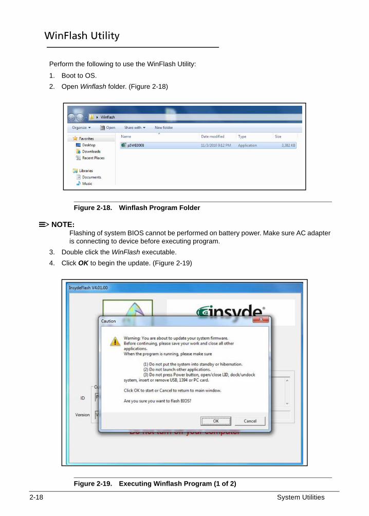
2-18 System Utilities
WinFlash Utility 0
Perform the following to use the WinFlash Utility:
1. Boot to OS.
2. Open Winflash folder. (Figure 2-18)
Figure 2-18. Winflash Program Folder
NOTE:NOTE:Flashing of system BIOS cannot be performed on battery power. Make sure AC adapter is connecting to device before executing program.
3. Double click the WinFlash executable.
4. Click OK to begin the update. (Figure 2-19)
Figure 2-19. Executing Winflash Program (1 of 2)

System Utilities 2-19
5. If the AC adapter is connected and there is no BIOS ROM file size error, a progress screen is shown. (Figure 2-20)
Figure 2-20. InsydeFlash
6. After flashing process is complete, the program will automatically restart the system.
7. If AC adapter is not connected, the following dialogs are shown. (Figure 2-21, Figure 2-22)
Figure 2-21. No AC Power Detected (1 of 2)
PXXX5 PXXX5
V 1.00V0.08

2-20 System Utilities
Figure 2-22. No AC Power Detected (2 of 2)
8. Connect AC adapter to device and repeat steps two through four.
9. If there is BIOS ROM file size error, the following dialog is shown. (Figure 2-23)
Figure 2-23. BIOS ROM File Size Error
10. If BIOS ROM file size does not match available ROM space, download correct Ignition SKU ME files for this model.
11. Copy Ignition SKU ME files to Winflash folder.
12. Repeat steps two through four.

System Utilities 2-21
HDD/BIOS Password Utilities 0
NOTE:NOTE:If Power-on Password authentication is enabled, the BIOS password can only be cleared by initiating the Crisis Disk Recovery procedure. See Chapter 5, BIOS Recovery by Crisis Disk.
Clearing HDD Passwords 0
This section provides details about clearing an HDD password from the BIOS. If the HDD password is incorrectly entered three times, an error is generated. (Figure 2-24)
Figure 2-24. Password Error Status Dialog
To reset the HDD password, perform the following:
1. Press Enter to continue. The Select Item dialog is shown. (Figure 2-25)
Figure 2-25. Select Item Dialog
2. Use the and keys to highlight Enter Unlock Password and press Enter. The Enter Unlock Password dialog is shown. (Figure 2-26)
Figure 2-26. Enter Unlock Password Dialog
Harddisk Security
Primary Master TOSHLBA MK3252GSX Lock
Select Item
Enter Unlock PasswordSystem continue
Enter Unlock Password (Key:54591747)?

2-22 System Utilities
NOTE:NOTE:A key code is generated for use with unlocking utility. Make note of this code.
3. On a separate, compatible device, boot to DOS.
4. Execute UnlockHD.exe (Figure 2-27) to create a password unlock code. Use the format <UnlockHD [key code]> with the code noted in the Figure 2-26.
Example: UnlockHD 54591747
The command generates a password which can be used for unlocking the HDD.
Password: 41499389
Figure 2-27. Unlock Password
5. On original device, enter password (Figure 2-27) in Enter Unlock Password dialog (Figure 2-28).
Figure 2-28. Unlock Password Dialog
Enter Unlock Password (Key:54591747)?

System Utilities 2-23
Clearing BIOS Passwords 0
If a BIOS password (Supervisor Password and/or User Password) is set, the BIOS will prompt for the password at system POST or upon entering the BIOS setup menu. There are two methods for clearing the BIOS password. A hardware method and a software method.
Hardware Method 0
1. Remove AC adapter.
2. Locate the RTC reset point and short it (A). (Figure 2-29)
Figure 2-29. CMOS Jumper
3. Plug in AC adapter.
4. Restart the system and press F2 to enter BIOS Utility Setup menu.
5. If no password prompt is shown, BIOS password is cleared.
6. If password prompt is shown, repeat steps 1 through 5.
Table 2-5. CMOS Jumper
Item Description
Clear CMOS Clear CMOS Jumper (RTC reset point)
A

2-24 System Utilities
Software Method 0
1. At a DOS prompt, enter clnpwd.exe.
2. Press 1 or 2 to clean the desired password. (Figure 2-30)
Figure 2-30. Clean BIOS Password
3. The on screen message shows function success or failure.
D:\Clnpwd>clnpwd
Acer Clean Password Utility V1.00
Press 1 or 2 to clean any password shown as below
1. User Password
2. Supervisor Password
Clean User Password Successful!

System Utilities 2-25
Miscellaneous Tools 0
Using Boot Sequence Selector 0
The Boot Sequence Selector allows the boot order to be changed without accessing the BIOS Setup Utility. To use the Boot Sequence Selector, perform the following:
1. At a DOS prompt, enter bs <#> and a boot sequence ID number. A boot sequence ID is a digit from 1 to 4. (Figure 2-31)
Figure 2-31. Boot Sequence Selector
Example: bs <2>, selects the boot sequence of HDD | CD ROM | LAN | Floppy.
D:\BOOTSEQd>bs
*** Boot Sequence Selector Version 0.03 ***
Created by Rockwell Chuang 10/01/2005.1.
Usage:
BS [ 1 | 2 | 3 | 4 ]
BS 1: [Floppy] => [HardDisk] => [CD-ROM] => [LAN]
BS 2: [HardDisk] => [CD-ROM] => [LAN] => [Floppy]
BS 3: [CD-ROM] => [HardDisk] => [LAN] => [Floppy]
BS 4: [LAN] => [Floppy] => [HardDisk] => [CD-ROM]
D:\BOOTSEQ>

2-26 System Utilities
Using Boot Manager 0
The Boot Manager allows the boot order to be changed without accessing the BIOS Setup Utility. To use the Boot Manager, perform the following:
NOTE:NOTE:The F12 Boot Menu option must be set to Enabled in the BIOS Setup Utility’s Main screen. (refer to Main)
To use the Boot Manager, perform the following steps:
1. Start the computer.
2. Press F12 when prompted during POST procedure. The Boot Manager dialog is shown. (Figure 2-32)
Figure 2-32. Boot Manager Dialog
3. Use the and keys to highlight a boot device.
4. Press Enter to select an option and continue the boot procedure.
Boot Manager
Boot Option Menu
1: HDD0: Hitachi HTS543216L9A300
2: ATAPI CDROM: HL-DT-ST DVDRAM GT20N
4: Network Boot: Realtek Boot Agent
and to change option, ENTER to select an option

System Utilities 2-27
Using DMITools 0
The DMI (Desktop Management Interface) Tool copies BIOS information to EEPROM (Electrically Erasable Programmable Read-Only Memory). Used in the DMI pool for hardware management.
When the BIOS shows Verifying DMI pool data, it is checking that the table correlates with installed hardware components before sending information to the operating system (Windows, etc.).
To update the DMI Pool, perform the following:
1. Boot to DOS.
2. At the prompt, enter dmitools with one of the following arguments:
/r ==> Read dmi information from memory
/wm ==> Write Manufacturer Name to EEPROM (max. 16 characters)
/wp ==> Write Product Name to EEPROM (max. 20 characters)
/ws ==> Write Serial Number to EEPROM (max. 22 characters)
/wu ==> Write UUID to EEPROM (ignore string)
/wa ==> Write Asset Tag to EEPROM (max. 32 characters)
The following examples show the commands and the corresponding output information:
Read DMI Information from Memory
Input: 0
dmitools /r
Output: 0
Manufacturer (Type1, Offset04h): Acer
Product Name (Type1, Offset05h): Aspire
Serial Number (Type1, Offset07h): 01234567890123456789
UUID String (Type1, Offset08h): xxxxxxxx-xxxx-xxxx-xxxx-xxxxxxxxxxxx
Asset Tag (Type3, Offset04h): Acer Asstag
Write Manufacturer Name to EEPROM
Input: 0
dmitools /wm Acer
Write Product Name to EEPROM
Input: 0
dmitools /wp Acer

2-28 System Utilities
Write Serial Number to EEPROM
Input: 0
dmitools /ws 01234567890123456789
Write UUID to EEPROM
Input: 0
dmitools /wu
Write Asset Tag to EEPROM
Input: 0
dmitools /wa Acer Asstag
NOTE:NOTE:For examples two (2) through six (6), restart the system to write any changes in the data to the EEPROM.

System Utilities 2-29
Using LAN MAC EEPROM Utility 0
Use MAC.BAT utility to write the MAC.CFG file to EEPROM under DOS mode.
1. Edit MAC.CFG to add correct WriteData, StartAddr, and WriteLeng values. (Figure 2-33)
Figure 2-33. MAC.CFG File
2. In DOS mode, run MAC.BAT to write MAC values to eeprom. (Figure 2-34)
Figure 2-34. Updating EEPROM with MAC.BAT
3. Reboot computer when process has completed.
Field Name Value Description
Title MAC Address byte
N/A
WriteData ‘001122334455’ MAC value
StartAddr 7A MAC address
WriteLeng 6 MAC value length
KeepByte 0 N/A

2-30 System Utilities

CHAPTER 3
Machine Maintenance Procedures

3-2
Introduction . . . . . . . . . . . . . . . . . . . . . . . . . . . . . . . . . . . . . . . . . 3-5General Information . . . . . . . . . . . . . . . . . . . . . . . . . . . . . . . . . . 3-5Recommended Equipment . . . . . . . . . . . . . . . . . . . . . . . . . . . . . 3-5Maintenance Flowchart. . . . . . . . . . . . . . . . . . . . . . . . . . . . . . . . 3-6Getting Started . . . . . . . . . . . . . . . . . . . . . . . . . . . . . . . . . . . . . . 3-7
Dummy Card Removal . . . . . . . . . . . . . . . . . . . . . . . . . . . . . . 3-8Dummy Card Installation . . . . . . . . . . . . . . . . . . . . . . . . . . . . 3-8Battery Removal . . . . . . . . . . . . . . . . . . . . . . . . . . . . . . . . . . . 3-9Battery Installation. . . . . . . . . . . . . . . . . . . . . . . . . . . . . . . . . 3-9ODD Module Removal . . . . . . . . . . . . . . . . . . . . . . . . . . . . . . 3-11ODD Module Installation . . . . . . . . . . . . . . . . . . . . . . . . . . . . 3-13Logic Door Removal . . . . . . . . . . . . . . . . . . . . . . . . . . . . . . . . 3-14Logic Door Installation. . . . . . . . . . . . . . . . . . . . . . . . . . . . . . 3-14Main and Secondary HDD Module Removal . . . . . . . . . . . . 3-15Main and Secondary HDD Module Installation . . . . . . . . . . 3-17Main and Secondary HDD Module Carrier Removal . . . . . . 3-18Main and Secondary HDD Module Carrier Installation . . . . 3-19WLAN Module Removal. . . . . . . . . . . . . . . . . . . . . . . . . . . . . 3-20WLAN Module Installation . . . . . . . . . . . . . . . . . . . . . . . . . . 3-21DIMM Module Removal . . . . . . . . . . . . . . . . . . . . . . . . . . . . . 3-22DIMM Module Installation. . . . . . . . . . . . . . . . . . . . . . . . . . . 3-23Keyboard Removal . . . . . . . . . . . . . . . . . . . . . . . . . . . . . . . . . 3-24Keyboard Installation. . . . . . . . . . . . . . . . . . . . . . . . . . . . . . . 3-26Upper Cover Removal . . . . . . . . . . . . . . . . . . . . . . . . . . . . . . 3-27Upper Cover Installation . . . . . . . . . . . . . . . . . . . . . . . . . . . . 3-30Touchpad FFC Removal . . . . . . . . . . . . . . . . . . . . . . . . . . . . . 3-32Touchpad FFC Installation . . . . . . . . . . . . . . . . . . . . . . . . . . . 3-33Power Board Removal . . . . . . . . . . . . . . . . . . . . . . . . . . . . . . 3-34Power Board Installation . . . . . . . . . . . . . . . . . . . . . . . . . . . . 3-35RJ45 Module Removal . . . . . . . . . . . . . . . . . . . . . . . . . . . . . . 3-36RJ45 Module Installation . . . . . . . . . . . . . . . . . . . . . . . . . . . . 3-37USB Module Removal. . . . . . . . . . . . . . . . . . . . . . . . . . . . . . . 3-38USB Module Installation . . . . . . . . . . . . . . . . . . . . . . . . . . . . 3-39Bluetooth Module Removal. . . . . . . . . . . . . . . . . . . . . . . . . . 3-40Bluetooth Module Installation . . . . . . . . . . . . . . . . . . . . . . . 3-41RTC Battery Removal . . . . . . . . . . . . . . . . . . . . . . . . . . . . . . . 3-42RTC Battery Installation . . . . . . . . . . . . . . . . . . . . . . . . . . . . . 3-42Speaker Module Removal . . . . . . . . . . . . . . . . . . . . . . . . . . . 3-43Speaker Module Installation . . . . . . . . . . . . . . . . . . . . . . . . . 3-44Mainboard Removal. . . . . . . . . . . . . . . . . . . . . . . . . . . . . . . . 3-45Mainboard Installation . . . . . . . . . . . . . . . . . . . . . . . . . . . . . 3-47Thermal Fan Module Removal. . . . . . . . . . . . . . . . . . . . . . . . 3-48Thermal Fan Module Installation . . . . . . . . . . . . . . . . . . . . . 3-49Thermal Module Removal . . . . . . . . . . . . . . . . . . . . . . . . . . . 3-50Thermal Module Installation . . . . . . . . . . . . . . . . . . . . . . . . . 3-51CPU Removal. . . . . . . . . . . . . . . . . . . . . . . . . . . . . . . . . . . . . . 3-52CPU Installation . . . . . . . . . . . . . . . . . . . . . . . . . . . . . . . . . . . 3-52

3-3
PCH Heatsink Removal . . . . . . . . . . . . . . . . . . . . . . . . . . . . . . 3-53PCH Heatsink Installation. . . . . . . . . . . . . . . . . . . . . . . . . . . . 3-53LCD Module Removal. . . . . . . . . . . . . . . . . . . . . . . . . . . . . . . 3-54LCD Module Installation . . . . . . . . . . . . . . . . . . . . . . . . . . . . 3-56DC-IN Cable Removal . . . . . . . . . . . . . . . . . . . . . . . . . . . . . . . 3-57DC-IN Cable Installation. . . . . . . . . . . . . . . . . . . . . . . . . . . . . 3-58LCD Bezel Removal. . . . . . . . . . . . . . . . . . . . . . . . . . . . . . . . . 3-59LCD Bezel Installation . . . . . . . . . . . . . . . . . . . . . . . . . . . . . . 3-60CCD Module Removal . . . . . . . . . . . . . . . . . . . . . . . . . . . . . . 3-63CCD Module Installation . . . . . . . . . . . . . . . . . . . . . . . . . . . . 3-63LCD Panel Removal. . . . . . . . . . . . . . . . . . . . . . . . . . . . . . . . . 3-64LCD Panel Installation . . . . . . . . . . . . . . . . . . . . . . . . . . . . . . 3-65LCD Brackets Removal . . . . . . . . . . . . . . . . . . . . . . . . . . . . . . 3-67LCD Brackets Installation . . . . . . . . . . . . . . . . . . . . . . . . . . . . 3-67LVDS Cable Removal . . . . . . . . . . . . . . . . . . . . . . . . . . . . . . . 3-68LVDS Cable Installation . . . . . . . . . . . . . . . . . . . . . . . . . . . . . 3-69Microphone Module Removal . . . . . . . . . . . . . . . . . . . . . . . . 3-70Microphone Module Installation. . . . . . . . . . . . . . . . . . . . . . 3-70WLAN Antenna Removal . . . . . . . . . . . . . . . . . . . . . . . . . . . . 3-71WLAN Antenna Installation. . . . . . . . . . . . . . . . . . . . . . . . . . 3-71

3-4

Machine Maintenance Procedures 3-5
Machine Maintenance Procedures
Introduction 0
This chapter contains general information about the notebook, a list of tools needed to perform the required maintenance and step by step procedures on how to remove and install components from the notebook computer.
General Information 0
The product previews seen in the following procedures may not represent the final product color or configuration. Cable paths and positioning may also differ from the actual model. During the removal and installation of components, make sure all available cable channels and clips are used and that the cables are installed in the same position.
All prerequisites must be performed prior to performing maintenance.
Recommended Equipment 0
The following tools are required to perform maintenance on the notebook:
Wrist grounding strap and conductive mat
Flat screwdriver
Philips screwdriver
Table 3-1. Main Screw Table
Screw Name Quantity
M2.5x6.0 27
M2.0x3.0 11
M2.5x3.0 Ni 7
M3.0x3.0 Ni 4
M2.0x3.0 t=0.8 8D 4
M2.5x5.0 6
M2.0x5.0 2
M2.5x3.2 w/spring Ni 4
M2.5x3.0 4

3-6 Machine Maintenance Procedures
Maintenance Flowchart 0
The flowchart in Figure 3-1 provides a graphic representation of the module removal and installation sequences. It provides information on what components need to be removed and installed during servicing.
Figure 3-1. Maintenance Flow

Machine Maintenance Procedures 3-7
Getting Started 0
The flowchart (Figure 3-1) identifies sections illustrating the entire removal and install sequence. Observe the order of the sequence to avoid damage to any of the hardware components.
Perform the following prior to performing any maintenance procedures:
1. Remove power (A) from the system and peripherals. (Figure 3-2)
Figure 3-2. AC Adapter
2. Remove all cables from system.
A

3-8 Machine Maintenance Procedures
Dummy Card Removal 0
1. Push in dummy card (A) to release from spring latch. (Figure 3-3)
Figure 3-3. Dummy Card
2. Remove dummy card (A).
Dummy Card Installation 0
1. Insert dummy card (A). (Figure 3-3)
2. Push in card until spring latch locks.
A

Machine Maintenance Procedures 3-9
Battery Removal 0
1. Slide battery lock switch (A) to the unlock position. (Figure 3-4)
Figure 3-4. Battery
IMPORTANT:?Follow local regulations for battery disposal.
2. Use slot (B) to pull battery (C) from battery bay and remove battery from lower cover.
Battery Installation 0
1. Align flanges (D) on battery to slots (E) in battery bay. (Figure 3-5 and Figure 3-6)
Figure 3-5. Battery Flanges
C
A B
D

3-10 Machine Maintenance Procedures
Figure 3-6. Battery Bay Slots
2. Press battery (C) to secure to lower cover. (Figure 3-4)
3. Make sure battery lock switch (A) is in lock position.
E

Machine Maintenance Procedures 3-11
ODD Module Removal 0
Prerequisite:
Battery Removal
1. Remove screw (A) from lower cover. (Figure 3-7)
Figure 3-7. ODD Module Lower Cover Screw
2. Remove module (B) from lower cover bay. (Figure 3-8)
Figure 3-8. ODD Module
A
B

3-12 Machine Maintenance Procedures
3. Insert thin tool to release ODD tray from module. (Figure 3-9)
Figure 3-9. Releasing ODD Module Tray (1 of 2)
4. Unlock bezel locking latch from module tray. (Figure 3-10)
Figure 3-10. Releasing ODD Module Tray (2 of 2)
5. Remove bezel (C) from module.
C

Machine Maintenance Procedures 3-13
6. Remove screws (D) from module bracket (E). (Figure 3-11)
Figure 3-11. ODD Module Bracket and Screws
7. Remove bracket from module.
ODD Module Installation 0
1. Install bracket (E) on module. (Figure 3-11)
2. Install and secure screws (D) to module bracket (E).
3. Install bezel (C) on module. (Figure 3-10)
4. Secure bezel locking latch to module tray.
5. Slide tray into module. (Figure 3-9)
6. Install module (B) in lower cover bay. (Figure 3-8)
7. Install and secure screw (A) to lower cover. (Figure 3-7)
8. Install battery.
ID Size Quantity Screw Type
A M2.5x6.0 1
D M2.0x3.0 2
D
E

3-14 Machine Maintenance Procedures
Logic Door Removal 0
Prerequisite:
ODD Module Removal
1. Loosen captive screws (A) on logic door. (Figure 3-12)
Figure 3-12. Logic Door
2. Using slot (B) lift logic door (C) from lower cover.
3. Remove logic door.
Logic Door Installation 0
1. Install logic door on lower cover. (Figure 3-12)
2. Press edges of logic door to secure locking latches on lower cover.
3. Tighten captive screws (A) to logic door.
4. Install ODD module.
A
BC

Machine Maintenance Procedures 3-15
Main and Secondary HDD Module Removal 0
Prerequisite:
Logic Door Removal
NOTE:NOTE:The following procedure is used for both the main and secondary HDD modules.
1. Locate HDD module (A) on lower cover. (Figure 3-13)
Figure 3-13. Main HDD Module
2. Remove screws (B) from lower cover. (Figure 3-14)
Figure 3-14. Main HDD Module Screws
A
B

3-16 Machine Maintenance Procedures
3. Disconnect HDD connector (D) from mainboard connector (E) using mylar tab (C). (Figure 3-15 and Figure 3-16)
Figure 3-15. Removing HDD Module (1 of 2)
Figure 3-16. Removing HDD Module (2 of 2)
4. Remove module from lower cover.
C
D
E

Machine Maintenance Procedures 3-17
Main and Secondary HDD Module Installation 0
NOTE:NOTE:The following procedure is used for both the main and secondary HDD modules.
1. Install HDD (A) on lower cover. (Figure 3-16)
2. Connect HDD connector (D) to mainboard connector (E) using plastic tab (C). (Figure 3-15)
3. Install and secure screws (B) to lower cover. (Figure 3-14)
4. Install logic door.
ID Size Quantity Screw Type
B M2.5x3.0 Ni 2

3-18 Machine Maintenance Procedures
Main and Secondary HDD Module Carrier Removal 0
Prerequisite:
Main and Secondary HDD Module Removal
NOTE:NOTE:The following procedure is used for both the main and secondary HDD module carriers.
1. Remove screws (A) from carrier. (Figure 3-17)
Figure 3-17. HDD Module Carrier Screws
2. Remove left and right brackets (B) from module.
3. Remove mylar covering (C) from module. (Figure 3-18)
Figure 3-18. HDD Carrier Mylar Covering
AB
C

Machine Maintenance Procedures 3-19
Main and Secondary HDD Module Carrier Installation 0
NOTE:NOTE:The following procedure is used for both the main and secondary HDD module carriers.
1. Secure mylar cover (C) to module. (Figure 3-18)
2. Install left and right brackets (B) on module. (Figure 3-17)
3. Install and secure screws (A) to carrier.
4. Install HDD module.
ID Size Quantity Screw Type
A M3.0x3.0 Ni 4

3-20 Machine Maintenance Procedures
WLAN Module Removal 0
Prerequisite:
Logic Door Removal
1. Locate WLAN module (A) on lower cover. (Figure 3-19)
Figure 3-19. WLAN Module
2. Disconnect main (B) and auxiliary (C) antennas from WLAN board connectors. (Figure 3-20)
Figure 3-20. WLAN Antennas
A
B
C

Machine Maintenance Procedures 3-21
3. Remove screw (D) from module. (Figure 3-21)
Figure 3-21. WLAN Module Screw
4. Disconnect module (A) from mainboard connector (E).
5. Remove module from lower cover.
WLAN Module Installation 0
1. Install and connect module to mainboard connector. (Figure 3-21)
2. Install and secure screw (D) to module.
3. Connect main (B) and auxiliary (C) antennas to module connectors. (Figure 3-20)
4. Install logic door.
ID Size Quantity Screw Type
D M2.0x3.0 1
D
E A

3-22 Machine Maintenance Procedures
DIMM Module Removal 0
Prerequisite:
WLAN Module Screw
1. Locate DIMM module (A) on lower cover. (Figure 3-22)
Figure 3-22. DIMM Module
2. Release DIMM from module clips (B). (Figure 3-23)
Figure 3-23. DIMM Module Clips
3. Disconnect module (A) from mainboard connector (C).
4. Repeat steps 1 and 2 for remaining DIMM modules.
A
BA
C

Machine Maintenance Procedures 3-23
DIMM Module Installation 0
1. Connect DIMM module (A) to mainboard connector (A). (Figure 3-23)
2. Secure DIMM in module clips (B).
3. Repeat steps 1 and 2 for remaining DIMM modules.
4. Install logic door.

3-24 Machine Maintenance Procedures
Keyboard Removal 0
Prerequisite:
Logic Door Removal
1. Locate keyboard (A) on upper cover. (Figure 3-24)
Figure 3-24. Keyboard
2. Starting from the top center of keyboard, unlock eight latches (B) securing keyboard to upper cover. (Figure 3-24 and Figure 3-25)
Figure 3-25. Removing Keyboard (1 of 3)
A
B
BB
B

Machine Maintenance Procedures 3-25
CAUTION:!Keyboard FPC is connected to mainboard connector. Lift with caution.
3. Lift keyboard from upper cover. (Figure 3-26)
Figure 3-26. Removing Keyboard (2 of 3)
4. Put keyboard (A) face-down on upper cover to show keyboard FPC (C). (Figure 3-27)
Figure 3-27. Removing Keyboard (3 of 3)
5. Disconnect FPC from mainboard connector (D).
6. Remove keyboard from upper cover.
C
D
A

3-26 Machine Maintenance Procedures
Keyboard Installation 0
1. Put keyboard (A) face-down on upper cover to show keyboard FPC (C). (Figure 3-27)
2. Connect FPC (C) to mainboard connector (D).
3. Align keyboard flanges (E) with upper cover slots (F). (Figure 3-28)
Figure 3-28. Keyboard Flanges and Upper Cover Slots
4. Install keyboard on upper cover.
5. Secure eight latches (B) of upper cover to keyboard. (Figure 3-24)
6. Install logic door.
F
E

Machine Maintenance Procedures 3-27
Upper Cover Removal 0
NOTE:NOTE:Only the secondary HDD module is a prerequisite to remove the upper cover.
Prerequisite:
Main and Secondary HDD Module Removal
1. Remove screws (A) from lower cover. (Figure 3-29)
Figure 3-29. Lower Cover Screws
2. Show upper cover. (Figure 3-30)
Figure 3-30. Upper Cover FFC and Mainboard Connectors
3. Disconnect power board FFC (A) from mainboard connector (B).
A A
A
BC
D

3-28 Machine Maintenance Procedures
4. Disconnect touchpad FFC (C) from mainboard connector (D).
5. Remove screws (E) from upper cover. (Figure 3-31)
Figure 3-31. Upper Cover Screws
6. Place thumb in odd bay (F) and lift right side of upper cover to release locking latches of lower cover. (Figure 3-32)
Figure 3-32. Removing Upper Cover (1 of 2)
E
F
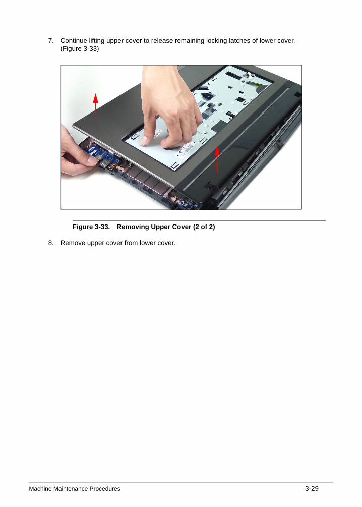
Machine Maintenance Procedures 3-29
7. Continue lifting upper cover to release remaining locking latches of lower cover. (Figure 3-33)
Figure 3-33. Removing Upper Cover (2 of 2)
8. Remove upper cover from lower cover.

3-30 Machine Maintenance Procedures
Upper Cover Installation 0
1. Align top edge (G) of upper cover with lower cover. (Figure 3-34)
Figure 3-34. Installing Upper Cover (1 of 3)
2. Secure remaining upper cover locking latches to lower cover. (Figure 3-35)
Figure 3-35. Installing Upper Cover (2 of 3)
G

Machine Maintenance Procedures 3-31
Figure 3-36. Installing Upper Cover (3 of 3)
3. Install and secure screws (E) to upper cover. (Figure 3-31)
4. Connect touchpad FFC (C) to mainboard connector (D). (Figure 3-30)
5. Connect power board FFC (A) to mainboard connector (B).
6. Show lower cover. (Figure 3-29)
7. Install and secure screws (A) to lower cover.
8. Install secondary HDD module.
ID Size Quantity Screw Type
A M2.5x6.0 18
E M2.5x6.0 3

3-32 Machine Maintenance Procedures
Touchpad FFC Removal 0
Prerequisite:
Upper Cover Removal
1. Locate touchpad board (A) on upper cover. (Figure 3-38)
Figure 3-37. Touchpad Board
2. Remove tape (B) securing touchpad FFC and board connector. (Figure 3-38)
Figure 3-38. Touchpad Board FFC Tape
A
B

Machine Maintenance Procedures 3-33
3. Disconnect touchpad FFC (C) from board connector (D). (Figure 3-39)
Figure 3-39. Touchpad FFC and Touchpad Connector
4. Remove FFC from touchpad board.
Touchpad FFC Installation 0
1. Install touchpad FFC (C) on touchpad board (A). (Figure 3-39)
2. Connect touchpad FFC (C) to board connector (D).
3. Install tape (B) securing touchpad FFC and board connector. (Figure 3-38)
4. Install upper cover.
D
C
A

3-34 Machine Maintenance Procedures
Power Board Removal 0
Prerequisite:
Upper Cover Removal
1. Locate power board (A) on upper cover. (Figure 3-40)
Figure 3-40. Power Board
2. Remove tape (B) securing sleep sensor board to upper cover. (Figure 3-41)
Figure 3-41. Sleep Sensor Tape
A
B

Machine Maintenance Procedures 3-35
3. Remove sleep sensor board (C) from upper cover guides (D). (Figure 3-42)
Figure 3-42. Sleep Sensor Board
4. Remove screws (E) from power board. (Figure 3-43)
Figure 3-43. Power Board Screws
5. Remove power board and sleep sensor board from upper cover.
Power Board Installation 0
1. Install power board on upper cover. (Figure 3-43)
2. Install and secure screws (E) to power board.
3. Align and install sleep sensor board (C) in upper cover guides (D). (Figure 3-42)
4. Install tape (B) securing sleep sensor board to upper cover. (Figure 3-41)
ID Size Quantity Screw Type
E M2.5x3.0 Ni 2
C
D
D
E

3-36 Machine Maintenance Procedures
RJ45 Module Removal 0
Prerequisite:
Upper Cover Removal
1. Locate RJ45 module (A) on lower cover. (Figure 3-44)
Figure 3-44. RJ45 Module
2. Remove tape (B) securing RJ45 cable to mainboard connector.
3. Disconnect RJ45 cable (C) (disconnected) from mainboard connector (D). (Figure 3-45)
Figure 3-45. RJ45 Cable / Connector
4. Remove screw (E) from board.
A
B
C
D
E

Machine Maintenance Procedures 3-37
5. Remove module from lower cover.
6. Remove tape (F) securing RJ45 cable (C) to module connector (G). (Figure 3-46)
Figure 3-46. Removing RJ45 Cable (1 of 2)
7. Disconnect cable (C) from module connector (G). (Figure 3-47)
Figure 3-47. Removing RJ45 Cable (2 of 2)
RJ45 Module Installation 0
1. Connect cable (C) to module connector (G). (Figure 3-47)
2. Install tape (F) securing RJ45 cable (C) to module connector (G). (Figure 3-46)
3. Install module on lower cover. (Figure 3-45)
4. Install and secure screw (E) to module.
5. Connect RJ45 cable (C) (disconnected) to mainboard connector (D). (Figure 3-44)
6. Install tape (B) securing RJ45 cable to mainboard connector.
7. Install upper cover.
ID Size Quantity Screw Type
E M2.5x3.0 Ni 1
F
G
C
C G

3-38 Machine Maintenance Procedures
USB Module Removal 0
Prerequisite:
Upper Cover Removal
1. Locate USB module (A) on lower cover. (Figure 3-48)
Figure 3-48. USB Module
2. Remove tape (B) securing USB FFC (C) to lower cover. (Figure 3-49)
Figure 3-49. USB Module FFC
3. Disconnect FFC (C) from mainboard connector (D).
4. Remove screw (E) from module.
5. Remove module from lower cover.
A
C
DE
B

Machine Maintenance Procedures 3-39
USB Module Installation 0
1. Align module with lower cover guides (F) and USB port slots (G). (Figure 3-50)
Figure 3-50. USB Module Guides
2. Install module on lower cover.
3. Install and secure screw (E) to module. (Figure 3-49)
4. Connect FFC (C) to mainboard connector (D).
5. Install tape (B) securing USB FFC (C) to lower cover.
6. Install upper cover.
ID Size Quantity Screw Type
E M2.5x3.0 Ni 1
GF

3-40 Machine Maintenance Procedures
Bluetooth Module Removal 0
Prerequisite:
Upper Cover Removal
1. Locate Bluetooth module (A) on lower cover. (Figure 3-51)
Figure 3-51. Bluetooth Module
2. Remove tape (B) securing cable and connector to mainboard. (Figure 3-52)
Figure 3-52. Bluetooth Module and Tape
A
B

Machine Maintenance Procedures 3-41
3. Disconnect Bluetooth cable (C) from mainboard connector (D). (Figure 3-53)
Figure 3-53. Bluetooth Cable and Mainboard Connector
4. Remove module (A) from lower cover.
5. Disconnect Bluetooth cable (C) from module connector (E). (Figure 3-54)
Figure 3-54. Bluetooth Module and Cable
Bluetooth Module Installation 0
1. Connect Bluetooth cable (C) to module connector (E). (Figure 3-54)
2. Install module (A) on lower cover. (Figure 3-53)
3. Connect Bluetooth cable (C) to mainboard connector (D).
4. Install tape (B) securing cable and connector to mainboard. (Figure 3-52)
5. Install upper cover.
C
D
A
CE

3-42 Machine Maintenance Procedures
RTC Battery Removal 0
Prerequisite:
Upper Cover Removal
1. Locate RTC battery on mainboard. (Figure 3-55)
Figure 3-55. RTC Battery
2. Remove battery (A) from mainboard connector (B). (Figure 3-56)
Figure 3-56. RTC Battery and Mainboard Connector
RTC Battery Installation 0
1. Install and secure RTC battery (A) in mainboard connector (B). (Figure 3-56)
2. Install upper cover.
A
A
B

Machine Maintenance Procedures 3-43
Speaker Module Removal 0
Prerequisite:
Upper Cover Removal
1. Locate speaker modules on mainboard. (Figure 3-57)
Figure 3-57. Speaker Modules
2. Disconnect cable (B) from mainboard connector (C). (Figure 3-58)
Figure 3-58. Speaker Cable and Mainboard Connector
A
B
C

3-44 Machine Maintenance Procedures
3. Remove screws (D) from modules. (Figure 3-59)
Figure 3-59. Speaker Screws
4. Release cable (E) from lower cover guides (F).
5. Remove speaker modules.
Speaker Module Installation 0
1. Install speaker modules (A) on lower cover. (Figure 3-59)
2. Install and secure cable (E) in lower cover guides (F).
3. Install and secure screws (D) to modules.
4. Connect cable (B) to mainboard connector (C). (Figure 3-58)
5. Install upper cover.
ID Size Quantity Screw Type
D M2.0x3.0 t=0.8 8D
4
D D
E
F
A
A

Machine Maintenance Procedures 3-45
Mainboard Removal 0
Prerequisite:
Upper Cover Removal
1. Remove tape (A) securing the USB FFC (B) to the lower cover. (Figure 3-60)
Figure 3-60. Mainboard
2. Remove tape (C) securing the Bluetooth cable (E) to the lower cover.
3. Disconnect the following cables from mainboard connectors:
USB (B, D)
Bluetooth (E, F)
LVDS (G, H)
Speakers (J, K)
Microphone (L, M)
RJ45 (N, P)
4. Disconnect DC-IN cable (Q) from connector (R) on top of mainboard. (Figure 3-61)
Figure 3-61. DC-IN Cable and Mainboard Connector
D
B A
C
F E
H
G J
K
NP
ML
Q
R

3-46 Machine Maintenance Procedures
CAUTION:!Make sure cables are clear of mainboard before removing mainboard from lower cover.
5. Remove screw (S) from mainboard. (Figure 3-62)
Figure 3-62. Mainboard Screw
NOTE:NOTE:Make sure to free the VGA, HDMI, and USB ports, headphone and microphone jacks from the left side (T) of the lower cover before removing mainboard.
6. Lift and remove mainboard from lower cover as shown by arrows 1 and 2. (Figure 3-63)
Figure 3-63. Removing Mainboard
S
T
1
2

Machine Maintenance Procedures 3-47
Mainboard Installation 0
1. Align mainboard ports with lower cover slots (T). (Figure 3-63)
2. Install the mainboard on the lower cover.
3. Install and secure screw (S) to the mainboard. (Figure 3-62)
4. Connect the DC-IN cable (Q) to connector (R) on top of mainboard. (Figure 3-61)
5. Connect the following cables to the mainboard connectors: (Figure 3-60)
USB (B, D)
Bluetooth (E, F)
LVDS (G, H)
Speakers (J, K)
Microphone (L, M)
RJ45 (N, P)
6. Install the tape (C) securing the Bluetooth cable (E) to the lower cover.
7. Install the tape (A) securing the USB FFC (B) to the lower cover.
8. Install the upper cover.
ID Size Quantity Screw Type
S M2.5x3.0 1

3-48 Machine Maintenance Procedures
Thermal Fan Module Removal 0
Prerequisite:
Mainboard Removal
1. Locate thermal fan module (A) on mainboard. (Figure 3-64)
Figure 3-64. Thermal Fan Module
2. Disconnect cable (B) from mainboard connector (C). (Figure 3-65)
Figure 3-65. Thermal Fan Module Cable and Screw
3. Remove screws (D) from module.
4. Remove fan (A) from mainboard.
A
B
CD
A

Machine Maintenance Procedures 3-49
Thermal Fan Module Installation 0
1. Install the fan (A) on the mainboard. (Figure 3-65)
2. Install and secure the screws (D) to the module.
3. Connect the cable (B) to the mainboard connector (C).
4. Install the mainboard.
ID Size Quantity Screw Type
B M2.0x5.0 2

3-50 Machine Maintenance Procedures
Thermal Module Removal 0
Prerequisite:
Mainboard Removal
1. Locate the thermal module (A) on the mainboard. (Figure 3-66)
Figure 3-66. Thermal Module
2. Remove CPU screws (B1 to B4) from module. (Figure 3-67)
Figure 3-67. Thermal Module Screws
3. Remove VGA screws (C5 to C6) from module.
4. Remove thermal module (A) from mainboard.
A
B1
B2
B3
B4
C5
C6
A

Machine Maintenance Procedures 3-51
Thermal Module Installation 0
IMPORTANT:?Apply suitable thermal grease and make sure all heat pads are in place before replacing module.
CAUTION:!Thermal grease can damage mainboard. Use caution when applying.
The following thermal pad types are approved for use:
VGA Pads
EAPUS/PSX
Other Pads
Laird/Tflex 340
EAPUS/XR-HL
The following thermal grease types are approved for use:
I-Connoisseur/N302
Honeywell
1. Remove all traces of thermal grease from CPU using a lint-free cloth or cotton swab and Isopropyl Alcohol, Acetone, or other approved cleaning agent.
2. Apply small amount of thermal grease to center of CPU (E). (Figure 3-68)
NOTE:NOTE:Force used during installation of thermal assembly is sufficient to spread grease over CPU.
Figure 3-68. Thermal Module Installation
3. Align module to mainboard screw holes.
4. Install and secure screws (B1 to B4) in numerical order to mainboard. (Figure 3-67)
5. Install and secure screws (C5 to C6) to mainboard.
6. Install lower cover.
ID Size Quantity Screw Type
B1-B4 M2.5x3.2 w/spring Ni 4
C5-C6 M2.5x3.0 2
E

3-52 Machine Maintenance Procedures
CPU Removal 0
Prerequisite:
Thermal Module Removal
1. Unlock CPU from mainboard socket by rotating captive screw (A) left 180º. (Figure 3-69)
Figure 3-69. CPU
2. Lift CPU (C) from socket.
CPU Installation 0
1. Align CPU marker (B) with socket marker (C). (Figure 3-69)
2. Install CPU (C) in socket.
3. Lock CPU in socket by rotating screw (A) right 180º.
4. Install thermal module.
A
C
B
C

Machine Maintenance Procedures 3-53
PCH Heatsink Removal 0
Prerequisite:
Mainboard Removal
1. Locate the PCH heatsink (A) on the mainboard. (Figure 3-70)
Figure 3-70. PCH Heatsink
2. Remove screws (B) from mainboard.
3. Remove heatsink (A) from mainboard.
PCH Heatsink Installation 0
1. Install heatsink (A) on mainboard. (Figure 3-70)
2. Install and secure screws (B) to heatsink.
3. Install mainboard on lower cover
ID Size Quantity Screw Type
B M2.5x3.0 2
A B

3-54 Machine Maintenance Procedures
LCD Module Removal 0
Prerequisite:
RJ45 Module Removal
Speaker Module Removal
1. Remove WLAN antennas (A) from lower cover guides (B). (Figure 3-71 and Figure 3-72)
Figure 3-71. Removing WLAN Antennas (1 of 2)
Figure 3-72. Removing WLAN Antennas (2 of 2)
A
B
B

Machine Maintenance Procedures 3-55
2. Remove screws (C) from LCD hinges. (Figure 3-73 and Figure 3-74)
Figure 3-73. Removing LCD Hinge Screws (1 of 2)
Figure 3-74. Removing LCD Hinge Screws (2 of 2)
3. Remove module (D) from lower cover. (Figure 3-75)
Figure 3-75. LCD Module
C
C
D
E

3-56 Machine Maintenance Procedures
LCD Module Installation 0
1. Align LCD hinges (E) with lower cover. (Figure 3-75)
2. Install module (D) on lower cover.
3. Install and secure screws (C) to LCD hinges. (Figure 3-73 and Figure 3-74)
4. Install WLAN antennas (A) in lower cover guides (B). (Figure 3-71 and Figure 3-72)
5. Install RJ45 module.
6. Install speaker modules.
ID Size Quantity Screw Type
C M2.5x6.0 5

Machine Maintenance Procedures 3-57
DC-IN Cable Removal 0
Prerequisite:
LCD Module Removal
1. Locate DC-IN cable (A) on lower cover. (Figure 3-76)
Figure 3-76. DC-IN Cable
2. Remove cable (A) from lower cover guides (B). (Figure 3-77)
Figure 3-77. DC-IN Cable
3. Remove DC-IN jack (C) from lower cover guide (D).
A
A
B
C
D

3-58 Machine Maintenance Procedures
DC-IN Cable Installation 0
1. Install DC-IN jack (C) in lower cover guide (D). (Figure 3-77)
2. Install cable (A) in lower cover guides (B).
3. Install LCD module.

Machine Maintenance Procedures 3-59
LCD Bezel Removal 0
Prerequisite:
LCD Module Removal
1. Remove screws (A) from bezel. (Figure 3-78)
Figure 3-78. LCD Bezel Screws
2. Starting from the top of the LCD bezel, unlock bezel from LCD cover locking latches. (Figure 3-79)
Figure 3-79. Removing LCD Bezel (1 of 2)
A

3-60 Machine Maintenance Procedures
3. Continue with the left, right and bottom sides of bezel until all locking latches have been released. (Figure 3-80)
Figure 3-80. Removing LCD Bezel (2 of 2)
4. Remove bezel from LCD cover.
LCD Bezel Installation 0
CAUTION:!Antenna and microphone cables may be damaged by the bezel when securing it to the LCD cover. Make sure cables are placed in LCD hinge wells.
1. Align bezel hinge covers (A) with LCD hinge wells (B). (Figure 3-81 and Figure 3-82)
Figure 3-81. LCD Bezel Hinge Covers and LCD Cover Wells (1 of 2)
A
B

Machine Maintenance Procedures 3-61
Figure 3-82. LCD Bezel Hinge Covers and LCD Cover Wells (2 of 2)
2. Starting at the bottom of the bezel, secure the bezel to the LCD cover locking latches. (Figure 3-83)
Figure 3-83. Securing the LCD Bezel (1 of 3)
AB

3-62 Machine Maintenance Procedures
3. Continue with the left, right and bottom sides of bezel until all locking latches have been secured. (Figure 3-84 and Figure 3-85)
Figure 3-84. Securing the LCD Bezel (2 of 3)
Figure 3-85. Securing the LCD Bezel (3 of 3)
4. Install and secure screws (A) to bezel. (Figure 3-78)
5. Install LCD Module.
ID Size Quantity Screw Type
A M2.5x6.0 2

Machine Maintenance Procedures 3-63
CCD Module Removal 0
Prerequisite:
LCD Bezel Removal
1. Locate CCD module on LCD cover. (Figure 3-86)
Figure 3-86. CCD Module
2. Disconnect cable (B) from connector (C). (Figure 3-87)
Figure 3-87. CCD Cable
3. Remove foil tab (D) covering cable.
4. Remove module (A) from lower cover.
CCD Module Installation 0
1. Install module (A) on lower cover. (Figure 3-87)
2. Install foil tab (D) to cover CCD cable.
3. Connect cable (B) to board connector (C).
A
BC D

3-64 Machine Maintenance Procedures
LCD Panel Removal 0
Prerequisite:
LCD Bezel Removal
1. Remove screws (A) from panel. (Figure 3-88)
Figure 3-88. LCD Panel Screws
2. Remove LVDS cable (B) from guides (C) on LCD cover. (Figure 3-89)
Figure 3-89. LVDS Cable and LCD Cover Guides
3. Remove panel (D) from LCD cover.
A A
B
CD

Machine Maintenance Procedures 3-65
LCD Panel Installation 0
1. Locate the LCD cover panel guide pins (E). (Figure 3-90 and Figure 3-91)
Figure 3-90. LCD Cover Panel Guide Pins (1 of 2)
Figure 3-91. LCD Cover Panel Guide Pins (2 of 2)
2. Align panel brackets with lower cover top guide pins. (Figure 3-92)
Figure 3-92. Installing the LCD Panel (1 of 2)
E
E

3-66 Machine Maintenance Procedures
3. Align panel brackets with lower cover bottom guide pins. (Figure 3-93)
Figure 3-93. Installing the LCD Panel (2 of 2)
4. Install panel on lower cover.
5. Install LVDS cable (B) in lower cover guides (C). (Figure 3-89)
6. Install and secure screws (A) to panel. (Figure 3-88)
7. Install LCD bezel.
ID Size Quantity Screw Type
A M2.5x5.0 6

Machine Maintenance Procedures 3-67
LCD Brackets Removal 0
Prerequisite:
LCD Panel Removal
1. Remove screws (A) from panel. (Figure 3-94)
Figure 3-94. LCD Panel Screws
2. Remove brackets (B) from panel.
LCD Brackets Installation 0
1. Install brackets (B) on panel. (Figure 3-94)
2. Install and secure screws (A) to panel.
ID Size Quantity Screw Type
A M2.0x3.0 6
A A
B

3-68 Machine Maintenance Procedures
LVDS Cable Removal 0
Prerequisite:
LCD Panel Removal
1. Locate LVDS cable on panel. (Figure 3-95)
Figure 3-95. LVDS Cable
2. Release mylar (B) cover securing LVDS cable (A) and panel connector (D). (Figure 3-96)
Figure 3-96. Mylar Covering
3. Disconnect cable (A) from panel connector (D).
4. Remove LVDS cable (A) from panel.
A
BD
A

Machine Maintenance Procedures 3-69
LVDS Cable Installation 0
1. Install LVDS cable (A) on panel. (Figure 3-95)
2. Connect cable (A) to panel connector (D). (Figure 3-96)
3. Install mylar (B) cover securing LVDS cable (A) and panel connector (D).
4. Install LCD panel.

3-70 Machine Maintenance Procedures
Microphone Module Removal 0
Prerequisite:
LCD Panel Removal
1. Locate microphone module (A) on LCD cover. (Figure 3-97)
Figure 3-97. Microphone Module
2. Lift foil tab (B) securing microphone module to LCD cover.
3. Lift foil tabs (C) securing microphone cable to LCD cover.
4. Remove microphone module (A) from cover.
Microphone Module Installation 0
1. Install microphone module (A) on LCD cover. (Figure 3-97)
2. Secure foil tabs (C) to microphone cable and LCD cover.
3. Secure foil tab (B) to microphone module and LCD cover.
4. Install LCD panel.
A
C
B

Machine Maintenance Procedures 3-71
WLAN Antenna Removal 0
Prerequisite:
LCD Panel Removal
1. Locate the auxiliary WLAN antenna (A) on the LCD cover. (Figure 3-98)
Figure 3-98. WLAN Antennas
2. Remove the antenna cable (A) from the LCD cover guides.
3. Remove the foil (B) securing the antenna cable to the LCD cover.
4. Remove the auxiliary WLAN antenna (A) from the LCD cover.
5. Repeat steps one through four for the main WLAN antenna.
WLAN Antenna Installation 0
1. Install the auxiliary WLAN antenna (A) on the LCD cover. (Figure 3-98)
2. Install the foil (B) securing the antenna cable to the LCD cover.
3. Install the antenna cable (A) in the LCD cover guides.
4. Repeat steps one through three for the main WLAN antenna cable.
5. Install LCD panel.
A
B

3-72 Machine Maintenance Procedures

CHAPTER 4
Troubleshooting

4-2
Introduction . . . . . . . . . . . . . . . . . . . . . . . . . . . . . . . . . . . . . . . . . 4-3General Information . . . . . . . . . . . . . . . . . . . . . . . . . . . . . . . . . . 4-3
Power On Issues . . . . . . . . . . . . . . . . . . . . . . . . . . . . . . . . . . . 4-4No Display Issues. . . . . . . . . . . . . . . . . . . . . . . . . . . . . . . . . . . 4-5LCD Failure . . . . . . . . . . . . . . . . . . . . . . . . . . . . . . . . . . . . . . . 4-7Keyboard Failure . . . . . . . . . . . . . . . . . . . . . . . . . . . . . . . . . . 4-8Touchpad Failure . . . . . . . . . . . . . . . . . . . . . . . . . . . . . . . . . . 4-9Internal Speaker Failure. . . . . . . . . . . . . . . . . . . . . . . . . . . . . 4-10Microphone Failure . . . . . . . . . . . . . . . . . . . . . . . . . . . . . . . . 4-12USB Failure . . . . . . . . . . . . . . . . . . . . . . . . . . . . . . . . . . . . . . . 4-13Wireless Function Failure . . . . . . . . . . . . . . . . . . . . . . . . . . . . 4-14Bluetooth Failure . . . . . . . . . . . . . . . . . . . . . . . . . . . . . . . . . . 4-15Card Reader Failure . . . . . . . . . . . . . . . . . . . . . . . . . . . . . . . . 4-16Thermal Unit Failure . . . . . . . . . . . . . . . . . . . . . . . . . . . . . . . 4-17Case Failure. . . . . . . . . . . . . . . . . . . . . . . . . . . . . . . . . . . . . . . 4-18Other Functions Failure . . . . . . . . . . . . . . . . . . . . . . . . . . . . . 4-19ODD Failure . . . . . . . . . . . . . . . . . . . . . . . . . . . . . . . . . . . . . . 4-20
Intermittent Problems . . . . . . . . . . . . . . . . . . . . . . . . . . . . . . . . . 4-25Undetermined Problems . . . . . . . . . . . . . . . . . . . . . . . . . . . . . . . 4-25Post Codes . . . . . . . . . . . . . . . . . . . . . . . . . . . . . . . . . . . . . . . . . . 4-26

Troubleshooting 4-3
Troubleshooting
Introduction 0
This chapter contains information about troubleshooting common problems associated with the notebook.
General Information 0
The following procedures are a guide for troubleshooting computer problems. The step by step procedures are designed to be performed as described.
NOTE:NOTE:The diagnostic tests are intended for Acer products only. Non-Acer products, prototype cards, or modified options can give false errors and invalid system responses.
1. Obtain as much detailed information as possible about the problem.
2. If possible, verify the symptoms by re-creating the failure through diagnostic tests or repeating the operation that led to the problem.
3. Use Table 4-1 with the verified symptom to determine the solution.
4. If the Issue is still not resolved, Refer to Online Support Information.
Table 4-1. Common Problem
Symptoms (Verified)
Power On Issues
No Display Issues
LCD Failure
Keyboard Failure
Touchpad Failure
Internal Speaker Failure
Microphone Failure
USB Failure
Wireless Function Failure
Bluetooth Failure
Card Reader Failure
Thermal Unit Failure
Other Functions Failure
Intermittent Problems
Undetermined Problems

4-4 Troubleshooting
Power On Issues 0
If the system fails to power on, perform the following:
Figure 4-1. Power On Issue
Computer Shuts Down Intermittently 0
If the system powers off at intervals, perform the following.
1. Makes sure the power cable is properly connected to the computer and the electrical outlet.
2. Remove all extension cables between the computer and the outlet.
3. Remove all surge protectors between the computer and the electrical outlet. Plug the computer directly into a known servicable electrical outlet.
4. Disconnect the power and open the casing to check the Thermal Unit (Refer to Thermal Unit Failure) and fan airways are free of obstructions.
5. Remove all external and non-essential hardware connected to the computer that are not necessary to boot the computer to the failure point.
6. Remove any recently installed software.
7. If the Issue is still not resolved, refer to Online Support Information.
Start
CheckAC/Batt only
power onSwap AC/Battery
NG
Check Power/B
Whether OK
OK
Swap Power SW/B
NG
Swap M/B
OK
OK

Troubleshooting 4-5
No Display Issues 0
If the display fails, perform the following:
Figure 4-2. No Display Issue
No POST or Video 0
If the POST or video does not appear, perform the following:
1. Make sure that internal display is selected. Switching between internal and external by pressing Fn+F5. Reference Product pages for specific model procedures.
2. Make sure the computer has power by checking for one of the following:
Fans start up
Status LEDs illuminate
If no power, Refer to Power On Issues.
3. Drain stored power by removing the power cable and battery. Hold the power button for 10 seconds.
4. Connect the power and reboot the computer.
5. Connect an external monitor to the computer and switch between the internal display and the external display is by pressing Fn+F5 .
6. If the POST or video appears on the external display only, refer to LCD Failure.
7. Disconnect power and all external devices including port replicators or docking stations. Remove any memory cards and CD/DVD discs.
LCD panel/cabl
e ok
NG
Replace M/B
Start
Can power on
RAM module
wellconnected
Connect it well
NG
RAM module
OK
Connect it welllcd cable
wellconnected
Replace RAM module
Go to no powerTrouble shooting
step
Replace LCDpanel/cableinverter/ B
OK
OK
OK
OK
OK
NG
NG
NG

4-6 Troubleshooting
8. Start the computer. If the computer boots correctly, add the devices one by one until the failure point is discovered.
9. Reseat the memory modules.
10. Remove the drives (Refer to Maintenance Flowchart).
11. If the Issue is still not resolved, refer to Online Support Information.
Abnormal Video 0
If the video appears abnormal, perform the following:
1. Boot the computer.
If permanent vertical/horizontal lines or dark spots appear in the same location, the LCD is faulty and should be replaced. (Refer to Maintenance Flowchart)
If extensive pixel damage is present (different colored spots in the same locations on the screen), the LCD is faulty and should be replaced. (Refer to Maintenance Flowchart)
NOTE:NOTE:Make sure that the computer is not running on battery alone as this may reduce display brightness.
2. Adjust the brightness to its highest level. Refer to the User Manual for instructions on adjusting the settings. If the display is too dim at the highest brightness setting, the LCD is faulty and should be replaced. (Refer to Maintenance Flowchart)
3. Check the display resolution is correctly configured:
Minimize or close all Windows.
If display size is only abnormal in an application, check the view settings and control/mouse wheel zoom feature in the application.
If desktop display resolution is not normal, right-click on the desktop and select Personalize“ Display Settings.
Click and drag the Resolution slider to the desired resolution.
Click Apply and check the display. Readjust if necessary.
4. Roll back the video driver to the previous version if updated.
5. Remove and reinstall the video driver.
6. Check the Device Manager to determine that:
The device is properly installed. There are no red Xs or yellow exclamation marks
There are no device conflicts
No hardware is listed under Other Devices
7. If the Issue is still not resolved, refer to Online Support Information.
8. Run the Windows Memory Diagnostic from the operating system DVD and follow the on-screen prompts.
9. If the Issue is still not resolved, refer to Online Support Information.

Troubleshooting 4-7
LCD Failure 0
If the LCD fails, perform the following:
Figure 4-3. LCD Failure
Start
Check LCD module
Swap LCD cable /LCD
panel
Swap M/B
NG
OK
OK

4-8 Troubleshooting
Keyboard Failure 0
If the keyboard fails, perform the following:
Figure 4-4. Keyboard Failure
Check KB FPC well
insert
Is KB ok?
Start
Re-assemble the KB FPC to
M/B
Replace KBmaterial
Swap M/B
OK
NG
NG
OK
OK

Troubleshooting 4-9
Touchpad Failure 0
If the touchpad fails, perform the following:
Figure 4-5. Touchpad Failure
Check M/B T/P FFC
Check Logic Upper
Start
Re-assemble the T/P FFC to
M/B
Swap/Re-assemble the T/P board or
T/P FFC
Swap M/B
OK
NG
NG
OK
OK

4-10 Troubleshooting
Internal Speaker Failure 0
If internal speakers fail, perform the following:
Figure 4-6. Internal Speaker Failure
Sound Problems 0
Perform the following:
1. Boot the computer.
2. Navigate to Start Control Panel System and Maintenance System Device Manager. Check the Device Manager to determine that:
The device is properly installed
There are no red Xs or yellow exclamation marks
There are no device conflicts
No hardware is listed under Other Devices
3. If updated recently, roll back the audio driver to the previous version.
4. Remove and reinstall the audio driver.
5. Make sure that all volume controls are set mid range:
Click the volume icon on the taskbar
Drag the slider to 50. Confirm that the volume is not muted.
Click Mixer to verify that other audio applications are set to 50 and not muted.
Start
Check M/B SPK cable
Re-assemble the SPK cable to M/B
OK
NG
Check Logic lower Swap Logic lower
NG
Swap M/B
OK
OK

Troubleshooting 4-11
6. Navigate to Start Control Panel Hardware and Sound Sound. Confirm that Speakers are selected as the default audio device (green check mark).
NOTE:NOTE:If Speakers does not show, right-click on the Playback tab and select Show Disabled Devices (clear by default).
7. Select Speakers and click Configure to start Speaker Setup. Follow the on-screen prompts to configure the speakers.
8. Remove any recently installed hardware or software.
9. Restore system and file settings from a known good date using System Restore.
10. If the issue is remains, repeat step 9, selecting an earlier time and date.
11. Reinstall the Operating System.
12. If the Issue is still not resolved, refer to Online Support Information.

4-12 Troubleshooting
Microphone Failure 0
If internal or external microphones fail, perform the following:
Figure 4-7. Microphone Failure
1. Check that the microphone is enabled. Navigate to Start Control Panel Hardware and Sound Sound and select the Recording tab.
2. Right click on the Recording tab and select Show Disabled Devices (clear by default). The microphone appears on the Recording tab.
3. Righ click on the microphone and select Enable.
4. Select the microphone then click Properties. Select the Levels tab.
5. Increase the volume to the maximum setting and click OK.
6. Test the microphone hardware:
Select the microphone and click Configure.
Select Set up microphone.
Select the microphone type from the list and click Next.
Follow the on-screen prompts to complete the test.
7. If the Issue is still not resolved, refer to Online Support Information.
Start
Check M/B Mic cable
Re-assemble the MIC cable to M/B
NG
Check MIC wire of LCD
module
Swap MIC wire of LCD module
OK
NG
Swap M/B
OK
OK

Troubleshooting 4-13
USB Failure 0
If the USB fails, perform the following:
Figure 4-8. USB Failure
Start
Check USB CONN is well
Replace USBCONN
OK
NG
Swap M/B
OK
Check USB FFC to USB
Connect
Re-assemble USBFFC
NG
Check USB/B Swap USB/BNG

4-14 Troubleshooting
Wireless Function Failure 0
If the WLAN fails, perform the following:
Figure 4-9. Wireless Function Failure
Start
Check W/L antenna to W/L card
Re-assemble the antenna to W/L
card
NG
Check antenna
Swap The antenna
OK
NG
Swap M/B
Check W/L card
Swap the WL card
OK
NG
OK
OK
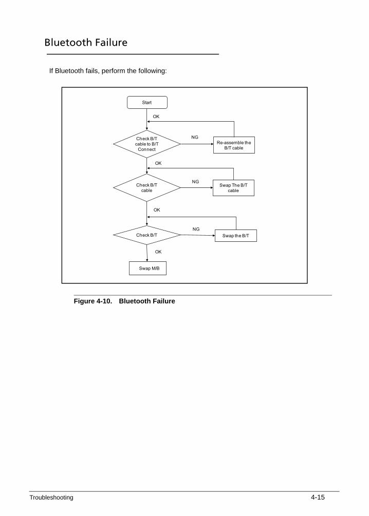
Troubleshooting 4-15
Bluetooth Failure 0
If Bluetooth fails, perform the following:
Figure 4-10. Bluetooth Failure
Start
Check B/T cable to B/T
ConnectRe-assemble the
B/T cable
NG
Check B/T cable
Swap The B/T cable
OK
NG
Swap M/B
Check B/T Swap the B/T
OK
NG
OK
OK

4-16 Troubleshooting
Card Reader Failure 0
If the card reader fails, perform the following:
Figure 4-11. Card Reader Failure
Card read conn well
solder
card read Chip ok
Start
Repair theCard read
conn
SwapM/B card read
Chip
Swap M/B
OK
NG
NG
OK
OK

Troubleshooting 4-17
Thermal Unit Failure 0
If the thermal unit fails, perform the following:
Figure 4-12. Thermal Failure
Start
Connect it well
Replace fan
Insert is well
Replace M/B
Fan cable Well
connected
Fan ok
Thermal well insert
NG
NG
NG
OK
OK
OK
OK

4-18 Troubleshooting
Case Failure 0
If the case fails, perform the following:
Figure 4-13. Case Failure
Start
Connect it well
Replace fan
Insert is well
Replace M/B
Fan cable Well
connected
Fan ok
Thermal well insert
NG
NG
NG
OK
OK
OK
OK

Troubleshooting 4-19
Other Functions Failure 0
HDD Not Operating Correctly 0
To determine if the HDD is operating correctly, perform the following:
1. Disconnect all external devices.
2. Run a complete virus scan using up-to-date software to confirm the computer is virus free.
3. Run the Windows Vista Startup Repair Utility:
a. Insert the Windows Vista Operating System DVD in the ODD and restart the computer.
b. When prompted, press any key to start to the operating system DVD.
c. When the Install Windows screen appears, click Next.
d. Select Repair your computer.
e. When the System Recovery Options screen appears, click Next.
f. Select the appropriate operating system, and click Next.
NOTE:NOTE:Click Load Drivers if controller drives are required.
g. Select Startup Repair.
NOTE:NOTE:Startup Repair attempts to locate and resolve issues with the computer.
h. When complete, click Finish.
If an issue is discovered, follow the on-screen information to resolve the problem.
1. Run the Windows Memory Diagnostic Tool. For more information see Windows Help and Support.
2. Restart the computer and press F2 to enter the BIOS Utility. Check the BIOS settings are correct and that CD/DVD drive is set as the first boot device on the Boot menu.
3. Confirm all cables and jumpers on the HDD and ODD are set correctly.
4. Remove any recently added hardware and associated software.
5. Run the Windows Disk Defragmenter. For more information see Windows Help and Support.
6. Run Windows Check Disk by entering chkdsk /r from a command prompt. For more information see Windows Help and Support.
7. Restore system and file settings from a known good date using System Restore.
8. If the issue is not fixed, repeat the preceding steps and select an earlier time and date.
9. Replace the HDD. (Refer to Maintenance Flowchart)
Mainboard 0
To determine if the mainboard is operating correctly, perform the following:
1. Check component connections to mainboard.
2. To test for mainboard fault, swap mainboard.

4-20 Troubleshooting
ODD Failure 0
If the ODD fails, perform the following:
Figure 4-14. ODD Failure
ODD Not Operating Correctly 0
If the ODD exhibits any of the following symptoms it may be faulty:
Audio CDs do not play when loaded
DVDs do not play when loaded
Blank discs do not burn correctly
DVD or CD play breaks up or jumps
Optical drive not found or not active:
Not shown in My Computer or the BIOS setup
LED does not flash when the computer starts up
The tray does not eject
Access failure screen is shown
The ODD is noisy

Troubleshooting 4-21
Perform the following:
1. Boot the computer and retry the operation.
2. Use an different disc.
3. Navigate to Start Computer. Check that the ODD device is shown in the Devices with Removable Storage panel.
4. Navigate to Start Control Panel System and Maintenance System Device Manager.
5. Double click lDE ATA/ATAPI controllers. If a device shows a down arrow, right click on the device and click Enable.
6. Double-click DVD/CD-ROM drives. If the device shows a down arrow, right click on the device and click Enable.
7. Make sure that there are no yellow exclamation marks against the items in lDE ATA/ATAPI controllers. If a device has an exclamation mark, uninstall and reinstall the driver.
8. Check that there are no yellow exclamation marks against the items in DVD/CD-ROM drives. If a device has an exclamation mark, uninstall and reinstall the driver.
9. If the exclamation marker is not removed from the item in the lists, remove any recently installed software and retrying the operation.
Discs Do Not Play 0
If discs do not play when inserted into the drive, perform the following:
1. Check that the disc is correctly seated in the drive tray and that the label on the disc is visible.
2. Check that the media is clean and scratch free.
3. Try an alternate disc in the drive.
4. Confirm that AutoPlay is enabled:
Navigate to Start Control Panel Hardware and Sound AutoPlay.
Select Use AutoPlay for all media and devices.
In the Audio CD and DVD Movie fields, select the desired player from the drop down menu.
5. Check that the Regional Code is correct for the selected media:
IMPORTANT:?Region can only be changed a limited number of times. After Changes remaining reaches zero, the region cannot be changed even when Windows is reinstalled or the drive is moved to another computer.
Navigate to Start Control Panel System and Maintenance System Device Manager.
Double click DVD/CD-ROM drives.
Right click DVD drive and click Properties, then click the DVD Region tab.
Select the region suitable for the media inserted in the drive.

4-22 Troubleshooting
Discs Do Not Burn Properly 0
If discs can not be burned, perform the following:
6. Confirm that the default drive is record enabled:
Navigate to Start Computer and right-click the writable ODD icon. Click Properties.
Select the Recording tab. In the Desktop disc recording panel, select the writable ODD from the drop down list.
Click OK.
7. Confirm that the software used for burning discs is the factory default. If using different software, refer to the software's user manual.
Playback is Choppy 0
If playback is choppy or jumps, perform the following:
1. Check that system resources are not running low:
Close some applications.
Reboot and try the operation again.
2. Check that the ODD controller transfer mode is set to DMA.
3. Navigate to Start Control Panel System and Maintenance System Device Manager.
4. Double click IDE ATA/ATAPI controllers, then right click ATA Device 0.
5. Click Properties and select the Advanced Settings tab. Make sure the Enable DMA box is checked and click OK.
6. Repeat for each ATA Device shown if applicable.
Drive Not Detected 0
If Windows cannot detect the drive, perform the following:
1. Start the computer and press F2 to enter the BIOS Utility.
2. Verify that the drive is detected in the ATAPI Model Name field on the Information page.
NOTE:NOTE:Verify that the entry is identical to one of the ODDs specified in Specification Tables.
Remove power and remove the cover to inspect the connections to the ODD. (Refer to Maintenance Flowchart)
Check for broken connectors on the drive, motherboard, and cables.
Check for bent or broken pins on the drive, motherboard, and cable connections.
Try an alternate cable, if available. If the drive works with the new cable, the original cable should be replaced.
3. Reseat the drive, making sure and all cables are connected correctly.
4. Replace the ODD. (Refer to Maintenance Flowchart)

Troubleshooting 4-23
Drive Read Failure 0
If discs cannot be read when inserted in the drive, perform the following.
1. Remove and clean the failed disc.
2. Retry reading the CD or DVD.
Test the drive using other discs.
Play a DVD movie
Listen to a music CD
If the ODD works properly with alternate discs, the original disc is probably defective and should be replaced.
3. Remove the power and remove the cover to inspect the connections to the ODD. Refer to Online Support Information.
Check for broken connectors on the drive, motherboard, and cables.
Check for bent or broken pins on the drive, motherboard, and cable connections.
Try a different cable. If the drive works with the new cable, the original cable should be replaced.
4. Replace the ODD. (Refer to Maintenance Flowchart)
Random Loss of BIOS Settings 0
If the computer is experiencing intermittent loss of BIOS information, perform the following:
1. If the computer is more than one year old, replace the CMOS battery.
2. Run a complete virus scan using up to date software to confirm the computer is virus free.
3. If the computer is experiencing HDD or ODD BIOS information loss, disconnect and reconnect the power and data cables between devices.
4. If the BIOS settings are still lost, replace the cables.
5. If HDD information is missing from the BIOS, the drive may be defective and should be replaced.
6. Replace the Motherboard.
7. If the Issue is still not resolved, refer to Online Support Information.
External Mouse Failure 0
If an external Mouse fails, perform the following:
1. Use a different mouse.
2. If the mouse uses a wireless connection, insert new batteries and confirm there is a good connection. Refer to the mouse user manual.
3. If the mouse uses a USB connection, use a different USB port.
4. Use a different program to verify mouse operation. Reinstall the program experiencing mouse failure.
5. Restart the computer.
6. Remove recently added hardware and associated software.
7. Remove recently added software and reboot the computer.
8. Restore system and file settings from a known good date using System Restore.

4-24 Troubleshooting
9. If the issue is resolved, repeat Step 8 and select an earlier time and date.
10. Run the Event Viewer to check the events log for errors. For more information refer to Windows Help and Support.
11. Roll back the mouse driver to the previous version if updated recently.
12. Remove and reinstall the mouse driver.
13. Check the Device Manager to determine that:
The device is properly installed. There are no red Xs or yellow exclamation marks
There are no device conflicts
No hardware is listed under Other Devices
14. If the Issue is still not resolved, refer to Online Support Information.

Troubleshooting 4-25
Intermittent Problems 0
Intermittent system hang problems can be caused by a variety of reasons that have nothing to do with a hardware defect, such as: cosmic radiation, electrostatic discharge, or software errors. FRU replacement should be considered only when a recurring problem exists.
When analyzing an intermittent problem, perform the following:
1. Run the advanced diagnostic test for the system board in loop mode at least 10 times.
2. If no error is detected, do not replace any FRU.
3. If an error is detected, replace the FRU. Rerun the test to verify that there are no more errors.
Undetermined Problems 0
The diagnostic problems does not identify which adapter or device failed, which installed devices are incorrect, whether a short circuit is suspected, or whether the system is inoperative.
Perform the following procedures to isolate the failing FRU (do not isolate non-defective FRU).
NOTE:NOTE:Verify that all attached devices are supported by the computer.
NOTE:NOTE:Verify that the power supply being used at the time of the failure is operating correctly. (Refer to Power On Issues).
1. Remove power from the computer.
2. Visually check them for damage. If any problems are found, replace the FRU.
3. Remove or disconnect all of the following devices:
Non-Acer devices
Printer, mouse, and other external devices
Battery pack
Hard disk drive
DIMM
CD-ROM/Diskette drive Module
PC Cards
4. Apply power to the computer.
5. Determine if the problem has changed.
6. If the problem does not recur, connect the removed devices one at a time until failing FRU is found.
7. If the problem remains, replace the following FRUs one at a time. Do not replace a non-defective FRU:
System board
LCD assembly

4-26 Troubleshooting
Post Codes 0
The following are the InsydeH2O™ Functionality POST code tables. The components of the POST code table includes: SEC phase, PEI phase, DXE phase, BDS phase, CSM functions, S3 functions and ACPI functions.
Table 4-2. POST Code Range
Phase POST Code Range
SEC 0x01 - 0x0F
PEI 0x70 - 0x9F
DXE 0x40 - 0x6F
BDS 0x10 - 0x3F
SMM 0xA0 - 0xBF
S3 0xC0 - 0xCF
ASL 0x51 – 0x55
0xE1 – 0xE4
PostBDS 0xF9 – 0xFE
InsydeH2ODDT™ Reserve 0xD0 – 0xD7
OEM Reserve 0xE8 – 0xEB
Reserved 0xD8 – 0xE0
0xE5 – 0xE7
0xEC – 0xF8
Table 4-3. SEC Phase POST Code Table
Functionality Name (Include\PostCode.h)
Phase Post Code
Description
SEC_SYSTEM_POWER_ON SEC 01 CPU power on and switch to Protected mode
SEC_BEFORE_MICROCODE_PATCH SEC 02 Patching CPU microcode
SEC_AFTER_MICROCODE_PATCH SEC 03 Setup Cache as RAM
SEC_ACCESS_CSR* SEC 04 PCIE MMIO Base Address initial
SEC_GENERIC_MSRINIT* SEC 05 CPU Generic MSR initialization
SEC_CPU_SPEEDCFG* SEC 06 Setup CPU speed
SEC_SETUP_CAR_OK SEC 07 Cache as RAM test

Troubleshooting 4-27
SEC_FORCE_MAX_RATIO* SEC 08 Tune CPU frequency ratio to maximum level
SEC_GO_TO_SECSTARTUP SEC 09 Setup BIOS ROM cache
SEC_GO_TO_PEICORE SEC 0A Enter Boot Firmware Volume
* 3rd party relate functions – Platform dependence.
Table 4-4. PEI Phase POST Code Table
Functionality Name (Include\PostCode.h)
Phase Post Code
Description
PEI_SIO_INIT PEI 70 Super I/O Initialization
PEI_CPU_REG_INIT PEI 71 CPU Early Initialization
PEI_CPU_AP_INIT* PEI 72 Multi-processor Early Initial
PEI_CPU_HT_RESET* PEI 73 HyperTransport Initialization
PEI_PCIE_MMIO_INIT PEI 74 PCIE MMIO BAR Initialization
PEI_NB_REG_INIT PEI 75 North Bridge Early Initialization
PEI_SB_REG_INIT PEI 76 South Bridge Early Initialization
PEI_PCIE_TRAINING* PEI 77 PCIE Training
PEI_TPM_INIT PEI 78 TPM Initialization
PEI_SMBUS_INIT PEI 79 SMBUS Early Initialization
PEI_PROGRAM_CLOCK_GEN PEI 7A Clock Generator Initialization
PEI_IGD_EARLY_INITIAL * PEI 7B Internal Graphic device early Initialization
PEI_HECI_INIT* PEI 7C HECI Initialization
PEI_WATCHDOG_INIT* PEI 7D Watchdog timer Initialization
PEI_MEMORY_INIT PEI 7E Memory Initial for Normal boot.
PEI_MEMORY_INIT_FOR_CRISIS PEI 7F Memory Initial for Crisis Recovery
PEI_MEMORY_INSTALL PEI 80 Simple Memory test
PEI_TXTPEI* PEI 81 TXT function early Initialization
PEI_SWITCH_STACK PEI 82 Start to use Memory
PEI_MEMORY_CALLBACK PEI 83 Set cache for physical memory
Table 4-3. SEC Phase POST Code Table (Continued)
Functionality Name (Include\PostCode.h)
Phase Post Code
Description

4-28 Troubleshooting
PEI_ENTER_RECOVERY_MODE PEI 84 Recovery device Initialization
PEI_RECOVERY_MEDIA_FOUND PEI 85 Found Recovery image
PEI_RECOVERY_MEDIA_NOT_FOUND PEI 86 Recovery image not found
PEI_RECOVERY_LOAD_FILE_DONE PEI 87 Load Recovery Image completed
PEI_RECOVERY_START_FLASH PEI 88 Start Flash BIOS with Recovery image
PEI_ENTER_DXEIPL PEI 89 Loading BIOS image to RAM
PEI_FINDING_DXE_CORE PEI 8A Loading DXE core
PEI_GO_TO_DXE_CORE PEI 8B Enter DXE core
* 3rd party relate functions – Platform dependence.
Table 4-5. DXE Phase POST Code Table
Functionality Name (Include\PostCode.h)
Phase Post Code
Description
DXE_TCGDXE* DXE 40 TPM initial in DXE
DXE_SB_SPI_INIT* DXE 41 South bridge SPI initialization
DXE_CF9_RESET* DXE 42 Setup Reset service
DXE_SB_SERIAL_GPIO_INIT* DXE 43 South bridge Serial GPIO initialization
DXE_SMMACCESS* DXE 44 Setup SMM ACCE SS service
DXE_NB_INIT* DXE 45 North bridge Middle initialization
DXE_SIO_INIT* DXE 46 Super I/O DXE initialization
DXE_LEGACY_REGION* DXE 47 Setup Legacy Region service
DXE_SB_INIT* DXE 48 South Bridge Middle initialization
DXE_IDENTIFY_FLASH_DEVICE DXE 49 Identify Flash device
DXE_FTW_INIT DXE 4A Fault Tolerant Write verification
DXE_VARIABLE_INIT DXE 4B Variable Service initialization
DXE_VARIABLE_INIT_FAIL DXE 4C Fail to initial Variable Service
DXE_MTC_INIT DXE 4D MTC Initial
DXE_CPU_INIT DXE 4E CPU Middle Initialization
Table 4-4. PEI Phase POST Code Table (Continued)
Functionality Name (Include\PostCode.h)
Phase Post Code
Description

Troubleshooting 4-29
DXE_MP_CPU_INIT DXE 4F Multi-processor MiddleInitialization
DXE_SMBUS_INIT DXE 50 SMBUS Driver Initialization
DXE_SMART_TIMER_INIT DXE 51 8259 Initialization
DXE_PCRTC_INIT DXE 52 RTC Initialization
DXE_SATA_INIT* DXE 53 SATA Controller EarlyInitialization
DXE_SMM_CONTROLER_INIT* DXE 54 Setup SMM Control service
DXE_LEGACY_INTERRUPT* DXE 55 Setup Legacy Interrupt service
DXE_RELOCATE_SMBASE DXE 56 Relocate SMM BASE
DXE_FIRST_SMI DXE 57 SMI test
DXE_VTD_INIT* DXE 58 VTD Initial
DXE_BEFORE_CSM16_INIT DXE 59 Legacy BIOS Initialization
DXE_AFTER_CSM16_INIT DXE 5A Legacy interrupt function Initialization
DXE_LOAD_ACPI_TABLE DXE 5B ACPI Table Initialization
DXE_SB_DISPATCH* DXE 5C Setup SB SMM Dispatcher service
DXE_SB_IOTRAP_INIT* DXE 5D Setup SB IOTRAP Service
DXE_SUBCLASS_DRIVER* DXE 5E Build AMT Table
DXE_PPM_INIT* DXE 5F PPM Initialization
DXE_HECIDRV_INIT* DXE 60 HECIDRV Initialization
* 3rd party relate functions – Platform dependence.
Table 4-6. BDS Phase POST Code Table
Functionality Name (Include\PostCode.h) Phase Post Code
Description
BDS_ENTER_BDS BDS 10 Enter BDS entry
BDS_INSTALL_HOTKEY BDS 11 Install Hotkey service
BDS_ASF_INIT* BDS 12 ASF Initialization
BDS_PCI_ENUMERATION_START BDS 13 PCI enumeration
Table 4-5. DXE Phase POST Code Table (Continued)
Functionality Name (Include\PostCode.h)
Phase Post Code
Description

4-30 Troubleshooting
BDS_BEFORE_PCIIO_INSTALL BDS 14 PCI resource assign complete
BDS_PCI_ENUMERATION_END BDS 15 PCI enumeration complete
BDS_CONNECT_CONSOLE_IN BDS 16 Keyboard Controller, keyboard and mouse initialization
BDS_CONNECT_CONSOLE_OUT BDS 17 Video device initialization
BDS_CONNECT_STD_ERR BDS 18 Error report device initialization
BDS_CONNECT_USB_HC BDS 19 USB host controller initialization
BDS_CONNECT_USB_BUS BDS 1A USB BUS driver initialization
BDS_CONNECT_USB_DEVICE BDS 1B USB device driver initialization
BDS_NO_CONSOLE_ACTION BDS 1C Console device initial fail
BDS_DISPLAY_LOGO_SYSTEM_INFO BDS 1D Display logo or system information
BDS_START_IDE_CONTROLLER BDS 1E IDE controller initialization
BDS_START_SATA_CONTROLLER BDS 1F SATA controller initialization
BDS_START_ISA_ACPI_CONTROLLER BDS 20 SIO controller initialization
BDS_START_ISA_BUS BDS 21 ISA BUS driver initialization
BDS_START_ISA_FDD BDS 22 Floppy device initialization
BDS_START_ISA_SEIRAL BDS 23 Serial device initialization
BDS_START_IDE_BUS BDS 24 IDE device initialization
BDS_START_AHCI_BUS BDS 25 AHCI device initialization
BDS_CONNECT_LEGACY_ROM BDS 26 Dispatch option ROMs
BDS_ENUMERATE_ALL_BOOT_OPTION BDS 27 Get boot device information
BDS_END_OF_BOOT_SELECTION BDS 28 End of boot selection
Table 4-6. BDS Phase POST Code Table (Continued)
Functionality Name (Include\PostCode.h) Phase Post Code
Description

Troubleshooting 4-31
BDS_ENTER_SETUP BDS 29 Enter Setup Menu
BDS_ENTER_BOOT_MANAGER BDS 2A Enter Boot manager
BDS_BOOT_DEVICE_SELECT BDS 2B Try to boot system to OS
BDS_EFI64_SHADOW_ALL_LEGACY_ROM BDS 2C Shadow Misc Option ROM
BDS_ACPI_S3SAVE BDS 2D Save S3 resume required data in RAM
BDS_READY_TO_BOOT_EVENT BDS 2E Last Chipset initial before boot to OS
BDS_GO_LEGACY_BOOT BDS 2F Start to boot Legacy OS
BDS_GO_UEFI_BOOT BDS 30 Start to boot UEFI OS
BDS_LEGACY16_PREPARE_TO_BOOT BDS 31 Prepare to Boot to Legacy OS
BDS_EXIT_BOOT_SERVICES* BDS 32 Send END of POST Message to ME via HECI
BDS_LEGACY_BOOT_EVENT BDS 33 Last Chipset initial before boot to Legacy OS.
BDS_ENTER_LEGACY_16_BOOT BDS 34 Ready to Boot Legacy OS.
BDS_RECOVERY_START_FLASH BDS 35 Fast Recovery Start Flash.
* 3rd party relate functions – Platform dependence.
Table 4-7. PostBDS POST Code Table
Functionality Name (Include\PostCode.h) Phase Post Code
Description
POST_BDS_NO_BOOT_DEVICE POST_BDS F9 No Boot Device
POST_BDS_START_IMAGE POST_BDS FB UEFI Boot Start Image
POST_BDS_ENTER_INTI9 POST_BDS FD Legacy 16 boot entry
POST_BDS_BOOT_SECTOR POST_BDS FE Try to Boot with INT 19
Table 4-6. BDS Phase POST Code Table (Continued)
Functionality Name (Include\PostCode.h) Phase Post Code
Description

4-32 Troubleshooting
Table 4-8. S3 Functions POST Code Table
Functionality Name (Include\PostCode.h) Phase Post Code
Description
S3_RESTORE_MEMORY_CONTROLLER PEI C0 Memory initial for S3 resume
S3_INSTALL_S3_MEMORY PEI C1 Get S3 resume required data from memory
S3_SWITCH_STACK PEI C2 Start to use memory during S3 resume
S3_MEMORY_CALLBACK PEI C3 Set cache for physical memory during S3 resume
S3_ENTER_S3_RESUME_PEIM PEI C4 Start to restore system configuration
S3_BEFORE_ACPI_BOOT_SCRIPT PEI C5 Restore system configuration stage1
S3_BEFORE_RUNTIME_BOOT_SCRIPT PEI C6 Restore system configuration stage2
S3_BEFORE_RELOCATE_SMM_BASE PEI C7 Relocate SMM BASE during S3 resume
S3_BEFORE_MP_INIT PEI C8 Multi-processor initial during S3 resume
S3_BEFORE_RESTORE_ACPI_CALLBACK PEI C9 Start to restore system configuration in SMM
S3_AFTER_RESTORE_ACPI_CALLBACK PEI CA Restore system configuration in SMM complete
S3_GO_TO_FACS_WAKING_VECTOR PEI CB Back to OS
Table 4-9. ACPI Functions POST Code Table
Functionality Name (Include\PostCode.h) Phase Post Code
Description
ASL_ENTER_S1 ASL 51 Prepare to enter S1
ASL_ENTER_S3 ASL 53 Prepare to enter S3
ASL_ENTER_S4 ASL 54 Prepare to enter S4
ASL_ENTER_S5 ASL 55 Prepare to enter S5
ASL_WAKEUP_S1 ASL E1 System wakeup from S1
ASL_WAKEUP_S3 ASL E3 System wakeup from S3
ASL_WAKEUP_S4 ASL E4 System wakeup from S4

Troubleshooting 4-33
Table 4-10. SMM Functions POST Code Table
Functionality Name (Include\PostCode.h)
Phase Post Code
Description
SMM_IDENTIFY_FLASH_DEVICE SMM 0xA0 Identify Flash device in SMM
SMM_SMM_PLATFORM_INIT SMM 0xA2 SMM service initial
SMM_ACPI_ENABLE_START SMM 0xA6 OS call ACPI enable function
SMM_ACPI_ENABLE_END SMM 0xA7 ACPI enable function complete
SMM_S1_SLEEP_CALLBACK SMM 0xA1 Enter S1
SMM_S3_SLEEP_CALLBACK SMM 0xA3 Enter S3
SMM_S4_SLEEP_CALLBACK SMM 0xA4 Enter S4
SMM_S5_SLEEP_CALLBACK SMM 0xA5 Enter S5
SMM_ACPI_DISABLE_START SMM 0xA8 OS call ACPI disable function
SMM_ACPI_DISABLE_END SMM 0xA9 ACPI disable function complete
Table 4-11. InsydeH2ODDT Debugger POST Code Table
Functionality Name (Include\PostCode.h) Post Code Description
Used by Insyde debugger 0x0D Waiting for device connect
Used by Insyde debugger 0xD0 Waiting for device connect
Used by Insyde debugger 0xD1 InsydeH2ODDT Ready
Used by Insyde debugger 0xD2 EHCI not found
Used by Insyde debugger 0xD3 Debug port connect low speed device
Used by Insyde debugger 0xD4 DDT Cable become low speed device
Used by Insyde debugger 0xD5 DDT Cable Transmission Error (Get descriptor fail)
Used by Insyde debugger 0xD6 DDT Cable Transmission Error (Set Debug mode fail)
Used by Insyde debugger 0xD7 DDT Cable Transmission Error (Set address fail)

4-34 Troubleshooting

CHAPTER 5
Jumper and Connector Locations

5-2
Mainboard Top . . . . . . . . . . . . . . . . . . . . . . . . . . . . . . . . . . . . . . 5-3Mainboard Bottom . . . . . . . . . . . . . . . . . . . . . . . . . . . . . . . . . . . 5-4Clearing Password and BIOS Recovery . . . . . . . . . . . . . . . . . . . . 5-5
Clearing Password . . . . . . . . . . . . . . . . . . . . . . . . . . . . . . . . . 5-5BIOS Recovery by Crisis Disk. . . . . . . . . . . . . . . . . . . . . . . . . . 5-6

Jumper and Connector Locations 5-3
Jumper and Connector Locations
Mainboard Top 0
Figure 5-1. Mainboard Top
Table 5-1. Mainboard Top
Item Description Item Description
JLED2 Power Sub Board Connector (SJV70)
JHDD1 Main HDD Connector
JLED1 Power Sub Board Connector (JE70)
JBT1 Bluetooth Connector
JLVDS1 LVDS Panel Connector JTP2 Touch Pad Connector (SJV70)
JKB1 Keyboard Connector JBATT1 RTC Battery Connector
JSPK1 Internal Speaker Connector JREAD1 Card Reader Connector
JMIC2 Internal Microphone Connector JHP1 Combo Audio Jack
JLAN1 LAN Sub Board Connector JMIC1 External Microphone Connector
JTP1 Touch Pad Connector (JE70) JUSB2 USB Connector (Right Side)
JODD1 ODD Connector JHDMI1 HDMI Output Connector
JUSB1 USB Sub Board Connector (Left Side)
JCRT1 CRT Output Connector

5-4 Jumper and Connector Locations
Mainboard Bottom 0
Figure 5-2. Mainboard Bottom
Table 5-2. Mainboard Bottom
Item Description Item Description
PJP1 DC-IN Jack Connector JMINI2 Mini PCI-E Connector
PJP2 Battery Connector JDIMM1 DDR3 Memory Socket
JFAN1 FAN Connector JDIMM2 DDR3 Memory Socket
JHDD2 2nd HDD Connector JMINI1 Mini PCI-E Connector
JCPU1 CPU Socket

Jumper and Connector Locations 5-5
Clearing Password and BIOS Recovery 0
This section provides users with the SOP (standard operating procedure) for clearing the BIOS password and recovering the BIOS for the Acer Aspire 7560/7560G.
Clearing Password 0
NOTE:NOTE:The following procedure is only for clearing BIOS Password (Supervisor Password and User Password).
Clearing BIOS Password 0
If a BIOS password (Supervisor Password and/or User Password) is set, the BIOS will prompt for the password at system POST or upon entering the BIOS setup menu. Clear the password check with the following procedure:
1. Remove AC adapter.
2. Locate the RTC reset point and short it (A). (Figure 5-3)
Figure 5-3. CMOS Jumper
3. Plug in AC adapter.
4. Restart the system and press F2 to enter BIOS Utility Setup menu.
5. If no password prompt is shown, BIOS password is cleared.
6. If password prompt is shown, repeat steps 1 through 5.
Table 5-3. CMOS Jumper
Item Description
Clear CMOS Clear CMOS Jumper (RTC reset point)
A

5-6 Jumper and Connector Locations
BIOS Recovery by Crisis Disk 0
BIOS Recovery Boot Block 0
BIOS Recovery Boot Block is a special block of BIOS. It is used to boot up the system with minimum BIOS initialization. Users can enable this feature to restore the BIOS firmware if a previous BIOS flashing process has failed.
BIOS Recovery Hotkey 0
To enable the BIOS Recovery process, use the function hotkey, Fn + Esc, during BIOS POST. The AC adapter and battery are required to be installed during this process.
Steps for BIOS Recovery using USB HDD 0
NOTE:NOTE:Prior to performing the recovery, prepare a Crisis USB key. The Crisis USB key is created by executing the Crisis Disk program in another system with Windows® 7 OS.
Creating a USB Crisis Key 0
1. Plug in USB HDD.
2. Launch Windows Explorer or press < + E>.
3. Right-click on USB HDD. (Figure 5-4)
Figure 5-4. Format Menu
4. Select Format from pop-up menu.

Jumper and Connector Locations 5-7
5. Format USB HDD using the Quick Format option (Figure 5-5).
Figure 5-5. Format USB HDD
6. Click Start to begin the procedure.
7. Click OK to close the warning dialogue (Figure 5-6).
Figure 5-6. Format Warning Dialogue

5-8 Jumper and Connector Locations
8. When formatting is complete, a dialogue is shown. (Figure 5-7)
Figure 5-7. Format Complete Dialogue
9. Click OK to close dialogue.
10. Click Close to close the USB HDD Format dialogue (Figure 5-8).
Figure 5-8. Close Format Dialogue
NOTE:NOTE:A DOS mode flash package is a compressed file (*.zip, *.7z, *.rar). The format of the file name is xxxxxxxx.7z where, ‘x’ is the project code.
11. Unzip the DOS mode flash package to the HDD of the computer.
NOTE:NOTE:A BIOS, or ROM (read-only memory), file is a file with the extension FD (*.fd).
12. Make sure no other BIOS file is saved in the root directory of the USB HDD.
13. Copy the project BIOS file (xxxxxx.fd) to the root directory of the USB HDD.
14. Rename the project BIOS file to BIOS.fd.

Jumper and Connector Locations 5-9
Using the USB Crisis Key 0
1. Turn off the system and disconnect the AC adapter. Refer to Getting Started.
NOTE:NOTE:Make sure the power and charge lights are off, as shown on the power indicator. Refer to Closed Front View.
2. Plug in USB HDD.
3. Press and hold <Fn + ESC>.
4. Plug in the AC adapter.
5. Press the Power button to initiate system CRISIS mode.
NOTE:NOTE:If the CRISIS mode did not initiate correctly, make sure the file name is correct on the USB HDD. Disconnect the AC adapter and battery to reset the embedded status. Repeat steps 1 through 5.
6. When CRISIS is complete, the system auto restarts with a workable BIOS.
7. Update the latest version BIOS for this machine by regular BIOS flashing process.

5-10 Jumper and Connector Locations

CHAPTER 6
Field Replaceable Unit List

6-2
Exploded Diagrams . . . . . . . . . . . . . . . . . . . . . . . . . . . . . . . . . . . 6-4Main Assembly . . . . . . . . . . . . . . . . . . . . . . . . . . . . . . . . . . . . 6-4LCD Assembly . . . . . . . . . . . . . . . . . . . . . . . . . . . . . . . . . . . . . 6-6Lower Cover . . . . . . . . . . . . . . . . . . . . . . . . . . . . . . . . . . . . . . 6-8
FRU List . . . . . . . . . . . . . . . . . . . . . . . . . . . . . . . . . . . . . . . . . . . . . 6-9Screw List . . . . . . . . . . . . . . . . . . . . . . . . . . . . . . . . . . . . . . . . . . . 6-20

FRU List 6-3
FRU List
This chapter provides users with a FRU (Field Replaceable Unit) listing in global configurations for the Acer Aspire 7560/7560G. Refer to this chapter whenever ordering for parts to repair or for RMA (Return Merchandise Authorization).
NOTE:NOTE:When ordering FRU parts, check the most up-to-date information available on the regional web or channel. Part number changes will not be noted on the printed Service Guide. For Acer Authorized Service Providers, the Acer office may have a different part number code from those given in the FRU list of this printed Service Guide. Users MUST use the local FRU list provided by the regional Acer office to order FRU parts for repair and service of customer machines.
NOTE:NOTE:To scrap or to return the defective parts, users should follow the local government ordinance or regulations on how to dispose it properly, or follow the rules set by the regional Acer office on how to return it.

6-4 FRU List
Exploded Diagrams 0
Main Assembly 0
Figure 6-1. Main Assembly Exploded Diagram
8
1
2
3
4
5
6
7

FRU List 6-5
Table 6-1. Main Assembly Exploded Diagram
No. Description P/N
1 Upper Cover 60.RB002.001
2 Mainboard MB.BUX02.001
3 Thermal 60.RKJ02.001
4 Speaker (L+R) 23.RB002.003
5 RJ45 Cable 50.RB002.003
6 LAN Board 55.RB002.005
7 Lower Cover 60.RB002.005
8 Fan 23.RB002.001

6-6 FRU List
LCD Assembly 0
Figure 6-2. LCD Assembly Exploded Diagram
Table 6-2. LCD Assembly Exploded Diagram
No. Description P/N
1 LCD Bezel 60.RB002.012
2 LCD Panel LK.17305.002
1
2
7
3
4
5
6

FRU List 6-7
3 LVDS Cable 50.RB002.008
4 LCD Bracket (R) 33.RB002.004
5 LCD Cover 60.RB002.008
6 LCD Bracket (L) 33.RB002.004
7 CCD 57.RKJ02.001
Table 6-2. LCD Assembly Exploded Diagram (Continued)
No. Description P/N

6-8 FRU List
Lower Cover 0
Figure 6-3. Lower Cover Exploded Diagram
Table 6-3. Lower Cover Exploded Diagram
No. Description P/N
1 HDD Door 60.RB002.006
2 Lower Cover 60.RB002.005
1
2

FRU List 6-9
FRU List 0
Table 6-4. FRU List
Category Description P/N
ADAPTER
Adapter DELTA 65W 19V 1.7x5.5x11 Yellow ADP-65VH BA, LV5, Low profile LED LF
AP.06501.033
Adapter Chicony Power 65W 19V 1.7x5.5x11 Yellow CPA09-A065N1, LV5, low profile LF
AP.0650A.017
Adapter Chicony Power 90W 19V 1.7x5.5x11 Blue A10-090P3A / A090A029L, LV5 low profile LF
AP.0900H.001
BATTERY
Battery SANYO AS10D Li-Ion 3S2P SANYO 6 cell 4400mAh Main COMMON new IC BQ8055
BT.00603.124
Battery SONY AS10D Li-Ion 3S2P SONY 6 cell 4400mAh Main COMMON ID:AS10D41
BT.00604.049
Battery PANASONIC AS10D Li-Ion 3S2P PANASONIC 6 cell 4400mAh Main COMMON ID:AS10D51
BT.00605.062
Battery SAMSUNG AS10D Li-Ion 3S2P SAMSUNG 6 cell 4400mAh Main COMMON ID:AS10D61
BT.00606.008
Battery SIMPLO AS10D Li-Ion 3S2P PANASONIC 6 cell 4400mAh Main COMMON ID:AS10D71
BT.00607.125
Battery SIMPLO AS10D Li-Ion 3S2P LGC 6 cell 4400mAh Main COMMON ID:AS10D73
BT.00607.126
Battery SIMPLO AS10D Li-Ion 3S2P SAMSUNG 6 cell 4400mAh Main COMMON ID:AS10D
BT.00607.127
BOARD
Foxconn Bluetooth BRM 2070 (T77H114.01) BT 3.0 BH.21100.010
Foxconn Bluetooth ATH BU12 BH.21100.011
POWER BOARD 55.RB002.001
USB BOARD 2.0 MOUNT W/ FFC 55.RKJ02.001

6-10 FRU List
LAN BOARD 55.RB002.005
Foxconn Wirelss LAN Atheros HB95BG (HM) T77H121.10
NI.23600.077
Foxconn Wireless LAN Atheros HB97 2x2 BGN (HM) NI.23600.072
Liteon Wireless LAN Atheris HB97 2x2 BGN (HM) WN6603AH
NI.23600.073
Liteon Wireless LAN Realtek 8192SE BGN WN6603LH(2x2 BGN)
NI.23600.065
CABLE
BLUETOOTH CABLE-6PIN 50.RB002.002
RJ45 CABLE 50.RB002.003
TP FFC 50.RB002.004
POWER CORD US 3 PIN 27.TAVV5.001
POWER CORD EU 3 PIN 27.TAVV5.002
POWER CORD AUS 3 PIN 27.TAVV5.003
POWER CORD UK 3 PIN 27.TAVV5.004
POWER CORD CHINA 3 PIN 27.TAVV5.005
POWER CORD SWISS 3 PIN 27.TAVV5.006
POWER CORD ITALIAN 3 PIN 27.TAVV5.007
POWER CORD DENMARK 3 PIN 27.TAVV5.008
POWER CORD JP 3 PIN 27.TAVV5.009
POWER CORD SOUTH AFRICA 3 PIN 27.TAVV5.010
POWER CORD KOREA 3 PIN 27.TAVV5.011
POWER CORD ISRAEL 3 PIN 27.TAVV5.012
POWER CORD INDIA 3 PIN 27.TAVV5.013
POWER CORD TWN 3 PIN 27.TAVV5.014
POWER CORD ARGENTINA 3 PIN 27.APV02.001
Table 6-4. FRU List (Continued)
Category Description P/N

FRU List 6-11
CASE/COVER/BRACKET ASSEMBLY
UPPER CASE IMR-GRAY 60.RB002.001
UPPER CASE IMR-BLUE 60.RB002.003
LOWER CASE 60.RB002.005
HDD DOOR FOR W/O 2ND HDD 60.RB002.006
HDD DOOR FOR W/2ND HDD 60.RB002.007
HDD BRACKET-L 33.RB002.001
HDD BRACKET-R 33.RB002.002
CPU/PROCESSOR
CPU AMD - A4-3300M 1.9G 2M 35W B0 HD6480M KC.33002.A4M
CPU AMD - A6-3400M 1.4G 4M 35W B0 HD6520M KC.34002.A6M
CPU AMD - A8-3500M 1.5G 4M 35W B0 HD6620M KC.35002.A8M
ODD MODULE
ODD BD COMBO MODULE 6M.RKJ02.003
ODD BRACKET 33.RB002.003
ODD BEZEL-BD 42.RB002.001
Table 6-4. FRU List (Continued)
Category Description P/N

6-12 FRU List
ODD PANASONIC BD COMBO 12.7mm Tray DL 4X UJ141AJ LF W/O bezel SATA Zero Power + BUS Encryption
KO.00407.006
ODD PIONEER BD COMBO 12.7mm Tray DL 4X BDC-TD03RT LF W/O bezel 1.01 SATA Zero Power + BUS Encryption (Windows 7)
KO.00405.008
ODD HLDS BD COMBO 12.7mm Tray DL 6X CT30P LF W/O bezel 1.00 SATA HF + 3D + Bus Encryption
KO.0060D.007
ODD MODULE
ODD SUPER-MULTI DRIVE MODULE 6M.RKJ02.002
ODD BRACKET 33.RB002.003
ODD BEZEL-SM 42.RB002.002
ODD TOSHIBA Super-Multi DRIVE 12.7mm Tray DL 8X TS-L633F LF W/O bezel SATA (HF + Windows 7)
KU.00801.040
ODD PLDS Super-Multi DRIVE 12.7mm Tray DL 8X DS-8A5SH LF+HF W/O bezel SATA With TI + Rohm Solution (HF + Windows 7)
KU.0080F.014
ODD HLDS Super-Multi DRIVE 12.7mm Tray DL 8X GT34N LF W/O bezel SATA Zero Power Supported, PCC LD (HF + Windows 7)
KU.0080D.057
HDD/HARD DISK DRIVE
HDD SEAGATE 2.5" 5400rpm 320GB ST9320310AS,9RN132-188, Cameron 320G/P SATA 8MB LF F/W:0001SDM1
KH.32001.019
HDD HGST 2.5" 5400rpm 320GB HTS545032B9A300 Panther B SATA LF F/W:C60F Disk imbalance criteria = 0.014g-cm
KH.32007.008
HDD HGST 2.5" 5400rpm 500GB HTS545050B9A300 Panther B SATA LF F/W:C60F Disk imbalance criteria = 0.014g-cm
KH.50007.010
Table 6-4. FRU List (Continued)
Category Description P/N

FRU List 6-13
HDD WD 2.5" 5400rpm 500GB WD5000BPVT-22HXZT1,ML375_AF, 4K drive SATA 8MB LF+HF F/W:01.01A01
KH.50008.021
HDD TOSHIBA 2.5" 5400rpm 500GB MK5059GSXP, Capricron 3BS, 375G/P SATA 8MB LF+HF F/W:GN003J 4K
KH.50004.003
HDD SEAGATE 2.5" 5400rpm 640GB ST9640320AS,9RN134-189, Cameron, 320G/P SATA 8MB LF F/W:0001SDM1
KH.64001.004
HDD WD 2.5" 5400rpm 640GB WD6400BPVT-22HXZT1, ML375M SATA 8MB LF F/W: 01.01A01
KH.64008.005
HDD TOSHIBA 2.5" 5400rpm 640GB MK6459GSXP, Capricron 3BS, 375G/P SATA 8MB LF+HF F/W:GN003J 4K
KH.64004.003
HDD HGST 2.5" 5400rpm 640GB HTS547564A9E384,Jet B, 375G/P SATA 8MB LF+HF F/W:DA3872
KH.64007.003
HDD WD 2.5" 5400rpm 750GB WD7500BPVT-22HXZT1, ML375M, 4K drive SATA 8MB LF F/W:01.01A01
KH.75008.009
HDD TOSHIBA 2.5" 5400rpm 750GB MK7559GSXP, 375G/P, Capricorn BS, 4K drive SATA 8MB LF+HF F/W:GN003J
KH.75004.001
HDD SEAGATE 2.5" 5400rpm 750GB ST9750423AS,9ZW14G-188, Desaru5, 375G/P. SATA 8MB LF+HF F/W:0001SDM1
KH.75001.011
HDD HGST 2.5" 5400rpm 750GB HTS547575A9E384, Jet B, 375G/P SATA 8MB LF F/W:DA3872
KH.75007.004
KEYBOARD
Keyboard ACER AC7T_A10B AC7T Internal 17 Standard 103KS Black US International Texture
KB.I170A.172
Keyboard ACER AC7T_A10B AC7T Internal 17 Standard 103KS Black Greek Texture
KB.I170A.156
Keyboard ACER AC7T_A10B AC7T Internal 17 Standard 103KS Black Arabic Texture
KB.I170A.147
Keyboard ACER AC7T_A10B AC7T Internal 17 Standard 103KS Black Chinese Texture
KB.I170A.151
Keyboard ACER AC7T_A10B AC7T Internal 17 Standard 103KS Black Russian Texture
KB.I170A.164
Table 6-4. FRU List (Continued)
Category Description P/N

6-14 FRU List
Keyboard ACER AC7T_A10B AC7T Internal 17 Standard 103KS Black US International w/ Hebrew Texture
KB.I170A.173
Keyboard ACER AC7T_A10B AC7T Internal 17 Standard 103KS Black Thailand Texture
KB.I170A.169
Keyboard ACER AC7T_A10B AC7T Internal 17 Standard 104KS Black UK Texture
KB.I170A.171
Keyboard ACER AC7T_A10B AC7T Internal 17 Standard 104KS Black German Texture
KB.I170A.155
Keyboard ACER AC7T_A10B AC7T Internal 17 Standard 104KS Black Swiss/G Texture
KB.I170A.168
Keyboard ACER AC7T_A10B AC7T Internal 17 Standard 104KS Black Belgium Texture
KB.I170A.148
Keyboard ACER AC7T_A10B AC7T Internal 17 Standard 104KS Black Danish Texture
KB.I170A.152
Keyboard ACER AC7T_A10B AC7T Internal 17 Standard 104KS Black Italian Texture
KB.I170A.158
Keyboard ACER AC7T_A10B AC7T Internal 17 Standard 104KS Black French Texture
KB.I170A.154
Keyboard ACER AC7T_A10B AC7T Internal 17 Standard 104KS Black Hungarian Texture
KB.I170A.157
Keyboard ACER AC7T_A10B AC7T Internal 17 Standard 104KS Black Norwegian Texture
KB.I170A.162
Keyboard ACER AC7T_A10B AC7T Internal 17 Standard 104KS Black Portuguese Texture
KB.I170A.163
Keyboard ACER AC7T_A10B AC7T Internal 17 Standard 104KS Black Spanish Texture
KB.I170A.166
Keyboard ACER AC7T_A10B AC7T Internal 17 Standard 104KS Black US w/ Canadian French Texture
KB.I170A.174
Keyboard ACER AC7T_A10B AC7T Internal 17 Standard 104KS Black Turkish Texture
KB.I170A.170
Keyboard ACER AC7T_A10B AC7T Internal 17 Standard 104KS Black Sweden Texture
KB.I170A.167
Keyboard ACER AC7T_A10B AC7T Internal 17 Standard 104KS Black FR/Arabic Texture
KB.I170A.153
Keyboard ACER AC7T_A10B AC7T Internal 17 Standard 104KS Black Nordic Texture
KB.I170A.161
Keyboard ACER AC7T_A10B AC7T Internal 17 Standard 104KS Black SLO/CRO Texture
KB.I170A.165
Table 6-4. FRU List (Continued)
Category Description P/N

FRU List 6-15
Keyboard ACER AC7T_A10B AC7T Internal 17 Standard 104KS Black CZ/SK Texture
KB.I170A.150
Keyboard ACER AC7T_A10B AC7T Internal 17 Standard 104KS Black Brazilian Portuguese Texture
KB.I170A.149
Keyboard ACER AC7T_A10B AC7T Internal 17 Standard 107KS Black Japanese Texture
KB.I170A.159
Keyboard ACER AC7T_A10B AC7T Internal 17 Standard 103KS Black Korean Texture
KB.I170A.160
Keyboard ACER AC7T_A10B AC7T Internal 17 Standard 104KS Black Bulgaria Texture
KB.I170A.288
LCD
ASSY LED LCD MODULE 17.3" WXGA+ Glare W/ ANTENNA*2, CCD 1.3M HD, BLACK
6M.RKJ02.001
LCD COVER IMR-BLACK 60.RB002.008
LCD BEZEL 60.RB002.012
ANTENNA WLAN-MAIN 50.RB002.006
ANTENNA WLAN-AUX 50.RB002.007
LCD CABLE 50.RB002.008
Table 6-4. FRU List (Continued)
Category Description P/N
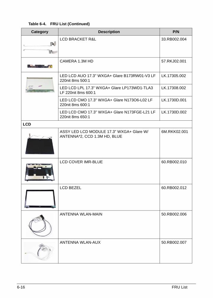
6-16 FRU List
LCD BRACKET R&L 33.RB002.004
CAMERA 1.3M HD 57.RKJ02.001
LED LCD AUO 17.3'' WXGA+ Glare B173RW01-V3 LF 220nit 8ms 500:1
LK.17305.002
LED LCD LPL 17.3" WXGA+ Glare LP173WD1-TLA3 LF 220nit 8ms 600:1
LK.17308.002
LED LCD CMO 17.3" WXGA+ Glare N173O6-L02 LF 220nit 8ms 600:1
LK.1730D.001
LED LCD CMO 17.3'' WXGA+ Glare N173FGE-L21 LF 220nit 8ms 650:1
LK.1730D.002
LCD
ASSY LED LCD MODULE 17.3" WXGA+ Glare W/ ANTENNA*2, CCD 1.3M HD, BLUE
6M.RKK02.001
LCD COVER IMR-BLUE 60.RB002.010
LCD BEZEL 60.RB002.012
ANTENNA WLAN-MAIN 50.RB002.006
ANTENNA WLAN-AUX 50.RB002.007
Table 6-4. FRU List (Continued)
Category Description P/N

FRU List 6-17
LCD CABLE 50.RB002.008
LCD BRACKET R&L 33.RB002.004
CAMERA 1.3M HD 57.RKJ02.001
LED LCD AUO 17.3'' WXGA+ Glare B173RW01-V3 LF 220nit 8ms 500:1
LK.17305.002
LED LCD LPL 17.3" WXGA+ Glare LP173WD1-TLA3 LF 220nit 8ms 600:1
LK.17308.002
LED LCD CMO 17.3" WXGA+ Glare N173O6-L02 LF 220nit 8ms 600:1
LK.1730D.001
LED LCD CMO 17.3'' WXGA+ Glare N173FGE-L21 LF 220nit 8ms 650:1
LK.1730D.002
MAINBOARD
Mainboard ENLS11SB LF UMA MB.BUX02.001
Mainboard ENLS11SB AMD LF Seymour 1G MB.BUZ02.001
Mainboard AS7750G LF SB WHISTLER_PRO+1GB MB.RQF02.001
Mainboard AS7750G LF SB WHISTLER_PRO+2GB MB.RKQ02.001
MEMORY
Memory KINGSTON SO-DIMM DDRIII 1333 1GB ACR128X64D3S1333C9 LF 128*8 0.065um
KN.1GB07.004
Memory UNIFOSA SO-DIMM DDRIII 1333 1GB GU672203EP0200 LF 128*8 0.065um
KN.1GB0H.017
Memory NANYA SO-DIMM DDRIII 1333 1GB NT1GC64BH4B0PS-CG LF 128*16 0.055um
KN.1GB03.034
Memory NANYA SO-DIMM DDRIII 1333 2GB NT2GC64B88B0NS-CG LF 256*8 0.055um
KN.2GB03.021
Table 6-4. FRU List (Continued)
Category Description P/N

6-18 FRU List
Memory ELPIDA SO-DIMM DDRIII 1333 2GB EBJ21UE8BFU0-DJ-F LF 128*8 0.065um
KN.2GB09.009
Memory ELPIDA SO-DIMM DDRIII 1333 2GB EBJ20UF8BCS0-DJ-F LF 256*8 46nm
KN.2GB09.010
Memory KINGSTON SO-DIMM DDRIII 1333 2GB ACR256X64D3S1333C9 LF 128*8 0.065um
KN.2GB07.004
Memory HYNIX SO-DIMM DDRIII 1333 2GB HMT325S6BFR8C-H9 LF 256*8 46nm
KN.2GB0G.018
Memory MICRON SO-DIMM DDRIII 1333 2GB MT8JSF25664HZ-1G4D1 LF 256*8 0.055um
KN.2GB04.017
Memory SAMSUNG SO-DIMM DDRIII 1333 2GB M471B5773DH0-CH9 LF 256*8
KN.2GB0B.030
Memory HYNIX SO-DIMM DDRIII 1333 4GB HMT351S6AFR8C-H9 LF 256*8 0.055um
KN.4GB0G.003
Memory SAMSUNG SO-DIMM DDRIII 1333 4GB M471B5273DH0-CH9 LF 256*8 35nm
KN.4GB0B.015
HEATSINK
FAN 23.RB002.001
THERMAL MODULE UMA WO FAN 60.RKJ02.001
THERMAL MODULE 35W SEY & WHI WO FAN 60.RKN02.001
SPEAKER
MIC SET 23.RB002.002
SPEAKER L+R 23.RB002.003
Table 6-4. FRU List (Continued)
Category Description P/N

FRU List 6-19
MISCELLANEOUS
HDD MYLAR 47.RB002.001
LCD SCREW PAD 47.RB002.002
Table 6-4. FRU List (Continued)
Category Description P/N

6-20 FRU List
Screw List 0
Table 6-5. Screw List
Category Description P/N
SCREW
SCREW 1.98D 3.0L K 4.6D 0.8T ZK NL 86.RB002.001
SCREW 2.5D 5L K 5.5D ZK NL CR3 86.RB002.002
SCREW 2.5D 6L K 5.5D NI NL 86.RB002.003
SCREW 2.5D 3.0L K 5.3D NI NL 86.RB002.004
SCREW M2.5X6 (NL) 86.RB002.005
SCREW 2D 5L K 4.6D ZK NL CR3 86.RB002.006
SCREW 2.5D 3.2L K 6D NI 86.RB002.007
SCREW 2D 3L K 8D ZK NL 86.RB002.008
SCREW 3.0D 3.0L K 4.9D NI 86.RB002.009
SCREW 2.5D 2.3+2L K 5.5D ZK NL1.0T 86.RB002.010

CHAPTER 7
Model Definition and Configuration

7-2
Aspire 7560. . . . . . . . . . . . . . . . . . . . . . . . . . . . . . . . . . . . . . . . . . 7-3Aspire 7560G . . . . . . . . . . . . . . . . . . . . . . . . . . . . . . . . . . . . . . . . 7-13

Model Definition and Configuration 7-3
Model Definition and Configuration
Aspire 7560 0
Table 7-1. RO & Description
Model Country P/N RO Description
AS7560-4333G32Mnkk DK LX.RKJ02.013 EMEA AS7560-4333G32Mnkk W7HP64ASDK2 MC UMACkk_3J 1G+2G/320/6L2.2/5R/CB_bgn_1.3HD_GEk_ENS1SP1
AS7560-4334G32Mnkk DE LX.RKJ02.001 EMEA AS7560-4334G32Mnkk W7HP64ASDE1 MC UMACkk_3J 2*2G/320/6L2.2/5R/CB_bgn_1.3HD_GEk_DE11SP1
AS7560-4334G50Mnbb AL/MK LX.RKK02.001 EMEA AS7560-4334G50Mnbb W7HP64ASAL1 MC UMACbb_3J 2*2G/500_L/BT/6L2.2/5R/CB_bgn_1.3HD_GEb_A111SP1
AS7560-4334G50Mnbb AL/MK LX.RKK0C.001 EMEA AS7560-4334G50Mnbb LINPUSAAL1 UMACbb_3J 2*2G/500_L/BT/6L2.2/5R/CB_bgn_1.3HD_GEb_A111
AS7560-4334G50Mnbb RS/BA LX.RKK02.002 EMEA AS7560-4334G50Mnbb W7HP64ASBA1 MC UMACbb_3J 2*2G/500/BT/6L2.2/5R/CB_bgn_1.3HD_GEb_A151SP1
AS7560-4334G50Mnbb RS/BA LX.RKK0C.002 EMEA AS7560-4334G50Mnbb LINPUSABA1 UMACbb_3J 2*2G/500_L/BT/6L2.2/5R/CB_bgn_1.3HD_GEb_A141
AS7560-4334G50Mnbb SI/HR LX.RKK02.003 EMEA AS7560-4334G50Mnbb W7HP64ASSI1 MC UMACbb_3J 2*2G/500/BT/6L2.2/5R/CB_bgn_1.3HD_GEb_SL11SP1
AS7560-4334G50Mnbb SI/HR LX.RKK0C.003 EMEA AS7560-4334G50Mnbb LINPUSASI1 UMACbb_3J 2*2G/500_L/BT/6L2.2/5R/CB_bgn_1.3HD_GEb_ENQ1

7-4 Model Definition and Configuration
AS7560-4334G50Mnkk AL/MK LX.RKJ02.009 EMEA AS7560-4334G50Mnkk W7HP64ASAL1 MC UMACkk_3J 2*2G/500_L/BT/6L2.2/5R/CB_bgn_1.3HD_GEk_A111SP1
AS7560-4334G50Mnkk AL/MK LX.RKJ0C.005 EMEA AS7560-4334G50Mnkk LINPUSAAL1 UMACkk_3J 2*2G/500_L/BT/6L2.2/5R/CB_bgn_1.3HD_GEk_A111
AS7560-4334G50Mnkk RS/BA LX.RKJ02.010 EMEA AS7560-4334G50Mnkk W7HP64ASBA1 MC UMACkk_3J 2*2G/500/BT/6L2.2/5R/CB_bgn_1.3HD_GEk_A151SP1
AS7560-4334G50Mnkk RS/BA LX.RKJ0C.006 EMEA AS7560-4334G50Mnkk LINPUSABA1 UMACkk_3J 2*2G/500_L/BT/6L2.2/5R/CB_bgn_1.3HD_GEk_A141
AS7560-4334G50Mnkk SI/HR LX.RKJ02.011 EMEA AS7560-4334G50Mnkk W7HP64ASSI1 MC UMACkk_3J 2*2G/500/BT/6L2.2/5R/CB_bgn_1.3HD_GEk_SL11SP1
AS7560-4334G50Mnkk SI/HR LX.RKJ0C.007 EMEA AS7560-4334G50Mnkk LINPUSASI1 UMACkk_3J 2*2G/500_L/BT/6L2.2/5R/CB_bgn_1.3HD_GEk_ENQ1
AS7560-4334G50Mnkk CH LX.RKJ02.016 EMEA AS7560-4334G50Mnkk W7HP64ASCH1 MC UMACkk_3J 2*2G/500_L/6L2.2/5R/CB_bgn_1.3HD_GEk_IT41SP1
AS7560-6344G50Mnkk AL/MK LX.RKJ02.006 EMEA AS7560-6344G50Mnkk W7HP64ASAL1 MC UMACkk_3J 2*2G/500_L/BT/6L2.2/5R/CB_bgn_1.3HD_GEk_A111SP1
AS7560-6344G50Mnkk DK LX.RKJ02.014 EMEA AS7560-6344G50Mnkk W7HP64ASDK2 MC UMACkk_3J 2*2G/500_L/6L2.2/5R/CB_bgn_1.3HD_GEk_ENS1SP1
Table 7-1. RO & Description (Continued)
Model Country P/N RO Description

Model Definition and Configuration 7-5
AS7560-6344G50Mnkk RS/BA LX.RKJ02.007 EMEA AS7560-6344G50Mnkk W7HP64ASBA1 MC UMACkk_3J 2*2G/500/BT/6L2.2/5R/CB_bgn_1.3HD_GEk_A151SP1
AS7560-6344G50Mnkk SI/HR LX.RKJ02.008 EMEA AS7560-6344G50Mnkk W7HP64ASSI1 MC UMACkk_3J 2*2G/500/BT/6L2.2/5R/CB_bgn_1.3HD_GEk_SL11SP1
AS7560-6344G50Mnkk CH LX.RKJ02.015 EMEA AS7560-6344G50Mnkk W7HP64ASCH1 MC UMACkk_3J 2*2G/500_L/6L2.2/5R/CB_bgn_1.3HD_GEk_IT41SP1
AS7560-6344G50Mnkk UA LX.RKJ0C.001 EMEA AS7560-6344G50Mnkk LINPUSAUK1 UMACkk_3J 2*2G/500_L/6L2.2/5R/CB_bgn_1.3HD_GEk_EN71
AS7560-6344G75Mnkk DE LX.RKJ02.002 EMEA AS7560-6344G75Mnkk W7HP64ASDE1 MC UMACkk_3J 2*2G/750/6L2.2/5R/CB_bgn_1.3HD_GEk_DE11SP1
AS7560-8358G75Mnkk CA LX.RKJ02.012 PA AS7560-8358G75Mnkk W7HP64ASCA2 MC UMACkk_3J 2*4G/750/BT/6L2.2/5R/CB_bgn_1.3HD_GEk_FR86SP1
AS7560-E234G50Mnkk AL/MK LX.RKJ02.003 EMEA AS7560-E234G50Mnkk W7HP64ASAL1 MC UMACkk_3J 2*2G/500_L/BT/6L2.2/5R/CB_bgn_1.3HD_GEk_A111SP1
AS7560-E234G50Mnkk AL/MK LX.RKJ0C.002 EMEA AS7560-E234G50Mnkk LINPUSAAL1 UMACkk_3J 2*2G/500_L/BT/6L2.2/5R/CB_bgn_1.3HD_GEk_A111
AS7560-E234G50Mnkk RS/BA LX.RKJ02.004 EMEA AS7560-E234G50Mnkk W7HP64ASBA1 MC UMACkk_3J 2*2G/500/BT/6L2.2/5R/CB_bgn_1.3HD_GEk_A151SP1
Table 7-1. RO & Description (Continued)
Model Country P/N RO Description

7-6 Model Definition and Configuration
AS7560-E234G50Mnkk RS/BA LX.RKJ0C.003 EMEA AS7560-E234G50Mnkk LINPUSABA1 UMACkk_3J 2*2G/500_L/BT/6L2.2/5R/CB_bgn_1.3HD_GEk_A141
AS7560-E234G50Mnkk SI/HR LX.RKJ02.005 EMEA AS7560-E234G50Mnkk W7HP64ASSI1 MC UMACkk_3J 2*2G/500/BT/6L2.2/5R/CB_bgn_1.3HD_GEk_SL11SP1
AS7560-E234G50Mnkk SI/HR LX.RKJ0C.004 EMEA AS7560-E234G50Mnkk LINPUSASI1 UMACkk_3J 2*2G/500_L/BT/6L2.2/5R/CB_bgn_1.3HD_GEk_ENQ1
Table 7-2. CPU, VGA Chip & VRAM 1
Model Country P/N CPU VGA Chip VRAM 1
AS7560-4333G32Mnkk DK LX.RKJ02.013 A43300M UMA N
AS7560-4334G32Mnkk DE LX.RKJ02.001 A43300M UMA N
AS7560-4334G50Mnbb AL/MK LX.RKK02.001 A43300M UMA N
AS7560-4334G50Mnbb AL/MK LX.RKK0C.001 A43300M UMA N
AS7560-4334G50Mnbb RS/BA LX.RKK02.002 A43300M UMA N
AS7560-4334G50Mnbb RS/BA LX.RKK0C.002 A43300M UMA N
AS7560-4334G50Mnbb SI/HR LX.RKK02.003 A43300M UMA N
AS7560-4334G50Mnbb SI/HR LX.RKK0C.003 A43300M UMA N
AS7560-4334G50Mnkk AL/MK LX.RKJ02.009 A43300M UMA N
AS7560-4334G50Mnkk AL/MK LX.RKJ0C.005 A43300M UMA N
AS7560-4334G50Mnkk RS/BA LX.RKJ02.010 A43300M UMA N
AS7560-4334G50Mnkk RS/BA LX.RKJ0C.006 A43300M UMA N
AS7560-4334G50Mnkk SI/HR LX.RKJ02.011 A43300M UMA N
AS7560-4334G50Mnkk SI/HR LX.RKJ0C.007 A43300M UMA N
AS7560-4334G50Mnkk CH LX.RKJ02.016 A43300M UMA N
AS7560-6344G50Mnkk AL/MK LX.RKJ02.006 A63400M UMA N
AS7560-6344G50Mnkk DK LX.RKJ02.014 A63400M UMA N
AS7560-6344G50Mnkk RS/BA LX.RKJ02.007 A63400M UMA N
AS7560-6344G50Mnkk SI/HR LX.RKJ02.008 A63400M UMA N
AS7560-6344G50Mnkk CH LX.RKJ02.015 A63400M UMA N
Table 7-1. RO & Description (Continued)
Model Country P/N RO Description

Model Definition and Configuration 7-7
AS7560-6344G50Mnkk UA LX.RKJ0C.001 A63400M UMA N
AS7560-6344G75Mnkk DE LX.RKJ02.002 A63400M UMA N
AS7560-8358G75Mnkk CA LX.RKJ02.012 A83500M UMA N
AS7560-E234G50Mnkk AL/MK LX.RKJ02.003 E23000M UMA N
AS7560-E234G50Mnkk AL/MK LX.RKJ0C.002 E23000M UMA N
AS7560-E234G50Mnkk RS/BA LX.RKJ02.004 E23000M UMA N
AS7560-E234G50Mnkk RS/BA LX.RKJ0C.003 E23000M UMA N
AS7560-E234G50Mnkk SI/HR LX.RKJ02.005 E23000M UMA N
AS7560-E234G50Mnkk SI/HR LX.RKJ0C.004 E23000M UMA N
Table 7-3. Memory 1 & Memory 2
Model Country P/N Memory 1 Memory 2
AS7560-4333G32Mnkk DK LX.RKJ02.013 SO1GBIII10 SO2GBIII10
AS7560-4334G32Mnkk DE LX.RKJ02.001 SO2GBIII10 SO2GBIII10
AS7560-4334G50Mnbb AL/MK LX.RKK02.001 SO2GBIII10 SO2GBIII10
AS7560-4334G50Mnbb AL/MK LX.RKK0C.001 SO2GBIII10 SO2GBIII10
AS7560-4334G50Mnbb RS/BA LX.RKK02.002 SO2GBIII10 SO2GBIII10
AS7560-4334G50Mnbb RS/BA LX.RKK0C.002 SO2GBIII10 SO2GBIII10
AS7560-4334G50Mnbb SI/HR LX.RKK02.003 SO2GBIII10 SO2GBIII10
AS7560-4334G50Mnbb SI/HR LX.RKK0C.003 SO2GBIII10 SO2GBIII10
AS7560-4334G50Mnkk AL/MK LX.RKJ02.009 SO2GBIII10 SO2GBIII10
AS7560-4334G50Mnkk AL/MK LX.RKJ0C.005 SO2GBIII10 SO2GBIII10
AS7560-4334G50Mnkk RS/BA LX.RKJ02.010 SO2GBIII10 SO2GBIII10
AS7560-4334G50Mnkk RS/BA LX.RKJ0C.006 SO2GBIII10 SO2GBIII10
AS7560-4334G50Mnkk SI/HR LX.RKJ02.011 SO2GBIII10 SO2GBIII10
AS7560-4334G50Mnkk SI/HR LX.RKJ0C.007 SO2GBIII10 SO2GBIII10
AS7560-4334G50Mnkk CH LX.RKJ02.016 SO2GBIII10 SO2GBIII10
AS7560-6344G50Mnkk AL/MK LX.RKJ02.006 SO2GBIII10 SO2GBIII10
AS7560-6344G50Mnkk DK LX.RKJ02.014 SO2GBIII10 SO2GBIII10
AS7560-6344G50Mnkk RS/BA LX.RKJ02.007 SO2GBIII10 SO2GBIII10
AS7560-6344G50Mnkk SI/HR LX.RKJ02.008 SO2GBIII10 SO2GBIII10
AS7560-6344G50Mnkk CH LX.RKJ02.015 SO2GBIII10 SO2GBIII10
Table 7-2. CPU, VGA Chip & VRAM 1 (Continued)
Model Country P/N CPU VGA Chip VRAM 1

7-8 Model Definition and Configuration
AS7560-6344G50Mnkk UA LX.RKJ0C.001 SO2GBIII10 SO2GBIII10
AS7560-6344G75Mnkk DE LX.RKJ02.002 SO2GBIII10 SO2GBIII10
AS7560-8358G75Mnkk CA LX.RKJ02.012 SO4GBIII10 SO4GBIII10
AS7560-E234G50Mnkk AL/MK LX.RKJ02.003 SO2GBIII10 SO2GBIII10
AS7560-E234G50Mnkk AL/MK LX.RKJ0C.002 SO2GBIII10 SO2GBIII10
AS7560-E234G50Mnkk RS/BA LX.RKJ02.004 SO2GBIII10 SO2GBIII10
AS7560-E234G50Mnkk RS/BA LX.RKJ0C.003 SO2GBIII10 SO2GBIII10
AS7560-E234G50Mnkk SI/HR LX.RKJ02.005 SO2GBIII10 SO2GBIII10
AS7560-E234G50Mnkk SI/HR LX.RKJ0C.004 SO2GBIII10 SO2GBIII10
Table 7-4. HDD 1 & HDD 2
Model Country P/N HDD 1(GB) HDD 2(GB)
AS7560-4333G32Mnkk DK LX.RKJ02.013 N320GB5.4KS_4K N
AS7560-4334G32Mnkk DE LX.RKJ02.001 N320GB5.4KS_4K N
AS7560-4334G50Mnbb AL/MK LX.RKK02.001 N500GB5.4KS_4K N
AS7560-4334G50Mnbb AL/MK LX.RKK0C.001 N500GB5.4KS N
AS7560-4334G50Mnbb RS/BA LX.RKK02.002 N500GB5.4KS_4K N
AS7560-4334G50Mnbb RS/BA LX.RKK0C.002 N500GB5.4KS N
AS7560-4334G50Mnbb SI/HR LX.RKK02.003 N500GB5.4KS_4K N
AS7560-4334G50Mnbb SI/HR LX.RKK0C.003 N500GB5.4KS N
AS7560-4334G50Mnkk AL/MK LX.RKJ02.009 N500GB5.4KS_4K N
AS7560-4334G50Mnkk AL/MK LX.RKJ0C.005 N500GB5.4KS N
AS7560-4334G50Mnkk RS/BA LX.RKJ02.010 N500GB5.4KS_4K N
AS7560-4334G50Mnkk RS/BA LX.RKJ0C.006 N500GB5.4KS N
AS7560-4334G50Mnkk SI/HR LX.RKJ02.011 N500GB5.4KS_4K N
AS7560-4334G50Mnkk SI/HR LX.RKJ0C.007 N500GB5.4KS N
AS7560-4334G50Mnkk CH LX.RKJ02.016 N500GB5.4KS_4K N
AS7560-6344G50Mnkk AL/MK LX.RKJ02.006 N500GB5.4KS_4K N
AS7560-6344G50Mnkk DK LX.RKJ02.014 N500GB5.4KS_4K N
AS7560-6344G50Mnkk RS/BA LX.RKJ02.007 N500GB5.4KS_4K N
AS7560-6344G50Mnkk SI/HR LX.RKJ02.008 N500GB5.4KS_4K N
AS7560-6344G50Mnkk CH LX.RKJ02.015 N500GB5.4KS_4K N
Table 7-3. Memory 1 & Memory 2 (Continued)
Model Country P/N Memory 1 Memory 2

Model Definition and Configuration 7-9
AS7560-6344G50Mnkk UA LX.RKJ0C.001 N500GB5.4KS N
AS7560-6344G75Mnkk DE LX.RKJ02.002 N750GB5.4KS_4K N
AS7560-8358G75Mnkk CA LX.RKJ02.012 N750GB5.4KS_4K N
AS7560-E234G50Mnkk AL/MK LX.RKJ02.003 N500GB5.4KS_4K N
AS7560-E234G50Mnkk AL/MK LX.RKJ0C.002 N500GB5.4KS N
AS7560-E234G50Mnkk RS/BA LX.RKJ02.004 N500GB5.4KS_4K N
AS7560-E234G50Mnkk RS/BA LX.RKJ0C.003 N500GB5.4KS N
AS7560-E234G50Mnkk SI/HR LX.RKJ02.005 N500GB5.4KS_4K N
AS7560-E234G50Mnkk SI/HR LX.RKJ0C.004 N500GB5.4KS N
Table 7-5. ODD & Wireless LAN1
Model Country P/N ODD Wireless LAN1
AS7560-4333G32Mnkk DK LX.RKJ02.013 NSM8XS 3rd WiFi 2x2 BGN
AS7560-4334G32Mnkk DE LX.RKJ02.001 NSM8XS 3rd WiFi 2x2 BGN
AS7560-4334G50Mnbb AL/MK LX.RKK02.001 NSM8XS 3rd WiFi 2x2 BGN
AS7560-4334G50Mnbb AL/MK LX.RKK0C.001 NSM8XS 3rd WiFi 2x2 BGN
AS7560-4334G50Mnbb RS/BA LX.RKK02.002 NSM8XS 3rd WiFi 2x2 BGN
AS7560-4334G50Mnbb RS/BA LX.RKK0C.002 NSM8XS 3rd WiFi 2x2 BGN
AS7560-4334G50Mnbb SI/HR LX.RKK02.003 NSM8XS 3rd WiFi 2x2 BGN
AS7560-4334G50Mnbb SI/HR LX.RKK0C.003 NSM8XS 3rd WiFi 2x2 BGN
AS7560-4334G50Mnkk AL/MK LX.RKJ02.009 NSM8XS 3rd WiFi 2x2 BGN
AS7560-4334G50Mnkk AL/MK LX.RKJ0C.005 NSM8XS 3rd WiFi 2x2 BGN
AS7560-4334G50Mnkk RS/BA LX.RKJ02.010 NSM8XS 3rd WiFi 2x2 BGN
AS7560-4334G50Mnkk RS/BA LX.RKJ0C.006 NSM8XS 3rd WiFi 2x2 BGN
AS7560-4334G50Mnkk SI/HR LX.RKJ02.011 NSM8XS 3rd WiFi 2x2 BGN
AS7560-4334G50Mnkk SI/HR LX.RKJ0C.007 NSM8XS 3rd WiFi 2x2 BGN
AS7560-4334G50Mnkk CH LX.RKJ02.016 NSM8XS 3rd WiFi 2x2 BGN
AS7560-6344G50Mnkk AL/MK LX.RKJ02.006 NSM8XS 3rd WiFi 2x2 BGN
AS7560-6344G50Mnkk DK LX.RKJ02.014 NSM8XS 3rd WiFi 2x2 BGN
AS7560-6344G50Mnkk RS/BA LX.RKJ02.007 NSM8XS 3rd WiFi 2x2 BGN
AS7560-6344G50Mnkk SI/HR LX.RKJ02.008 NSM8XS 3rd WiFi 2x2 BGN
AS7560-6344G50Mnkk CH LX.RKJ02.015 NSM8XS 3rd WiFi 2x2 BGN
Table 7-4. HDD 1 & HDD 2 (Continued)
Model Country P/N HDD 1(GB) HDD 2(GB)

7-10 Model Definition and Configuration
AS7560-6344G50Mnkk UA LX.RKJ0C.001 NSM8XS 3rd WiFi 2x2 BGN
AS7560-6344G75Mnkk DE LX.RKJ02.002 NSM8XS 3rd WiFi 2x2 BGN
AS7560-8358G75Mnkk CA LX.RKJ02.012 NSM8XS 3rd WiFi 2x2 BGN
AS7560-E234G50Mnkk AL/MK LX.RKJ02.003 NSM8XS 3rd WiFi 2x2 BGN
AS7560-E234G50Mnkk AL/MK LX.RKJ0C.002 NSM8XS 3rd WiFi 2x2 BGN
AS7560-E234G50Mnkk RS/BA LX.RKJ02.004 NSM8XS 3rd WiFi 2x2 BGN
AS7560-E234G50Mnkk RS/BA LX.RKJ0C.003 NSM8XS 3rd WiFi 2x2 BGN
AS7560-E234G50Mnkk SI/HR LX.RKJ02.005 NSM8XS 3rd WiFi 2x2 BGN
AS7560-E234G50Mnkk SI/HR LX.RKJ0C.004 NSM8XS 3rd WiFi 2x2 BGN
Table 7-6. Bluetooth & NB Chipset
Model Country P/N Bluetooth NB Chipset
AS7560-4333G32Mnkk DK LX.RKJ02.013 N AMD A60M FCH
AS7560-4334G32Mnkk DE LX.RKJ02.001 N AMD A60M FCH
AS7560-4334G50Mnbb AL/MK LX.RKK02.001 BT 3.0 AMD A60M FCH
AS7560-4334G50Mnbb AL/MK LX.RKK0C.001 BT 2.1 AMD A60M FCH
AS7560-4334G50Mnbb RS/BA LX.RKK02.002 BT 3.0 AMD A60M FCH
AS7560-4334G50Mnbb RS/BA LX.RKK0C.002 BT 2.1 AMD A60M FCH
AS7560-4334G50Mnbb SI/HR LX.RKK02.003 BT 3.0 AMD A60M FCH
AS7560-4334G50Mnbb SI/HR LX.RKK0C.003 BT 2.1 AMD A60M FCH
AS7560-4334G50Mnkk AL/MK LX.RKJ02.009 BT 3.0 AMD A60M FCH
AS7560-4334G50Mnkk AL/MK LX.RKJ0C.005 BT 2.1 AMD A60M FCH
AS7560-4334G50Mnkk RS/BA LX.RKJ02.010 BT 3.0 AMD A60M FCH
AS7560-4334G50Mnkk RS/BA LX.RKJ0C.006 BT 2.1 AMD A60M FCH
AS7560-4334G50Mnkk SI/HR LX.RKJ02.011 BT 3.0 AMD A60M FCH
AS7560-4334G50Mnkk SI/HR LX.RKJ0C.007 BT 2.1 AMD A60M FCH
AS7560-4334G50Mnkk CH LX.RKJ02.016 N AMD A60M FCH
AS7560-6344G50Mnkk AL/MK LX.RKJ02.006 BT 3.0 AMD A60M FCH
AS7560-6344G50Mnkk DK LX.RKJ02.014 N AMD A60M FCH
AS7560-6344G50Mnkk RS/BA LX.RKJ02.007 BT 3.0 AMD A60M FCH
AS7560-6344G50Mnkk SI/HR LX.RKJ02.008 BT 3.0 AMD A60M FCH
AS7560-6344G50Mnkk CH LX.RKJ02.015 N AMD A60M FCH
Table 7-5. ODD & Wireless LAN1 (Continued)
Model Country P/N ODD Wireless LAN1

Model Definition and Configuration 7-11
AS7560-6344G50Mnkk UA LX.RKJ0C.001 N AMD A60M FCH
AS7560-6344G75Mnkk DE LX.RKJ02.002 N AMD A60M FCH
AS7560-8358G75Mnkk CA LX.RKJ02.012 BT 3.0 AMD A60M FCH
AS7560-E234G50Mnkk AL/MK LX.RKJ02.003 BT 3.0 AMD A60M FCH
AS7560-E234G50Mnkk AL/MK LX.RKJ0C.002 BT 2.1 AMD A60M FCH
AS7560-E234G50Mnkk RS/BA LX.RKJ02.004 BT 3.0 AMD A60M FCH
AS7560-E234G50Mnkk RS/BA LX.RKJ0C.003 BT 2.1 AMD A60M FCH
AS7560-E234G50Mnkk SI/HR LX.RKJ02.005 BT 3.0 AMD A60M FCH
AS7560-E234G50Mnkk SI/HR LX.RKJ0C.004 BT 2.1 AMD A60M FCH
Table 7-7. Battery & Adapter
Model Country P/N Battery Adapter
AS7560-4333G32Mnkk DK LX.RKJ02.013 6CELL2.2 65W
AS7560-4334G32Mnkk DE LX.RKJ02.001 6CELL2.2 65W
AS7560-4334G50Mnbb AL/MK LX.RKK02.001 6CELL2.2 65W
AS7560-4334G50Mnbb AL/MK LX.RKK0C.001 6CELL2.2 65W
AS7560-4334G50Mnbb RS/BA LX.RKK02.002 6CELL2.2 65W
AS7560-4334G50Mnbb RS/BA LX.RKK0C.002 6CELL2.2 65W
AS7560-4334G50Mnbb SI/HR LX.RKK02.003 6CELL2.2 65W
AS7560-4334G50Mnbb SI/HR LX.RKK0C.003 6CELL2.2 65W
AS7560-4334G50Mnkk AL/MK LX.RKJ02.009 6CELL2.2 65W
AS7560-4334G50Mnkk AL/MK LX.RKJ0C.005 6CELL2.2 65W
AS7560-4334G50Mnkk RS/BA LX.RKJ02.010 6CELL2.2 65W
AS7560-4334G50Mnkk RS/BA LX.RKJ0C.006 6CELL2.2 65W
AS7560-4334G50Mnkk SI/HR LX.RKJ02.011 6CELL2.2 65W
AS7560-4334G50Mnkk SI/HR LX.RKJ0C.007 6CELL2.2 65W
AS7560-4334G50Mnkk CH LX.RKJ02.016 6CELL2.2 65W
AS7560-6344G50Mnkk AL/MK LX.RKJ02.006 6CELL2.2 65W
AS7560-6344G50Mnkk DK LX.RKJ02.014 6CELL2.2 65W
AS7560-6344G50Mnkk RS/BA LX.RKJ02.007 6CELL2.2 65W
AS7560-6344G50Mnkk SI/HR LX.RKJ02.008 6CELL2.2 65W
AS7560-6344G50Mnkk CH LX.RKJ02.015 6CELL2.2 65W
Table 7-6. Bluetooth & NB Chipset (Continued)
Model Country P/N Bluetooth NB Chipset

7-12 Model Definition and Configuration
AS7560-6344G50Mnkk UA LX.RKJ0C.001 6CELL2.2 65W
AS7560-6344G75Mnkk DE LX.RKJ02.002 6CELL2.2 65W
AS7560-8358G75Mnkk CA LX.RKJ02.012 6CELL2.2 65W
AS7560-E234G50Mnkk AL/MK LX.RKJ02.003 6CELL2.2 65W
AS7560-E234G50Mnkk AL/MK LX.RKJ0C.002 6CELL2.2 65W
AS7560-E234G50Mnkk RS/BA LX.RKJ02.004 6CELL2.2 65W
AS7560-E234G50Mnkk RS/BA LX.RKJ0C.003 6CELL2.2 65W
AS7560-E234G50Mnkk SI/HR LX.RKJ02.005 6CELL2.2 65W
AS7560-E234G50Mnkk SI/HR LX.RKJ0C.004 6CELL2.2 65W
Table 7-7. Battery & Adapter (Continued)
Model Country P/N Battery Adapter

Model Definition and Configuration 7-13
Aspire 7560G 0
Table 7-8. RO & Description
Model Country P/N RO Description
AS7560G-4334G32Mnkk
IT LX.RQF02.017 EMEA AS7560G-4334G32Mnkk W7HP64ASIT1 MC WHISTLER_PRO1GBCkk_3V3J 2*2G/320/6L2.2/5R/CB_bgn_1.3HD_GEk_IT11SP1
AS7560G-4334G50Mnbb
AL/MK LX.RKP02.004 EMEA AS7560G-4334G50Mnbb W7HP64ASAL1 MC SEYMOUR_XT1GBCbb_3V3J 2*2G/500_L/BT/6L2.2/5R/CB_bgn_1.3HD_GEb_A111SP1
AS7560G-4334G50Mnbb
RS/BA LX.RKP02.002 EMEA AS7560G-4334G50Mnbb W7HP64ASBA1 MC SEYMOUR_XT1GBCbb_3V3J 2*2G/500/BT/6L2.2/5R/CB_bgn_1.3HD_GEb_A151SP1
AS7560G-4334G50Mnbb
SI/HR LX.RKP02.003 EMEA AS7560G-4334G50Mnbb W7HP64ASSI1 MC SEYMOUR_XT1GBCbb_3V3J 2*2G/500/BT/6L2.2/5R/CB_bgn_1.3HD_GEb_SL11SP1
AS7560G-4334G50Mnbb
UA LX.RKP0C.001 EMEA AS7560G-4334G50Mnbb LINPUSAUK1 SEYMOUR_XT1GBCbb_3V3J 2*2G/500_L/6L2.2/5R/CB_bgn_1.3HD_GEb_EN71
AS7560G-4334G50Mnkk
AL/MK LX.RKN02.004 EMEA AS7560G-4334G50Mnkk W7HP64ASAL1 MC SEYMOUR_XT1GBCkk_3V3J 2*2G/500_L/BT/6L2.2/5R/CB_bgn_1.3HD_GEk_A111SP1
AS7560G-4334G50Mnkk
AL/MK LX.RKN0C.001 EMEA AS7560G-4334G50Mnkk LINPUSAAL1 SEYMOUR_XT1GBCkk_3V3J 2*2G/500_L/BT/6L2.2/5R/CB_bgn_1.3HD_GEk_A111
AS7560G-4334G50Mnkk
AL/MK LX.RQF02.005 EMEA AS7560G-4334G50Mnkk W7HP64ASAL1 MC WHISTLER_PRO1GBCkk_3V3J 2*2G/500_L/BT/6L2.2/5R/CB_bgn_1.3HD_GEk_A111SP1

7-14 Model Definition and Configuration
AS7560G-4334G50Mnkk
AL/MK LX.RQF0C.004 EMEA AS7560G-4334G50Mnkk LINPUSAAL1 WHISTLER_PRO1GBCkk_3V3J 2*2G/500_L/BT/6L2.2/5R/CB_bgn_1.3HD_GEk_A111
AS7560G-4334G50Mnkk
DE LX.RKN02.009 EMEA AS7560G-4334G50Mnkk W7HP64ASDE1 MC SEYMOUR_XT1GBCkk_3V3J 2*2G/500_L/6L2.2/5R/CB_bgn_1.3HD_GEk_DE11SP1
AS7560G-4334G50Mnkk
RS/BA LX.RKN02.005 EMEA AS7560G-4334G50Mnkk W7HP64ASBA1 MC SEYMOUR_XT1GBCkk_3V3J 2*2G/500/BT/6L2.2/5R/CB_bgn_1.3HD_GEk_A151SP1
AS7560G-4334G50Mnkk
RS/BA LX.RKN0C.002 EMEA AS7560G-4334G50Mnkk LINPUSABA1 SEYMOUR_XT1GBCkk_3V3J 2*2G/500_L/BT/6L2.2/5R/CB_bgn_1.3HD_GEk_A141
AS7560G-4334G50Mnkk
RS/BA LX.RQF02.006 EMEA AS7560G-4334G50Mnkk W7HP64ASBA1 MC WHISTLER_PRO1GBCkk_3V3J 2*2G/500/BT/6L2.2/5R/CB_bgn_1.3HD_GEk_A151SP1
AS7560G-4334G50Mnkk
RS/BA LX.RQF0C.005 EMEA AS7560G-4334G50Mnkk LINPUSABA1 WHISTLER_PRO1GBCkk_3V3J 2*2G/500_L/BT/6L2.2/5R/CB_bgn_1.3HD_GEk_A141
AS7560G-4334G50Mnkk
SI/HR LX.RKN02.006 EMEA AS7560G-4334G50Mnkk W7HP64ASSI1 MC SEYMOUR_XT1GBCkk_3V3J 2*2G/500/BT/6L2.2/5R/CB_bgn_1.3HD_GEk_SL11SP1
AS7560G-4334G50Mnkk
SI/HR LX.RKN0C.003 EMEA AS7560G-4334G50Mnkk LINPUSASI1 SEYMOUR_XT1GBCkk_3V3J 2*2G/500_L/BT/6L2.2/5R/CB_bgn_1.3HD_GEk_ENQ1
AS7560G-4334G50Mnkk
SI/HR LX.RQF02.007 EMEA AS7560G-4334G50Mnkk W7HP64ASSI1 MC WHISTLER_PRO1GBCkk_3V3J 2*2G/500/BT/6L2.2/5R/CB_bgn_1.3HD_GEk_SL11SP1
Table 7-8. RO & Description (Continued)
Model Country P/N RO Description

Model Definition and Configuration 7-15
AS7560G-4334G50Mnkk
SI/HR LX.RQF0C.006 EMEA AS7560G-4334G50Mnkk LINPUSASI1 WHISTLER_PRO1GBCkk_3V3J 2*2G/500_L/BT/6L2.2/5R/CB_bgn_1.3HD_GEk_ENQ1
AS7560G-4334G75Mnkk
CH LX.RKN02.008 EMEA AS7560G-4334G75Mnkk W7HP64ASCH1 MC SEYMOUR_XT1GBCkk_3V3J 2*2G/750/6L2.2/5R/CB_bgn_1.3HD_GEk_IT41SP1
AS7560G-4336G50Mnkk
DK LX.RKN02.010 EMEA AS7560G-4336G50Mnkk W7HP64ASDK2 MC SEYMOUR_XT1GBCkk_3V3J 2G+4G/500_L/6L2.2/5R/CB_bgn_1.3HD_GEk_ENS1SP1
AS7560G-6344G32Mnkk
DE LX.RKN02.003 EMEA AS7560G-6344G32Mnkk W7HP64ASDE1 MC SEYMOUR_XT1GBCkk_3V3J 2*2G/320/6L2.2/5R/CB_bgn_1.3HD_GEk_DE11SP1
AS7560G-6344G32Mnkk
DE LX.RQF02.002 EMEA AS7560G-6344G32Mnkk W7HP64ASDE1 MC WHISTLER_PRO1GBCkk_3V3J 2*2G/320/6L2.2/5R/CB_bgn_1.3HD_GEk_DE11SP1
AS7560G-6344G50Mnbb
AL/MK LX.RQE02.001 EMEA AS7560G-6344G50Mnbb W7HP64ASAL1 MC WHISTLER_PRO1GBCbb_3V3J 2*2G/500_L/BT/6L2.2/5R/CB_bgn_1.3HD_GEb_A111SP1
AS7560G-6344G50Mnbb
AL/MK LX.RQE0C.001 EMEA AS7560G-6344G50Mnbb LINPUSAAL1 WHISTLER_PRO1GBCbb_3V3J 2*2G/500_L/BT/6L2.2/5R/CB_bgn_1.3HD_GEb_A111
AS7560G-6344G50Mnbb
RS/BA LX.RQE02.002 EMEA AS7560G-6344G50Mnbb W7HP64ASBA1 MC WHISTLER_PRO1GBCbb_3V3J 2*2G/500/BT/6L2.2/5R/CB_bgn_1.3HD_GEb_A151SP1
AS7560G-6344G50Mnbb
RS/BA LX.RQE0C.002 EMEA AS7560G-6344G50Mnbb LINPUSABA1 WHISTLER_PRO1GBCbb_3V3J 2*2G/500_L/BT/6L2.2/5R/CB_bgn_1.3HD_GEb_A141
Table 7-8. RO & Description (Continued)
Model Country P/N RO Description

7-16 Model Definition and Configuration
AS7560G-6344G50Mnbb
SI/HR LX.RQE02.003 EMEA AS7560G-6344G50Mnbb W7HP64ASSI1 MC WHISTLER_PRO1GBCbb_3V3J 2*2G/500/BT/6L2.2/5R/CB_bgn_1.3HD_GEb_SL11SP1
AS7560G-6344G50Mnbb
SI/HR LX.RQE0C.003 EMEA AS7560G-6344G50Mnbb LINPUSASI1 WHISTLER_PRO1GBCbb_3V3J 2*2G/500_L/BT/6L2.2/5R/CB_bgn_1.3HD_GEb_ENQ1
AS7560G-6344G50Mnkk
AL/MK LX.RQF0C.001 EMEA AS7560G-6344G50Mnkk LINPUSAAL1 WHISTLER_PRO1GBCkk_3V3J 2*2G/500_L/BT/6L2.2/5R/CB_bgn_1.3HD_GEk_A111
AS7560G-6344G50Mnkk
PL LX.RQF02.022 EMEA AS7560G-6344G50Mnkk W7HP64ASPL1 MC WHISTLER_PRO1GBCkk_3V3J 2*2G/500_L/6L2.2/5R/CB_bgn_1.3HD_GEk_PL11SP1
AS7560G-6344G50Mnkk
RS/BA LX.RQF0C.002 EMEA AS7560G-6344G50Mnkk LINPUSABA1 WHISTLER_PRO1GBCkk_3V3J 2*2G/500_L/BT/6L2.2/5R/CB_bgn_1.3HD_GEk_A141
AS7560G-6344G50Mnkk
SI/HR LX.RQF0C.003 EMEA AS7560G-6344G50Mnkk LINPUSASI1 WHISTLER_PRO1GBCkk_3V3J 2*2G/500_L/BT/6L2.2/5R/CB_bgn_1.3HD_GEk_ENQ1
AS7560G-6344G64Mnbb
PL LX.RQE02.007 EMEA AS7560G-6344G64Mnbb W7HP64ASPL1 MC WHISTLER_PRO1GBCbb_3V3J 2*2G/640/6L2.2/5R/CB_bgn_1.3HD_GEb_PL11SP1
AS7560G-6344G64Mnkk
IT LX.RKN02.001 EMEA AS7560G-6344G64Mnkk W7HP64ASIT1 MC SEYMOUR_XT1GBCkk_3V3J 2*2G/640/6L2.2/5R/CB_bgn_1.3HD_GEk_IT11SP1
AS7560G-6344G64Mnkk
PL LX.RQF02.020 EMEA AS7560G-6344G64Mnkk W7HP64ASPL1 MC WHISTLER_PRO1GBCkk_3V3J 2*2G/640/6L2.2/5R/CB_bgn_1.3HD_GEk_PL11SP1
Table 7-8. RO & Description (Continued)
Model Country P/N RO Description

Model Definition and Configuration 7-17
AS7560G-6344G75Mnbb
UA LX.RQE01.001 EMEA AS7560G-6344G75Mnbb W7HB64RUASUK1 MC WHISTLER_PRO1GBCbb_3V3J 2*2G/750/BT/6L2.2/5R/CB_bgn_1.3HD_GEb_RU61SP1
AS7560G-6344G75Mnkk
DK LX.RKN02.007 EMEA AS7560G-6344G75Mnkk W7HP64ASDK2 MC SEYMOUR_XT1GBCkk_3V3J 2*2G/750/6L2.2/5R/CB_bgn_1.3HD_GEk_ENS1SP1
AS7560G-6344G75Mnkk
DK LX.RQF02.018 EMEA AS7560G-6344G75Mnkk W7HP64ASDK2 MC WHISTLER_PRO1GBCkk_3V3J 2*2G/750/6L2.2/5R/CB_bgn_1.3HD_GEk_ENS1SP1
AS7560G-6344G75Mnkk
IT LX.RQF02.001 EMEA AS7560G-6344G75Mnkk W7HP64ASIT1 MC WHISTLER_PRO1GBCkk_3V3J 2*2G/750/6L2.2/5R/CB_bgn_1.3HD_GEk_IT11SP1
AS7560G-6346G64Mnbb
CA LX.RKP02.001 PA AS7560G-6346G64Mnbb W7HP64ASCA2 MC SEYMOUR_XT1GBCbb_3V3J 4G+2G/640/6L2.2/5R/CB_bgn_1.3HD_GEb_FR86SP1
AS7560G-6346G64Mnkk
AL/MK LX.RQF02.011 EMEA AS7560G-6346G64Mnkk W7HP64ASAL1 MC WHISTLER_PRO1GBCkk_3V3J 2G+4G/640/BT/6L2.2/5R/CB_bgn_1.3HD_GEk_A111SP1
AS7560G-6346G64Mnkk
AL/MK LX.RQF0C.010 EMEA AS7560G-6346G64Mnkk LINPUSAAL1 WHISTLER_PRO1GBCkk_3V3J 2G+4G/640/BT/6L2.2/5R/CB_bgn_1.3HD_GEk_A111
AS7560G-6346G64Mnkk
RS/BA LX.RQF02.012 EMEA AS7560G-6346G64Mnkk W7HP64ASBA1 MC WHISTLER_PRO1GBCkk_3V3J 2G+4G/640/BT/6L2.2/5R/CB_bgn_1.3HD_GEk_A151SP1
AS7560G-6346G64Mnkk
RS/BA LX.RQF0C.011 EMEA AS7560G-6346G64Mnkk LINPUSABA1 WHISTLER_PRO1GBCkk_3V3J 2G+4G/640/BT/6L2.2/5R/CB_bgn_1.3HD_GEk_A141
Table 7-8. RO & Description (Continued)
Model Country P/N RO Description

7-18 Model Definition and Configuration
AS7560G-6346G64Mnkk
SI/HR LX.RQF02.013 EMEA AS7560G-6346G64Mnkk W7HP64ASSI1 MC WHISTLER_PRO1GBCkk_3V3J 2G+4G/640/BT/6L2.2/5R/CB_bgn_1.3HD_GEk_SL11SP1
AS7560G-6346G64Mnkk
SI/HR LX.RQF0C.012 EMEA AS7560G-6346G64Mnkk LINPUSASI1 WHISTLER_PRO1GBCkk_3V3J 2G+4G/640/BT/6L2.2/5R/CB_bgn_1.3HD_GEk_ENQ1
AS7560G-6346G75Mnkk
DK LX.RQF02.024 EMEA AS7560G-6346G75Mnkk W7HP64ASDK2 MC WHISTLER_PRO1GBCkk_3V3J 2G+4G/750/6L2.2/5R/CB_bgn_1.3HD_GEk_ENS1SP1
AS7560G-6346G75Mnkk
PL LX.RQF02.023 EMEA AS7560G-6346G75Mnkk W7HP64ASPL1 MC WHISTLER_PRO1GBCkk_3V3J 2G+4G/750/6L2.2/5R/CB_bgn_1.3HD_GEk_PL11SP1
AS7560G-6348G64Mnkk
DE LX.RQF02.003 EMEA AS7560G-6348G64Mnkk W7HP64ASDE1 MC WHISTLER_PRO1GBCkk_3V3J 2*4G/640/6L2.2/5R/CB_bgn_1.3HD_GEk_DE11SP1
AS7560G-8354G1.5TMnkk
UA LX.RQF02.004 EMEA AS7560G-8354G1.5TMnkk W7HP64RUASUK1 MC WHISTLER_PRO1GBCkk_3V3J 2*2G/750+750/BT/6L2.2/5R/CB_bgn_1.3HD_GEk_RU61SP1
AS7560G-8354G50Mnbb
AL/MK LX.RQE02.004 EMEA AS7560G-8354G50Mnbb W7HP64ASAL1 MC WHISTLER_PRO1GBCbb_3V3J 2*2G/500_L/BT/6L2.2/5R/CB_bgn_1.3HD_GEb_A111SP1
AS7560G-8354G50Mnbb
AL/MK LX.RQE0C.004 EMEA AS7560G-8354G50Mnbb LINPUSAAL1 WHISTLER_PRO1GBCbb_3V3J 2*2G/500_L/BT/6L2.2/5R/CB_bgn_1.3HD_GEb_A111
AS7560G-8354G50Mnbb
RS/BA LX.RQE02.005 EMEA AS7560G-8354G50Mnbb W7HP64ASBA1 MC WHISTLER_PRO1GBCbb_3V3J 2*2G/500/BT/6L2.2/5R/CB_bgn_1.3HD_GEb_A151SP1
Table 7-8. RO & Description (Continued)
Model Country P/N RO Description

Model Definition and Configuration 7-19
AS7560G-8354G50Mnbb
RS/BA LX.RQE0C.005 EMEA AS7560G-8354G50Mnbb LINPUSABA1 WHISTLER_PRO1GBCbb_3V3J 2*2G/500_L/BT/6L2.2/5R/CB_bgn_1.3HD_GEb_A141
AS7560G-8354G50Mnbb
SI/HR LX.RQE02.006 EMEA AS7560G-8354G50Mnbb W7HP64ASSI1 MC WHISTLER_PRO1GBCbb_3V3J 2*2G/500/BT/6L2.2/5R/CB_bgn_1.3HD_GEb_SL11SP1
AS7560G-8354G50Mnbb
SI/HR LX.RQE0C.006 EMEA AS7560G-8354G50Mnbb LINPUSASI1 WHISTLER_PRO1GBCbb_3V3J 2*2G/500_L/BT/6L2.2/5R/CB_bgn_1.3HD_GEb_ENQ1
AS7560G-8354G50Mnkk
AL/MK LX.RQF02.008 EMEA AS7560G-8354G50Mnkk W7HP64ASAL1 MC WHISTLER_PRO1GBCkk_3V3J 2*2G/500_L/BT/6L2.2/5R/CB_bgn_1.3HD_GEk_A111SP1
AS7560G-8354G50Mnkk
AL/MK LX.RQF0C.007 EMEA AS7560G-8354G50Mnkk LINPUSAAL1 WHISTLER_PRO1GBCkk_3V3J 2*2G/500_L/BT/6L2.2/5R/CB_bgn_1.3HD_GEk_A111
AS7560G-8354G50Mnkk
DE LX.RQF02.021 EMEA AS7560G-8354G50Mnkk W7HP64ASDE1 MC WHISTLER_PRO1GBCkk_3V3J 2*2G/500_L/6L2.2/5R/CB_bgn_1.3HD_GEk_DE11SP1
AS7560G-8354G50Mnkk
RS/BA LX.RQF02.009 EMEA AS7560G-8354G50Mnkk W7HP64ASBA1 MC WHISTLER_PRO1GBCkk_3V3J 2*2G/500/BT/6L2.2/5R/CB_bgn_1.3HD_GEk_A151SP1
AS7560G-8354G50Mnkk
RS/BA LX.RQF0C.008 EMEA AS7560G-8354G50Mnkk LINPUSABA1 WHISTLER_PRO1GBCkk_3V3J 2*2G/500_L/BT/6L2.2/5R/CB_bgn_1.3HD_GEk_A141
AS7560G-8354G50Mnkk
SI/HR LX.RQF02.010 EMEA AS7560G-8354G50Mnkk W7HP64ASSI1 MC WHISTLER_PRO1GBCkk_3V3J 2*2G/500/BT/6L2.2/5R/CB_bgn_1.3HD_GEk_SL11SP1
Table 7-8. RO & Description (Continued)
Model Country P/N RO Description

7-20 Model Definition and Configuration
AS7560G-8354G50Mnkk
SI/HR LX.RQF0C.009 EMEA AS7560G-8354G50Mnkk LINPUSASI1 WHISTLER_PRO1GBCkk_3V3J 2*2G/500_L/BT/6L2.2/5R/CB_bgn_1.3HD_GEk_ENQ1
AS7560G-8358G1.5TMnkk
DK LX.RQF02.019 EMEA AS7560G-8358G1.5TMnkk W7HP64ASDK2 MC WHISTLER_PRO1GBCkk_3V3J 2*4G/750+750/BT/6L2.2/5R/CB_bgn_1.3HD_GEk_ENS1SP1
AS7560G-8358G1TMnkk
AL/MK LX.RQF0C.013 EMEA AS7560G-8358G1TMnkk LINPUSAAL1 WHISTLER_PRO1GBCkk_3V3J 2*4G/500_L+500_L/BT/6L2.2/5R/CB_bgn_1.3HD_GEk_A111
AS7560G-8358G1TMnkk
DK LX.RQF02.025 EMEA AS7560G-8358G1TMnkk W7HP64ASDK2 MC WHISTLER_PRO1GBCkk_3V3J 2*4G/500_L+500_L/6L2.2/5R/CB_bgn_1.3HD_GEk_ENS1SP1
AS7560G-8358G1TMnkk
RS/BA LX.RQF0C.014 EMEA AS7560G-8358G1TMnkk LINPUSABA1 WHISTLER_PRO1GBCkk_3V3J 2*4G/500_L+500_L/BT/6L2.2/5R/CB_bgn_1.3HD_GEk_A141
AS7560G-8358G1TMnkk
SI/HR LX.RQF0C.015 EMEA AS7560G-8358G1TMnkk LINPUSASI1 WHISTLER_PRO1GBCkk_3V3J 2*4G/500_L+500_L/BT/6L2.2/5R/CB_bgn_1.3HD_GEk_ENQ1
AS7560G-8358G75Mnkk
AL/MK LX.RQF02.014 EMEA AS7560G-8358G75Mnkk W7HP64ASAL1 MC WHISTLER_PRO1GBCkk_3V3J 2*4G/750/BT/6L2.2/5R/CB_bgn_1.3HD_GEk_A111SP1
AS7560G-8358G75Mnkk
RS/BA LX.RQF02.015 EMEA AS7560G-8358G75Mnkk W7HP64ASBA1 MC WHISTLER_PRO1GBCkk_3V3J 2*4G/750/BT/6L2.2/5R/CB_bgn_1.3HD_GEk_A151SP1
AS7560G-8358G75Mnkk
SI/HR LX.RQF02.016 EMEA AS7560G-8358G75Mnkk W7HP64ASSI1 MC WHISTLER_PRO1GBCkk_3V3J 2*4G/750/BT/6L2.2/5R/CB_bgn_1.3HD_GEk_SL11SP1
Table 7-8. RO & Description (Continued)
Model Country P/N RO Description

Model Definition and Configuration 7-21
Table 7-9. CPU & VGA Chip
Model Country P/N CPU VGA Chip
AS7560G-4334G32Mnkk
IT LX.RQF02.017 A43300M WHISTLER_PRO
AS7560G-4334G50Mnbb
AL/MK LX.RKP02.004 A43300M SEYMOUR_XT
AS7560G-4334G50Mnbb
RS/BA LX.RKP02.002 A43300M SEYMOUR_XT
AS7560G-4334G50Mnbb
SI/HR LX.RKP02.003 A43300M SEYMOUR_XT
AS7560G-4334G50Mnbb
UA LX.RKP0C.001 A43300M SEYMOUR_XT
AS7560G-4334G50Mnkk
AL/MK LX.RKN02.004 A43300M SEYMOUR_XT
AS7560G-4334G50Mnkk
AL/MK LX.RKN0C.001 A43300M SEYMOUR_XT
AS7560G-4334G50Mnkk
AL/MK LX.RQF02.005 A43300M WHISTLER_PRO
AS7560G-4334G50Mnkk
AL/MK LX.RQF0C.004 A43300M WHISTLER_PRO
AS7560G-4334G50Mnkk
DE LX.RKN02.009 A43300M SEYMOUR_XT
AS7560G-4334G50Mnkk
RS/BA LX.RKN02.005 A43300M SEYMOUR_XT
AS7560G-4334G50Mnkk
RS/BA LX.RKN0C.002 A43300M SEYMOUR_XT
AS7560G-4334G50Mnkk
RS/BA LX.RQF02.006 A43300M WHISTLER_PRO
AS7560G-4334G50Mnkk
RS/BA LX.RQF0C.005 A43300M WHISTLER_PRO
AS7560G-4334G50Mnkk
SI/HR LX.RKN02.006 A43300M SEYMOUR_XT
AS7560G-4334G50Mnkk
SI/HR LX.RKN0C.003 A43300M SEYMOUR_XT
AS7560G-4334G50Mnkk
SI/HR LX.RQF02.007 A43300M WHISTLER_PRO
AS7560G-4334G50Mnkk
SI/HR LX.RQF0C.006 A43300M WHISTLER_PRO
AS7560G-4334G75Mnkk
CH LX.RKN02.008 A43300M SEYMOUR_XT

7-22 Model Definition and Configuration
AS7560G-4336G50Mnkk
DK LX.RKN02.010 A43300M SEYMOUR_XT
AS7560G-6344G32Mnkk
DE LX.RKN02.003 A63400M SEYMOUR_XT
AS7560G-6344G32Mnkk
DE LX.RQF02.002 A63400M WHISTLER_PRO
AS7560G-6344G50Mnbb
AL/MK LX.RQE02.001 A63400M WHISTLER_PRO
AS7560G-6344G50Mnbb
AL/MK LX.RQE0C.001 A63400M WHISTLER_PRO
AS7560G-6344G50Mnbb
RS/BA LX.RQE02.002 A63400M WHISTLER_PRO
AS7560G-6344G50Mnbb
RS/BA LX.RQE0C.002 A63400M WHISTLER_PRO
AS7560G-6344G50Mnbb
SI/HR LX.RQE02.003 A63400M WHISTLER_PRO
AS7560G-6344G50Mnbb
SI/HR LX.RQE0C.003 A63400M WHISTLER_PRO
AS7560G-6344G50Mnkk
AL/MK LX.RQF0C.001 A63400M WHISTLER_PRO
AS7560G-6344G50Mnkk
PL LX.RQF02.022 A63400M WHISTLER_PRO
AS7560G-6344G50Mnkk
RS/BA LX.RQF0C.002 A63400M WHISTLER_PRO
AS7560G-6344G50Mnkk
SI/HR LX.RQF0C.003 A63400M WHISTLER_PRO
AS7560G-6344G64Mnbb
PL LX.RQE02.007 A63400M WHISTLER_PRO
AS7560G-6344G64Mnkk
IT LX.RKN02.001 A63400M SEYMOUR_XT
AS7560G-6344G64Mnkk
PL LX.RQF02.020 A63400M WHISTLER_PRO
AS7560G-6344G75Mnbb
UA LX.RQE01.001 A63400M WHISTLER_PRO
AS7560G-6344G75Mnkk
DK LX.RKN02.007 A63400M SEYMOUR_XT
AS7560G-6344G75Mnkk
DK LX.RQF02.018 A63400M WHISTLER_PRO
AS7560G-6344G75Mnkk
IT LX.RQF02.001 A63400M WHISTLER_PRO
Table 7-9. CPU & VGA Chip (Continued)
Model Country P/N CPU VGA Chip

Model Definition and Configuration 7-23
AS7560G-6346G64Mnbb
CA LX.RKP02.001 A63400M SEYMOUR_XT
AS7560G-6346G64Mnkk
AL/MK LX.RQF02.011 A63400M WHISTLER_PRO
AS7560G-6346G64Mnkk
AL/MK LX.RQF0C.010 A63400M WHISTLER_PRO
AS7560G-6346G64Mnkk
RS/BA LX.RQF02.012 A63400M WHISTLER_PRO
AS7560G-6346G64Mnkk
RS/BA LX.RQF0C.011 A63400M WHISTLER_PRO
AS7560G-6346G64Mnkk
SI/HR LX.RQF02.013 A63400M WHISTLER_PRO
AS7560G-6346G64Mnkk
SI/HR LX.RQF0C.012 A63400M WHISTLER_PRO
AS7560G-6346G75Mnkk
DK LX.RQF02.024 A63400M WHISTLER_PRO
AS7560G-6346G75Mnkk
PL LX.RQF02.023 A63400M WHISTLER_PRO
AS7560G-6348G64Mnkk
DE LX.RQF02.003 A63400M WHISTLER_PRO
AS7560G-8354G1.5TMnkk
UA LX.RQF02.004 A83500M WHISTLER_PRO
AS7560G-8354G50Mnbb
AL/MK LX.RQE02.004 A83500M WHISTLER_PRO
AS7560G-8354G50Mnbb
AL/MK LX.RQE0C.004 A83500M WHISTLER_PRO
AS7560G-8354G50Mnbb
RS/BA LX.RQE02.005 A83500M WHISTLER_PRO
AS7560G-8354G50Mnbb
RS/BA LX.RQE0C.005 A83500M WHISTLER_PRO
AS7560G-8354G50Mnbb
SI/HR LX.RQE02.006 A83500M WHISTLER_PRO
AS7560G-8354G50Mnbb
SI/HR LX.RQE0C.006 A83500M WHISTLER_PRO
AS7560G-8354G50Mnkk
AL/MK LX.RQF02.008 A83500M WHISTLER_PRO
AS7560G-8354G50Mnkk
AL/MK LX.RQF0C.007 A83500M WHISTLER_PRO
AS7560G-8354G50Mnkk
DE LX.RQF02.021 A83500M WHISTLER_PRO
Table 7-9. CPU & VGA Chip (Continued)
Model Country P/N CPU VGA Chip

7-24 Model Definition and Configuration
AS7560G-8354G50Mnkk
RS/BA LX.RQF02.009 A83500M WHISTLER_PRO
AS7560G-8354G50Mnkk
RS/BA LX.RQF0C.008 A83500M WHISTLER_PRO
AS7560G-8354G50Mnkk
SI/HR LX.RQF02.010 A83500M WHISTLER_PRO
AS7560G-8354G50Mnkk
SI/HR LX.RQF0C.009 A83500M WHISTLER_PRO
AS7560G-8358G1.5TMnkk
DK LX.RQF02.019 A83500M WHISTLER_PRO
AS7560G-8358G1TMnkk
AL/MK LX.RQF0C.013 A83500M WHISTLER_PRO
AS7560G-8358G1TMnkk
DK LX.RQF02.025 A83500M WHISTLER_PRO
AS7560G-8358G1TMnkk
RS/BA LX.RQF0C.014 A83500M WHISTLER_PRO
AS7560G-8358G1TMnkk
SI/HR LX.RQF0C.015 A83500M WHISTLER_PRO
AS7560G-8358G75Mnkk
AL/MK LX.RQF02.014 A83500M WHISTLER_PRO
AS7560G-8358G75Mnkk
RS/BA LX.RQF02.015 A83500M WHISTLER_PRO
AS7560G-8358G75Mnkk
SI/HR LX.RQF02.016 A83500M WHISTLER_PRO
Table 7-10. VRAM 1 & Memory 1
Model Country P/N VRAM 1 Memory 1
AS7560G-4334G32Mnkk
IT LX.RQF02.017 1G-DDR3 (64*16*8) SO2GBIII10
AS7560G-4334G50Mnbb
AL/MK LX.RKP02.004 1G-DDR3 (128*16*4) SO2GBIII10
AS7560G-4334G50Mnbb
RS/BA LX.RKP02.002 1G-DDR3 (128*16*4) SO2GBIII10
AS7560G-4334G50Mnbb
SI/HR LX.RKP02.003 1G-DDR3 (128*16*4) SO2GBIII10
AS7560G-4334G50Mnbb
UA LX.RKP0C.001 1G-DDR3 (128*16*4) SO2GBIII10
AS7560G-4334G50Mnkk
AL/MK LX.RKN02.004 1G-DDR3 (128*16*4) SO2GBIII10
Table 7-9. CPU & VGA Chip (Continued)
Model Country P/N CPU VGA Chip

Model Definition and Configuration 7-25
AS7560G-4334G50Mnkk
AL/MK LX.RKN0C.001 1G-DDR3 (128*16*4) SO2GBIII10
AS7560G-4334G50Mnkk
AL/MK LX.RQF02.005 1G-DDR3 (64*16*8) SO2GBIII10
AS7560G-4334G50Mnkk
AL/MK LX.RQF0C.004 1G-DDR3 (64*16*8) SO2GBIII10
AS7560G-4334G50Mnkk
DE LX.RKN02.009 1G-DDR3 (128*16*4) SO2GBIII10
AS7560G-4334G50Mnkk
RS/BA LX.RKN02.005 1G-DDR3 (128*16*4) SO2GBIII10
AS7560G-4334G50Mnkk
RS/BA LX.RKN0C.002 1G-DDR3 (128*16*4) SO2GBIII10
AS7560G-4334G50Mnkk
RS/BA LX.RQF02.006 1G-DDR3 (64*16*8) SO2GBIII10
AS7560G-4334G50Mnkk
RS/BA LX.RQF0C.005 1G-DDR3 (64*16*8) SO2GBIII10
AS7560G-4334G50Mnkk
SI/HR LX.RKN02.006 1G-DDR3 (128*16*4) SO2GBIII10
AS7560G-4334G50Mnkk
SI/HR LX.RKN0C.003 1G-DDR3 (128*16*4) SO2GBIII10
AS7560G-4334G50Mnkk
SI/HR LX.RQF02.007 1G-DDR3 (64*16*8) SO2GBIII10
AS7560G-4334G50Mnkk
SI/HR LX.RQF0C.006 1G-DDR3 (64*16*8) SO2GBIII10
AS7560G-4334G75Mnkk
CH LX.RKN02.008 1G-DDR3 (128*16*4) SO2GBIII10
AS7560G-4336G50Mnkk
DK LX.RKN02.010 1G-DDR3 (128*16*4) SO2GBIII10
AS7560G-6344G32Mnkk
DE LX.RKN02.003 1G-DDR3 (128*16*4) SO2GBIII10
AS7560G-6344G32Mnkk
DE LX.RQF02.002 1G-DDR3 (64*16*8) SO2GBIII10
AS7560G-6344G50Mnbb
AL/MK LX.RQE02.001 1G-DDR3 (64*16*8) SO2GBIII10
AS7560G-6344G50Mnbb
AL/MK LX.RQE0C.001 1G-DDR3 (64*16*8) SO2GBIII10
AS7560G-6344G50Mnbb
RS/BA LX.RQE02.002 1G-DDR3 (64*16*8) SO2GBIII10
AS7560G-6344G50Mnbb
RS/BA LX.RQE0C.002 1G-DDR3 (64*16*8) SO2GBIII10
Table 7-10. VRAM 1 & Memory 1 (Continued)
Model Country P/N VRAM 1 Memory 1

7-26 Model Definition and Configuration
AS7560G-6344G50Mnbb
SI/HR LX.RQE02.003 1G-DDR3 (64*16*8) SO2GBIII10
AS7560G-6344G50Mnbb
SI/HR LX.RQE0C.003 1G-DDR3 (64*16*8) SO2GBIII10
AS7560G-6344G50Mnkk
AL/MK LX.RQF0C.001 1G-DDR3 (64*16*8) SO2GBIII10
AS7560G-6344G50Mnkk
PL LX.RQF02.022 1G-DDR3 (64*16*8) SO2GBIII10
AS7560G-6344G50Mnkk
RS/BA LX.RQF0C.002 1G-DDR3 (64*16*8) SO2GBIII10
AS7560G-6344G50Mnkk
SI/HR LX.RQF0C.003 1G-DDR3 (64*16*8) SO2GBIII10
AS7560G-6344G64Mnbb
PL LX.RQE02.007 1G-DDR3 (64*16*8) SO2GBIII10
AS7560G-6344G64Mnkk
IT LX.RKN02.001 1G-DDR3 (128*16*4) SO2GBIII10
AS7560G-6344G64Mnkk
PL LX.RQF02.020 1G-DDR3 (64*16*8) SO2GBIII10
AS7560G-6344G75Mnbb
UA LX.RQE01.001 1G-DDR3 (64*16*8) SO2GBIII10
AS7560G-6344G75Mnkk
DK LX.RKN02.007 1G-DDR3 (128*16*4) SO2GBIII10
AS7560G-6344G75Mnkk
DK LX.RQF02.018 1G-DDR3 (64*16*8) SO2GBIII10
AS7560G-6344G75Mnkk
IT LX.RQF02.001 1G-DDR3 (64*16*8) SO2GBIII10
AS7560G-6346G64Mnbb
CA LX.RKP02.001 1G-DDR3 (128*16*4) SO4GBIII10
AS7560G-6346G64Mnkk
AL/MK LX.RQF02.011 1G-DDR3 (64*16*8) SO2GBIII10
AS7560G-6346G64Mnkk
AL/MK LX.RQF0C.010 1G-DDR3 (64*16*8) SO2GBIII10
AS7560G-6346G64Mnkk
RS/BA LX.RQF02.012 1G-DDR3 (64*16*8) SO2GBIII10
AS7560G-6346G64Mnkk
RS/BA LX.RQF0C.011 1G-DDR3 (64*16*8) SO2GBIII10
AS7560G-6346G64Mnkk
SI/HR LX.RQF02.013 1G-DDR3 (64*16*8) SO2GBIII10
AS7560G-6346G64Mnkk
SI/HR LX.RQF0C.012 1G-DDR3 (64*16*8) SO2GBIII10
Table 7-10. VRAM 1 & Memory 1 (Continued)
Model Country P/N VRAM 1 Memory 1

Model Definition and Configuration 7-27
AS7560G-6346G75Mnkk
DK LX.RQF02.024 1G-DDR3 (64*16*8) SO2GBIII10
AS7560G-6346G75Mnkk
PL LX.RQF02.023 1G-DDR3 (64*16*8) SO2GBIII10
AS7560G-6348G64Mnkk
DE LX.RQF02.003 1G-DDR3 (64*16*8) SO4GBIII10
AS7560G-8354G1.5TMnkk
UA LX.RQF02.004 1G-DDR3 (64*16*8) SO2GBIII10
AS7560G-8354G50Mnbb
AL/MK LX.RQE02.004 1G-DDR3 (64*16*8) SO2GBIII10
AS7560G-8354G50Mnbb
AL/MK LX.RQE0C.004 1G-DDR3 (64*16*8) SO2GBIII10
AS7560G-8354G50Mnbb
RS/BA LX.RQE02.005 1G-DDR3 (64*16*8) SO2GBIII10
AS7560G-8354G50Mnbb
RS/BA LX.RQE0C.005 1G-DDR3 (64*16*8) SO2GBIII10
AS7560G-8354G50Mnbb
SI/HR LX.RQE02.006 1G-DDR3 (64*16*8) SO2GBIII10
AS7560G-8354G50Mnbb
SI/HR LX.RQE0C.006 1G-DDR3 (64*16*8) SO2GBIII10
AS7560G-8354G50Mnkk
AL/MK LX.RQF02.008 1G-DDR3 (64*16*8) SO2GBIII10
AS7560G-8354G50Mnkk
AL/MK LX.RQF0C.007 1G-DDR3 (64*16*8) SO2GBIII10
AS7560G-8354G50Mnkk
DE LX.RQF02.021 1G-DDR3 (64*16*8) SO2GBIII10
AS7560G-8354G50Mnkk
RS/BA LX.RQF02.009 1G-DDR3 (64*16*8) SO2GBIII10
AS7560G-8354G50Mnkk
RS/BA LX.RQF0C.008 1G-DDR3 (64*16*8) SO2GBIII10
AS7560G-8354G50Mnkk
SI/HR LX.RQF02.010 1G-DDR3 (64*16*8) SO2GBIII10
AS7560G-8354G50Mnkk
SI/HR LX.RQF0C.009 1G-DDR3 (64*16*8) SO2GBIII10
AS7560G-8358G1.5TMnkk
DK LX.RQF02.019 1G-DDR3 (64*16*8) SO4GBIII10
AS7560G-8358G1TMnkk
AL/MK LX.RQF0C.013 1G-DDR3 (64*16*8) SO4GBIII10
AS7560G-8358G1TMnkk
DK LX.RQF02.025 1G-DDR3 (64*16*8) SO4GBIII10
Table 7-10. VRAM 1 & Memory 1 (Continued)
Model Country P/N VRAM 1 Memory 1

7-28 Model Definition and Configuration
AS7560G-8358G1TMnkk
RS/BA LX.RQF0C.014 1G-DDR3 (64*16*8) SO4GBIII10
AS7560G-8358G1TMnkk
SI/HR LX.RQF0C.015 1G-DDR3 (64*16*8) SO4GBIII10
AS7560G-8358G75Mnkk
AL/MK LX.RQF02.014 1G-DDR3 (64*16*8) SO4GBIII10
AS7560G-8358G75Mnkk
RS/BA LX.RQF02.015 1G-DDR3 (64*16*8) SO4GBIII10
AS7560G-8358G75Mnkk
SI/HR LX.RQF02.016 1G-DDR3 (64*16*8) SO4GBIII10
Table 7-11. Memory 2 & HDD 1
Model Country P/N Memory 2 HDD 1(GB)
AS7560G-4334G32Mnkk
IT LX.RQF02.017 SO2GBIII10 N320GB5.4KS_4K
AS7560G-4334G50Mnbb
AL/MK LX.RKP02.004 SO2GBIII10 N500GB5.4KS_4K
AS7560G-4334G50Mnbb
RS/BA LX.RKP02.002 SO2GBIII10 N500GB5.4KS_4K
AS7560G-4334G50Mnbb
SI/HR LX.RKP02.003 SO2GBIII10 N500GB5.4KS_4K
AS7560G-4334G50Mnbb
UA LX.RKP0C.001 SO2GBIII10 N500GB5.4KS
AS7560G-4334G50Mnkk
AL/MK LX.RKN02.004 SO2GBIII10 N500GB5.4KS_4K
AS7560G-4334G50Mnkk
AL/MK LX.RKN0C.001 SO2GBIII10 N500GB5.4KS
AS7560G-4334G50Mnkk
AL/MK LX.RQF02.005 SO2GBIII10 N500GB5.4KS_4K
AS7560G-4334G50Mnkk
AL/MK LX.RQF0C.004 SO2GBIII10 N500GB5.4KS
AS7560G-4334G50Mnkk
DE LX.RKN02.009 SO2GBIII10 N500GB5.4KS_4K
AS7560G-4334G50Mnkk
RS/BA LX.RKN02.005 SO2GBIII10 N500GB5.4KS_4K
AS7560G-4334G50Mnkk
RS/BA LX.RKN0C.002 SO2GBIII10 N500GB5.4KS
AS7560G-4334G50Mnkk
RS/BA LX.RQF02.006 SO2GBIII10 N500GB5.4KS_4K
Table 7-10. VRAM 1 & Memory 1 (Continued)
Model Country P/N VRAM 1 Memory 1

Model Definition and Configuration 7-29
AS7560G-4334G50Mnkk
RS/BA LX.RQF0C.005 SO2GBIII10 N500GB5.4KS
AS7560G-4334G50Mnkk
SI/HR LX.RKN02.006 SO2GBIII10 N500GB5.4KS_4K
AS7560G-4334G50Mnkk
SI/HR LX.RKN0C.003 SO2GBIII10 N500GB5.4KS
AS7560G-4334G50Mnkk
SI/HR LX.RQF02.007 SO2GBIII10 N500GB5.4KS_4K
AS7560G-4334G50Mnkk
SI/HR LX.RQF0C.006 SO2GBIII10 N500GB5.4KS
AS7560G-4334G75Mnkk
CH LX.RKN02.008 SO2GBIII10 N750GB5.4KS_4K
AS7560G-4336G50Mnkk
DK LX.RKN02.010 SO4GBIII10 N500GB5.4KS_4K
AS7560G-6344G32Mnkk
DE LX.RKN02.003 SO2GBIII10 N320GB5.4KS_4K
AS7560G-6344G32Mnkk
DE LX.RQF02.002 SO2GBIII10 N320GB5.4KS_4K
AS7560G-6344G50Mnbb
AL/MK LX.RQE02.001 SO2GBIII10 N500GB5.4KS_4K
AS7560G-6344G50Mnbb
AL/MK LX.RQE0C.001 SO2GBIII10 N500GB5.4KS
AS7560G-6344G50Mnbb
RS/BA LX.RQE02.002 SO2GBIII10 N500GB5.4KS_4K
AS7560G-6344G50Mnbb
RS/BA LX.RQE0C.002 SO2GBIII10 N500GB5.4KS
AS7560G-6344G50Mnbb
SI/HR LX.RQE02.003 SO2GBIII10 N500GB5.4KS_4K
AS7560G-6344G50Mnbb
SI/HR LX.RQE0C.003 SO2GBIII10 N500GB5.4KS
AS7560G-6344G50Mnkk
AL/MK LX.RQF0C.001 SO2GBIII10 N500GB5.4KS
AS7560G-6344G50Mnkk
PL LX.RQF02.022 SO2GBIII10 N500GB5.4KS_4K
AS7560G-6344G50Mnkk
RS/BA LX.RQF0C.002 SO2GBIII10 N500GB5.4KS
AS7560G-6344G50Mnkk
SI/HR LX.RQF0C.003 SO2GBIII10 N500GB5.4KS
AS7560G-6344G64Mnbb
PL LX.RQE02.007 SO2GBIII10 N640GB5.4KS_4K
Table 7-11. Memory 2 & HDD 1 (Continued)
Model Country P/N Memory 2 HDD 1(GB)

7-30 Model Definition and Configuration
AS7560G-6344G64Mnkk
IT LX.RKN02.001 SO2GBIII10 N640GB5.4KS_4K
AS7560G-6344G64Mnkk
PL LX.RQF02.020 SO2GBIII10 N640GB5.4KS_4K
AS7560G-6344G75Mnbb
UA LX.RQE01.001 SO2GBIII10 N750GB5.4KS_4K
AS7560G-6344G75Mnkk
DK LX.RKN02.007 SO2GBIII10 N750GB5.4KS_4K
AS7560G-6344G75Mnkk
DK LX.RQF02.018 SO2GBIII10 N750GB5.4KS_4K
AS7560G-6344G75Mnkk
IT LX.RQF02.001 SO2GBIII10 N750GB5.4KS_4K
AS7560G-6346G64Mnbb
CA LX.RKP02.001 SO2GBIII10 N640GB5.4KS_4K
AS7560G-6346G64Mnkk
AL/MK LX.RQF02.011 SO4GBIII10 N640GB5.4KS_4K
AS7560G-6346G64Mnkk
AL/MK LX.RQF0C.010 SO4GBIII10 N640GB5.4KS
AS7560G-6346G64Mnkk
RS/BA LX.RQF02.012 SO4GBIII10 N640GB5.4KS_4K
AS7560G-6346G64Mnkk
RS/BA LX.RQF0C.011 SO4GBIII10 N640GB5.4KS
AS7560G-6346G64Mnkk
SI/HR LX.RQF02.013 SO4GBIII10 N640GB5.4KS_4K
AS7560G-6346G64Mnkk
SI/HR LX.RQF0C.012 SO4GBIII10 N640GB5.4KS
AS7560G-6346G75Mnkk
DK LX.RQF02.024 SO4GBIII10 N750GB5.4KS_4K
AS7560G-6346G75Mnkk
PL LX.RQF02.023 SO4GBIII10 N750GB5.4KS_4K
AS7560G-6348G64Mnkk
DE LX.RQF02.003 SO4GBIII10 N640GB5.4KS_4K
AS7560G-8354G1.5TMnkk
UA LX.RQF02.004 SO2GBIII10 N750GB5.4KS_4K
AS7560G-8354G50Mnbb
AL/MK LX.RQE02.004 SO2GBIII10 N500GB5.4KS_4K
AS7560G-8354G50Mnbb
AL/MK LX.RQE0C.004 SO2GBIII10 N500GB5.4KS
AS7560G-8354G50Mnbb
RS/BA LX.RQE02.005 SO2GBIII10 N500GB5.4KS_4K
Table 7-11. Memory 2 & HDD 1 (Continued)
Model Country P/N Memory 2 HDD 1(GB)

Model Definition and Configuration 7-31
AS7560G-8354G50Mnbb
RS/BA LX.RQE0C.005 SO2GBIII10 N500GB5.4KS
AS7560G-8354G50Mnbb
SI/HR LX.RQE02.006 SO2GBIII10 N500GB5.4KS_4K
AS7560G-8354G50Mnbb
SI/HR LX.RQE0C.006 SO2GBIII10 N500GB5.4KS
AS7560G-8354G50Mnkk
AL/MK LX.RQF02.008 SO2GBIII10 N500GB5.4KS_4K
AS7560G-8354G50Mnkk
AL/MK LX.RQF0C.007 SO2GBIII10 N500GB5.4KS
AS7560G-8354G50Mnkk
DE LX.RQF02.021 SO2GBIII10 N500GB5.4KS_4K
AS7560G-8354G50Mnkk
RS/BA LX.RQF02.009 SO2GBIII10 N500GB5.4KS_4K
AS7560G-8354G50Mnkk
RS/BA LX.RQF0C.008 SO2GBIII10 N500GB5.4KS
AS7560G-8354G50Mnkk
SI/HR LX.RQF02.010 SO2GBIII10 N500GB5.4KS_4K
AS7560G-8354G50Mnkk
SI/HR LX.RQF0C.009 SO2GBIII10 N500GB5.4KS
AS7560G-8358G1.5TMnkk
DK LX.RQF02.019 SO4GBIII10 N750GB5.4KS_4K
AS7560G-8358G1TMnkk
AL/MK LX.RQF0C.013 SO4GBIII10 N500GB5.4KS
AS7560G-8358G1TMnkk
DK LX.RQF02.025 SO4GBIII10 N500GB5.4KS_4K
AS7560G-8358G1TMnkk
RS/BA LX.RQF0C.014 SO4GBIII10 N500GB5.4KS
AS7560G-8358G1TMnkk
SI/HR LX.RQF0C.015 SO4GBIII10 N500GB5.4KS
AS7560G-8358G75Mnkk
AL/MK LX.RQF02.014 SO4GBIII10 N750GB5.4KS_4K
AS7560G-8358G75Mnkk
RS/BA LX.RQF02.015 SO4GBIII10 N750GB5.4KS_4K
AS7560G-8358G75Mnkk
SI/HR LX.RQF02.016 SO4GBIII10 N750GB5.4KS_4K
Table 7-11. Memory 2 & HDD 1 (Continued)
Model Country P/N Memory 2 HDD 1(GB)

7-32 Model Definition and Configuration
Table 7-12. HDD 2, ODD & Wireless LAN 1
Model Country P/N HDD 2(GB) ODD Wireless LAN1
AS7560G-4334G32Mnkk
IT LX.RQF02.017 N NSM8XS 3rd WiFi 2x2 BGN
AS7560G-4334G50Mnbb
AL/MK LX.RKP02.004 N NSM8XS 3rd WiFi 2x2 BGN
AS7560G-4334G50Mnbb
RS/BA LX.RKP02.002 N NSM8XS 3rd WiFi 2x2 BGN
AS7560G-4334G50Mnbb
SI/HR LX.RKP02.003 N NSM8XS 3rd WiFi 2x2 BGN
AS7560G-4334G50Mnbb
UA LX.RKP0C.001 N NSM8XS 3rd WiFi 2x2 BGN
AS7560G-4334G50Mnkk
AL/MK LX.RKN02.004 N NSM8XS 3rd WiFi 2x2 BGN
AS7560G-4334G50Mnkk
AL/MK LX.RKN0C.001 N NSM8XS 3rd WiFi 2x2 BGN
AS7560G-4334G50Mnkk
AL/MK LX.RQF02.005 N NSM8XS 3rd WiFi 2x2 BGN
AS7560G-4334G50Mnkk
AL/MK LX.RQF0C.004 N NSM8XS 3rd WiFi 2x2 BGN
AS7560G-4334G50Mnkk
DE LX.RKN02.009 N NSM8XS 3rd WiFi 2x2 BGN
AS7560G-4334G50Mnkk
RS/BA LX.RKN02.005 N NSM8XS 3rd WiFi 2x2 BGN
AS7560G-4334G50Mnkk
RS/BA LX.RKN0C.002 N NSM8XS 3rd WiFi 2x2 BGN
AS7560G-4334G50Mnkk
RS/BA LX.RQF02.006 N NSM8XS 3rd WiFi 2x2 BGN
AS7560G-4334G50Mnkk
RS/BA LX.RQF0C.005 N NSM8XS 3rd WiFi 2x2 BGN
AS7560G-4334G50Mnkk
SI/HR LX.RKN02.006 N NSM8XS 3rd WiFi 2x2 BGN
AS7560G-4334G50Mnkk
SI/HR LX.RKN0C.003 N NSM8XS 3rd WiFi 2x2 BGN
AS7560G-4334G50Mnkk
SI/HR LX.RQF02.007 N NSM8XS 3rd WiFi 2x2 BGN
AS7560G-4334G50Mnkk
SI/HR LX.RQF0C.006 N NSM8XS 3rd WiFi 2x2 BGN
AS7560G-4334G75Mnkk
CH LX.RKN02.008 N NSM8XS 3rd WiFi 2x2 BGN

Model Definition and Configuration 7-33
AS7560G-4336G50Mnkk
DK LX.RKN02.010 N NSM8XS 3rd WiFi 2x2 BGN
AS7560G-6344G32Mnkk
DE LX.RKN02.003 N NSM8XS 3rd WiFi 2x2 BGN
AS7560G-6344G32Mnkk
DE LX.RQF02.002 N NSM8XS 3rd WiFi 2x2 BGN
AS7560G-6344G50Mnbb
AL/MK LX.RQE02.001 N NSM8XS 3rd WiFi 2x2 BGN
AS7560G-6344G50Mnbb
AL/MK LX.RQE0C.001 N NSM8XS 3rd WiFi 2x2 BGN
AS7560G-6344G50Mnbb
RS/BA LX.RQE02.002 N NSM8XS 3rd WiFi 2x2 BGN
AS7560G-6344G50Mnbb
RS/BA LX.RQE0C.002 N NSM8XS 3rd WiFi 2x2 BGN
AS7560G-6344G50Mnbb
SI/HR LX.RQE02.003 N NSM8XS 3rd WiFi 2x2 BGN
AS7560G-6344G50Mnbb
SI/HR LX.RQE0C.003 N NSM8XS 3rd WiFi 2x2 BGN
AS7560G-6344G50Mnkk
AL/MK LX.RQF0C.001 N NSM8XS 3rd WiFi 2x2 BGN
AS7560G-6344G50Mnkk
PL LX.RQF02.022 N NSM8XS 3rd WiFi 2x2 BGN
AS7560G-6344G50Mnkk
RS/BA LX.RQF0C.002 N NSM8XS 3rd WiFi 2x2 BGN
AS7560G-6344G50Mnkk
SI/HR LX.RQF0C.003 N NSM8XS 3rd WiFi 2x2 BGN
AS7560G-6344G64Mnbb
PL LX.RQE02.007 N NSM8XS 3rd WiFi 2x2 BGN
AS7560G-6344G64Mnkk
IT LX.RKN02.001 N NSM8XS 3rd WiFi 2x2 BGN
AS7560G-6344G64Mnkk
PL LX.RQF02.020 N NSM8XS 3rd WiFi 2x2 BGN
AS7560G-6344G75Mnbb
UA LX.RQE01.001 N NSM8XS 3rd WiFi 2x2 BGN
AS7560G-6344G75Mnkk
DK LX.RKN02.007 N NSM8XS 3rd WiFi 2x2 BGN
AS7560G-6344G75Mnkk
DK LX.RQF02.018 N NSM8XS 3rd WiFi 2x2 BGN
AS7560G-6344G75Mnkk
IT LX.RQF02.001 N NSM8XS 3rd WiFi 2x2 BGN
Table 7-12. HDD 2, ODD & Wireless LAN 1
Model Country P/N HDD 2(GB) ODD Wireless LAN1
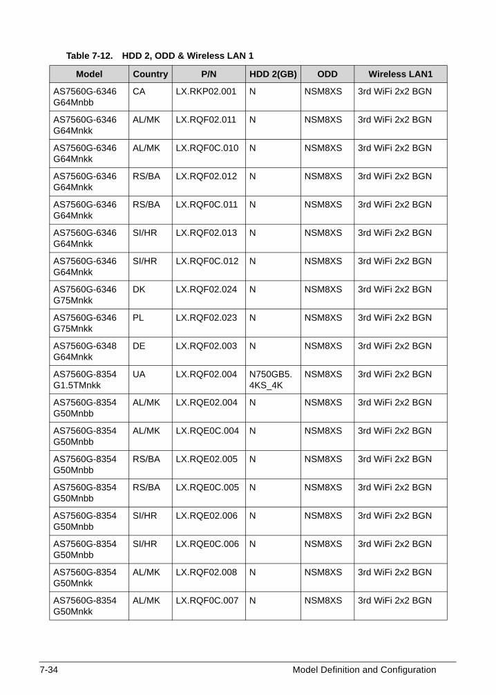
7-34 Model Definition and Configuration
AS7560G-6346G64Mnbb
CA LX.RKP02.001 N NSM8XS 3rd WiFi 2x2 BGN
AS7560G-6346G64Mnkk
AL/MK LX.RQF02.011 N NSM8XS 3rd WiFi 2x2 BGN
AS7560G-6346G64Mnkk
AL/MK LX.RQF0C.010 N NSM8XS 3rd WiFi 2x2 BGN
AS7560G-6346G64Mnkk
RS/BA LX.RQF02.012 N NSM8XS 3rd WiFi 2x2 BGN
AS7560G-6346G64Mnkk
RS/BA LX.RQF0C.011 N NSM8XS 3rd WiFi 2x2 BGN
AS7560G-6346G64Mnkk
SI/HR LX.RQF02.013 N NSM8XS 3rd WiFi 2x2 BGN
AS7560G-6346G64Mnkk
SI/HR LX.RQF0C.012 N NSM8XS 3rd WiFi 2x2 BGN
AS7560G-6346G75Mnkk
DK LX.RQF02.024 N NSM8XS 3rd WiFi 2x2 BGN
AS7560G-6346G75Mnkk
PL LX.RQF02.023 N NSM8XS 3rd WiFi 2x2 BGN
AS7560G-6348G64Mnkk
DE LX.RQF02.003 N NSM8XS 3rd WiFi 2x2 BGN
AS7560G-8354G1.5TMnkk
UA LX.RQF02.004 N750GB5.4KS_4K
NSM8XS 3rd WiFi 2x2 BGN
AS7560G-8354G50Mnbb
AL/MK LX.RQE02.004 N NSM8XS 3rd WiFi 2x2 BGN
AS7560G-8354G50Mnbb
AL/MK LX.RQE0C.004 N NSM8XS 3rd WiFi 2x2 BGN
AS7560G-8354G50Mnbb
RS/BA LX.RQE02.005 N NSM8XS 3rd WiFi 2x2 BGN
AS7560G-8354G50Mnbb
RS/BA LX.RQE0C.005 N NSM8XS 3rd WiFi 2x2 BGN
AS7560G-8354G50Mnbb
SI/HR LX.RQE02.006 N NSM8XS 3rd WiFi 2x2 BGN
AS7560G-8354G50Mnbb
SI/HR LX.RQE0C.006 N NSM8XS 3rd WiFi 2x2 BGN
AS7560G-8354G50Mnkk
AL/MK LX.RQF02.008 N NSM8XS 3rd WiFi 2x2 BGN
AS7560G-8354G50Mnkk
AL/MK LX.RQF0C.007 N NSM8XS 3rd WiFi 2x2 BGN
Table 7-12. HDD 2, ODD & Wireless LAN 1
Model Country P/N HDD 2(GB) ODD Wireless LAN1

Model Definition and Configuration 7-35
AS7560G-8354G50Mnkk
DE LX.RQF02.021 N NSM8XS 3rd WiFi 2x2 BGN
AS7560G-8354G50Mnkk
RS/BA LX.RQF02.009 N NSM8XS 3rd WiFi 2x2 BGN
AS7560G-8354G50Mnkk
RS/BA LX.RQF0C.008 N NSM8XS 3rd WiFi 2x2 BGN
AS7560G-8354G50Mnkk
SI/HR LX.RQF02.010 N NSM8XS 3rd WiFi 2x2 BGN
AS7560G-8354G50Mnkk
SI/HR LX.RQF0C.009 N NSM8XS 3rd WiFi 2x2 BGN
AS7560G-8358G1.5TMnkk
DK LX.RQF02.019 N750GB5.4KS_4K
NSM8XS 3rd WiFi 2x2 BGN
AS7560G-8358G1TMnkk
AL/MK LX.RQF0C.013 N500GB5.4KS
NSM8XS 3rd WiFi 2x2 BGN
AS7560G-8358G1TMnkk
DK LX.RQF02.025 N500GB5.4KS_4K
NSM8XS 3rd WiFi 2x2 BGN
AS7560G-8358G1TMnkk
RS/BA LX.RQF0C.014 N500GB5.4KS
NSM8XS 3rd WiFi 2x2 BGN
AS7560G-8358G1TMnkk
SI/HR LX.RQF0C.015 N500GB5.4KS
NSM8XS 3rd WiFi 2x2 BGN
AS7560G-8358G75Mnkk
AL/MK LX.RQF02.014 N NSM8XS 3rd WiFi 2x2 BGN
AS7560G-8358G75Mnkk
RS/BA LX.RQF02.015 N NSM8XS 3rd WiFi 2x2 BGN
AS7560G-8358G75Mnkk
SI/HR LX.RQF02.016 N NSM8XS 3rd WiFi 2x2 BGN
Table 7-13. Bluetooth & NB Chipset
Model Country P/N Bluetooth NB Chipset
AS7560G-4334G32Mnkk
IT LX.RQF02.017 N AMD A60M FCH
AS7560G-4334G50Mnbb
AL/MK LX.RKP02.004 BT 3.0 AMD A60M FCH
AS7560G-4334G50Mnbb
RS/BA LX.RKP02.002 BT 3.0 AMD A60M FCH
AS7560G-4334G50Mnbb
SI/HR LX.RKP02.003 BT 3.0 AMD A60M FCH
AS7560G-4334G50Mnbb
UA LX.RKP0C.001 N AMD A60M FCH
Table 7-12. HDD 2, ODD & Wireless LAN 1
Model Country P/N HDD 2(GB) ODD Wireless LAN1

7-36 Model Definition and Configuration
AS7560G-4334G50Mnkk
AL/MK LX.RKN02.004 BT 3.0 AMD A60M FCH
AS7560G-4334G50Mnkk
AL/MK LX.RKN0C.001 BT 2.1 AMD A60M FCH
AS7560G-4334G50Mnkk
AL/MK LX.RQF02.005 BT 3.0 AMD A60M FCH
AS7560G-4334G50Mnkk
AL/MK LX.RQF0C.004 BT 2.1 AMD A60M FCH
AS7560G-4334G50Mnkk
DE LX.RKN02.009 N AMD A60M FCH
AS7560G-4334G50Mnkk
RS/BA LX.RKN02.005 BT 3.0 AMD A60M FCH
AS7560G-4334G50Mnkk
RS/BA LX.RKN0C.002 BT 2.1 AMD A60M FCH
AS7560G-4334G50Mnkk
RS/BA LX.RQF02.006 BT 3.0 AMD A60M FCH
AS7560G-4334G50Mnkk
RS/BA LX.RQF0C.005 BT 2.1 AMD A60M FCH
AS7560G-4334G50Mnkk
SI/HR LX.RKN02.006 BT 3.0 AMD A60M FCH
AS7560G-4334G50Mnkk
SI/HR LX.RKN0C.003 BT 2.1 AMD A60M FCH
AS7560G-4334G50Mnkk
SI/HR LX.RQF02.007 BT 3.0 AMD A60M FCH
AS7560G-4334G50Mnkk
SI/HR LX.RQF0C.006 BT 2.1 AMD A60M FCH
AS7560G-4334G75Mnkk
CH LX.RKN02.008 N AMD A60M FCH
AS7560G-4336G50Mnkk
DK LX.RKN02.010 N AMD A60M FCH
AS7560G-6344G32Mnkk
DE LX.RKN02.003 N AMD A60M FCH
AS7560G-6344G32Mnkk
DE LX.RQF02.002 N AMD A60M FCH
AS7560G-6344G50Mnbb
AL/MK LX.RQE02.001 BT 3.0 AMD A60M FCH
AS7560G-6344G50Mnbb
AL/MK LX.RQE0C.001 BT 2.1 AMD A60M FCH
AS7560G-6344G50Mnbb
RS/BA LX.RQE02.002 BT 3.0 AMD A60M FCH
Table 7-13. Bluetooth & NB Chipset (Continued)
Model Country P/N Bluetooth NB Chipset

Model Definition and Configuration 7-37
AS7560G-6344G50Mnbb
RS/BA LX.RQE0C.002 BT 2.1 AMD A60M FCH
AS7560G-6344G50Mnbb
SI/HR LX.RQE02.003 BT 3.0 AMD A60M FCH
AS7560G-6344G50Mnbb
SI/HR LX.RQE0C.003 BT 2.1 AMD A60M FCH
AS7560G-6344G50Mnkk
AL/MK LX.RQF0C.001 BT 2.1 AMD A60M FCH
AS7560G-6344G50Mnkk
PL LX.RQF02.022 N AMD A60M FCH
AS7560G-6344G50Mnkk
RS/BA LX.RQF0C.002 BT 2.1 AMD A60M FCH
AS7560G-6344G50Mnkk
SI/HR LX.RQF0C.003 BT 2.1 AMD A60M FCH
AS7560G-6344G64Mnbb
PL LX.RQE02.007 N AMD A60M FCH
AS7560G-6344G64Mnkk
IT LX.RKN02.001 N AMD A60M FCH
AS7560G-6344G64Mnkk
PL LX.RQF02.020 N AMD A60M FCH
AS7560G-6344G75Mnbb
UA LX.RQE01.001 BT 3.0 AMD A60M FCH
AS7560G-6344G75Mnkk
DK LX.RKN02.007 N AMD A60M FCH
AS7560G-6344G75Mnkk
DK LX.RQF02.018 N AMD A60M FCH
AS7560G-6344G75Mnkk
IT LX.RQF02.001 N AMD A60M FCH
AS7560G-6346G64Mnbb
CA LX.RKP02.001 N AMD A60M FCH
AS7560G-6346G64Mnkk
AL/MK LX.RQF02.011 BT 3.0 AMD A60M FCH
AS7560G-6346G64Mnkk
AL/MK LX.RQF0C.010 BT 2.1 AMD A60M FCH
AS7560G-6346G64Mnkk
RS/BA LX.RQF02.012 BT 3.0 AMD A60M FCH
AS7560G-6346G64Mnkk
RS/BA LX.RQF0C.011 BT 2.1 AMD A60M FCH
AS7560G-6346G64Mnkk
SI/HR LX.RQF02.013 BT 3.0 AMD A60M FCH
Table 7-13. Bluetooth & NB Chipset (Continued)
Model Country P/N Bluetooth NB Chipset

7-38 Model Definition and Configuration
AS7560G-6346G64Mnkk
SI/HR LX.RQF0C.012 BT 2.1 AMD A60M FCH
AS7560G-6346G75Mnkk
DK LX.RQF02.024 N AMD A60M FCH
AS7560G-6346G75Mnkk
PL LX.RQF02.023 N AMD A60M FCH
AS7560G-6348G64Mnkk
DE LX.RQF02.003 N AMD A60M FCH
AS7560G-8354G1.5TMnkk
UA LX.RQF02.004 BT 3.0 AMD A60M FCH
AS7560G-8354G50Mnbb
AL/MK LX.RQE02.004 BT 3.0 AMD A60M FCH
AS7560G-8354G50Mnbb
AL/MK LX.RQE0C.004 BT 2.1 AMD A60M FCH
AS7560G-8354G50Mnbb
RS/BA LX.RQE02.005 BT 3.0 AMD A60M FCH
AS7560G-8354G50Mnbb
RS/BA LX.RQE0C.005 BT 2.1 AMD A60M FCH
AS7560G-8354G50Mnbb
SI/HR LX.RQE02.006 BT 3.0 AMD A60M FCH
AS7560G-8354G50Mnbb
SI/HR LX.RQE0C.006 BT 2.1 AMD A60M FCH
AS7560G-8354G50Mnkk
AL/MK LX.RQF02.008 BT 3.0 AMD A60M FCH
AS7560G-8354G50Mnkk
AL/MK LX.RQF0C.007 BT 2.1 AMD A60M FCH
AS7560G-8354G50Mnkk
DE LX.RQF02.021 N AMD A60M FCH
AS7560G-8354G50Mnkk
RS/BA LX.RQF02.009 BT 3.0 AMD A60M FCH
AS7560G-8354G50Mnkk
RS/BA LX.RQF0C.008 BT 2.1 AMD A60M FCH
AS7560G-8354G50Mnkk
SI/HR LX.RQF02.010 BT 3.0 AMD A60M FCH
AS7560G-8354G50Mnkk
SI/HR LX.RQF0C.009 BT 2.1 AMD A60M FCH
AS7560G-8358G1.5TMnkk
DK LX.RQF02.019 BT 3.0 AMD A60M FCH
AS7560G-8358G1TMnkk
AL/MK LX.RQF0C.013 BT 2.1 AMD A60M FCH
Table 7-13. Bluetooth & NB Chipset (Continued)
Model Country P/N Bluetooth NB Chipset

Model Definition and Configuration 7-39
AS7560G-8358G1TMnkk
DK LX.RQF02.025 N AMD A60M FCH
AS7560G-8358G1TMnkk
RS/BA LX.RQF0C.014 BT 2.1 AMD A60M FCH
AS7560G-8358G1TMnkk
SI/HR LX.RQF0C.015 BT 2.1 AMD A60M FCH
AS7560G-8358G75Mnkk
AL/MK LX.RQF02.014 BT 3.0 AMD A60M FCH
AS7560G-8358G75Mnkk
RS/BA LX.RQF02.015 BT 3.0 AMD A60M FCH
AS7560G-8358G75Mnkk
SI/HR LX.RQF02.016 BT 3.0 AMD A60M FCH
Table 7-14. Battery & Adapter
Model Country P/N Battery Adapter
AS7560G-4334G32Mnkk
IT LX.RQF02.017 6CELL2.2 90W
AS7560G-4334G50Mnbb
AL/MK LX.RKP02.004 6CELL2.2 90W
AS7560G-4334G50Mnbb
RS/BA LX.RKP02.002 6CELL2.2 90W
AS7560G-4334G50Mnbb
SI/HR LX.RKP02.003 6CELL2.2 90W
AS7560G-4334G50Mnbb
UA LX.RKP0C.001 6CELL2.2 90W
AS7560G-4334G50Mnkk
AL/MK LX.RKN02.004 6CELL2.2 90W
AS7560G-4334G50Mnkk
AL/MK LX.RKN0C.001 6CELL2.2 90W
AS7560G-4334G50Mnkk
AL/MK LX.RQF02.005 6CELL2.2 90W
AS7560G-4334G50Mnkk
AL/MK LX.RQF0C.004 6CELL2.2 90W
AS7560G-4334G50Mnkk
DE LX.RKN02.009 6CELL2.2 90W
AS7560G-4334G50Mnkk
RS/BA LX.RKN02.005 6CELL2.2 90W
AS7560G-4334G50Mnkk
RS/BA LX.RKN0C.002 6CELL2.2 90W
Table 7-13. Bluetooth & NB Chipset (Continued)
Model Country P/N Bluetooth NB Chipset

7-40 Model Definition and Configuration
AS7560G-4334G50Mnkk
RS/BA LX.RQF02.006 6CELL2.2 90W
AS7560G-4334G50Mnkk
RS/BA LX.RQF0C.005 6CELL2.2 90W
AS7560G-4334G50Mnkk
SI/HR LX.RKN02.006 6CELL2.2 90W
AS7560G-4334G50Mnkk
SI/HR LX.RKN0C.003 6CELL2.2 90W
AS7560G-4334G50Mnkk
SI/HR LX.RQF02.007 6CELL2.2 90W
AS7560G-4334G50Mnkk
SI/HR LX.RQF0C.006 6CELL2.2 90W
AS7560G-4334G75Mnkk
CH LX.RKN02.008 6CELL2.2 90W
AS7560G-4336G50Mnkk
DK LX.RKN02.010 6CELL2.2 90W
AS7560G-6344G32Mnkk
DE LX.RKN02.003 6CELL2.2 90W
AS7560G-6344G32Mnkk
DE LX.RQF02.002 6CELL2.2 90W
AS7560G-6344G50Mnbb
AL/MK LX.RQE02.001 6CELL2.2 90W
AS7560G-6344G50Mnbb
AL/MK LX.RQE0C.001 6CELL2.2 90W
AS7560G-6344G50Mnbb
RS/BA LX.RQE02.002 6CELL2.2 90W
AS7560G-6344G50Mnbb
RS/BA LX.RQE0C.002 6CELL2.2 90W
AS7560G-6344G50Mnbb
SI/HR LX.RQE02.003 6CELL2.2 90W
AS7560G-6344G50Mnbb
SI/HR LX.RQE0C.003 6CELL2.2 90W
AS7560G-6344G50Mnkk
AL/MK LX.RQF0C.001 6CELL2.2 90W
AS7560G-6344G50Mnkk
PL LX.RQF02.022 6CELL2.2 90W
AS7560G-6344G50Mnkk
RS/BA LX.RQF0C.002 6CELL2.2 90W
AS7560G-6344G50Mnkk
SI/HR LX.RQF0C.003 6CELL2.2 90W
Table 7-14. Battery & Adapter (Continued)
Model Country P/N Battery Adapter

Model Definition and Configuration 7-41
AS7560G-6344G64Mnbb
PL LX.RQE02.007 6CELL2.2 90W
AS7560G-6344G64Mnkk
IT LX.RKN02.001 6CELL2.2 90W
AS7560G-6344G64Mnkk
PL LX.RQF02.020 6CELL2.2 90W
AS7560G-6344G75Mnbb
UA LX.RQE01.001 6CELL2.2 90W
AS7560G-6344G75Mnkk
DK LX.RKN02.007 6CELL2.2 90W
AS7560G-6344G75Mnkk
DK LX.RQF02.018 6CELL2.2 90W
AS7560G-6344G75Mnkk
IT LX.RQF02.001 6CELL2.2 90W
AS7560G-6346G64Mnbb
CA LX.RKP02.001 6CELL2.2 90W
AS7560G-6346G64Mnkk
AL/MK LX.RQF02.011 6CELL2.2 90W
AS7560G-6346G64Mnkk
AL/MK LX.RQF0C.010 6CELL2.2 90W
AS7560G-6346G64Mnkk
RS/BA LX.RQF02.012 6CELL2.2 90W
AS7560G-6346G64Mnkk
RS/BA LX.RQF0C.011 6CELL2.2 90W
AS7560G-6346G64Mnkk
SI/HR LX.RQF02.013 6CELL2.2 90W
AS7560G-6346G64Mnkk
SI/HR LX.RQF0C.012 6CELL2.2 90W
AS7560G-6346G75Mnkk
DK LX.RQF02.024 6CELL2.2 90W
AS7560G-6346G75Mnkk
PL LX.RQF02.023 6CELL2.2 90W
AS7560G-6348G64Mnkk
DE LX.RQF02.003 6CELL2.2 90W
AS7560G-8354G1.5TMnkk
UA LX.RQF02.004 6CELL2.2 90W
AS7560G-8354G50Mnbb
AL/MK LX.RQE02.004 6CELL2.2 90W
AS7560G-8354G50Mnbb
AL/MK LX.RQE0C.004 6CELL2.2 90W
Table 7-14. Battery & Adapter (Continued)
Model Country P/N Battery Adapter

7-42 Model Definition and Configuration
AS7560G-8354G50Mnbb
RS/BA LX.RQE02.005 6CELL2.2 90W
AS7560G-8354G50Mnbb
RS/BA LX.RQE0C.005 6CELL2.2 90W
AS7560G-8354G50Mnbb
SI/HR LX.RQE02.006 6CELL2.2 90W
AS7560G-8354G50Mnbb
SI/HR LX.RQE0C.006 6CELL2.2 90W
AS7560G-8354G50Mnkk
AL/MK LX.RQF02.008 6CELL2.2 90W
AS7560G-8354G50Mnkk
AL/MK LX.RQF0C.007 6CELL2.2 90W
AS7560G-8354G50Mnkk
DE LX.RQF02.021 6CELL2.2 90W
AS7560G-8354G50Mnkk
RS/BA LX.RQF02.009 6CELL2.2 90W
AS7560G-8354G50Mnkk
RS/BA LX.RQF0C.008 6CELL2.2 90W
AS7560G-8354G50Mnkk
SI/HR LX.RQF02.010 6CELL2.2 90W
AS7560G-8354G50Mnkk
SI/HR LX.RQF0C.009 6CELL2.2 90W
AS7560G-8358G1.5TMnkk
DK LX.RQF02.019 6CELL2.2 90W
AS7560G-8358G1TMnkk
AL/MK LX.RQF0C.013 6CELL2.2 90W
AS7560G-8358G1TMnkk
DK LX.RQF02.025 6CELL2.2 90W
AS7560G-8358G1TMnkk
RS/BA LX.RQF0C.014 6CELL2.2 90W
AS7560G-8358G1TMnkk
SI/HR LX.RQF0C.015 6CELL2.2 90W
AS7560G-8358G75Mnkk
AL/MK LX.RQF02.014 6CELL2.2 90W
AS7560G-8358G75Mnkk
RS/BA LX.RQF02.015 6CELL2.2 90W
AS7560G-8358G75Mnkk
SI/HR LX.RQF02.016 6CELL2.2 90W
Table 7-14. Battery & Adapter (Continued)
Model Country P/N Battery Adapter

CHAPTER 8
Test Compatible Components

8-2
Microsoft® Windows® 7 Environment Test. . . . . . . . . . . . . . . . 8-4Aspire 7560/7560G . . . . . . . . . . . . . . . . . . . . . . . . . . . . . . . . . 8-4

Test Compatible Components 8-3
Test Compatible Components
This computer’s compatibility is tested and verified by Acer’s internal testing department. All of
its system functions are tested under Windows® 7 environment.
Refer to the following lists for components, adapter cards, and peripherals which have passed these tests. Regarding configuration, combination and test procedures, please refer to the Acer Aspire 7560/7560G. Compatibility Test Report released by the Acer Mobile System Testing Department.

8-4 Test Compatible Components
Microsoft® Windows® 7 Environment Test 0
Aspire 7560/7560G 0
Table 8-1. Aspire 7560/7560G
Vendor Type Description P/N
2nd HDD
60001922 TOSHIBA DIGI
N250GB5.4KS HDD TOSHIBA 2.5" 5400rpm 250GB MK2565GSX, Capricorn BS, 320G/P SATA 8MB LF F/W:GJ002J
KH.25004.005
60001922 TOSHIBA DIGI
N320GB5.4KS HDD TOSHIBA 2.5" 5400rpm 320GB Capricorn BS ,MK3265GSX SATA 8MB LF F/W:GJ002J
KH.32004.004
60001922 TOSHIBA DIGI
N320GB5.4KS_4K HDD TOSHIBA 2.5" 5400rpm 320GB MK3259GSXP, Capricorn 3BS, 375G/P, 4K drive SATA 8MB LF+HF F/W:GN003J 4K
KH.32004.005
60001922 TOSHIBA DIGI
N500GB5.4KS HDD TOSHIBA 2.5" 5400rpm 500GB MK5065GSX,Capricorn BS, 320G/P SATA 8MB LF F/W:GJ002J
KH.50004.002
60001922 TOSHIBA DIGI
N500GB5.4KS_4K HDD TOSHIBA 2.5" 5400rpm 500GB MK5059GSXP, Capricron 3BS, 375G/P SATA 8MB LF+HF F/W:GN003J 4K
KH.50004.003
60001922 TOSHIBA DIGI
N640GB5.4KS HDD TOSHIBA 2.5" 5400rpm 640GB MK6465GSX,Capricorn BS,320G/P SATA 8MB LF F/W:GJ002J
KH.64004.001
60001922 TOSHIBA DIGI
N640GB5.4KS_4K HDD TOSHIBA 2.5" 5400rpm 640GB MK6459GSXP, Capricron 3BS, 375G/P SATA 8MB LF+HF F/W:GN003J 4K
KH.64004.003
60001922 TOSHIBA DIGI
N750GB5.4KS_4K HDD TOSHIBA 2.5" 5400rpm 750GB MK7559GSXP, 375G/P, Capricorn BS, 4K drive SATA 8MB LF+HF F/W:GN003J
KH.75004.001
60001994 WD N160GB5.4KS_4K HDD WD 2.5" 5400rpm 160GB WD1600BPVT-22ZEST0, 4K , ML320S-AF SATA 8MB LF F/W:01.01A01 4K drive
KH.16008.028

Test Compatible Components 8-5
60001994 WD N250GB5.4KS_4K HDD WD 2.5" 5400rpm 250GB WD2500BPVT-22ZEST0,ML320S-AF, 4K drive SATA 8MB LF F/W:01.01A01 4K drive
KH.25008.029
60001994 WD N320GB5.4KS_4K HDD WD 2.5" 5400rpm 320GB WD3200BPVT-22ZEST0, ML320S, 4K drive SATA 8MB LF F/W: 01.01A01
KH.32008.022
60001994 WD N500GB5.4KS_4K HDD WD 2.5" 5400rpm 500GB WD5000BPVT-22HXZT1,ML375_AF, 4K drive SATA 8MB LF+HF F/W:01.01A01
KH.50008.021
60001994 WD N640GB5.4KS_4K HDD WD 2.5" 5400rpm 640GB WD6400BPVT-22HXZT1, ML375M SATA 8MB LF F/W: 01.01A01
KH.64008.005
60001994 WD N750GB5.4KS_4K HDD WD 2.5" 5400rpm 750GB WD7500BPVT-22HXZT1, ML375M, 4K drive SATA 8MB LF F/W:01.01A01
KH.75008.009
60002005 HGST SG
N160GB5.4KS HDD HGST 2.5" 5400rpm 160GB HTS545016B9A300 Panther B SATA LF F/W:C60F Disk imbalance criteria = 0.014g-cm
KH.16007.026
60002005 HGST SG
N250GB5.4KS HDD HGST 2.5" 5400rpm 250GB HTS545025B9A300 Panther B SATA LF F/W:C60F Disk imbalance criteria = 0.014g-cm
KH.25007.016
60002005 HGST SG
N320GB5.4KS HDD HGST 2.5" 5400rpm 320GB HTS545032B9A300 Panther B SATA LF F/W:C60F Disk imbalance criteria = 0.014g-cm
KH.32007.008
60002005 HGST SG
N320GB5.4KS HDD HGST 2.5" 5400rpm 320GB HTS543232A7A384, Eagle B7, 320G/P SATA LF+HF F/W:A60W
KH.32007.013
60002005 HGST SG
N500GB5.4KS HDD HGST 2.5" 5400rpm 500GB HTS545050B9A300 Panther B SATA LF F/W:C60F Disk imbalance criteria = 0.014g-cm
KH.50007.010
60002005 HGST SG
N640GB5.4KS_4K HDD HGST 2.5" 5400rpm 640GB HTS547564A9E384,Jet B, 375G/P SATA 8MB LF+HF F/W:DA3872
KH.64007.003
60002005 HGST SG
N750GB5.4KS HDD HGST 2.5" 5400rpm 750GB Dummy P.N SATA 8MB LF+HF F/W: 0000
KH.75007.005
Table 8-1. Aspire 7560/7560G (Continued)
Vendor Type Description P/N

8-6 Test Compatible Components
60002005 HGST SG
N750GB5.4KS_4K HDD HGST 2.5" 5400rpm 750GB HTS547575A9E384, Jet B, 375G/P SATA 8MB LF F/W:DA3872
KH.75007.004
60002036 SEAGATE
N250GB5.4KS HDD SEAGATE 2.5" 5400rpm 250GB ST9250315AS, 9HH132-189, Wyatt with new pcb SATA 8MB LF F/W:0001SDM1
KH.25001.019
60002036 SEAGATE
N320GB5.4KS HDD SEAGATE 2.5" 5400rpm 320GB ST9320310AS,9RN132-188, Cameron 320G/P SATA 8MB LF F/W:0001SDM1
KH.32001.019
60002036 SEAGATE
N500GB5.4KS HDD SEAGATE 2.5" 5400rpm 500GB ST9500325AS,9HH134-189, Wyatt with new pcb SATA 8MB LF F/W:0001SDM1
KH.50001.017
60002036 SEAGATE
N640GB5.4KS HDD SEAGATE 2.5" 5400rpm 640GB ST9640320AS,9RN134-189, Cameron, 320G/P SATA 8MB LF F/W:0001SDM1
KH.64001.004
60002036 SEAGATE
N750GB5.4KS_4K HDD SEAGATE 2.5" 5400rpm 750GB ST9750423AS,9ZW14G-188, Desaru5, 375G/P. SATA 8MB LF+HF F/W:0001SDM1
KH.75001.011
Adapter
10001023 LITE-ON
120W-DE Adapter LITE-ON 120W-DE 19V 1.7x5.5x11 Green PA-1121-04AC, LV5+OBL LED LF
AP.12003.003
10001023 LITE-ON
65W Adapter LITE-ON 65W 19V 1.7x5.5x11 Yellow PA-1650-22AC LV5 LED LF
AP.06503.024
10001023 LITE-ON
65W Adapter LITE-ON 65W 19V 1.7x5.5x11 Yellow PA-1650-69AW, LV5, Low profile LED LF
AP.06503.029
10001023 LITE-ON
90W Adapter LITE-ON 90W 19V 1.7x5.5x11 Blue PA-1900-34AR, LV5 LED LF
AP.09003.021
10001023 LITE-ON
90W Adapter LITE-ON 90W 19V 1.7x5.5x11 Blue PA-1900-32AW, LV5, Low profile LF
AP.09003.024
Table 8-1. Aspire 7560/7560G (Continued)
Vendor Type Description P/N

Test Compatible Components 8-7
10001045 DELTA-MACAO
90W Adapter DELTA 90W 19V 1.7x5.5x11 Blue ADP-90MD BBA, low profile, LV5 LF
AP.09001.032
10001081 DELTA
120W-DE Adapter DELTA 120W-DE 19V 1.7x5.5x11 Green ADP-120ZB BBGB, LV5+OBL LED LF
AP.12001.009
10001081 DELTA
65W Adapter DELTA 65W 19V 1.7x5.5x11 Yellow ADP-65JH DB A, LV5 LED LF
AP.06501.026
10001081 DELTA
65W Adapter DELTA 65W 19V 1.7x5.5x11 Yellow ADP-65VH BA, LV5, Low profile LED LF
AP.06501.033
10001081 DELTA
90W Adapter DELTA 90W 19V 1.7x5.5x11 Blue ADP-90CD DBH, LV5 LED LF
AP.09001.031
60002015 HIPRO
65W Adapter HIPRO 65W 19V 1.7x5.5x11 Yellow HP-A0652R3B 1LF, LV5 LED LF
AP.0650A.012
60002015 HIPRO
90W Adapter HIPRO 90W 19V 1.7x5.5x11 Blue HP-A0904A3 B1LF, LV5 LED LF
AP.0900A.005
60016453 CHICONY POWER
65W Adapter Chicony Power 65W 19V 1.7x5.5x11 Yellow CPA09-A065N1, LV5, low profile LF
AP.0650A.017
60016453 CHICONY POWER
90W Adapter Chicony Power 90W 19V 1.7x5.5x11 Blue A10-090P3A / A090A029L, LV5 low profile LF
AP.0900H.001
Audio Codec
10004786 REALTEK
ALC271X_VB3 Realtek ALC271X_VB3 LZ.21000.085
Battery
10001063 SONY
6CELL2.2 Battery SONY AS10D Li-Ion 3S2P SONY 6 cell 4400mAh Main COMMON ID:AS10D41
BT.00604.049
60001535 PANASONIC
6CELL2.2 Battery PANASONIC AS10D Li-Ion 3S2P PANASONIC 6 cell 4400mAh Main COMMON ID:AS10D51
BT.00605.062
60001921 SANYO
6CELL2.2 Battery SANYO AS10D Li-Ion 3S2P SANYO 6 cell 4400mAh Main COMMON ID:AS10D31
BT.00603.111
Table 8-1. Aspire 7560/7560G (Continued)
Vendor Type Description P/N

8-8 Test Compatible Components
60001921 SANYO
6CELL2.2 Battery SANYO AS10D Li-Ion 3S2P SANYO 6 cell 4400mAh Main COMMON new IC BQ8055
BT.00603.124
60001921 SANYO
9CELL3.0 Battery SANYO AS10G Li-Ion 3S3P SANYO 9 cell 9000mAh Main COMMON ID:AS10G3E
BT.00903.013
60002162 SIMPLO
6CELL2.2 Battery SIMPLO AS10D Li-Ion 3S2P PANASONIC 6 cell 4400mAh Main COMMON ID:AS10D71
BT.00607.125
60002162 SIMPLO
6CELL2.2 Battery SIMPLO AS10D Li-Ion 3S2P LGC 6 cell 4400mAh Main COMMON ID:AS10D73
BT.00607.126
60002162 SIMPLO
6CELL2.2 Battery SIMPLO AS10D Li-Ion 3S2P SAMSUNG 6 cell 4400mAh Main COMMON ID:AS10D
BT.00607.127
60013145 SAMSUNG SDI
6CELL2.2 Battery SAMSUNG AS10D Li-Ion 3S2P SAMSUNG 6 cell 4400mAh Main COMMON ID:AS10D61
BT.00606.008
Bluetooth
10001018 HON HAI
BT 2.1 Foxconn Bluetooth ATH BU_12 BH.21100.012
10001018 HON HAI
BT 3.0 Foxconn Bluetooth BRM 2046 BT3.0 (T60H928.33) f/w:861
BH.21100.008
10001018 HON HAI
BT 3.0 Foxconn Bluetooth ATH AR3011 (BT3.0)
BH.21100.009
10001018 HON HAI
BT 3.0 Foxconn Bluetooth BRM 2070 (T77H114.01) BT 3.0
BH.21100.010
10001018 HON HAI
BT 3.0 Foxconn Bluetooth ATH BU12 BH.21100.011
23707801 FOXCONN TW
BT 2.1 Foxconn Bluetooth BRM 2070 (T77H114.01)
BH.21100.007
Camera
10001023 LITE-ON
1.3M Liteon 1.3M LT9665AL (09P2SF119)
AM.21400.069
10001023 LITE-ON
1.3M Liteon 1.3M LT6AASP( 09P2BF127)
AM.21400.070
10001023 LITE-ON
1.3M Liteon 1.3M LT_6A1_SP AM.21400.081
10001023 LITE-ON
1.3M Liteon 1.3M LT_6A1_SP (9A) AM.21400.084
Table 8-1. Aspire 7560/7560G (Continued)
Vendor Type Description P/N

Test Compatible Components 8-9
10001023 LITE-ON
1.3M HD Liteon 1.3M LT_6A1(TSV)_SP AM.21400.089
10001023 LITE-ON
1.3M HD Liteon 1.3M HD LT_2659_AU AM.21400.095
10001023 LITE-ON
1.3M HD Liteon 1.3M LT_6A1(CSP)_SP AM.21400.092
10001023 LITE-ON
1.3M HD Liteon 1.3M HD LT_HN161_SP AM.21400.115
10001044 CHICONY
1.3M Chicony 1.3M CH9665SN (CNF9157)
AM.21400.067
10001044 CHICONY
1.3M Chicony 1.3M CH_6A1_SP AM.21400.082
10001044 CHICONY
1.3M Chicony 1.3M CH_6A1_SP (9A) AM.21400.085
10001044 CHICONY
1.3M HD Chicony 1.3M CH_6A1(TSV)_SP AM.21400.090
10001044 CHICONY
1.3M HD Chicony 1.3M CH_6A1(CSP)_SP AM.21400.093
10001044 CHICONY
1.3M HD Chicony 1.3M HD CH_6A1(CSP)_SN234
AM.21400.096
10001044 CHICONY
1.3M HD Chicony 1.3M HD CH_HY161_AU AM.21400.118
PLM00012 Suyin
1.3M Suyin 1.3M SY9665SN AM.21400.068
PLM00012 Suyin
1.3M Suyin 1.3M SY_6A1_SP AM.21400.083
PLM00012 Suyin
1.3M Suyin 1.3M SY_6A1_SP (9A) AM.21400.099
PLM00012 Suyin
1.3M HD Suyin 1.3M HD SY_6A1(TSV)_SP AM.21400.091
PLM00012 Suyin
1.3M HD Suyin 1.3M HD SY_6A1(CSP)_SP AM.21400.094
PLM00012 Suyin
1.3M HD Suyin 1.3M HD SY_2659_AU AM.21400.097
PLM00012 Suyin
1.3M HD Suyin 1.3M HD SY_HN161_AU AM.21400.112
Table 8-1. Aspire 7560/7560G (Continued)
Vendor Type Description P/N

8-10 Test Compatible Components
Card Reader
PLM00014 ODM
5 in 1-Build in 5 in 1-Build in MS, MS Pro, SD, SC, XD
CR.21500.013
CPU
60002168 AMD A43300M CPU AMD - A4-3300M 1.9G 2M 35W B0 HD6480M
KC.33002.A4M
60002168 AMD A63400M CPU AMD - A6-3400M 1.4G 4M 35W B0 HD6520M
KC.34002.A6M
60002168 AMD A83500M CPU AMD - A8-3500M 1.5G 4M 35W B0 HD6620M
KC.35002.A8M
60002168 AMD E23000M CPU AMD - E2-3000M 1.8G 1M 35W B0 HD6380M
KC.30002.E2M
HDD
10001067 INTEL
SSD25120 Flash Disk INTEL SSD NAND 120GB SSDSA2M120G2GC MM#910281 FW 2M03 9.5mm LF+HF
KF.1200N.001
60001922 TOSHIBA DIGI
N250GB5.4KS HDD TOSHIBA 2.5" 5400rpm 250GB MK2565GSX, Capricorn BS, 320G/P SATA 8MB LF F/W:GJ002J
KH.25004.005
60001922 TOSHIBA DIGI
N320GB5.4KS HDD TOSHIBA 2.5" 5400rpm 320GB Capricorn BS ,MK3265GSX SATA 8MB LF F/W:GJ002J
KH.32004.004
60001922 TOSHIBA DIGI
N320GB5.4KS_4K HDD TOSHIBA 2.5" 5400rpm 320GB MK3259GSXP, Capricorn 3BS, 375G/P, 4K drive SATA 8MB LF+HF F/W:GN003J 4K
KH.32004.005
60001922 TOSHIBA DIGI
N500GB5.4KS HDD TOSHIBA 2.5" 5400rpm 500GB MK5065GSX,Capricorn BS, 320G/P SATA 8MB LF F/W:GJ002J
KH.50004.002
60001922 TOSHIBA DIGI
N500GB5.4KS_4K HDD TOSHIBA 2.5" 5400rpm 500GB MK5059GSXP, Capricron 3BS, 375G/P SATA 8MB LF+HF F/W:GN003J 4K
KH.50004.003
60001922 TOSHIBA DIGI
N640GB5.4KS HDD TOSHIBA 2.5" 5400rpm 640GB MK6465GSX,Capricorn BS,320G/P SATA 8MB LF F/W:GJ002J
KH.64004.001
Table 8-1. Aspire 7560/7560G (Continued)
Vendor Type Description P/N
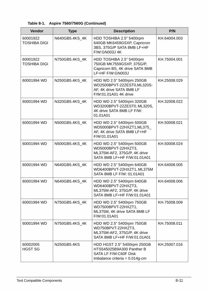
Test Compatible Components 8-11
60001922 TOSHIBA DIGI
N640GB5.4KS_4K HDD TOSHIBA 2.5" 5400rpm 640GB MK6459GSXP, Capricron 3BS, 375G/P SATA 8MB LF+HF F/W:GN003J 4K
KH.64004.003
60001922 TOSHIBA DIGI
N750GB5.4KS_4K HDD TOSHIBA 2.5" 5400rpm 750GB MK7559GSXP, 375G/P, Capricorn BS, 4K drive SATA 8MB LF+HF F/W:GN003J
KH.75004.001
60001994 WD N250GB5.4KS_4K HDD WD 2.5" 5400rpm 250GB WD2500BPVT-22ZEST0,ML320S-AF, 4K drive SATA 8MB LF F/W:01.01A01 4K drive
KH.25008.029
60001994 WD N320GB5.4KS_4K HDD WD 2.5" 5400rpm 320GB WD3200BPVT-22ZEST0, ML320S, 4K drive SATA 8MB LF F/W: 01.01A01
KH.32008.022
60001994 WD N500GB5.4KS_4K HDD WD 2.5" 5400rpm 500GB WD5000BPVT-22HXZT1,ML375_AF, 4K drive SATA 8MB LF+HF F/W:01.01A01
KH.50008.021
60001994 WD N500GB5.4KS_4K HDD WD 2.5" 5400rpm 500GB WD5000BPVT-22HXZT3, ML375M-AF2, 375G/P, 4K drive SATA 8MB LF+HF F/W:01.01A01
KH.50008.024
60001994 WD N640GB5.4KS_4K HDD WD 2.5" 5400rpm 640GB WD6400BPVT-22HXZT1, ML375M SATA 8MB LF F/W: 01.01A01
KH.64008.005
60001994 WD N640GB5.4KS_4K HDD WD 2.5" 5400rpm 640GB WD6400BPVT-22HXZT3, ML375M-AF2, 375G/P, 4K drive SATA 8MB LF+HF F/W:01.01A01
KH.64008.006
60001994 WD N750GB5.4KS_4K HDD WD 2.5" 5400rpm 750GB WD7500BPVT-22HXZT1, ML375M, 4K drive SATA 8MB LF F/W:01.01A01
KH.75008.009
60001994 WD N750GB5.4KS_4K HDD WD 2.5" 5400rpm 750GB WD750BPVT-22HXZT3, ML375M-AF2, 375G/P, 4K drive SATA 8MB LF+HF F/W:01.01A01
KH.75008.011
60002005 HGST SG
N250GB5.4KS HDD HGST 2.5" 5400rpm 250GB HTS545025B9A300 Panther B SATA LF F/W:C60F Disk imbalance criteria = 0.014g-cm
KH.25007.016
Table 8-1. Aspire 7560/7560G (Continued)
Vendor Type Description P/N

8-12 Test Compatible Components
60002005 HGST SG
N320GB5.4KS HDD HGST 2.5" 5400rpm 320GB HTS545032B9A300 Panther B SATA LF F/W:C60F Disk imbalance criteria = 0.014g-cm
KH.32007.008
60002005 HGST SG
N320GB5.4KS HDD HGST 2.5" 5400rpm 320GB HTS543232A7A384, Eagle B7, 320G/P SATA LF+HF F/W:A60W
KH.32007.013
60002005 HGST SG
N500GB5.4KS HDD HGST 2.5" 5400rpm 500GB HTS545050B9A300 Panther B SATA LF F/W:C60F Disk imbalance criteria = 0.014g-cm
KH.50007.010
60002005 HGST SG
N640GB5.4KS_4K HDD HGST 2.5" 5400rpm 640GB HTS547564A9E384,Jet B, 375G/P SATA 8MB LF+HF F/W:DA3872
KH.64007.003
60002005 HGST SG
N750GB5.4KS HDD HGST 2.5" 5400rpm 750GB Dummy P.N SATA 8MB LF+HF F/W: 0000
KH.75007.005
60002005 HGST SG
N750GB5.4KS_4K HDD HGST 2.5" 5400rpm 750GB HTS547575A9E384, Jet B, 375G/P SATA 8MB LF F/W:DA3872
KH.75007.004
60002036 SEAGATE
N250GB5.4KS HDD SEAGATE 2.5" 5400rpm 250GB ST9250315AS, 9HH132-189, Wyatt with new pcb SATA 8MB LF F/W:0001SDM1
KH.25001.019
60002036 SEAGATE
N320GB5.4KS HDD SEAGATE 2.5" 5400rpm 320GB ST9320310AS,9RN132-188, Cameron 320G/P SATA 8MB LF F/W:0001SDM1
KH.32001.019
60002036 SEAGATE
N500GB5.4KS HDD SEAGATE 2.5" 5400rpm 500GB ST9500325AS,9HH134-189, Wyatt with new pcb SATA 8MB LF F/W:0001SDM1
KH.50001.017
60002036 SEAGATE
N640GB5.4KS HDD SEAGATE 2.5" 5400rpm 640GB ST9640320AS,9RN134-189, Cameron, 320G/P SATA 8MB LF F/W:0001SDM1
KH.64001.004
60002036 SEAGATE
N750GB5.4KS_4K HDD SEAGATE 2.5" 5400rpm 750GB ST9750423AS,9ZW14G-188, Desaru5, 375G/P. SATA 8MB LF+HF F/W:0001SDM1
KH.75001.011
Table 8-1. Aspire 7560/7560G (Continued)
Vendor Type Description P/N

Test Compatible Components 8-13
Keyboard
60004864 DARFON
AC7T_A10B Keyboard ACER AC7T_A10B AC7T Internal 17 Standard Black NONE Y2010 Acer Texture
KB.I170A.143
LAN
10017383 Atheros
AR8151L Atheros AR8151L NI.22400.048
LCD
10001022 CMI NLED17.3WXGA+G LED LCD CMO 17.3'' WXGA+ Glare N173FGE-L21 LF 220nit 8ms 650:1
LK.1730D.002
10001038 CMO NLED17.3WXGA+G LED LCD CMO 17.3" WXGA+ Glare N173O6-L02 LF 220nit 8ms 600:1
LK.1730D.001
60002215 SAMSUNG
NLED17.3WXGA+G LED LCD SAMSUNG 17.3'' WXGA+ Glare LTN173KT01-A01 LF 220nit 8ms 600:1
LK.17306.001
60003089 LG NLED17.3WXGA+G LED LCD LPL 17.3" WXGA+ Glare LP173WD1-TLA3 LF 220nit 8ms 600:1
LK.17308.002
60003089 LG NLED17.3WXGA+G LED LCD LPL 17.3'' WXGA+ Glare LP173WD1-TLN1 LF 220nit 8ms 600:1
LK.17308.003
60003316 AUO NLED17.3WXGA+G LED LCD AUO 17.3'' WXGA+ Glare B173RW01-V3 LF 220nit 8ms 500:1
LK.17305.002
MEM
60001993 NANYA
SO1GBIII13 Memory NANYA SO-DIMM DDRIII 1333 1GB NT1GC64BH4B0PS-CG LF 128*16 0.055um
KN.1GB03.034
60001993 NANYA
SO2GBIII13 Memory NANYA SO-DIMM DDRIII 1333 2GB NT2GC64B88B0NS-CG LF 256*8 0.055um
KN.2GB03.021
60001993 NANYA
SO4GBIII13 Memory NANYA SO-DIMM DDRIII 1333 4GB NT4GC64B8HB0NS-CG LF 256*8 0.055um
KN.4GB03.005
60002000 UNIFOSA
SO1GBIII13 Memory UNIFOSA SO-DIMM DDRIII 1333 1GB GU672203EP0200 LF 128*8 0.065um
KN.1GB0H.017
Table 8-1. Aspire 7560/7560G (Continued)
Vendor Type Description P/N

8-14 Test Compatible Components
60002041 QIMONDA
SO1GBIII10 Memory NONE REG-ECC DDRIII 1066 1GB phantom p/n LF
KN.1GB00.003
60002041 QIMONDA
SO1GBIII10 Memory NONE SO-DIMM DDRIII 1066 1GB phantom p/n LF
KN.1GB00.005
60002045 HYNIX
SO2GBIII13 Memory HYNIX SO-DIMM DDRIII 1333 2GB HMT325S6BFR8C-H9 LF 256*8 46nm
KN.2GB0G.018
60002045 HYNIX
SO4GBIII13 Memory HYNIX SO-DIMM DDRIII 1333 4GB HMT351S6AFR8C-H9 LF 256*8 0.055um
KN.4GB0G.003
60002050 MICRON SG
SO2GBIII13 Memory MICRON SO-DIMM DDRIII 1333 2GB MT8JSF25664HZ-1G4D1 LF 256*8 0.055um
KN.2GB04.017
60002215 SAMSUNG
SO1GBIII13 Memory SAMSUNG SO-DIMM DDRIII 1333 1GB M471B2873FHS-CH9 LF 128*8 46nm
KN.1GB0B.035
60002215 SAMSUNG
SO2GBIII10 Memory NONE SO-DIMM DDRIII 1066 2GB dummy 1066 LF
KN.2GB00.001
60002215 SAMSUNG
SO2GBIII13 Memory SAMSUNG SO-DIMM DDRIII 1333 2GB M471B5673FH0-CH9 LF 128*8 46nm
KN.2GB0B.023
60002215 SAMSUNG
SO2GBIII13 Memory SAMSUNG SO-DIMM DDRIII 1333 2GB M471B5773CHS-CH9 LF 256*8 46nm
KN.2GB0B.026
60002215 SAMSUNG
SO2GBIII13 Memory SAMSUNG SO-DIMM DDRIII 1333 2GB M471B5773DH0-CH9 LF 256*8
KN.2GB0B.030
60002215 SAMSUNG
SO4GBIII10 Memory SAMSUNG SO-DIMM DDRIII 1066 4GB M471B5273BH1-CF8 LF 256*8 0.055um
KN.4GB0B.007
60002215 SAMSUNG
SO4GBIII13 Memory SAMSUNG SO-DIMM DDRIII 1333 4GB M471B5273CH0-CH9 LF 256*8 46nm
KN.4GB0B.010
60002215 SAMSUNG
SO4GBIII13 Memory SAMSUNG SO-DIMM DDRIII 1333 4GB M471B5273DH0-CH9 LF 256*8 35nm
KN.4GB0B.015
Table 8-1. Aspire 7560/7560G (Continued)
Vendor Type Description P/N

Test Compatible Components 8-15
60004668 ELPIDA
SO2GBIII13 Memory ELPIDA SO-DIMM DDRIII 1333 2GB EBJ21UE8BFU0-DJ-F LF 128*8 0.065um
KN.2GB09.009
60004668 ELPIDA
SO2GBIII13 Memory ELPIDA SO-DIMM DDRIII 1333 2GB EBJ20UF8BCS0-DJ-F LF 256*8 46nm
KN.2GB09.010
60004668 ELPIDA
SO4GBIII10 Memory NONE SO-DIMM DDRIII 1066 4GB dummy P/N LF
KN.4GB00.001
60004668 ELPIDA
SO4GBIII13 Memory ELPIDA SO-DIMM DDRIII 1333 4GB EBJ41UF8BAS0-DJ-F LF 256*8 0.055um
KN.4GB09.001
60024207 KINGSTON-FAR EAST
SO1GBIII13 Memory KINGSTON SO-DIMM DDRIII 1333 1GB ACR128X64D3S1333C9 LF 128*8 0.065um
KN.1GB07.004
60024207 KINGSTON-FAR EAST
SO2GBIII13 Memory KINGSTON SO-DIMM DDRIII 1333 2GB ACR256X64D3S1333C9 LF 128*8 0.065um
KN.2GB07.004
60024207 KINGSTON-FAR EAST
SO2GBIII13 Memory KINGSTON SO-DIMM DDRIII 1333 2GB ACR256X64D3S13C9G LF+HF
KN.2GB07.006
60024207 KINGSTON-FAR EAST
SO4GBIII13 Memory KINGSTON SO-DIMM DDRIII 1333 4GB ACR512X64D3S13C9G LF+HF
KN.4GB07.001
NB Chipset
60002168 AMD AMD A60M FCH AMD NB Chipset A60M KI.22600.059
60002168 AMD AMD A70M FCH AMD NB Chipset A70M KI.22600.060
ODD
10001063 SONY
NSM8XS ODD SONY Super-Multi DRIVE 12.7mm Tray DL 8X AD-7585H LF W/O bezel SATA (HF + Windows 7)
KU.0080E.027
10001070 PHILIPS
NBDCB4XS ODD PLDS BD COMBO 12.7mm Tray DL 4X DS-6E2SH LF W/O bezel SATA (HF + Win7 + 3D)
KO.0040F.006
10001070 PHILIPS
NSM8XS ODD PLDS Super-Multi DRIVE 12.7mm Tray DL 8X DS-8A5SH LF+HF W/O bezel SATA With TI + Rohm Solution (HF + Windows 7)
KU.0080F.014
60001535 PANASONIC
NBDCB4XS ODD PANASONIC BD COMBO 12.7mm Tray DL 4X UJ141AL LF W/O bezel SATA Windows 7
KO.00407.004
Table 8-1. Aspire 7560/7560G (Continued)
Vendor Type Description P/N

8-16 Test Compatible Components
60001535 PANASONIC
NBDCB4XS ODD PANASONIC BD COMBO 12.7mm Tray DL 4X UJ141AJ LF W/O bezel SATA Zero Power + BUS Encryption
KO.00407.006
60001535 PANASONIC
NBDRW4XS ODD PANASONIC BD RW 12.7mm Tray DL 4X UJ240A LF W/O bezel SATA (HF+Windows 7)
KU.00407.015
60001535 PANASONIC
NSM8XS ODD PANASONIC Super-Multi DRIVE 12.7mm Tray DL 8X UJ890A LF W/O bezel SATA (HF + Windows 7)
KU.00807.070
60001535 PANASONIC
NSM8XS ODD PANASONIC Super-Multi DRIVE 12.7mm Tray DL 8X UJ8A0 LF W/O bezel SATA (HF + Windows 7) Foxconn Yentai Facotry
KU.00807.075
60001922 TOSHIBA DIGI
NSM8XS ODD TOSHIBA Super-Multi DRIVE 12.7mm Tray DL 8X TS-L633F LF W/O bezel SATA (HF + Windows 7)
KU.00801.040
60001939 PIONEER
NBDCB4XS ODD PIONEER BD COMBO 12.7mm Tray DL 4X BDC-TD03RS LF W/O bezel 1.01 SATA (Windows 7)
KO.00405.006
60001939 PIONEER
NBDCB4XS ODD PIONEER BD COMBO 12.7mm Tray DL 4X BDC-TD03RT LF W/O bezel 1.01 SATA Zero Power + BUS Encryption (Windows 7)
KO.00405.008
60001939 PIONEER
NSM8XS ODD PIONEER Super-Multi DRIVE 12.7mm Tray DL 8X DVR-TD10RS LF W/O bezel 1.00 SATA
KU.00805.049
60003901 HITACHI EAST
NBDCB4XS ODD HLDS BD COMBO 12.7mm Tray DL 4X CT30N LF W/O bezel 1.00 SATA (HF + Windows 7 + 3D)
KO.0040D.005
60003901 HITACHI EAST
NBDCB4XS ODD HLDS BD COMBO 12.7mm Tray DL 6X CT30P LF W/O bezel 1.00 SATA HF + 3D + Bus Encryption
KO.0060D.007
60003901 HITACHI EAST
NSM8XS ODD HLDS Super-Multi DRIVE 12.7mm Tray DL 8X GT34N LF W/O bezel SATA Zero Power Supported, PCC LD (HF + Windows 7)
KU.0080D.057
Table 8-1. Aspire 7560/7560G (Continued)
Vendor Type Description P/N

Test Compatible Components 8-17
610105 HLDS NBDCB4XS ODD HLDS BD COMBO 12.7mm Tray DL 4X CT21N LF W/O bezel 1.00 SATA (HF + Windows 7)
KO.0040D.004
610105 HLDS NSM8XS ODD HLDS Super-Multi DRIVE 12.7mm Tray DL 8X GT32N (R5-2) LF W/O bezel SATA with Renesas solution + PCC LD (HF + Windows 7)
KU.0080D.055
VGA Chip
22554573 AMD UMA UMA (AMD) KI.23200.154
60002168 AMDISS
GRANVILE_PRO VGA Chip AMD GRANVILE_PRO 40nm 29mm*29mm M2 package
KG.GRA0A.001
60002168 AMDISS
SEYMOUR_XT VGA Chip AMD SEYMOUR_XT 40nm 29mm*29mm M2 package
KG.SEY0A.001
60002168 AMDISS
WHISTLER_PRO VGA Chip AMD WHISTLER_PRO 40nm 29mm*29mm M2 package
KG.WHI0A.001
VRAM
10000981 MISC 1G-DDR3 (128*16*4)
1G-DDR3 128*16*4 KI.23300.029
10000981 MISC 1G-DDR3 (64*16*8) 1G-DDR3 64*16*8 KI.23300.018
10000981 MISC 2G-DDR3 (128*16*8)
2G-DDR3 128*16*8 KI.23300.028
10000981 MISC 512M-DDR3 (64*16*4)
512M-DDR3 64*16*4 KI.23300.019
60002045 HYNIX
VR1GbIII8 VRAM HYNIX Graphic DDRIII 800 1Gb H5TQ1G63BFR-12C LF
VR.1GB0G.004
60002045 HYNIX
VR1GbIII9 VRAM HYNIX Graphic DDRIII 900 1Gb H5TQ1G63DFR-11C LF 64*16 46nm
VR.1GB0G.006
60002045 HYNIX
VR2GbIII8 VRAM HYNIX Graphic DDRIII 800 2Gb H5TQ2G63BFR-12C LF+HF
VR.2GB0G.001
60002045 HYNIX
VR2GBIII9 VRAM HYNIX Graphic DDRIII 900 2Gb H5TQ2G63BFR-11C LF 128*16 46nm
VR.2GB0G.002
60002168 AMD VR2GBIII9 VRAM ATI Graphic DDRIII 900 2Gb 23EY4187MA11 LF+HF
VR.2GB0T.001
60002215 SAMSUNG
VR1GbIII9 VRAM SAMSUNG Graphic DDRIII 900 1Gb K4W1G1646G-BC11 LF 64*16 35nm
VR.1GB0B.008
Table 8-1. Aspire 7560/7560G (Continued)
Vendor Type Description P/N

8-18 Test Compatible Components
60002215 SAMSUNG
VR2GbIII8 VRAM SAMSUNG Graphic DDRIII 800 2Gb K4W2G1646C-HC12 LF 128*16 46nm
VR.2GB0B.002
60002215 SAMSUNG
VR2GBIII9 VRAM SAMSUNG Graphic DDRIII 900 2Gb K4W2G1646C-HC11 LF 128*16 46nm
VR.2GB0B.003
9999995 ONE TIME VENDER
N N no VRAM KI.23300.014
WiFi Antenna
10000105 WNC PIFA PIFA LZ.23500.006
Wireless LAN
10001018 HON HAI
3rd WiFi 2x2 BGN Foxconn Wireless LAN Broadcomm 43227 2x2 BGN
NI.23600.087
10001023 LITE-ON
3rd WiFi 2x2 BGN Liteon Wireless LAN Realtek 8192SE BGN WN6603LH(2x2 BGN)
NI.23600.065
10001023 LITE-ON
3rd WiFi 2x2 BGN Liteon Wireless LAN Atheris HB97 2x2 BGN (HM) WN6603AH
NI.23600.073
23707801 FOXCONN TW
3rd WiFi 2x2 BGN Foxconn Wireless LAN Broadcomm 43225 2x2 BGN (HM) T77H103.00
NI.23600.066
23707801 FOXCONN TW
3rd WiFi 2x2 BGN Foxconn Wireless LAN Atheros HB97 2x2 BGN (HM)
NI.23600.072
23707801 FOXCONN TW
3rd WiFi BG Foxconn Wirelss LAN Atheros HB95BG (HM) T77H121.10
NI.23600.077
Table 8-1. Aspire 7560/7560G (Continued)
Vendor Type Description P/N

CHAPTER 9
Online Support Information

9-2
Information . . . . . . . . . . . . . . . . . . . . . . . . . . . . . . . . . . . . . . . . . 9-3

Online Support Information 9-3
Online Support Information
Information 0
This section describes online technical support services available to help users repair their Acer Systems.
For distributors, dealers, ASP or TPM, please refer the technical queries to a local Acer branch office. Acer Branch Offices and Regional Business Units may access our website. However some information sources will require a user i.d. and password. These can be obtained directly from Acer CSD Taiwan.
Acer's Website offers convenient and valuable support resources.
In the Technical Information section users can download information on all of Acer's Notebook, Desktop and Server models including:
Service guides for all models
Bios updates
Software utilities
Spare parts lists
TABs (Technical Announcement Bulletin)
For these purposes, we have included an Acrobat File to facilitate the problem-free downloading of our technical material.
Also contained on this website are:
Detailed information on Acer's International Traveller’s Warranty (ITW)
Returned material authorization procedures
An overview of all the support services we offer, accompanied by a list of telephone, fax and email contacts for all technical queries.
We are always looking for ways to optimize and improve our services, so do not hesitate to direct any suggestions or comments to us.

9-4 Online Support Information