act5028b 16-bit monolithic tracking rad tolerant...
TRANSCRIPT

SCD5028-1 Rev L
FEATURES❑ Radiation performance
- Total dose: 1 Mrads(Si), Dose rate = 50 - 300 rads(Si)/s- SEL: Immune up to 100 MeV-cm2/mg
❑ +5VDC power only❑ Programmable: By using a few non critical external resistors and capacitors
- Resolution: 10, 12, 14 or 16 bit resolution- Bandwidth- Tracking rate
❑ Low power: +5V @ 20 mA typ❑ 45 to 30,000 Hz carrier frequency range❑ Accuracy to 5.3 Arc Minutes❑ Differential instrument amplifiers resolver input❑ -55° to +125°C operating temperature❑ Digital interface logic voltage of 3.3V to 5V❑ Designed for aerospace and high reliability space applications❑ Packaging – Hermetic
- 52 Pin Ceramic QUAD flat package (CQFP), .956" SQ x .10"Ht max- Weight: 5.0g max
❑ Evaluation board available for test and evaluation. See Aeroflex Application note AN5028-1❑ Available on DSCC SMD 5962-04235
NOTE: Aeroflex Plainview does not currently have a DSCC Certified Radiation Hardened Assurance Program
ACT5028B 16-Bit Monolithic TrackingStandard Products
Rad Tolerant Resolver-To-Digital Converter
APPLICATIONSThis single chip Resolver-to-Digital Converter (RDC) is used in shaft angle control systems, and is suitable for spaceor other radiation environments that require >1MRad (Si) total dose tolerance. The part is latchup free in heavy ionenvironments (e.g., geosynchronous orbits) and is estimated to experience SEU induced errors of less than 15minutes of arc at a rate of 1 per device per 2 years when operating dynamically.
THEORY OF OPERATIONThe ACT5028B converter is a single CMOS Type II tracking resolver to digital converter monolithic chip. It isimplemented using precision analog circuitry and digital logic. For flexibility, the converter bandwidth, dynamicsand velocity scaling are externally set with passive components. Refer to Figure 1, ACT5028B Block Diagram. The converter is powered from +5VDC. Analog signals are referenced to signal ground, which is nominally VCC/2.The converter consists of three main sections; the Analog Control Transformer (CT), the Analog Error Processor(EP) and the Digital Logic Interface.The CT has two analog resolver inputs (Sin and Cos) that are buffered by high impedance input instrumentation typeamplifiers and the 16 bit digital word which represents the output digital angle. The CT performs the ratiometrictrigonometric computation of:
SIN(A) sin(wt) COS(B) – COS(A) sin(wt) SIN(B) = SIN(A-B) sin(wt)
Utilizing amplifiers, switches, logic and resistors in precision ratios. “A” represents the resolver angle, “B“represents the digital angle and sin(wt) represents the resolver reference carrier frequency.The Error Processor is configured as a critically damped Type II loop. The AC error, SIN (A-B) sin (wt) is full wavedemodulated using the reference squared off as its drive. This DC error is integrated in an analog integrator yieldinga velocity voltage which in turn drives a Voltage Controlled Oscillator (VCO). This VCO is an incremental integrator(constant voltage input to position rate output) which, together with the velocity integrator, forms a Type II loop. Alead is inserted to stabilize the loop and a lag is inserted at a higher frequency to attenuate the carrier frequencyripple. The error processor drives the 16 bit digital output until it nulls out. Then angle “A” = “B”. The digital outputequals angle input to the accuracy of the precision control transformer. The various error processor settings are donewith external resistors and capacitors so that the converter loop dynamics can be easily controlled by the user.The digital logic interface has a separate power line, VLI/O that sets the interface logic 1 level. It can be set anywherefrom +3V to the +5V power supply.
April 16, 2010
www.aeroflex.com/RDC

2SCD5028-1 Rev L 4/5/10 Aeroflex Plainview
- +
- +
G=
2-+
G=
2-+
ER
RO
RA
MP
+2.
25V
INT
ER
NA
LA
NA
LOG
GR
OU
ND
HY
ST
ER
ES
IS
+S
IN
-SIN
+C
OS
-CO
S
VL
I/OD
ATA
LOA
D
BIT
1
MS
B
BIT
16
LSB
EN
AB
LEIN
HS
C1
SC
2B
US
Y+
5V
AG
ND
GN
D
DG
ND
+5V
A+
5VD
AC1
BPF2
AC2
BPF1
DEMOD1
DEMOD2
INTIN2
INTIN1
INT1
INT2
VCOIN
+R
EF
-RE
F
R5
+5V
R6
C4
+2.
5V
R4
R4
C1
C1
R1
R1
C2
C3
+V
EL
R2
-VE
LC
3
C2
R2
R3
OU
TP
UT
DAT
ALA
TC
H
DIF
FE
RE
NT
IAL
TR
AN
SF
OR
ME
RC
ON
TR
OL
FIG
UR
E 1
– A
CT
5028
B B
LO
CK
DIA
GR
AM
AC
T50
28B
SIG
NA
L G
ND
DE
MO
D
CO
MP
RIP
PLE
16 B
ITU
P/D
OW
NC
OU
NT
ER
VC
O &
TIM
ING
21
2844
4547
483,
19,2
326
427
5049
22 21 25 24 52
1413
1516
1112
1718
68
910
5
51
CW
/CC
W

3SCD5028-1 Rev L 4/5/10 Aeroflex Plainview
PIN DESCRIPTIONS
SIGNAL DIRECTION PIN SIGNAL DESCRIPTION
+SIN-SIN INPUT
2221
Analog Sine input from Synchro or Resolver. 1.3Vrms nominal
+COS-COS INPUT
2524
Analog Cosine input from Synchro or Resolver. 1.3Vrms nominal
+REF-REF INPUT
1112
Analog Reference input
BIT 1 (MSB)BIT 2BIT 3BIT 4BIT 5BIT 6BIT 7BIT 8BIT 9BIT 10BIT 11BIT 12BIT 13BIT 14BIT 15BIT 16 (LSB) BIDIR
28293031323435363738394041424344
Digital angle data. Parallel format. Natural binary positive logic. Bit 1, most significant bit = 180°, Bit 2 = 90°, Bit 3 = 45° and so on.
In the 10 bit mode, Bit 10 is the LSB. Bits 11-16 are 0s.In the 12 bit mode, Bit 12 is the LSB. Bits 13-16 are 0s.In the 14 bit mode, Bit 14 is the LSB. Bits 15-16 are 0s.In the 16 bit mode, Bit 16 is the LSB.
SC1SC2
INPUT4948
Digital input. Sets the resolution.SC1 SC2 Resolution 0 0 10 bit 0 1 12 bit 1 0 14 bit 1 1 16 bit
ENABLE* INPUT 45 Logic 0 enables digital angle output. Otherwise it is high impedance.
INH* INPUT 47 Logic 0 freezes the digital angle output so that it can be safely read.
DATALOAD*INPUT 1
Logic 0 enables the digital angle lines to be inputs to preset the angle. Logic 1 is for normal digital angle output.
BUSY OUTPUT 50 A logic 1 pulse when the digital angle changes by 1 LSB.
CW/CCWOUTPUT 51
For turns counting. Logic 1 = counting up (CW), logic 0 = counting down (CCW).
RIPPLE*OUTPUT 52
Ripple clock for turns counting. A logic 0 pulse = a 0° transition in either direction.
AC1AC2 OUTPUT
1413
Differential AC error output
BPF1BPF2 INPUT
1615
Differential AC error input to demodulator
DEMOD1DEMOD2 OUTPUT
1718
Differential DC error output
INTIN1INTIN2 INPUT
86
Differential DC input to differential velocity integrator
INT1INT 2 OUTPUT
910
Differential velocity output
VCOIN INPUT 5 Input to Voltage Controlled Oscillator
VCCVDD POWER
427
Analog Power InDigital Power In
A GNDD GND POWER
3, 19, 2326
Analog Power groundDigital Power ground
VLI/O POWER 2 Digital input/output DC power supply. Sets logic 1 level. +3V to +5V
* Indicates Active Low Signal

4SCD5028-1 Rev L 4/5/10 Aeroflex Plainview
ABSOLUTE MAXIMUM RATINGS *
PARAMETER VALUE
Operating Temperature -55•C to +125•C
Storage Temperature -65•C to +150•C
Positive Power Supply Voltage (VCC = VDD) -0.5 V to +7.0 V
Analog Output Current (Output Shorted to GND) 32 mA Max
Digital Output Current (Output Shorted to GND) 18.6 mA Max
Analog Input Voltage Range -0.3 V to + (VCC +.3 V)
Digital Input Voltage Range -0.3 V to + (VDD +.3 V)
Thermal Resistance ØJC Specification 1.25•C/W
Maximum Junction Temperature 135°C
* Stresses greater than those listed under ABSOLUTE MAXIMUM RATINGS may cause permanent damage to the device. These are stress ratings only; functional operation beyond these operating conditions is not recommended and extended
exposure beyond these operating conditions may effect device reliability.
OPERATING CONDITIONS(TA = -55°C to +125°C)
POWER SUPPLY PARAMETER MIN TYP MAX UNIT
VDD = VCC Operating Voltage 4.5 5 5.5 VDC
IDD + ICC Operating Current - 20 35 mA
VLI/O Interface Voltage 3 3.3, 5 5.5 VDC
ELECTRICAL CHARACTERISTICS 2,5,6
(TA = -55°C to +125°C)
PARAMETER CONDITIONS MIN TYP MAX UNITS
Accuracy4 Add 1 LSB for total Error - ±2 ± 5 Minutes
Repeatability - - 1 LSB
Resolution per LSB 10 Bit Mode 0.35 - - Degrees
21.1 - - Minutes
12 Bit Mode 0.09 - - Degrees
5.27 - - Minutes
14 Bit Mode 0.022 - - Degrees
1.32 - - Minutes
16 Bit Mode 0.0055 - - Degrees
0.33 - - Minutes
Max Tracking Rate SC1 SC2 Bits Used
10 Bit Mode 0 0 B1 - B10 1024 - - RPS
12 Bit Mode 0 1 B1 - B12 256 - - RPS
14 Bit Mode 1 0 B1 - B14 64 - - RPS
16 Bit Mode 1 1 B1 - B16 16 - - RPS
VCO Frequency 1.05 - - MHz

5SCD5028-1 Rev L 4/5/10 Aeroflex Plainview
ELECTRICAL SPECIFICATIONS2,5,6
(TA = -55°C to +125°C)
ANALOG SIGNAL INPUTS SYM PARAMETER MIN TYP MAX UNITS
SIN, COS, REF, VCOIN,INTIN1, INTIN2, BPF1, BPF2
VSIN, VCOS, VREF
Voltage measurement made between ± inputs
1.0 1.3 1.5 VRMS
FREF Frequency1 45 - 30K Hz
Impedance 2.5 - - MΩ
Capacitance3 - 5 15 pF
DC Bias on -Sin, -Cos - VCC/2 - VDC
Bias Current
+25°C -100 - +100 nA
+125°C -1000 - +1000 nA
DIGITAL INPUTS
ENABLE, DATALOADSC2, SC1,INH See Note 3
VIL Logic Low 3 - - 0.8 VDC
VIH Logic High3 2 - - VDC
IIN Leakage Current
+25°C -200 - +200 nA
+125°C -2000 - +2000 nA
Impedance 2.5 - - MΩ
Capacitance3 - 5 15 pF
DIGITAL OUTPUTS
BUSY, RIPPLECW/CCW
VOL Logic Low @ 1.6mA - - 0.3 VDC
VOH Logic High @ -1.6mA VLI/O - .8 - - VDC
DIGITAL I/O
B1 - B16 7 VIL Logic Low3 - - 0.8 VDC
VIH Logic High3 2 - - VDC
VOL Logic Low @ 1.6mA - - 0.3 VDC
VOH Logic High @ -1.6mA VLI/O - .8 - - VDC
IIN Leakage Current
+25°C -200 - +200 nA
+125°C -2000 - +2000 nA
IZ High-Z Leakage Current3
+25°C -200 - +200 nA
+125°C -2000 - +2000 nA

6SCD5028-1 Rev L 4/5/10 Aeroflex Plainview
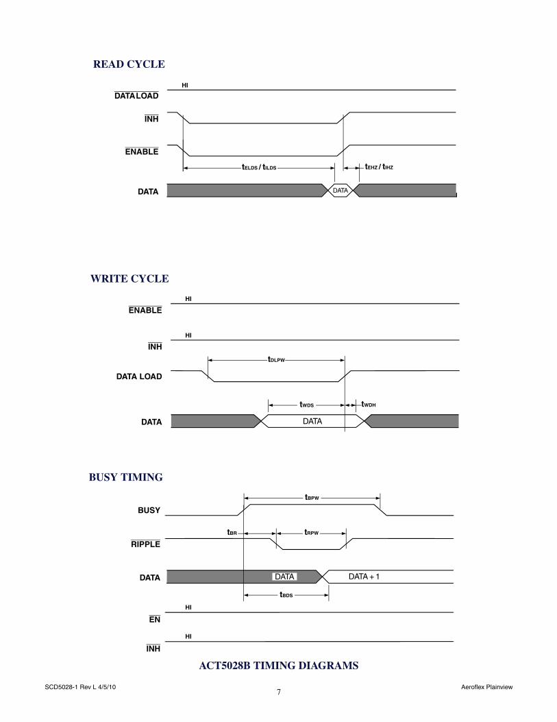
TIMING SPECIFICATIONS 6
DIGITAL OUTPUT SYM COMMENTS MIN TYP2 MAX UNITS
Busy tLH Rise Time - 20 85 ns
tHL Fall Time - 20 85 ns
CW/CCW, Ripple, B1- B16 tLH Rise Time - 45 100 ns
tHL Fall Time - 45 100 ns
Busy Pulse Width tBPW 300 400 600 ns
Busy to Data Stable 3 tBDS Enable = Low - - 350 ns
Ripple Pulse Width tRPW 160 200 300 ns
Busy to Ripple 3 tBR - 100 150 ns
READ DATA 3 (Enable & INH would normally be tied together, Data Load = Logic Hi)
Enable Low to D ata Stable tELDS - - 70 ns
Enable High to Data Hi-Z tEHZ - - 70 ns
INH Low to Data Stable tILDS - - 400 ns
INH High to Data Change tIHZ - - 150 ns
WRITING DATA 3 (Enable & INH = Logic Hi)
Data Load Pulse Width tDLPWTransparent Trailing Edge Latch 200 - - ns
Data Setup to Data Load tWDS 60 - - ns
Data Hold tWDH 10 - - ns
Notes1. @ 10 Bits, FREF > 4 x BWCL @ 12 Bits, FREF > 8 x BWCL @ 14 Bits, FREF > 12 x BWCL @ 16 Bits, FREF > 16 x BWCL2. All typical values are measured at +25°C.3. Characteristics are guaranteed by design, not production tested. 4. Accuracy apply over the full operating Power Supply voltage range, Full operating Temperature range, Reference Frequency range,
10% Signal Amplitude variation and 10% Reference Harmonic distortion.5. For ESD protection the ACT5028B features limiting resistors in series with diodes. Proper ESD precautions are strongly
recommended to avoid functional damage or performance degradation.6. All testing at nominal voltage.7. All unused inputs shall be tied to Ground. Bit 1 is always the MSB.
7SCD5028-1 Rev L 4/5/10 Aeroflex Plainview
DATA
DATA LOAD
ENABLE
tDLPW
tWDH
HI
READ CYCLE
DATA
INH
ENABLE
DATALOAD
tEHZ / tIHZtELDS / tILDS
HI
INHHI
tWDS
WRITE CYCLE
BUSY TIMING
DATA
BUSY
tBPW
tBDS
RIPPLE
tRPWtBR
ACT5028B TIMING DIAGRAMS
DATA
DATA
DATA DATA + 1
EN
INH
HI
HI

8SCD5028-1 Rev L 4/5/10 Aeroflex Plainview
FIG
UR
E 2
– A
CT
5028
B F
UN
CT
ION
AL
BL
OC
K D
IAG
RA
M DIG
ITA
L
OU
TP
UT
RE
SO
LVE
R
INP
UT
H=
1
EP
G1
[(S
/T)+
1]
S [
(S/1
0T)+
1]
Vco G2 S
VE
LOC
ITY
+
-
FIG
UR
E 3
– A
CT
5028
B T
RA
NSF
ER
FU
NC
TIO
N D
IAG
RA
M
- +
- +
ER
RO
R A
MP
+R
EF
-RE
F
R5
+5V
R6
C4
+2.
5V
C1
R1
R1
C2
C3
R2
C3
C2
R2
R3
+2.
25V
-
+
DIG
ITA
L
OU
TP
UT
16 B
ITU
P/D
OW
NC
OU
NT
ER
G=
2
CT
RE
SO
LVE
R
INP
UT
Cvc
o
20.5
p
Thr
esho
ld=
1.9
5V
G=
0.9
H=
1
G=
2G
=14
Vco
Vco
&T
IMIN
G
HY
ST
ER
ES
IS =
75n
A
AC1
BPF2
AC2
BPF1
DEMOD1
DEMOD2
INTIN2
INTIN1
INT1
INT2
CT
EG
DE
MO
D
CO
MP
100K
R4
100KR
4
.1µf
C1
.1µf
1413
151
611
1812
178
69
105

9SCD5028-1 Rev L 4/5/10 Aeroflex Plainview
-12dB/oct
G = 4
-6dB/oct
BW
2GGT
(T = G/2)
rad/sec10T
Closed Loop Bandwidth (BWcl) (Hz) =
-12dB/oct
2Gπ
--------------
FIGURE 4 – ACT5028B OPEN LOOP BODE PLOT
TRANSFER FUNCTION AND BODE PLOTThe dynamic performance of the converter can be determined from its Functional Block Diagram, TransferFunction Diagram and Bode plots, as shown in Figures 2, 3 and 4.
PROCEDURE FOR SELECTING RDC BANDWIDTH COMPONENTS *Input: Carrier Frequency (Fc) in Hz [47 to 30,000 Hz]Input: Nominal Resolver Input Level in Vrms [1Vrms min. to 1.5Vrms max.]Input: Resolution in bits; 10, 12, 14 or 16 bitsInput: Closed Loop Bandwidth (BWcl) in Hz [10 bit; BWcl = Fc/4 max.]
[12 bit; BWcl = Fc/8 max.][14 bit; BWcl = Fc/12 max.][16 bit; BWcl = Fc/16 max. ]
Input: Maximum Tracking Rate in RPS [16 bit; 16 RPS max.] (RPS = rotations per second) [14 bit, 64 RPS max.]
[12 bit; 256 RPS max.][10 bit, 1024 RPS max.]
Input: Hysteresis in LSBs. Recommended is 1 LSB for 16 & 14 bits and 0.7 LSBs for 12 & 10 bits.
EG = Nominal Resolver Input Level • .0027 [16 bit] orEG = Nominal Resolver Input Level • .011 [14 bit] orEG = Nominal Resolver Input Level • .043 [12 bit] orEG = Nominal Resolver Input Level • .17 [10 bit]G = 2.22 • BWcl
G2 = EG • 0.45 • G1 • G2
Hysteresis recommended valuesHYS = 0.7 [10 & 12 bit] orHYS = 1 [14 & 16 bit] or
R1(ohms) = 6 • 106 • EG • HYS
G2 = Maximum Tracking Rate • 215 [16 bit] orG2 = Maximum Tracking Rate • 213 [14 bit] orG2 = Maximum Tracking Rate • 211 [12 bit] orG2 = Maximum Tracking Rate • 29 [10 bit]R3(ohms) = (25 • 109)/G2
G1 = G2/(EG • .45 • G2)
BWcl

10SCD5028-1 Rev L 4/5/10 Aeroflex Plainview
C2(farads) = 1/(G1 • R1)
C3(farads) = C2/10
R2(ohms) = 2/(G • C2)
ACT5028B EXAMPLE CALCULATIONSCarrier Frequency = 800 HzNominal Resolver Input Level = 1.3VrmsResolution = 14 bitsClosed Loop Bandwidth (BWcl) = 20 HzMaximum Tracking Rate in RPS = 1Hysteresis = 1 LSB
EG = Nominal Resolver Input Level • .011 [14 bit] = 1.3 • .011 = .014G = 2.22 • BWcl = 2.22 • 20 = 44.4HYS = 1 [14 bit]R1(ohms) = 6 • 106 • EG • HYS = 6 • 106 • .014 • 1 = 84K. Use closest standard resistor = 84.5K 1%
G2 = Maximum Tracking Rate • 213 = 8192 [213 for 14 bits]R3(ohms) = (25 • 109)/G2 = (25 • 109)/8192 = 3,050K. Use closest standard resistor = 3.01M 1% or 3M 5%
G2 = EG • 0.45 • G1 • G2G1 = G2/(EG • .45 • G2) = 44.42/(.014 • .45 • 8192) = 38.2C2(farads) = 1/(G1 • R1) = 1/(38.2 • 84.5K) = .31µF. Use closest standard capacitor = .33µF 10%C3 = C2/10(farads) = C2/10 = .33µ/10 = .033µFR2(ohms) = 2/(G • C2) = 2/(44.4 • .33µ) = 136.5K. Use closest standard resistor = 137K 1%
SIGNAL AND REFERENCE INPUT CONDITIONINGInputs to the converter should be 1.3 Vrms nominal, resolver format referenced to VCC/2 nominal Figure 5shows various input configurations.
REFERENCE CONDITIONINGMost resolvers have a LEADING input to output phase shift. A simple C-R leading phase shift network(Figure 5 – Reference Conditioning) from the resolver reference to the RDC’s reference input will providethe compensating phase shift required to bring the signals in phase. If the resolver has a LAGGING inputto output phase shift an R-C lagging phase shift network (low pass network) would be required.
Note the C-R phase lead circuit on the input to the Demodulator (BPF1 and BPF2) in Figure 2 should beconsidered when calculating the total system phase compensation.
The formula for calculating the phase shift network is as follows:
1 Phase angle = ArcTan 6.28 x (R7 + R8) x C FREF
Select a convenient capacitor value and perform the following calculation to determine the proper resistorvalue.
R = 1 (Tan (Phase Angle)) x FREF x 6.28 x C
* Software Program SW5028-2 available at Aeroflex WEB site.

11SCD5028-1 Rev L 4/5/10 Aeroflex Plainview
FIG
UR
E 5
– A
CT
5028
B R
ESO
LVE
R, S
YN
CH
RO
AN
D R
EF
ER
EN
CE
IN
PU
T C
ON
FIG
UR
AT
ION
S
x x
+S
IN
-SIN
+C
OS
-CO
S
VC
C/2
x x
y y
+S
INx
+S
IN
y
-SIN
x-S
IN
y
+C
OS
x
+C
OS
y
-CO
Sx
-CO
S
y
S3
x
+S
IN
y
x-S
IN
y
x/2
+C
OS
z
z =
x (
sq r
t 3)
-CO
S
z
S1
S2
xx
10K
+5V
10K
.1µF
R8
+R
EF
-RE
F
+R
EF
+R
EF
C5
+R
EF
+R
EF
-RE
F-R
EF
DIR
EC
T R
ESO
LVE
RSI
NG
LE
EN
DE
D R
ESO
LVE
RC
ON
DIT
ION
ING
DIF
FE
RE
NT
IAL
RE
SOLV
ER
CO
ND
ITIO
NIN
GSY
NC
HR
O C
ON
DIT
ION
ING
2.5V
DC
SIN
GL
E E
ND
ED
RE
FE
RE
NC
ED
IFF
ER
EN
TIA
L R
EF
ER
EN
CE
CO
ND
ITIO
NIN
G(F
LO
AT
ING
RE
FE
RE
NC
E)
+S
IN
-SIN
+C
OS
-CO
S
+S
IN
-SIN
+C
OS
-CO
S
+S
IN
-SIN
+C
OS
-CO
S
CO
ND
ITIO
NIN
G
VC
C/2
VC
C/2
VC
C/2
VC
C/2
VC
C/2
VC
C/2
VC
C/2
VC
C/2
VC
C/2
4.7µ
F
R7
R8
C5
R7
R8
C5
R7
+

12SCD5028-1 Rev L 4/5/10 Aeroflex Plainview
Reading the ACT 5028B
The Busy signal is asynchronous to the Read signal created by the interface circuit that reads it. Because of theasynchronous nature of the system (inherent with other Resolver to Digital Converters) the designer must be carefulwhen reading the digital interface.
The implementation of reading the RDC is accomplished in one of two ways, using a CPU/MPU or using an FPGA.The best method for reading the counter may also depend on the rep rate of the counter clock that can vary from 0 to1µS.
The Busy pulse is instrumental in reading stable data from the ACT5028. The Busy pulse will be present for thefollowing two situations:
1) When ever data is incremented or decremented in the RDC counter.
2) Directly after the trailing positive going edge of /INH (see A within example 5 timing diagram).
Based on 1 above there are many methods that can be implemented to synchronize the reading of data from theACT5028, below are a few examples:
Example 1: If the only time a read will occur is after the RDC has stopped (0 rps) there will be no Busy signalto contend with.
Example 2: Knowing the Busy rep rate an Interrupt to a CPU or Logic can be developed from the Busy pulsefor the system to Read the RDC chip as long as the read is guaranteed to occur prior to the nextBusy pulse.
Example 3: As long as the resolver is rotating the Busy Pulse can be used to indicate stable data to be
sampled on leading or trailing edge.
Example 4: Ignore Busy and perform two reads back to back and compare, if they are equal you have gooddata. The designer should be aware of the rep rate of Busy which is equal to the clock rate of thecounter. In most cases the angular velocity is < 3 rps in which case with a 16 bit counter rep ratewould be (1 / 216 * 3) 5µS. In this situation the reads would like to be within 5µs of each otherand the LSB would be ignored. Although this method would be easier to implement with a CPUit could also be done in an FPGA.
Example 5: The circuit below ignores the Busy signal but insures sampling of stable data. The clock shouldbe a least 10MHz, the /RD pulse should be a minimum of 1.2µs (to insure minimum /INH pulsewidth of 400ns), the sampling of data should be taken on the rising edge of the signal /RD. The/RD signal is synced up with the CLK such that the sampling on the D latch occurs on theopposite edge of the /RD transition.
/INH & /EN
Busy Q
/Q
D
CKCLK
Q
/Q
D
CK
/RD
S
S
EXAMPLE 5 CIRCUIT

13SCD5028-1 Rev L 4/5/10 Aeroflex Plainview
CLK
Busy
/INH & /EN
/RD
tBPW
A
CLK
Busy
/INH & /EN
/RD
100ns
1.2µs - 50ns
A1.2 µs
1.2 µs
1.2µs - tBPW - 50ns
Busy occurs around Leading edge of /RD
Busy occurs @ Positive edge of CLK with /RD low
100ns
EXAMPLE 5 CIRCUIT TIMING WAVEFORMS

14SCD5028-1 Rev L 4/5/10 Aeroflex Plainview
TABLE I – ACT5028B PIN OUT DESCRIPTIONS (CQFP PACKAGE)
PIN # FUNCTION PIN # FUNCTION PIN # FUNCTION
1 DATA LOAD 19 A GND 37 BIT 9
2 VL I/O 20 N/C 38 BIT 10
3 A GND 21 -SIN 39 BIT 11
4 A +5V 22 +SIN 40 BIT 12
5 VCOIN 23 A GND 41 BIT 13
6 INTIN2 24 -COS 42 BIT 14
7 N/C 25 +COS 43 BIT 15
8 INTIN1 26 D GND 44 BIT 16 (LSB)
9 INT1 27 D +5V 45 ENABLE
10 INT2 28 BIT 1 (MSB) 46 N/C
11 +REF 29 BIT 2 47 INH
12 -REF 30 BIT 3 48 SC2
13 AC2 31 BIT 4 49 SC1
14 AC1 32 BIT 5 50 BUSY
15 BPF2 33 N/C 51 CW/CCW
16 BPF1 34 BIT 6 52 RIPPLE
17 DEMOD1 35 BIT 7
18 DEMOD2 36 BIT 8

15SCD5028-1 Rev L 4/5/10 Aeroflex Plainview
.956 SQMAX
.600±.005
.050.023TYPTYP
.017TYP
.250
.008
.005
.063±.007
.008REF
.100MAX
34
46
47
1
7
8
3321
20
+.02-0
FIGURE 6 – 52 PIN CERAMIC QUAD FLAT PACKAGE (CQFP) OUTLINE

16SCD5028-1 Rev L 4/5/10 Aeroflex Plainview
ERRATA INFORMATION ACT5028-2-X-X
This Errata information represents the known bugs, anomalies, and work-arounds for the ACT5028 Resolver to DigitalConverter
DESCRIPTION OF ANOMALIES:
Anomaly #1: Instability at 360o and 180o Input Angles
Anomaly #2: Correcting for the Integral Nonlinearity Error found in Revision B Silicon
Anomaly #3: Precautionary note when power is first applied.
EFFECTED PARTS:
ANOMALY #1
PROBLEM DESCRIPTION:This problem occurs in the 16 Bit mode when rotating in the clockwise (CW) direction and has been observed on100% of the parts tested at 25°C. It occurs 100% of the time at 360o and approximately 76% at 180o. At 360o theproblem occurs when the counter passes from FFFF to 0000 then reverse rotation (CCW) back to FFFF. At 180o theproblem occurs when the counter passes from 7FFF to 8000 then reverse rotation (CCW) back to 7FFF.
Two different failure modes have been observed:
1) The output latch locks to a value with the MSB inverted giving the indication that the RDC chip is 180o out of phase, the RDC chip exhibits zero error. This condition remains indefinitely until the resolver rotates in
either direction by one count. At which time the RDC chip responds to the 180o error which takes less than 150ms to correct.
2) The RDC chip sees an immediate error of 180o and begins to correct for this error which takes less than 150ms.
In some cases it has been observed that the MSB is OK but the next bit gets inverted which provides a 90o error. In thiscase the time required for the RDC chip to correct its self is less than 75 ms.
RECOMMENDED ACTIONS:1) Use the 10 or 12 Bit mode where this problem doesn’t exist. Note: The 14 bit mode will also work using the
Aeroflex part numbers over the temperature ranges shown below:
2) Insure a hysteresis of at least one bit to prevent this anomaly when rotating very slowly.
3) Avoid reversing direction at 360o and 180o when rotating in the CW direction.
4) If the resolver stops within two counts of 360o or 180o wait 150ms after motion resumes before reading the RDC output.
Model Anomaly Anomaly Anomaly
ACT5028-2-1-X 1 2a 3
ACT5028-2-2-X 1 2b 3
ACT5028-2-1-S -55°C to +125°C
ACT5028-2-2-S -40°C to +125°C

17SCD5028-1 Rev L 4/5/10 Aeroflex Plainview
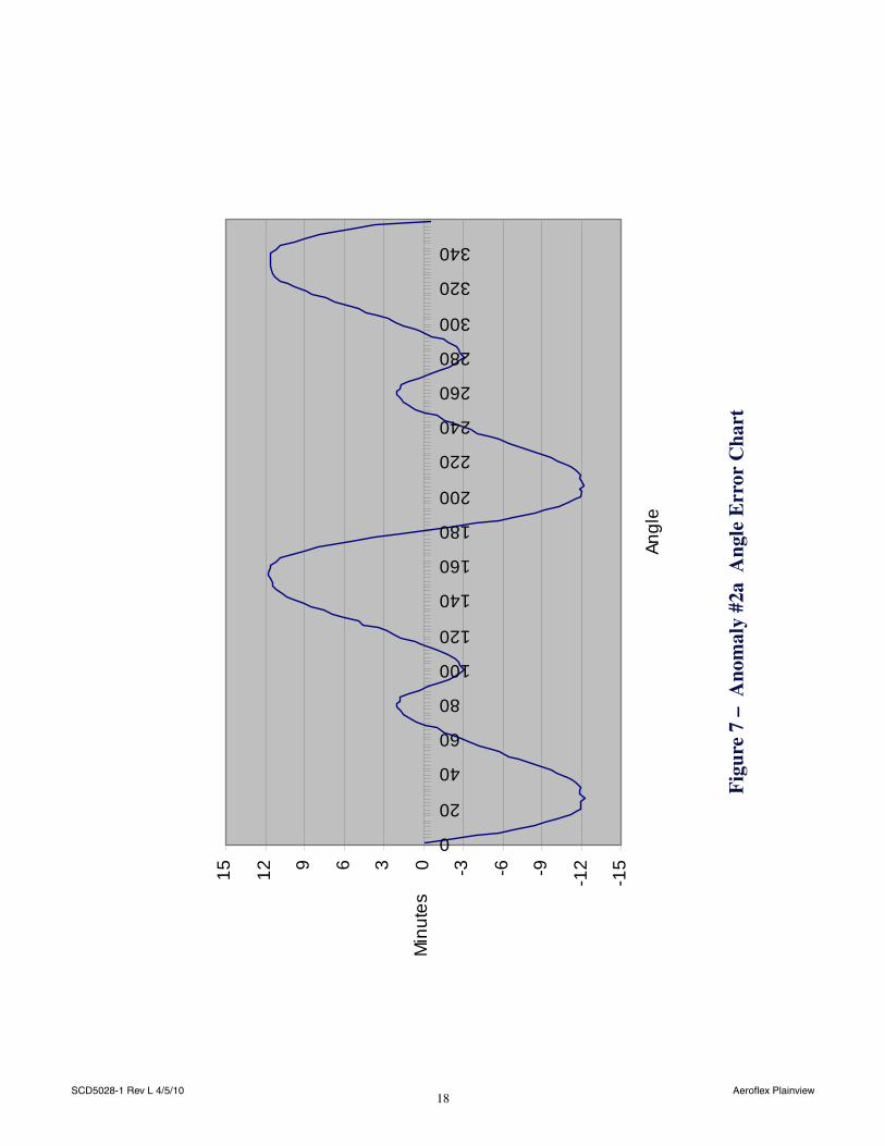
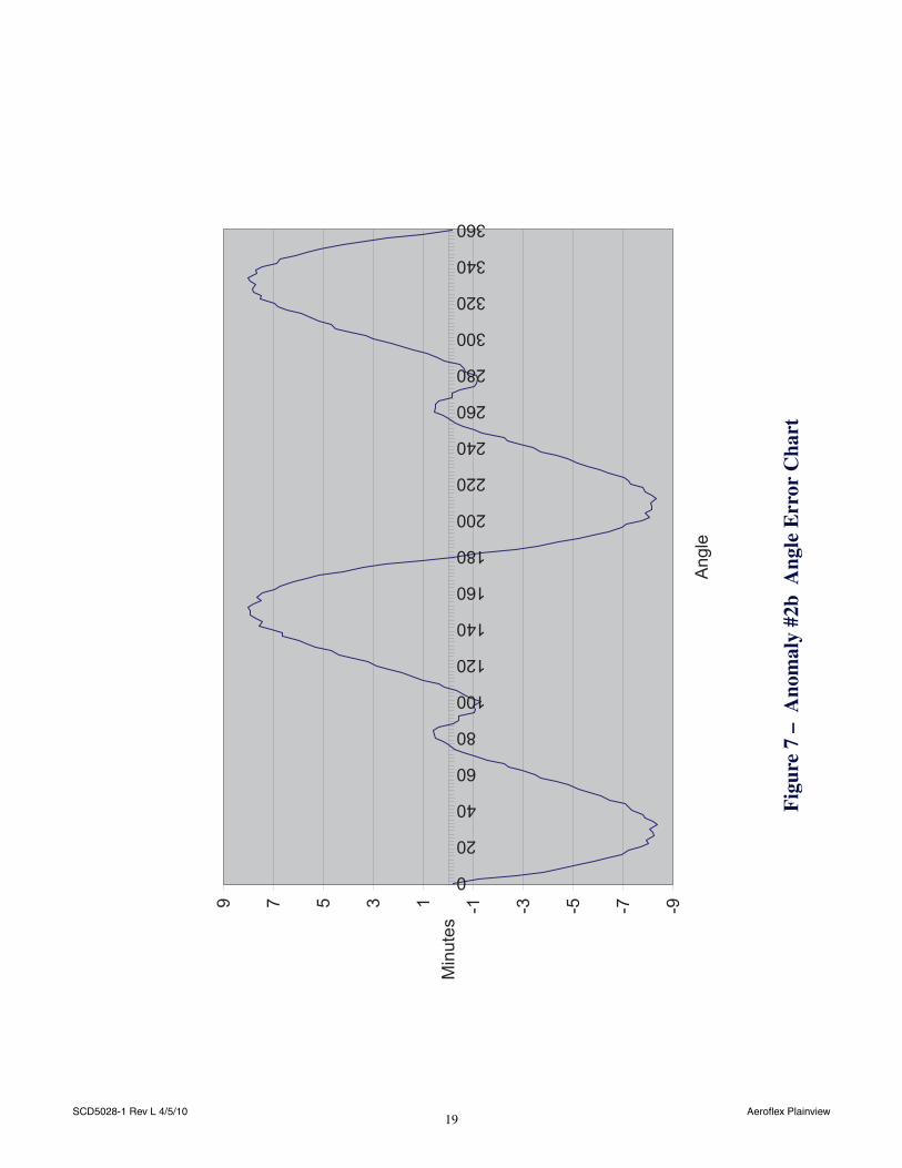
ANOMALY #2
PROBLEM DESCRIPTION AND RECOMMENDED ACTION:This Errata information is to address the constant Integral Nonlinearity (INL) that exists at each angle of theACT5028B Resolver to Digital Converter (RDC). This error is repeatable from chip to chip and provides a look upTable of offsets that must be added to the output of the Resolver to Digital Converter to get the correct angle.
Figure 7 shows the error in Minutes that exists at 2o increments for the full 360o. Note that the INL error from 0o to180o is basically the same as the error between 180o and 360o. Table II has the angle and correction factor (in Minutes)that must be added to zero out the INL error.
A simple calculation can be performed to derive a correction factor for angles that fall between the angles listed inTable II herein.
AL = Larger Angle
AS = Smaller Angle
CL = Correction Factor associated with larger Angle
CS = Correction Factor associated with smaller Angle
NA = New Angle
NCF = New Correction Factor
Formula: NCF = CS + (((NA - AS) / (AL - AS)) * (CL - CS))
Example:
Require the correction factor @ 15o
NCF = 10.17114258 + (((15 – 14) / (16 – 14)) * (11.11376953 - 10.17114258))
NCF = 10.17114258 + (((1) / (2)) * .94262695)
NCF = 10.17114258 + (.5 * .94262695)
NCF = 10.17114258 + .471313475
NCF = 10.64245606 minutes
18SCD5028-1 Rev L 4/5/10 Aeroflex Plainview
-15
-12-9-6-303691215
0
20
40
60
80
100
120
140
160
180
200
220
240
260
280
300
320
340
Angl
e
Min
utes
Fig
ure
7 –
Ano
mal
y #2
a A
ngle
Err
or C
hart
19SCD5028-1 Rev L 4/5/10 Aeroflex Plainview
-9-7-5-3-113579
0
20
40
60
80
100
120
140
160
180
200
220
240
260
280
300
320
340
360
Ang
le
Min
utes
Fig
ure
7 –
Ano
mal
y #2
b A
ngle
Err
or C
hart

20SCD5028-1 Rev L 4/5/10 Aeroflex Plainview
Angle CorrectionFactor Angle Correction
Factor Angle Correction Factor Angle Correction
Factor
0 0.125244141 90 0.415283203 180 0.145019531 270 0.4746093752 1.911621094 92 1.153564453 182 1.997314453 272 1.2062988284 4.073730469 94 1.977539062 184 3.981445312 274 1.9709472666 5.715087891 96 2.537841797 186 5.754638672 276 2.5773925788 6.868652344 98 2.814697266 188 6.822509766 278 2.64990234410 8.411132812 100 3.071777344 190 8.411132813 280 3.15087890612 9.241699219 102 2.735595703 192 9.221923828 282 2.79492187514 10.17114258 104 2.656494141 194 10.19750977 284 2.68286132816 11.11376953 106 2.478515625 196 11.09399414 286 2.56420898418 11.54882812 108 1.885253906 198 11.44995117 288 1.85888671920 11.94433594 110 1.285400391 200 11.97729492 290 1.56225585922 11.99707031 112 0.837158203 202 12.01025391 292 0.62622070324 11.91137695 114 -0.243896484 204 11.88500977 294 -0.17138671926 12.26733398 116 -0.626220703 206 12.19482422 296 -0.65258789128 11.85205078 118 -1.621582031 208 12.10913086 298 -1.49633789130 11.77954102 120 -2.168701172 210 11.82568359 300 -2.08300781232 11.97070312 122 -2.814697266 212 11.92456055 302 -2.64990234434 11.64770508 124 -3.460693359 214 11.64111328 304 -3.61889648436 11.26538086 126 -4.548339844 216 11.22583008 306 -4.40332031338 10.90942383 128 -4.871337891 218 10.89624023 308 -4.9570312540 10.16455078 130 -5.945800781 220 10.13818359 310 -5.87988281242 9.683349609 132 -6.842285156 222 9.650390625 312 -6.72363281344 9.030761719 134 -7.48828125 224 8.984619141 314 -7.46191406346 8.002441406 136 -8.582519531 226 7.969482422 316 -8.45068359448 7.237792969 138 -9.043945313 228 7.218017578 318 -8.91870117250 6.545654297 140 -9.887695313 230 6.492919922 320 -9.75585937552 5.6953125 142 -10.31616211 232 5.682128906 322 -10.2963867254 5.174560547 144 -10.73144531 234 5.174560547 324 -10.8105468756 4.198974609 146 -11.15332031 236 4.185791016 326 -11.2917480558 3.487060547 148 -11.43017578 238 3.520019531 328 -11.397216860 2.939941406 150 -11.32470703 240 2.887207031 330 -11.4499511762 2.241210938 152 -11.64770508 242 2.181884766 332 -11.5751953164 1.614990234 154 -11.70043945 244 1.588623047 334 -11.6542968866 1.087646484 156 -11.71362305 246 1.114013672 336 -11.6279296968 0.131835938 158 -11.5949707 248 0.171386719 338 -11.6279296970 -0.547119141 160 -11.58837891 250 -0.573486328 340 -11.5620117272 -1.0546875 162 -11.1862793 252 -1.074462891 342 -11.1203613374 -1.549072266 164 -10.79077148 254 -1.502929687 344 -10.8171386776 -1.641357422 166 -9.861328125 256 -1.628173828 346 -9.83496093878 -1.977539063 168 -8.971435547 258 -1.984130859 348 -8.97802734480 -1.944580078 170 -7.929931641 260 -1.957763672 350 -7.88378906382 -1.766601563 172 -6.512695313 262 -1.713867188 352 -6.47314453184 -1.753417969 174 -5.510742187 264 -1.694091797 354 -5.44482421986 -1.0546875 176 -3.697998047 266 -1.034912109 356 -3.68481445388 -0.250488281 178 -1.680908203 268 -0.283447266 358 -1.654541016
Table II – Anomaly #2a Correction Factor (Minutes)

21SCD5028-1 Rev L 4/5/10 Aeroflex Plainview
Angle CorrectionFactor Angle Correction
Factor Angle Correction Factor Angle Correction
Factor
0 0.203780402 90 0.388943965 180 0.192649156 270 0.1494676332 1.201123493 92 0.425014547 182 1.302393729 272 0.4663943334 2.70465535 94 1.029048142 184 2.654324654 274 1.0246463116 3.789635076 96 1.054983614 186 3.541737941 276 1.1382953648 4.421013418 98 0.985566018 188 4.412445369 278 1.1587671710 5.215566619 100 1.304993369 190 5.203491983 280 1.09992344412 5.834478943 102 0.905201887 192 5.803723899 282 0.69427606114 6.365571511 104 0.618766526 194 6.389561265 284 0.63483576116 6.955572794 106 0.339237225 196 6.917655625 286 0.44544979718 7.215013746 108 -0.175559243 198 7.108442088 288 -0.17721475420 7.668033013 110 -0.406551233 200 7.718946308 290 -0.45471820922 8.020721684 112 -0.99953425 202 8.027522848 292 -0.88949264724 7.933794161 114 -1.499164395 204 7.888002744 294 -1.40342139426 8.232306488 116 -1.844624191 206 8.144939892 296 -1.84368497628 8.178317924 118 -2.397679189 208 8.138785463 298 -2.29349536130 8.045994542 120 -2.881543541 210 8.080969999 300 -3.02874494332 8.36259965 122 -3.236345202 212 8.292840379 302 -3.32441037134 8.165615526 124 -3.826772691 214 8.137597002 304 -3.9562293236 7.853648573 126 -4.402200107 216 7.853112414 306 -4.50910332738 7.801531535 128 -4.684869835 218 7.773708404 308 -4.68870363840 7.335965753 130 -5.328598278 220 7.275534799 310 -5.18704553942 7.221900549 132 -5.670542709 222 7.201587126 312 -5.50926272544 7.082034482 134 -5.97411451 224 7.004955442 314 -5.88837965246 6.460299345 136 -6.658819257 226 6.398031462 316 -6.4806659748 6.09360404 138 -6.661897423 228 6.026752907 318 -6.81428469750 5.627097169 140 -7.094021917 230 5.558449327 320 -6.98052374752 5.225444131 142 -7.603145351 232 5.165559731 322 -7.52534438954 4.799049593 144 -7.4361178 234 4.774337917 324 -7.47530574656 4.331451914 146 -7.735451293 236 4.300501478 326 -7.83046316958 3.692843475 148 -7.941762029 238 3.67712898 328 -7.84508526760 3.461690092 150 -7.955998624 240 3.376174401 330 -7.73720937262 2.917592224 152 -8.046982441 242 2.842718999 332 -7.95010611164 2.396542424 154 -7.80890584 244 2.361198081 334 -8.02312206866 2.206561334 156 -7.518632897 246 2.219187977 336 -7.69054597468 1.553478755 158 -7.694354839 248 1.317468789 338 -7.7190865470 1.049330378 160 -7.452276395 250 1.026060671 340 -7.43801366872 0.597675735 162 -6.973083459 252 0.584687534 342 -6.89599836974 0.206092961 164 -6.72826432 254 0.257365342 344 -6.75976131176 0.019981548 166 -6.191360248 256 0.024375455 346 -6.14172147978 -0.219060483 168 -5.698378367 258 -0.199283218 348 -5.69708799180 -0.546519868 170 -5.196077543 260 -0.576187854 350 -5.13295633982 -0.576407731 172 -4.228528382 262 -0.534840477 352 -4.2030930884 -0.614729518 174 -3.402853297 264 -0.531974122 354 -3.33512029886 -0.399630686 176 -2.508137965 266 -0.387924935 356 -2.45357083688 0.180584177 178 -1.065912708 268 0.143590373 358 -1.041202907
Table II – Anomaly #2b Correction Factor (Minutes)

22SCD5028-1 Rev L 4/5/10 Aeroflex Plainview
ANOMALY #3
PRECAUTIONARY NOTE:The ACT5028 RDC converter can provide incorrect data output if a unit step of 180° (starting at any angle)is introduced to the Sin / Cos input. This anomaly is difficult to reproduce since a Resolver will never provide a unit step function to the RDCchip. The only time this would be a concern is during power up, if the Resolver is set to 180°. The RDC willinitialize its internal counter to 0000h which simulates the unit step function mentioned above. In practicethis error condition during power up is difficult to produce because of the dynamics associated with all thevariables when power is first applied. If the system designer does nothing to accommodate this potential problem the system could see an error atpower on, however, this error will be self corrected once the Resolver begins to rotate.

SCD5028-1 Rev L 4/5/1023
PLAINVIEW, NEW YORKToll Free: 800-THE-1553 Fax: 516-694-6715
SE AND MID-ATLANTIC Tel: 321-951-4164 Fax: 321-951-4254
INTERNATIONALTel: 805-778-9229Fax: 805-778-1980
WEST COAST Tel: 949-362-2260Fax: 949-362-2266
NORTHEASTTel: 603-888-3975Fax: 603-888-4585
CENTRALTel: 719-594-8017Fax: 719-594-8468
w w w . a e r o f l e x . c o m i n f o - a m s @ a e r o f l e x . c o m
Aeroflex Microelectronic Solutions reserves the right to change at any time without notice the specifications, design, function, or form of its products described herein. All parameters must be validated for each customer's application by engineering. No liability is assumed as a result of use of this product. No patent licenses are implied.
Our passion for performance is defined by threeattributes represented by these three icons:solution-minded, performance-driven and customer-focused
EXPORT CONTROL: EXPORT WARNING:This product is controlled for export under the International Traffic inArms Regulations (ITAR). A license from the U.S. Department ofState is required prior to the export of this product from the UnitedStates.
Aeroflex’s military and space products are controlled for export underthe International Traffic in Arms Regulations (ITAR) and may not besold or proposed or offered for sale to certain countries. (See ITAR126.1 for complete information.)
ORDERING INFORMATION 3
AEROFLEX PART # DSCC SMD # SCREENING PACKAGE
ACT5028-201-1SACT5028-201-2S
5962-0423501KXC5962-0423501KXA
In accordance with DSCC SMD Rev. B Silicon2
CQFP-
ACT5028-202-1SACT5028-202-2S
5962-0423502KXC5962-0423502KXA
ACT5028-2-1-S 1 - Class K, Rev. B Silicon2
ACT5028-2-1-7 1 Class C, Rev. B Silicon2
ACT5028-2-2-S 1 - -
Class K, Rev. B Silicon2
ACT5028-2-2-7 1 Class C, Rev. B Silicon2
ACT5028, Evaluation board 3 4 -
Notes1. Dash #’s: The first dash number indicates the revision of silicon: -1 = Rev. A -2 = Rev. B The second dash number indicates the wafer lot run. The last dash number indicates the testing level of the part: 7 = Class C = Commercial Flow, Commercial Temp. Range, 0oC to +70oC testing S = MIL-PRF-38534 Class K Flow, -55oC to +125oC testing (Rev. B Silicon)2. See Errata information Anomaly #1, 2 & 3 within this data sheet.3. Contact factory for availability and pricing.4. See Application note AN5028-1