ad1376/ad1377 complete, high speed 16-bit a/d … · complete, high speed 16-bit a/d converters ......
TRANSCRIPT

Complete, High Speed16-Bit A/D Converters
AD1376/AD1377
Rev. D Information furnished by Analog Devices is believed to be accurate and reliable. However, no responsibility is assumed by Analog Devices for its use, nor for any infringements of patents or other rights of third parties that may result from its use. Specifications subject to change without notice. No license is granted by implication or otherwise under any patent or patent rights of Analog Devices. Trademarks and registered trademarks are the property of their respective owners.
One Technology Way, P.O. Box 9106, Norwood, MA 02062-9106, U.S.A. Tel: 781.329.4700 www.analog.com Fax: 781.481.3113 © 2005 Analog Devices, Inc. All rights reserved.
FEATURES Complete 16-bit converters with reference and clock ±0.003% maximum nonlinearity No missing codes to 14 bits over temperature Fast conversion
17 µs to 16 bits (AD1376) 10 µs to 16 bits (AD1377)
Short cycle capability Adjustable clock rate Parallel outputs Low power
645 mW typical (AD1376) 585 mW typical (AD1377)
Industry-standard pinout
GENERAL DESCRIPTION The AD1376/AD1377 are high resolution, 16-bit analog-to-digital converters with internal reference, clock, and laser-trimmed thin-film applications resistors. The AD1376/AD1377 are excellent for use in high resolution applications requiring moderate speed and high accuracy or stability over commercial temperature ranges (0°C to 70°C). They are packaged in compact 32-lead, ceramic seam-sealed (hermetic), dual in-line packages (DIP). Thin-film scaling resistors provide bipolar input ranges of ±2.5 V, ±5 V, and ±10 V and unipolar input ranges of 0 V to +5 V, 0 V to +10 V, and 0 V to +20 V.
Digital output data is provided in parallel form with corresponding clock and status outputs. All digital inputs and outputs are TTL-compatible.
For the AD1376, the serial output function is no longer available after date code 0111. For the AD1377, the serial output function is no longer available after date code 0210. The option of applying an external clock on the CONVERT START pin to slow down the internally set conversion time is no longer supported for either part.
PRODUCT HIGHLIGHTS
1. The AD1376/AD1377 provide 16-bit resolution with a maximum linearity error of ±0.003% (1/2 LSB14) at 25°C.
2. The AD1376 conversion time is 14 µs (typical) short cycled to 14 bits, and 16 µs to 16 bits.
3. The AD1377 conversion time is 8 µs (typical) short cycled to 14 bits, and 9 µs to 16 bits.
4. Two binary codes are available on the digital output. They are CSB (complementary straight binary) for unipolar input voltage ranges and COB (complementary offset binary) for bipolar input ranges. Complementary twos complement (CTC) coding may be obtained by inverting Pin 1 (MSB).
5. The AD1376/AD1377 include internal reference and clock with external clock rate adjust pin, and parallel digital outputs.
FUNCTIONAL BLOCK DIAGRAM
0069
9-00
1
(MSB) BIT 1 1
BIT 2 2
BIT 3 3
BIT 4 4
BIT 5 5
BIT 6 6
BIT 7 7
BIT 8 8
BIT 9 9
BIT 10 10
BIT 11 11
BIT 12 12
(LSB FOR 13 BITS) BIT 13 13
(LSB FOR 14 BITS) BIT 14 14
BIT 15 15
BIT 16 16
SHORT CYCLE32
CONVERT START31
+5V DC SUPPLY VL30
GAIN ADJUST29
+15V DC SUPPLY VCC28
COMPARATOR IN27
BIPOLAR OFFSET26
+10V25
+20V24
CLK RATE CTRL23
ANALOG COMMON22
–15V DC SUPPLY VEE21
CLOCK OUT20
DIGITAL COMMON19
STATUS18
NC17
16-B
IT D
AC
16-BIT SAR
CLOCK
REFERENCE
COMPARATOR
7.5kΩ
3.75kΩ 3.75kΩ
AD1376/AD1377
Figure 1.

AD1376/AD1377
Rev. D | Page 2 of 12
TABLE OF CONTENTS Specifications..................................................................................... 3
Absolute Maximum Ratings............................................................ 5
ESD Caution.................................................................................. 5
Description of Operation ................................................................ 6
Gain Adjustment .......................................................................... 6
Zero Offset Adjustment............................................................... 6
Timing............................................................................................ 7
Digital Output Data ..................................................................... 7
Input Scaling ..................................................................................7
Calibration (14-Bit Resolution Examples) .................................8
Grounding, Decoupling, and Layout Considerations ..............9
Clock Rate Control........................................................................9
High Resolution Data Acquisition System.............................. 10
Applications..................................................................................... 11
Outline Dimensions ....................................................................... 12
Ordering Guide .......................................................................... 12
REVISION HISTORY
6/05—Rev. C to Rev. D Updated Format..................................................................Universal Updated Outline Dimensions ....................................................... 12
6/03—Rev. B to Rev. C Removed Serial Output Function and Adjustable Clock Rate ........................................................Universal Updated Format..................................................................Universal Changes to General Description .................................................... 1 Changes to Product Highlights....................................................... 1 Changes to Functional Block Diagram.......................................... 1 Inserted ESD Warning ..................................................................... 3 Change to Ordering Guide.............................................................. 3 Change to Figure 7 ........................................................................... 5 Deleted text from Digital Output Data.......................................... 5 Deleted Figure 9 and Renumbered Remainder of Figures.......... 5 Deleted the ‘Using the AD1376 or AD1377 at Slower Conversion Times’ Section............................................... 8 Deleted Figure 16.............................................................................. 8 Change to Figure 13 ......................................................................... 9 Change to Figure 14 ......................................................................... 9 Updated Outline Dimensions ....................................................... 10

AD1376/AD1377
Rev. D | Page 3 of 12
SPECIFICATIONS Typical at TA = 25°C, VS = ±15 V, +5 V, unless otherwise noted.
Table 1. AD1376JD/AD1377JD AD1376KD/AD1377KD Model Min Typ Max Min Typ Max Unit RESOLUTION 16 16 Bits ANALOG INPUTS
Voltage Ranges Bipolar ±2.5 ±2.5 V ±5 ±5 V ±10 ±10 V Unipolar 0 to 5 0 to 5 V
0 to 10 0 to 10 V 0 to 20 0 to 20 V Impedance (Direct Input) V
0 V to +5 V, ±2.5 V 1.88 1.88 kΩ 0 V to +10 V, ±5.0 V 3.75 3.75 kΩ 0 V to +20 V, ±10 V 7.50 7.50 kΩ
DIGITAL INPUTS1 Convert Command Trailing edge of positive 50 ns (min) pulse Logic Loading 1 1 LS TTL Load
TRANSFER CHARACTERISTICS2 (ACCURACY)
Gain Error ±0.053 ±0.2 ± 0.053 ± 0.2 % Offset Error
Unipolar ±0.053 ±0.1 ±0.053 ±0.1 % of FSR4
Bipolar ±0.053 ±0.2 ±0.053 ±0.2 % of FSR Linearity Error (Max) ±0.006 ±0.003 % of FSR Inherent Quantization Error ±1/2 ±1/2 LSB Differential Linearity Error ±0.003 ±0.003 % of FSR
POWER SUPPLY SENSITIVITY ±15 V DC (±0.75 V) 0.0015 0.0015 % of FSR/% ∆VS
+5 V DC (±0.25 V) 0.001 0.001 % of FSR/% ∆VS
CONVERSION TIME5 12 Bits (AD1376) 11.5 13 11.5 13 µs 14 Bits (AD1376) 13.5 15 13.5 15 µs 16 Bits (AD1376) 15.5 17 15.5 17 µs 14 Bits (AD1377) 8.75 8.75 µs 16 Bits (AD1377) 10 10 µs
POWER SUPPLY REQUIREMENTS Analog Supplies +14.5 +15 +15.5 +14.5 +15 +15.5 V dc −14.5 −15 −15.5 −14.5 −15 −15.5 V dc Digital Supply +4.75 +5 +5.25 +4.75 +5 +5.25 V dc AD1376 Power Consumption 600 800 600 800 mW
+15 V Supply Drain +10 +10 mA −15 V Supply Drain −23 −23 mA +5 V Supply Drain +18 +18 mA
AD1377 Power Consumption 600 800 600 800 mW +15 V Supply Drain +10 +10 mA −15 V Supply Drain −23 −23 mA +5 V Supply Drain +18 +18 mA
WARM-UP TIME 1 1 Minutes

AD1376/AD1377
Rev. D | Page 4 of 12
AD1376JD/AD1377JD AD1376KD/AD1377KD Model Min Typ Max Min Typ Max Unit DRIFT6
Gain ±15 ±5 ±15 ppm/°C Offset
Unipolar ±2 ±4 ±2 ±4 ppm of FSR/°C Bipolar ±10 ±3 ±10 ppm of FSR/°C
Linearity ±2 ±3 ±0.3 ±2 ppm of FSR/°C Guaranteed No Missing Code
Temperature Range 0 to 70 (13 Bits) 0 to 70 (14 Bits) °C DIGITAL OUTPUT1
(All Codes Complementary) Parallel Output Codes7
Unipolar CSB CSB Bipolar COB, CTC8 COB, CTC8 Output Drive 5 5 LSTTL Loads
Status Logic 1 During Conversion
Logic 1 During Conversion
Status Output Drive 5 5 LSTTL Loads Internal Clock9
Clock Output Drive 5 5 LSTTL Loads Frequency 1040/1750 1040/1750 kHz
TEMPERATURE RANGE Specification 0 to 70 0 to 70 °C Operating −25 to +85 −25 to +85 °C Storage −55 to +125 −55 to +125 °C
1 Logic 0 = 0.8 V max; Logic 1 = 2.0 V min for inputs. For digital outputs, Logic 0 = 0.4 V max. Logic 1 = 2.4 V min. 2 Tested on ±10 V and 0 V to +10 V ranges. 3 Adjustable to zero. 4 Full-scale range. 5 Conversion time may be shortened with “short cycle” set for lower resolution. 6 Guaranteed but not 100% production tested. 7 CSB–Complementary Straight Binary. COB–Complementary Offset Binary. CTC–Complementary Twos Complement. 8 CTC coding obtained by inverting MSB (Pin 1). 9 With Pin 23, clock rate controls tied to digital ground.
AD1376/AD1377
Rev. D | Page 5 of 12
ABSOLUTE MAXIMUM RATINGS
Table 2. Parameter Rating Supply Voltage ±18 V Logic Supply Voltage +7 V Analog Inputs (Pin 24 and Pin 25) ±25 V Analog Ground to Digital Ground ±0.3 V Digital Inputs −0.3 V to VDD + 0.3 V Junction Temperature 175°C Storage Temperature 150°C Lead Temperature (10 sec) 300°C
Stresses above those listed under Absolute Maximum Ratings may cause permanent damage to the device. This is a stress rating only; functional operation of the device at these or any other conditions above those listed in the operational sections of this specification is not implied. Exposure to absolute maximum rating conditions for extended periods may affect device reliability.
ESD CAUTION ESD (electrostatic discharge) sensitive device. Electrostatic charges as high as 4000 V readily accumulate on the human body and test equipment and can discharge without detection. Although this product features proprietary ESD protection circuitry, permanent damage may occur on devices subjected to high energy electrostatic discharges. Therefore, proper ESD precautions are recommended to avoid performance degradation or loss of functionality.
AD1376/AD1377
Rev. D | Page 6 of 12
DESCRIPTION OF OPERATION
0.0135
0.0080
0.0195
0.0120
0
–0.0120
–0.0195
0.00600.0030
0–0.0030–0.0060–0.0080
–0.0135
0 25 70
0069
9-00
2
TEMPERATURE (°C)
LIN
EAR
ITY
ERR
OR
(% F
SR)
AD1376/AD1377KD±2ppm/°C,
±0.003%, @ 25°C
AD1376/AD1377JD±3ppm/°C,
±0.006%, @ 25°C
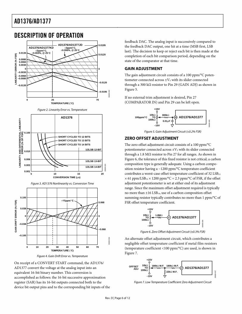
Figure 2. Linearity Error vs. Temperature
0.100
AD1376
0.001
0.003
0.006
0.010
5 10 15 2
0069
9-00
3
CONVERSION TIME (µs)
LIN
EAR
ITY
AN
D D
IFFE
REN
TIA
L LI
NEA
RIT
YER
RO
R (%
OF
FSR
)
0
SHORT CYCLED TO 12 BITS
1/2LSB 12-BIT
1/2LSB 13-BIT
1/2LSB 14-BIT
SHORT CYCLED TO 13 BITSSHORT CYCLED TO 14 BITS
Figure 3. AD1376 Nonlinearity vs. Conversion Time
0.100
0.038
–0.038
0
–0.068
0.068
0
–0.100
0 605040302010
0069
9-00
4
70
GA
IN D
RIF
T ER
RO
R (%
FSR
)
Figure 4. Gain Drift Error vs. Temperature
On receipt of a CONVERT START command, the AD1376/ AD1377 convert the voltage at the analog input into an equivalent 16-bit binary number. This conversion is accomplished as follows: the 16-bit successive approximation register (SAR) has its 16-bit outputs connected both to the device bit output pins and to the corresponding bit inputs of the
feedback DAC. The analog input is successively compared to the feedback DAC output, one hit at a time (MSB first, LSB last). The decision to keep or reject each bit is then made at the completion of each bit comparison period, depending on the state of the comparator at that time.
GAIN ADJUSTMENT The gain adjustment circuit consists of a 100 ppm/°C poten-tiometer connected across ±VS with its slider connected through a 300 kΩ resistor to Pin 29 (GAIN ADJ) as shown in Figure 5.
If no external trim adjustment is desired, Pin 27 (COMPARATOR IN) and Pin 29 can be left open.
0069
9-00
5
AD1376/AD137729
0.01µF
300kΩ
+15V
10kΩTO
100kΩ100ppm/°C
–15V
Figure 5. Gain Adjustment Circuit (±0.2% FSR)
ZERO OFFSET ADJUSTMENT The zero offset adjustment circuit consists of a 100 ppm/°C potentiometer connected across ±VS with its slider connected through a 1.8 MΩ resistor to Pin 27 for all ranges. As shown in Figure 6, the tolerance of this fixed resistor is not critical; a carbon composition type is generally adequate. Using a carbon compo-sition resistor having a −1200 ppm/°C temperature coefficient contributes a worst-case offset temperature coefficient of 32 LSB14 × 61 ppm/LSB14 × 1200 ppm/°C = 2.3 ppm/°C of FSR, if the offset adjustment potentiometer is set at either end of its adjustment range. Since the maximum offset adjustment required is typically no more than ±16 LSB14, use of a carbon composition offset summing resistor typically contributes no more than 1 ppm/°C of FSR offset temperature coefficient.
0069
9-00
6
AD1376/AD1377271.8MΩ
+15V
10kΩTO
100kΩ
–15V
Figure 6. Zero Offset Adjustment Circuit (±0.3% FSR)
An alternate offset adjustment circuit, which contributes a negligible offset temperature coefficient if metal film resistors (temperature coefficient <100 ppm/°C) are used, is shown in Figure 7.
0069
9-00
7
AD1376/AD137727
22kΩ M.F.
180kΩ M.F. 180kΩ M.F.
+15V
10kΩTO
100kΩOFFSET
ADJ
–15V
Figure 7. Low Temperature Coefficient Zero Adjustment Circuit
AD1376/AD1377
Rev. D | Page 7 of 12
In either adjustment circuit, the fixed resistor connected to Pin 27 should be located close to this pin to keep the pin connection short. Pin 27 is quite sensitive to external noise pickup and should be guarded by ANALOG COMMON.
TIMING The timing diagram is shown in Figure 8. Receipt of a CONVERT START signal sets the STATUS flag, indicating conversion in progress. This in turn removes the inhibit applied to the gated clock, permitting it to run through 17 cycles. All the SAR parallel bits, the STATUS flip-flops, and the gated clock inhibit signal are initialized on the trailing edge of the CONVERT START signal. At time t0, B1 is reset and B2–B16 are set unconditionally. At t1, the Bit 1 decision is made (keep) and Bit 2 is reset unconditionally. This sequence continues until the Bit 16 (LSB) decision (keep) is made at t16. The STATUS flag is reset, indicating that the conversion is complete and that the parallel output data is valid. Resetting the STATUS flag restores the gated clock inhibit signal, forcing the clock output to the low Logic 0 state. Note that the clock remains low until the next conversion.
Corresponding parallel data bits become valid on the same positive-going clock edge.
0069
9-00
8
t0 t1 t2 t3 t4 t5 t6 t7 t8 t9 t10 t11 t12 t13 t14 t15 t16
t17(3)(2)
(1)
0 1 1 0 0 1 1 1 0 1 1 1 1 0 1 0
0
1
10
0
11
10
1
1
11
0
10
MSB
STATUS
INTERNALCLOCK
CONVERTSTART
BIT 2BIT 3BIT 4BIT 5BIT 6BIT 7BIT 8BIT 9
BIT 10BIT 11BIT 12BIT 13BIT 14BIT 15
LSB LSBMSB
MAXIMUM THROUGHPUT TIME
CONVERSION TIME (2)
NOTES:1. THE CONVERT START PULSEWIDTH IS 50ns MIN AND MUST REMAIN LOW DURING A
CONVERSION. THE CONVERSION IS INITIATED BY THE TRAILING EDGE OF THECONVERT COMMAND.
2. MSB DECISION.3. CLOCK REMAINS LOW AFTER LAST BIT DECISION.
Figure 8. Timing Diagram (Binary Code 0110011101111010)
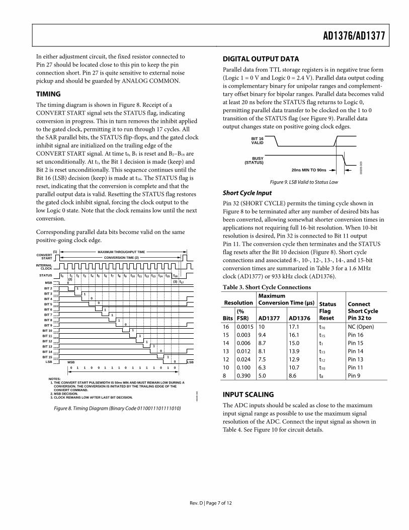
DIGITAL OUTPUT DATA Parallel data from TTL storage registers is in negative true form (Logic 1 = 0 V and Logic 0 = 2.4 V). Parallel data output coding is complementary binary for unipolar ranges and complement-tary offset binary for bipolar ranges. Parallel data becomes valid at least 20 ns before the STATUS flag returns to Logic 0, permitting parallel data transfer to be clocked on the 1 to 0 transition of the STATUS flag (see Figure 9). Parallel data output changes state on positive going clock edges.
0069
9-00
9
BIT 16VALID
BUSY(STATUS)
20ns MIN TO 90ns
Figure 9. LSB Valid to Status Low
Short Cycle Input
Pin 32 (SHORT CYCLE) permits the timing cycle shown in Figure 8 to be terminated after any number of desired bits has been converted, allowing somewhat shorter conversion times in applications not requiring full 16-bit resolution. When 10-bit resolution is desired, Pin 32 is connected to Bit 11 output Pin 11. The conversion cycle then terminates and the STATUS flag resets after the Bit 10 decision (Figure 8). Short cycle connections and associated 8-, 10-, 12-, 13-, 14-, and 15-bit conversion times are summarized in Table 3 for a 1.6 MHz clock (AD1377) or 933 kHz clock (AD1376).
Table 3. Short Cycle Connections
ResolutionMaximum Conversion Time (µs)
Bits(% FSR) AD1377 AD1376
Status Flag Reset
Connect Short Cycle Pin 32 to
16 0.0015 10 17.1 t16 NC (Open) 15 0.003 9.4 16.1 t15 Pin 16 14 0.006 8.7 15.0 t1 Pin 15 13 0.012 8.1 13.9 t13 Pin 14 12 0.024 7.5 12.9 t12 Pin 13 10 0.100 6.3 10.7 t10 Pin 11 8 0.390 5.0 8.6 t8 Pin 9
INPUT SCALING The ADC inputs should be scaled as close to the maximum input signal range as possible to use the maximum signal resolution of the ADC. Connect the input signal as shown in Table 4. See Figure 10 for circuit details.

AD1376/AD1377
Rev. D | Page 8 of 12
Table 4. Input Scaling Connections Input Signal Line Output Code Connect Pin 26 to Connect Pin 24 to Connect Input Signal to ±10 V COB Pin 271 Input Signal Pin 24 ±5 V COB Pin 271 Open Pin 25 ±2.5 V COB Pin 271 Pin 271 Pin 25 0 V to +5 V CSB Pin 22 Pin 271 Pin 25 0 V to +10 V CSB Pin 22 Open Pin 25 0 V to +20 V CSB Pin 22 Input Signal Pin 24 1 Pin 27 is extremely sensitive to noise and should be guarded by ANALOG COMMON.
0069
9-01
0
22ANALOGCOMMON
26BIPOLAROFFSET
COMP IN
24
25
27
7.5kΩ
R23.75kΩ
10V SPAN
20V SPAN R13.75kΩ
FROM DAC
COMPARATOR
TOSAR
VREF
Figure 10. Input Scaling Circuit
CALIBRATION (14-BIT RESOLUTION EXAMPLES) External zero adjustment and gain adjustment potentiometers, connected as shown in Figure 5 and Figure 6, are used for device calibration. To prevent interaction of these two adjustments, zero is always adjusted first and then gain. Zero is adjusted with the analog input near the most negative end of the analog range (0 for unipolar and minus full scale for bipolar input ranges). Gain is adjusted with the analog input near the most positive end of the analog range.
0 V to 10 V Range
Set analog input to +1 LSB14 = 0.00061 V. Adjust zero for digital output = 11111111111110. Zero is now calibrated. Set analog input to +FSR − 2 LSB = 9.99878 V. Adjust gain for 00000000000001 digital output code; full scale (gain) is now calibrated. Half-scale calibration check: set analog input to 5.00000 V; digital output code should be 01111111111111.
−10 V to +10 V Range
Set analog input to −9.99878 V; adjust zero for 1111111111110 digital output (complementary offset binary) code. Set analog input to 9.99756 V; adjust gain for 00000000000001 digital output (complementary offset binary) code. Half-scale calibration check: set analog input to 0.00000 V; digital output (complementary offset binary) code should be 01111111111111.
0069
9-01
1
–15V
+15V A
16-BIT SUCCESSIVEAPPROMIXATION REGISTER
16-BIT DACREFCONTROL
3.75
kΩ3.
75kΩ
24262319
29
28
22
21
25
eIN(0V TO +10V)
IIN
KEEP/REJECT
7.5kΩ
+15V
–15V
ZEROADJ
10kΩTO
100kΩ
27
IOS = 1.3mA
AD1376/AD1377
1.8MΩ1µF
+5V+
30
+1µF
+1µF
+15V
–15VGAINADJ
10kΩTO
100kΩ
300kΩ
0.01µF
NOTE:ANALOG ( ) AND DIGITAL ( ) GROUNDS ARE NOT TIED INTERNALLY AND MUST BE CONNECTED EXTERNALLY.
Figure 11. Analog and Power Connections for Unipolar 0 V to 10 V Input Range
0069
9-01
2
–15V
+15V A
16-BIT SUCCESSIVEAPPROMIXATION REGISTER
16-BIT DACREFCONTROL
3.75
kΩ3.
75kΩ
24262319
29
28
22
21
25
eIN(–10V TO +10V)
IIN
KEEP/REJECT
7.5kΩ
+15V
–15V
ZEROADJ
10kΩTO
100kΩ
27
IOS = 1.3mA
AD1376/AD1377
1.8MΩ1µF
+5V+
30
+1µF
+1µF
+15V
–15VGAINADJ
10kΩTO
100kΩ
300kΩ
0.01µF
NOTE:ANALOG ( ) AND DIGITAL ( ) GROUNDS ARE NOT TIED INTERNALLY AND MUST BE CONNECTED EXTERNALLY
Figure 12. Analog and Power Connections for Bipolar −10 V to +10 V Input Range
Other Ranges
Representative digital coding for 0 V to +10 V and −10 V to +10 V ranges is given in the 0 V to 10 V Range section and −10 V to +10 V Range section. Coding relationships and calibration points for 0 V to +5 V, −2.5 V to +2.5 V, and −5 V to +5 V ranges can be found by halving proportionally the corresponding code equivalents listed for the 0 V to +10 V and −10 V to +10 V ranges, respectively, as indicated in Table 5.

AD1376/AD1377
Rev. D | Page 9 of 12
Table 5. Transition Values vs. Calibration Codes Output Code MSB LSB1 Range ±10 V ±5 V ±2.5 V 0 V to +10 V 0 V to +5 V 000 ………0002 +Full Scale +10 V +5 V +2.5 V +10 V +5 V −3/2 LSB −3/2 LSB −3/2 LSB −3/2 LSB −3/2 LSB 011………111 Midscale 0 V 0 V 0 V +5 V +2.5 V –1/2 LSB –1/2 LSB –1/2 LSB –1/2 LSB –1/2 LSB 111………110 −Full Scale −10 V −5 V −2.5 V 0 V 0 V +1/2 LSB +1/2 LSB +1/2 LSB +1/2 LSB +1/2 LSB
1 For LSB value for range and resolution used, see Ta . ble 6
Table 6. Input Voltage Range and LSB Values
2 Voltages given are the nominal value for transition to the code specified.
Analog Input Voltage Range ±10 V ±5 V ±2.5 V 0 V to +10 V 0 V to +5 V Code Designation COB1 or CTC2 COB1 or CTC2 COB1 or CTC2 CSB3 CSB3
One Least Significant Bit (LSB) n2FSR
n2V20
n2V10
n2V5
n2V10
n2V5
n = 8 78.13 mV 39.06 mV 19.53 mV 39.06 mV 19.53 mV n = 10 19.53 mV 9.77 mV 4.88 mV 9.77 mV 4.88 mV n = 12 4.88 mV 2.44 mV 1.22 mV 2.44 mV 1.22 mV n = 13 2.44 mV 1.22 mV 0.61 mV 1.22 mV 0.61 mV n = 14 1.22 mV 0.61 mV 0.31 mV 0.61 mV 0.31 mV n = 15 0.61 mV 0.31 mV 0.15 mV 0.31 mV 0.15 mV
1 COB = complementary offset binary. 2 CTC = complementary twos complement—achieved by using an inverter to complement the most significant bit to produce MSB. 3 CSB = complementary straight binary
Zero- and full-scale calibration can be accomplished to a precision of approximately ±1/2 LSB using the static adjustment procedure described previously. By summing a small sine or triangular wave voltage with the signal applied to the analog input, the output can be cycled through each of the calibration codes of interest to more accurately determine the center (or end points) of each discrete quantization level. A detailed description of this dynamic calibration technique is presented in Analog-Digital Conversion Handbook, edited by D. H. Sheingold, Prentice Hall, Inc., 1986.
GROUNDING, DECOUPLING, AND LAYOUT CONSIDERATIONS Many data acquisition components have two or more ground pins that are not connected together within the device. These grounds are usually referred to as DIGITAL COMMON (logic power return), ANALOG COMMON (analog power return), or analog signal ground. These grounds (Pin 19 and Pin 22) must be tied together at one point as close as possible to the converter. Ideally, a single solid analog ground plane under the converter would be desirable. Current flows through the wires and etch stripes of the circuit cards, and since these paths have resistance and inductance, hundreds of millivolts can be generated between the system analog ground point and the ground pins of the ADC. Separate wide conductor stripe ground returns should be provided for high resolution converters to minimize noise and IR losses from the current
flow in the path from the converter to the system ground point. In this way, ADC supply currents and other digital logic-gate return currents are not summed into the same return path as analog signals where they would cause measurement errors.
Each of the ADC supply terminals should be capacitively decoupled as close to the ADC as possible. A large value (such as 1 µF) capacitor in parallel with a 0.1 µF capacitor is usually sufficient. Analog supplies are to be bypassed to the ANALOG COMMON (analog power return) Pin 22 and the logic supply is bypassed to DIGITAL COMMON (logic power return) Pin 19.
The metal cover is internally grounded with respect to the power supplies, grounds, and electrical signals. Do not externally ground the cover.
CLOCK RATE CONTROL The AD1376/AD1377 can be operated at faster conversion times by connecting the clock rate control (Pin 23) to an external multiturn trim potentiometer (TCR <100 ppm/°C) as shown in Figure 13.
0069
9-01
3
AD1376/AD1377232.25MHz @ 5V
1750kHz @ DGND
15V DC
5kΩ
Figure 13. Clock Rate Control Circuit

AD1376/AD1377
Rev. D | Page 10 of 12
HIGH RESOLUTION DATA ACQUISITION SYSTEM The essential details of a high resolution data acquisition system using a 16-bit sample-and-hold amplifier (SHA) and the AD1376/AD1377 are shown in Figure 14. Conversion is initiated by the falling edge of the CONVERT START pulse. This edge drives the device’s STATUS line high. The inverter then drives the SHA into hold mode. STATUS remains high throughout the conversion and returns low once the conversion is completed. This allows the SHA to re-enter track mode.
This circuit can exhibit nonlinearities arising from transients produced at the ADC’s input by the falling edge of CONVERT START. This edge resets the ADC’s internal DAC; the resulting transient depends on the SHA’s present output voltage and the ADC’s prior conversion result. In the circuit of Figure 15, the falling edge of CONVERT START also places the SHA into hold mode (via the ADC’s STATUS output), causing the reset transient to occur at the same moment as the SHA’s track-and-hold transition. Timing skews and capacitive coupling can cause some of the transient signal to add to the signal being acquired by the SHA, introducing nonlinearity.
0069
9-01
4
SHA AD1376/AD1377
30 21 28
22
242726
19
18 31
BITS1–16
+
CONVERTSTART
–10V TO +10V
+10µF +10µF
10µF
+15V–15V+5V
ANALOGINPUT
–10V TO +10V
Figure 14. Basic Data Acquisition System Interconnections 16-Bit SHA
A much safer approach is to add a flip-flop, as shown in Figure 15. The rising edge of CONVERT START places the track-and-hold device into hold mode before the ADC reset transients begin. The falling edge of STATUS places the SHA back into track mode. System throughput will be reduced if a long CONVERT START pulse is used. Throughput can be calculated from
CSCONVACQ TTTThroughput
++= 1
where:
TACQ is the track-and-hold acquisition time. TCONV is the time required for the ADC conversion. TCS is the duration of CONVERT START.
The combination of the AD1376 and a 16-bit SHA can provide greater than 50 kHz throughput. No significant track-and-hold droop error will be introduced, provided the width of CONVERT START is small compared with the ADC’s conversion time.
0069
9-01
5
SHAAD1376/AD1377
30 21 28
22
242726
1918 31
BITS1–16
+
–10V TO +10V
+10µF +10µF
10µF
+15V–15V+5V
ANALOGINPUT
–10V TO +10V
CONVERTSTART
HC112
S
R
QJ
QK
+5V
Figure 15. Improved Data Acquisition System
1

AD1376/AD1377
Rev. D | Page 11 of 12
APPLICATIONS The AD1376/AD1377 are excellent for use in high resolution applications requiring moderate speed and high accuracy or stability over commercial (0°C to 70°C) temperature ranges. Typical applications include medical and analytic instrumen-tation, precision measurement for industrial robotics, automatic test equipment (ATE), multichannel data acquisition systems, servo control systems, or anywhere wide dynamic range is required. A proprietary monolithic DAC and laser-trimmed thin-film resistors guarantee a maximum nonlinearity of ±0.003% (1/2 LSB14). The converters may be short cycled to achieve faster conversion times—15 µs to 14 bits for the AD1376 or 8 µs to 14 bits for the AD1377.
AD1376/AD1377
Rev. D | Page 12 of 12
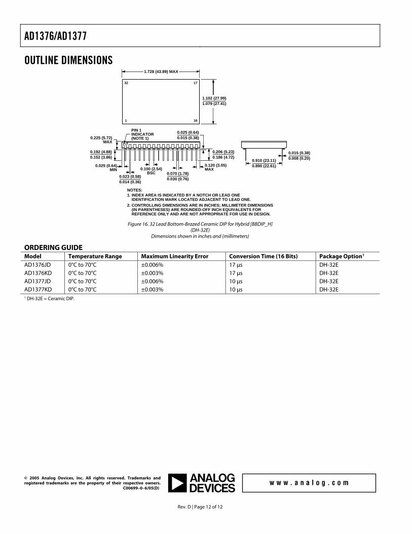
OUTLINE DIMENSIONS
NOTES:1. INDEX AREA IS INDICATED BY A NOTCH OR LEAD ONE IDENTIFICATION MARK LOCATED ADJACENT TO LEAD ONE.2. CONTROLLING DIMENSIONS ARE IN INCHES; MILLIMETER DIMENSIONS (IN PARENTHESES) ARE ROUNDED-OFF INCH EQUIVALENTS FOR REFERENCE ONLY AND ARE NOT APPROPRIATE FOR USE IN DESIGN.
0.023 (0.58)0.014 (0.36)
0.910 (23.11)0.890 (22.61)
1 16
1732
1.728 (43.89) MAX
0.225 (5.72)MAX
0.025 (0.64)0.015 (0.38)
0.015 (0.38)0.008 (0.20)
1.102 (27.99)1.079 (27.41)
0.100 (2.54)BSC 0.070 (1.78)
0.030 (0.76)
0.120 (3.05)MAX
PIN 1INDICATOR(NOTE 1)
0.192 (4.88)0.152 (3.86)
0.206 (5.23)0.186 (4.72)
0.025 (0.64)MIN
Figure 16. 32 Lead Bottom-Brazed Ceramic DIP for Hybrid [BBDIP_H] (DH-32E)
Dimensions shown in inches and (millimeters)
ORDERING GUIDE Model Temperature Range Maximum Linearity Error Conversion Time (16 Bits) Package Option1
AD1376JD 0°C to 70°C ±0.006% 17 µs DH-32E AD1376KD 0°C to 70°C ±0.003% 17 µs DH-32E AD1377JD 0°C to 70°C ±0.006% 10 µs DH-32E AD1377KD 0°C to 70°C ±0.003% 10 µs DH-32E
1 DH-32E = Ceramic DIP.
© 2005 Analog Devices, Inc. All rights reserved. Trademarks and registered trademarks are the property of their respective owners. C00699–0–6/05(D)