adc architectures - university of california,...
TRANSCRIPT
EECS 247 Lecture 21: Data Converters: Nyquist Rate ADCs © 2010 Page 1
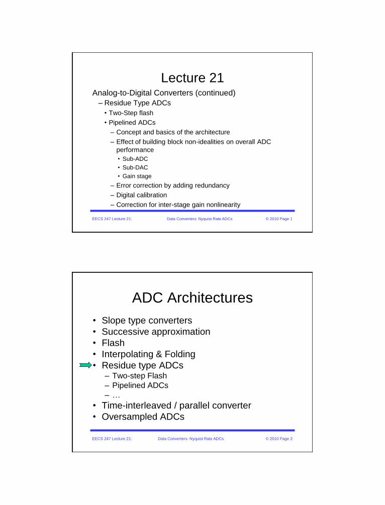
Lecture 21Analog-to-Digital Converters (continued)
– Residue Type ADCs
• Two-Step flash
• Pipelined ADCs
– Concept and basics of the architecture
– Effect of building block non-idealities on overall ADC
performance
• Sub-ADC
• Sub-DAC
• Gain stage
– Error correction by adding redundancy
– Digital calibration
– Correction for inter-stage gain nonlinearity
EECS 247 Lecture 21: Data Converters- Nyquist Rate ADCs © 2010 Page 2
ADC Architectures
• Slope type converters
• Successive approximation
• Flash
• Interpolating & Folding
• Residue type ADCs– Two-step Flash
– Pipelined ADCs
– …
• Time-interleaved / parallel converter
• Oversampled ADCs

EECS 247- Lecture 21 Residue Type ADCs © 2010 Page 3
Two-Step
Example: (2+2)Bits
• Using only one ADC: output contains large quantization error
• "Missing voltage" or "residue" ( -eq1)
• Idea: Use second ADC to quantize and add -eq1
0 1 2 3
00
01
10
11
0 1 2 3
-0.5
0.5
[LS
B]
ADC Input [LSB]
Vin
+
Dout = Vin + eq1
2-bit ADC 2-bit ADC
???
e q1
Dout
Vin
EECS 247- Lecture 21 Residue Type ADCs © 2010 Page 4
Two Stage Example
• Use DAC to compute missing voltage
• Add quantized representation of missing voltage
• Why does this help? How about eq2 ?
• Since maximum voltage at input of the 2nd ADC is Vref1/4 then for 2nd ADC Vref2=Vref1/4 and thus eq2= eq1/4 =Vref1/16 4bit overall resolution
Vin “Coarse“
+
Dout
= Vin
+ eq1
2-bit ADC 2-bit ADC
“Fine“+-
2-bit DAC
-eq1
-eq1+eq2
-eq1+eq2
Vref2Vref1

EECS 247- Lecture 21 Residue Type ADCs © 2010 Page 5
Two Step (2+2) Flash ADC
Vin Vin Vin
4-bit Straight Flash ADC Ideal 2-step Flash ADC
Voltage quantized
by 2nd ADC
EECS 247- Lecture 21 Residue Type ADCs © 2010 Page 6
Two Stage Example
• Fine ADC is re-used 22 times
• Fine ADC's full scale range needs to span only 1 LSB of coarse quantizer
22
1
2
2
2222
refref
q
VVe
00 01 10 11
Vref1
/22
-eq1
00
01
10
11
First ADC“Coarse“
Second ADC“Fine“VinVref1
Vref2

EECS 247- Lecture 21 Residue Type ADCs © 2010 Page 7
Two-Stage (2+2) ADC Transfer Function
0000
0001
0010
0011
0100
0101
01100111
1000
1001
1010
1011
1100
1101
11101111
Coarse
Bits
(MSB)
Fine
Bits
(LSB)
Dout
Vin
Vref1
EECS 247- Lecture 21 Residue Type ADCs © 2010 Page 8
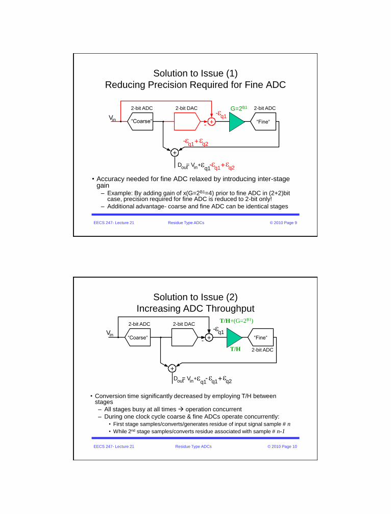
Residue or Multi-Step Type ADC
Issues
• Operation:– Coarse ADC determines MSBs
– DAC converts the coarse ADC output to analog- Residue is found by subtracting (Vin-VDAC)
– Fine ADC converts the residue and determines the LSBs
– Bits are combined in digital domain
• Issue:
1. Fine ADC has to have FS=FScoarse/2B1 & precision in the order of overall ADC
1/2LSB
2. Speed penalty Need at least 1 clock cycle per extra series stage to resolve one sample
(optional)Coarse ADC
(B1-Bit)
Vin
Residue
DAC(B1-Bit)
Fine ADC(B2-Bit)
Bit C
om
bin
er
(B1+
B2)-
Bit
EECS 247- Lecture 21 Residue Type ADCs © 2010 Page 9
Solution to Issue (1)
Reducing Precision Required for Fine ADC
• Accuracy needed for fine ADC relaxed by introducing inter-stage gain
– Example: By adding gain of x(G=2B1=4) prior to fine ADC in (2+2)bit case, precision required for fine ADC is reduced to 2-bit only!
– Additional advantage- coarse and fine ADC can be identical stages
Vin “Coarse“
+
Dout
= Vin
+ eq1
2-bit ADC 2-bit ADC
“Fine“+-
2-bit DAC-e
q1
-eq1+eq2
-eq1+eq2
G=2B1
EECS 247- Lecture 21 Residue Type ADCs © 2010 Page 10
Solution to Issue (2)
Increasing ADC Throughput
• Conversion time significantly decreased by employing T/H between stages
– All stages busy at all times operation concurrent
– During one clock cycle coarse & fine ADCs operate concurrently:
• First stage samples/converts/generates residue of input signal sample # n
• While 2nd stage samples/converts residue associated with sample # n-1
Vin“Coarse“
+
Dout
= Vin
+ eq1
2-bit ADC
2-bit ADC
“Fine“+-
2-bit DAC-e
q1
- eq1+eq2
T/H+(G=2B1)
T/H
EECS 247- Lecture 21 Pipelined ADCs © 2010 Page 11
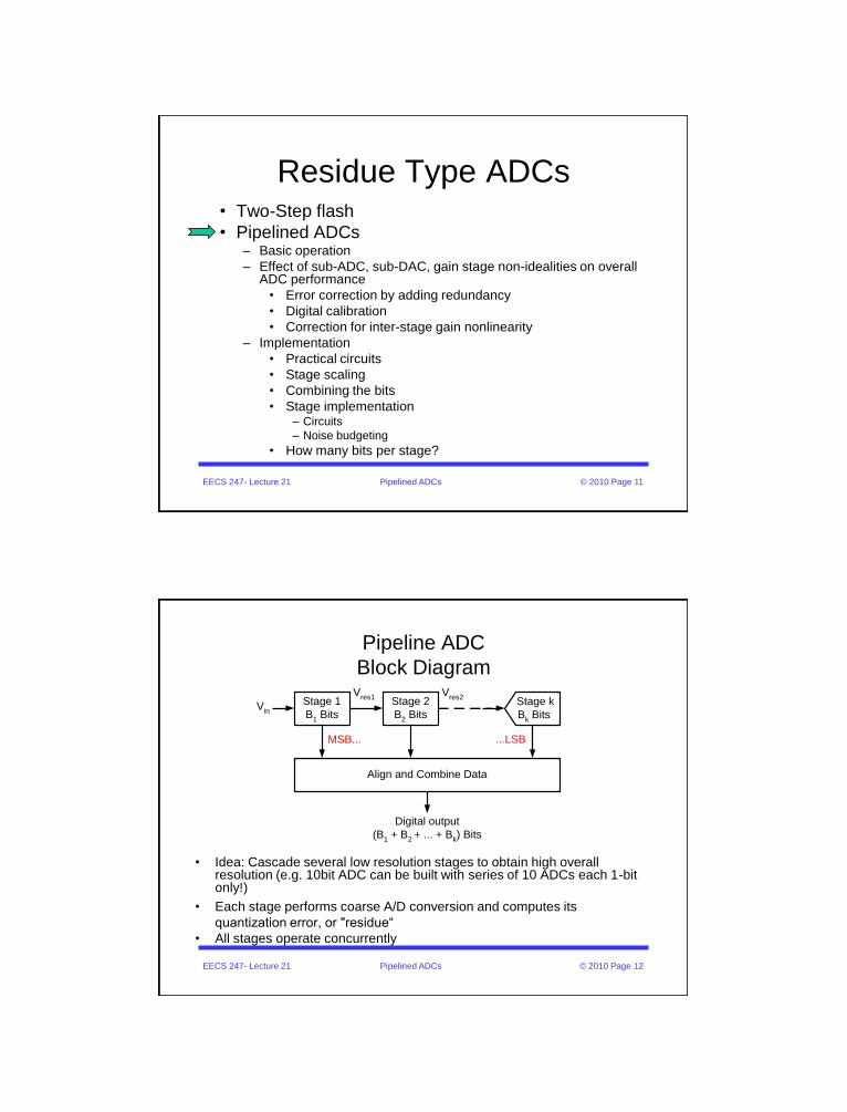
Residue Type ADCs• Two-Step flash
• Pipelined ADCs– Basic operation
– Effect of sub-ADC, sub-DAC, gain stage non-idealities on overall ADC performance
• Error correction by adding redundancy
• Digital calibration
• Correction for inter-stage gain nonlinearity
– Implementation
• Practical circuits
• Stage scaling
• Combining the bits
• Stage implementation– Circuits
– Noise budgeting
• How many bits per stage?
EECS 247- Lecture 21 Pipelined ADCs © 2010 Page 12
Pipeline ADC
Block Diagram
• Idea: Cascade several low resolution stages to obtain high overall resolution (e.g. 10bit ADC can be built with series of 10 ADCs each 1-bit only!)
• Each stage performs coarse A/D conversion and computes its
quantization error, or "residue“
• All stages operate concurrently
Align and Combine Data
Stage 1
B1 Bits
Stage 2
B2 Bits
Digital output
(B1 + B
2 + ... + B
k) Bits
Vin
MSB... ...LSB
Stage k
Bk Bits
Vres1
Vres2
EECS 247- Lecture 21 Pipelined ADCs © 2010 Page 13
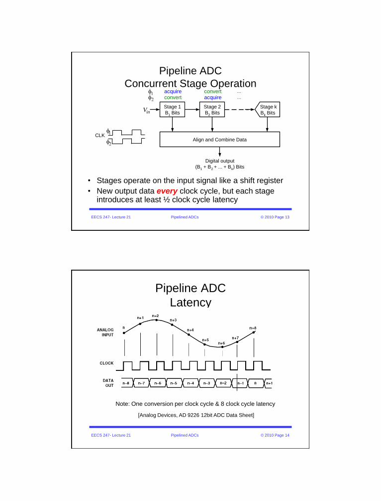
Pipeline ADC
Concurrent Stage Operation
• Stages operate on the input signal like a shift register
• New output data every clock cycle, but each stage introduces at least ½ clock cycle latency
Align and Combine Data
Stage 1
B1 Bits
Stage 2
B2 Bits
Digital output
(B1 + B2 + ... + Bk) Bits
VinStage k
Bk Bits
f1f2
acquireconvert
convertacquire
...
...
CLKf1
f2
EECS 247- Lecture 21 Pipelined ADCs © 2010 Page 14
Pipeline ADC
Latency
[Analog Devices, AD 9226 12bit ADC Data Sheet]
Note: One conversion per clock cycle & 8 clock cycle latency

EECS 247- Lecture 21 Pipelined ADCs © 2010 Page 15
Pipelined ADC
Characteristics
• Number of components (stages) grows linearly with resolution
• Pipelining– Trading latency for overall component count
– Latency may be an issue in e.g. control systems
– Throughput limited by speed of one stage Fast
• Versatile: 8...16bits, 1...400MS/s
• One important feature of pipelined ADCs: many analog circuit non-idealities can be corrected digitally
EECS 247- Lecture 21 Pipelined ADCs © 2010 Page 16
Pipeline ADC
Digital Data Alignment
• Digital shift register aligns sub-conversion
results in time
Stage 2
B2 BitsVin
Stage k
Bk Bits
f1f2
acquireconvert
convertacquire
...
...
+ +D
out
CLK CLK CLK
Stage 1
B1 Bits
CLKf1
f2

EECS 247- Lecture 21 Pipelined ADCs © 2010 Page 17
Cascading More Stages
• LSB of last stage becomes very small
• All stages need to have full precision
• Impractical to generate several Vref
VinADC
+-
DACADC
B3bitsB2bitsB1bits
Vref Vref /2B1 Vref /2
(B1+B2) Vref /2(B1+B2+B3)
EECS 247- Lecture 21 Pipelined ADCs © 2010 Page 18
Pipeline ADC
Inter-Stage Gain Elements
• Practical pipelines by adding inter-stage gain use single Vref
• Precision requirements decrease down the pipe
– Advantageous for noise, matching (later), power dissipation
• All stages can operate concurrently Throughput 1sample/clock cycle
VinADCB3bitsB2bitsB1bits
Vref
T/H&2B1
+-
DACADC
Vref Vref Vref
T/H&2B2T/H&2B3
EECS 247- Lecture 21 Pipelined ADCs © 2010 Page 19
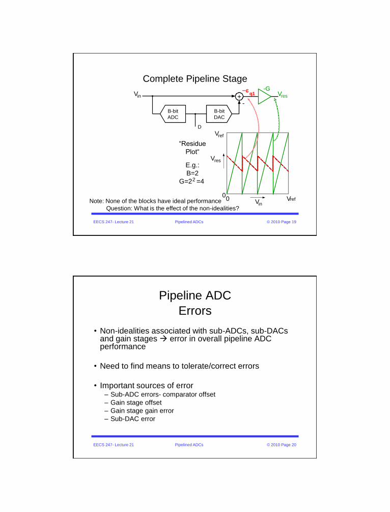
Complete Pipeline Stage
Vin +-
B-bit
DAC
B-bit
ADC
D
-GVres
Vin0
0
Vref
-eq1
“Residue
Plot“
E.g.:
B=2
G=22 =4
Vres
VrefNote: None of the blocks have ideal performance
Question: What is the effect of the non-idealities?
EECS 247- Lecture 21 Pipelined ADCs © 2010 Page 20
Pipeline ADC
Errors
• Non-idealities associated with sub-ADCs, sub-DACs and gain stages error in overall pipeline ADC performance
• Need to find means to tolerate/correct errors
• Important sources of error– Sub-ADC errors- comparator offset
– Gain stage offset
– Gain stage gain error
– Sub-DAC error

EECS 247- Lecture 21 Pipelined ADCs © 2010 Page 21
Pipeline ADC Single Stage
Model
Vin
-
Dout
-GV res
-eq
S
eq
S
Vres = Gxeq
EECS 247- Lecture 21 Pipelined ADCs © 2010 Page 22
Pipeline ADC Multi-Stage Model
1 q2 2
out in,ADC q1
d1 d1 d 2
q( n 1) ( n 1) qn
n 2 n 1
d( n 1)dj dj
j 1 j 1
G GD V 1 1
G G G
G.. . 1
GG G
ee
e e- -
- -
-
- -
-
S
Se
q1
- G1
S
S
Se
q2
- G2
S
S
Se
q(n-1)
- Gn-1
S
Vin,ADC
Dout 1/G
d11/G
d2
Vres1
Vres2
Vres(n-1)
S
1/Gd(n-1)
eqnD
1D
2D
(n-1)D
n

EECS 247- Lecture 21 Pipelined ADCs © 2010 Page 23
Pipeline ADC Model• If the "Analog" and "Digital" gain/loss is precisely matched:
-
-
-
-
1
1
2
1
1
2
1
1
1
1
log
2log
22
3log20
212
22log20
.log20..
n
j
jnADC
n
j
j
B
ADC
n
j
j
B
n
j
j
B
ref
ref
GBB
GB
G
G
V
V
NoiseQuantrms
SignalFSrmsRD
n
n
n
stage finalin bits of # & 2
where1
1
,
-
BnV
G
VDBn
ref
qnn
j
j
qn
ADCinout ee
EECS 247- Lecture 21 Pipelined ADCs © 2010 Page 24
Pipeline ADC
Observations
• The aggregate ADC resolution is independent of sub-ADC resolution!
• Effective stage resolution Bj=log2(Gj)
• Overall conversion error does not (directly)depend on sub-ADC errors!
• Only error term in Dout contains quantization error associated with the last stage
• So why do we care about sub-ADC errors?
Go back to two stage example
EECS 247- Lecture 21 Pipelined ADCs © 2010 Page 25
Pipeline ADC
Sub-ADC Errors
-
1
1
, n
j
j
qn
ADCinout
G
VDe
1
2
,G
VDq
ADCinout
e
Vin,ADC
ADC
2-bitsB1 =2-bits
Vref Vref
Vres1
Veq2Vin
00
Vref
Vres1
refVin Dout=1000
00 01 10 11
00
01
1
0
11
EECS 247- Lecture 21 Pipelined ADCs © 2010 Page 26
Pipeline ADC
Sub-ADC Errors
-
1
1
, n
j
j
qn
ADCinout
G
VDe
1
2
,G
VDq
ADCinout
e
Grows outside ½ LSB bounds
Vin,ADC
ADC
2-bitsB1 =2-bits
Vref Vref
Vres1
Veq2Vin
00
Vref
Vres1
ref
Voffset

EECS 247- Lecture 21 Pipelined ADCs © 2010 Page 27
Pipeline ADC1st-Stage Comparator Offset
First stage ADC Levels:
(Levels normalized to LSB)
Ideal comparator threshold: -1, 0, +1
Comparator threshold including offset: -1, 0.3, +1
Problem: Vres1 exceeds 2nd pipeline stage
overload range
Missing Code!
Overall ADC Transfer Curve
Vres1
Vres2
EECS 247- Lecture 21 Pipelined ADCs © 2010 Page 28
Pipeline ADC
Three Ways to Deal with Sub-ADC Errors
• All involve “sub-ADC redundancy”
• Redundancy in stage that produces errors
– Choose gain for residue to be processed by the 2nd stage < 2B1
– Higher resolution sub-ADC & sub-DAC
• Redundancy in succeeding stage(s)

EECS 247- Lecture 21 Pipelined ADCs © 2010 Page 29
(1) Inter-Stage Gain Following 1st Stage <2B1
00
VinADCB1 bits
Vref
eq2
Vres1
• Choose G1 less than
2B1
• Effective stage
resolution could
become non-integer
B1eff=log2G1
• E.g. if G1=3.8
B1eff=1.8bit
-Ref: A. Karanicolas et. al.,
JSSC 12/1993
Vref
Vref
Vres1
Vin
Vref
EECS 247- Lecture 21 Pipelined ADCs © 2010 Page 30
Correction Through Redundancy
“enlarged” residuum still within
input range of next stage
Overall ADC Transfer Curve
Vres1
Vres2
If G1=2 instead of 4
Only 1-bit resolution from first stage (3-bit
total) In spite of comparator offset: No overall
error!

EECS 247- Lecture 21 Pipelined ADCs © 2010 Page 31
(2) Higher Resolution Sub-ADC
VinADCB1 bits
Vref
Vres1
Vref
00
eq2
Vref
Vres1
Vin
Vref
• Keep G1 precise
power of two
(e.g. G1=4)
• Add extra decision
levels in sub-ADC
(e.g. add 1 extra bit to
1st stage)
• E.g. B1=B1eff+1
-Ref: Singer et. al., VSLI 1996
EECS 247- Lecture 21 Pipelined ADCs © 2010 Page 32
(3) Over-Range Accommodation
Through Increase in Following Stage Resolution
• No redundancy in
stage with errors
• Add extra decision
levels in succeeding
stage
Ref: Opris et. al.,
JSSC 12/1998V
in
Vref
00
Vref
Vres1
Vin,ADC
ADCB1 bits
Vref
Vref
eq2
Vres1

EECS 247- Lecture 21 Pipelined ADCs © 2010 Page 33
Redundancy• The preceding analysis applies to any stage
in an n-stage pipeline
• Can always perceive a multi-stage pipelined
ADC as a single stage + backend ADC
Vin
B4 bitsB
3 bitsB
2 bitsB
1 bits
Vin
B2+B
3+B
4 bitsB
1 bits
Vres1
EECS 247- Lecture 21 Pipelined ADCs © 2010 Page 34
Redundancy• In literature, sub-ADC redundancy schemes are often called "digital correction" – a misnomer!
• No error correction takes place
• We can tolerate sub-ADC errors as long as:–The residues stay "within the box", or
–Another stage downstream "returns the residue to “within the box" before it reaches last quantizer
• Let's calculate tolerable errors for popular "1.5 bits/stage" topology

EECS 247- Lecture 21 Pipelined ADCs © 2010 Page 35
1.5-Bit/Stage Pipelined ADC
Vres1
Vin +-
1.5-bit
DAC
1.5-bit
ADC
G=-2-eq1
• G=-2
• Effective bit/stage Beff=log2|G|=log22=1
• Actual bit/stage B=log2(2+1)=1.589...
• 1bit/stage + 0.5bit redundancy
Ref: Lewis et. al., JSSC 3/1992
EECS 247- Lecture 21 Pipelined ADCs © 2010 Page 36
1.5 Bits/Stage Example
• Comparators threshold levels placed strategically
• G=2
• Beff=log2G=log22=1
• B=log2(2+1)=1.589...
• 0.5bit redundancy
Ref: Lewis et. al., JSSC 3/1992
Vos=Vref/8
00
Vref
Vres1
Vin
Vref

EECS 247- Lecture 21 Pipelined ADCs © 2010 Page 37
3-Stage 1.5-bit-per-Stage Pipelined ADC
• All three stages
Comparator
with offset
• Overall transfer
curve
No missing
codes
Some DNL
error
Ref: S. Lewis et al, “A
10-b 20-MS/s
Analog-to-Digital
Converter,” J.
Solid-State Circ.,
pp. 351-8, March
1992
Overall Transfer Curve
Vres1
Vres2
Vres3
EECS 247- Lecture 21 Pipelined ADCs © 2010 Page 38
Summary So Far
Pipelined A/D Converters
Vin
ADC2B1eff 2B2 2B3
+-DACADC
B2
bitsB1
bits
• Cascade of low resolution stages
– Stages operate concurrently- trades latency for overall component count
– Throughput limited by speed of one stage Fast
• Errors and correction
– Built-in redundancy compensate for sub-ADC inaccuracies (interstage gain:
G=2Bneff, Bneff < Bn)
B3
bits2B2eff 2B3eff
VrefVref Vref Vref

EECS 247- Lecture 21 Pipelined ADCs © 2010 Page 39
Pipeline ADC
Errors
• Non-idealities associated with sub-ADCs, sub-DACs and gain stages error in overall pipeline ADC performance
• Need to find means to tolerate/correct errors
• Important sources of error– Sub-ADC errors- comparator offset
– Gain stage offset
– Gain stage error
– Sub-DAC error
EECS 247- Lecture 21 Pipelined ADCs © 2010 Page 40
Inter-Stage Amplifier Offset
• Input referred converter offset – usually no problem
• Equivalent sub-ADC offset - accommodated through
adequate redundancy
ADC DAC
-
D
Vres
Vin
G
Vos
-Vos
Vos

EECS 247- Lecture 21 Pipelined ADCs © 2010 Page 41
Pipeline ADC
Errors
• Non-idealities associated with sub-ADCs, sub-DACs and gain stages error in overall pipeline ADC performance
• Need to find means to tolerate/correct errors
• Important sources of error– Sub-ADC errors- comparator offset
– Gain stage offset
– Gain stage gain error
– Sub-DAC error
EECS 247- Lecture 21 Pipelined ADCs © 2010 Page 42
Gain Stage Gain Error
1, 1
1
2 ( 1) ( 1)2
2 11 2 ( 1)
1 1
1
1 ... 1
out in ADC qd
q q n n qn
n nd d d n
dj dj
j j
GD V
G
GG
G G GG G
e
e e
e- -
- --
-
- -
S
S
eq1
-
S
S
S
eq2
- G2
S
S
S
eq(n-1)
- Gn-1
S
Vin,ADC
Dout 1/(G
d1+ ) 1/G
d2
Vres1
Vres2
Vres(n-1)
S
1/Gd(n-1)
eqnD
1D
2D
(n-1)D
n
- Resolution is function of log2G therefore error in G affects resolution
Small amount of gain error can be tolerated

EECS 247- Lecture 21 Pipelined ADCs © 2010 Page 43
Interstage Gain Error
-1 -0.5 0 0.5 11
0
1First Stage Residue (Gain Error)
Vin
Vre
s
1 0.5 0 0.5 11
0
1Converter Transfer Function (Gain Error)
Vin
Dou
t
1 0.5 0 0.5 10.2
0
0.2Transfer Function Error(Gain Error)
Vin
Dou
t(id
eal)
-D
ou
t
EECS 247- Lecture 21 Pipelined ADCs © 2010 Page 44
Gain Stage Gain Inaccuracy
• Gain error can be compensated in
digital domain – "Digital Calibration"
• Problem: Need to measure/calibrate
digital correction coefficient
• Example: Calibrate 1-bit first stage
• Objective: Measure G in digital domain

EECS 247- Lecture 21 Pipelined ADCs © 2010 Page 45
ADC ModelV
in +-
1-bit
DAC
1-bit
ADC
D
GV
res1
Vin
Vref
00
Vref
Vres1
D=0 D=1
BackendD
back
DACinres VVGV -1
2/)1(
0)0(
refDAC
DAC
VDV
DV
2
Vref
G Vin
-
inG V
EECS 247- Lecture 21 Pipelined ADCs © 2010 Page 46
Gain Stage Inacurracy
Calibration – Step 1
Vin= const.
+-
1-bit
DAC
1-bit
ADCD
G
Vres1
(1)
Backend
Dback
(1)
M
U
X
“1“
Vref
storeV
VVGD
VVGV
ref
refin
back
refinres
-
-
2/
2/
)1(
)1(
1

EECS 247- Lecture 21 Pipelined ADCs © 2010 Page 47
Gain Stage Inacurracy
Calibration – Step 2
Vin= const.
+-
1-bit
DAC
1-bit
ADCD
G
Vres1
(2)
Backend
Dback
(2)
M
U
X
“0“
Vref
store
V
VGD
VGV
ref
inback
inres
-
-
0
0
)2(
)2(
1
EECS 247- Lecture 21 Pipelined ADCs © 2010 Page 48
Gain Stage Inacurracy
Calibration – Evaluate
GDD
V
VGD
V
VVGD
backback
ref
inback
ref
refin
back
-
-----------------
--
-
2
1
0
2/
)2()1(
)2(
)1(
• To minimize the effect of backend ADC noise perform measurement several times and take the average
EECS 247- Lecture 21 Pipelined ADCs © 2010 Page 49
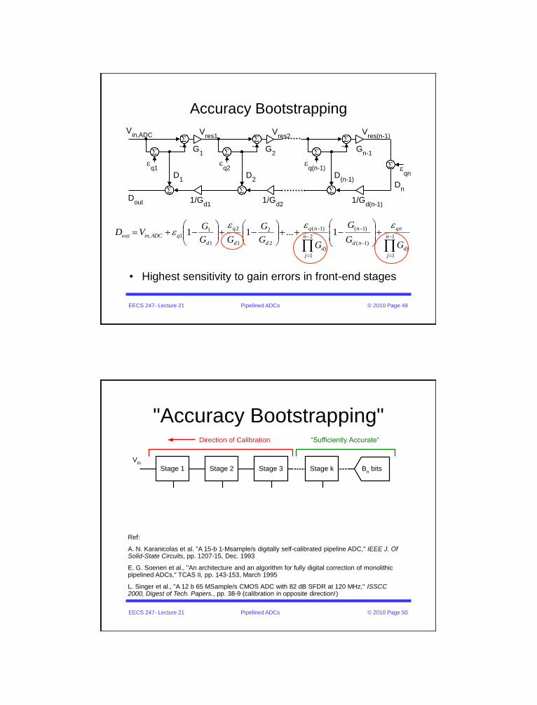
Accuracy Bootstrapping
• Highest sensitivity to gain errors in front-end stages
-
-
-
-
-
-
-
-
1
1
)1(
)1(
2
1
)1(
2
2
1
2
1
11, 1...11
n
j
dj
qn
nd
n
n
j
dj
nq
dd
q
d
qADCinout
GG
G
GG
G
GG
GVD
eeee
S
S
eq1
- G1
S
S
S
eq2
- G2
S
S
S
eq(n-1)
- Gn-1
S
Vin,ADC
Dout 1/G
d11/G
d2
Vres1
Vres2
Vres(n-1)
S
1/Gd(n-1)
eqnD
1D
2D
(n-1)D
n
EECS 247- Lecture 21 Pipelined ADCs © 2010 Page 50
"Accuracy Bootstrapping"
Vin
Bn bitsStage 3Stage 2Stage 1 Stage k
“Sufficiently Accurate“Direction of Calibration
Ref:
A. N. Karanicolas et al. "A 15-b 1-Msample/s digitally self-calibrated pipeline ADC," IEEE J. Of Solid-State Circuits, pp. 1207-15, Dec. 1993
E. G. Soenen et al., "An architecture and an algorithm for fully digital correction of monolithic pipelined ADCs," TCAS II, pp. 143-153, March 1995
L. Singer et al., "A 12 b 65 MSample/s CMOS ADC with 82 dB SFDR at 120 MHz," ISSCC 2000, Digest of Tech. Papers., pp. 38-9 (calibration in opposite direction!)

EECS 247- Lecture 21 Pipelined ADCs © 2010 Page 51
Pipeline ADC
Errors
• Non-idealities associated with sub-ADCs, sub-DACs and gain stages error in overall pipeline ADC performance
• Need to find means to tolerate/correct errors
• Important sources of error– Sub-ADC errors- comparator offset
– Gain stage offset
– Gain stage error
– Sub-DAC error
EECS 247- Lecture 21 Pipelined ADCs © 2010 Page 52
DAC Errors
• Can be corrected digitally as well
• Same calibration concept as gain errors Vary DAC codes & measure errors via backend ADC
Vin +-
B1-bit
DAC
D
GV
res1
Dback
B1-bit
ADC+
Dout
- 1/G
eDAC
+
Backend
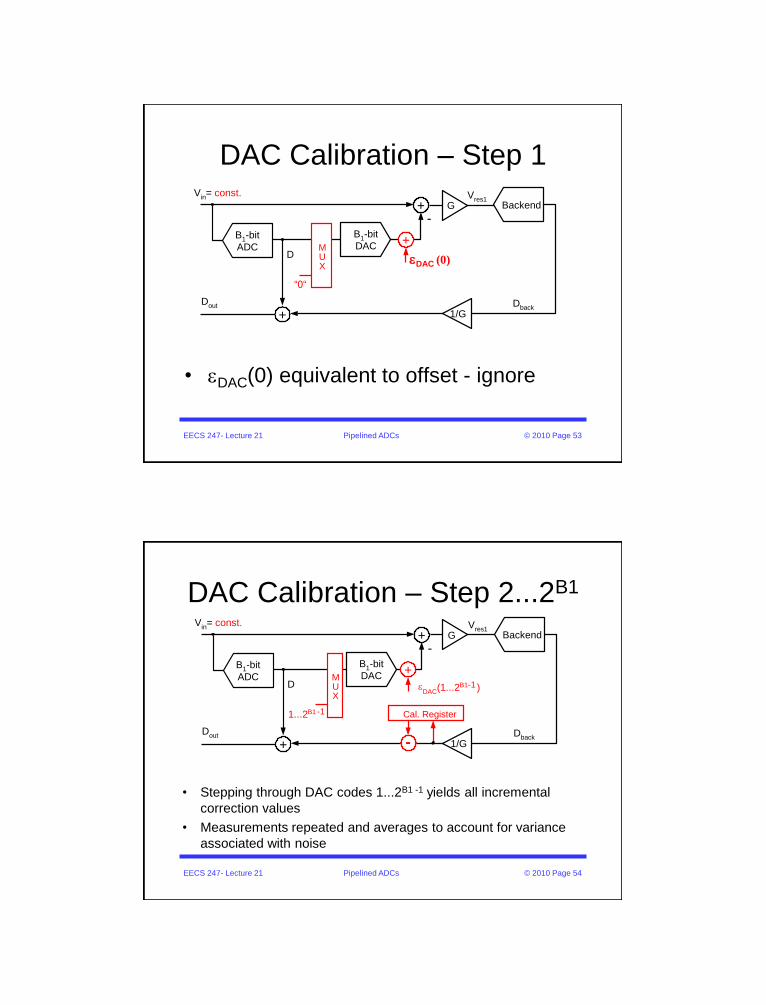
EECS 247- Lecture 21 Pipelined ADCs © 2010 Page 53
DAC Calibration – Step 1
• eDAC(0) equivalent to offset - ignore
+-
B1-bit
DACD
GVres1
Dback
B1-bit
ADC+
Dout
1/G
Backend
Vin= const.
MUX
“0“
+
eDAC (0)
EECS 247- Lecture 21 Pipelined ADCs © 2010 Page 54
DAC Calibration – Step 2...2B1
• Stepping through DAC codes 1...2B1 -1 yields all incremental
correction values
• Measurements repeated and averages to account for variance
associated with noise
+-
B1-bit
DACD
GVres1
Dback
B1-bit
ADC+
Dout
1/G
eDAC(1...2B1-1 )
Backend
Vin= const.
MUX
1...2B1 -1
+
Cal. Register
-

EECS 247- Lecture 21 Pipelined ADCs © 2010 Page 55
Pipeline ADC
Example: Calibration Hardware
• Above block diagram may seem extensive however, in current fine-line CMOS technologies digital portion of a pipeline ADCs consume insignificant power and area compared to the analog sections
Ref: E. G. Soenen et al., "An architecture and an algorithm for fully digital correction of monolithic pipelined ADCs," TCAS II, pp. 143-153, March 1995
EECS 247- Lecture 21 Pipelined ADCs © 2010 Page 56
Summary So Far
Pipelined A/D Converters
Vin
ADC2B1eff 2B2 2B3B2
bitsB1
bits
• Cascade of low resolution stages
– By adding inter-stage gain= 2Beff
• No need to scale down Vref for stages down the pipe
• Reduced accuracy requirement for stages coming after stage 1
– Addition of Track & Hold function to interstage-gain
• Stages can operate concurrently
• Throughput increased to as high as one sample per clock cycle
• Latency function of number of stages & conversion-per-stage
– Correction for circuit non-idealities
• Built-in redundancy compensate for sub-ADC inaccuracies such as comparator
offset (interstage gain: G=2Bneff, Bneff < Bn)
• Error associated with gain stage and sub-DAC calibrated out
B3
bits2B2eff 2B3eff
VrefVref Vref Vref
T/H+Gain