ads1148evm, ads1248evm, ads1148evm-pdk,and ... - ti.com · • easily expandable with new analysis...
TRANSCRIPT

User's GuideSBAU142B–April 2009–Revised May 2011
ADS1148EVM, ADS1248EVM, ADS1148EVM-PDK, andADS1248EVM-PDK
ADS1248EVM (Left) and ADS1248EVM-PDK (Right)
This user's guide describes the characteristics, operation, and use of the ADS1148EVM andADS1248EVM, both by themselves and as part of the ADS1148EVM-PDK or ADS1248EVM-PDK. Theseevaluation modules (EVMs) are evaluation boards for the ADS1248, a 24-bit, multi-channel, delta-sigmaanalog-to-digital converter (ADC), and the ADS1148, a 16-bit version of the ADS1248. This EVM allowsevaluation of all aspects of the ADS1148 or ADS1248 devices. Complete circuit descriptions, schematicdiagrams, and bills of material are included in this document.
The following related documents are available for download through the Texas Instruments web site athttp://www.ti.com.
EVM-Compatible Device Data Sheets
Device Literature Number
ADS1148 SBAS453
ADS1248 SBAS426A
REF5020 SBOS410D
OPA227 SBOS110A
TPS3836L30 SLVS292D
TPS79225 SLVS337B
TPS72325 SLVS346B
SN74LVC2G157 SCES207K
PCA9535 SCPS129I
ADCPro is a trademark of Texas Instruments.Microsoft, Windows are registered trademarks of Microsoft Corporation.I2C is a trademark of NXP Semiconductors.All other trademarks are the property of their respective owners.
1SBAU142B–April 2009–Revised May 2011 ADS1148EVM, ADS1248EVM, ADS1148EVM-PDK, and ADS1248EVM-PDKSubmit Documentation Feedback
Copyright © 2009–2011, Texas Instruments Incorporated

www.ti.com
Contents1 EVM Overview ............................................................................................................... 32 Analog Interface ............................................................................................................. 33 Digital Interface .............................................................................................................. 44 Power Supplies .............................................................................................................. 55 Voltage Reference .......................................................................................................... 66 Clock Source ................................................................................................................ 67 EVM Operation .............................................................................................................. 78 ADS1248EVM-PDK Kit Operation ........................................................................................ 89 Evaluating Performance with the ADCPro Software .................................................................. 1710 Schematics and Layout ................................................................................................... 29
List of Figures
1 Reference Select Switch S1 ............................................................................................... 6
2 Jumper J2.................................................................................................................... 7
3 ADS1248EVM Default Jumper Locations................................................................................ 8
4 Virtual COM Port Installer.................................................................................................. 9
5 Virtual COM Port Setup .................................................................................................... 9
6 MMB3 Switch Locations .................................................................................................. 10
7 Connecting ADS1248EVM to MMB3 ................................................................................... 11
8 MMB3 Block Diagram..................................................................................................... 12
9 ADCPro Software Start-up Display Window ........................................................................... 13
10 ADS1248EVM-PDK Plug-In Display Window.......................................................................... 14
11 Connection Timeout....................................................................................................... 15
12 Firmware Download Message Box...................................................................................... 15
13 Firmware Download Progress Indicator ................................................................................ 16
14 Firmware Download Complete Message Box ......................................................................... 17
15 ADS1248 Multiplexer...................................................................................................... 18
16 I/O Config Tab ............................................................................................................. 19
17 Enabling VBIAS on a Channel........................................................................................... 20
18 GPIO Tab................................................................................................................... 21
19 GPIO Set to Output Mode ................................................................................................ 22
20 GPIO Output Set to High ................................................................................................. 23
21 Power & Ref Tab .......................................................................................................... 24
22 Cal Tab ..................................................................................................................... 26
23 About Tab .................................................................................................................. 27
24 Progress Bar While Collecting Data .................................................................................... 28
List of Tables
1 J8/J4: Analog Interface Pinout ............................................................................................ 4
2 J7: Serial Interface Pins.................................................................................................... 4
3 J11 Configuration: Power-Supply Input .................................................................................. 5
4 J10 Configuration: Power Options ........................................................................................ 5
5 REF1 Reference Voltage Options ........................................................................................ 6
6 List of Switches.............................................................................................................. 8
7 ADS1148EVM/ADS1248EVM Bill of Materials ....................................................................... 29
2 ADS1148EVM, ADS1248EVM, ADS1148EVM-PDK, and ADS1248EVM-PDK SBAU142B–April 2009–Revised May 2011Submit Documentation Feedback
Copyright © 2009–2011, Texas Instruments Incorporated

www.ti.com EVM Overview
1 EVM Overview
1.1 Features
ADS1148EVM/ADS1248EVM Features:• Contains all support circuitry needed for the ADS1148/ADS1248• ±2.5V and +5V power-supply options for ADC• Voltage reference options: external or onboard• GPIO access• Compatible with the TI Modular EVM System
ADS1148EVM-PDK/ADS1248EVM-PDK Features:• Easy-to-use evaluation software for Microsoft® Windows® XP• Data collection to text files• Built-in analysis tools including scope, FFT, and histogram displays• Complete control of board settings• Easily expandable with new analysis plug-in tools from Texas Instruments
For use with a computer, the ADS1148EVM-PDK or ADS1248EVM-PDK is available. This kit combinesthe ADS1148/ADS1248EVM board with the MSP430-based MMB3 motherboard, and includes ADCPro™software for evaluation.
The MMB3 motherboard allows the ADS1148/ADS1248EVM to be connected to the computer via anavailable USB port. This manual shows how to use the MMB3 as part of theADS1148EVM-PDK/ADS1248EVM-PDK, but does not provide technical details about the MMB3 itself.
ADCPro is a program for collecting, recording, and analyzing data from ADC evaluation boards. It is basedon a number of plug-in programs, so it can be expanded easily with new test and data collection plug-ins.The ADS1148EVM-PDK/ADS1248EVM-PDK is controlled by a plug-in that runs in ADCPro. For moreinformation about ADCPro, see the ADCPro™ Analog-to-Digital Converter Evaluation Software User'sGuide (literature number SBAU128), available for download from the TI web site.
This manual covers the operation of both the ADS1148/ADS1248EVM and theADS1148EVM-PDK/ADS1248EVM-PDK. Throughout this document, the abbreviation EVM and the termevaluation module are synonymous with the ADS1148/ADS1248EVM. For clarity of reading, the remainderof this manual will refer only to the ADS1248EVM or ADS1248EVM-PDK, but operation of the EVM and kitfor the ADS1148 is identical, unless otherwise noted.
1.2 Introduction
The ADS1248EVM is an evaluation module built to the TI Modular EVM System specification. It can beconnected to any modular EVM system interface card.
The ADS1248EVM is available as a stand-alone printed circuit board (PCB) or as part of theADS1248EVM-PDK, which includes an MMB3 motherboard and software. As a stand-alone PCB, theADS1248EVM is useful for prototyping designs and firmware.
Note that the ADS1248EVM has no microprocessor and cannot run software. To connect it to a computer,some type of interface is required.
2 Analog Interface
For maximum flexibility, the ADS1248EVM is designed for easy interfacing to multiple analog sources.Samtec part numbers SSW-110-22-F-D-VS-K and TSM-110-01-T-DV-P provide a convenient 10-pin,dual-row, header/socket combination at J8. This header/socket provides access to the analog input pins ofthe ADS1248. Consult Samtec at http://www.samtec.com or call 1-800-SAMTEC-9 for a variety of matingconnector options. These signals can also be connected to the terminal block J4.
3SBAU142B–April 2009–Revised May 2011 ADS1148EVM, ADS1248EVM, ADS1148EVM-PDK, and ADS1248EVM-PDKSubmit Documentation Feedback
Copyright © 2009–2011, Texas Instruments Incorporated

Digital Interface www.ti.com
All of the pins on J4 and J8 are connected with minimal filtering or protection. Use appropriate cautionwhen handling these pins. Table 1 summarizes the pinouts for analog interfaces J4 and J8.
Table 1. J8/J4: Analog Interface Pinout
Pin Number Signal Description, ADS1148/ADS1248
J8.1, J4-1 A0(–) AIN0
J8.2, J4-2 A0(+) AIN1
J8.3, J4-3 A1(–) AIN2
J8.4, J4-4 A1(+) AIN3
J8.5, J4-5 A2(–) AIN4
J8.6, J4-6 A2(+) AIN5
J8.7, J4-7 A3(–) AIN6
J8.8, J4-8 A3(+) AIN7
J8.18 REF– External reference source input (–side of differential input)
J8.20 REF+ External reference source input (+side of differential input)
J8.10-16 (even) Unused
J8.15 Unused
J8.9-19 (odd), J4-9 AGND Analog ground connections(except J8.15)
3 Digital Interface
3.1 Serial Data Interface
The ADS1248EVM is designed to easily interface with multiple control platforms. Samtec part numbersSSW-110-22-F-D-VS-K and TSM-110-01-T-DV-P provide a convenient 10-pin, dual-row, header/socketcombination at J7. This header/socket provides access to the digital control and serial data pins of theADC. Consult Samtec at http://www.samtec.com or call 1-800-SAMTEC-9 for a variety of matingconnector options.
All logic levels on J7 are 3.3V CMOS, except for the I2C™ pins. These pins conform to 3.3V I2C rules.Table 2 describes the J7 serial interface pins.
Table 2. J7: Serial Interface Pins
Pin No. Pin Name Signal Name I/O Type Pullup Function
J7.1 CNTL CS In High
J7.2 GPIO0 START In High
J7.3 CLKX SCLK In None ADS1248 SPI clock
J7.4 DGND DGND In/Out None Digital ground
J7.5 CLKR Unused – –J7.6 GPIO1 MR In High Master reset
J7.7 FSX Unused – –J7.8 GPIO2 Unused – –J7.9 FSR DRDY Out None
J7.10 DGND DGND In/Out None Digital ground
J7.11 DX DIN In None ADS1248 SPI data in
J7.12 GPIO3 PWRSEL In High Selects ±2.5V or +5Vsupply
J7.13 DR DOUT/DRDY Out None ADS1248 data out
J7.14 GPIO4 Unused – –J7.15 INT DRDY Out None
4 ADS1148EVM, ADS1248EVM, ADS1148EVM-PDK, and ADS1248EVM-PDK SBAU142B–April 2009–Revised May 2011Submit Documentation Feedback
Copyright © 2009–2011, Texas Instruments Incorporated

www.ti.com Power Supplies
Table 2. J7: Serial Interface Pins (continued)
Pin No. Pin Name Signal Name I/O Type Pullup Function
J7.16 SCL SCL I2C High I2C clock
J7.17 TOUT CLK In None Can be used to providea clock from aprocessor
J7.18 DGND DGND In/Out None Digital ground
J7.19 GPIO5 CLK Select – None
J7.20 SDA SDA I2C High I2C data
Many pins on J7 have weak pull-up resistors. These resistors provide default settings for many of thecontrol pins. Many pins on J7 correspond directly to ADS1248 pins. See the ADS1248 product data sheetfor complete details on these pins.
4 Power Supplies
J11 is the power-supply input connector. Table 3 lists the configuration details for J11.
Table 3. J11 Configuration: Power-Supply Input
Pin No. Pin Name Function Required
J11.1 +VA Unused No
J11.2 –VA Unused No
J11.3 +5VA +5V analog supply Always
J11.4 –5VA –5V analog supply Only in bipolar mode
J11.5 DGND Digital ground input Yes
J11.6 AGND Analog ground input Yes
J11.7 +1.8VD 1.8V digital supply No
J11.8 VD1 Unused No
J11.9 +3.3VD 3.3V digital supply Always
J11.10 +5VD +5V digital supply No
All of the power supplies (AVDD, AVSS, and DVDD) have corresponding jumpers on J10 that can bereplaced with a current meter to measure the respective supply currents.
4.1 Power Options
J10 is arranged as five rows, each of which can be shorted. Table 4 lists the power option details for J10.
For normal operation, J10.1-2, J10.3-4, and J10.5-6 must be connected (direct or through an ammeter),and either (or both) of J10.7-8 and J10.9-10 must be connected; otherwise, the board does not function.
Table 4. J10 Configuration: Power Options
Row Name Function
1-2 ADC AVDD AVDD supply current measurement point for the ADC. Must beconnected for operation.
3-4 ADC AVSS AVSS supply current measurement point for the ADC. Must beconnected for operation.
5-6 ADC DVDD DVDD supply current measurement point for the ADC. Must beconnected for operation.
7-8 DGND Connects DGND to board ground.
9-10 AGND Connects AGND to board ground.
5SBAU142B–April 2009–Revised May 2011 ADS1148EVM, ADS1248EVM, ADS1148EVM-PDK, and ADS1248EVM-PDKSubmit Documentation Feedback
Copyright © 2009–2011, Texas Instruments Incorporated

Voltage Reference www.ti.com
5 Voltage Reference
The ADS1248 device has the option of selecting between three different references: REF0, REF1, and theinternal reference, through registers in the ADS1248 chip. The EVM provides a 2.048V reference forREF1 from U1, filtered and buffered through U2. This 2.048V may be used to drive the REF1P input.REF1P should not be connected to AVDD through switch S1 because this connection will violate thespecification for the maximum reference input. Figure 1 shows switch S1 as it appears on the EVM. Thelow side of the reference (REF1N) is tied to AVSS.The different reference options under different supplyconditions are outlined in Table 5.
Figure 1. Reference Select Switch S1
Table 5. REF1 Reference Voltage Options
REF1S1 Position Reference
AVDD AVSS J1 Setting (1) REF1P REF1N Voltage
5V 0V 1-2 BUFF 2.048V 0V 2.048V
5V 0V 2-3 BUFF 0V 0V Invalidselection
2.5V –2.5V 1-2 BUFF –0.452V –2.5V 2.048V
2.5V –2.5V 2-3 BUFF 0V –2.5V 2.5V(1) Switch S1 should not be set to AVDD.
The REF0N and REF0P pins are connected directly to the external reference pins on J8.18 and J8.20,respectively. These pins are diode-clamped to AVDD and AVSS, and protected with D3, a 5.1V zener. Ifthe external reference pins are not supplied with a external source, REF0N will be at approximately AVSS+ 0.6V, and REF0P will be at approximately AVDD–0.6V.
The internal reference voltage can be measured between testpoints TP3 (Int REF) and TP5 (REFCOM).
6 Clock Source
The ADS1248 has an internal clock or can be provided an external clock. The EVM uses the internal clockmode only. Provision is made on the EVM circuit board, however, for an external clock source. A footprintis provided at U8 for a crystal oscillator to be mounted on the board. An external clock may also beprovided by a processor on the TOUT pin (J7.17), or an external clock source connected to J14.1 (ground)and J14.2 (signal).
J2 controls how the clock source is selected. With pins J2.1 and J2.2 shorted, GPIO5 from J7.19 cancontrol whether the A or B side of U7 is selected. If the A side is selected, the clock should come from anexternal source provided as described above. If the B side is selected, the clock should come from thecrystal oscillator. If a selection is made and no clock is provided on that input, the ADS1248 detects thatno external clock is present and enables its internal oscillator.
6.1 Usage in PDK
If using the ADS1248EVM as part of the ADS1248EVM-PDK, J14 should have a jumper installed.Remove any shorting blocks on jumper J13, and make sure J2 has a jumper between pins 1 and 2 (the IOposition). This configuration grounds the CLK input to the ADS1248 and ensures that the internal oscillatorstarts up.
6 ADS1148EVM, ADS1248EVM, ADS1148EVM-PDK, and ADS1248EVM-PDK SBAU142B–April 2009–Revised May 2011Submit Documentation Feedback
Copyright © 2009–2011, Texas Instruments Incorporated

www.ti.com EVM Operation
6.2 Usage as a Stand-Alone EVM
If using the EVM in your own system and not with the PDK hardware and software, observe the followingrecommendations:
• J13 should be removed if the external clock source is used and the TOUT pin is still driven by aprocessor in order to avoid conflicts.
• Jumper J2 can be used to always select the U8 oscillator (DVDD position) or allow theonboard/external clock selection to be controlled by GPIO5 (J7.19) as shown in Figure 2.
Figure 2. Jumper J2
7 EVM Operation
This section provides information on the analog input, digital control, and general operating conditions ofthe ADS1248EVM.
7.1 Analog Input
Each of the analog input sources can be applied directly to J8 (top or bottom side) or throughsignal-conditioning modules available for the the modular EVM system. Terminal block J4 is connected inparallel with the analog signal connections to J8. Each input has a 47Ω/47pF RC filter in series with it, anda differential 0.1μF capacitor is placed across each input pair for use with differential signals.
7.2 Digital Control
The digital control signals can be applied directly to J7 (top or bottom side). The modular ADS1248EVMcan also be connected directly to a DSP or microcontroller interface board, such as the 5-6K Interface orHPA-MCU Interface boards available from Texas Instruments, or the MMB3 if purchased as part of theADS1248EVM-PDK. For a list of compatible interface and/or accessory boards for the EVM or theADS1248, see the relevant product folder on the TI web site.
7SBAU142B–April 2009–Revised May 2011 ADS1148EVM, ADS1248EVM, ADS1148EVM-PDK, and ADS1248EVM-PDKSubmit Documentation Feedback
Copyright © 2009–2011, Texas Instruments Incorporated

ADS1248EVM-PDK Kit Operation www.ti.com
7.3 Default Jumper Settings and Switch Positions
Figure 3 shows the jumpers found on the EVM and the respective factory default conditions for each.
Figure 3. ADS1248EVM Default Jumper Locations
Table 6 lists the switches found on the EVM and the respective factory default conditions for each.
Table 6. List of Switches
Switch Default Position Switch Description
S1 Left Onboard reference
8 ADS1248EVM-PDK Kit Operation
This section provides information on using the ADS1248EVM-PDK, including setup, program installation,and program usage.
To prepare to evaluate the ADS1248 with the ADS1248EVM-PDK, complete the following steps:
Step 1. Install the ADCPro software (if not already installed) on a PC.Step 2. Install the ADS1248EVM-PDK EVM plug-in software.Step 3. Complete the USB driver installation process.Step 4. Set up the ADS1248EVM-PDK.Step 5. Connect the ADS1248EVM-PDK to the computer with a USB cable.Step 6. Run the ADCPro software.
Each task is described in the subsequent sections of this document.
8 ADS1148EVM, ADS1248EVM, ADS1148EVM-PDK, and ADS1248EVM-PDK SBAU142B–April 2009–Revised May 2011Submit Documentation Feedback
Copyright © 2009–2011, Texas Instruments Incorporated

www.ti.com ADS1248EVM-PDK Kit Operation
8.1 Installing the ADCPro Software
CAUTION
Do not connect the ADS1248EVM-PDK before installing the software on asuitable PC. Failure to observe this caution may cause Microsoft Windows tonot recognize the ADS1248EVM-PDK as a connected device.
The CD-ROM shipped with the ADS1248EVM contains an installer for ADCPro as well as an installer forthe ADS1248EVM plug-in. The latest software is available from the TI website at http://www.ti.com/. Referto the ADCPro User Guide for instructions on installing and using ADCPro.
To install the ADS1248EVM-PDK plug-in, run the file: ads1248evm-pdk-plug-in-1.0.0.exe (1.0.0 is theversion number, and increments with software version releases; you may have a different version on yourCD). Double-click the file to run it; then follow the instructions shown. You can also utilize the ADCProUpdate Check feature to check for newer versions of the ADS1248EVM-PDK plug-in, once you haveinstalled a version of it.
Follow the on-screen prompts. Once the ADCPro plug-in installs, you will be prompted to install the VirtualCOM port driver as shown in Figure 4.
Figure 4. Virtual COM Port Installer
Press OK, and the screen shown in Figure 5 is displayed.
Figure 5. Virtual COM Port Setup
If you already have a TUSB3410 Virtual COM port driver installed on your system, select Cancel;otherwise, press Setup and follow the on-screen prompts. You may be notified that the driver is notdigitally signed. If this message appears, select Continue Anyway and proceed.
9SBAU142B–April 2009–Revised May 2011 ADS1148EVM, ADS1248EVM, ADS1148EVM-PDK, and ADS1248EVM-PDKSubmit Documentation Feedback
Copyright © 2009–2011, Texas Instruments Incorporated

ADS1248EVM-PDK Kit Operation www.ti.com
8.2 Setting Up the ADS1248EVM-PDK
The ADS1248EVM-PDK contains both the ADS1248EVM and the MMB3 motherboard; however, thedevices are shipped unconnected. Follow these steps to set up the ADS1248EVM-PDK.
Step 1. Unpack the ADS1248EVM-PDK kit.Step 2. Set the switches on the MMB3 as described below, as shown in Figure 6.
• Set switch SW4 to the right.• Set the DAC switch (SW5) to the OUT position (to the right).
Figure 6. MMB3 Switch Locations
Step 3. Plug the ADS1248EVM into the MMB3 as Figure 7 illustrates.
10 ADS1148EVM, ADS1248EVM, ADS1148EVM-PDK, and ADS1248EVM-PDK SBAU142B–April 2009–Revised May 2011Submit Documentation Feedback
Copyright © 2009–2011, Texas Instruments Incorporated

www.ti.com ADS1248EVM-PDK Kit Operation
Figure 7. Connecting ADS1248EVM to MMB3
CAUTION
Do not misalign the pins when plugging the ADS1248EVM into the MMB3.Check the pin alignment carefully before applying power to the PDK.
Step 4. Set the jumpers and switches on the ADS1248EVM as shown in Figure 3 (note that thesesettings are the factory-configured settings for the EVM).
8.2.1 About the MMB3
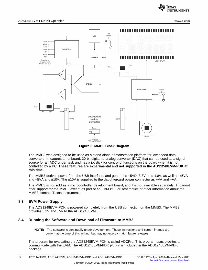
The MMB3 is a Modular EVM System motherboard. It is designed around the MSP430F449, a low-powermicrocontroller from Texas Instruments. Figure 8 shows a block diagram of the MMB3.
11SBAU142B–April 2009–Revised May 2011 ADS1148EVM, ADS1248EVM, ADS1148EVM-PDK, and ADS1248EVM-PDKSubmit Documentation Feedback
Copyright © 2009–2011, Texas Instruments Incorporated
+5VA
-5VA
+5VD
+3.3V
+1.8V
+10V
-10V
PWR & VREF
USB
USB
RESET
DAC1220
TUSB3410
MSP430F449
+1
-1
DAC
IN OUT
Analog
Daughtercard
Modular
Connectors
Power
Power from
PWR & VREF Block
Serial
Joystick
RESET
OPER
LCD DISPLAY
BSL
2.5V
Supplied to
Daughtercard
Power Connector
ADS1248EVM-PDK Kit Operation www.ti.com
Figure 8. MMB3 Block Diagram
The MMB3 was designed to be used as a stand-alone demonstration platform for low-speed dataconverters. It features an onboard, 20-bit digital-to-analog converter (DAC) that can be used as a signalsource for an ADC under test, and has a joystick for control of functions on the board when it is notcontrolled by a PC. These features are experimental and not supported in the ADS1248EVM-PDK atthis time.
The MMB3 derives power from the USB interface, and generates +5VD, 3.3V, and 1.8V, as well as +5VAand –5VA and ±10V. The ±10V is supplied to the daughtercard power connector as +VA and –VA.
The MMB3 is not sold as a microcontroller development board, and it is not available separately. TI cannotoffer support for the MMB3 except as part of an EVM kit. For schematics or other information about theMMB3, contact Texas Instruments.
8.3 EVM Power Supply
The ADS1248EVM-PDK is powered completely from the USB connection on the MMB3. The MMB3provides 3.3V and ±5V to the ADS1248EVM.
8.4 Running the Software and Download of Firmware to MMB3
NOTE: The software is continually under development. These instructions and screen images arecurrent at the time of this writing, but may not exactly match future releases.
The program for evaluating the ADS1248EVM-PDK is called ADCPro. This program uses plug-ins tocommunicate with the EVM. The ADS1248EVM-PDK plug-in is included in the ADS1248EVM-PDKpackage.
12 ADS1148EVM, ADS1248EVM, ADS1148EVM-PDK, and ADS1248EVM-PDK SBAU142B–April 2009–Revised May 2011Submit Documentation Feedback
Copyright © 2009–2011, Texas Instruments Incorporated

www.ti.com ADS1248EVM-PDK Kit Operation
The program currently runs only on Microsoft Windows platforms of Windows XP; Windows Vista is NOTsupported.
If this is the first time installing ADCPro and plug-ins, follow these procedures to run ADCPro and performany necessary firmware installations. Make sure the ADCPro software and device plug-in software areinstalled from the CD-ROM as described in Section 8.1, Installing the ADCPro Software.
Step 1. Start the software by selecting ADCPro from the Windows Start menu. The screen in Figure 9appears.
Figure 9. ADCPro Software Start-up Display Window
13SBAU142B–April 2009–Revised May 2011 ADS1148EVM, ADS1248EVM, ADS1148EVM-PDK, and ADS1248EVM-PDKSubmit Documentation Feedback
Copyright © 2009–2011, Texas Instruments Incorporated

ADS1248EVM-PDK Kit Operation www.ti.com
breakStep 2. Select ADS1248EVM from the EVM drop-down menu. The ADS1248EVM-PDK plug-in
appears in the left pane, as shown in Figure 10.
Figure 10. ADS1248EVM-PDK Plug-In Display Window
Step 3. The ADS1248EVM-PDK plug-in window has a status area at the top of the screen. When theplug-in is first loaded, the plug-in searches for the board. You will see a series of messagesin the status area indicating this action.
14 ADS1148EVM, ADS1248EVM, ADS1148EVM-PDK, and ADS1248EVM-PDK SBAU142B–April 2009–Revised May 2011Submit Documentation Feedback
Copyright © 2009–2011, Texas Instruments Incorporated

www.ti.com ADS1248EVM-PDK Kit Operation
breakStep 4. If the plug-in cannot connect to the EVM, you will see a window as shown in Figure 11. This
message may indicate that the firmware is not loaded on the MMB3. You may select RetryAuto Connect; if that action fails, select Retry Manual Connect and specify the COM port tobe used.
Figure 11. Connection Timeout
Step 5. The plug-in detects whether or not the board has the correct firmware loaded. The first timeyou use the ADS1248EVM-PDK, the firmware for the MMB3 may need to be downloaded tothe MMB3. If the firmware needs to be loaded, you will see a screen as shown in Figure 12.
Figure 12. Firmware Download Message Box
15SBAU142B–April 2009–Revised May 2011 ADS1148EVM, ADS1248EVM, ADS1148EVM-PDK, and ADS1248EVM-PDKSubmit Documentation Feedback
Copyright © 2009–2011, Texas Instruments Incorporated

ADS1248EVM-PDK Kit Operation www.ti.com
Switch the BSL switch (SW4) on the MMB3 to the BSL position (to the left) as instructed, then pressOK. The plug-in will download the firmware to the MMB3. This operation may take a couple of minutes,so the progress is updated in the message at the top of the ADS1248 plug-in window (as Figure 13shows). The firmware is saved in flash memory on the MMB3, so this operation should only need to beperformed once.
Figure 13. Firmware Download Progress Indicator
16 ADS1148EVM, ADS1248EVM, ADS1148EVM-PDK, and ADS1248EVM-PDK SBAU142B–April 2009–Revised May 2011Submit Documentation Feedback
Copyright © 2009–2011, Texas Instruments Incorporated

www.ti.com Evaluating Performance with the ADCPro Software
When the firmware download completes, the message box shown in Figure 14 appears. Follow theon-screen instructions and the plug-in should now connect to the EVM.
Figure 14. Firmware Download Complete Message Box
9 Evaluating Performance with the ADCPro Software
The evaluation software is based on ADCPro, a program that operates using a variety of plug-ins. To useADCPro, load an EVM plug-in and a test plug-in. To load an EVM plug-in, select it from the EVM menu.To load a test plug-in, select it from the Test menu. To unload a plug-in, select the Unload option from thecorresponding menu.
Only one of each kind of plug-in can be loaded at a time. If you select a different plug-in, the previousplug-in is unloaded.
9.1 Using the ADS1248EVM-PDK Plug-in
The ADS1248EVM-PDK plug-in for ADCPro provides complete control over all settings of the ADS1248. Itconsists of a tabbed interface (see Figure 16), with different functions available on different tabs. Thesecontrols are described in this section.
You can adjust the ADS1248EVM settings when you are not acquiring data. During acquisition, allcontrols are disabled and settings may not be changed.
When you change a setting on the ADS1248EVM plug-in, the setting immediately updates on the board.
Settings on the ADS1248EVM correspond to settings described in the ADS1248 data sheet (available fordownload at www.ti.com) for details.
The ADS1248EVM-PDK plug-in has a tabbed interface, with five different tabs to control the functions ofthe ADS1248. These tabs are described below.
17SBAU142B–April 2009–Revised May 2011 ADS1148EVM, ADS1248EVM, ADS1148EVM-PDK, and ADS1248EVM-PDKSubmit Documentation Feedback
Copyright © 2009–2011, Texas Instruments Incorporated

(MUXCAL = 001)
System Monitors
Temperature
DiodeVREFP
VREFN
VREFP1/4
VREFN1/4
VREFP0/4
VREFN0/4
AVDD/4
AVSS/4
DVDD/4
DVSS/4ADS1248 Only
ADS1247/48 Only
VBIAS
AIN0
AIN1
VBIAS
AIN2
VBIAS
AIN3
VBIAS
AIN4
VBIAS
AIN5
VBIAS
AIN6
VBIAS
AIN7
AVDD
IDAC1IDAC2
AVDD
VBIAS
PGA
AINP
AVSS
AVDD
Burnout Current Source
(0.5 A, 2 A, 10m m mA)
Burnout Current Source
(0.5 A, 2 A, 10m m mA)
AINN
To
ADC
AVSS
AVSS
AVSS
AVSS
AVSS
AVSS
AVSS
AVSS
AVDD
AVDD
AVDD
AVDD
AVDD
AVDD
AVDD
AVDD
AVDD AVDD
Evaluating Performance with the ADCPro Software www.ti.com
9.1.1 I/O Config Tab
This tab is the primary tab that controls the function of the multiplexer in the ADS1248. Recall that theADS1248 multiplexer is configured as shown in Figure 15. By default, all channels are set as analoginputs; the IDACs are not routed to any channel and the IDAC controls are disabled. These controls areenabled when the correct IDAC settings are made on the Power & Ref tab (see Section 9.1.3).
Figure 15. ADS1248 Multiplexer
The radio buttons at the far right of the panel (see Figure 16) select which pair of inputs are connected tothe PGA. Note that you may select the same input for both the positive (AINP) and negative (AINN) input;this configuration is often selected to perform a noise test on the ADC itself.
18 ADS1148EVM, ADS1248EVM, ADS1148EVM-PDK, and ADS1248EVM-PDK SBAU142B–April 2009–Revised May 2011Submit Documentation Feedback
Copyright © 2009–2011, Texas Instruments Incorporated

www.ti.com Evaluating Performance with the ADCPro Software
Input pins AIN2-AIN7 can be selected to be an analog input or GPIO. If an input is to be used as a GPIO,check the GPIO box as shown in Figure 16.
Figure 16. I/O Config Tab
When an input is selected as a GPIO, its label turns green and the IDAC controls for that channel aredisabled.
19SBAU142B–April 2009–Revised May 2011 ADS1148EVM, ADS1248EVM, ADS1148EVM-PDK, and ADS1248EVM-PDKSubmit Documentation Feedback
Copyright © 2009–2011, Texas Instruments Incorporated

Evaluating Performance with the ADCPro Software www.ti.com
Each input channel can also have a VBIAS applied to it. Checking the VBIAS box on a channel appliesthe VBIAS voltage, which is approximately half the value of the supply. You can test this option as shownin Figure 17, using one channel tied to a value close to ground (make sure you observe thecommon-mode restrictions listed in the ADS1248 product data sheet) as a reference for this signal.
Figure 17. Enabling VBIAS on a Channel
The System Monitor button allows you to access the internal system monitor channels of the ADS1248.When pressed, this button disables the other analog input channel controls, and the system monitorchannel selections are enabled. You can select Offset, Gain, Temperature, VREF1, VREF0, AVDD, orDVDD as the channel to convert. Note that some of these channels are scaled by a factor when read;refer to the ADS1248 product data sheet to determine these factors.
The PGA Gain control sets the PGA gain, and the Data Rate control sets the data rate for the device.Note that the data rate can go quite low; therefore, if the block size is large, the time it takes to collect ablock of data can be quite long. It is advisable to first test collection at the higher data rates. Once a test isknown to work properly, drop to a lower data rate and allow sufficient time to collect the data.
The BCS control sets the current level of the burnout current sources; it may be set to Off, or to 0.5μA,2μA, or 10μA.
The Power Down control powers down the ADS1248. Note that no data can be collected if the PowerDown button is activated.
20 ADS1148EVM, ADS1248EVM, ADS1148EVM-PDK, and ADS1248EVM-PDK SBAU142B–April 2009–Revised May 2011Submit Documentation Feedback
Copyright © 2009–2011, Texas Instruments Incorporated

www.ti.com Evaluating Performance with the ADCPro Software
9.1.2 GPIO Tab
When an input is selected to be a GPIO, its controls are enabled on the GPIO tab, shown in Figure 18. Bydefault, the GPIOs are enabled as inputs. Pressing the Input button reads the state of the enabled inputs;if the input is high, the corresponding light turns green.
Figure 18. GPIO Tab
21SBAU142B–April 2009–Revised May 2011 ADS1148EVM, ADS1248EVM, ADS1148EVM-PDK, and ADS1248EVM-PDKSubmit Documentation Feedback
Copyright © 2009–2011, Texas Instruments Incorporated

Evaluating Performance with the ADCPro Software www.ti.com
To make the GPIO an output, the toggle switch can be switched to output mode, as shown in Figure 19.
Figure 19. GPIO Set to Output Mode
22 ADS1148EVM, ADS1248EVM, ADS1148EVM-PDK, and ADS1248EVM-PDK SBAU142B–April 2009–Revised May 2011Submit Documentation Feedback
Copyright © 2009–2011, Texas Instruments Incorporated

www.ti.com Evaluating Performance with the ADCPro Software
With the GPIO configured as an output, the pushbutton switch controls the state of the output pin. Whenpressed (as illustrated in Figure 20), the button lights up and the GPIO is set to a high state; when theswitch is dark (as Figure 19 shows), the GPIO is in a low state.
Figure 20. GPIO Output Set to High
23SBAU142B–April 2009–Revised May 2011 ADS1148EVM, ADS1248EVM, ADS1148EVM-PDK, and ADS1248EVM-PDKSubmit Documentation Feedback
Copyright © 2009–2011, Texas Instruments Incorporated

Evaluating Performance with the ADCPro Software www.ti.com
9.1.3 Power & Ref Tab
The Power & Ref tab is shown in Figure 21. This tab controls the selection of the power-supply mode,reference sources, and IDACs.
Figure 21. Power & Ref Tab
Note that with the Internal Reference off, the IDAC controls are disabled, because the IDACs cannot beused unless the internal reference is turned on.
24 ADS1148EVM, ADS1248EVM, ADS1148EVM-PDK, and ADS1248EVM-PDK SBAU142B–April 2009–Revised May 2011Submit Documentation Feedback
Copyright © 2009–2011, Texas Instruments Incorporated

www.ti.com Evaluating Performance with the ADCPro Software
The Power Supply control selects between single supply (+5V) mode and bipolar supply (±2.5V) mode.The EVM draws its supply voltages from the MMB3 motherboard, and has onboard circuitry to selectbetween the +5V and bipolar supplies.
The Reference Select control selects between VREF0, VREF1, and the Internal Reference. WhenVREF1 is selected, the VREF value is set to 2.048V, with switch S1 set to BUFF. S1 should not be set tothe AVDD position, in order to prevent the reference from exceeding the maximum specified input.
There are two checkboxes that, when enabled, allow the REF0P and REF0N pins to be selected asGPIOs. These checkboxes are enabled only in modes that allow these pins to be used as GPIOs.
The Internal Reference control selects whether the reference is off, on, or follows the START signal (referto the ADS1248 data sheet for more details on these choices). When the internal reference is enabled, theIDAC controls are enabled as well, because the IDACs cannot function unless the internal reference isturned on. Note that the internal reference does not necessarily have to be used as the ADC reference inorder to use the IDACs, but it does need to be turned on.
The IDAC Magnitude control sets the amount of current each of the two IDACs provide.
The IDAC0 and IDAC 1 Routing controls allow you to specify where the IDAC0 or IDAC1 current go: toeither the IEXC1 or IEXC2 pins, or to the Analog inputs, or you may turn the IDAC off. If the AIN button isselected, this option enables the corresponding IDAC controls on the I/O Config tab.
25SBAU142B–April 2009–Revised May 2011 ADS1148EVM, ADS1248EVM, ADS1148EVM-PDK, and ADS1248EVM-PDKSubmit Documentation Feedback
Copyright © 2009–2011, Texas Instruments Incorporated
Evaluating Performance with the ADCPro Software www.ti.com
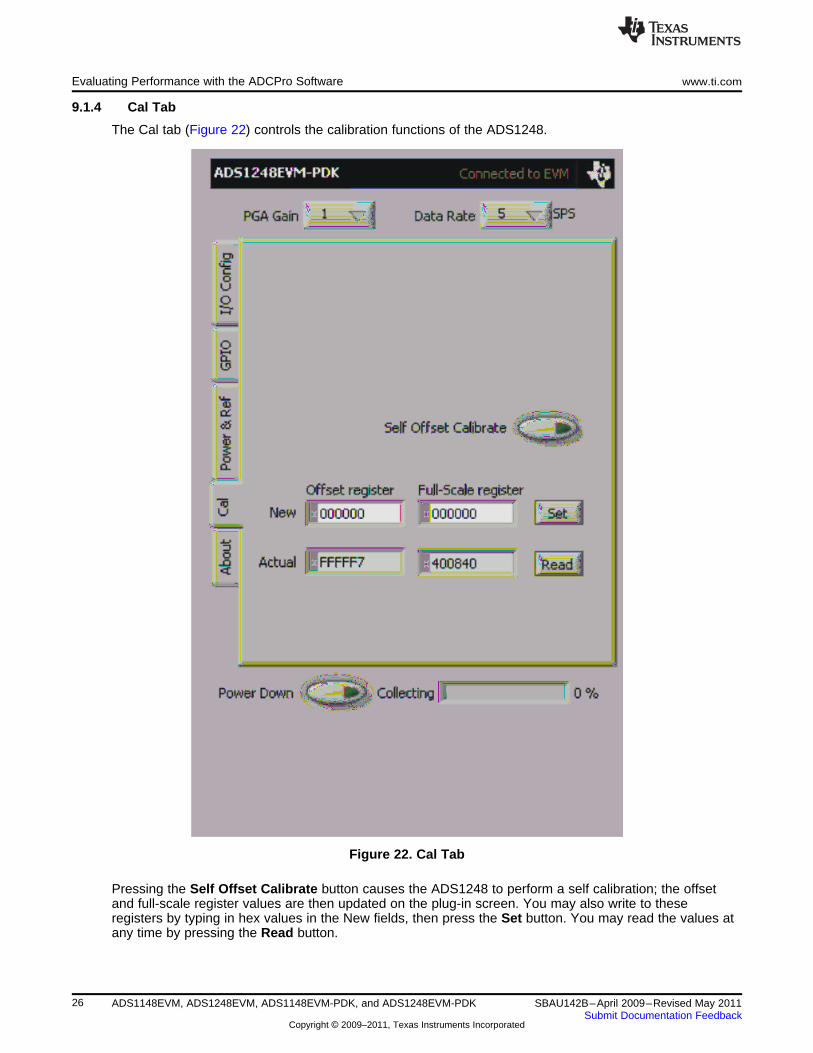
9.1.4 Cal Tab
The Cal tab (Figure 22) controls the calibration functions of the ADS1248.
Figure 22. Cal Tab
Pressing the Self Offset Calibrate button causes the ADS1248 to perform a self calibration; the offsetand full-scale register values are then updated on the plug-in screen. You may also write to theseregisters by typing in hex values in the New fields, then press the Set button. You may read the values atany time by pressing the Read button.
26 ADS1148EVM, ADS1248EVM, ADS1148EVM-PDK, and ADS1248EVM-PDK SBAU142B–April 2009–Revised May 2011Submit Documentation Feedback
Copyright © 2009–2011, Texas Instruments Incorporated

www.ti.com Evaluating Performance with the ADCPro Software
9.1.5 About Tab
The About tab displays information about the EVM and software, as shown in Figure 23.
Figure 23. About Tab
The Plugin Version and Firmware Version indicators show the version numbers of the plug-in andfirmware code, respectively.
The ID indicator shows the value of the ID [3:0] bits in the ADS1248 ID register.
The Notes indicator may show relevant notes about the plug-in or firmware code, if there are any.
27SBAU142B–April 2009–Revised May 2011 ADS1148EVM, ADS1248EVM, ADS1148EVM-PDK, and ADS1248EVM-PDKSubmit Documentation Feedback
Copyright © 2009–2011, Texas Instruments Incorporated

Evaluating Performance with the ADCPro Software www.ti.com
9.1.6 Collecting Data
Once you have configured the ADS1248 for your test scenario, press the ADCPro Acquire button to startthe collection of the number of datapoints specified in the Test plug-in Block Size control. TheADS1248EVM-PDK plug-in disables all the front panel controls while acquiring, and displays a progressbar as shown in Figure 24.
Figure 24. Progress Bar While Collecting Data
For more information on testing analog-to-digital converters in general and using ADCPro and testplug-ins, refer to the ADCPro User Guide.
28 ADS1148EVM, ADS1248EVM, ADS1148EVM-PDK, and ADS1248EVM-PDK SBAU142B–April 2009–Revised May 2011Submit Documentation Feedback
Copyright © 2009–2011, Texas Instruments Incorporated
www.ti.com Schematics and Layout
9.2 Troubleshooting
If the ADS1248EVM plug-in cannot find the ADS1248EVM-PDK, press the USB RESET button on theMMB3 (refer to Figure 6) and try again.
If ADCPro stops responding while the ADS1248EVM-PDK is connected, try unplugging the USB cablefrom the PDK. Unload and reload the plug-in before reapplying power to the PDK.
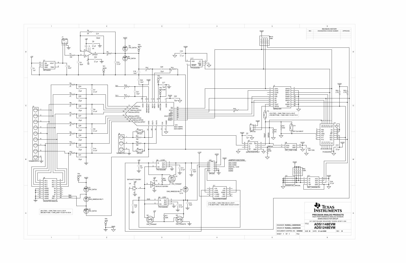
10 Schematics and Layout
Schematics for the ADS1148EVM and ADS1248EVM are appended to this user's guide. The bill ofmaterials is provided in Table 7.
10.1 Bill of Materials
NOTE: All components should be compliant with the European Union Restriction on Use ofHazardous Substances (RoHS) Directive. Some part numbers may be either leaded orRoHS. Verify that purchased components are RoHS-compliant. (For more information aboutTI's position on RoHS compliance, see the Quality and Eco-Info information on the TI website.)
Table 7. ADS1148EVM/ADS1248EVM Bill of Materials
Item No. Qty Value Ref Des Description Vendor Part Number
1 1 N/A ADS1248 EVM PWB Texas 6496961Instruments
2 4 1μF C1-C3, C33 Capacitor, X7R Ceramic 1μF ±10%, 16WV, TDK C1608X7R1C105KTSize = 0603
3 2 22μF C4, C5 Capacitor, X5R Ceramic 22μF ±20%, TDK C3225X5R1C226MT16WV, Size = 1210
4 12 0.1μF C6-C13, C15, C34, Capacitor, X7R Ceramic 0.1μF ±10%, TDK C1608X7R1E104KTC35, C36 25WV, Size = 0603
5 1 0.15μF C14 Capacitor, X7R Ceramic 0.15μF ±10%, Murata GRM188R71C154KA16WV, Size = 0603 01D
6 8 10μF C16-C23 Capacitor, X5R Ceramic 10μF ±20%, TDK C2012X5R0J106MT6.3WV, Size = 0805
7 8 47pF C24-C31 Capacitor, C0G Ceramic 47pF ±5%, 50WV, TDK C1608C0G1H470JTSize = 0603
8 1 10nF C32 Capacitor, C0G Ceramic 10nF ±5%, 25WV, TDK C1608C0G1E103JTSize = 0603
9 4 D1, D2, D5, D6 DIODE SCHOTTKY 30V 200MA SOT-23 Fairchild BAT54
10 2 D3, D4 5.1V, Zener Diode On MMBZ5231BLT1GSemiconductor
11 2 J1, J2 Header Strip, 3-pin ( ) Samtec TSW-103-07-L-S
12 1 J4 Terminal Block, 9-position On Shore ED555/9DSTechnology
13 4 J5, J6, J13, J14 Header Strip, 2-pin ( ) Samtec TSW-102-07-L-S
14 2 J7A, J8A 20-pin SMT Plug Samtec TSM-110-01-L-DV-P
15 2 J7B, J8B 20-pin SMT Socket Samtec SSW-110-22-F-D-VS-K
16 1 J9 Terminal Block, 3 position On Shore ED555/3DSTechnology
17 1 J10 Header Strip, 10-pin ( ) Samtec TSW-105-07-L-D
18 1 J11A 10-pin SMT Plug Samtec TSM-105-01-L-DV-P
19 1 J11B 10-pin SMT Socket Samtec SSW-105-22-F-D-VS-K
20 0 J12 Header Strip, 6-pin ( )
21 2 Q1, Q2 MOSFET, P-Channel, 2.5V Fairchild FDN302P
22 1 Q3 Enhancement Mode FET, N-Channel Fairchild FDN337N
23 1 100kΩ RA1 Resistor, 8 Thick Film Chip Array 100kΩ, CTS 745C101104JPTR5%, 63mW
29SBAU142B–April 2009–Revised May 2011 ADS1148EVM, ADS1248EVM, ADS1148EVM-PDK, and ADS1248EVM-PDKSubmit Documentation Feedback
Copyright © 2009–2011, Texas Instruments Incorporated
Revision History www.ti.com
Table 7. ADS1148EVM/ADS1248EVM Bill of Materials (continued)
Item No. Qty Value Ref Des Description Vendor Part Number
24 0 RA2 Resistor, Chip Array 4 Independent Bus100kΩ, 5%, 1/16W, SMD
25 1 10kΩ R1 Resistor, Thick Film Chip 10kΩ, 5%, 1/10W, Panasonic ERJ-3GEYJ103VSize = 0603
26 1 2kΩ R2 Resistor, Thick Film Chip 2kΩ, 1%, 1/16W, Panasonic ERJ-3EKF2001VSize = 0603
27 10 47Ω R3-R12 Resistor, Thick Film Chip 47Ω, 5%, 1/10W, Panasonic ERJ-3GEYJ470VSize = 0603
28 2 100kΩ R13, R23 Resistor, Thick Film Chip 100kΩ, 5%, Panasonic ERJ-3GEYJ104V1/10W, Size = 0603
29 4 0Ω R14, R15, R16, R17 Resistor, Thick Film Chip 0Ω, 5%, 1/10W, Panasonic ERJ-3GEY0R00VSize = 0603
30 1 47kΩ R18 Resistor, Thick Film Chip 47kΩ, 5%, 1/10W, Panasonic ERJ-3GEYJ473VSize = 0603
31 2 470kΩ R19, R20 Resistor, Thick Film Chip 470kΩ, 5%, Panasonic ERJ-3GEYJ474V1/10W, Size = 0603
32 2 100Ω R21, R22 Resistor, Thick Film Chip 100Ω, 5%, 1/10W, Panasonic ERJ-3GEYJ101VSize = 0603
33 2 2.7kΩ R24, R25 Resistor, Thick Film Chip 2.7kΩ, 5%, Panasonic ERJ-3GEYJ272V1/10W, Size = 0603
34 1 S1 Switch, Mini Slide, SPDT NKK SS12SDP2
35 0 TP1-TP5 PCB Test Point, Mini Loop, Through-Hole
36 1 TP6 PCB Test Point, Large Loop, Through-Hole Keystone 5011Electronics
37 1 U1 Precision Voltage Reference, 2.048V Texas REF5020IDInstruments
38 1 U2 Precision Operational Amplifier Texas OPA227UInstruments
39 1 U3 Texas PCA9535RGE16-Bit I2C I/O ExpanderInstruments
40 1 U4 Inverter, Single Gate Texas SN74AHCT1G04DBVInstruments R
41 1 U5 Buffer, Open Drain, Single Gate Texas SN74LVC1G07DBVRInstruments G4
42 1 U6 LDO Voltage Regulator, 2.5V, 100mA Texas TPS79225DBVRG4Instruments
43 1 U7 Single, 2-Line to 1 Data Selector/Multiplexer Texas SN74LVC2G157DCTInstruments
44 0 U8 3.3 V Oscillator
45 1 U9 LDO Voltage Regulator, 2.5V, 200mA Texas TPS72325DBVTG4Instruments
46 1 U10 Precision Delta-Sigma ADC, 24-bit/16-bit Texas ADS1248IPW/ADS11Instruments 48IPW
47 1 U11 EEPROM, 1.8V, 256k Microchip 24AA256-I/ST
48 1 U12 Supervisor, 2.64V Threshold Texas TPS3836L30DBVTInstruments
49 10 N/A Shorting Blocks Samtec SNT-100-BK-T
Revision History
Changes from A Revision (July, 2009) to B Revision .................................................................................................... Page
• Updated Table 3 .......................................................................................................................... 5
NOTE: Page numbers for previous revisions may differ from page numbers in the current version.
30 Revision History SBAU142B–April 2009–Revised May 2011Submit Documentation Feedback
Copyright © 2009–2011, Texas Instruments Incorporated

1 2 3 4 5 6
A
B
C
D
654321
D
C
B
Ati
5411 EAST WILLIAMS BOULEVARD, TUCSON, AZ 85711 USA
TITLE
SHEET OF FILE
SIZE DATE REV
DRAWN BY
ENGINEER
REVISION HISTORYREV ENGINEERING CHANGE NUMBER APPROVED
B
PRECISION ANALOG PRODUCTSHIGH-PERFORMANCE ANALOG DIVISION
SEMICONDUCTOR GROUP
DOCUMENT CONTROL NO.
R2
2K
+5V
-5V
+5V
R3
47
C14
150nF
C150.1uF
C6
0.1uF
C11uF
R1
10K
1 2 3
J1JPR-1X3
C522uF
GND
TP6GND
CNTL1
CLKX3
CLKR5
FSX7
FSR9
DX11
DR13
INT15
TOUT17
GPIO519
GPIO02
DGND4
GPIO16
GPIO28
DGND10
GPIO312
GPIO414
SCL16
DGND18
SDA20
J7
SERIALHDR
OBCLK EOH1
GND2
OUT3
VCC4
U8
CRY_C3391-4.096
DVDD
C3210nF C0G
A1
B2
Y3
GND4
Y5
A/B6
G7
VCC8
U7
SN74LVC2G157DCT
R20470K
R1847K
R19470K
TOU
T
GP
IO5
J7A (TOP) = SAM_TSM-110-01-L-DV-PJ7B (BOTTOM) = SAM_SSW-110-22-F-D-VS
DVDD
P00
1P
012
P02
3P
034
P04
5P
056
P067
P078
GND9
P1010
P1111
P1212
P13
13
P14
14
P15
15
P16
16
P17
17
A0
18
SCL19
SDA20
VCC21
INT22
A123
A224
U3
PCA9535RGE
C12
0.1uF
DVDD
D1FRC_BAT54
D2FRC_BAT54
D3ONS_MMBZ5231BLT1
VIN2
VOUT6
TRIM5
GND4
TEMP3
U1
REF5020ID
AVDD
A0(+)2
A1(+)4
A2(+)6
A3(+)8
A410
A512
A614
A716
REF-18
REF+20
A0(-)1
A1(-)3
A2(-)5
A3(-)7
AGND9
AGND11
AGND13
VCOM15
AGND17
AGND19
J8
DAUGHTER-ANALOG
J8A (TOP) = SAM_TSM-110-01-L-DV-PJ8B (BOTTOM) = SAM_SSW-110-22-F-D-VS-K
IN1
GND2
EN3
OUT5
BYP4
U6
TPS79225DBV
Q1
FRC_FDN302P2 4
53
U5
SN74LVC1G07DBV
R23100K
+5V
+5V
Q3
FRC_FDN337N
+5V
2 4
53
U4
SN74AHCT1G04DBV+5V
+3.3V
-VA2
-5VA4
AGND6
VD18
+5VD10
+VA1
+5VA3
DGND5
+1.8VD7
+3.3VD9
J11
DAUGHTER-POWER
ADC AVDDADC AVSSDIGITAL=3.3VDGNDAGND
DVDDJUMPER FUNCTIONS
D4ONS_MMBZ5231BLT1
J11A (TOP) = SAM_TSM-105-01-L-DV-PJ11B (BOTTOM) = SAM_SSW-105-22-F-D-VS-K
IN2
GND1
EN3
OUT5
BYP4
U9
TPS72325DBV
Q2
FRC_FDN302P
R13100K
C1610uF
AVDD
AVDD
DVDD
C331uF
-5VA
5.1V
-2.5V
+2.5V
C23
10uF
C2210uF
C20
10uF
R150
R140
R10
47
123
J2
JPR-1X3
2
36
74
1 8
U2
OPA227
Ref-Ref+
DVDD
C422uF
C110.1uF C18
10uF
C1910uFC13
0.1uF
RUSSELL ANDERSON
RUSSELL ANDERSON
6496962
1 1
11-Feb-2009
ADS1148EVM
A
C21uF
1 23 45 67 89 10
J10
JPR-2X5
C3
1uF
DVDD
CLK
3
SCLK28
DOUT/DRDY26
DRDY25
DIN27
CS24
AIN3/Iexc/GPIO318
AIN6/Iexc/GPIO615
AIN1/Iexc12
RE
F0N
/GP
IO1
6
START23
IOU
T219
AIN0/Iexc11
AIN2/Iexc/GPIO217
AV
DD
22
AV
SS
21
VR
EFC
OM
10V
RE
FP9
IOU
T120
RESET4
RE
F1N
8
DV
DD
1D
GN
D2
RE
F0P
/GP
IO0
5
AIN7/Iexc/GPIO716
AIN4/Iexc/GPIO413
AIN5/Iexc/GPIO514
RE
F1P
7
U10ADS1148IPW
C2110uF
R16
0
R17
0
Ref+
Ref-
R4
47
R5
47
R6
47
R7
47
R8
47
R9
47
R11
47
R12
47
C26
47pF
C25
47pF
C24
47pF
C27
47pF
C28
47pF
C29
47pF
C30
47pF
C31
47pF
C70.1uF
C80.1uF
C90.1uF
C100.1uF
C17
10uF
TP3Int REF
TP1AVSS
TP4AVDD
TP2REFP
S1
AVDD
TP5REFCOM
R21
100
R22
100
1 2J5
JPR-2X1
1 2J6
JPR-2X1
1
2
3
J9
TERMBLOCK-3
RA1A100K
-5V
1
2
3
4
5
6
7
8
9
J4
TERMBLOCK-9
C34
0.1uF
D5FRC_BAT54
D6FRC_BAT54
A01
A12
GND4
SDA5
SCL6
WP7
VCC8
A23
U11
MCP_24AA256-I/ST
C350.1uF
DVDD
DVDD
246
135
J12
HEADER-3X2
RA2100K
R242.7K
R252.7K
DVDD
12 J13
12
J14
EXT CLK INPUT
C36
0.1uF
DVDD
VDD5
RESET4
MR3
CT1
GND2
U12
TPS3836DBV
ADS1248EVM
ADS1248IPW
1 2 3 4 5 6
A
B
C
D
654321
D
C
B
Ati
5411 EAST WILLIAMS BOULEVARD, TUCSON, AZ 85711 USA
TITLE
SHEET OF FILE
SIZE DATE REV
DRAWN BY
ENGINEER
REVISION HISTORYREV ENGINEERING CHANGE NUMBER APPROVED
B
PRECISION ANALOG PRODUCTSHIGH-PERFORMANCE ANALOG DIVISION
SEMICONDUCTOR GROUP
DOCUMENT CONTROL NO.
R2
2K
+5V
-5V
+5V
R3
47
C14
150nF
C150.1uF
C6
0.1uF
C11uF
R1
10K
1 2 3
J1JPR-1X3
C522uF
GND
TP6GND
CNTL1
CLKX3
CLKR5
FSX7
FSR9
DX11
DR13
INT15
TOUT17
GPIO519
GPIO02
DGND4
GPIO16
GPIO28
DGND10
GPIO312
GPIO414
SCL16
DGND18
SDA20
J7
SERIALHDR
OBCLK EOH1
GND2
OUT3
VCC4
U8
CRY_C3391-4.096
DVDD
C3210nF C0G
A1
B2
Y3
GND4
Y5
A/B6
G7
VCC8
U7
SN74LVC2G157DCT
R20470K
R1847K
R19470K
TOU
T
GP
IO5
J7A (TOP) = SAM_TSM-110-01-L-DV-PJ7B (BOTTOM) = SAM_SSW-110-22-F-D-VS
DVDD
P00
1P
012
P02
3P
034
P04
5P
056
P067
P078
GND9
P1010
P1111
P1212
P13
13
P14
14
P15
15
P16
16
P17
17
A0
18
SCL19
SDA20
VCC21
INT22
A123
A224
U3
PCA9535RGE
C12
0.1uF
DVDD
D1FRC_BAT54
D2FRC_BAT54
D3ONS_MMBZ5231BLT1
VIN2
VOUT6
TRIM5
GND4
TEMP3
U1
REF5020ID
AVDD
A0(+)2
A1(+)4
A2(+)6
A3(+)8
A410
A512
A614
A716
REF-18
REF+20
A0(-)1
A1(-)3
A2(-)5
A3(-)7
AGND9
AGND11
AGND13
VCOM15
AGND17
AGND19
J8
DAUGHTER-ANALOG
J8A (TOP) = SAM_TSM-110-01-L-DV-PJ8B (BOTTOM) = SAM_SSW-110-22-F-D-VS-K
IN1
GND2
EN3
OUT5
BYP4
U6
TPS79225DBV
Q1
FRC_FDN302P2 4
53
U5
SN74LVC1G07DBV
R23100K
+5V
+5V
Q3
FRC_FDN337N
+5V
2 4
53
U4
SN74AHCT1G04DBV+5V
+3.3V
-VA2
-5VA4
AGND6
VD18
+5VD10
+VA1
+5VA3
DGND5
+1.8VD7
+3.3VD9
J11
DAUGHTER-POWER
ADC AVDDADC AVSSDIGITAL=3.3VDGNDAGND
DVDDJUMPER FUNCTIONS
D4ONS_MMBZ5231BLT1
J11A (TOP) = SAM_TSM-105-01-L-DV-PJ11B (BOTTOM) = SAM_SSW-105-22-F-D-VS-K
IN2
GND1
EN3
OUT5
BYP4
U9
TPS72325DBV
Q2
FRC_FDN302P
R13100K
C1610uF
AVDD
AVDD
DVDD
C331uF
-5VA
5.1V
-2.5V
+2.5V
C23
10uF
C2210uF
C20
10uF
R15
0
R14
0
R10
47
123
J2
JPR-1X3
2
36
74
1 8
U2
OPA227
Ref-Ref+
DVDD
C422uF
C110.1uF C18
10uF
C1910uFC13
0.1uF
RUSSELL ANDERSON
RUSSELL ANDERSON
6496962
1 1
31-Jul-2009
ADS1148EVM
B
C21uF
1 23 45 67 89 10
J10
JPR-2X5
C3
1uF
DVDD
CLK
3
SCLK28
DOUT/DRDY26
DRDY25
DIN27
CS24
AIN3/Iexc/GPIO318
AIN6/Iexc/GPIO615
AIN1/Iexc12
RE
F0N
/GP
IO1
6
START23
IOU
T219
AIN0/Iexc11
AIN2/Iexc/GPIO217
AV
DD
22
AV
SS
21
VR
EFC
OM
10V
RE
FP9
IOU
T120
RESET4
RE
F1N
8
DV
DD
1D
GN
D2
RE
F0P
/GP
IO0
5
AIN7/Iexc/GPIO716
AIN4/Iexc/GPIO413
AIN5/Iexc/GPIO514
RE
F1P
7
U10ADS1148IPW
C2110uF
R16
0
R17
0
Ref+
Ref-
R4
47
R5
47
R6
47
R7
47
R8
47
R9
47
R11
47
R12
47
C26
47pF
C25
47pF
C24
47pF
C27
47pF
C28
47pF
C29
47pF
C30
47pF
C31
47pF
C70.1uF
C80.1uF
C90.1uF
C100.1uF
C17
10uF
TP3Int REF
TP1AVSS
TP4AVDD
TP2REFP
AVDD
TP5REFCOM
R21
100
R22
100
1 2J5
JPR-2X1
1 2J6
JPR-2X1
1
2
3
J9
TERMBLOCK-3
RA1A100K
-5V
1
2
3
4
5
6
7
8
9
J4
TERMBLOCK-9
C34
0.1uF
D5FRC_BAT54
D6FRC_BAT54
A01
A12
GND4
SDA5
SCL6
WP7
VCC8
A23
U11
MCP_24AA256-I/ST
C350.1uF
DVDD
DVDD
RA2100K
R242.7K
R252.7K
DVDD
12 J13
12
J14
EXT CLK INPUT
C36
0.1uF
DVDD
VDD5
RESET4
MR3
CT1
GND2
U12
TPS3836DBV
ADS1248EVM
ADS1248IPW
246
135
J12
HEADER-3X2_SPECIAL

Evaluation Board/Kit Important Notice
Texas Instruments (TI) provides the enclosed product(s) under the following conditions:
This evaluation board/kit is intended for use for ENGINEERING DEVELOPMENT, DEMONSTRATION, OR EVALUATIONPURPOSES ONLY and is not considered by TI to be a finished end-product fit for general consumer use. Persons handling theproduct(s) must have electronics training and observe good engineering practice standards. As such, the goods being provided arenot intended to be complete in terms of required design-, marketing-, and/or manufacturing-related protective considerations,including product safety and environmental measures typically found in end products that incorporate such semiconductorcomponents or circuit boards. This evaluation board/kit does not fall within the scope of the European Union directives regardingelectromagnetic compatibility, restricted substances (RoHS), recycling (WEEE), FCC, CE or UL, and therefore may not meet thetechnical requirements of these directives or other related directives.
Should this evaluation board/kit not meet the specifications indicated in the User’s Guide, the board/kit may be returned within 30days from the date of delivery for a full refund. THE FOREGOING WARRANTY IS THE EXCLUSIVE WARRANTY MADE BYSELLER TO BUYER AND IS IN LIEU OF ALL OTHER WARRANTIES, EXPRESSED, IMPLIED, OR STATUTORY, INCLUDINGANY WARRANTY OF MERCHANTABILITY OR FITNESS FOR ANY PARTICULAR PURPOSE.
The user assumes all responsibility and liability for proper and safe handling of the goods. Further, the user indemnifies TI from allclaims arising from the handling or use of the goods. Due to the open construction of the product, it is the user’s responsibility totake any and all appropriate precautions with regard to electrostatic discharge.
EXCEPT TO THE EXTENT OF THE INDEMNITY SET FORTH ABOVE, NEITHER PARTY SHALL BE LIABLE TO THE OTHERFOR ANY INDIRECT, SPECIAL, INCIDENTAL, OR CONSEQUENTIAL DAMAGES.
TI currently deals with a variety of customers for products, and therefore our arrangement with the user is not exclusive.
TI assumes no liability for applications assistance, customer product design, software performance, or infringement ofpatents or services described herein.
Please read the User’s Guide and, specifically, the Warnings and Restrictions notice in the User’s Guide prior to handling theproduct. This notice contains important safety information about temperatures and voltages. For additional information on TI’senvironmental and/or safety programs, please contact the TI application engineer or visit www.ti.com/esh.
No license is granted under any patent right or other intellectual property right of TI covering or relating to any machine, process, orcombination in which such TI products or services might be or are used.
FCC Warning
This evaluation board/kit is intended for use for ENGINEERING DEVELOPMENT, DEMONSTRATION, OR EVALUATIONPURPOSES ONLY and is not considered by TI to be a finished end-product fit for general consumer use. It generates, uses, andcan radiate radio frequency energy and has not been tested for compliance with the limits of computing devices pursuant to part 15of FCC rules, which are designed to provide reasonable protection against radio frequency interference. Operation of thisequipment in other environments may cause interference with radio communications, in which case the user at his own expensewill be required to take whatever measures may be required to correct this interference.
EVM Warnings and Restrictions
It is important to operate this EVM within the input voltage range of –5V to +5V and the output voltage range of 0V to +3.3V.
Exceeding the specified input range may cause unexpected operation and/or irreversible damage to the EVM. If there arequestions concerning the input range, please contact a TI field representative prior to connecting the input power.
Applying loads outside of the specified output range may result in unintended operation and/or possible permanent damage to theEVM. Please consult the EVM User's Guide prior to connecting any load to the EVM output. If there is uncertainty as to the loadspecification, please contact a TI field representative.
During normal operation, some circuit components may have case temperatures greater than +30°C. The EVM is designed tooperate properly with certain components above +85°C as long as the input and output ranges are maintained. These componentsinclude but are not limited to linear regulators, switching transistors, pass transistors, and current sense resistors. These types ofdevices can be identified using the EVM schematic located in the EVM User's Guide. When placing measurement probes nearthese devices during operation, please be aware that these devices may be very warm to the touch.
Mailing Address: Texas Instruments, Post Office Box 655303, Dallas, Texas 75265Copyright © 2011, Texas Instruments Incorporated

IMPORTANT NOTICE
Texas Instruments Incorporated and its subsidiaries (TI) reserve the right to make corrections, modifications, enhancements, improvements,and other changes to its products and services at any time and to discontinue any product or service without notice. Customers shouldobtain the latest relevant information before placing orders and should verify that such information is current and complete. All products aresold subject to TI’s terms and conditions of sale supplied at the time of order acknowledgment.
TI warrants performance of its hardware products to the specifications applicable at the time of sale in accordance with TI’s standardwarranty. Testing and other quality control techniques are used to the extent TI deems necessary to support this warranty. Except wheremandated by government requirements, testing of all parameters of each product is not necessarily performed.
TI assumes no liability for applications assistance or customer product design. Customers are responsible for their products andapplications using TI components. To minimize the risks associated with customer products and applications, customers should provideadequate design and operating safeguards.
TI does not warrant or represent that any license, either express or implied, is granted under any TI patent right, copyright, mask work right,or other TI intellectual property right relating to any combination, machine, or process in which TI products or services are used. Informationpublished by TI regarding third-party products or services does not constitute a license from TI to use such products or services or awarranty or endorsement thereof. Use of such information may require a license from a third party under the patents or other intellectualproperty of the third party, or a license from TI under the patents or other intellectual property of TI.
Reproduction of TI information in TI data books or data sheets is permissible only if reproduction is without alteration and is accompaniedby all associated warranties, conditions, limitations, and notices. Reproduction of this information with alteration is an unfair and deceptivebusiness practice. TI is not responsible or liable for such altered documentation. Information of third parties may be subject to additionalrestrictions.
Resale of TI products or services with statements different from or beyond the parameters stated by TI for that product or service voids allexpress and any implied warranties for the associated TI product or service and is an unfair and deceptive business practice. TI is notresponsible or liable for any such statements.
TI products are not authorized for use in safety-critical applications (such as life support) where a failure of the TI product would reasonablybe expected to cause severe personal injury or death, unless officers of the parties have executed an agreement specifically governingsuch use. Buyers represent that they have all necessary expertise in the safety and regulatory ramifications of their applications, andacknowledge and agree that they are solely responsible for all legal, regulatory and safety-related requirements concerning their productsand any use of TI products in such safety-critical applications, notwithstanding any applications-related information or support that may beprovided by TI. Further, Buyers must fully indemnify TI and its representatives against any damages arising out of the use of TI products insuch safety-critical applications.
TI products are neither designed nor intended for use in military/aerospace applications or environments unless the TI products arespecifically designated by TI as military-grade or "enhanced plastic." Only products designated by TI as military-grade meet militaryspecifications. Buyers acknowledge and agree that any such use of TI products which TI has not designated as military-grade is solely atthe Buyer's risk, and that they are solely responsible for compliance with all legal and regulatory requirements in connection with such use.
TI products are neither designed nor intended for use in automotive applications or environments unless the specific TI products aredesignated by TI as compliant with ISO/TS 16949 requirements. Buyers acknowledge and agree that, if they use any non-designatedproducts in automotive applications, TI will not be responsible for any failure to meet such requirements.
Following are URLs where you can obtain information on other Texas Instruments products and application solutions:
Products Applications
Audio www.ti.com/audio Communications and Telecom www.ti.com/communications
Amplifiers amplifier.ti.com Computers and Peripherals www.ti.com/computers
Data Converters dataconverter.ti.com Consumer Electronics www.ti.com/consumer-apps
DLP® Products www.dlp.com Energy and Lighting www.ti.com/energy
DSP dsp.ti.com Industrial www.ti.com/industrial
Clocks and Timers www.ti.com/clocks Medical www.ti.com/medical
Interface interface.ti.com Security www.ti.com/security
Logic logic.ti.com Space, Avionics and Defense www.ti.com/space-avionics-defense
Power Mgmt power.ti.com Transportation and www.ti.com/automotiveAutomotive
Microcontrollers microcontroller.ti.com Video and Imaging www.ti.com/video
RFID www.ti-rfid.com Wireless www.ti.com/wireless-apps
RF/IF and ZigBee® Solutions www.ti.com/lprf
TI E2E Community Home Page e2e.ti.com
Mailing Address: Texas Instruments, Post Office Box 655303, Dallas, Texas 75265Copyright © 2011, Texas Instruments Incorporated