ads7862 datasheet - ti.com · complete device failure. precision integrated circuits may be more...
TRANSCRIPT

Dual 500kHz, 12-Bit, 2 + 2 ChannelSimultaneous Sampling
ANALOG-TO-DIGITAL CONVERTER
FEATURES 4 INPUT CHANNELS FULLY DIFFERENTIAL INPUTS 2µs TOTAL THROUGHPUT PER CHANNEL GUARANTEED NO MISSING CODES PARALLEL INTERFACE 1MHz EFFECTIVE SAMPLING RATE LOW POWER: 40mW
APPLICATIONS MOTOR CONTROL MULTI-AXIS POSITIONING SYSTEMS 3-PHASE POWER CONTROL
DESCRIPTIONThe ADS7862 is a dual 12-bit, 500kHz analog-to-digitalconverter (A/D) with 4 fully differential input channels groupedinto two pairs for high speed simultaneous signal acquisition.Inputs to the sample-and-hold amplifiers are fully differentialand are maintained differential to the input of the A/D con-verter. This provides excellent common-mode rejection of80dB at 50kHz, which is important in high noise environ-ments.The ADS7862 offers parallel interface and control inputs tominimize software overhead. The output data for each channelis available as a 12-bit word. The ADS7862 is offered in anTQFP-32 package and is fully specified over the –40°C to+85°C operating range.
ADS7862
SAR
Interface
Conversionand
Control
OutputRegisters
COMP
CONVST
BUSY
RD
CS
Data Output12
CLOCK
A0CDAC
Internal2.5V
Reference
S/HAmp
S/HAmp
CH A0–
CH A0+
REFIN
CH A1–
CH A1+
SAR
COMP
CDAC
MUX
MUX
CH B0–
CH B0+
CH B1–
CH B1+
REFOUT
ADS7862®
SBAS101B – JANUARY 1998 – REVISED AUGUST 2005
www.ti.com
PRODUCTION DATA information is current as of publication date.Products conform to specifications per the terms of Texas Instrumentsstandard warranty. Production processing does not necessarily includetesting of all parameters.
Copyright © 1998-2005, Texas Instruments Incorporated
Please be aware that an important notice concerning availability, standard warranty, and use in critical applications ofTexas Instruments semiconductor products and disclaimers thereto appears at the end of this data sheet.
All trademarks are the property of their respective owners.

ADS78622SBAS101Bwww.ti.com
PIN NAME DESCRIPTION
1 REFIN Reference Input
2 REFOUT +2.5V Reference Output. Connect directly to REFIN
(pin 1) when using internal reference.
3 AGND Analog Ground
4 +VA Analog Power Supply, +5VDC. Connect directly todigital power supply (pin 24). Decouple to analogground with a 0.1µF ceramic capacitor and a 10µFtantalum capacitor.
5 DB11 Data Bit 11, MSB
6 DB10 Data Bit 10
7 DB9 Data Bit 9
8 DB8 Data Bit 8
9 DB7 Data Bit 7
10 DB6 Data Bit 6
11 DB5 Data Bit 5
12 DB4 Data Bit 4
13 DB3 Data Bit 3
14 DB2 Data Bit 2
15 DB1 Data Bit 1
16 DB0 Data Bit 0, LSB
17 BUSY HIGH when a conversion is in progress.
18 CONVST Convert Start
19 CLOCK An external CMOS-compatible clock can be applied tothe CLOCK input to synchronize the conversion pro-cess to an external source. The CLOCK pin controlsthe sampling rate by the equation: CLOCK 16 • fSAMPLE.
20 CS Chip Select
21 RD Synchronization pulse for the parallel output. During aRead operation, the first falling edge selects the Aregister and the second edge selects the B register,A0, then controls whether input 0 or input 1 is read.
22 A0 On the falling edge of Convert Start, when A0 is LOWChannel A0 and Channel B0 are converted and whenit is HIGH, Channel A1 and Channel B1 are converted.During a Read operation, the first falling edge selectsthe A register and the second edge selects the B of RDregister, A0, then controls whether input 0 or input 1 isread.
23 DGND Digital Ground. Connect directly to analog ground (pin 3).
24 +VD Digital Power Supply, +5VDC
25 CH B1+ Non-Inverting Input Channel B1
26 CH B1– Inverting Input Channel B1
27 CH B0+ Non-Inverting Input Channel B0
28 CH B0– Inverting Input Channel B0
29 CH A1– Inverting Input Channel A1
30 CH A1+ Non-Inverting Input Channel A1
31 CH A0– Inverting Input Channel A0
32 CH A0+ Non-Inverting Input Channel A0
PIN CONFIGURATION
Top View
PIN DESCRIPTIONSABSOLUTE MAXIMUM RATINGS
Analog Inputs to AGND: Any Channel Input ........ –0.3V to (+VD + 0.3V)REFIN ............................. –0.3V to (+VD + 0.3V)
Digital Inputs to DGND .......................................... –0.3V to (+VD + 0.3V)Ground Voltage Differences: AGND, DGND ................................... ±0.3V
+VD to AGND ......................... –0.3V to +6VPower Dissipation .......................................................................... 325mWMaximum Junction Temperature ................................................... +150°COperating Temperature Range ........................................ –40°C to +85°CStorage Temperature Range ......................................... –65°C to +150°CLead Temperature (soldering, 10s) ............................................... +300°C
ELECTROSTATICDISCHARGE SENSITIVITY
This integrated circuit can be damaged by ESD. Texas Instru-ments recommends that all integrated circuits be handled withappropriate precautions. Failure to observe proper handling andinstallation procedures can cause damage.
ESD damage can range from subtle performance degradation tocomplete device failure. Precision integrated circuits may be moresusceptible to damage because very small parametric changescould cause the device not to meet its published specifications.
REFIN
REFOUT
AGND
+VA
DB11
DB10
DB9
DB8
1
2
3
4
5
6
7
8
24
23
22
21
20
19
18
17
+VD
DGND
A0
RD
CS
CLOCK
CONVST
BUSY
DB
7
DB
6
DB
5
DB
4
DB
3
DB
2
DB
1
DB
0
9 10 11 12 13 14 15 16
CH
A0+
CH
A0–
CH
A1+
CH
A1–
CH
B0–
CH
B0+
CH
B1–
CH
B1+
32 31 30 29 28
ADS7862
27 26 25
ORDERING INFORMATION(1)
MAXIMUM MAXIMUMRELATIVE GAIN SPECIFICATION
ACCURACY ERROR PACKAGE TEMPERATURE ORDERING TRANSPORTPRODUCT (LSB) (%) PACKAGE DESIGNATOR RANGE NUMBER MEDIA, QUANTITY
ADS7862Y ±2 ±0.75 TQFP-32 PBS –40°C to +85°C ADS7862Y/250 Tape and Reel, 250ADS7862Y " " " " " ADS7862Y/2K5 Tape and Reel, 2500ADS7862YB ±1 ±0.5 TQFP-32 PBS –40°C to +85°C ADS7862YB/250 Tape and Reel, 250ADS7862YB " " " " " ADS7862YB/2K5 Tape and Reel, 2500
NOTE: (1) For the most current package and ordering information, see the Package Option Addendum at the end of this data sheet, or see the TI website at www.ti.com.

ADS7862 3SBAS101B www.ti.com
ELECTRICAL CHARACTERISTICSAll specifications TMIN to TMAX, +VA = +VD = +5V, VREF = internal +2.5V and fCLK = 8MHz, fSAMPLE = 500kHz, unless otherwise noted.
ADS7862Y ADS7862YB
PARAMETER CONDITIONS MIN TYP MAX MIN TYP MAX UNITS
RESOLUTION 12 Bits
ANALOG INPUTInput Voltage Range-Bipolar VCENTER = Internal VREF at 2.5V –VREF +VREF VAbsolute Input Range +IN –0.3 VCC + 0.3 V
–IN –0.3 VCC + 0.3 VInput Capacitance 15 pFInput Leakage Current CLK = GND ±1 µA
SYSTEM PERFORMANCENo Missing Codes 12 BitsIntegral Linearity ±0.75 ±2 ±0.5 ±1 LSBIntegral Linearity Match 0.5 1 LSBDifferential Linearity ±0.75 ±0.5 ±1 LSBBipolar Offset Error Referenced to REFIN ±0.75 ±3 ±0.5 ±2 LSBBipolar Offset Error Match 3 2 LSBPositive Gain Error Referenced to REFIN ±0.15 ±0.75 ±0.1 ±0.5 % of FSRPositive Gain Error Match 2 1 LSBNegative Gain Error Referenced to REFIN ±0.15 ±0.75 ±0.1 ±0.5 % of FSRNegative Gain Error Match 2 1 LSBCommon-Mode Rejection Ratio At DC 80 dB
VIN = ±1.25VPP at 50kHz 80 dBNoise 120 µVRMS
Power Supply Rejection Ratio ±0.5 ±2 LSB
SAMPLING DYNAMICSConversion Time per A/D 1.75 µsAcquisition Time 0.25 µsThroughput Rate 500 kHzAperture Delay 3.5 nsAperture Delay Matching 100 psAperture Jitter 50 psSmall-Signal Bandwidth 40 MHz
DYNAMIC CHARACTERISTICSTotal Harmonic Distortion VIN = ±2.5VPP at 100kHz 75 dBSINAD VIN = ±2.5VPP at 100kHz 71 dBSpurious Free Dynamic Range VIN = ±2.5VPP at 100kHz –78 dBChannel-to-Channel Isolation VIN = ±2.5VPP at 100kHz –80 dB
VOLTAGE REFERENCEInternal 2.475 2.5 2.525 VInternal Drift ±25 ppm/°CInternal Noise 50 µVPP
Internal Source Current 2 mAInternal Load Rejection 0.005 mV/µAInternal PSRR 65 dBExternal Voltage Range 1.2 2.5 2.6 VInput Current 0.05 1 µAInput Capacitance 5 pF
DIGITAL INPUT/OUTPUTLogic Family CMOS
Logic Levels: VIH IIH = +5µA 3.0 +VDD + 0.3 VVIL IIL = +5µA –0.3 0.8 VVOH IOH = –500µA 3.5 VVOL IOL = 500µA 0.4 V
External Clock 0.2 8 MHzData Format Binary Two’s Complement
POWER SUPPLY REQUIREMENTSPower Supply Voltage, +V 4.75 5 5.25 VQuiescent Current, +VA 5 8 mAPower Dissipation 25 40 mW
Specifications same as ADS7862Y.

ADS78624SBAS101Bwww.ti.com
BASIC OPERATION
REFIN
REFOUT
AGND
+VA
DB11
DB10
DB9
DB8
1
2
3
4
5
6
7
8
24
23
22
21
20
19
18
17
+VD
DGND
A0
RD
CS
CLOCK
CONVST
BUSY
Address Select
Read Input
Chip Select
Clock Input
Conversion Start
Busy Output
ADS7862Y10µF+
0.1µF
+5VAnalog Supply
+
32 31 30 29 28 27 26 25
CH
A0+
CH
A0–
CH
A1+
CH
A1–
CH
B0–
CH
B0+
CH
B1–
CH
B1+
9 10 11 12 13 14 15 16
DB
7
DB
6
DB
5
DB
4
DB
3
DB
2
DB
1
DB
0

ADS7862 5SBAS101B www.ti.com
TYPICAL PERFORMANCE CHARACTERISTICSAt TA = +25°C, +VA = +VD = +5V, VREF = internal +2.5V and fCLK = 8MHz, fSAMPLE = 500kHz, unless otherwise noted.
CHANGE IN SIGNAL-TO-NOISE RATIOAND SIGNAL-TO-(NOISE+DISTORTION)
vs TEMPERATURE
Temperature (°C)
0.25
0.2
0.15
0.1
0.05
0
–0.05
–0.1
–0.15
–0.2
–0.25
Del
ta fr
om +
25°C
(dB
)
–40 25 85
SNR
SINAD
CHANGE IN SPURIOUS FREE DYNAMIC RANGEAND TOTAL HARMONIC DISTORTION
vs TEMPERATURE
Temperature (°C)
0.65
0.45
0.25
0.05
–0.15
–0.35
–0.55
–0.75
0.65
0.45
0.25
0.05
–0.15
–0.35
–0.55
–0.75
SF
DR
Del
ta fr
om +
25°C
(dB
)
TH
D D
elta
from
+25
°C (
dB)
–40 25 85
SFDR
THD
CHANGE IN POSITIVE GAIN MATCHvs TEMPERATURE
(Maximum Deviation for All Four Channels)
Temperature (°C)
0.6
0.5
0.4
0.3
0.2
0.1
0
Cha
nge
in P
ositi
ve G
ain
Mat
ch (
LSB
)
–40 25 85 150
SIGNAL-TO-NOISE RATIO ANDSIGNAL-TO-(NOISE+DISTORTION)
vs INPUT FREQUENCY
10k 100k1k 1M
Input Frequency (Hz)
SN
R a
nd S
INA
D (
dB)
74
72
70
68
66
64
76
SINAD
SNR
FREQUENCY SPECTRUM(4096 Point FFT; fIN = 99.9kHz, –0.5dB)
Frequency (kHz)
0
–20
–40
–60
–80
–100
–120
Am
plitu
de (
dB)
0 62.5 125 250187.5
FREQUENCY SPECTRUM(4096 Point FFT; fIN = 199.9kHz, –0.5dB)
Frequency (kHz)
0
–20
–40
–60
–80
–100
–120
Am
plitu
de (
dB)
0 62.5 125 250187.5

ADS78626SBAS101Bwww.ti.com
TYPICAL PERFORMANCE CHARACTERISTICS (Cont.)At TA = +25°C, +VA = +VD = +5V, VREF = internal +2.5V and fCLK = 8MHz, fSAMPLE = 500kHz, unless otherwise noted.
CHANGE IN NEGATIVE GAIN MATCHvs TEMPERATURE
(Maximum Deviation for All Four Channels)
Temperature (°C)
0.2
0.18
0.16
0.14
0.12
0.1
0.08
0.06
0.04
0.02
0
Cha
nge
in N
egat
ive
Gai
n M
atch
(LS
B)
–40 25 85 150
CHANGE IN REFERENCE VOLTAGEvs TEMPERATURE
Temperature (°C)
2.51
2.505
2.5
2.495
2.49
2.485
Cha
nge
in R
efer
ence
(V
)
–40 25 85 150
CHANGE IN BIPOLAR ZEROvs TEMPERATURE
Temperature (°C)
0.75
0.5
0.25
0
–0.25
–0.5
–0.75
Cha
nge
in B
ipol
ar Z
ero
(LS
B)
–40 25
A Channel
B Channel
85 150
CHANGE IN BPZ MATCH vs TEMPERATURE
Temperature (°C)
1
0.75
0.5
0.25
0
Cha
nge
in B
ipol
ar Z
ero
Mat
ch (
LSB
)
–40 25 85 150
CHANGE IN CMRR vs TEMPERATURE
Temperature (°C)
86
85
84
83
82
81
80
79
78
Cha
nge
in C
MR
R (
dB)
–40 –5 25 55 85
INTEGRAL LINEARITY ERROR vs CODE
Hex BTC Code
1
0.8
0.6
0.4
0.2
0
–0.2
–0.4
–0.6
–0.8
–1
ILE
(LS
B)
800 000 7FF
Typical of All Four Channels

ADS7862 7SBAS101B www.ti.com
TYPICAL PERFORMANCE CHARACTERISTICS (Cont.)At TA = +25°C, +VA = +VD = +5V, VREF = internal +2.5V and fCLK = 8MHz, fSAMPLE = 500kHz, unless otherwise noted.
INTEGRAL LINEARITY ERROR vs TEMPERATURE
Positive ILE
Negative ILE
Temperature (°C)
0.6
0.4
0.2
0
–0.2
–0.4
–0.6
–0.8
Cha
nge
in IL
E (
LSB
)
–40 25 85 150
DIFFERENTIAL LINEARITY ERRORvs TEMPERATURE
Temperature (°C)
0.8
0.6
0.4
0.2
0
–0.2
–0.4
–0.6
–0.8
DLE
Err
or (
LSB
)
–40 25
Positive DLE
Negative DLE
85 150
INTEGRAL LINEARITY ERROR MATCHvs TEMPERATURE
CHANNEL A0/CHANNEL B0(Different Converter, Different Channels)
Temperature (°C)
0.19
0.18
0.17
0.16
0.15
0.14
0.13
0.12
Cha
nge
in IL
E M
atch
(LS
B)
–40 25 85 150
INTEGRAL LINEARITY ERROR MATCHvs CODE CHANNEL A0/CHANNEL A1(Same Converter, Different Channels)
Hex BTC Code
0.25
0.2
0.15
0.1
0.05
0
–0.05
–0.1
–0.15
–0.2
–0.25
ILE
(LS
B)
800 000 7FF
INTEGRAL LINEARITY ERROR MATCHvs CODE CHANNEL A0/CHANNEL B1
(Different Converter, Different Channels)
Hex BTC Code
0.25
0.2
0.15
0.1
0.05
0
–0.05
–0.1
–0.15
–0.2
–0.25
ILE
(LS
B)
800 000 7FF
DIFFERENTIAL LINEARITY ERROR vs CODE
Hex BTC Code
Typical of All Four Channels1
0.75
0.5
0.25
0
–0.25
–0.5
–0.75
–1
DLE
(LS
B)
800 000 7FF
ADS78628SBAS101Bwww.ti.com
REFERENCE
Under normal operation, the REFOUT pin (pin 2) should bedirectly connected to the REFIN pin (pin 1) to provide aninternal +2.5V reference to the ADS7862. The ADS7862can operate, however, with an external reference in the rangeof 1.2V to 2.6V for a corresponding full-scale range of 2.4Vto 5.2V.
The internal reference of the ADS7862 is double-buffered.If the internal reference is used to drive an external load, abuffer is provided between the reference and the load ap-plied to pin 2 (the internal reference can typically source2mA of current—load capacitance should not exceed 100pF).If an external reference is used, the second buffer providesisolation between the external reference and the CDAC.This buffer is also used to recharge all of the capacitors ofboth CDACs during conversion.
ANALOG INPUT
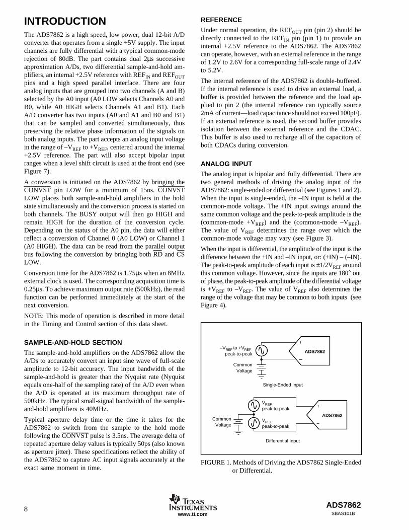
The analog input is bipolar and fully differential. There aretwo general methods of driving the analog input of theADS7862: single-ended or differential (see Figures 1 and 2).When the input is single-ended, the –IN input is held at thecommon-mode voltage. The +IN input swings around thesame common voltage and the peak-to-peak amplitude is the(common-mode +VREF) and the (common-mode –VREF).The value of VREF determines the range over which thecommon-mode voltage may vary (see Figure 3).
When the input is differential, the amplitude of the input is thedifference between the +IN and –IN input, or: (+IN) – (–IN).The peak-to-peak amplitude of each input is ±1/2VREF aroundthis common voltage. However, since the inputs are 180° outof phase, the peak-to-peak amplitude of the differential voltageis +VREF to –VREF. The value of VREF also determines therange of the voltage that may be common to both inputs (seeFigure 4).
INTRODUCTIONThe ADS7862 is a high speed, low power, dual 12-bit A/Dconverter that operates from a single +5V supply. The inputchannels are fully differential with a typical common-moderejection of 80dB. The part contains dual 2µs successiveapproximation A/Ds, two differential sample-and-hold am-plifiers, an internal +2.5V reference with REFIN and REFOUTpins and a high speed parallel interface. There are fouranalog inputs that are grouped into two channels (A and B)selected by the A0 input (A0 LOW selects Channels A0 andB0, while A0 HIGH selects Channels A1 and B1). EachA/D converter has two inputs (A0 and A1 and B0 and B1)that can be sampled and converted simultaneously, thuspreserving the relative phase information of the signals onboth analog inputs. The part accepts an analog input voltagein the range of –VREF to +VREF, centered around the internal+2.5V reference. The part will also accept bipolar inputranges when a level shift circuit is used at the front end (seeFigure 7).
A conversion is initiated on the ADS7862 by bringing theCONVST pin LOW for a minimum of 15ns. CONVSTLOW places both sample-and-hold amplifiers in the holdstate simultaneously and the conversion process is started onboth channels. The BUSY output will then go HIGH andremain HIGH for the duration of the conversion cycle.Depending on the status of the A0 pin, the data will eitherreflect a conversion of Channel 0 (A0 LOW) or Channel 1(A0 HIGH). The data can be read from the parallel outputbus following the conversion by bringing both RD and CSLOW.
Conversion time for the ADS7862 is 1.75µs when an 8MHzexternal clock is used. The corresponding acquisition time is0.25µs. To achieve maximum output rate (500kHz), the readfunction can be performed immediately at the start of thenext conversion.
NOTE: This mode of operation is described in more detailin the Timing and Control section of this data sheet.
SAMPLE-AND-HOLD SECTION
The sample-and-hold amplifiers on the ADS7862 allow theA/Ds to accurately convert an input sine wave of full-scaleamplitude to 12-bit accuracy. The input bandwidth of thesample-and-hold is greater than the Nyquist rate (Nyquistequals one-half of the sampling rate) of the A/D even whenthe A/D is operated at its maximum throughput rate of500kHz. The typical small-signal bandwidth of the sample-and-hold amplifiers is 40MHz.
Typical aperture delay time or the time it takes for theADS7862 to switch from the sample to the hold modefollowing the CONVST pulse is 3.5ns. The average delta ofrepeated aperture delay values is typically 50ps (also knownas aperture jitter). These specifications reflect the ability ofthe ADS7862 to capture AC input signals accurately at theexact same moment in time.
ADS7862
ADS7862
Single-Ended Input
CommonVoltage
–VREF to +VREF peak-to-peak
Differential Input
CommonVoltage
VREFpeak-to-peak
VREFpeak-to-peak
FIGURE 1. Methods of Driving the ADS7862 Single-Endedor Differential.

ADS7862 9SBAS101B www.ti.com
FIGURE 3. Single-Ended Input: Common-Mode VoltageRange vs VREF.
1.0 1.51.2
2.0 2.52.6
3.0
VREF (V)
Co
mm
on
Vo
ltag
e R
an
ge
(V
)
–1
0
1
2
3
4
5
2.7
2.3
4.1
0.9
VCC = 5V
Single-Ended Input Differential Input
1.0 1.51.2
2.0 2.52.6
3.0
VREF (V)
Com
mon V
olta
ge R
ange (
V)
–1
0
1
2
3
4
5
4.7
0.3
VCC = 5V
4.05
0.90
FIGURE 2. Using the ADS7862 in the Single-Ended and Differential Input Modes.
FIGURE 4. Differential Input: Common-Mode VoltageRange vs VREF.
In each case, care should be taken to ensure that the outputimpedance of the sources driving the +IN and –IN inputs arematched. Otherwise, this may result in offset error, whichwill change with both temperature and input voltage.
The input current on the analog inputs depend on a numberof factors: sample rate, input voltage, and source impedance.Essentially, the current into the ADS7862 charges the inter-nal capacitor array during the sampling period. After this
capacitance has been fully charged, there is no further inputcurrent. The source of the analog input voltage must be ableto charge the input capacitance (15pF) to a 12-bit settlinglevel within 2 clock cycles. When the converter goes into thehold mode, the input impedance is greater than 1GΩ.
Care must be taken regarding the absolute analog inputvoltage. The +IN input should always remain within therange of GND – 300mV to VDD + 0.3V.
CM +VREF
+VREF
–VREF
Single-Ended Inputst
+IN
CM Voltage
CM –VREF
CM +1/2VREF
Differential Inputs
NOTES: Common-Mode Voltage (Differential Mode) = Common-Mode Voltage (Single-Ended Mode) = IN–.(IN+) + (IN–)
2The maximum differential voltage between +IN and –IN of the ADS7862 is VREF. See Figures 3 and 4 for a furtherexplanation of the common voltage range for single-ended and differential inputs.
t
+IN
–IN
CM Voltage
CM –1/2VREF
–IN = CM Voltage
+VREF
–VREF

ADS786210SBAS101Bwww.ti.com
Three timing diagrams are used to explain the operation ofthe ADS7862. Figure 8 shows the timing relationship be-tween the CLOCK, CONVST (pin 18) and the conversion
Code (decimal)
8000
7000
6000
5000
4000
3000
2000
1000
0
Num
ber
of C
onve
rsio
ns
2044 2045 2046 2047 2048
FIGURE 5. Histogram of 8,000 Conversions of a DC Input.
FIGURE 6. Test Circuits for Timing Specifications.
FIGURE 7. Level Shift Circuit for Bipolar Input Ranges.
FIGURE 8. Conversion Mode.
TRANSITION NOISE
Figure 5 shows a histogram plot for the ADS7862 following8,000 conversions of a DC input. The DC input was set atoutput code 2046. All but one of the conversions had anoutput code result of 2046 (one of the conversions resultedin an output of 2047). The histogram reveals the excellentnoise performance of the ADS7862.
BIPOLAR INPUTS
The differential inputs of the ADS7862 were designed toaccept bipolar inputs (–VREF and +VREF) around the internalreference voltage (2.5V), which corresponds to a 0V to 5Vinput range with a 2.5V reference. By using a simple op ampcircuit featuring a single amplifier and four external resis-tors, the ADS7862 can be configured to except bipolarinputs. The conventional ±2.5V, ±5V, and ±10V inputranges can be interfaced to the ADS7862 using the resistorvalues shown in Figure 7.
TIMING AND CONTROL
The ADS7862 uses an external clock (CLOCK, pin 19)which controls the conversion rate of the CDAC. With an8MHz external clock, the A/D sampling rate is 500kHzwhich corresponds to a 2µs maximum throughput time.
DATA
1.4V
Test Point
3kΩ
100pFCLOAD
tR
DATA
Voltage Waveforms for DATA Rise and Fall Times tR, and tF.
VOH
VOL
tF
R1
R2
+IN
–IN
REFOUT (pin 2)2.5V
4kΩ
20kΩBipolar Input
BIPOLAR INPUT R1 R2
±10V 1kΩ 5kΩ±5V 2kΩ 10kΩ
±2.5V 4kΩ 20kΩ
OPA132
ADS7862
CONVST
CONVERSIONMODE
SAMPLE HOLD CONVERT
CLOCK
tCKH
tCKP
t3
tCKL
NOTE: The ADS7862 will switch from the sample to the hold mode the instant CONVST goes LOW regardless of the state of the external clock. The conversion process is initiated with the first rising edge of the external clock following CONVST going LOW.

ADS7862 11SBAS101B www.ti.com
FIGURE 9. Reading and Writing to the ADS7862 During the Same Cycle.
DESCRIPTION ANALOG INPUT
Full-Scale Input Span –VREF to +VREF(1)
Least Significant (–VREF to +VREF)/4096(2)
Bit (LSB)
+Full Scale 4.99878V 0111 1111 1111 7FF
Midscale 2.5V 0000 0000 0000 000
Midscale – 1 LSB 2.49878V 1111 1111 1111 FFF
–Full Scale 0V 1000 0000 0000 800
NOTES: (1) –VREF to +VREF around VREF. With a 2.5V reference, this corre-sponds to a 0V to 5V input span. (2) 1.22mV with a 2.5V reference.
TABLE I. Ideal Input Voltages and Output Codes.
DIGITAL OUTPUTBINARY TWO’S COMPLEMENT
BINARY CODE HEX CODE
mode. Figure 9, in conjunction with Table I, shows the basicread/write functions of the ADS7862 and highlights all ofthe timing specifications. Figure 10 shows a more detaileddescription of initiating a conversion using CONVST. Fig-ure 11 illustrates three consecutive conversions and, with theaccompanying text, describes all of the read and writecapabilities of the ADS7862.
The Figure 11 timing diagram can be divided into threesections: (a) initiating a conversion (n – 2), (b) starting asecond conversion (n – 1) while reading the data output fromthe previous conversion (n – 2), and (c) starting a thirdconversion (n) while reading both previous conversions(n – 2 and n – 1). In this sequence, Channel 0 is converted
SYMBOL DESCRIPTION MIN TYP MAX UNITS
tCONV Conversion Time 1.75 µstACQ Acquisition Time 0.25 µstCKP Clock Period 125 5000 nstCKL Clock LOW 40 nstCKH Clock HIGH 40 nst1 CS to RD Setup Time 0 nst2 CS to RD Hold Time 0 nst3 CONVST LOW 15 nst4 RD Pulse Width 30 nst5 RD to Valid Data (Bus Access) 16 25 nst6 RD to HI-Z Delay (Bus Relinquish) 10 20 nst7 Time Between Conversion Reads 40 nst8 Address Setup Time 250 nst9 CONVST HIGH 20 nst10 Address Hold Time 20 nst11 CONVST to BUSY Propagation Delay 30 nst12 CONVST LOW Prior to CLOCK Rising Edge 10 nst13 CONVST LOW After CLOCK Rising Edge 5 nstF Data Fall Time 13 25 nstR Data Rise Time 20 30 ns
TIMING SPECIFICATIONS
first followed by Channel 1. Channel 1 can be convertedprior to Channel 0 if the user wishes by simply starting theconversion process with the A0 pin at logic HIGH (Channel1) followed by logic LOW (Channel 0).
t12 t13
t3 t9
t11 Conversion n
Conversion n – 1 Results Conversion n Results
BUSY
A0
CS
RD
DATA
Conversion n + 1
1CLOCK
CONVST
2 3 4 5 14 15 16 1 2 3 4 5 14 15 16
tCONV tACQ
t8
t4
t10
t1
t5
CHA1 CHB1 CHA0 CHB0
t6
t2t7

ADS786212SBAS101Bwww.ti.com
NOTE: All CONVST commands which occur more than 10ns before the rising edge of cycle ‘1’ of the external clock (Region ‘A’) will initiate a conversion on the rising edge of cycle ‘1’. All CONVST commands which occur 5ns after the rising edge of cycle ‘1’ or 10ns before the rising edge of cycle 2 (Region ‘B’) will initiate a conversion on the rising edge of cycle ‘2’. All CONVST commands which occur 5ns after the rising edge of cycle ‘2’ (Region ‘C’) will initiate a conversion on the rising edge of the next clock period. The CONVST pin should never be switched from HIGH to LOW in the region 10ns prior to the rising edge of the CLOCK and 5ns after the rising edge (gray areas). If CONVST is toggled in this gray area, the conversion could begin on either the same rising edge of the CLOCK or the following edge.
CLOCK
CONVST
Cycle 1 Cycle 2
tCKP125ns
10ns
5ns
10ns
5ns
A B C
FIGURE 10. Timing Between CLOCK and CONVST to Start a Conversion.
FIGURE 11. ADS7862 Timing Diagram Showing Complete Functionality.
1 11
SECTION A
CLOCK
CONVST
A0
RD
CS
DATA
BUSY
TIME 0 1µ 2µ 3µ 4µ 5µ
min 250ns
SECTION B SECTION C
ChA0 ChB0
Time (seconds)
ChA1 ChA0
4 Output-Register
Data of Ch0 Still Stored
A0 Selects BetweenCh0 and Ch1 at Output
Conversion of Ch0
Low Data Level Tri-state of Output
Conversion of Ch0
High Data Level Output Active
1616
A0 = 1 Conversion of Ch1
min 250ns
CS Needed Only During Reading
Conversion of Ch1
ChB0ChB1
A0 = 0 Conversion of Ch0A0 = 0 Conversion of Ch0
1st RD After CONVST ChA at Output 2nd RD After CONVST ChB at Output

ADS7862 13SBAS101B www.ti.com
SECTION A
Conversions are initiated by bringing the CONVST pin (pin18) LOW for a minimum of 5ns (after the 5ns minimumrequirement has been met, the CONVST pin can be broughtHIGH). The ADS7862 will switch from the sample to thehold mode on the falling edge of the CONVST command.Following the first rising edge of the external clock after aCONVST LOW, the ADS7862 will begin conversion (thisfirst rising edge of the external clock represents the start ofclock cycle one; the ADS7862 requires sixteen cycles tocomplete a conversion). The input channel is also latched inat this point in time. The A0 input (pin 22) must be selected250ns prior to the CONVST pin going LOW so that thecorrect address will be selected prior to conversion. TheBUSY output will go HIGH immediately following CONVSTgoing LOW. BUSY will stay HIGH through the conversionprocess and return LOW when the conversion has ended.After CONVST has remained LOW for the minimum time,the ADS7862 will switch from the hold mode to the conver-sion mode synchronous to the next rising edge of theexternal clock and conversion ‘n – 2’ will begin. Both RD(pin 21) and CS (pin 20) can be HIGH during and before aconversion. However, they must both be LOW to enable theoutput bus and read data out.
SECTION B
The CONVST pin is switched from HIGH to LOW a secondtime to initiate conversion ‘n – 1’. Again, the address must beselected 250ns prior to CONVST going LOW to ensure thatthe new address is selected for conversion. Both the RD andCS pins are brought LOW in order to enable the parallel outputbus with the ‘n – 2’ conversion results of Channel A0. Whilecontinuing to hold CS LOW, RD is held LOW for a minimumof 30ns which enables the output bus with the Channel A0results of conversion ‘n – 2’. The RD pin is toggled fromHIGH to LOW a second time in order to enable the output buswith the Channel B0 results of conversion ‘n – 2’.
SECTION C
CONVST is brought LOW for a third time to initiateconversion ‘n’ (Channel 0). While the conversion is inprocess, the results for both conversions ‘n – 2’ and ‘n – 1’can be read. The address pin is brought HIGH while CS andRD are brought LOW which enables the output bus with theChannel A1 results of conversion ‘n – 1’. The RD pin istoggled from HIGH to LOW for a second time in Section Cand the ‘n – 1’ conversion results for Channel B1 appear atthe output bus. The address pin (A0) is then brought LOWand the read process repeats itself with the most recentconversion results for Channel 0 (n – 2) appearing at theoutput bus.
READING DATA
The ADS7862 outputs full parallel data in Binary Two’sComplement data output format. The parallel output will beactive when CS (pin 20) and RD (pin 21) are both LOW. The
output data should not be read 125ns prior to the falling edgeof CONVST and 10ns after the falling edge. Any othercombination of CS and RD will tri-state the parallel output.Valid conversion data can be read on pins 5 through 16(MSB–LSB). Refer to Table I for ideal output codes.
In applications where multiple devices are present on thedata bus, care should be taken to ensure that the signalapplied to RD (pin 21) is toggled only when the target deviceis properly chip-selected. Toggling the RD pin will advancethe internal read pointer regardless of the state of the chipselect, causing the output data to appear channel-swapped.If multiple devices share a single read enable from the hostprocessor, the signal may be ORed with an address-decodedchip select to ensure channel data integrity. For more infor-mation, refer to Application Report SBAA138, ReadingData from the ADS7862, available for download from the TIwebsite at www.ti.com.
LAYOUTFor optimum performance, care should be taken with thephysical layout of the ADS7862 circuitry. This is particu-larly true if the CLOCK input is approaching the maximumthroughput rate.
The basic SAR architecture is sensitive to glitches or suddenchanges on the power supply, reference, ground connectionsand digital inputs that occur just prior to latching the outputof the analog comparator. Thus, driving any single conver-sion for an n-bit SAR converter, there are n “windows” inwhich large external transient voltages can affect the conver-sion result. Such glitches might originate from switchingpower supplies, nearby digital logic or high power devices.The degree of error in the digital output depends on thereference voltage, layout, and the exact timing of the exter-nal event. This error can change if the external event changesin time with respect to the CLOCK input.
With this in mind, power to the ADS7862 should be cleanand well bypassed. A 0.1µF ceramic bypass capacitor shouldbe placed as close to the device as possible. In addition, a1µF to 10µF capacitor is recommended. If needed, an evenlarger capacitor and a 5Ω or 10Ω series resistor may be usedto low-pass filter a noisy supply. On average, the ADS7862draws very little current from an external reference as thereference voltage is internally buffered. If the referencevoltage is external and originates from an op amp, make surethat it can drive the bypass capacitor or capacitors withoutoscillation. A bypass capacitor is not necessary when usingthe internal reference (tie pin 1 directly to pin 2).
The AGND and DGND pins should be connected to a cleanground point. In all cases, this should be the ‘analog’ground. Avoid connections which are too close to the ground-ing point of a microcontroller or digital signal processor. Ifrequired, run a ground trace directly from the converter tothe power supply entry point. The ideal layout will includean analog ground plane dedicated to the converter andassociated analog circuitry.

PACKAGE OPTION ADDENDUM
www.ti.com 12-Jul-2016
Addendum-Page 1
PACKAGING INFORMATION
Orderable Device Status(1)
Package Type PackageDrawing
Pins PackageQty
Eco Plan(2)
Lead/Ball Finish(6)
MSL Peak Temp(3)
Op Temp (°C) Device Marking(4/5)
Samples
ADS7862Y/250 ACTIVE TQFP PBS 32 250 Green (RoHS& no Sb/Br)
CU NIPDAU Level-3-260C-168 HR -40 to 85 7862Y
ADS7862Y/250G4 ACTIVE TQFP PBS 32 250 Green (RoHS& no Sb/Br)
CU NIPDAU Level-3-260C-168 HR -40 to 85 7862Y
ADS7862Y/2K ACTIVE TQFP PBS 32 2000 Green (RoHS& no Sb/Br)
CU NIPDAU Level-3-260C-168 HR 7862Y
ADS7862Y/2KG4 ACTIVE TQFP PBS 32 2000 Green (RoHS& no Sb/Br)
CU NIPDAU Level-3-260C-168 HR 7862Y
ADS7862YB/250 ACTIVE TQFP PBS 32 250 Green (RoHS& no Sb/Br)
CU NIPDAU Level-3-260C-168 HR 7862YB
ADS7862YB/250G4 ACTIVE TQFP PBS 32 250 Green (RoHS& no Sb/Br)
CU NIPDAU Level-3-260C-168 HR 7862YB
(1) The marketing status values are defined as follows:ACTIVE: Product device recommended for new designs.LIFEBUY: TI has announced that the device will be discontinued, and a lifetime-buy period is in effect.NRND: Not recommended for new designs. Device is in production to support existing customers, but TI does not recommend using this part in a new design.PREVIEW: Device has been announced but is not in production. Samples may or may not be available.OBSOLETE: TI has discontinued the production of the device.
(2) Eco Plan - The planned eco-friendly classification: Pb-Free (RoHS), Pb-Free (RoHS Exempt), or Green (RoHS & no Sb/Br) - please check http://www.ti.com/productcontent for the latest availabilityinformation and additional product content details.TBD: The Pb-Free/Green conversion plan has not been defined.Pb-Free (RoHS): TI's terms "Lead-Free" or "Pb-Free" mean semiconductor products that are compatible with the current RoHS requirements for all 6 substances, including the requirement thatlead not exceed 0.1% by weight in homogeneous materials. Where designed to be soldered at high temperatures, TI Pb-Free products are suitable for use in specified lead-free processes.Pb-Free (RoHS Exempt): This component has a RoHS exemption for either 1) lead-based flip-chip solder bumps used between the die and package, or 2) lead-based die adhesive used betweenthe die and leadframe. The component is otherwise considered Pb-Free (RoHS compatible) as defined above.Green (RoHS & no Sb/Br): TI defines "Green" to mean Pb-Free (RoHS compatible), and free of Bromine (Br) and Antimony (Sb) based flame retardants (Br or Sb do not exceed 0.1% by weightin homogeneous material)
(3) MSL, Peak Temp. - The Moisture Sensitivity Level rating according to the JEDEC industry standard classifications, and peak solder temperature.
(4) There may be additional marking, which relates to the logo, the lot trace code information, or the environmental category on the device.
(5) Multiple Device Markings will be inside parentheses. Only one Device Marking contained in parentheses and separated by a "~" will appear on a device. If a line is indented then it is a continuationof the previous line and the two combined represent the entire Device Marking for that device.

PACKAGE OPTION ADDENDUM
www.ti.com 12-Jul-2016
Addendum-Page 2
(6) Lead/Ball Finish - Orderable Devices may have multiple material finish options. Finish options are separated by a vertical ruled line. Lead/Ball Finish values may wrap to two lines if the finishvalue exceeds the maximum column width.
Important Information and Disclaimer:The information provided on this page represents TI's knowledge and belief as of the date that it is provided. TI bases its knowledge and belief on informationprovided by third parties, and makes no representation or warranty as to the accuracy of such information. Efforts are underway to better integrate information from third parties. TI has taken andcontinues to take reasonable steps to provide representative and accurate information but may not have conducted destructive testing or chemical analysis on incoming materials and chemicals.TI and TI suppliers consider certain information to be proprietary, and thus CAS numbers and other limited information may not be available for release.
In no event shall TI's liability arising out of such information exceed the total purchase price of the TI part(s) at issue in this document sold by TI to Customer on an annual basis.

TAPE AND REEL INFORMATION
*All dimensions are nominal
Device PackageType
PackageDrawing
Pins SPQ ReelDiameter
(mm)
ReelWidth
W1 (mm)
A0(mm)
B0(mm)
K0(mm)
P1(mm)
W(mm)
Pin1Quadrant
ADS7862Y/250 TQFP PBS 32 250 180.0 16.4 7.2 7.2 1.5 12.0 16.0 Q2
ADS7862Y/2K TQFP PBS 32 2000 330.0 16.4 7.2 7.2 1.5 12.0 16.0 Q2
ADS7862YB/250 TQFP PBS 32 250 180.0 16.4 7.2 7.2 1.5 12.0 16.0 Q2
PACKAGE MATERIALS INFORMATION
www.ti.com 7-Feb-2015
Pack Materials-Page 1

*All dimensions are nominal
Device Package Type Package Drawing Pins SPQ Length (mm) Width (mm) Height (mm)
ADS7862Y/250 TQFP PBS 32 250 213.0 191.0 55.0
ADS7862Y/2K TQFP PBS 32 2000 367.0 367.0 38.0
ADS7862YB/250 TQFP PBS 32 250 213.0 191.0 55.0
PACKAGE MATERIALS INFORMATION
www.ti.com 7-Feb-2015
Pack Materials-Page 2


IMPORTANT NOTICE
Texas Instruments Incorporated and its subsidiaries (TI) reserve the right to make corrections, enhancements, improvements and otherchanges to its semiconductor products and services per JESD46, latest issue, and to discontinue any product or service per JESD48, latestissue. Buyers should obtain the latest relevant information before placing orders and should verify that such information is current andcomplete. All semiconductor products (also referred to herein as “components”) are sold subject to TI’s terms and conditions of salesupplied at the time of order acknowledgment.TI warrants performance of its components to the specifications applicable at the time of sale, in accordance with the warranty in TI’s termsand conditions of sale of semiconductor products. Testing and other quality control techniques are used to the extent TI deems necessaryto support this warranty. Except where mandated by applicable law, testing of all parameters of each component is not necessarilyperformed.TI assumes no liability for applications assistance or the design of Buyers’ products. Buyers are responsible for their products andapplications using TI components. To minimize the risks associated with Buyers’ products and applications, Buyers should provideadequate design and operating safeguards.TI does not warrant or represent that any license, either express or implied, is granted under any patent right, copyright, mask work right, orother intellectual property right relating to any combination, machine, or process in which TI components or services are used. Informationpublished by TI regarding third-party products or services does not constitute a license to use such products or services or a warranty orendorsement thereof. Use of such information may require a license from a third party under the patents or other intellectual property of thethird party, or a license from TI under the patents or other intellectual property of TI.Reproduction of significant portions of TI information in TI data books or data sheets is permissible only if reproduction is without alterationand is accompanied by all associated warranties, conditions, limitations, and notices. TI is not responsible or liable for such altereddocumentation. Information of third parties may be subject to additional restrictions.Resale of TI components or services with statements different from or beyond the parameters stated by TI for that component or servicevoids all express and any implied warranties for the associated TI component or service and is an unfair and deceptive business practice.TI is not responsible or liable for any such statements.Buyer acknowledges and agrees that it is solely responsible for compliance with all legal, regulatory and safety-related requirementsconcerning its products, and any use of TI components in its applications, notwithstanding any applications-related information or supportthat may be provided by TI. Buyer represents and agrees that it has all the necessary expertise to create and implement safeguards whichanticipate dangerous consequences of failures, monitor failures and their consequences, lessen the likelihood of failures that might causeharm and take appropriate remedial actions. Buyer will fully indemnify TI and its representatives against any damages arising out of the useof any TI components in safety-critical applications.In some cases, TI components may be promoted specifically to facilitate safety-related applications. With such components, TI’s goal is tohelp enable customers to design and create their own end-product solutions that meet applicable functional safety standards andrequirements. Nonetheless, such components are subject to these terms.No TI components are authorized for use in FDA Class III (or similar life-critical medical equipment) unless authorized officers of the partieshave executed a special agreement specifically governing such use.Only those TI components which TI has specifically designated as military grade or “enhanced plastic” are designed and intended for use inmilitary/aerospace applications or environments. Buyer acknowledges and agrees that any military or aerospace use of TI componentswhich have not been so designated is solely at the Buyer's risk, and that Buyer is solely responsible for compliance with all legal andregulatory requirements in connection with such use.TI has specifically designated certain components as meeting ISO/TS16949 requirements, mainly for automotive use. In any case of use ofnon-designated products, TI will not be responsible for any failure to meet ISO/TS16949.
Products ApplicationsAudio www.ti.com/audio Automotive and Transportation www.ti.com/automotiveAmplifiers amplifier.ti.com Communications and Telecom www.ti.com/communicationsData Converters dataconverter.ti.com Computers and Peripherals www.ti.com/computersDLP® Products www.dlp.com Consumer Electronics www.ti.com/consumer-appsDSP dsp.ti.com Energy and Lighting www.ti.com/energyClocks and Timers www.ti.com/clocks Industrial www.ti.com/industrialInterface interface.ti.com Medical www.ti.com/medicalLogic logic.ti.com Security www.ti.com/securityPower Mgmt power.ti.com Space, Avionics and Defense www.ti.com/space-avionics-defenseMicrocontrollers microcontroller.ti.com Video and Imaging www.ti.com/videoRFID www.ti-rfid.comOMAP Applications Processors www.ti.com/omap TI E2E Community e2e.ti.comWireless Connectivity www.ti.com/wirelessconnectivity
Mailing Address: Texas Instruments, Post Office Box 655303, Dallas, Texas 75265Copyright © 2016, Texas Instruments Incorporated