ads890xb 20-bit, high-speed sar adcs with … rst 2 17 sdo-3 22 sdi 9 ainp refin 3 16 dvdd 21 rvs 10...
TRANSCRIPT

SPIADC
BUFREFIN
REFBUFOUT
DECAP
DVDD
ADS890xB
AINP
AINMRVDD
SPIADC
BUFREFIN
REFBUFOUT
DVDD
ADS890xB
AINP
AINMRVDD
Data
ADC
REFINREFBUFOUT
DVDD
ADS89xxB
AINP
AINM
AVDD
AVDD
VREF
AINM
ADS89xxB
AINP
AINM
CS
SCLK
SDO
CONV
CS
SDI
SCK22-MHz
Multi-ADC System with Single Supply and Reference
Lowest Clock Speeds at 1-MSPS using 3-Wire Enhanced-SPI
MCU
ISO
ADC ConversionData Read
ADC Conversion
Enhanced SPI (Data + Parity)SPI
22-MHz70-MHz
Parity
Quiet time
Data
ParityBUF
Product
Folder
Order
Now
Technical
Documents
Tools &
Software
Support &Community
An IMPORTANT NOTICE at the end of this data sheet addresses availability, warranty, changes, use in safety-critical applications,intellectual property matters and other important disclaimers. PRODUCTION DATA.
ADS8900B, ADS8902B, ADS8904BSBAS728A –NOVEMBER 2016–REVISED JUNE 2017
ADS890xB 20-Bit, High-Speed SAR ADCs With Integrated Reference Buffer, andEnhanced Performance Features
1
1 Features1• Resolution: 20-Bits• High Sample Rate With No Latency Output:
– ADS8900B: 1-MSPS– ADS8902B: 500-kSPS– ADS8904B: 250-kSPS
• Integrated LDO Enables Low-Power, Single-Supply Operation
• Low Power Reference Buffer with No Droop• Excellent AC and DC Performance:
– SNR: 104.5-dB, THD: –125-dB– DNL: ±0.2-ppm, 20-Bit No-Missing-Codes– INL: ±1-ppm
• Wide Input Range:– Unipolar Differential Input Range: ±VREF
– VREF Input Range: 2.5-V to 5-V• Enhanced-SPI Digital Interface
– Interface SCLK : 22-MHz at 1-MSPS.– Configurable Data Parity Output.
• Extended Temperature Range: –40°C to +125°C• Small Footprint: 4-mm × 4-mm VQFN
2 Applications• Test and Measurement• Medical Imaging• High-Precision, High-Speed Data Acquisition
3 DescriptionThe ADS8900B, ADS8902B, and ADS8904B(ADS890xB) belong to a family of pin-to-pincompatible, high-speed, single-channel, high-precision, 20-bit successive-approximation-register(SAR) analog-to-digital converters (ADCs) with anintegrated reference buffer and integrated low-dropout regulator (LDO). The device family includesthe ADS891xB (18-bit) and ADS892xB (16-bit)resolution variants.
The ADS89xxB boosts analog performance whilemaintaining high-resolution data transfer by using TI’sEnhanced-SPI feature. Enhanced-SPI enablesADS89xxB in achieving high throughput at lowerclock speeds, there by simplifying the board layoutand lowering system cost. Enhanced-SPI alsosimplifies the host’s clocking-in of data there bymaking it ideal for applications involving FPGAs,DSPs. ADS89xxB is compatible with standard SPIInterface.
The ADS89xxB has an internal data parity featurewhich can be appended to the ADC data output. ADCdata validation by the host, using parity bits, improvessystem reliability.
SPI Interface Clock at 1 MSPSDEVICE
RESOLUTION 3-WIRE SPI 3-WIREENHANCED SPI
20 bits 70 MHz 22 MHz18 bits 58 MHz 20 MHz16 bits 52 MHz 18 MHz
(1) For all features of the enhanced SPI, see the InterfaceModule section.
Ease of System Design with ADS89xxB Integrated Features

2
ADS8900B, ADS8902B, ADS8904BSBAS728A –NOVEMBER 2016–REVISED JUNE 2017 www.ti.com
Product Folder Links: ADS8900B ADS8902B ADS8904B
Submit Documentation Feedback Copyright © 2016–2017, Texas Instruments Incorporated
Table of Contents1 Features .................................................................. 12 Applications ........................................................... 13 Description ............................................................. 14 Revision History..................................................... 25 Pin Configuration and Functions ......................... 36 Specifications......................................................... 5
6.1 Absolute Maximum Ratings ..................................... 56.2 ESD Ratings.............................................................. 56.3 Recommended Operating Conditions....................... 56.4 Thermal Information .................................................. 56.5 Electrical Characteristics........................................... 66.6 Timing Requirements ................................................ 86.7 Switching Characteristics .......................................... 96.8 Typical Characteristics ............................................ 13
7 Detailed Description ............................................ 187.1 Overview ................................................................. 187.2 Functional Block Diagram ....................................... 187.3 Feature Description................................................. 197.4 Device Functional Modes........................................ 25
7.5 Programming........................................................... 277.6 Register Maps ......................................................... 51
8 Application and Implementation ........................ 578.1 Application Information............................................ 578.2 Typical Application .................................................. 59
9 Power-Supply Recommendations...................... 6410 Layout................................................................... 65
10.1 Layout Guidelines ................................................. 6510.2 Layout Example .................................................... 66
11 Device and Documentation Support ................. 6711.1 Documentation Support ........................................ 6711.2 Related Links ........................................................ 6711.3 Receiving Notification of Documentation Updates 6711.4 Community Resources.......................................... 6711.5 Trademarks ........................................................... 6811.6 Electrostatic Discharge Caution............................ 6811.7 Glossary ................................................................ 68
12 Mechanical, Packaging, and OrderableInformation ........................................................... 68
4 Revision HistoryNOTE: Page numbers for previous revisions may differ from page numbers in the current version.
Changes from Original (November 2016) to Revision A Page
• Changed SPI Interface Clock at 1 MSPS table...................................................................................................................... 1• Changed DVDD specified throughput value in the Recommended Operating Conditions from 3.6 V to 5.5 V....................... 5• Changed maximum value for DVDD range in Electrical Characteristics, Timing Requirements, and Switching
Characteristics from 3.6 V to 5.5 V......................................................................................................................................... 6• Added TA = 25°C to reference buffer offset voltage test condition in Electrical Characteristics table ................................... 6• Changed input offset thermal drift typ value from 10 to 1 ...................................................................................................... 6• Added fIN = 2 kHz test condition to SFDR in Electrical Characteristics table ........................................................................ 7• Changed DAQ Circuit With FDA Input Driver and Single-Ended or Differential Input section for clarity ............................. 61
24C
S7
RE
FB
UF
OU
T
1CONVST 18 SDO-2
23S
CLK
8R
EF
M
2RST 17 SDO-3
22S
DI
9A
INP
3REFIN 16 DVDD
21R
VS
10A
INM
4REFM 15 GND
20S
DO
-011
GN
D
5REFBUFOUT 14 DECAP
19S
DO
-112
RV
DD
6NC 13 DECAP
Not to scale
Thermal
Pad
3
ADS8900B, ADS8902B, ADS8904Bwww.ti.com SBAS728A –NOVEMBER 2016–REVISED JUNE 2017
Product Folder Links: ADS8900B ADS8902B ADS8904B
Submit Documentation FeedbackCopyright © 2016–2017, Texas Instruments Incorporated
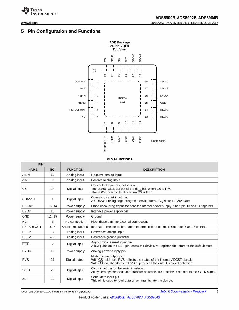
5 Pin Configuration and Functions
RGE Package24-Pin VQFN
Top View
Pin FunctionsPIN
FUNCTION DESCRIPTIONNAME NO.AINM 10 Analog input Negative analog inputAINP 9 Analog input Positive analog input
CS 24 Digital inputChip-select input pin; active lowThe device takes control of the data bus when CS is low.The SDO-x pins go to Hi-Z when CS is high.
CONVST 1 Digital input Conversion start input pin.A CONVST rising edge brings the device from ACQ state to CNV state.
DECAP 13, 14 Power supply Place decoupling capacitor here for internal power supply. Short pin 13 and 14 together.DVDD 16 Power supply Interface power supply pinGND 11, 15 Power supply GroundNC 6 No connection Float these pins; no external connection.REFBUFOUT 5, 7 Analog input/output Internal reference buffer output, external reference input. Short pin 5 and 7 together.REFIN 3 Analog input Reference voltage inputREFM 4, 8 Analog input Reference ground potential
RST 2 Digital input Asynchronous reset input pin.A low pulse on the RST pin resets the device. All register bits return to the default state.
RVDD 12 Power supply Analog power supply pin.
RVS 21 Digital outputMultifunction output pin.With CS held high, RVS reflects the status of the internal ADCST signal.With CS low, the status of RVS depends on the output protocol selection.
SCLK 23 Digital input Clock input pin for the serial interface.All system-synchronous data transfer protocols are timed with respect to the SCLK signal.
SDI 22 Digital input Serial data input pin.This pin is used to feed data or commands into the device.

4
ADS8900B, ADS8902B, ADS8904BSBAS728A –NOVEMBER 2016–REVISED JUNE 2017 www.ti.com
Product Folder Links: ADS8900B ADS8902B ADS8904B
Submit Documentation Feedback Copyright © 2016–2017, Texas Instruments Incorporated
Pin Functions (continued)PIN
FUNCTION DESCRIPTIONNAME NO.SDO-0 20 Digital output Serial communication pin: data output 0SDO-1 19 Digital output Serial communication pin: data output 1SDO-2 18 Digital output Serial communication pin: data output 2SDO-3 17 Digital output Serial communication pin: data output 3Thermal pad Supply Exposed thermal pad; connect to GND.
5
ADS8900B, ADS8902B, ADS8904Bwww.ti.com SBAS728A –NOVEMBER 2016–REVISED JUNE 2017
Product Folder Links: ADS8900B ADS8902B ADS8904B
Submit Documentation FeedbackCopyright © 2016–2017, Texas Instruments Incorporated
(1) Stresses beyond those listed under Absolute Maximum Ratings may cause permanent damage to the device. These are stress ratingsonly, which do not imply functional operation of the device at these or any other conditions beyond those indicated under RecommendedOperating Conditions. Exposure to absolute-maximum-rated conditions for extended periods may affect device reliability.
6 Specifications
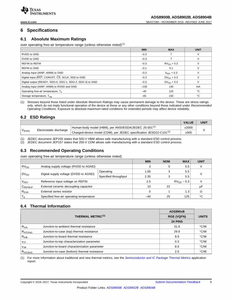
6.1 Absolute Maximum Ratingsover operating free-air temperature range (unless otherwise noted) (1)
MIN MAX UNIT
RVDD to GND –0.3 7 V
DVDD to GND –0.3 7 V
REFIN to REFM –0.3 RVDD + 0.3 V
REFM to GND –0.1 0.1 V
Analog Input (AINP, AINM) to GND –0.3 VREF + 0.3 V
Digital input (RST, CONVST, CS, SCLK, SDI) to GND –0.3 DVDD + 0.3 V
Digital output (READY, SDO-0, SDO-1, SDO-2, SDO-3) to GND –0.3 DVDD + 0.3 V
Analog Input (AINP, AINM) to RVDD and GND –130 130 mA
Operating free-air temperature, TA –40 125 °C
Storage temperature, Tstg –65 150 °C
(1) JEDEC document JEP155 states that 500-V HBM allows safe manufacturing with a standard ESD control process.(2) JEDEC document JEP157 states that 250-V CDM allows safe manufacturing with a standard ESD control process.
6.2 ESD RatingsVALUE UNIT
V(ESD) Electrostatic dischargeHuman-body model (HBM), per ANSI/ESDA/JEDEC JS-001 (1) ±2000
VCharged-device model (CDM), per JEDEC specification JESD22-C101 (2) ±500
6.3 Recommended Operating Conditionsover operating free-air temperature range (unless otherwise noted)
MIN NOM MAX UNITRVDD Analog supply voltage (RVDD to AGND) 3 5 5.5 V
DVDD Digital supply voltage (DVDD to AGND)Operating 1.65 3 5.5
VSpecified throughput 2.35 3 5.5
VREF Reference input voltage on REFIN 2.5 RVDD – 0.3 VCREFBUF External ceramic decoupling capacitor 10 22 µFRESR External series resistor 0 1 1.3 Ω
TA Specified free-air operating temperature –40 25 125 °C
(1) For more information about traditional and new thermal metrics, see the Semiconductor and IC Package Thermal Metrics applicationreport.
6.4 Thermal Information
THERMAL METRIC (1)ADS890xB
UNITSRGE (VQFN)24 PINS
RθJA Junction-to-ambient thermal resistance 31.9 °C/WRθJC(top) Junction-to-case (top) thermal resistance 29.9 °C/WRθJB Junction-to-board thermal resistance 8.9 °C/WψJT Junction-to-top characterization parameter 0.3 °C/WψJB Junction-to-board characterization parameter 8.9 °C/WRθJC(bot) Junction-to-case (bottom) thermal resistance 2.0 °C/W
6
ADS8900B, ADS8902B, ADS8904BSBAS728A –NOVEMBER 2016–REVISED JUNE 2017 www.ti.com
Product Folder Links: ADS8900B ADS8902B ADS8904B
Submit Documentation Feedback Copyright © 2016–2017, Texas Instruments Incorporated
(1) See the REF_MRG Register.(2) For selected VREF, see the OFST_CAL Register.(3) While operating with internal reference buffer and LDO.(4) See for statistical distribution data for DNL, INL, offset, and gain error parameters.(5) LSB = least-significant bit. 1 LSB at 20-bit resolution is approximately 0.95 ppm.(6) Includes internal reference buffer errors and drifts.
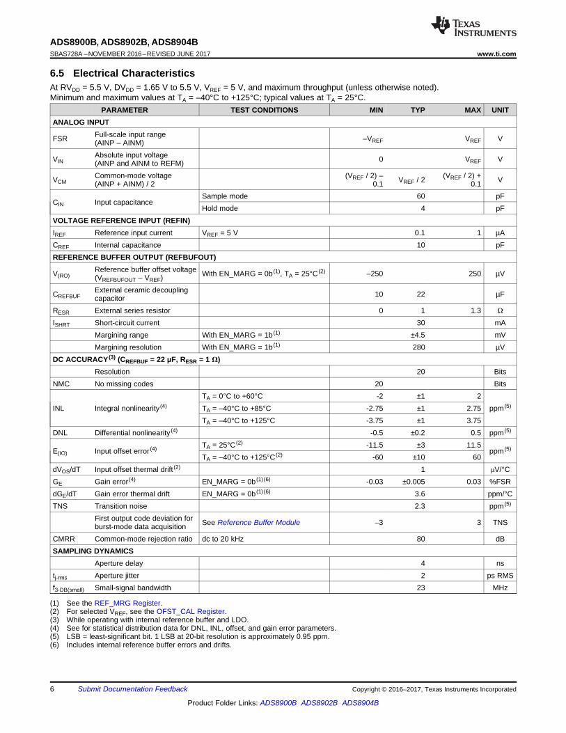
6.5 Electrical CharacteristicsAt RVDD = 5.5 V, DVDD = 1.65 V to 5.5 V, VREF = 5 V, and maximum throughput (unless otherwise noted).Minimum and maximum values at TA = –40°C to +125°C; typical values at TA = 25°C.
PARAMETER TEST CONDITIONS MIN TYP MAX UNITANALOG INPUT
FSR Full-scale input range(AINP – AINM) –VREF VREF V
VINAbsolute input voltage(AINP and AINM to REFM) 0 VREF V
VCMCommon-mode voltage(AINP + AINM) / 2
(VREF / 2) –0.1 VREF / 2 (VREF / 2) +
0.1 V
CIN Input capacitanceSample mode 60 pFHold mode 4 pF
VOLTAGE REFERENCE INPUT (REFIN)IREF Reference input current VREF = 5 V 0.1 1 µACREF Internal capacitance 10 pFREFERENCE BUFFER OUTPUT (REFBUFOUT)
V(RO)Reference buffer offset voltage(VREFBUFOUT – VREF) With EN_MARG = 0b (1), TA = 25°C (2) –250 250 µV
CREFBUFExternal ceramic decouplingcapacitor 10 22 µF
RESR External series resistor 0 1 1.3 Ω
ISHRT Short-circuit current 30 mAMargining range With EN_MARG = 1b (1) ±4.5 mVMargining resolution With EN_MARG = 1b (1) 280 µV
DC ACCURACY (3) (CREFBUF = 22 µF, RESR = 1 Ω)Resolution 20 Bits
NMC No missing codes 20 Bits
INL Integral nonlinearity (4)
TA = 0°C to +60°C -2 ±1 2ppm (5)TA = –40°C to +85°C -2.75 ±1 2.75
TA = –40°C to +125°C -3.75 ±1 3.75DNL Differential nonlinearity (4) -0.5 ±0.2 0.5 ppm (5)
E(IO) Input offset error (4) TA = 25°C (2) -11.5 ±3 11.5ppm (5)
TA = –40°C to +125°C (2) -60 ±10 60dVOS/dT Input offset thermal drift (2) 1 μV/°CGE Gain error (4) EN_MARG = 0b (1) (6) -0.03 ±0.005 0.03 %FSRdGE/dT Gain error thermal drift EN_MARG = 0b (1) (6) 3.6 ppm/°CTNS Transition noise 2.3 ppm (5)
First output code deviation forburst-mode data acquisition See Reference Buffer Module –3 3 TNS
CMRR Common-mode rejection ratio dc to 20 kHz 80 dBSAMPLING DYNAMICS
Aperture delay 4 nstj-rms Aperture jitter 2 ps RMSf3-DB(small) Small-signal bandwidth 23 MHz

7
ADS8900B, ADS8902B, ADS8904Bwww.ti.com SBAS728A –NOVEMBER 2016–REVISED JUNE 2017
Product Folder Links: ADS8900B ADS8902B ADS8904B
Submit Documentation FeedbackCopyright © 2016–2017, Texas Instruments Incorporated
Electrical Characteristics (continued)At RVDD = 5.5 V, DVDD = 1.65 V to 5.5 V, VREF = 5 V, and maximum throughput (unless otherwise noted).Minimum and maximum values at TA = –40°C to +125°C; typical values at TA = 25°C.
PARAMETER TEST CONDITIONS MIN TYP MAX UNIT
(7) For VIN = –0.1 dBFS.(8) See the PD_CNTL Register.
AC ACCURACY (3) (7) (CREFBUF = 22 µF, RESR = 1 Ω)
SINAD Signal-to-noise + distortionfIN = 2 kHz, TA = –40°C to +85°C 101.8 103.9
dBfIN = 2 kHz, TA = –40°C to +125°C 101.3 103.9
SNR Signal-to-noise ratiofIN = 2 kHz, TA = –40°C to +85°C 102 104.5
dBfIN = 2 kHz, TA = –40°C to +125°C 101.5 104.5fIN = 100 kHz 99.5
THD Total harmonic distortionfIN = 2 kHz –125
dBfIN = 100 kHz –110
SFDR Spurious-free dynamic range fIN = 2 kHz 125 dBLDO OUTPUT (DECAP)
VLDOLDO output voltage(DECAP pins) 2.85 V
CLDOExternal ceramic capacitor onDECAP pins 1 µF
tPU_LDO LDO power-up time CLDO = 1 µF, RVDD > VLDO 1 msISHRT-LDO Short-circuit current 100 mADIGITAL INPUTS
VIH High-level input voltage1.65 V < DVDD < 2.3 V 0.8 DVDD DVDD + 0.3
V2.3 V < DVDD < 5.5 V 0.7 DVDD DVDD + 0.3
VIL Low-level input voltage1.65 V < DVDD < 2.3 V –0.3 0.2 DVDD V2.3 V < DVDD < 5.5 V –0.3 0.3 DVDD
Input current ±0.01 0.1 μADIGITAL OUTPUTSVOH High-level output voltage IOH = 500-µA source 0.8 DVDD DVDD VVOL Low-level output voltage IOH = 500-µA sink 0 0.2 DVDD VPOWER SUPPLY
IRVDD Analog supply current
ADS8900B at RVDD = 5 V, 1-MSPS 4.2 5.8 mAADS8902B at RVDD = 5 V, 500-KSPS 3.2 4 mAADS8904B at RVDD = 5 V, 250-KSPS 2.8 3.6 mAStatic, no conversion 970 μAStatic, PD_ADC = 1b (8) 900 μAStatic, PD_REFBUF = 1b (8) 120 μAStatic, PD_ADC = 1b andPD_REFBUF = 1b (8) 40 μA
IDVDD Digital supply current DVDD = 3 V, CLOAD = 10 pF, noconversion 1 μA
PRVDD Power dissipationADS8900B at RVDD = 5 V, 1-MSPS 21 29
mWADS8902B at RVDD = 5 V, 500-KSPS 16 20ADS8904B at RVDD = 5 V, 250-KSPS 14 18

8
ADS8900B, ADS8902B, ADS8904BSBAS728A –NOVEMBER 2016–REVISED JUNE 2017 www.ti.com
Product Folder Links: ADS8900B ADS8902B ADS8904B
Submit Documentation Feedback Copyright © 2016–2017, Texas Instruments Incorporated
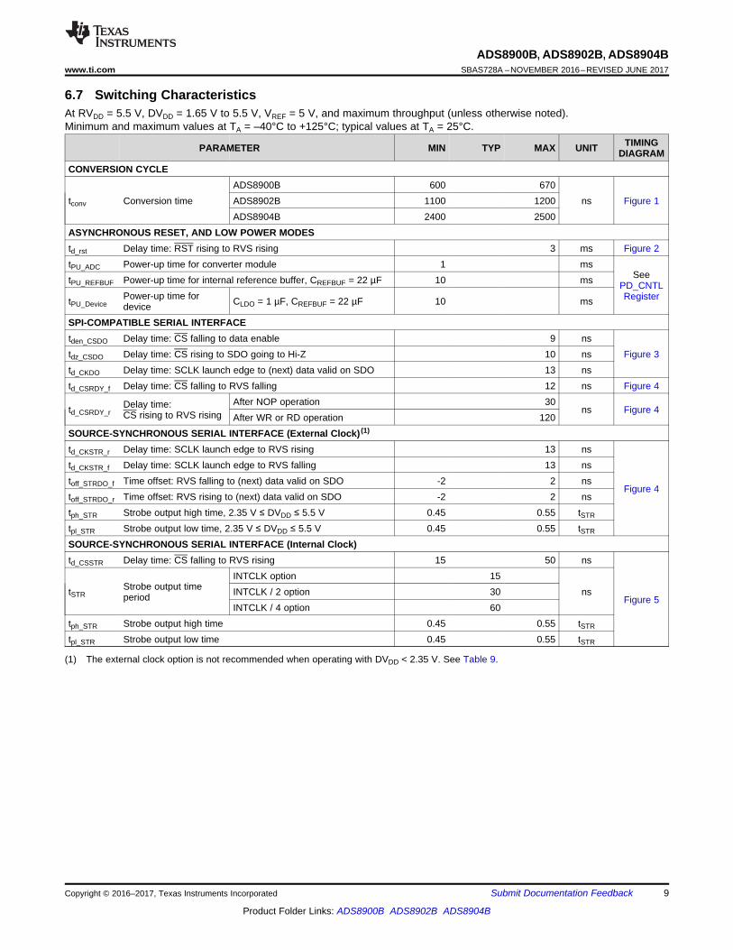
(1) The external clock option is not recommended when operating with DVDD < 2.35 V. See Table 9.
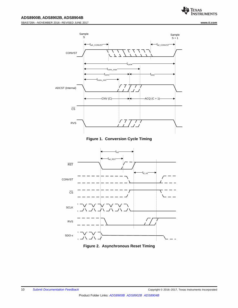
6.6 Timing RequirementsMIN TYP MAX UNIT TIMING
DIAGRAMCONVERSION CYCLE
fcycle Sampling frequencyADS8900B 1000
kHz
Figure 1
ADS8902B 500ADS8904B 250
tcycle ADC cycle-time periodADS8900B 1
µsADS8902B 2ADS8904B 4
twh_CONVST Pulse duration: CONVST high 30 nstwl_CONVST Pulse duration: CONVST low 30 nstacq Acquisition time 300 nstqt_acq Quiet acquisition time 30 ns Figure 46,
see DataTransferProtocols
td_cnvcap Quiet aperture time 20 ns
ASYNCHRONOUS RESET, AND LOW POWER MODEStwl_RST Pulse duration: RST low 100 ns Figure 2SPI-COMPATIBLE SERIAL INTERFACE
fCLK Serial clock frequency
2.35 V ≤ DVDD ≤ 5.5 V,TA = –40°C to +125°C,VIH > 0.7 DVDD, VIL < 0.3 DVDD
70
MHz Figure 3
1.65 V ≤ DVDD < 2.35 V,TA = –40°C to +125°C,VIH > 0.8 DVDD, VIL < 0.2 DVDD
20
1.65 V ≤ DVDD < 2.35 V,TA = 0°C to +60°C,VIH > 0.8 DVDD, VIL < 0.2 DVDD
57
1.65 V ≤ DVDD < 2.35 V,TA = –40°C to +125°C,VIH > 0.9 DVDD, VIL < 0.1 DVDD
68
tCLK Serial clock time period 1/fCLK ns Figure 3tph_CK SCLK high time 0.45 0.55 tCLK
Figure 3
tpl_CK SCLK low time 0.45 0.55 tCLK
tsu_CSCK Setup time: CS falling to the first SCLK capture edge 12 nstsu_CKDI Setup time: SDI data valid to the SCLK capture edge 1.5 nstht_CKDI Hold time: SCLK capture edge to (previous) data valid on SDI 1 nstht_CKCS Delay time: last SCLK falling to CS rising 7 nsSOURCE-SYNCHRONOUS SERIAL INTERFACE (External Clock) (1)
fCLK Serial clock frequency
SDR (DATA_RATE = 0b),2.35 V ≤ DVDD ≤ 5.5 V 70
MHzFigure 4,see DataTransferProtocols
DDR (DATA_RATE = 1b),2.35 V ≤ DVDD ≤ 5.5 V 35
tCLK Serial clock time period 1/fCLK ns
9
ADS8900B, ADS8902B, ADS8904Bwww.ti.com SBAS728A –NOVEMBER 2016–REVISED JUNE 2017
Product Folder Links: ADS8900B ADS8902B ADS8904B
Submit Documentation FeedbackCopyright © 2016–2017, Texas Instruments Incorporated
(1) The external clock option is not recommended when operating with DVDD < 2.35 V. See Table 9.
6.7 Switching CharacteristicsAt RVDD = 5.5 V, DVDD = 1.65 V to 5.5 V, VREF = 5 V, and maximum throughput (unless otherwise noted).Minimum and maximum values at TA = –40°C to +125°C; typical values at TA = 25°C.
PARAMETER MIN TYP MAX UNIT TIMINGDIAGRAM
CONVERSION CYCLE
tconv Conversion timeADS8900B 600 670
ns Figure 1ADS8902B 1100 1200ADS8904B 2400 2500
ASYNCHRONOUS RESET, AND LOW POWER MODEStd_rst Delay time: RST rising to RVS rising 3 ms Figure 2tPU_ADC Power-up time for converter module 1 ms
SeePD_CNTLRegister
tPU_REFBUF Power-up time for internal reference buffer, CREFBUF = 22 µF 10 ms
tPU_DevicePower-up time fordevice CLDO = 1 µF, CREFBUF = 22 µF 10 ms
SPI-COMPATIBLE SERIAL INTERFACEtden_CSDO Delay time: CS falling to data enable 9 ns
Figure 3tdz_CSDO Delay time: CS rising to SDO going to Hi-Z 10 nstd_CKDO Delay time: SCLK launch edge to (next) data valid on SDO 13 nstd_CSRDY_f Delay time: CS falling to RVS falling 12 ns Figure 4
td_CSRDY_rDelay time:CS rising to RVS rising
After NOP operation 30ns Figure 4
After WR or RD operation 120SOURCE-SYNCHRONOUS SERIAL INTERFACE (External Clock) (1)
td_CKSTR_r Delay time: SCLK launch edge to RVS rising 13 ns
Figure 4
td_CKSTR_f Delay time: SCLK launch edge to RVS falling 13 nstoff_STRDO_f Time offset: RVS falling to (next) data valid on SDO -2 2 nstoff_STRDO_r Time offset: RVS rising to (next) data valid on SDO -2 2 nstph_STR Strobe output high time, 2.35 V ≤ DVDD ≤ 5.5 V 0.45 0.55 tSTR
tpl_STR Strobe output low time, 2.35 V ≤ DVDD ≤ 5.5 V 0.45 0.55 tSTR
SOURCE-SYNCHRONOUS SERIAL INTERFACE (Internal Clock)td_CSSTR Delay time: CS falling to RVS rising 15 50 ns
Figure 5tSTR
Strobe output timeperiod
INTCLK option 15nsINTCLK / 2 option 30
INTCLK / 4 option 60tph_STR Strobe output high time 0.45 0.55 tSTR
tpl_STR Strobe output low time 0.45 0.55 tSTR
CONVST
RVS
twl_RST
SDO-x
RST
CS
trst
SCLK
td_rst
CONVST
ADCST (Internal)
tcycle
RVS
twh_CONVST twl_CONVST
tconv_min
tconv_max
CS
tconv tacq
Sample S
SampleS + 1
CNV (C) ACQ (C + 1)
10
ADS8900B, ADS8902B, ADS8904BSBAS728A –NOVEMBER 2016–REVISED JUNE 2017 www.ti.com
Product Folder Links: ADS8900B ADS8902B ADS8904B
Submit Documentation Feedback Copyright © 2016–2017, Texas Instruments Incorporated
Figure 1. Conversion Cycle Timing
Figure 2. Asynchronous Reset Timing

SCLK
SDO-x
CS
tsu_CSCK tht_CKCS
tden_CSDO tdz_CSDO
SCLK
RVS
SDO-x (DDR)
RVS
td_CSRDY_f td_CSRDY_r
tph_CK tpl_CK
tCLK
td_CKSTR_r
td_CKSTR_f
toff_STRDO_r
SDO-x (SDR)
toff_STRDO_r
toff_STRDO_f
SCLK(1)
SDO-x
tsu_CSCK tht_CKCS
tden_CSDO tdz_CSDO
SCLK(1)
SDI
SDO-x
tph_CK tpl_CK
tCLK
tsu_CKDI
tht_CKDI
td_CKDO
CS
11
ADS8900B, ADS8902B, ADS8904Bwww.ti.com SBAS728A –NOVEMBER 2016–REVISED JUNE 2017
Product Folder Links: ADS8900B ADS8902B ADS8904B
Submit Documentation FeedbackCopyright © 2016–2017, Texas Instruments Incorporated
(1) The SCLK polarity, launch edge, and capture edge depend on the SPI protocol selected.
Figure 3. SPI-Compatible Serial Interface Timing
Figure 4. Source-Synchronous Serial Interface Timing (External Clock)

SDO-x
tden_CSDO tdz_CSDO
RVS
SDO-x (DDR)
RVS
td_CSRDY_f td_CSRDY_r
tph_STR tpl_STR
tSTR
toff_STRDO_r
SDO-x (SDR)
toff_STRDO_r
toff_STRDO_f
td_CSSTR
CS
12
ADS8900B, ADS8902B, ADS8904BSBAS728A –NOVEMBER 2016–REVISED JUNE 2017 www.ti.com
Product Folder Links: ADS8900B ADS8902B ADS8904B
Submit Documentation Feedback Copyright © 2016–2017, Texas Instruments Incorporated
Figure 5. Source-Synchronous Serial Interface Timing (Internal Clock)

Free-Air Temperature (qC)
Diff
eren
tial N
onlin
earit
y (L
SB
)
-40 -7 26 59 92 125-1
-0.5
0
0.5
1
D003
MaximumMinimum
Free-Air Temperature (qC)
Inte
gral
Non
linea
rity
(LS
B)
-40 -7 26 59 92 125-4
-2
0
2
4
D004
MaximumMinimum
Fre
quen
cy
0
500
1000
1500
2000
2500
3000
3500
-0.5 -0.4 -0.3 -0.2 -0.1 0 0.1 0.2 0.3 0.4 0.5
D007
Fre
quen
cy
0
500
1000
1500
2000
2500
3000
-2 -1.5 -1 -0.5 0 0.5 1 1.5 2
D008
ADC Output Code
Diff
eren
tial N
onlin
earit
y (L
SB
)
-524288 524287-1
-0.5
0
0.5
1
D001ADC Output Code
Inte
gral
Non
linea
rity
(LS
B)
-524288 524287-2
-1
0
1
2
D002
13
ADS8900B, ADS8902B, ADS8904Bwww.ti.com SBAS728A –NOVEMBER 2016–REVISED JUNE 2017
Product Folder Links: ADS8900B ADS8902B ADS8904B
Submit Documentation FeedbackCopyright © 2016–2017, Texas Instruments Incorporated
6.8 Typical Characteristicsat TA = 25°C, RVDD = 5.5 V, DVDD = 3 V, VREF = 5 V, and maximum-rated throughput (unless otherwise noted)
Typical DNL = ±0.2 ppm
Figure 6. Typical DNL
Typical INL = ±0.75 ppm
Figure 7. Typical INL
3250 devices
Figure 8. Typical DNL Distribution (LSB)
3250 devices
Figure 9. Typical INL Distribution (LSB)
Figure 10. DNL vs Temperature Figure 11. INL vs Temperature

Free-Air Temperature (qC)
Offs
et (
LSB
)
-40 -7 26 59 92 125-10
-8
-6
-4
-2
0
2
4
6
8
10
D020Reference Voltage (V)
Offs
et (
mV
)
2.5 3 3.5 4 4.5 5-5
-3
-1
1
3
5
D021
Fre
quen
cy
0
200
400
600
800
1000
1200
1400
-10 -8 -6 -4 -2 0 2 4 6 8 10
D019
Fre
quen
cy
0
200
400
600
800
1000
1200
-0.0
1
-0.0
08
-0.0
06
-0.0
04
-0.0
02 00.
002
0.00
40.
006
0.00
80.
01
D022
Reference Voltage (V)
Diff
eren
tial N
onlin
earit
y (L
SB
)
2.5 3 3.5 4 4.5 5-1
-0.5
0
0.5
1
D005
MaximumMinimum
Reference Voltage (V)
Inte
gral
Non
linea
rity
(LS
B)
2.5 3 3.5 4 4.5 5-3
-2
-1
0
1
2
3
D006
MaximumMinimum
14
ADS8900B, ADS8902B, ADS8904BSBAS728A –NOVEMBER 2016–REVISED JUNE 2017 www.ti.com
Product Folder Links: ADS8900B ADS8902B ADS8904B
Submit Documentation Feedback Copyright © 2016–2017, Texas Instruments Incorporated
Typical Characteristics (continued)at TA = 25°C, RVDD = 5.5 V, DVDD = 3 V, VREF = 5 V, and maximum-rated throughput (unless otherwise noted)
Figure 12. DNL vs Reference Voltage Figure 13. INL vs Reference Voltage
3250 devices
Figure 14. Typical Offset Distribution (LSB)
3250 devices
Figure 15. Typical Gain Error Distribution (%FS)
REF_SEL[2:0] = 000b
Figure 16. Offset vs Temperature
With appropriate REF_SEL[2:0], see OFST_CAL
Figure 17. Offset vs Reference Voltage

fIN, Input Frequency (kHz)
Pow
er (
dB)
0 50 100 150 200 250-200
-150
-100
-50
0
D029 fIN, Input Frequency (kHz)
Pow
er (
dB)
0 25 50 75 100 125-200
-150
-100
-50
0
D030
Fre
quen
cy
0
200
400
600
800
5242
79
5242
81
5242
83
5242
85
5242
87
5242
89
5242
91
5242
93
5242
95
5242
97
D009 fIN, Input Frequency (kHz)
Pow
er (
dB)
0 100 200 300 400 500-200
-150
-100
-50
0
D011
Free-Air Temperature (qC)
Gai
n E
rror
(%
FS
)
-40 -7 26 59 92 125-0.02
-0.012
-0.004
0.004
0.012
0.02
D023
Gain (%FS) ADC onlyGain (%FS) ADC + REFBUF
Reference Voltage (V)
Gai
n E
rror
(%
FS
)
2.5 3 3.5 4 4.5 5-0.1
-0.05
0
0.05
0.1
D024
Gain (%FS) ADC onlyGain (%FS) ADC + REFBUF
15
ADS8900B, ADS8902B, ADS8904Bwww.ti.com SBAS728A –NOVEMBER 2016–REVISED JUNE 2017
Product Folder Links: ADS8900B ADS8902B ADS8904B
Submit Documentation FeedbackCopyright © 2016–2017, Texas Instruments Incorporated
Typical Characteristics (continued)at TA = 25°C, RVDD = 5.5 V, DVDD = 3 V, VREF = 5 V, and maximum-rated throughput (unless otherwise noted)
EN_MARG = 0b
Figure 18. Gain Error vs Temperature
EN_MARG = 0b
Figure 19. Gain Error vs Reference Voltage
Standard Deviation = 2 ppm
Figure 20. DC Input Histogram
fIN = 2 kHz SNR = 104.5 dB THD = –125 dB
Figure 21. Typical FFT - ADS8900B
fIN = 2 kHz SNR = 104.5 dB THD = –125 dB
Figure 22. Typical FFT - ADS8902B
fIN = 2 kHz SNR = 104.5 dB THD = –125 dB
Figure 23. Typical FFT - ADS8904B
fIN, Input Frequency (kHz)
SN
R, S
INA
D (
dBF
S)
EN
OB
(B
its)
0 100 200 300 400 50085 13
90 14
95 15
100 16
105 17
D017
SNRSINADENOB
fIN, Input Frequency (kHz)
TH
D (
dBF
S)
SF
DR
(dB
FS
)
0 100 200 300 400 500-130 90
-125 95
-120 100
-115 105
-110 110
-105 115
-100 120
-95 125
-90 130
D018
THDSFDR
Reference Voltage (V)
SN
R, S
INA
D (
dBF
S)
EN
OB
(B
its)
2.5 3 3.5 4 4.5 592 15.5
96 16
100 16.5
104 17
108 17.5
D015
SNRSINADENOB
Reference Voltage (V)
TH
D (
dBF
S)
SF
DR
(dB
FS
)
2.5 3 3.5 4 4.5 5-132 116
-128 120
-124 124
-120 128
-116 132
D016
THDSFDR
Free-Air Temperature (qC)
SN
R, S
INA
D (
dBF
S)
EN
OB
(Bits)
-40 -7 26 59 92 125102 16
103 16.5
104 17
105 17.5
106 18
D013
SNRSINADENOB
Free-Air Temperature (qC)
TH
D (
dBF
S)
SF
DR
(dB
FS
)
-40 -7 26 59 92 125-132 116
-128 120
-124 124
-120 128
-116 132
D014
THDSFDR
16
ADS8900B, ADS8902B, ADS8904BSBAS728A –NOVEMBER 2016–REVISED JUNE 2017 www.ti.com
Product Folder Links: ADS8900B ADS8902B ADS8904B
Submit Documentation Feedback Copyright © 2016–2017, Texas Instruments Incorporated
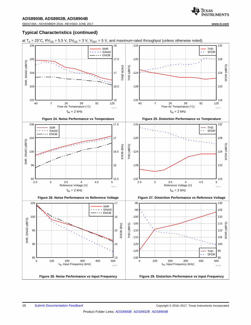
Typical Characteristics (continued)at TA = 25°C, RVDD = 5.5 V, DVDD = 3 V, VREF = 5 V, and maximum-rated throughput (unless otherwise noted)
fIN = 2 kHz
Figure 24. Noise Performance vs Temperature
fIN = 2 kHz
Figure 25. Distortion Performance vs Temperature
fIN = 2 kHz
Figure 26. Noise Performance vs Reference Voltage
fIN = 2 kHz
Figure 27. Distortion Performance vs Reference Voltage
Figure 28. Noise Performance vs Input Frequency Figure 29. Distortion Performance vs Input Frequency

RVDD (V)
I RV
DD
(m
A)
3 3.5 4 4.5 5 5.51
1.5
2
2.5
3
3.5
4
4.5
5
5.5
D026
ADS8900BADS8902BADS8904B
Free-Air Temperature (qC)
I RV
DD
(m
A)
-40 -7 26 59 92 1250
1
2
3
4
5
D028
ADS8900BADS8902BADS8904B
17
ADS8900B, ADS8902B, ADS8904Bwww.ti.com SBAS728A –NOVEMBER 2016–REVISED JUNE 2017
Product Folder Links: ADS8900B ADS8902B ADS8904B
Submit Documentation FeedbackCopyright © 2016–2017, Texas Instruments Incorporated
Typical Characteristics (continued)at TA = 25°C, RVDD = 5.5 V, DVDD = 3 V, VREF = 5 V, and maximum-rated throughput (unless otherwise noted)
Figure 30. Analog Supply Current vs Supply Voltage
RVDD = 5 V
Figure 31. Analog Supply Current vs Temperature
SAR ADC
LDO
BUF
GND
RVDD
DECAP
REFIN
REFBUFOUT
REFM
AINP
AINM
DVDD
multiSPITM
Digital Interface
ToDigitalHost
18
ADS8900B, ADS8902B, ADS8904BSBAS728A –NOVEMBER 2016–REVISED JUNE 2017 www.ti.com
Product Folder Links: ADS8900B ADS8902B ADS8904B
Submit Documentation Feedback Copyright © 2016–2017, Texas Instruments Incorporated
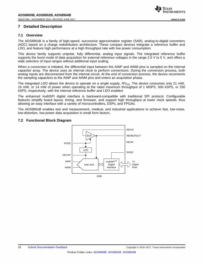
7 Detailed Description
7.1 OverviewThe ADS890xB is a family of high-speed, successive approximation register (SAR), analog-to-digital converters(ADC) based on a charge redistribution architecture. These compact devices integrate a reference buffer andLDO, and feature high performance at a high throughput rate with low power consumption.
This device family supports unipolar, fully differential, analog input signals. The integrated reference buffersupports the burst mode of data acquisition for external reference voltages in the range 2.5 V to 5 V, and offers awide selection of input ranges without additional input scaling.
When a conversion is initiated, the differential input between the AINP and AINM pins is sampled on the internalcapacitor array. The device uses an internal clock to perform conversions. During the conversion process, bothanalog inputs are disconnected from the internal circuit. At the end of conversion process, the device reconnectsthe sampling capacitors to the AINP and AINM pins and enters an acquisition phase.
The integrated LDO allows the device to operate on a single supply, RVDD. The device consumes only 21 mW,16 mW, or 14 mW of power when operating at the rated maximum throughput of 1 MSPS, 500 kSPS, or 250kSPS, respectively, with the internal reference buffer and LDO enabled.
The enhanced multiSPI digital interface is backward-compatible with traditional SPI protocol. Configurablefeatures simplify board layout, timing, and firmware, and support high throughput at lower clock speeds, thusallowing an easy interface with a variety of microcontrollers, DSPs, and FPGAs.
The ADS890xB enables test and measurement, medical, and industrial applications to achieve fast, low-noise,low-distortion, low-power data acquisition in small form factors.
7.2 Functional Block Diagram

LDO
GND
RVDD DECAP
CLDODECAP
1 �F
19
ADS8900B, ADS8902B, ADS8904Bwww.ti.com SBAS728A –NOVEMBER 2016–REVISED JUNE 2017
Product Folder Links: ADS8900B ADS8902B ADS8904B
Submit Documentation FeedbackCopyright © 2016–2017, Texas Instruments Incorporated
7.3 Feature DescriptionFrom a functional perspective, the device comprises four modules: the low-dropout regulator (LDO), thereference buffer (BUF), the converter (SAR ADC), and the interface (multiSPI digital interface), as shown in theFunctional Block Diagram section.
The LDO module is powered by the RVDD supply, and generates the bias voltage for internal circuit blocks of thedevice. The reference buffer module buffers the external reference voltage source from the dynamic, capacitiveswitching load present on the reference pins during the conversion process. The converter module samples andconverts the analog input into an equivalent digital output code. The interface module facilitates communicationand data transfer between the device and the host controller.
7.3.1 LDO ModuleTo enable single-supply operation, the device features an internal low-dropout regulator (LDO). The LDO ispowered by the RVDD supply, and the output is available on the two DECAP pins. This LDO output powers thecritical analog blocks within the device, and must not be used for any other external purposes.
Short the two DECAP pins together, and decouple with the GND pin by placing a 1-μF, X7R-grade, ceramiccapacitor with a 10-V rating, as shown in Figure 32. There is no upper limit on the value of the decouplingcapacitor; however, a larger decoupling capacitor results in a longer power-up time for the device. See theLayout section for layout recommendations.
Figure 32. Internal LDO Connections
7.3.2 Reference Buffer ModuleOn the CONVST rising edge, the device moves from ACQ state to CONV state, and the internal capacitors areswitched to the REFBUFOUT pins as per the successive approximation algorithm. Most of the switching chargerequired during the conversion process is provided by external decoupling capacitor CREFBUF. If the charge lostfrom the CREFBUF is not replenished before the next CONVST rising edge, the voltage on REFBUFOUT pins isless than VREFBUFOUT. The subsequent conversion occurs with this different reference voltage, and causes aproportional error in the output code. The internal reference buffer of the device maintains the voltage onREFBUFOUT pins within 0.5-LSB of VREFBUFOUT. All the performance characteristics of the device are specifiedwith the internal reference buffer and specified values of CREFBUF and RESR.
In burst-mode of operation, the device stays in ACQ state for a long duration of time and then performs a burst ofconversions. During the acquisition state (ACQ), the sampling capacitor (CS) is connected to the differential inputpins and no charge is drawn from the REFBUFOUT pins. However, during the very first conversion cycle, thereis a step change in the current drawn from the REFBUFOUT pins. This sudden change in load triggers atransient settling response in the reference buffer. For a fixed input voltage, any transient settling error at the endof the conversion cycle results in a change in output codes over the subsequent conversions, as shown inFigure 33. The internal reference buffer of the ADS89xxB, when used with the recommended values of CREFBUFand RESR, keeps the transient settling error at the end of each conversion cycle within 0.5-LSB. Therefore, thedevice supports burst-mode of operation with every conversion result being as per the datasheet specifications.

REFIN
REFMGND
RVDD
+
±
REFM
REFBUFOUT
REFBUFOUT
Margin
BUF
ADS89xxB
-15
-10
-5
0
5
10
0 100 200 300 400 500 600 700 800 900 1000
Dev
iatio
n F
rom
Fin
al V
alue
(LS
B)
Time (µs)
With External Series Reference Directly Driving SAR ADC
With External Reference Buffer Driving SAR ADC
With ADS890xB Internal Reference Buffer
20
ADS8900B, ADS8902B, ADS8904BSBAS728A –NOVEMBER 2016–REVISED JUNE 2017 www.ti.com
Product Folder Links: ADS8900B ADS8902B ADS8904B
Submit Documentation Feedback Copyright © 2016–2017, Texas Instruments Incorporated
Feature Description (continued)
Figure 33. ADC Output Codes in Burst-Mode Operation With Various ADC Reference Buffers
Figure 34 shows the block diagram of the internal reference buffer.
Figure 34. Internal Reference Buffer Block Diagram
The input range for the device is set by the external voltage applied at the REFIN pin (VREF). The REFIN pin haselectrostatic discharge (ESD) protection diodes to the RVDD and GND pins. For minimum input offset error (seeE(IO) specified in the Electrical Characteristics), set the REF_SEL[2:0] bits to the value closest to VREF (see theOFST_CAL register).
The internal reference buffer has a typical gain of 1 V/V with minimal offset error (see V(RO) specified in theElectrical Characteristics), and the output of the buffer is available between the REFBUFOUT pins and the REFMpins. Set the REF_OFST[4:0] bits to add or subtract an intentional offset voltage (see the REF_MRG register).
Figure 35 shows the external connections required for the internal reference buffer.
Converter Module
AINP
AINM
GND
REFP
AGND
Sample-and-Hold
Circuit
AVDD
ADC
OSC
Interface Module
DVDD
RST
CONVST
CS
SCLK
SDI
SDO-0
SDO-1
SDO-2
SDO-3
RVS
DGND
Conversion Result
ADCST
CONVST
RST
REFM
REFIN
REFMGND
RVDD
+
-
REFM
REFBUFOUT
REFBUFOUT
Margin
BUF
CREFBUF
RESR
VREFIREF
+VA
External Reference
Source
ADS89xxB
RREF_FLT
CREF_FLT
21
ADS8900B, ADS8902B, ADS8904Bwww.ti.com SBAS728A –NOVEMBER 2016–REVISED JUNE 2017
Product Folder Links: ADS8900B ADS8902B ADS8904B
Submit Documentation FeedbackCopyright © 2016–2017, Texas Instruments Incorporated
Feature Description (continued)
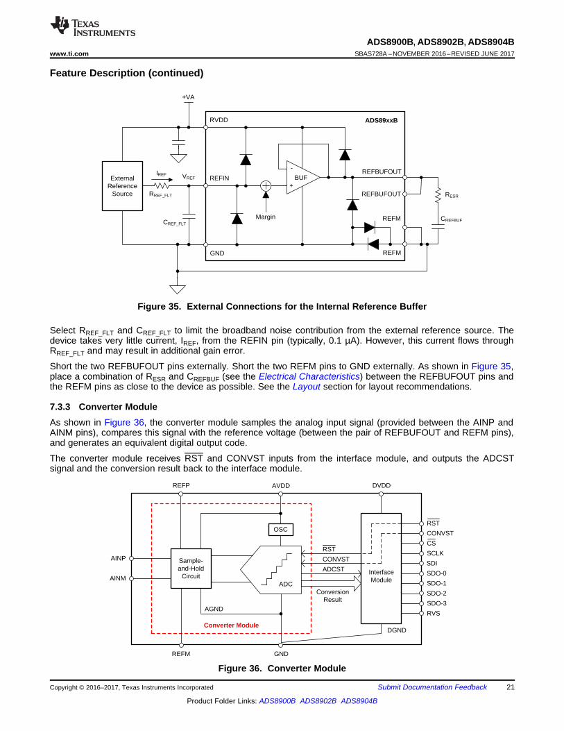
Figure 35. External Connections for the Internal Reference Buffer
Select RREF_FLT and CREF_FLT to limit the broadband noise contribution from the external reference source. Thedevice takes very little current, IREF, from the REFIN pin (typically, 0.1 µA). However, this current flows throughRREF_FLT and may result in additional gain error.
Short the two REFBUFOUT pins externally. Short the two REFM pins to GND externally. As shown in Figure 35,place a combination of RESR and CREFBUF (see the Electrical Characteristics) between the REFBUFOUT pins andthe REFM pins as close to the device as possible. See the Layout section for layout recommendations.
7.3.3 Converter ModuleAs shown in Figure 36, the converter module samples the analog input signal (provided between the AINP andAINM pins), compares this signal with the reference voltage (between the pair of REFBUFOUT and REFM pins),and generates an equivalent digital output code.
The converter module receives RST and CONVST inputs from the interface module, and outputs the ADCSTsignal and the conversion result back to the interface module.
Figure 36. Converter Module

.REFCM
VV 0 1 V
2§ ·
r¨ ¸© ¹
REFFSR V r
AINP
AINM
CS1
REFBUFOUT
Device in Hold Mode
CS2
RS1
4 pF
4 pF
SW1
RS2 SW2
GNDGND
22
ADS8900B, ADS8902B, ADS8904BSBAS728A –NOVEMBER 2016–REVISED JUNE 2017 www.ti.com
Product Folder Links: ADS8900B ADS8902B ADS8904B
Submit Documentation Feedback Copyright © 2016–2017, Texas Instruments Incorporated
Feature Description (continued)7.3.3.1 Sample-and-Hold CircuitThese devices support unipolar, fully differential, analog input signals. Figure 37 shows a small-signal equivalentcircuit of the sample-and-hold circuit. Each sampling switch is represented by a resistance (RS1 and RS2, typically50 Ω) in series with an ideal switch (SW1 and SW2). The sampling capacitors, CS1 and CS2, are typically 60 pF.
Figure 37. Input Sampling Stage Equivalent Circuit
During the acquisition process (ACQ state), both positive and negative inputs are individually sampled on CS1and CS2, respectively. During the conversion process (CNV state), the device converts for the voltage differencebetween the two sampled values: VAINP – VAINM.
Each analog input pin has electrostatic discharge (ESD) protection diodes to REFBUFOUT and GND. Keep theanalog inputs within the specified range to avoid turning the diodes on.
Equation 1 and Equation 2 show the full-scale input range (FSR) and common-mode voltage (VCM), respectively,supported at the analog inputs for any external reference voltage provided on the REFIN pin (VREF).
(1)
(2)

80001
7FFFF
00000
VREF ± 1 LSB0±VREF + 1 LSB
Differential Analog Input(AINP � AINM)
±1 LSB
FFFFF
AD
C C
ode
(Hex
)
VIN80000
REF20 20
VFSR1 LSB 2
2 2 u
23
ADS8900B, ADS8902B, ADS8904Bwww.ti.com SBAS728A –NOVEMBER 2016–REVISED JUNE 2017
Product Folder Links: ADS8900B ADS8902B ADS8904B
Submit Documentation FeedbackCopyright © 2016–2017, Texas Instruments Incorporated
Feature Description (continued)7.3.3.2 Internal OscillatorThe device family features an internal oscillator (OSC) that provides the conversion clock; see Figure 36. Theconversion duration is bound by the minimum and maximum value of tconv, as specified in the SwitchingCharacteristics table.
The interface module uses this internal clock (OSC), an external clock (provided by the host controller on theSCLK pin), or a combination of both the internal and external clocks, to execute the data transfer operationsbetween the device and host controller; see the Interface Module section for more details.
7.3.3.3 ADC Transfer FunctionThe device family supports unipolar, fully differential analog inputs. The device output is in two's complimentformat. Figure 38 and Table 1 show the ideal transfer characteristics for the device.
The least significant bit (LSB) for the ADC is given by Equation 3:
(3)
Figure 38. Differential Transfer Characteristics
Table 1. Transfer CharacteristicsDIFFERENTIAL ANALOG INPUT VOLTAGE
(AINP – AINM)OUTPUT CODE
(HEX)< –VREF 80000
–VREF + 1 LSB 80001–1 LSB FFFFF
0 000001 LSB 00001
> VREF – 1 LSB 7FFFF

Interface Module
Configuration Registers
Command ProcessorSCLK
Counter
Pro
toco
l
Converter Module
Output Data Register (ODR)
Input Data Register (IDR)
22 Bits
22 Bits
Shift Registers
D21 D20 D1 D0
B21 B20 B1 B0
RST
CONVST
CS
SCLK
SDI
SDO-0
SDO-1
SDO-2
SDO-3
RVS
24
ADS8900B, ADS8902B, ADS8904BSBAS728A –NOVEMBER 2016–REVISED JUNE 2017 www.ti.com
Product Folder Links: ADS8900B ADS8902B ADS8904B
Submit Documentation Feedback Copyright © 2016–2017, Texas Instruments Incorporated
7.3.4 Interface ModuleThe interface module facilitates the communication and data transfer between the device and the host controller.As shown in Figure 39, the module consists of shift registers (both input and output), configuration registers, anda protocol unit.
Figure 39. Interface Module
The Pin Configuration and Functions section provides descriptions of the interface pins. The Data TransferFrame section details the functions of shift registers, the SCLK counter, and the command processor. The DataTransfer Protocols section details supported protocols. The Register Maps section explains the configurationregisters and bit settings.

CONVST
RVS
twl_RST
SDO-x
RST
CS
trst
SCLK
td_rst
ACQ
CNV RST
Power Up
CONVST Rising Edge
End of Conversion
RST Falling Edge
RST Rising Edge
RST Falling Edge
25
ADS8900B, ADS8902B, ADS8904Bwww.ti.com SBAS728A –NOVEMBER 2016–REVISED JUNE 2017
Product Folder Links: ADS8900B ADS8902B ADS8904B
Submit Documentation FeedbackCopyright © 2016–2017, Texas Instruments Incorporated
7.4 Device Functional ModesAs shown in Figure 40, this device family supports three functional states: RST, ACQ, and CNV. The devicestate is determined by the status of the CONVST and RST control signals provided by the host controller.
Figure 40. Device Functional States
7.4.1 RST StateThe RST pin is an asynchronous digital input for the device. To enter RST state, the host controller pulls the RSTpin low and keeps it low for the twl_RST duration (as specified in the Timing Requirements table).
In RST state, all configuration registers (see the Register Maps section) are reset to their default values, the RVSpin remains low, and the SDO-x pins are Hi-Z.
To exit RST state, the host controller pulls the RST pin high, with CONVST and SCLK held low and CS heldhigh, as shown in Figure 41. After a delay of td_rst, the device enters ACQ state and the RVS pin goes high.
Figure 41. Asynchronous Reset
To operate the device in either ACQ or CNV state, RST must be held high. With RST held high, transitions onthe CONVST pin determine the functional state of the device.
cycle-min conv acq-mint t t �
CONVST
ADCST (Internal)
tcycle
RVS
twh_CONVST twl_CONVST
tconv_min
tconv_max
CS
tconv tacq
Sample S
SampleS + 1
CNV (C) ACQ (C + 1)
26
ADS8900B, ADS8902B, ADS8904BSBAS728A –NOVEMBER 2016–REVISED JUNE 2017 www.ti.com
Product Folder Links: ADS8900B ADS8902B ADS8904B
Submit Documentation Feedback Copyright © 2016–2017, Texas Instruments Incorporated
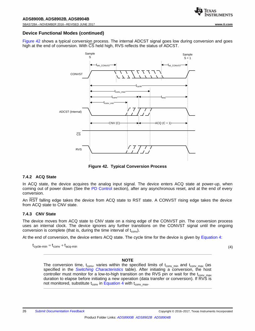
Device Functional Modes (continued)Figure 42 shows a typical conversion process. The internal ADCST signal goes low during conversion and goeshigh at the end of conversion. With CS held high, RVS reflects the status of ADCST.
Figure 42. Typical Conversion Process
7.4.2 ACQ StateIn ACQ state, the device acquires the analog input signal. The device enters ACQ state at power-up, whencoming out of power down (See the PD Control section), after any asynchronous reset, and at the end of everyconversion.
An RST falling edge takes the device from ACQ state to RST state. A CONVST rising edge takes the devicefrom ACQ state to CNV state.
7.4.3 CNV StateThe device moves from ACQ state to CNV state on a rising edge of the CONVST pin. The conversion processuses an internal clock. The device ignores any further transitions on the CONVST signal until the ongoingconversion is complete (that is, during the time interval of tconv).
At the end of conversion, the device enters ACQ state. The cycle time for the device is given by Equation 4:
(4)
NOTEThe conversion time, tconv, varies within the specified limits of tconv_min and tconv_max (asspecified in the Switching Characteristics table). After initiating a conversion, the hostcontroller must monitor for a low-to-high transition on the RVS pin or wait for the tconv_maxduration to elapse before initiating a new operation (data transfer or conversion). If RVS isnot monitored, substitute tconv in Equation 4 with tconv_max.
27
ADS8900B, ADS8902B, ADS8904Bwww.ti.com SBAS728A –NOVEMBER 2016–REVISED JUNE 2017
Product Folder Links: ADS8900B ADS8902B ADS8904B
Submit Documentation FeedbackCopyright © 2016–2017, Texas Instruments Incorporated
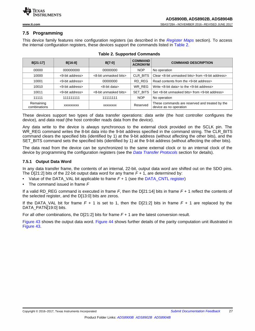
7.5 ProgrammingThis device family features nine configuration registers (as described in the Register Maps section). To accessthe internal configuration registers, these devices support the commands listed in Table 2.
Table 2. Supported Commands
B[21:17] B[16:8] B[7:0] COMMANDACRONYM COMMAND DESCRIPTION
00000 000000000 00000000 NOP No operation10000 <9-bit address> <8-bit unmasked bits> CLR_BITS Clear <8-bit unmasked bits> from <9-bit address>10001 <9-bit address> 00000000 RD_REG Read contents from the <9-bit address>10010 <9-bit address> <8-bit data> WR_REG Write <8-bit data> to the <9-bit address>10011 <9-bit address> <8-bit unmasked bits> SET_BITS Set <8-bit unmasked bits> from <9-bit address>11111 111111111 11111111 NOP No operation
Remainingcombinations xxxxxxxxx xxxxxxxx Reserved These commands are reserved and treated by the
device as no operation
These devices support two types of data transfer operations: data write (the host controller configures thedevice), and data read (the host controller reads data from the device).
Any data write to the device is always synchronous to the external clock provided on the SCLK pin. TheWR_REG command writes the 8-bit data into the 9-bit address specified in the command string. The CLR_BITScommand clears the specified bits (identified by 1) at the 9-bit address (without affecting the other bits), and theSET_BITS command sets the specified bits (identified by 1) at the 9-bit address (without affecting the other bits).
The data read from the device can be synchronized to the same external clock or to an internal clock of thedevice by programming the configuration registers (see the Data Transfer Protocols section for details).
7.5.1 Output Data WordIn any data transfer frame, the contents of an internal, 22-bit, output data word are shifted out on the SDO pins.The D[21:2] bits of the 22-bit output data word for any frame F + 1, are determined by:• Value of the DATA_VAL bit applicable to frame F + 1 (see the DATA_CNTL register)• The command issued in frame F
If a valid RD_REG command is executed in frame F, then the D[21:14] bits in frame F + 1 reflect the contents ofthe selected register, and the D[13:0] bits are zeros.
If the DATA_VAL bit for frame F + 1 is set to 1, then the D[21:2] bits in frame F + 1 are replaced by theDATA_PATN[19:0] bits.
For all other combinations, the D[21:2] bits for frame F + 1 are the latest conversion result.
Figure 43 shows the output data word. Figure 44 shows further details of the parity computation unit illustrated inFigure 43.

D21
D20
D3
D2
D0
D1Parity Computation Unit
Output Data Word D[21:0]
D[21:2]
0
1
20-bit Conversion Result
20-bit DATA_PATN[19:0]
Register Data<8-bit REGDATA>_<12-bit 0's>
A valid RG_READ command is received in the previous frame?
DATA_VAL
No
Yes
28
ADS8900B, ADS8902B, ADS8904BSBAS728A –NOVEMBER 2016–REVISED JUNE 2017 www.ti.com
Product Folder Links: ADS8900B ADS8902B ADS8904B
Submit Documentation Feedback Copyright © 2016–2017, Texas Instruments Incorporated
Figure 43. Output Data Word (D[21:0])
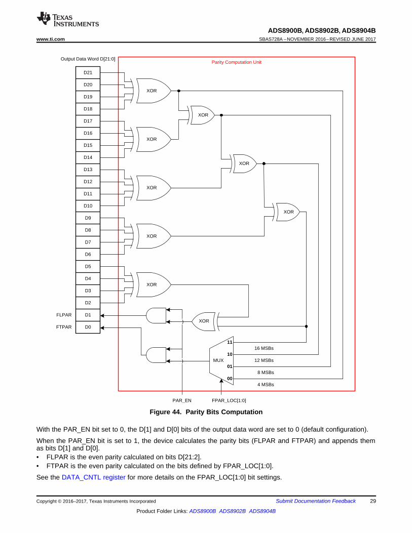
Parity Computation Unit
D21
D20
D19
D18
D17
D16
D15
D14
D13
D12
D11
D10
D9
D8
D7
D6
D5
D4
D3
D2
FLPAR
FTPAR
4 MSBs
8 MSBs
12 MSBs
16 MSBs
00
01
10
11
MUX
FPAR_LOC[1:0]
XOR
XOR
XOR
XOR
Output Data Word D[21:0]
PAR_EN
)
XOR
XOR
XOR
)
D1
D0XOR
XOR
29
ADS8900B, ADS8902B, ADS8904Bwww.ti.com SBAS728A –NOVEMBER 2016–REVISED JUNE 2017
Product Folder Links: ADS8900B ADS8902B ADS8904B
Submit Documentation FeedbackCopyright © 2016–2017, Texas Instruments Incorporated
Figure 44. Parity Bits Computation
With the PAR_EN bit set to 0, the D[1] and D[0] bits of the output data word are set to 0 (default configuration).
When the PAR_EN bit is set to 1, the device calculates the parity bits (FLPAR and FTPAR) and appends themas bits D[1] and D[0].• FLPAR is the even parity calculated on bits D[21:2].• FTPAR is the even parity calculated on the bits defined by FPAR_LOC[1:0].
See the DATA_CNTL register for more details on the FPAR_LOC[1:0] bit settings.

CONVSTFrame F
RVS
CS
td_CSRDY_r
SCLK
SDI Valid Command
As per output protocol selection.
N SCLKs
SDO-xODR Data
Output Data Word
Output Data Register (ODR)
D0
D21 D0
D21
0
SCLK Counter
N
SCLK Counter
Input Data Register (IDR)
Command Processor
D0
B21 B0
D21
30
ADS8900B, ADS8902B, ADS8904BSBAS728A –NOVEMBER 2016–REVISED JUNE 2017 www.ti.com
Product Folder Links: ADS8900B ADS8902B ADS8904B
Submit Documentation Feedback Copyright © 2016–2017, Texas Instruments Incorporated
7.5.2 Data Transfer FrameA data transfer frame between the device and the host controller is bounded between a CS falling edge and thesubsequent CS rising edge. The host controller can initiate a data transfer frame (as shown in Figure 45) at anytime irrespective of the status of the CONVST signal; however, the data read during such a data transfer frame isa function of relative timing between the CONVST and CS signals.
Figure 45. Data Transfer Frame
For this discussion, assume that the CONVST signal remains low.
A typical data transfer frame F follows this order:1. The host controller pulls CS low to initiate a data transfer frame. On the CS falling edge:
– RVS goes low, indicating the beginning of the data transfer frame.– The SCLK counter is reset to 0.– The device takes control of the data bus. As shown in Figure 45, the 22-bit contents of the output data
word (see Figure 43) are loaded in to the 22-bit output data register (ODR; see Figure 39).– The 22-bit input data register (IDR; see Figure 39) is reset to 000000h, corresponding to a NOP
command.
31
ADS8900B, ADS8902B, ADS8904Bwww.ti.com SBAS728A –NOVEMBER 2016–REVISED JUNE 2017
Product Folder Links: ADS8900B ADS8902B ADS8904B
Submit Documentation FeedbackCopyright © 2016–2017, Texas Instruments Incorporated
2. During the frame, the host controller provides clocks on the SCLK pin. Inside the device:– For each SCLK capture edge, the SCLK counter is incremented and the data bit received on the SDI pin
is shifted in to the IDR.– For each launch edge of the output clock (SCLK in this case), ODR data are shifted out on the selected
SDO-x pins.– The status of the RVS pin depends on the output protocol selection (see the Protocols for Reading From
the Device section).3. The host controller pulls CS high to end the data transfer frame. On the CS rising edge:
– The SDO-x pins go to Hi-Z.– RVS goes high (after a delay of td_CSRDY_r).– As illustrated in Figure 45, the 22-bit contents of the IDR are transferred to the command processor (see
Figure 39) for decoding and further action.
After pulling CS high, the host controller monitors for a low-to-high transition on the RVS pin, or waits for thetd_CSRDY_r time (see the Switching Characteristics table) to elapse before initiating a new operation (data transferor conversion). The delay, td_CSRDY_r, for any data transfer frame F varies based on the data transfer operationexecuted in frame F.
At the end of data transfer frame F:• If the SCLK counter is < 22, then the IDR captured less than 22 bits from the SDI. In this case, the device
treats frame F as a short command frame. At the end of a short command frame, the IDR is not updated andthe device treats the frame as a no operation (NOP) command.
• If the SCLK counter = 22, then the IDR captured exactly 22 bits from SDI. In this case, the device treats theframe F as a optimal command frame. At the end of an optimal command frame, the command processordecodes the 22-bit contents of the IDR as a valid command word.
• If the SCLK counter > 22, then the IDR captured more than 22 bits from the SDI; however, only the last 22bits are retained. In this case, the device treats frame F as a long command frame. At the end of a longcommand frame, the command processor treats the 22-bit contents of the IDR as a valid command word.There is no restriction on the maximum number of clocks that can be provided within any data transfer frameF. However, as explained above, make sure that the last 22 bits shifted into the device before the CS risingedge constitute the desired command.
In a short command frame, the write operation to the device is invalidated; however, the output data bitstransferred during the short command frame are still valid output data. Therefore, the host controller can usesuch shorter data transfer frames to read only the required number of MSB bits from the 22-bit output data word.As shown in Figure 43, an optimal read frame for the ADS890xB devices must read only the 20 MSB bits of theoutput data word. The length of an optimal read frame depends on the output protocol selection; see theProtocols for Reading From the Device section for more details.
NOTEThe previous example shows data-read and data-write operations synchronous to theexternal clock provided on the SCLK pin.
However, the device also supports data read operation synchronous to the internal clock;see the Protocols for Reading From the Device section for more details. In this case, whilethe ODR contents are shifted on the SDO (or SDOs) on the launch edge of the internalclock, the device continues to capture the SDI data into the IDR (and increment the SCLKcounter) on SCLK capture edges.
cycle d_cnvcapt t� cycle cycle qt_acqt t t� �
cycle qt_acqt t�convt
CONVST
ADCST(Internal)
tcycle
tconv tacq
ConversionC
ConversionC + 1
ConversionC + 2
tqt_acq
td_cnvcap
Zone 1 Zone 2
t = 0
SampleS
SampleS + 1
SampleS + 2
32
ADS8900B, ADS8902B, ADS8904BSBAS728A –NOVEMBER 2016–REVISED JUNE 2017 www.ti.com
Product Folder Links: ADS8900B ADS8902B ADS8904B
Submit Documentation Feedback Copyright © 2016–2017, Texas Instruments Incorporated
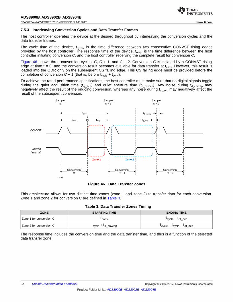
7.5.3 Interleaving Conversion Cycles and Data Transfer FramesThe host controller operates the device at the desired throughput by interleaving the conversion cycles and thedata transfer frames.
The cycle time of the device, tcycle, is the time difference between two consecutive CONVST rising edgesprovided by the host controller. The response time of the device, tresp, is the time difference between the hostcontroller initiating conversion C, and the host controller receiving the complete result for conversion C.
Figure 46 shows three conversion cycles: C, C + 1, and C + 2. Conversion C is initiated by a CONVST risingedge at time t = 0, and the conversion result becomes available for data transfer at tconv. However, this result isloaded into the ODR only on the subsequent CS falling edge. This CS falling edge must be provided before thecompletion of conversion C + 1 (that is, before tcycle + tconv).
To achieve the rated performance specifications, the host controller must make sure that no digital signals toggleduring the quiet acquisition time (tqt_acq) and quiet aperture time (td_cnvcap). Any noise during td_cnvcap maynegatively affect the result of the ongoing conversion, whereas any noise during tqt_acq may negatively affect theresult of the subsequent conversion.
Figure 46. Data Transfer Zones
This architecture allows for two distinct time zones (zone 1 and zone 2) to transfer data for each conversion.Zone 1 and zone 2 for conversion C are defined in Table 3.
Table 3. Data Transfer Zones TimingZONE STARTING TIME ENDING TIME
Zone 1 for conversion C
Zone 2 for conversion C
The response time includes the conversion time and the data transfer time, and thus is a function of the selecteddata transfer zone.

CONVST
ADCST(Internal)
tcycle
tconv tacq
ConversionC
ConversionC + 1
ConversionC + 2
tqt_acq
td_cnvcap
t = 0
SampleS
SampleS + 1
SampleS + 2
CS
FrameF
FrameF + 1
FrameF + 2
Zone 2C
Zone 2C + 1
Zone 2C + 2
SDOtresp-Z2
SCLK
tread-Z2
C ± 1 C C + 1
CONVST
ADCST(Internal)
tcycle
tconv tacq
ConversionC
ConversionC + 1
ConversionC + 2
tqt_acq
td_cnvcap
Zone 1C
t = 0
SampleS
SampleS + 1
SampleS + 2
CS
Zone 1C + 1
Zone 1C + 2
tread-Z1
FrameF
FrameF + 1
FrameF + 2
SDOtresp-Z1
C C + 1 C + 2
SCLK
33
ADS8900B, ADS8902B, ADS8904Bwww.ti.com SBAS728A –NOVEMBER 2016–REVISED JUNE 2017
Product Folder Links: ADS8900B ADS8902B ADS8904B
Submit Documentation FeedbackCopyright © 2016–2017, Texas Instruments Incorporated
Figure 47 and Figure 48 illustrate interleaving of three conversion cycles (C, C + 1, and C + 2) with three datatransfer frames (F, F + 1, and F + 2) in zone 1 and in zone 2, respectively.
Figure 47. Zone 1 Data Transfer
Figure 48. Zone 2 Data Transfer
resp-Z2-min cycle d_cnvcap read-Z2t t t t � �
tSCLKread_Z2
20f
t
read-Z2 cycle d_cnvcap qt_acqt t t td � �
resp-Z1-min conv read-Z1t t t �
tSCLKread-Z1
20f
t
read-Z1 cycle conv qt_acqt t t td � �
34
ADS8900B, ADS8902B, ADS8904BSBAS728A –NOVEMBER 2016–REVISED JUNE 2017 www.ti.com
Product Folder Links: ADS8900B ADS8902B ADS8904B
Submit Documentation Feedback Copyright © 2016–2017, Texas Instruments Incorporated
To achieve cycle time tcycle, the read time in zone 1 is given by Equation 5:
(5)
For an optimal data transfer frame, Equation 5 results in an SCLK frequency given by Equation 6:
(6)
Then, the zone 1 data transfer achieves a response time defined by Equation 7:
(7)
At lower SCLK speeds, tread-Z1 increases, resulting in slower response times and higher cycle times.
To achieve the same cycle time, tcycle, the read time in zone 2 is given by Equation 8:
(8)
For an optimal data transfer frame, Equation 8 results in an SCLK frequency given by Equation 9:
(9)
Then, the zone 2 data transfer achieves a response time defined by Equation 10:
(10)
Any increase in tread-Z2 increases response time and may increase cycle time.
For a given cycle time, the zone 1 data transfer clearly achieves faster response time, but also requires a higherSCLK speed (as evident from Equation 5, Equation 6, and Equation 7); whereas, the zone 2 data transfer clearlyrequires a lower SCLK speed but has a slower response time (as evident from Equation 8, Equation 9, andEquation 10).
NOTEA data transfer frame can begin in zone 1, and then extend into zone 2; however, the hostcontroller must make sure that no digital transitions occur during the tqt_acq and td_cnvcaptime intervals.
NOTEFor data transfer operations in zone 2 using the ADC-Clock-Master protocol(SDO_MODE[1:0] = 11b), the device supports only the external-clock-echo option(SSYNC_CLK_SEL[1:0] = 00b); see Table 9.
7.5.4 Data Transfer ProtocolsThis device family features a multiSPI digital interface that allows the host controller to operate at slower SCLKspeeds and still achieve the required throughput and response time. The multiSPI digital interface module offersthree options to reduce the SCLK speed required for data transfer:• Increase the width of the output data bus.• Enable double data rate (DDR) transfer.• Extended data transfer window, as shown in Figure 48.
These three options can be combined to achieve further reduction in SCLK speed.

_d_total_serial pcb_CK d_iso d_ckdo d_iso pcb_SDO su_h d delcapt t t t t t t t � � � � � �
SCLK
SDO-x
Device Host Controller
SCLK
SDI
tpcb_CK
tpcb_SDO
td_ISO
td_ISO
Digital Isolator (Optional)
tsu_htd_ckdo
td_delcap
clk-SPId_total-serial
1f
2 td
u
d_total_serial pcb_CK d_iso d_ckdo d_iso pcb_SDO su_ht t t t t t t � � � � �
SCLK
SDO-x
TI Device Host Controller
SCLK
SDI
tpcb_CK
tpcb_SDO
td_ISO
td_ISO
Digital Isolator (Optional)
tsu_htd_ckdo
Copyright © 2016, Texas Instruments Incorporated
35
ADS8900B, ADS8902B, ADS8904Bwww.ti.com SBAS728A –NOVEMBER 2016–REVISED JUNE 2017
Product Folder Links: ADS8900B ADS8902B ADS8904B
Submit Documentation FeedbackCopyright © 2016–2017, Texas Instruments Incorporated
There are various factors that limit the maximum SCLK frequency in a system.
Figure 49 shows the delays in the communication channel between the host controller and the device in a typicalserial communication.
Figure 49. Delays in Serial Communication
For example, if tpcb_CK and tpcb_SDO are the delays introduced by the printed circuit board (PCB) traces for theserial clock and SDO signals, td_CKDO is the clock-to-data delay of the device, td_ISO is the propagation delayintroduced by the digital isolator, and tsu_h is the setup time specification of the host controller, then the totaldelay in the path is given by Equation 11:
(11)
In a standard SPI protocol, the host controller and the device launch and capture data bits on alternate SCLKedges. Therefore, the td_total_serial delay must be kept to less than half of the SCLK duration. Equation 12 showsthe fastest clock allowed by the SPI protocol:
(12)
Larger values of the td_total_serial delay restricts the maximum SCLK speed for the SPI protocol, resulting in higherread and response times, and can possibly limit the throughput.
Figure 50 shows a delay (td_delcap) introduced in the capture path (inside the host controller).
Figure 50. Delayed Capture
The total delay in the path modifies to Equation 13:
(13)
This reduction in total delay allows the SPI protocol to operate at higher clock speeds.
d_total_srcsync pcb_RVS pcb_SDO su_ht t t t � �
SCLK
SDO-x
TI Device Host Controller
SCLK
SDI
tpcb_CK
tpcb_SDO
td_ISO
td_ISO
Digital Isolator (Optional)
RVStd_ISO
tpcb_RVS
td_ckdo
td_ckstr
tsu_htoff_strdo
Copyright © 2016, Texas Instruments Incorporated
clk-SPId_total-serial
1f
td
36
ADS8900B, ADS8902B, ADS8904BSBAS728A –NOVEMBER 2016–REVISED JUNE 2017 www.ti.com
Product Folder Links: ADS8900B ADS8902B ADS8904B
Submit Documentation Feedback Copyright © 2016–2017, Texas Instruments Incorporated
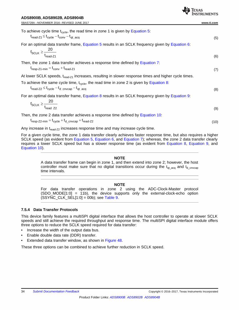
The multiSPI digital interface module offers two additional options to remove the restriction on the SCLK speed:• Early data launch (EDL) mode of operation
In EDL mode, the device launches the output data on SDO-x pin (or pins) half a clock earlier compared to thestandard SPI protocol. Therefore, Equation 12 modifies to Equation 14:
(14)The reduction in total delay allows the serial interface to operate at higher clock speeds.
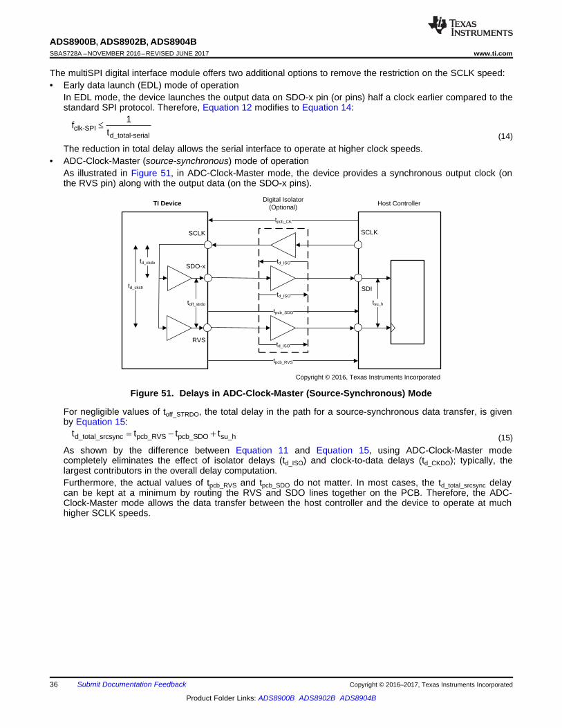
• ADC-Clock-Master (source-synchronous) mode of operationAs illustrated in Figure 51, in ADC-Clock-Master mode, the device provides a synchronous output clock (onthe RVS pin) along with the output data (on the SDO-x pins).
Figure 51. Delays in ADC-Clock-Master (Source-Synchronous) Mode
For negligible values of toff_STRDO, the total delay in the path for a source-synchronous data transfer, is givenby Equation 15:
(15)As shown by the difference between Equation 11 and Equation 15, using ADC-Clock-Master modecompletely eliminates the effect of isolator delays (td_ISO) and clock-to-data delays (td_CKDO); typically, thelargest contributors in the overall delay computation.Furthermore, the actual values of tpcb_RVS and tpcb_SDO do not matter. In most cases, the td_total_srcsync delaycan be kept at a minimum by routing the RVS and SDO lines together on the PCB. Therefore, the ADC-Clock-Master mode allows the data transfer between the host controller and the device to operate at muchhigher SCLK speeds.

SCLK
SDI
CS
B0B1B20 B19B21
RVS
SCLK
SDI
CS
RVS
B0B1B20 B2B21
SCLK
SDI
CS
B0B1B19B21
RVS
B20
SCLK
SDI
CS
B0B1B21 B20
RVS
37
ADS8900B, ADS8902B, ADS8904Bwww.ti.com SBAS728A –NOVEMBER 2016–REVISED JUNE 2017
Product Folder Links: ADS8900B ADS8902B ADS8904B
Submit Documentation FeedbackCopyright © 2016–2017, Texas Instruments Incorporated
7.5.4.1 Protocols for Configuring the DeviceAs shown in Table 4, the host controller can use any of the four legacy, SPI-compatible protocols (SPI-00-S, SPI-01-S, SPI-10-S, or SPI-11-S) to write data to the device.
Table 4. SPI Protocols for Configuring the Device
PROTOCOL SCLK POLARITY(At CS Falling Edge)
SCLK PHASE(Capture Edge) SDI_CNTL SDO_CNTL
NO. OF SCLK(Optimal Command
Frame)TIMING
DIAGRAM
SPI-00-S Low Rising 00h 00h 22 Figure 52SPI-01-S Low Falling 01h 00h 22 Figure 53SPI-10-S High Falling 02h 00h 22 Figure 54SPI-11-S High Rising 03h 00h 22 Figure 55
At power-up or after coming out of any asynchronous reset, the device supports the SPI-00-S protocol for data-read and data-write operations.
To select a different SPI-compatible protocol, program the SDI_MODE[1:0] bits in the SDI_CNTL register. Thisfirst write operation must adhere to the SPI-00-S protocol. Any subsequent data transfer frames must adhere tothe newly selected protocol.
Figure 52 to Figure 55 detail the four protocols using an optimal command frame; see the Timing Requirementsand Switching Characteristics tables for associated timing parameters.
NOTEAs explained in the Data Transfer Frame section, a valid write operation to the devicerequires a minimum of 22 SCLKs to be provided within a data transfer frame.
Any data write operation to the device must continue to follow the SPI-compatible protocolselected in the SDI_CNTL register, irrespective of the protocol selected for the data-readoperation.
Figure 52. SPI-00-S Protocol, Optimal CommandFrame
Figure 53. SPI-01-S Protocol, Optimal CommandFrame
Figure 54. SPI-10-S Protocol, Optimal CommandFrame
Figure 55. SPI-11-S Protocol, Optimal CommandFrame
SCLK
SDO-0 D21 D20 D1 D0
D21
D20
D20
D19
D1
D1 D0
D0
D21
0
CS
D2
D2
RVS
SCLK
D21
SDO-0 D21 D20 D1 D0
D20 D19 D0
D1 D0D21 D20 D19
CS
D1
RVS
SCLK
SDO-0 0 D21 D20 D1 D0
D21 D20
D21 D20
D19 D0
D1 D0
CS
RVS
SCLK
SDO-0 D21 D20 D1 D0
D21
D20
D20
D19
D19 D1
D1 D0
D0
D21CS
RVS
38
ADS8900B, ADS8902B, ADS8904BSBAS728A –NOVEMBER 2016–REVISED JUNE 2017 www.ti.com
Product Folder Links: ADS8900B ADS8902B ADS8904B
Submit Documentation Feedback Copyright © 2016–2017, Texas Instruments Incorporated
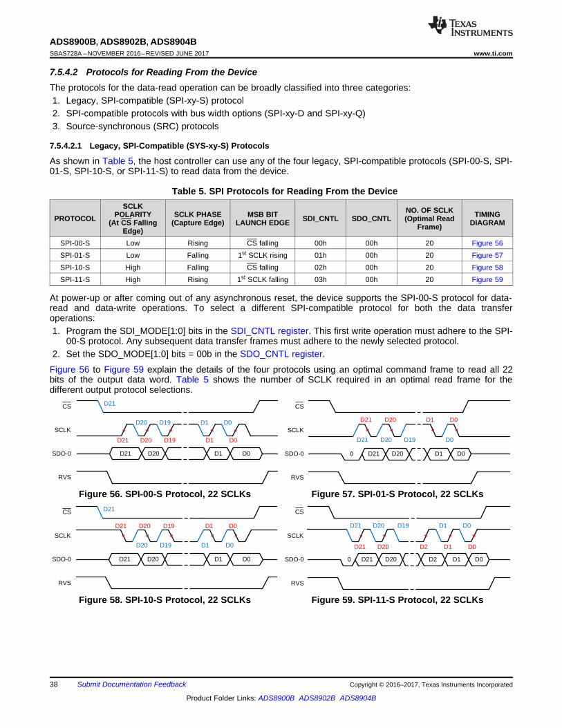
7.5.4.2 Protocols for Reading From the DeviceThe protocols for the data-read operation can be broadly classified into three categories:1. Legacy, SPI-compatible (SPI-xy-S) protocol2. SPI-compatible protocols with bus width options (SPI-xy-D and SPI-xy-Q)3. Source-synchronous (SRC) protocols
7.5.4.2.1 Legacy, SPI-Compatible (SYS-xy-S) Protocols
As shown in Table 5, the host controller can use any of the four legacy, SPI-compatible protocols (SPI-00-S, SPI-01-S, SPI-10-S, or SPI-11-S) to read data from the device.
Table 5. SPI Protocols for Reading From the Device
PROTOCOLSCLK
POLARITY(At CS Falling
Edge)
SCLK PHASE(Capture Edge)
MSB BITLAUNCH EDGE SDI_CNTL SDO_CNTL
NO. OF SCLK(Optimal Read
Frame)TIMING
DIAGRAM
SPI-00-S Low Rising CS falling 00h 00h 20 Figure 56SPI-01-S Low Falling 1st SCLK rising 01h 00h 20 Figure 57SPI-10-S High Falling CS falling 02h 00h 20 Figure 58SPI-11-S High Rising 1st SCLK falling 03h 00h 20 Figure 59
At power-up or after coming out of any asynchronous reset, the device supports the SPI-00-S protocol for data-read and data-write operations. To select a different SPI-compatible protocol for both the data transferoperations:1. Program the SDI_MODE[1:0] bits in the SDI_CNTL register. This first write operation must adhere to the SPI-
00-S protocol. Any subsequent data transfer frames must adhere to the newly selected protocol.2. Set the SDO_MODE[1:0] bits = 00b in the SDO_CNTL register.
Figure 56 to Figure 59 explain the details of the four protocols using an optimal command frame to read all 22bits of the output data word. Table 5 shows the number of SCLK required in an optimal read frame for thedifferent output protocol selections.
Figure 56. SPI-00-S Protocol, 22 SCLKs Figure 57. SPI-01-S Protocol, 22 SCLKs
Figure 58. SPI-10-S Protocol, 22 SCLKs Figure 59. SPI-11-S Protocol, 22 SCLKs

SCLK
SDO-0 D21 D20 D1
D21
D20
D20
D19
D19 D1
D0
D0
D21CS
RVS
D18 0
D19 D0
SCLK
D21
SDO-0 D21 D20 D1 D0
D20 D19 D0
D1 D0D21 D20 D19
CS
RVS
D18
D19
39
ADS8900B, ADS8902B, ADS8904Bwww.ti.com SBAS728A –NOVEMBER 2016–REVISED JUNE 2017
Product Folder Links: ADS8900B ADS8902B ADS8904B
Submit Documentation FeedbackCopyright © 2016–2017, Texas Instruments Incorporated
For SDI_MODE[1:0] = 00b or 10b, the device supports an Early Data Launch (EDL) option. Set SDO_MODE[1:0]= 01b in the SDO_CNTL register to enable the feature (see Table 6). Setting SDO_MODE[1:0] = 01b has noeffect if SDI_MODE[1:0] = 01b or 11b.
Table 6. SPI Protocols with Early Data Launch
PROTOCOLSCLK POLARITY
(At CS FallingEdge)
SCLK PHASE(Capture Edge)
MSB BIT LAUNCHEDGE SDI_CNTL SDO_CNTL
NO. OF SCLK(Optimal Read
Frame)TIMING
DIAGRAM
SPI-00-S-EDL Low Rising CS falling 00h 01h 20 Figure 56
SPI-10-S-EDL High Falling CS falling 02h 01h 20 Figure 58
As shown in Figure 60, and Figure 61, the device launches the output data bit on the SDO-0 pin half clock earliercompared to the standard SPI protocol.
Figure 60. SPI-00-S-EDL Protocol, 22 SCLKs Figure 61. SPI-10-S-EDL Protocol, 22 SCLKs
When using these SPI-compatible protocols, the RVS output remains low throughout the data transfer frame; seethe Timing Requirements and Switching Characteristics tables for associated timing parameters.
With SDO_CNTL[7:0] = 00h or 01h, if the host controller uses a long data transfer frame, the device exhibitsdaisy-chain operation (see the Multiple Devices: Daisy-Chain Topology section).
NOTEUse SPI-compatible protocols to execute the RD_REG, WR_REG, CLR_BITS, andSET_BITS commands specified in Table 2.
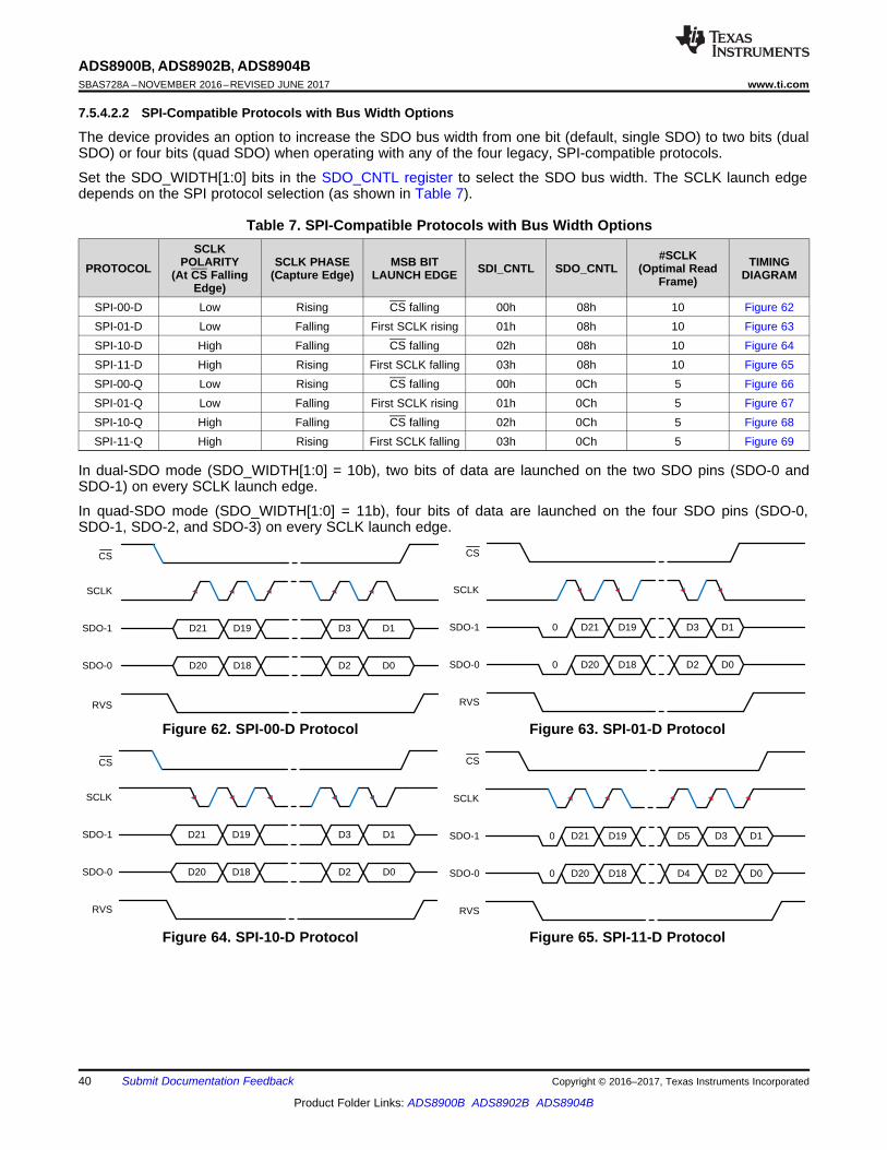
SCLK
SDO-1 D21 D19 D3 D10
CS
D5
SDO-0 D20 D18 D2 D00 D4
RVS
SCLK
SDO-1 D21 D19 D3 D1
CS
SDO-0 D20 D18 D2 D0
RVS
SCLK
SDO-1 D21 D19 D3 D1
CS
SDO-0 D20 D18 D2 D0
RVS
SCLK
SDO-1 0 D21 D19 D3 D1
CS
SDO-0 0 D20 D18 D2 D0
RVS
40
ADS8900B, ADS8902B, ADS8904BSBAS728A –NOVEMBER 2016–REVISED JUNE 2017 www.ti.com
Product Folder Links: ADS8900B ADS8902B ADS8904B
Submit Documentation Feedback Copyright © 2016–2017, Texas Instruments Incorporated
7.5.4.2.2 SPI-Compatible Protocols with Bus Width Options
The device provides an option to increase the SDO bus width from one bit (default, single SDO) to two bits (dualSDO) or four bits (quad SDO) when operating with any of the four legacy, SPI-compatible protocols.
Set the SDO_WIDTH[1:0] bits in the SDO_CNTL register to select the SDO bus width. The SCLK launch edgedepends on the SPI protocol selection (as shown in Table 7).
Table 7. SPI-Compatible Protocols with Bus Width Options
PROTOCOLSCLK
POLARITY(At CS Falling
Edge)
SCLK PHASE(Capture Edge)
MSB BITLAUNCH EDGE SDI_CNTL SDO_CNTL
#SCLK(Optimal Read
Frame)TIMING
DIAGRAM
SPI-00-D Low Rising CS falling 00h 08h 10 Figure 62SPI-01-D Low Falling First SCLK rising 01h 08h 10 Figure 63SPI-10-D High Falling CS falling 02h 08h 10 Figure 64SPI-11-D High Rising First SCLK falling 03h 08h 10 Figure 65SPI-00-Q Low Rising CS falling 00h 0Ch 5 Figure 66SPI-01-Q Low Falling First SCLK rising 01h 0Ch 5 Figure 67SPI-10-Q High Falling CS falling 02h 0Ch 5 Figure 68SPI-11-Q High Rising First SCLK falling 03h 0Ch 5 Figure 69
In dual-SDO mode (SDO_WIDTH[1:0] = 10b), two bits of data are launched on the two SDO pins (SDO-0 andSDO-1) on every SCLK launch edge.
In quad-SDO mode (SDO_WIDTH[1:0] = 11b), four bits of data are launched on the four SDO pins (SDO-0,SDO-1, SDO-2, and SDO-3) on every SCLK launch edge.
Figure 62. SPI-00-D Protocol Figure 63. SPI-01-D Protocol
Figure 64. SPI-10-D Protocol Figure 65. SPI-11-D Protocol
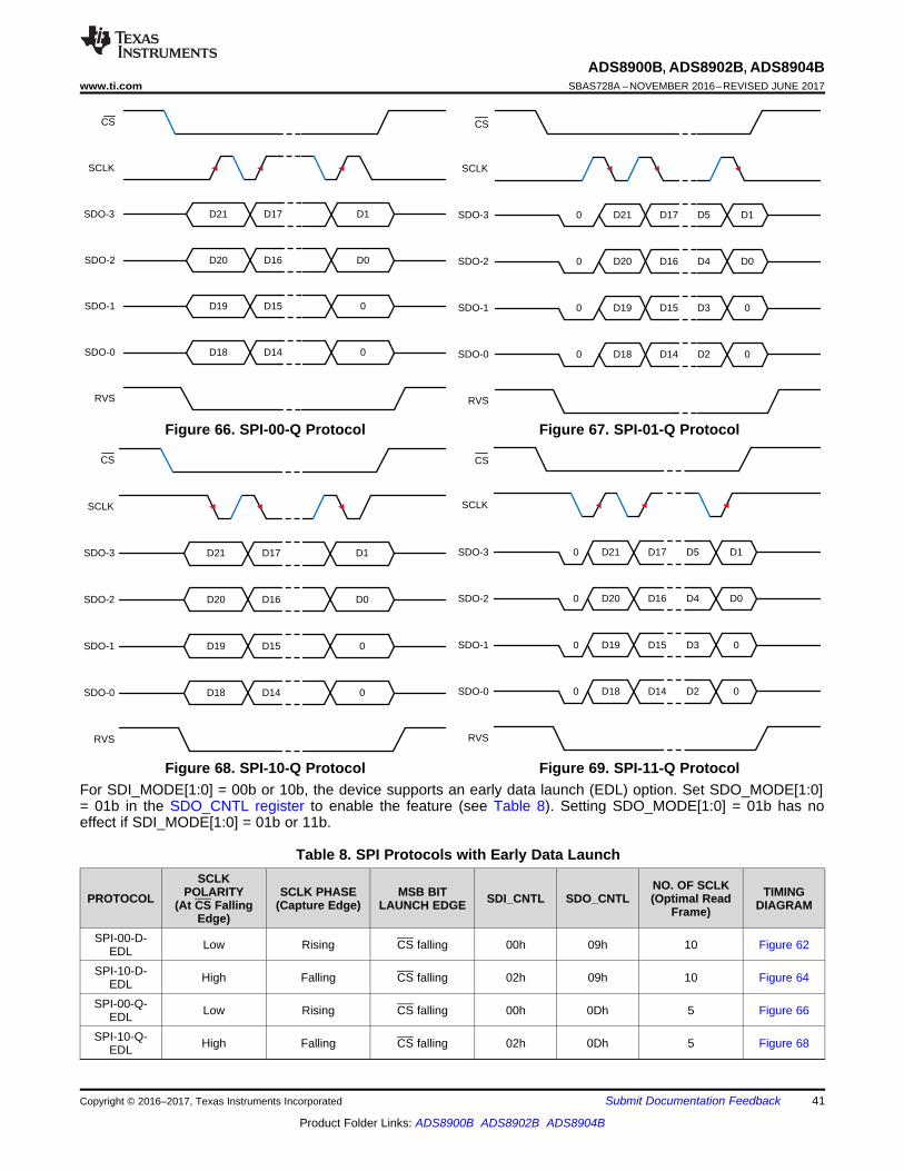
SCLK
SDO-3 D21 D17 D1
CS
SDO-2 D20 D16 D0
SDO-1 D19 D15 0
SDO-0 D18 D14 0
RVS
SCLK
SDO-3 D21 D17 D5 D10
CS
SDO-2
SDO-1
SDO-0
RVS
D20 D16 D4 D00
D19 D15 D3 00
D18 D14 D2 00
SCLK
SDO-3 0 D21 D17 D5 D1
CS
SDO-2
SDO-1
SDO-0
RVS
0 D20 D16 D4 D0
0 D19 D15 D3 0
0 D18 D14 D2 0
SCLK
SDO-3 D21 D17 D1
CS
SDO-2 D20 D16 D0
SDO-1 D19 D15 0
SDO-0 D18 D14 0
RVS
41
ADS8900B, ADS8902B, ADS8904Bwww.ti.com SBAS728A –NOVEMBER 2016–REVISED JUNE 2017
Product Folder Links: ADS8900B ADS8902B ADS8904B
Submit Documentation FeedbackCopyright © 2016–2017, Texas Instruments Incorporated
Figure 66. SPI-00-Q Protocol Figure 67. SPI-01-Q Protocol
Figure 68. SPI-10-Q Protocol Figure 69. SPI-11-Q ProtocolFor SDI_MODE[1:0] = 00b or 10b, the device supports an early data launch (EDL) option. Set SDO_MODE[1:0]= 01b in the SDO_CNTL register to enable the feature (see Table 8). Setting SDO_MODE[1:0] = 01b has noeffect if SDI_MODE[1:0] = 01b or 11b.
Table 8. SPI Protocols with Early Data Launch
PROTOCOLSCLK
POLARITY(At CS Falling
Edge)
SCLK PHASE(Capture Edge)
MSB BITLAUNCH EDGE SDI_CNTL SDO_CNTL
NO. OF SCLK(Optimal Read
Frame)TIMING
DIAGRAM
SPI-00-D-EDL Low Rising CS falling 00h 09h 10 Figure 62
SPI-10-D-EDL High Falling CS falling 02h 09h 10 Figure 64
SPI-00-Q-EDL Low Rising CS falling 00h 0Dh 5 Figure 66
SPI-10-Q-EDL High Falling CS falling 02h 0Dh 5 Figure 68

SCLK
SDO-3 D21 D17 D1
CS
SDO-2 D20 D16 D0
SDO-1 D19 D15 0
SDO-0 D18 D14 0
RVS
SCLK
SDO-3 D21 D17 D1
CS
SDO-2 D20 D16 D0
SDO-1 D19 D15 0
SDO-0 D18 D14 0
RVS
SCLK
SDO-1 D21 D19 D3 D1
CS
SDO-0 D20 D18 D2 D0
RVS
D17
D16
SCLK
SDO-1 D21 D19 D3 D1
CS
SDO-0 D20 D18 D2 D0
RVS
D17
D16
42
ADS8900B, ADS8902B, ADS8904BSBAS728A –NOVEMBER 2016–REVISED JUNE 2017 www.ti.com
Product Folder Links: ADS8900B ADS8902B ADS8904B
Submit Documentation Feedback Copyright © 2016–2017, Texas Instruments Incorporated
As shown in Figure 60, and Figure 61, the device launches the output data bits on the SDO-x pins half clockearlier compared to the standard SPI protocol.
Figure 70. SPI-00-D-EDL Protocol Figure 71. SPI-10-D-EDL Protocol
Figure 72. SPI-00-Q-EDL Protocol Figure 73. SPI-10-Q-EDL Protocol
When using any of the SPI-compatible protocols, the RVS output remains low throughout the data transfer frame;see the Timing Requirements and Switching Characteristics tables for associated timing parameters.
Figure 62 to Figure 73 illustrate how the wider data bus allows the host controller to read all 22 bits of the outputdata word using shorter data transfer frames. Table 7 and Table 8 show the number of SCLK required in anoptimal read frame for the different output protocol selections.
NOTEWith SDO_CNTL[7:0] ≠ 00h or 01h, a long data transfer frame does not result in daisy-chain operation. On SDO pin (or pins), the 22 bits of output data word are followed byzeros.
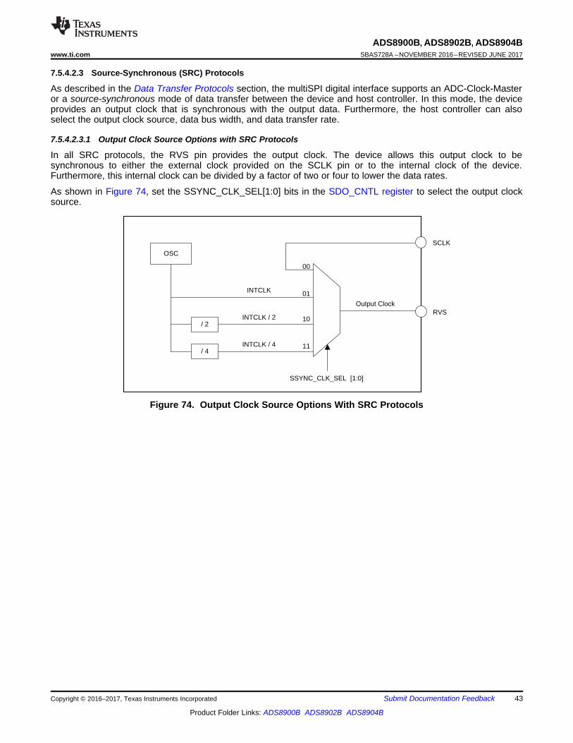
OSC
/ 2
/ 4
INTCLK
INTCLK / 2
INTCLK / 4
01
10
11
00
Output ClockRVS
SCLK
SSYNC_CLK_SEL [1:0]
43
ADS8900B, ADS8902B, ADS8904Bwww.ti.com SBAS728A –NOVEMBER 2016–REVISED JUNE 2017
Product Folder Links: ADS8900B ADS8902B ADS8904B
Submit Documentation FeedbackCopyright © 2016–2017, Texas Instruments Incorporated
7.5.4.2.3 Source-Synchronous (SRC) Protocols
As described in the Data Transfer Protocols section, the multiSPI digital interface supports an ADC-Clock-Masteror a source-synchronous mode of data transfer between the device and host controller. In this mode, the deviceprovides an output clock that is synchronous with the output data. Furthermore, the host controller can alsoselect the output clock source, data bus width, and data transfer rate.
7.5.4.2.3.1 Output Clock Source Options with SRC Protocols
In all SRC protocols, the RVS pin provides the output clock. The device allows this output clock to besynchronous to either the external clock provided on the SCLK pin or to the internal clock of the device.Furthermore, this internal clock can be divided by a factor of two or four to lower the data rates.
As shown in Figure 74, set the SSYNC_CLK_SEL[1:0] bits in the SDO_CNTL register to select the output clocksource.
Figure 74. Output Clock Source Options With SRC Protocols

44
ADS8900B, ADS8902B, ADS8904BSBAS728A –NOVEMBER 2016–REVISED JUNE 2017 www.ti.com
Product Folder Links: ADS8900B ADS8902B ADS8904B
Submit Documentation Feedback Copyright © 2016–2017, Texas Instruments Incorporated
(1) The EXTCLK option is not recommended when operating with DVDD < 2.35 V.(2) Any of the four values can be used; see the Protocols for Configuring the Device section for more information.(3) The device supports INTCLK, INTCLK / 2, and INTCLK / 4 options only for data transfer operations in zone 1. The EXTCLK option is
supported in zone 1 and zone 2; see Figure 46.
7.5.4.2.3.2 Bus Width Options With SRC Protocols
The device provides an option to increase the SDO bus width from one bit (default, single SDO) to two bits (dualSDO) or to four bits (quad SDO) when operating with any of the SRC protocols. Set the SDO_WIDTH[1:0] bits inthe SDO_CNTL register to select the SDO bus width.
In dual-SDO mode (SDO_WIDTH[1:0] = 10b), two bits of data are launched on the two SDO pins (SDO-0 andSDO-1) on every SCLK rising edge.
In quad-SDO mode (SDO_WIDTH[1:0] = 11b), four bits of data are launched on the four SDO pins (SDO-0,SDO-1, SDO-2, and SDO-3) on every SCLK rising edge.
7.5.4.2.3.3 Output Data Rate Options With SRC Protocols
The device provides an option to transfer the data to the host controller at a single data rate (default, SDR) or ata double data rate (DDR). Set the DATA_RATE bit in the SDO_CNTL register to select the data transfer rate.
In SDR mode (DATA_RATE = 0b), the RVS pin toggles from low to high, and the output data bits are launchedon the SDO pins on the output clock rising edge.
In DDR mode (DTA_RATE = 1b), the RVS pin toggles (from low-to-high or high-to-low), and the output data bitsare launched on the SDO pins on every output clock edge, starting with the first rising edge.
The device supports all 24 combinations of output clock source, bus width, and output data rate, as shown inTable 9.
Table 9. SRC Protocol Combinations
PROTOCOL OUTPUT CLOCKSOURCE BUS WIDTH OUTPUT DATA
RATE SDI_CNTL SDO_CNTL#OUTPUT CLOCK
(Optimal ReadFrame)
TIMINGDIAGRAM
SRC-EXT-SS SCLK (1) Single SDR
00h, 01h,02h, or 03h (2)
03h 10 Figure 75
SRC-INT-SS INTCLK (3) Single SDR 43h 10
Figure 76SRC-IB2-SS INTCLK / 2 (3) Single SDR 83h 10
SRC-IB4-SS INTCLK / 4 (3) Single SDR C3h 10
SRC-EXT-DS SCLK (1) Dual SDR 0Bh 10 Figure 79
SRC-INT-DS INTCLK (3) Dual SDR 4Bh 10
Figure 80SRC-IB2-DS INTCLK / 2 (3) Dual SDR 8Bh 10
SRC-IB4-DS INTCLK / 4 (3) Dual SDR CBh 10
SRC-EXT-QS SCLK (1) Quad SDR 0Fh 5 Figure 83
SRC-INT-QS INTCLK (3) Quad SDR 4Fh 5
Figure 84SRC-IB2-QS INTCLK / 2 (3) Quad SDR 8Fh 5
SRC-IB4-QS INTCLK / 4 (3) Quad SDR CFh 5
SRC-EXT-SD SCLK (1) Single DDR 13h 10 Figure 77
SRC-INT-SD INTCLK (3) Single DDR 53h 10
Figure 78SRC-IB2-SD INTCLK / 2 (3) Single DDR 93h 10
SRC-IB4-SD INTCLK / 4 (3) Single DDR D3h 10
SRC-EXT-DD SCLK (1) Dual DDR 1Bh 5 Figure 81
SRC-INT-DD INTCLK (3) Dual DDR 5Bh 5
Figure 82SRC-IB2-DD INTCLK / 2 (3) Dual DDR 9Bh 5
SRC-IB4-DD INTCLK / 4 (3) Dual DDR DBh 5
SRC-EXT-QD SCLK (1) Quad DDR 1Fh 3 Figure 85
SRC-INT-QD INTCLK (3) Quad DDR 5Fh 3
Figure 86SRC-IB2-QD INTCLK / 2 (3) Quad DDR 9Fh 3
SRC-IB4-QD INTCLK / 4 (3) Quad DDR DFh 3

SCLK
SDO-1 D21 D19 D3 D1
CS
RVS
D5
SDO-0 D20 D18 D2 D0D4
SCLK
SDO-1 D21 D19 D3 D1
CS
RVS
D5
SDO-0 D20 D18 D2 D0D4
SCLK
SDO-0
D21
D20
CS
RVS
D19
D21 D20
D1
D0D2
D1D2D3 D0
SCLK
SDO-0
CS
RVS
D21 D20 D1D2D3 D0
SCLK
SDO-0 D21 D20 D1 D0
D21 D20 D0
CS
RVS
D19 D1
D2
SCLK
SDO-0 D21 D20 D1 D0
CS
RVS
D2
45
ADS8900B, ADS8902B, ADS8904Bwww.ti.com SBAS728A –NOVEMBER 2016–REVISED JUNE 2017
Product Folder Links: ADS8900B ADS8902B ADS8904B
Submit Documentation FeedbackCopyright © 2016–2017, Texas Instruments Incorporated
Figure 75 to Figure 86 show the details of various source synchronous protocols. Table 9 shows the number ofoutput clocks required in an optimal read frame for the different output protocol selections.
Figure 75. SRC-EXT-SS: SRC, SCLK, Single SDO,SDR
Figure 76. SRC-INT-SS: SRC, INTCLK, Single SDO,SDR
Figure 77. SRC-EXT-SD: SRC, SCLK, Single SDO,DDR
Figure 78. SRC-INT-SD: SRC, INTCLK, Single SDO,DDR
Figure 79. SRC-EXT-DS: SRC, SCLK, Dual SDO,SDR
Figure 80. SRC-INT-DS: SRC, INTCLK, Dual SDO,SDR

SCLK
SDO-3
CS
RVS
D21 D17 D9D13
SDO-2 D20 D16 D8D12
SDO-1 D19 D15 D7D11
SDO-0 D18 D14 D6D10
D5
D4
D3
D2
D1
D0
0
0
SCLK
SDO-3
CS
RVS
D21 D17 D9D13
SDO-2 D20 D16 D8D12
SDO-1 D19 D15 D7D11
SDO-0 D18 D14 D6D10
D5
D4
D3
D2
D1
D0
0
0
SCLK
SDO-3 D21 D17 D5
CS
RVS
D13
SDO-2 D20 D16 D8 D4D12
SDO-1 D19 D15 D7 D3D11
SDO-0 D18 D14 D6 D2D10
D9 D1
D0
0
0
SCLK
SDO-3 D21 D17 D5
CS
RVS
D13
SDO-2 D20 D16 D8 D4D12
SDO-1 D19 D15 D7 D3D11
SDO-0 D18 D14 D6 D2D10
D9 D1
D0
0
0
SCLK
SDO-1
CS
RVS
D21 D19 D3D5D7 D1
SDO-0 D20 D18 D2D4D6 D0
SCLK
SDO-1
CS
RVS
D21 D19 D3D5D7 D1
SDO-0 D20 D18 D2D4D6 D0
46
ADS8900B, ADS8902B, ADS8904BSBAS728A –NOVEMBER 2016–REVISED JUNE 2017 www.ti.com
Product Folder Links: ADS8900B ADS8902B ADS8904B
Submit Documentation Feedback Copyright © 2016–2017, Texas Instruments Incorporated
Figure 81. SRC-EXT-DD: SRC, SCLK, Dual SDO,DDR
Figure 82. SRC-INT-DD: SRC, INTCLK, Dual SDO,DDR
Figure 83. SRC-EXT-QS: SRC, SCLK, Quad SDO,SDR
Figure 84. SRC-INT-QS: SRC, INTCLK, Quad SDO,SDR
Figure 85. SRC-EXT-QD: SRC, SCLK, Quad SDO,DDR
Figure 86. SRC-INT-QD: SRC, INTCLK, Quad SDO,DDR

DVDD
(Optional)
(Optional)
(Optional)CONVST
SCLK
SDI
RST
CS
SDO-0Host
Controller
(Optional)Isolation
TI Device
SDO-1
SDO-2
SDO-3
RVS
Copyright © 2016, Texas Instruments Incorporated
CONVST
SCLK
SDI
RST
CS
SDO-0Host
Controller
(Optional)Isolation
DVDD
TI Device
SDO-1
SDO-2
SDO-3
RVS
Copyright © 2016, Texas Instruments Incorporated
47
ADS8900B, ADS8902B, ADS8904Bwww.ti.com SBAS728A –NOVEMBER 2016–REVISED JUNE 2017
Product Folder Links: ADS8900B ADS8902B ADS8904B
Submit Documentation FeedbackCopyright © 2016–2017, Texas Instruments Incorporated
7.5.5 Device SetupThe multiSPI digital interface and the device configuration registers offer multiple operation modes. This sectiondescribes how to select the hardware connection topology to meet different system requirements.
7.5.5.1 Single Device: All multiSPI OptionsFigure 87 shows the connections between a host controller and a single device in order to exercise all optionsprovided by the multiSPI digital interface.
Figure 87. MultiSPI Digital Interface, All Pins
7.5.5.2 Single Device: Minimum Pins for a Standard SPI InterfaceFigure 88 shows the minimum-pin interface for applications using a standard SPI protocol.
Figure 88. SPI Interface, Minimum Pins
The CS, SCLK, SDI, and SDO-0 pins constitute a standard SPI port of the host controller. The CONVST pin istied to CS, and the RST pin is tied to DVDD. The SDO-1, SDO-2, and SDO-3 pins have no external connections.The following features are also available:• Control the CONVST pin independently to get additional timing flexibility.• Control RST pin independently to add asynchronous reset functionality.• Monitor the RVS pin for additional timing benefits.

Unified Shift Register (USR)
22 Bits
DB0
DB1
DB 20
DB 21
Device 1
SDI SDO-0
Unified Shift Register (USR)
22 Bits
DB0
DB1
DB20
DB21
Device 2
SDI SDO-0
Unified Shift Register (USR)
22 Bits
DB0
DB1
DB20
DB21
Device N
SDI SDO-0
Host Controller
CONVST SCLKSDO SDICS
CO
NV
ST
SC
LK SD
I
CS
SD
O-0
RV
S
Device 1
CO
NV
ST
SC
LK SD
I
CS
SD
O-0
RV
S
CO
NV
ST
SC
LK SD
I
CS
SD
O-0
RV
S
Device 2 Device N
Isol
atio
n
Host ControllerC
ON
VS
T
CS
SC
LK
SD
O
SD
I
(Opt
iona
l)
48
ADS8900B, ADS8902B, ADS8904BSBAS728A –NOVEMBER 2016–REVISED JUNE 2017 www.ti.com
Product Folder Links: ADS8900B ADS8902B ADS8904B
Submit Documentation Feedback Copyright © 2016–2017, Texas Instruments Incorporated
7.5.5.3 Multiple Devices: Daisy-Chain TopologyA typical connection diagram showing multiple devices in a daisy-chain topology is shown in Figure 89.
Figure 89. Daisy-Chain Connections
The CONVST, CS, and SCLK inputs of all devices are connected together and controlled by a single CONVST,CS, and SCLK pin of the host controller, respectively. The SDI input pin of the first device in the chain (Device 1)is connected to the SDO pin of the host controller, the SDO-0 output pin of Device 1 is connected to the SDIinput pin of Device 2, and so on. The SDO-0 output pin of the last device in the chain (Device N) is connected tothe SDI pin of the host controller.
To operate multiple devices in a daisy-chain topology, the host controller sets the configuration registers in eachdevice with identical values and operates with any of the legacy, SPI-compatible protocols for data-read anddata-write operations (SDO_CNT[7:0] = 00h or 01h). With these configurations settings, the 22-bit ODR and 22-bit IDR registers in each device collapse to form a single, 22-bit unified shift register (USR) per device, as shownin Figure 90.
Figure 90. Unified Shift Register

SCLK
{SDO-0}1
{SDI}2{D21}1
CS
{SDO}HOST
{SDI}1B44B45B65 B64 B43 B42
{D1}1 B65 B64
B22B23 B21 B20
B45 B44 B43 B42
B0B1
B23 B22{D20}1 {D0}1
{SDO-0}2
{SDI}3{D21}2 {D1}2 B65 B64 B45 B44{D20}2 {D0}2 {D21}1 {D20}1 {D1}1 {D0}1
{SDO-0}3
{SDI}HOST{D21}3 {D1}3{D20}3 {D0}3 {D21}2 {D20}2 {D1}2 {D0}2 {D21}1 {D20}1 {D1}1 {D0}1
1 2 21 22 23 24 43 44 45 46 65 66
Configuration Data Device 1
Configuration Data Device 2
Configuration Data Device 3
Output Data ± Device 3 Output Data ± Device 2 Output Data ± Device 1
49
ADS8900B, ADS8902B, ADS8904Bwww.ti.com SBAS728A –NOVEMBER 2016–REVISED JUNE 2017
Product Folder Links: ADS8900B ADS8902B ADS8904B
Submit Documentation FeedbackCopyright © 2016–2017, Texas Instruments Incorporated
All devices in the daisy-chain topology sample the respective device analog input signals on the CONVST risingedge. The data transfer frame starts with a CS falling edge. On each SCLK launch edge, every device in thechain shifts out the MSB of the respective USR on to the respective SDO-0 pin. On every SCLK capture edge,each device in the chain shifts in data received on the respective SDI pin as the LSB bit of the respective USR.Therefore, in a daisy-chain configuration, the host controller receives the data of Device N, followed by the dataof Device N – 1, and so on (MSB-first). On the CS rising edge, each device decodes the contents in therespective USR, and takes appropriate action.
A typical timing diagram for three devices connected in daisy-chain topology using the SPI-00-S protocol isshown in Figure 91.
Figure 91. Three-Device, Daisy-Chain Timing
In daisy-chain topology, the overall throughput of the system is proportionally reduced as more devices areconnected in the daisy-chain.
NOTEFor N devices connected in daisy-chain topology, an optimal data transfer frame mustcontain 22 × N SCLK capture edges. For a longer data transfer frame (number of SCLK inthe frame > 22 × N), the host controller must appropriately align the configuration data foreach device before bringing CS high. A shorter data transfer frame (number of SCLK inthe frame < 22 × N) might result in an erroneous device configuration, and must beavoided.
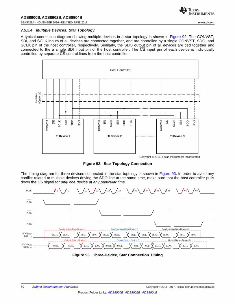
SCLK
{CS}1
{SDO}HOST
{SDI}1,2,3{B21}1
{SDO-0}1,2,3
{SDI}HOST{D21}1 {D1}1{D20}1 {D0}1 {D21}2 {D20}2 {D1}2 {D0}2 {D21}3 {D20}3 {D1}3 {D0}3
1 2 21 22 23 24 43 44 45 46 65 66
Configuration Data Device 1 Configuration Data Device 2 Configuration Data Device 3
Output Data ± Device 1 Output Data ± Device 2 Output Data ± Device 3
{CS}2
{CS}3
{B20}1 {B1}1 {B0}1 {B21}2 {B20}2 {B1}2 {B0}2 {B21}3 {B20}3 {B1}3 {B0}3
Host Controller
TI Device 1
CO
NV
ST
SC
LK SD
I
CS
SD
O
TI Device 2
RV
S
CO
NV
ST
SC
LK
SD
I
CS
SD
O
RV
S
TI Device N
CO
NV
ST
SC
LK
SD
I
CS
SD
O
RV
S
Isol
atio
n(O
ptio
nal)
Copyright © 2016, Texas Instruments Incorporated
50
ADS8900B, ADS8902B, ADS8904BSBAS728A –NOVEMBER 2016–REVISED JUNE 2017 www.ti.com
Product Folder Links: ADS8900B ADS8902B ADS8904B
Submit Documentation Feedback Copyright © 2016–2017, Texas Instruments Incorporated
7.5.5.4 Multiple Devices: Star TopologyA typical connection diagram showing multiple devices in a star topology is shown in Figure 92. The CONVST,SDI, and SCLK inputs of all devices are connected together, and are controlled by a single CONVST, SDO, andSCLK pin of the host controller, respectively. Similarly, the SDO output pin of all devices are tied together andconnected to the a single SDI input pin of the host controller. The CS input pin of each device is individuallycontrolled by separate CS control lines from the host controller.
Figure 92. Star-Topology Connection
The timing diagram for three devices connected in the star topology is shown in Figure 93. In order to avoid anyconflict related to multiple devices driving the SDO line at the same time, make sure that the host controller pullsdown the CS signal for only one device at any particular time.
Figure 93. Three-Device, Star Connection Timing

51
ADS8900B, ADS8902B, ADS8904Bwww.ti.com SBAS728A –NOVEMBER 2016–REVISED JUNE 2017
Product Folder Links: ADS8900B ADS8902B ADS8904B
Submit Documentation FeedbackCopyright © 2016–2017, Texas Instruments Incorporated
7.6 Register Maps
7.6.1 Device Configuration and Register MapsThe device features nine configuration registers, mapped as described in Table 10.
Table 10. Configuration Registers MappingADDRESS REGISTER NAME REGISTER DESCRIPTION
004h PD_CNTL Low-power modes control008h SDI_CNTL SDI input protocol selection00Ch SDO_CNTL SDO output protocol selection010h DATA_CNTL Output data word configuration014h PATN_LSB Eight least significant bits (LSB) of the output pattern015h PATN_MID Eight middle bits of the output pattern016h PATN_MSB Four most significant bits (MSB) of the output pattern020h OFST_CAL Offset calibration030h REF_MRG Reference margin
7.6.1.1 PD_CNTL Register (address = 04h) [reset = 00h]This register controls the low-power modes offered by the device.
Figure 94. PD_CNTL Register
7 6 5 4 3 2 1 00 0 0 0 0 PD_REFBUF PD_ADC 0
R-0b R-0b R-0b R-0b R-0b R/W-0b R/W-0b R-0bLEGEND: R/W = Read/Write; R = Read only; -n = value after reset
Table 11. PD_CNTL Register Field DescriptionsBit Field Type Reset Description7-3 0 R 00000b Reserved bits. Reads return 00000b.2 PD_REFBUF R/W 0b This bit powers down the internal reference buffer.
0b = Internal reference buffer is powered up1b = Internal reference buffer is powered down
1 PD_ADC R/W 0b This bit powers down the converter module.0b = converter module is powered up1b = converter module is powered down
0 0 R 0b Reserved bits. Do not write. Reads return 0b.
To power-down the converter module, set the PD_ADC bit in the PD_CNTL register. The converter modulepowers down on the rising edge of CS. To power-up the converter module, reset the PD_ADC bit in thePD_CNTL register. The converter module starts to power-up on the rising edge of CS. Wait for tPU_ADC beforeinitiating any conversion or data transfer operation.
To power-down the internal reference buffer, set the PD_REFBUF bit in the PD_CNTL register. The internalreference buffer powers down on the rising edge of CS. To power-up the internal reference buffer, reset thePD_REFBUF bit in the PD_CNTL register. The internal reference buffer starts to power-up on the rising edge ofCS. Wait for tPU_REFBUF before initiating any conversion.

52
ADS8900B, ADS8902B, ADS8904BSBAS728A –NOVEMBER 2016–REVISED JUNE 2017 www.ti.com
Product Folder Links: ADS8900B ADS8902B ADS8904B
Submit Documentation Feedback Copyright © 2016–2017, Texas Instruments Incorporated
7.6.1.2 SDI_CNTL Register (address = 008h) [reset = 00h]This register selects the SPI protocol for writing data to the device.
Figure 95. SDI_CNTL Register
7 6 5 4 3 2 1 00 0 0 0 0 0 SDI_MODE[1:0]
R-0b R-0b R-0b R-0b R-0b R-0b R/W-00bLEGEND: R/W = Read/Write; R = Read only; -n = value after reset
Table 12. SDI_CNTL Register Field DescriptionsBit Field Type Reset Description7-2 0 R 000000b Reserved bits. Do not write. Reads return 000000b.1-0 SDI_MODE[1:0] R/W 00b These bits select the protocol for writing data into the device.
00b = Standard SPI with CPOL = 0 and CPHASE = 001b = Standard SPI with CPOL = 0 and CPHASE = 110b = Standard SPI with CPOL = 1 and CPHASE = 011b = Standard SPI with CPOL = 1 and CPHASE = 1
7.6.1.3 SDO_CNTL Register (address = 0Ch) [reset = 00h]This register configures the protocol for reading data from the device.
Figure 96. SDO_CNTL Register
7 6 5 4 3 2 1 0SSYNC_CLK_SEL[1:0] 0 DATA_RATE SDO_WIDTH[1:0] SDO_MODE[1:0]
R/W-00b R-0b R/W-0b R/W-00b R/W-00bLEGEND: R/W = Read/Write; R = Read only; -n = value after reset
Table 13. SDO_CNTL Register Field DescriptionsBit Field Type Reset Description7-6 SSYNC_CLK_SEL[1:0] R/W 00b These bits select the source and frequency of the clock for the ADC-
Clock-Master mode, and are valid only if SDO_MODE[1:0] = 11b.00b = External SCLK echo01b = Internal clock (INTCLK)10b = Internal clock / 2 (INTCLK / 2)11b = Internal clock / 4 (INTCLK / 4)
5 0 R 0b Reserved bit. Do not write. Reads return 0b.4 DATA_RATE R/W 0b This bit is ignored if SDO_MODE[1:0] = 00b. When SDO_MODE[1:0] =
11b:0b = SDOs are updated at single data rate (SDR) with respect to theoutput clock1b = SDOs are updated at double data rate (DDR) with respect to theoutput clock
3-2 SDO_WIDTH[1:0] R/W 00b These bits set the width of the output bus.0xb = Data are output only on SDO-010b = Data are output only on SDO-0 and SDO-111b = Data are output on SDO-0, SDO-1, SDO-2, and SDO-3
1-0 SDO_MODE[1:0] R/W 00b These bits select the protocol for reading data from the device.00b = SDO follows the SPI protocol selected in the SDI_CNTL register01b = SDO follows the SPI protocol selected in the SDI_CNTL registerbut with Early Data Launch feature enabled. See Table 6.10b = Invalid configuration, not supported by the device11b = SDO follows the source-synchronous protocol

53
ADS8900B, ADS8902B, ADS8904Bwww.ti.com SBAS728A –NOVEMBER 2016–REVISED JUNE 2017
Product Folder Links: ADS8900B ADS8902B ADS8904B
Submit Documentation FeedbackCopyright © 2016–2017, Texas Instruments Incorporated
7.6.1.4 DATA_CNTL Register (address = 010h) [reset = 00h]This register configures the contents of the 22-bit output data word (D[21:0]).
Figure 97. DATA_CNTL Register
7 6 5 4 3 2 1 00 0 0 0 FPAR_LOC[1:0] PAR_EN DATA_VAL
R-0b R-0b R-0b R-0b R/W-00b R/W-0b R/W-0bLEGEND: R/W = Read/Write; R = Read only; -n = value after reset
Table 14. DATA_CNTL Register Field DescriptionsBit Field Type Reset Description7-4 0 R 0000b Reserved bits. Reads return 0000b.3-2 FPAR_LOC[1:0] R/W 00b These bits control the data span for calculating the FTPAR bit (bit D[0] in
the output data word).00b = D[0] reflects even parity calculated for 4 MSB01b = D[0] reflects even parity calculated for 8 MSB10b = D[0] reflects even parity calculated for 12 MSB11b = D[0] reflects even parity calculated for 16 MSB
1 PAR_EN R/W 0b 0b = Output data does not contain any parity informationD[1] = 0D[0] = 0
1b = Parity information is appended to the LSB of the output dataD[1] = Even parity calculated on bits D[21:2]D[0] = Even parity computed on selected number of MSB of D[21:2] as
per FPAR_LOC[1:0] settingSee Figure 44 for further details of parity computation.
0 DATA_VAL R/W 0b These bits control bits D[21:2] of the output data word.0b = 20-bit conversion output1b = 20-bit contents of the fixed-pattern registersSee PATN CNTL for more details.
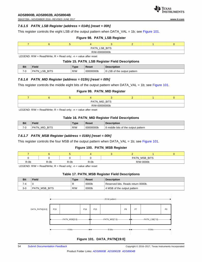
P19DATA_PATN[19:0] P16 P15 P8 P7 P0
PATN_MSB[3:0] PATN_MID[7:0] PATN_LSB[7:0]
20-bit pattern
4-bits 8-bits 8-bits
54
ADS8900B, ADS8902B, ADS8904BSBAS728A –NOVEMBER 2016–REVISED JUNE 2017 www.ti.com
Product Folder Links: ADS8900B ADS8902B ADS8904B
Submit Documentation Feedback Copyright © 2016–2017, Texas Instruments Incorporated
7.6.1.5 PATN_LSB Register (address = 014h) [reset = 00h]This register controls the eight LSB of the output pattern when DATA_VAL = 1b; see Figure 101.
Figure 98. PATN_LSB Register
7 6 5 4 3 2 1 0PATN_LSB_BITSR/W-00000000b
LEGEND: R/W = Read/Write; R = Read only; -n = value after reset
Table 15. PATN_LSB Register Field DescriptionsBit Field Type Reset Description7-0 PATN_LSB_BITS R/W 00000000b 8 LSB of the output pattern
7.6.1.6 PATN_MID Register (address = 015h) [reset = 00h]This register controls the middle eight bits of the output pattern when DATA_VAL = 1b; see Figure 101.
Figure 99. PATN_MID Register
7 6 5 4 3 2 1 0PATN_MID_BITSR/W-00000000b
LEGEND: R/W = Read/Write; R = Read only; -n = value after reset
Table 16. PATN_MID Register Field DescriptionsBit Field Type Reset Description7-0 PATN_MID_BITS R/W 00000000b 8 middle bits of the output pattern
7.6.1.7 PATN_MSB Register (address = 016h) [reset = 00h]This register controls the four MSB of the output pattern when DATA_VAL = 1b; see Figure 101.
Figure 100. PATN_MSB Register
7 6 5 4 3 2 1 00 0 0 0 PATN_MSB_BITS
R-0b R-0b R-0b R-0b R/W-0000bLEGEND: R/W = Read/Write; R = Read only; -n = value after reset
Table 17. PATN_MSB Register Field DescriptionsBit Field Type Reset Description7-4 0 R 0000b Reserved bits. Reads return 0000b.3-0 PATN_MSB_BITS R/W 0000b 4 MSB of the output pattern
Figure 101. DATA_PATN[19:0]

55
ADS8900B, ADS8902B, ADS8904Bwww.ti.com SBAS728A –NOVEMBER 2016–REVISED JUNE 2017
Product Folder Links: ADS8900B ADS8902B ADS8904B
Submit Documentation FeedbackCopyright © 2016–2017, Texas Instruments Incorporated
7.6.1.8 OFST_CAL Register (address = 020h) [reset = 00h]This register selects the external reference range for optimal offset calibration.
Figure 102. OFST_CAL Register
7 6 5 4 3 2 1 00 0 0 0 0 REF_SEL[2:0]
R-0b R-0b R-0b R-0b R-0b R/W-000bLEGEND: R/W = Read/Write; R = Read only; -n = value after reset
Table 18. OFST_CAL Register Field DescriptionsBit Field Type Reset Description7-3 0 R 00000b Reserved bits. Reads return 00000b.2-0 REF_SEL[2:0] R/W 000b These bits select the external reference range for optimal offset.
000b = Optimum offset calibration for VREF = 5.0 V001b = Optimum offset calibration for VREF = 4.5 V010b = Optimum offset calibration for VREF = 4.096 V011b = Optimum offset calibration for VREF = 3.3 V100b = Optimum offset calibration for VREF = 3.0 V101b = Optimum offset calibration for VREF = 2.5 V110b = Optimum offset calibration for VREF = 5.0 V111b = Optimum offset calibration for VREF = 5.0 V

56
ADS8900B, ADS8902B, ADS8904BSBAS728A –NOVEMBER 2016–REVISED JUNE 2017 www.ti.com
Product Folder Links: ADS8900B ADS8902B ADS8904B
Submit Documentation Feedback Copyright © 2016–2017, Texas Instruments Incorporated
7.6.1.9 REF_MRG Register (address = 030h) [reset = 00h]This register selects the margining to be added to or subtracted from the reference buffer output; see theReference Buffer Module section.
Figure 103. REF_MRG Register
7 6 5 4 3 2 1 00 0 EN_MARG REF_OFST[4:0]
R-0b R-0b R/W-0b R/W-00000bLEGEND: R/W = Read/Write; R = Read only; -n = value after reset
Table 19. REF_MRG Register Field DescriptionsBit Field Type Reset Description7-6 0 R 00b Reserved bits. Reads return 00b.5 EN_MARG R/W 0b This bit enables margining feature.
0b = Margining is disabled1b = Margining is enabled
4-0 REF_OFST[4:0] R/W 00000b These bits select the reference offset value as per Table 20.
(1) The actual VREFBUFOUT value may vary by ±10% from Table 20
Table 20. REF_OFST[4:0] settings
REF_OFST[4:0] ΔVREFBUFOUT (typical (1))
00000b 0 mV
00001b 280 µV
00010b 580 µV
00011b 840 µV
00100b 1.12 mV
00101b 1.4 mV
00110b 1.68 mV
00111b 1.96 mV
01000b 2.24 mV
01001b 2.52 mV
01010b 2.8 mV
01011b 3.08 mV
01100b 3.36 mV
01101b 3.64 mV
01110b 3.92 mV
01111b 4.2 mV
10000b –4.5 mV
10001b –4.22 mV
10010b –3.94 mV
10011b –3.66 mV
10100b –3.38 mV
10101b –3.1 mV
10110b –2.82 mV
10111b –2.54 mV
11000b –2.26 mV
11001b –1.98 mV
11010b –1.7 mV
11011b –1.42 mV
11100b –1.14 mV
11101b –860 µV
11110b –580 µV
11111b –280 µV

ADS89xxB
RFLT
2.2
RFLT
2.2
CFLT
10 nF
CFLT
10 nF
57
ADS8900B, ADS8902B, ADS8904Bwww.ti.com SBAS728A –NOVEMBER 2016–REVISED JUNE 2017
Product Folder Links: ADS8900B ADS8902B ADS8904B
Submit Documentation FeedbackCopyright © 2016–2017, Texas Instruments Incorporated
8 Application and Implementation
NOTEInformation in the following applications sections is not part of the TI componentspecification, and TI does not warrant its accuracy or completeness. TI’s customers areresponsible for determining suitability of components for their purposes. Customers shouldvalidate and test their design implementation to confirm system functionality.
8.1 Application InformationThe two primary circuits required to maximize the performance of a high-precision, successive approximationregister (SAR), analog-to-digital converter (ADC) are the input driver and the reference driver circuits. Thissection presents general principles for designing these circuits, followed by an application circuit designed usingthe ADS890xB.
8.1.1 ADC Reference DriverThe external reference source must provide low-drift and very accurate voltage at the REFIN pin of theADS890xB. The output broadband noise of most references can be in the order of a few hundred μVRMS.Therefore, to prevent any degradation in the noise performance of the ADC, appropriately filter the output of thevoltage reference by using a low-pass filter with a cutoff frequency of a few hundred hertz.
The internal reference buffer of the ADS890xB provides the dynamic load posed on the REFBUFOUT pin duringthe conversion process. Decouple the REFBUFOUT pin with the REFM pin using the recommended CREFBUF andRESR. See the Layout section for layout recommendations.
8.1.2 ADC Input DriverThe input driver circuit for a high-precision ADC mainly consists of two parts: a driving amplifier and a chargekickback filter. The amplifier is used for signal conditioning of the input signal and the low output impedance ofthe amplifier provides a buffer between the signal source and the switched capacitor inputs of the ADC. Thecharge kickback filter helps attenuate the sampling charge injection from the switched-capacitor input stage ofthe ADC, and band-limits the wideband noise contributed by the front-end circuit. Careful design of the front-endcircuit is critical to meet the linearity and noise performance of the ADS890xB.
8.1.2.1 Charge-Kickback FilterThe charge-kickback filter is an RC filter at the input pins of the ADC that filters the broadband noise from thefront-end drive circuitry, and attenuates the sampling charge injection from the switched-capacitor input stage ofthe ADC. A filter capacitor, CFLT, is connected from each input pin of the ADC to the ground (as shown inFigure 104). This capacitor helps reduce the sampling charge injection and provides a charge bucket to quicklycharge the internal sample-and-hold capacitors during the acquisition process. Generally, the value of thiscapacitor must be at least 20 times the specified value of the ADC sampling capacitance. For the ADS890xB, theinput sampling capacitance is equal to 60 pF; therefore, for optimal performance, keep CFLT greater than 1.2 nF.This capacitor must be a COG- or NPO-type. The type of dielectric used in COG or NPO ceramic capacitorsprovides the most stable electrical properties over voltage, frequency, and temperature changes.
Figure 104. Charge Kickback Filter Configuration

� �¸¹
ᬩ
§�
� uuduS
u�¸̧¸
¹
·
¨̈¨
©
§uu 20
dBSNR
REFdB3
2RMS_n
2
PP_AMP_f1
G 102
V51
f2
e6.6
V2N
� �dB10THDTHD ADCAMP �d
FLT FLT
1UGB 4
2 R CS
§ ·t u ¨ ¸
u u© ¹
58
ADS8900B, ADS8902B, ADS8904BSBAS728A –NOVEMBER 2016–REVISED JUNE 2017 www.ti.com
Product Folder Links: ADS8900B ADS8902B ADS8904B
Submit Documentation Feedback Copyright © 2016–2017, Texas Instruments Incorporated
Application Information (continued)Driving capacitive loads can degrade the phase margin of the input amplifier, thus making the amplifiermarginally unstable. To avoid amplifier stability issues, series isolation resistors (RFLT) are used at the output ofthe amplifiers. A higher value of RFLT helps with amplifier stability, but adds distortion as a result of interactionswith the nonlinear input impedance of the ADC. Distortion increases with source impedance, input signalfrequency, and input signal amplitude. Therefore, the selection of RFLT requires balancing the stability of thedriver amplifier and distortion performance of the design. Always verify the stability and settling behavior of thedriving amplifier and charge-kickback filter by TINA-TI™ SPICE simulation. Keep the tolerance of the selectedresistors less than 1% to keep the inputs balanced.
8.1.2.2 Input Amplifier SelectionSelection criteria for the input amplifiers is highly dependent on the input signal type, as well as the performancegoals, of the data acquisition system. Some key amplifier specifications to consider when selecting anappropriate amplifier to drive the inputs of the ADC are:• Small-signal bandwidth. Select the small-signal bandwidth of the input amplifiers to be as high as possible
after meeting the power budget of the system. Higher bandwidth reduces the closed-loop output impedanceof the amplifier, thus allowing the amplifier to more easily drive the ADC sample-and-hold capacitor and theRC filter (Charge-Kickback Filter) at the inputs of the ADC. Higher bandwidth amplifiers offer faster settlingtimes while driving the capacitive load of the charge-kickback filter, thus reducing harmonic distortion athigher input frequencies. In order to maintain the overall stability of the input driver circuit, select the amplifierwith a unity gain bandwidth (UGB) as described in Equation 16:
(16)• Distortion. Both the ADC and the input driver introduce distortion in a data acquisition block. To make sure
that the distortion performance of the data acquisition system is not limited by the front-end circuit, thedistortion of the input driver must be at least 10 dB less than the distortion of the ADC, as shown inEquation 17.
(17)• Noise. Noise contribution of the front-end amplifiers must be as low as possible to prevent any degradation in
SNR performance of the system. Generally, to make sure that the noise performance of the data acquisitionsystem is not limited by the front-end circuit, the total noise contribution from the front-end circuit must bekept below 20% of the input-referred noise of the ADC. Noise from the input driver circuit is band-limited bydesigning a low cutoff frequency, charge-kickback filter, as explained in Equation 18.
where:• V1 / f_AMP_PP is the peak-to-peak flicker noise in µV• en_RMS is the amplifier broadband noise density in nV/√Hz• f–3dB is the 3-dB bandwidth of the charge-kickback filter• NG is the noise gain of the front-end circuit that is equal to 1 in a buffer configuration (18)
• Settling Time. For dc signals with fast transients that are common in a multiplexed application, the input signalmust settle within an 20-bit accuracy at the device inputs during the acquisition time window. This condition iscritical to maintain the overall linearity performance of the ADC. Typically, amplifier data sheets specify theoutput settling performance only up to 0.1% to 0.001%, which may not be sufficient for the desired 20-bitaccuracy. Therefore, always verify the settling behavior of the input driver by TINA-TI SPICE simulationsbefore selecting the amplifier.

ADS89xxB
ADC
DECAP
BUF
5 VRVDD
REFIN REFBUFOUT
REFM
GND
REF5045
VIN VOUT
GND
OPA2625
5 V
VCM 1.12 V
5 V
LDO
1 �F 0.1
10 �F
10 �F
1 k
1 �F
1 �F
0.1
22 �F
1 nF
1 k
1 k 2.2
10 nF
10 nF
2.2 1 k
1 k
1 nF
59
ADS8900B, ADS8902B, ADS8904Bwww.ti.com SBAS728A –NOVEMBER 2016–REVISED JUNE 2017
Product Folder Links: ADS8900B ADS8902B ADS8904B
Submit Documentation FeedbackCopyright © 2016–2017, Texas Instruments Incorporated
8.2 Typical Application
8.2.1 Data Acquisition (DAQ) Circuit for Lowest Distortion and Noise Performance With Differential Input
Figure 105. Differential-Input DAQ Circuit for Lowest Distortion and Noise Using the ADS890xB
8.2.1.1 Design RequirementsFor this example, the design parameters are listed in Table 21.
Table 21. Design ParametersDESIGN PARAMETER EXAMPLE VALUE
ADC sample rate Maximum-specified throughputInput signal 2-kHz input, 4.5-VPP fully differential
Noise performance, SNR > 101-dB,Distortion, THD < –120-dBLinearity, INL < ±2-ppm
Reference 4.5 VPower supply < 5.5-V analog, 3.3-V I/O
8.2.1.2 Detailed Design ProcedureThe application circuit is illustrated in Figure 105. For simplicity, power-supply decoupling capacitors are notshown in these circuit diagrams; see the Power-Supply Recommendations section for suggested guidelines.
The reference voltage of 4.5 V is generated by the high-precision, low-noise REF5045 circuit. The outputbroadband noise of the reference is heavily filtered by a low-pass filter with a 3-dB cutoff frequency of 16 Hz.
fIN, Input Frequency (kHz)
Pow
er (
dB)
0 50 100 150 200 250-200
-160
-120
-80
-40
0
D204fIN, Input Frequency (kHz)
Pow
er (
dB)
0 25 50 75 100 125-200
-160
-120
-80
-40
0
D205
ADC Output Code
Inte
gral
Non
linea
rity
(LS
B)
-524288 524287-2
-1.5
-1
-0.5
0
0.5
1
1.5
2
D001 fIN, Input Frequency (kHz)
Pow
er (
dB)
0 100 200 300 400 500-200
-160
-120
-80
-40
0
D203
60
ADS8900B, ADS8902B, ADS8904BSBAS728A –NOVEMBER 2016–REVISED JUNE 2017 www.ti.com
Product Folder Links: ADS8900B ADS8902B ADS8904B
Submit Documentation Feedback Copyright © 2016–2017, Texas Instruments Incorporated
Generally, the distortion from the input driver must be at least 10 dB less than the ADC distortion. The low-powerOPA2625 (a high-bandwidth, low-distortion, high-precision amplifier in an inverting gain configuration) as an inputdriver provides exceptional ac performance because of its extremely low-distortion and high-bandwidthspecifications. The distortion resulting from variation in the common-mode signal is eliminated by using theOPA2625 in an inverting gain configuration. To exercise the complete dynamic range of the device, the common-mode voltage at the ADS890xB inputs is established at a value of 2.25 V (4.5 V / 2) by using the noninvertingpins of the OPA2625 amplifiers. In addition, the components of the charge kickback filter keep the noise from thefront-end circuit low without adding distortion to the input signal.
For a complete schematic, see the ADS8900BEVM-PDK user's guide located in the ADS8900B SAR Analog toDigital Converter Evaluation Module web folder at www.ti.com.
The same circuit is used in reference design TIPD211, a step-by-step process to design a 20-Bit, 1-MSPS, 4-ChSmall Form Factor Design for Test and Measurement Applications using four ADS8900B SAR ADCs, fourOPA2625 precision amplifiers and one REF5050 precision reference.
For step-by-step design procedure, circuit schematics, bill of materials, PCB files, simulation results, and testresults, refer to TI Precision Design TIPD211, 18-Bit, 1-MSPS, 4-Ch Small Form Factor Design for Test andMeasurement Applications (TIDUBW7).
8.2.1.3 Application Curves
18-bit NMC DNL, ±1.5-ppm INL
Figure 106. Typical Linearity
fIN = 2 kHz, 101.8-dB SNR, –122-dB THD
Figure 107. Noise-Performance FFT Plot: ADS8900B
fIN = 2 kHz, 101.8-dB SNR, –122-dB THD
Figure 108. Noise-Performance FFT Plot: ADS8902B
fIN = 2 kHz, 101.8-dB SNR, –122-dB THD
Figure 109. Noise-Performance FFT Plot: ADS8904B

ADS89xxB
ADC
DECAP
BUF
5 VRVDD
REFIN REFBUFOUT
REFM
GND
REF5045
VIN VOUT
GND
5 V
LDO
1 �F 0.1
10 �F
10 �F
1 k
1 �F
1 �F
0.1
22 �F
5 V
1 nF
1 k 2.2
10 nF
2.2 1 k
1 nF
1 k
VOCM
THS4551
10
10
1 k
Copyright © 2017, Texas Instruments Incorporated
ADS89xxB
ADC
DECAP
BUF
5 VRVDD
REFIN REFBUFOUT
REFM
GND
REF5045
VIN VOUT
GND
5 V
5 V
LDO
1 �F 0.1
10 �F
10 �F
1 k
1 �F
1 �F
0.1
22 �F
1 nF
1 k 2.2
10 nF
2.2 1 k
1 nF
1 k
VOCM
THS4551
10
10
1 k
Copyright © 2017, Texas Instruments Incorporated
61
ADS8900B, ADS8902B, ADS8904Bwww.ti.com SBAS728A –NOVEMBER 2016–REVISED JUNE 2017
Product Folder Links: ADS8900B ADS8902B ADS8904B
Submit Documentation FeedbackCopyright © 2016–2017, Texas Instruments Incorporated
8.2.2 DAQ Circuit With FDA Input Driver and Single-Ended or Differential Input
Figure 110. DAQ Circuit With FDA Input Driver and Differential Input
Figure 111. DAQ Circuit With FDA Input Driver and Single-Ended Input
8.2.3 Design RequirementsFor this example, the design parameters are listed in Table 22.

ADC Output Code
Inte
gral
Non
linea
rity
(LS
B)
-524288 524287-2
-1.5
-1
-0.5
0
0.5
1
1.5
2
D102ADC Output Code
Inte
gral
Non
linea
rity
(LS
B)
-524288 524287-2
-1.5
-1
-0.5
0
0.5
1
1.5
2
D107
62
ADS8900B, ADS8902B, ADS8904BSBAS728A –NOVEMBER 2016–REVISED JUNE 2017 www.ti.com
Product Folder Links: ADS8900B ADS8902B ADS8904B
Submit Documentation Feedback Copyright © 2016–2017, Texas Instruments Incorporated
Table 22. Design ParametersDESIGN PARAMETER EXAMPLE VALUE
ADC sample rate Maximum-specified throughputInput signal 2-kHz input, ±4.5-VPP fully differential and ±4.5-VPP single-ended bipolar signal
Noise performance, SNR > 101-dBDistortion, THD < –125-dBLinearity, INL < ±2-ppm
Reference 4.5 VPower supply < 5.4-V analog, 3.3-V I/O
8.2.4 Detailed Design ProcedureThe application circuits are shown in Figure 110 and Figure 111. In both applications, the input signal isprocessed through a high-bandwidth, low-distortion, fully-differential amplifier (FDA) designed in a gain of 1 V/Vand a low-pass RC filter before going to the ADC.
The reference voltage of 4.5 V generated by the high-precision, low-noise REF5045 circuit. The outputbroadband noise of the reference is heavily filtered by a low-pass filter with a 3-dB cutoff frequency of 16 Hz.
Generally, the distortion from the input driver must be at least 10 dB less than the ADC distortion. The distortionresulting from variation in the common-mode signal is eliminated by using the FDA in an inverting gainconfiguration that establishes a fixed common-mode level for the circuit. This configuration also eliminates therequirement of a rail-to-rail swing at the amplifier input. Therefore, these circuits use the low-power THS4551 asan input driver that provides exceptional ac performance because of its extremely low-distortion and highbandwidth specifications. In addition, the components of the charge kickback filter keep the noise from the front-end circuit low without adding distortion to the input signal.
The circuit in Figure 110 shows a fully-differential data acquisition (DAQ) block optimized for low distortion andnoise using the THS4551 and ADS890xB. This front-end circuit configuration requires a differential signal at theinput of the FDA and provides a differential output to drive the ADC inputs. The common-mode voltage of theinput signal provided to the ADC is set by the VOCM pin of the THS4551 (not shown in Figure 110). To use thecomplete dynamic range of the ADC, VOCM can be set to VREF / 2 by using a simple resistive divider.
The circuit in Figure 111 shows a single-ended to differential DAQ block optimized for low distortion and noiseusing the THS4551 and the ADS890xB. This front-end circuit configuration requires a single-ended bipolar signalat the input of the FDA and provides a fully-differential output to drive the ADC inputs. The common-modevoltage of the input signal provided to the ADC is set by the VOCM pin of the THS4551 (not shown in Figure 111).To use the complete dynamic range of the ADC, VOCM can be set to VREF / 2 by using a simple resistive divider.
8.2.5 Application Curves
20-bit NMC DNL, ±1.5-ppm INL
Figure 112. Typical Linearity, Differential Input
20-bit NMC DNL, ±1.5-ppm INL
Figure 113. Typical Linearity, Single-Ended Input

fIN, Input Frequency (kHz)
Pow
er (
dB)
0 25 50 75 100 125-200
-160
-120
-80
-40
0
D105fIN, Input Frequency (kHz)
Pow
er (
dB)
0 25 50 75 100 125-200
-160
-120
-80
-40
0
D110
fIN, Input Frequency (kHz)
Pow
er (
dB)
0 50 100 150 200 250-200
-160
-120
-80
-40
0
D104 fIN, Input Frequency (kHz)
Pow
er (
dB)
0 50 100 150 200 250-200
-160
-120
-80
-40
0
D111
fIN, Input Frequency (kHz)
Pow
er (
dB)
0 100 200 300 400 500-200
-160
-120
-80
-40
0
D103fIN, Input Frequency (kHz)
Pow
er (
dB)
0 100 200 300 400 500-200
-160
-120
-80
-40
0
D109
63
ADS8900B, ADS8902B, ADS8904Bwww.ti.com SBAS728A –NOVEMBER 2016–REVISED JUNE 2017
Product Folder Links: ADS8900B ADS8902B ADS8904B
Submit Documentation FeedbackCopyright © 2016–2017, Texas Instruments Incorporated
fIN = 2 kHz, 102.1-dB SNR, –131.5-dB THD
Figure 114. Noise-Performance FFT Plot: ADS8900B,Differential Input
fIN = 2 kHz, 101.5-dB SNR, –126-dB THD
Figure 115. Noise-Performance FFT Plot: ADS8900B,Single-Ended Input
fIN = 2 kHz, 102-dB SNR, –132-dB THD
Figure 116. Noise-Performance FFT Plot: ADS8902B,Differential Input
fIN = 2 kHz, 101.8-dB SNR, –125.4-dB THD
Figure 117. Noise-Performance FFT Plot: ADS8902B,Single-Ended Input
fIN = 2 kHz, 102.2-dB SNR, –131.2-dB THD
Figure 118. Noise-Performance FFT Plot: ADS8904B,Differential Input
fIN = 2 kHz, 101.4-dB SNR, –126.2-dB THD
Figure 119. Noise-Performance FFT Plot: ADS8904B,Single-Ended Input
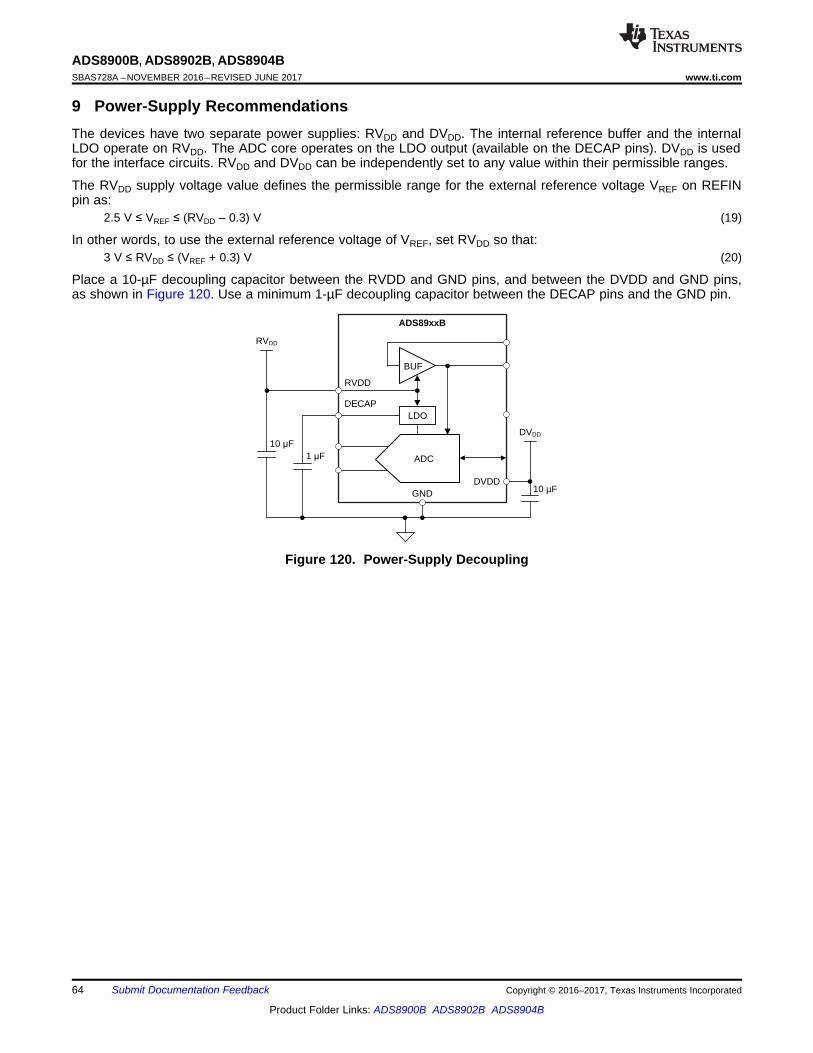
ADC
LDO
BUF
RVDD
DECAP
GND
ADS89xxB
DVDD
RVDD
DVDD
10 �F1 �F
10 µF
64
ADS8900B, ADS8902B, ADS8904BSBAS728A –NOVEMBER 2016–REVISED JUNE 2017 www.ti.com
Product Folder Links: ADS8900B ADS8902B ADS8904B
Submit Documentation Feedback Copyright © 2016–2017, Texas Instruments Incorporated
9 Power-Supply RecommendationsThe devices have two separate power supplies: RVDD and DVDD. The internal reference buffer and the internalLDO operate on RVDD. The ADC core operates on the LDO output (available on the DECAP pins). DVDD is usedfor the interface circuits. RVDD and DVDD can be independently set to any value within their permissible ranges.
The RVDD supply voltage value defines the permissible range for the external reference voltage VREF on REFINpin as:
2.5 V ≤ VREF ≤ (RVDD – 0.3) V (19)
In other words, to use the external reference voltage of VREF, set RVDD so that:3 V ≤ RVDD ≤ (VREF + 0.3) V (20)
Place a 10-µF decoupling capacitor between the RVDD and GND pins, and between the DVDD and GND pins,as shown in Figure 120. Use a minimum 1-µF decoupling capacitor between the DECAP pins and the GND pin.
Figure 120. Power-Supply Decoupling
65
ADS8900B, ADS8902B, ADS8904Bwww.ti.com SBAS728A –NOVEMBER 2016–REVISED JUNE 2017
Product Folder Links: ADS8900B ADS8902B ADS8904B
Submit Documentation FeedbackCopyright © 2016–2017, Texas Instruments Incorporated
10 Layout
10.1 Layout GuidelinesThis section provides some layout guidelines for achieving optimum performance with the ADS890xB devicefamily.
10.1.1 Signal PathAs illustrated in Figure 121, the analog input signals are routed in opposite directions to the digital connections.The reference decoupling components are kept away from the switching digital signals. This arrangementprevents noise generated by digital switching activity from coupling to sensitive analog signals.
10.1.2 Grounding and PCB Stack-UpLow inductance grounding is critical for achieving optimum performance. Grounding inductance is kept below 1nH with 15-mil grounding vias and a printed circuit board (PCB) layout design that has at least four layers. Placeall critical components of the signal chain on the top layer with a solid analog ground from subsequent innerlayers to minimize via length to ground.
For lowest inductance grounding, connect the GND pins of the ADS890xB (pin 11 and pin 15) directly to thedevice thermal pad and place at least four 8-mil grounding vias on the device thermal pad.
10.1.3 Decoupling of Power SuppliesPlace the decoupling capacitors on RVDD, the LDO output, and DVDD within 20 mil from the respective pins, anduse a 15-mil via to ground from each capacitor. Avoid placing vias between any supply pin and the respectivedecoupling capacitor.
10.1.4 Reference DecouplingDynamic currents are also present at the REFBUFOUT and REFM pins during the conversion phase, andexcellent decoupling is required to achieve optimum performance. Place a 22-μF, X7R-grade, ceramic capacitorwith at least 10-V rating and an ESR of 1-Ω between the REFBUFOUT and the REFM pins, as illustrated inFigure 121. Select 0603- or 0805-size capacitors to keep equivalent series inductance (ESL) low. Connect theREFM pins to the decoupling capacitor before a ground via.
10.1.5 Differential Input DecouplingDynamic currents are also present at the differential analog inputs of the ADS890xB. Use C0G- or NPO-typecapacitors to decouple these inputs because with these type of capacitors, capacitance stays almost constantover the full input voltage range. Lower-quality capacitors (such as X5R and X7R) have large capacitancechanges over the full input-voltage range that may cause degradation in the performance of the device.

GND
GNDGND
GND
-
AINM
GND
DifferentialAnalog Input
+
AINP
RV
DD
GND
GND
GND
7
Ext
erna
l R
efer
ence
GND
SDO-3
Digital Inputsand Outputs
DV
DD
SDO-2
SDO-1
SDO-0
RVS
SDI
SCLK
CONVST
CS
RST
GND
1
7
13
19
REFIN
REFM
CREFBUF
RESR
REFBUFOUT
External Reference
Input
Reference Decoupling
Analog Input
Power Supply
66
ADS8900B, ADS8902B, ADS8904BSBAS728A –NOVEMBER 2016–REVISED JUNE 2017 www.ti.com
Product Folder Links: ADS8900B ADS8902B ADS8904B
Submit Documentation Feedback Copyright © 2016–2017, Texas Instruments Incorporated
10.2 Layout Example
Figure 121. Recommended Layout

67
ADS8900B, ADS8902B, ADS8904Bwww.ti.com SBAS728A –NOVEMBER 2016–REVISED JUNE 2017
Product Folder Links: ADS8900B ADS8902B ADS8904B
Submit Documentation FeedbackCopyright © 2016–2017, Texas Instruments Incorporated
11 Device and Documentation Support
11.1 Documentation Support
11.1.1 Related DocumentationFor related documentation see the following:• ADS8900BEVM-PDK User's Guide (SBAU269)• Enabling Faster, Smarter, and More Robust System Solutions for SAR ADCs With TI’s multiSPI™ Digital
Interface (SBAY002)• Ultrasound CW Doppler Summing and 20-bit True Raw Data Conversion Reference Design (TIDA-01351)• 20-Bit, 1-MSPS, 4-Ch Small Form Factor Design for Test and Measurement Applications Reference Design
(TIDUBW7)• 20-Bit, 1-MSPS Isolator Optimized Data Acquisition Reference Design Maximizing SNR and Sample Rate
(TIDA-01037)• A 20-bit,1 MSPS Isolated Data Acquisition (DAQ) Reference Design Optimizing Jitter for Maximum SNR and
Sample Rate (TIDA-01035)• OPAx625 High-Bandwidth, High-Precision, Low THD+N, 16-Bit and 18-Bit Analog-to-Digital Converter (ADC)
Drivers Data Sheet (SBOS688)• REF5050 Low-Noise, Very Low Drift, Precision Voltage Reference Data Sheet (SBOS410)• THS4551 Low Noise, Precision, 150MHz, Fully Differential Amplifier (SBOS778)
11.2 Related LinksThe following table lists quick access links. Categories include technical documents, support and communityresources, tools and software, and quick access to sample or buy.
Table 23. Related Links
PARTS PRODUCT FOLDER SAMPLE & BUY TECHNICALDOCUMENTS
TOOLS &SOFTWARE
SUPPORT &COMMUNITY
ADS8900B Click here Click here Click here Click here Click hereADS8902B Click here Click here Click here Click here Click hereADS8904B Click here Click here Click here Click here Click here
11.3 Receiving Notification of Documentation UpdatesTo receive notification of documentation updates, navigate to the device product folder on ti.com. In the upperright corner, click on Alert me to register and receive a weekly digest of any product information that haschanged. For change details, review the revision history included in any revised document.
11.4 Community ResourcesThe following links connect to TI community resources. Linked contents are provided "AS IS" by the respectivecontributors. They do not constitute TI specifications and do not necessarily reflect TI's views; see TI's Terms ofUse.
TI E2E™ Online Community TI's Engineer-to-Engineer (E2E) Community. Created to foster collaborationamong engineers. At e2e.ti.com, you can ask questions, share knowledge, explore ideas and helpsolve problems with fellow engineers.
Design Support TI's Design Support Quickly find helpful E2E forums along with design support tools andcontact information for technical support.

68
ADS8900B, ADS8902B, ADS8904BSBAS728A –NOVEMBER 2016–REVISED JUNE 2017 www.ti.com
Product Folder Links: ADS8900B ADS8902B ADS8904B
Submit Documentation Feedback Copyright © 2016–2017, Texas Instruments Incorporated
11.5 TrademarksTINA-TI, E2E are trademarks of Texas Instruments.
11.6 Electrostatic Discharge CautionThis integrated circuit can be damaged by ESD. Texas Instruments recommends that all integrated circuits be handled withappropriate precautions. Failure to observe proper handling and installation procedures can cause damage.
ESD damage can range from subtle performance degradation to complete device failure. Precision integrated circuits may be moresusceptible to damage because very small parametric changes could cause the device not to meet its published specifications.
11.7 GlossarySLYZ022 — TI Glossary.
This glossary lists and explains terms, acronyms, and definitions.
12 Mechanical, Packaging, and Orderable InformationThe following pages include mechanical, packaging, and orderable information. This information is the mostcurrent data available for the designated devices. This data is subject to change without notice and revision ofthis document. For browser-based versions of this data sheet, refer to the left-hand navigation.

PACKAGE OPTION ADDENDUM
www.ti.com 2-May-2017
Addendum-Page 1
PACKAGING INFORMATION
Orderable Device Status(1)
Package Type PackageDrawing
Pins PackageQty
Eco Plan(2)
Lead/Ball Finish(6)
MSL Peak Temp(3)
Op Temp (°C) Device Marking(4/5)
Samples
ADS8900BRGER ACTIVE VQFN RGE 24 3000 Green (RoHS& no Sb/Br)
CU NIPDAU Level-2-260C-1 YEAR -40 to 125 8900B
ADS8900BRGET ACTIVE VQFN RGE 24 250 Green (RoHS& no Sb/Br)
CU NIPDAU Level-2-260C-1 YEAR -40 to 125 8900B
ADS8902BRGER ACTIVE VQFN RGE 24 3000 Green (RoHS& no Sb/Br)
CU NIPDAU Level-2-260C-1 YEAR -40 to 125 8902B
ADS8902BRGET ACTIVE VQFN RGE 24 250 Green (RoHS& no Sb/Br)
CU NIPDAU Level-2-260C-1 YEAR -40 to 125 8902B
ADS8904BRGER ACTIVE VQFN RGE 24 3000 Green (RoHS& no Sb/Br)
CU NIPDAU Level-2-260C-1 YEAR -40 to 125 8904B
ADS8904BRGET ACTIVE VQFN RGE 24 250 Green (RoHS& no Sb/Br)
CU NIPDAU Level-2-260C-1 YEAR -40 to 125 8904B
(1) The marketing status values are defined as follows:ACTIVE: Product device recommended for new designs.LIFEBUY: TI has announced that the device will be discontinued, and a lifetime-buy period is in effect.NRND: Not recommended for new designs. Device is in production to support existing customers, but TI does not recommend using this part in a new design.PREVIEW: Device has been announced but is not in production. Samples may or may not be available.OBSOLETE: TI has discontinued the production of the device.
(2) RoHS: TI defines "RoHS" to mean semiconductor products that are compliant with the current EU RoHS requirements for all 10 RoHS substances, including the requirement that RoHS substancedo not exceed 0.1% by weight in homogeneous materials. Where designed to be soldered at high temperatures, "RoHS" products are suitable for use in specified lead-free processes. TI mayreference these types of products as "Pb-Free".RoHS Exempt: TI defines "RoHS Exempt" to mean products that contain lead but are compliant with EU RoHS pursuant to a specific EU RoHS exemption.Green: TI defines "Green" to mean the content of Chlorine (Cl) and Bromine (Br) based flame retardants meet JS709B low halogen requirements of <=1000ppm threshold. Antimony trioxide basedflame retardants must also meet the <=1000ppm threshold requirement.
(3) MSL, Peak Temp. - The Moisture Sensitivity Level rating according to the JEDEC industry standard classifications, and peak solder temperature.
(4) There may be additional marking, which relates to the logo, the lot trace code information, or the environmental category on the device.
(5) Multiple Device Markings will be inside parentheses. Only one Device Marking contained in parentheses and separated by a "~" will appear on a device. If a line is indented then it is a continuationof the previous line and the two combined represent the entire Device Marking for that device.

PACKAGE OPTION ADDENDUM
www.ti.com 2-May-2017
Addendum-Page 2
(6) Lead/Ball Finish - Orderable Devices may have multiple material finish options. Finish options are separated by a vertical ruled line. Lead/Ball Finish values may wrap to two lines if the finishvalue exceeds the maximum column width.
Important Information and Disclaimer:The information provided on this page represents TI's knowledge and belief as of the date that it is provided. TI bases its knowledge and belief on informationprovided by third parties, and makes no representation or warranty as to the accuracy of such information. Efforts are underway to better integrate information from third parties. TI has taken andcontinues to take reasonable steps to provide representative and accurate information but may not have conducted destructive testing or chemical analysis on incoming materials and chemicals.TI and TI suppliers consider certain information to be proprietary, and thus CAS numbers and other limited information may not be available for release.
In no event shall TI's liability arising out of such information exceed the total purchase price of the TI part(s) at issue in this document sold by TI to Customer on an annual basis.

TAPE AND REEL INFORMATION
*All dimensions are nominal
Device PackageType
PackageDrawing
Pins SPQ ReelDiameter
(mm)
ReelWidth
W1 (mm)
A0(mm)
B0(mm)
K0(mm)
P1(mm)
W(mm)
Pin1Quadrant
ADS8900BRGER VQFN RGE 24 3000 330.0 12.4 4.25 4.25 1.15 8.0 12.0 Q2
ADS8900BRGET VQFN RGE 24 250 180.0 12.4 4.25 4.25 1.15 8.0 12.0 Q2
ADS8902BRGER VQFN RGE 24 3000 330.0 12.4 4.25 4.25 1.15 8.0 12.0 Q2
ADS8902BRGET VQFN RGE 24 250 180.0 12.4 4.25 4.25 1.15 8.0 12.0 Q2
ADS8904BRGER VQFN RGE 24 3000 330.0 12.4 4.25 4.25 1.15 8.0 12.0 Q2
ADS8904BRGET VQFN RGE 24 250 180.0 12.4 4.25 4.25 1.15 8.0 12.0 Q2
PACKAGE MATERIALS INFORMATION
www.ti.com 2-May-2017
Pack Materials-Page 1

*All dimensions are nominal
Device Package Type Package Drawing Pins SPQ Length (mm) Width (mm) Height (mm)
ADS8900BRGER VQFN RGE 24 3000 367.0 367.0 35.0
ADS8900BRGET VQFN RGE 24 250 210.0 185.0 35.0
ADS8902BRGER VQFN RGE 24 3000 367.0 367.0 35.0
ADS8902BRGET VQFN RGE 24 250 210.0 185.0 35.0
ADS8904BRGER VQFN RGE 24 3000 367.0 367.0 35.0
ADS8904BRGET VQFN RGE 24 250 210.0 185.0 35.0
PACKAGE MATERIALS INFORMATION
www.ti.com 2-May-2017
Pack Materials-Page 2

GENERIC PACKAGE VIEW
Images above are just a representation of the package family, actual package may vary.Refer to the product data sheet for package details.
RGE 24 VQFN - 1 mm max heightPLASTIC QUAD FLATPACK - NO LEAD
4204104/H

NOTES:
1. All linear dimensions are in millimeters. Any dimensions in parenthesis are for reference only. Dimensioning and tolerancing
per ASME Y14.5M.
2. This drawing is subject to change without notice.
3. The package thermal pad must be soldered to the printed circuit board for thermal and mechanical performance.
PACKAGE OUTLINE
www.ti.com
4219016 / A 08/2017
VQFN - 1 mm max height
PLASTIC QUAD FLATPACK- NO LEAD
RGE0024H
A
0.08 C
0.1 C A B
0.05 C
B
SYMM
SYMM
4.1
3.9
4.1
3.9
PIN 1 INDEX AREA
1 MAX
0.05
0.00
SEATING PLANE
C
2X 2.5
2.7±0.1
2X
2.5
20X 0.5
1
6
7
12
13
18
19
24
24X
0.30
0.18
24X
0.48
0.28
(0.2) TYP
PIN 1 ID
(OPTIONAL)
25

NOTES: (continued)
4. This package is designed to be soldered to a thermal pad on the board. For more information, see Texas Instruments
literature number SLUA271 (www.ti.com/lit/slua271).5. Solder mask tolerances between and around signal pads can vary based on board fabrication site.
EXAMPLE BOARD LAYOUT
4219016 / A 08/2017
www.ti.com
VQFN - 1 mm max height
RGE0024H
PLASTIC QUAD FLATPACK- NO LEAD
SYMM
SYMM
LAND PATTERN EXAMPLE
SCALE: 20X
2X
(1.1)
2X(1.1)
(3.825)
(3.825)
( 2.7)
1
6
7 12
13
18
1924
25
24X (0.58)
24X (0.24)
20X (0.5)
(R0.05)
(Ø0.2) VIA
TYP
SOLDER MASK DETAILS
NON SOLDER MASK
DEFINED
(PREFERRED)
SOLDER MASK
DEFINED
0.07 MAX
ALL AROUND
0.07 MIN
ALL AROUND
METAL
SOLDER MASK
OPENING
SOLDER MASK
OPENING
METAL UNDER
SOLDER MASK

NOTES: (continued)
6. Laser cutting apertures with trapezoidal walls and rounded corners may offer better paste release. IPC-7525 may have alternate
design recommendations..
EXAMPLE STENCIL DESIGN
4219016 / A 08/2017
www.ti.com
VQFN - 1 mm max height
RGE0024H
PLASTIC QUAD FLATPACK- NO LEAD
SYMM
SYMM
SOLDER PASTE EXAMPLE
BASED ON 0.125 mm THICK STENCIL
EXPOSED PAD
78% PRINTED COVERAGE BY AREA
SCALE: 20X
(3.825)
(3.825)
(0.694)
TYP
(0.694)
TYP
4X ( 1.188)
1
6
712
13
18
1924
24X (0.24)
24X (0.58)
20X (0.5)
(R0.05) TYP
METAL
TYP
25

IMPORTANT NOTICE
Texas Instruments Incorporated (TI) reserves the right to make corrections, enhancements, improvements and other changes to itssemiconductor products and services per JESD46, latest issue, and to discontinue any product or service per JESD48, latest issue. Buyersshould obtain the latest relevant information before placing orders and should verify that such information is current and complete.TI’s published terms of sale for semiconductor products (http://www.ti.com/sc/docs/stdterms.htm) apply to the sale of packaged integratedcircuit products that TI has qualified and released to market. Additional terms may apply to the use or sale of other types of TI products andservices.Reproduction of significant portions of TI information in TI data sheets is permissible only if reproduction is without alteration and isaccompanied by all associated warranties, conditions, limitations, and notices. TI is not responsible or liable for such reproduceddocumentation. Information of third parties may be subject to additional restrictions. Resale of TI products or services with statementsdifferent from or beyond the parameters stated by TI for that product or service voids all express and any implied warranties for theassociated TI product or service and is an unfair and deceptive business practice. TI is not responsible or liable for any such statements.Buyers and others who are developing systems that incorporate TI products (collectively, “Designers”) understand and agree that Designersremain responsible for using their independent analysis, evaluation and judgment in designing their applications and that Designers havefull and exclusive responsibility to assure the safety of Designers' applications and compliance of their applications (and of all TI productsused in or for Designers’ applications) with all applicable regulations, laws and other applicable requirements. Designer represents that, withrespect to their applications, Designer has all the necessary expertise to create and implement safeguards that (1) anticipate dangerousconsequences of failures, (2) monitor failures and their consequences, and (3) lessen the likelihood of failures that might cause harm andtake appropriate actions. Designer agrees that prior to using or distributing any applications that include TI products, Designer willthoroughly test such applications and the functionality of such TI products as used in such applications.TI’s provision of technical, application or other design advice, quality characterization, reliability data or other services or information,including, but not limited to, reference designs and materials relating to evaluation modules, (collectively, “TI Resources”) are intended toassist designers who are developing applications that incorporate TI products; by downloading, accessing or using TI Resources in anyway, Designer (individually or, if Designer is acting on behalf of a company, Designer’s company) agrees to use any particular TI Resourcesolely for this purpose and subject to the terms of this Notice.TI’s provision of TI Resources does not expand or otherwise alter TI’s applicable published warranties or warranty disclaimers for TIproducts, and no additional obligations or liabilities arise from TI providing such TI Resources. TI reserves the right to make corrections,enhancements, improvements and other changes to its TI Resources. TI has not conducted any testing other than that specificallydescribed in the published documentation for a particular TI Resource.Designer is authorized to use, copy and modify any individual TI Resource only in connection with the development of applications thatinclude the TI product(s) identified in such TI Resource. NO OTHER LICENSE, EXPRESS OR IMPLIED, BY ESTOPPEL OR OTHERWISETO ANY OTHER TI INTELLECTUAL PROPERTY RIGHT, AND NO LICENSE TO ANY TECHNOLOGY OR INTELLECTUAL PROPERTYRIGHT OF TI OR ANY THIRD PARTY IS GRANTED HEREIN, including but not limited to any patent right, copyright, mask work right, orother intellectual property right relating to any combination, machine, or process in which TI products or services are used. Informationregarding or referencing third-party products or services does not constitute a license to use such products or services, or a warranty orendorsement thereof. Use of TI Resources may require a license from a third party under the patents or other intellectual property of thethird party, or a license from TI under the patents or other intellectual property of TI.TI RESOURCES ARE PROVIDED “AS IS” AND WITH ALL FAULTS. TI DISCLAIMS ALL OTHER WARRANTIES ORREPRESENTATIONS, EXPRESS OR IMPLIED, REGARDING RESOURCES OR USE THEREOF, INCLUDING BUT NOT LIMITED TOACCURACY OR COMPLETENESS, TITLE, ANY EPIDEMIC FAILURE WARRANTY AND ANY IMPLIED WARRANTIES OFMERCHANTABILITY, FITNESS FOR A PARTICULAR PURPOSE, AND NON-INFRINGEMENT OF ANY THIRD PARTY INTELLECTUALPROPERTY RIGHTS. TI SHALL NOT BE LIABLE FOR AND SHALL NOT DEFEND OR INDEMNIFY DESIGNER AGAINST ANY CLAIM,INCLUDING BUT NOT LIMITED TO ANY INFRINGEMENT CLAIM THAT RELATES TO OR IS BASED ON ANY COMBINATION OFPRODUCTS EVEN IF DESCRIBED IN TI RESOURCES OR OTHERWISE. IN NO EVENT SHALL TI BE LIABLE FOR ANY ACTUAL,DIRECT, SPECIAL, COLLATERAL, INDIRECT, PUNITIVE, INCIDENTAL, CONSEQUENTIAL OR EXEMPLARY DAMAGES INCONNECTION WITH OR ARISING OUT OF TI RESOURCES OR USE THEREOF, AND REGARDLESS OF WHETHER TI HAS BEENADVISED OF THE POSSIBILITY OF SUCH DAMAGES.Unless TI has explicitly designated an individual product as meeting the requirements of a particular industry standard (e.g., ISO/TS 16949and ISO 26262), TI is not responsible for any failure to meet such industry standard requirements.Where TI specifically promotes products as facilitating functional safety or as compliant with industry functional safety standards, suchproducts are intended to help enable customers to design and create their own applications that meet applicable functional safety standardsand requirements. Using products in an application does not by itself establish any safety features in the application. Designers mustensure compliance with safety-related requirements and standards applicable to their applications. Designer may not use any TI products inlife-critical medical equipment unless authorized officers of the parties have executed a special contract specifically governing such use.Life-critical medical equipment is medical equipment where failure of such equipment would cause serious bodily injury or death (e.g., lifesupport, pacemakers, defibrillators, heart pumps, neurostimulators, and implantables). Such equipment includes, without limitation, allmedical devices identified by the U.S. Food and Drug Administration as Class III devices and equivalent classifications outside the U.S.TI may expressly designate certain products as completing a particular qualification (e.g., Q100, Military Grade, or Enhanced Product).Designers agree that it has the necessary expertise to select the product with the appropriate qualification designation for their applicationsand that proper product selection is at Designers’ own risk. Designers are solely responsible for compliance with all legal and regulatoryrequirements in connection with such selection.Designer will fully indemnify TI and its representatives against any damages, costs, losses, and/or liabilities arising out of Designer’s non-compliance with the terms and provisions of this Notice.
Mailing Address: Texas Instruments, Post Office Box 655303, Dallas, Texas 75265Copyright © 2018, Texas Instruments Incorporated