adsp-21061 data sheet - · pdf file16 x 40-bit barrel shifter multiplier alu dag1 8 x 4 x 32...
TRANSCRIPT

REV. 0
Information furnished by Analog Devices is believed to be accurate andreliable. However, no responsibility is assumed by Analog Devices for itsuse, nor for any infringements of patents or other rights of third partieswhich may result from its use. No license is granted by implication orotherwise under any patent or patent rights of Analog Devices.
a ADSP-21061 SHARC®*DSP Microcomputer Family
ADSP-21061Pin-Compatible with ADSP-21060 (4 Mbit) and
ADSP-21062 (2 MBit)
5.0 Volt Operation
Low Power (Idle 16) Mode
Flexible Data Formats and 40-Bit Extended Precision
32-Bit Single-Precision and 40-Bit Extended-Precision
IEEE Floating-Point Data Formats
32-Bit Fixed-Point Data Format, Integer and Fractional,
with 80-Bit Accumulators
Parallel Computations
Single-Cycle Multiply and ALU Operations in Parallel with
Dual Memory Read/Writes and Instruction Fetch
Multiply with Add and Subtract for Accelerated FFT
Butterfly Computation
1024-Point Complex FFT Benchmark: 0.46 ms (18,221 Cycles)
1 Megabit Configurable On-Chip SRAM
Dual-Ported for Independent Access by Core Processor
and DMA
Configurable as 32K Words Data Memory (32-Bit), 16K
Words Program Memory (48-Bit) or Combinations of
Both Up to 1 Mbit
One Technology Way, P.O. Box 9106, Norwood, MA 02062-9106, U.S.A.
Tel: 617/329-4700 World Wide Web Site: http://www.analog.com
Fax: 617/326-8703 © Analog Devices, Inc., 1997
SUMMARY
High-Performance Signal Computer for Speech, Sound,
Graphics and Imaging Applications
Super Harvard ARchitecture Computer (SHARC®)—
Four Independent Buses for Dual Data, Instructions,
and I/O
32-Bit IEEE Floating-Point Computation Units—
Multiplier, ALU and Shifter
1 Megabit On-Chip SRAM Memory and Integrated I/O
Peripherals—A Complete System-On-A-Chip
Integrated Multiprocessing Features
KEY FEATURES
40 MIPS, 25 ns Instruction Rate, Single-Cycle Instruction
Execution
120 MFLOPS Peak, 80 MFLOPS Sustained Performance
Dual Data Address Generators with Modulo and Bit-
Reverse Addressing
Efficient Program Sequencing with Zero-Overhead
Looping: Single-Cycle Loop Setup
IEEE JTAG Standard 1149.1 Test Access Port and
On-Chip Emulation
240-Lead PQFP Package
*SHARC is a registered trademark of Analog Devices, Inc.
SERIAL PORTS(2) 6
4
6
IOPREGISTERS
(MEMORY MAPPED)
CONTROL,STATUS, &
DATA BUFFERS
I/O PROCESSOR
TIMER INSTRUCTIONCACHE
32 x 48-BIT
ADDR DATA DATA
DATA
ADDR
ADDR DATA ADDR
TWO INDEPENDENTDUAL-PORTED BLOCKS
PROCESSOR PORT I/O PORT
BL
OC
K 0
BL
OC
K 1 JTAG
TEST &EMULATION
7
HOST PORT
ADDR BUSMUX
IOA17
IOD48
MULTIPROCESSORINTERFACE
DUAL-PORTED SRAM
EXTERNALPORT
DATA BUSMUX
48
3224PM ADDRESS BUS
DM ADDRESS BUS
PM DATA BUS
DM DATA BUS
BUSCONNECT
(PX)
DATAREGISTER
FILE
16 x 40-BIT BARRELSHIFTER
ALUMULTIPLIER
DAG18 x 4 x 32
32
48
40/32
CORE PROCESSOR
DMACONTROLLER
PROGRAMSEQUENCER
DAG28 x 4 x 24
Figure 1. ADSP-21061 Block Diagram

–2–
ADSP-21061
REV. 0
Off-Chip Memory Interfacing
4-Gigawords Addressable (32-Bit Address)
Programmable Wait State Generation, Page-Mode DRAM
Support
DMA Controller
6 DMA Channels
Background DMA Transfers at 40 MHz, in Parallel with
Full-Speed Processor Execution
Performs Transfers Between ADSP-21061 Internal Memory
and External Memory, External Peripherals, Host
Processor, or Serial Ports
Host Processor Interface
Efficient Interface to 16- and 32-Bit Microprocessors
Host can Directly Read/Write ADSP-21061 Internal Memory
Multiprocessing
Glueless Connection for Scalable DSP Multiprocessing
Architecture
Distributed On-Chip Bus Arbitration for Parallel Bus
Connect of Up To 6 ADSP-21061s Plus Host
240 Mbytes/s Transfer Rate Over Parallel Bus
Serial Ports
Two 40 Mbit/s Synchronous Serial Ports
Independent Transmit and Receive Functions
3- to 32-Bit Data Word Width
m-Law/A-Law Hardware Companding
TDM Multichannel Mode
Multichannel Signaling Protocol
Enhanced Multiprocessing Features
FiguresFigure 1. ADSP-21061 Block Diagram . . . . . . . . . . . . . . . . . 1Figure 2. ADSP-21061 System . . . . . . . . . . . . . . . . . . . . . . . 4Figure 3. Multiprocessing System . . . . . . . . . . . . . . . . . . . . . 6Figure 4. ADSP-21062/ADSP-21062L Memory Map . . . . . 7Figure 5. Target Board Connector For ADSP-2106x
EZ-ICE® Emulator (Jumpers in Place) . . . . . . . . . . . . . . . 12Figure 6. JTAG Scan Path Connections for Multiple
ADSP-2106x Systems . . . . . . . . . . . . . . . . . . . . . . . . . . . 12Figure 7. JTAG Clocktree for Multiple ADSP-2106x
Systems . . . . . . . . . . . . . . . . . . . . . . . . . . . . . . . . . . . . . . 13Figure 8. Clock Input . . . . . . . . . . . . . . . . . . . . . . . . . . . . . 16Figure 9. Reset . . . . . . . . . . . . . . . . . . . . . . . . . . . . . . . . . . 16Figure 10. Interrupts . . . . . . . . . . . . . . . . . . . . . . . . . . . . . . 16Figure 11. Timer . . . . . . . . . . . . . . . . . . . . . . . . . . . . . . . . 17Figure 12. Flags . . . . . . . . . . . . . . . . . . . . . . . . . . . . . . . . . 17Figure 13. Memory Read—Bus Master . . . . . . . . . . . . . . . . 18Figure 14. Memory Write—Bus Master . . . . . . . . . . . . . . . 19Figure 15. Synchronous Read/Write—Bus Master . . . . . . . 21Figure 16. Synchronous Read/Write—Bus Slave . . . . . . . . . 23Figure 17. Multiprocessor Bus Request & Host Bus
Request . . . . . . . . . . . . . . . . . . . . . . . . . . . . . . . . . . . . . . 25Figure 18a. Synchronous REDY Timing . . . . . . . . . . . . . . 26Figure 18b. Asynchronous Read/Write—Host to
ADSP-2106x . . . . . . . . . . . . . . . . . . . . . . . . . . . . . . . . . . 27Figure 19. Three-State Timing . . . . . . . . . . . . . . . . . . . . . . 29Figure 20. DMA Handshake Timing . . . . . . . . . . . . . . . . . 31Figure 21. External Late Frame Sync . . . . . . . . . . . . . . . . . 33Figure 22. Serial Ports . . . . . . . . . . . . . . . . . . . . . . . . . . . . 34Figure 23. IEEE 11499.1 JTAG Test Access Port . . . . . . . 35Figure 24. Typical Drive Currents . . . . . . . . . . . . . . . . . . . 36Figure 25. Output Enable/Disable . . . . . . . . . . . . . . . . . . . 37Figure 26. Equivalent Device Loading for AC Measurements
(Includes All Fixtures) . . . . . . . . . . . . . . . . . . . . . . . . . . . 37Figure 27. Voltage Reference Levels for AC Measurements
(Except Output Enable/Disable) . . . . . . . . . . . . . . . . . . . 37Figure 28. Typical Output Rise Time (10%–90% VDD) vs.
Load Capacitance . . . . . . . . . . . . . . . . . . . . . . . . . . . . . . 37Figure 29. Typical Output Rise Time (0.8 V –2.0 V) vs. Load
Capacitance . . . . . . . . . . . . . . . . . . . . . . . . . . . . . . . . . . . 37Figure 30. Typical Output Delay or Hold vs. Load Capacitance
(at Maximum Case Temperature) . . . . . . . . . . . . . . . . . . 37
TABLE OF CONTENTSGENERAL DESCRIPTION . . . . . . . . . . . . . . . . . . . . . . . . . 3ADSP-21000 FAMILY CORE ARCHITECTURE . . . . . . . 4ADSP-21061 FEATURES . . . . . . . . . . . . . . . . . . . . . . . . . . 4ADSP-21061 MEMORY MAP . . . . . . . . . . . . . . . . . . . . . . . 7INTERNAL MEMORY SPACE . . . . . . . . . . . . . . . . . . . . . . 7MULTIPROCESSOR MEMORY SPACE . . . . . . . . . . . . . . 8EXTERNAL MEMORY SPACE . . . . . . . . . . . . . . . . . . . . . 8DEVELOPMENT TOOLS . . . . . . . . . . . . . . . . . . . . . . . . . . 8PIN DESCRIPTIONS . . . . . . . . . . . . . . . . . . . . . . . . . . . . . 9TARGET BOARD CONNECTOR FOR EZ-ICE®*
PROBE . . . . . . . . . . . . . . . . . . . . . . . . . . . . . . . . . . . . . . 12RECOMMENDED OPERATING CONDITIONS . . . . . . 14ELECTRICAL CHARACTERISTICS . . . . . . . . . . . . . . . . 14TIMING SPECIFICATIONS . . . . . . . . . . . . . . . . . . . . . . . 15
Memory Read—Bus Master . . . . . . . . . . . . . . . . . . . . . . . 18Memory Write—Bus Master . . . . . . . . . . . . . . . . . . . . . . 19Synchronous Read/Write—Bus Master . . . . . . . . . . . . . . 20Synchronous Read/Write—Bus Slave . . . . . . . . . . . . . . . . 22Multiprocessor Bus Request and Host Bus Request . . . . . 24Asynchronous Read/Write—Host to ADSP-2106x . . . . . . 26Three-State Timing—Bus Master, Bus Slave,
HBR, SBTS . . . . . . . . . . . . . . . . . . . . . . . . . . . . . . . . . 28DMA Handshake . . . . . . . . . . . . . . . . . . . . . . . . . . . . . . . 30Serial Ports . . . . . . . . . . . . . . . . . . . . . . . . . . . . . . . . . . . . 32JTAG Test Access Port and Emulation . . . . . . . . . . . . . . . 35
OUTPUT DRIVE CURRENTS . . . . . . . . . . . . . . . . . . . . . 36POWER DISSIPATION . . . . . . . . . . . . . . . . . . . . . . . . . . . 36TEST CONDITIONS . . . . . . . . . . . . . . . . . . . . . . . . . . . . 36ENVIRONMENTAL CONDITIONS . . . . . . . . . . . . . . . . 38240-LEAD METRIC PQFP PIN CONFIGURATIONS . . 39PACKAGE DIMENSIONS . . . . . . . . . . . . . . . . . . . . . . . . . 40ORDERING GUIDE . . . . . . . . . . . . . . . . . . . . . . . . . . . . . 40
*EZ-ICE is a registered trademark of Analog Devices Inc.
ADSP-21061
–3–REV. 0
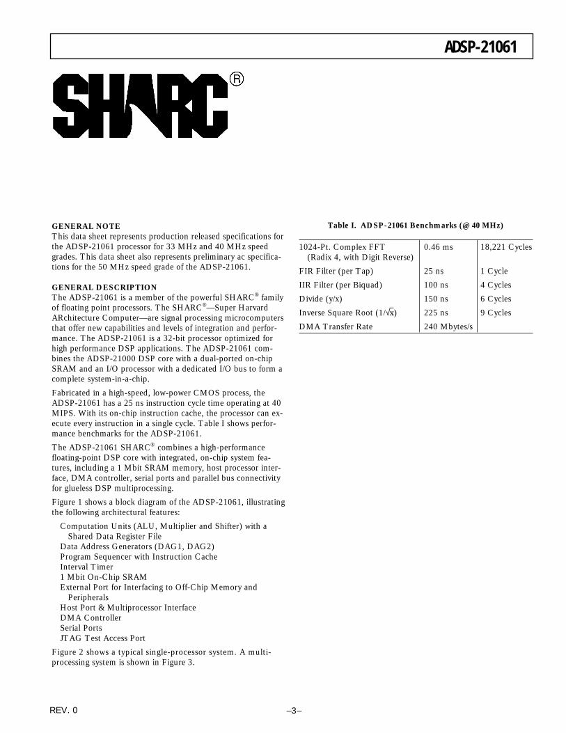
Table I. ADSP-21061 Benchmarks (@ 40 MHz)
1024-Pt. Complex FFT 0.46 ms 18,221 Cycles(Radix 4, with Digit Reverse)
FIR Filter (per Tap) 25 ns 1 Cycle
IIR Filter (per Biquad) 100 ns 4 Cycles
Divide (y/x) 150 ns 6 Cycles
Inverse Square Root (1/√x) 225 ns 9 Cycles
DMA Transfer Rate 240 Mbytes/s
GENERAL NOTEThis data sheet represents production released specifications forthe ADSP-21061 processor for 33 MHz and 40 MHz speedgrades. This data sheet also represents preliminary ac specifica-tions for the 50 MHz speed grade of the ADSP-21061.
GENERAL DESCRIPTIONThe ADSP-21061 is a member of the powerful SHARC® familyof floating point processors. The SHARC®—Super HarvardARchitecture Computer—are signal processing microcomputersthat offer new capabilities and levels of integration and perfor-mance. The ADSP-21061 is a 32-bit processor optimized forhigh performance DSP applications. The ADSP-21061 com-bines the ADSP-21000 DSP core with a dual-ported on-chipSRAM and an I/O processor with a dedicated I/O bus to form acomplete system-in-a-chip.
Fabricated in a high-speed, low-power CMOS process, theADSP-21061 has a 25 ns instruction cycle time operating at 40MIPS. With its on-chip instruction cache, the processor can ex-ecute every instruction in a single cycle. Table I shows perfor-mance benchmarks for the ADSP-21061.
The ADSP-21061 SHARC® combines a high-performancefloating-point DSP core with integrated, on-chip system fea-tures, including a 1 Mbit SRAM memory, host processor inter-face, DMA controller, serial ports and parallel bus connectivityfor glueless DSP multiprocessing.
Figure 1 shows a block diagram of the ADSP-21061, illustratingthe following architectural features:
Computation Units (ALU, Multiplier and Shifter) with aShared Data Register File
Data Address Generators (DAG1, DAG2)Program Sequencer with Instruction CacheInterval Timer1 Mbit On-Chip SRAMExternal Port for Interfacing to Off-Chip Memory and
PeripheralsHost Port & Multiprocessor InterfaceDMA ControllerSerial PortsJTAG Test Access Port
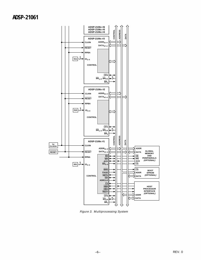
Figure 2 shows a typical single-processor system. A multi-processing system is shown in Figure 3.

–4–
ADSP-21061
REV. 0
ADSP-21000 FAMILY CORE ARCHITECTUREThe ADSP-21061 includes the following architectural featuresof the ADSP-21000 family core. The ADSP-21061 is code andfunction compatible with the ADSP-21060/ADSP-21062.
Independent, Parallel Computation UnitsThe arithmetic/logic unit (ALU), multiplier and shifter all per-form single-cycle instructions. The three units are arranged inparallel, maximizing computational throughput. Single multi-function instructions execute parallel ALU and multiplier opera-tions. These computation units support IEEE 32-bit single-precision floating-point, extended precision 40-bit floating-pointand 32-bit fixed-point data formats.
3
4
RESET JTAG
7
ADSP-21061
BMS
ADDR31–0
DATA47–0
CO
NT
RO
L
AD
DR
ES
S
DA
TA
SERIALDEVICE
(OPTIONAL)
SERIALDEVICE
(OPTIONAL)
CS
ADDR
DATA
BOOTEPROM
(OPTIONAL)
ADDR
ACKCS
MEMORYAND
PERIPHERALS(OPTIONAL)
OEWE
DATA
DMA DEVICE(OPTIONAL)
DATA
ADDR
DATA
HOSTPROCESSORINTERFACE(OPTIONAL)
1x CLOCK
CS
HBR
HBG
REDY
RDWR
PAGE
ADRCLK
ACKMS3–0
SBTSSW
BR1–6
CPA
DMAR1–2DMAG1–2
CLKINEBOOTLBOOT
IRQ2–0
FLAG3–0
TIMEXP
TCLK0RCLK0TFS0RSF0DT0DR0
TCLK1RCLK1TFS1RSF1DT1DR1
RPBAID2–0
TO GND
Figure 2. ADSP-21061 System
Data Register FileA general purpose data register file is used for transferring databetween the computation units and the data buses, and for stor-ing intermediate results. This 10-port, 32-register (16 primary,16 secondary) register file, combined with the ADSP-21000Harvard architecture, allows unconstrained data flow betweencomputation units and internal memory.
Single-Cycle Fetch of Instruction and Two OperandsThe ADSP-21061 features an enhanced Harvard architecture inwhich the data memory (DM) bus transfers data and the pro-gram memory (PM) bus transfers both instructions and data(see Figure 1). With its separate program and data memorybuses and on-chip instruction cache, the processor can simulta-neously fetch two operands and an instruction (from the cache),all in a single cycle.
Instruction CacheThe ADSP-21061 includes an on-chip instruction cache thatenables three-bus operation for fetching an instruction and twodata values. The cache is selective—only the instructions whosefetches conflict with PM bus data accesses are cached. Thisallows full-speed execution of core, looped operations such asdigital filter multiply-accumulates and FFT butterfly processing.
Data Address Generators with Hardware Circular BuffersThe ADSP-21061’s two data address generators (DAGs) imple-ment circular data buffers in hardware. Circular buffers allowefficient programming of delay lines and other data structuresrequired in digital signal processing, and are commonly used indigital filters and Fourier transforms. The ADSP-21061’s twoDAGs contain sufficient registers to allow the creation of up to32 circular buffers (16 primary register sets, 16 secondary). TheDAGs automatically handle address pointer wraparound, reduc-ing overhead, increasing performance and simplifying imple-mentation. Circular buffers can start and end at any memorylocation.
Flexible Instruction SetThe 48-bit instruction word accommodates a variety of paralleloperations, for concise programming. For example, the ADSP-21061 can conditionally execute a multiply, an add, a subtractand a branch, all in a single instruction.
ADSP-21061 FEATURESAugmenting the ADSP-21000 family core, the ADSP-21061adds the following architectural features:
Dual-Ported On-Chip MemoryThe ADSP-21061 contains 1 megabit of on-chip SRAM, orga-nized as two banks of 0.5 Mbits each. Each bank has eight 16-bit columns with 4K 16-bit words per column. Each memoryblock is dual-ported for single-cycle, independent accesses bythe core processor and I/O processor or DMA controller. Thedual-ported memory and separate on-chip buses allow two datatransfers from the core and one from I/O, all in a single cycle.
On the ADSP-21061, the memory can be configured as a maxi-mum of 32K words of 32-bit data, 64K words for 16-bit data,16K words of 48-bit instructions (and 40-bit data) or combina-tions of different word sizes up to 1 megabit. All the memorycan be accessed as 16-bit, 32-bit or 48-bit.
A 16-bit floating-point storage format is supported that effec-tively doubles the amount of data that may be stored on chip.Conversion between the 32-bit floating-point and 16-bit floating-point formats is done in a single instruction.
While each memory block can store combinations of code anddata, accesses are most efficient when one block stores data, us-ing the DM bus for transfers, and the other block stores instruc-tions and data, using the PM bus for transfers. Using the DMand PM buses in this way, with one dedicated to each memoryblock, assures single-cycle execution with two data transfers. Inthis case, the instruction must be available in the cache. Single-cycle execution is also maintained when one of the data oper-ands is transferred to or from off-chip, via the ADSP-21061’sexternal port.

ADSP-21061
–5–REV. 0
Off-Chip Memory and Peripherals InterfaceThe ADSP-21061’s external port provides the processor’s inter-face to off-chip memory and peripherals. The 4-gigaword off-chip address space is included in the ADSP-21061’s unifiedaddress space. The separate on-chip buses—for programmemory, data memory and I/O—are multiplexed at the externalport to create an external system bus with a single 32-bit addressbus and a single 48-bit (or 32-bit) data bus. The on-chipSuper Harvard Architecture provides three-bus performance,while the off-chip unified address space gives flexibility to thedesigner.
Addressing of external memory devices is facilitated by on-chipdecoding of high order address lines to generate memory bankselect signals. Separate control lines are also generated for sim-plified addressing of page-mode DRAM. The ADSP-21061provides programmable memory wait states and external memoryacknowledge controls to allow interfacing to DRAM and peripher-als with variable access, hold and disable time requirements.
Host Processor InterfaceThe ADSP-21061’s host interface allows easy connection tostandard microprocessor buses, both 16-bit and 32-bit, withlittle additional hardware required. Asynchronous transfers atspeeds up to the full clock rate of the processor are supported.The host interface is accessed through the ADSP-21061’s exter-nal port and is memory-mapped into the unified address space.Two channels of DMA are available for the host interface; codeand data transfers are accomplished with low software overhead.
The host processor requests the ADSP-21061’s external buswith the host bus request (HBR), host bus grant (HBG) andready (REDY) signals. The host can directly read and write theinternal memory of the ADSP-21061, and can access the DMAchannel setup and mailbox registers. Vector interrupt support isprovided for efficient execution of host commands.
DMA ControllerThe ADSP-21061’s on-chip DMA controller allows zero-over-head, non-intrusive data transfers without processor interven-tion. The DMA controller operates independently and invisiblyto the processor core, allowing DMA operations to occur whilethe core is simultaneously executing its program instructions.
DMA transfers can occur between the ADSP-21061’s internalmemory and either external memory, external peripherals, or ahost processor. DMA transfers can also occur between theADSP-21061’s internal memory and its serial ports. DMAtransfers between external memory and external peripheraldevices are another option. External bus packing to 16-, 32-or 48-bit words is performed during DMA transfers.
Six channels of DMA are available on the ADSP-21061—fourvia the serial ports, and two via the processor’s external port (foreither host processor, other ADSP-21061s, memory or I/Otransfers). Programs can be downloaded to the ADSP-21061using DMA transfers. Asynchronous off-chip peripherals cancontrol two DMA channels using DMA Request/Grant lines(DMAR1–2, DMAG1–2). Other DMA features include interruptgeneration upon completion of DMA transfers and DMA chain-ing for automatic linked DMA transfers.
Serial PortsThe ADSP-21061 features two synchronous serial ports thatprovide an inexpensive interface to a wide variety of digital andmixed-signal peripheral devices. The serial ports can operate atthe full clock rate of the processor, providing each with a maxi-mum data rate of 40 Mbit/s. Independent transmit and receivefunctions provide greater flexibility for serial communications.Serial port data can be automatically transferred to and fromon-chip memory via DMA. Each of the serial ports offers TDMmultichannel mode.
The serial ports can operate with little-endian or big-endiantransmission formats, with word lengths selectable from threebits to 32 bits. They offer selectable synchronization and trans-mit modes as well as optional µ-law or A-law companding.Serial port clocks and frame syncs can be internally or externallygenerated. The serial ports also include keyword and keymaskfeatures to enhance interprocessor communication.
MultiprocessingThe ADSP-21061 offers powerful features tailored to multipro-cessing DSP systems. The unified address space allows directinterprocessor accesses of each ADSP-21061’s internal memory.Distributed bus arbitration logic is included on-chip for simple,glueless connection of systems containing up to six ADSP-21061sand a host processor. Master processor changeover incurs onlyone cycle of overhead. Bus arbitration is selectable as eitherfixed or rotating priority. Bus lock allows indivisible read-modify-write sequences for semaphores. A vector interrupt is providedfor interprocessor commands. Maximum throughput for inter-processor data transfer is 240 Mbytes/sec over the external port.Broadcast writes allow simultaneous transmission of data toall ADSP-21061s and can be used to implement reflectivesemaphores.
Program BootingThe internal memory of the ADSP-21061 can be booted at sys-tem power-up from either an 8-bit EPROM or a host processor.Selection of the boot source is controlled by the BMS (BootMemory Select), EBOOT (EPROM Boot), and LBOOT (HostBoot) pins. 32-bit and 16-bit host processors can be used forbooting. See the BMS pin in the Pin Descriptions section of thisdata sheet.
–6–
ADSP-21061
REV. 0
ADDR31–0
DATA47–0
BMS
CONTROL
ADSP-2106x #1
5
CONTROL
ADSP-2106x #2
ADDR31–0
DATA47–0
CPA
BR1–2, BR4-6
BR3
CONTROL
ADSP-2106x #3
5
3011 ID2–0
RESET
RPBA
CLKIN
ADSP-2106x #6ADSP-2106x #5ADSP-2106x #4
CO
NT
RO
L
AD
DR
ES
S
DA
TA
1xCLOCK
ADDR
DATA
HOSTPROCESSORINTERFACE(OPTIONAL)
ACKCS
GLOBALMEMORY
ANDPERIPHERALS
(OPTIONAL)
OEWE
ADDR
DATA
CS
ADDR
DATA
BOOTEPROM
(OPTIONAL)
RDWR
MS3–0
SBTSSW
ADRCLK
CSHBRHBG
REDY
ACK
ADDR31–0
DATA47–0
5
3010 ID2–0
RPBA
CLKIN
ID2–0
RPBA
CLKIN
3001
CO
NT
RO
L
AD
DR
ES
S
DA
TA
PAGE
CPA
BR1–2, BR3-6
BR2
RESET
RESET
CPA
BR2-6
BR1
RESET
Figure 3. Multiprocessing System

ADSP-21061
–7–REV. 0
IOP REGISTERS
NORMAL WORD ADDRESSING
0x0000 0000
0x0002 0000
0x0004 0000
0x0008 0000
0x0010 0000
0x0018 0000
0x0020 0000
0x0028 0000
0x0030 0000
0x0038 0000
INTERNALMEMORY
SPACE
0x003F FFFF
SHORT WORD ADDRESSING
INTERNAL MEMORY SPACEOF ADSP-2106x
WITH ID=010
INTERNAL MEMORY SPACEOF ADSP-2106x
WITH ID=001
INTERNAL MEMORY SPACEOF ADSP-2106x
WITH ID=011
INTERNAL MEMORY SPACEOF ADSP-2106x
WITH ID=100
INTERNAL MEMORY SPACEOF ADSP-2106x
WITH ID=101
INTERNAL MEMORY SPACEOF ADSP-2106x
WITH ID=110
BROADCAST WRITETO ALL
ADSP-2106xs
MULTIPROCESSORMEMORY SPACE
NORMAL WORD ADDRESSING: 32-BIT DATA WORDS 48-BIT INSTRUCTION WORDSSHORT WORD ADDRESSING: 16-BIT DATA WORDS
BANK 0
0x0040 0000
0xFFFF FFFF
BANK 1
BANK 2
DRAM(OPTIONAL)
BANK 3
NONBANKED
MS3
BANK SIZE ISSELECTED BYMSIZE BIT FIELD OFSYSCONREGISTER.
EXTERNALMEMORY
SPACE
MS2
MS1
MS0
Figure 4. ADSP-21062/ADSP-21062L Memory Map

–8–
ADSP-21061
REV. 0
Porting Code from ADSP-21060 or ADSP-21062 to theADSP-21061The ADSP-21061 is pin compatible with the ADSP-21060/62.The ADSP-21061 pins that correspond to the Link Port pins ofthe ADSP-21060/62 are no-connects.
The ADSP-21061 is object code compatible with the ADSP-21060/62 except for the following functional changes:
The ADSP-21061 memory is organized into two blocks witheight columns that are 4K deep per block. The ADSP-21060/ADSP-21062 memory has 16 columns per block.Link port functions are not available.Handshake external port DMA pins DMAR2 and DMAG2are assigned to external port DMA Channel 6 instead ofChannel 8.2-D DMA capability of the SPORT is not available.DMA channels 8 and 9 are not available.The modify registers in SPORT DMA are not programmable.
On the ADSP-21061, Block 0 starts at the beginning of internalmemory, normal word address 0x0002 0000. Block 1 starts atthe end of Block 0, with contiguous addresses. The remainingaddresses in internal memory are divided into blocks that aliasinto Block 1. This allows any code or data stored in Block 1 onthe ADSP-21062 to retain the same addresses on the ADSP-21061—these addresses will alias into the actual Block 1 of eachprocessor.
If you develop your application using the ADSP-21062, but willmigrate to the ADSP-21061, use only the first eight columns ofeach memory bank. Limit your application to 8K of instructionsor up to 16K of data in each bank of the ADSP-21062, or anycombinations of instructions or data that does not exceed thememory bank.
DEVELOPMENT TOOLSThe ADSP-21061 is supported with a complete set of softwareand hardware development tools, including an EZ-ICE® In-Cir-cuit Emulator, EZ-Kit Lite, and development software. TheSHARC® EZ-Kit Lite* is a complete low cost package for DSPevaluation and prototyping. The EZ-Kit Lite contains an evalu-ation board with an ADSP-21061 (5 V) processor and providesa serial connection to your PC. The EZ-Kit Lite also includesan optimizing compiler, assembler, instruction level simulator,run-time libraries, diagnostic utilities and a complete set of ex-ample programs.
The same EZ-ICE hardware can be used for the ADSP-21060/ADSP-21062, to fully emulate the ADSP-21061, with the excep-tion of displaying and modifying the two new SPORTS regis-ters. The emulator will not display these two registers, butyour code can use them.
CBUG and SHARCPAC are trademarks of Analog Devices, Inc.
Analog Devices ADSP-21000 Family Development Software in-cludes an easy to use Assembler based on an algebraic syntax,Assembly Library/Librarian, Linker, instruction-level Simulator,an ANSI C optimizing Compiler, the CBug™ C Source—LevelDebugger and a C Runtime Library including DSP and math-ematical functions. The Optimizing Compiler includes Numeri-cal C extensions based on the work of the ANSI Numerical CExtensions Group. Numerical C provides extensions to the Clanguage for array selections, vector math operations, complexdata types, circular pointers and variably dimensioned arrays.The ADSP-21000 Family Development Software is available forboth the PC and Sun platforms.
The ADSP-21061 EZ-ICE® Emulator uses the IEEE 1149.1JTAG test access port of the ADSP-21061 processor to monitorand control the target board processor during emulation. TheEZ-ICE® provides full-speed emulation, allowing inspection andmodification of memory, registers, and processor stacks. Nonin-trusive in-circuit emulation is assured by the use of the processor’sJTAG interface—the emulator does not affect target systemloading or timing.
Further details and ordering information are available in theADSP-21000 Family Hardware and Software Development Toolsdata sheet (ADDS-210xx-TOOLS). This data sheet can be re-quested from any Analog Devices sales office or distributor.
In addition to the software and hardware development toolsavailable from Analog Devices, third parties provide a widerange of tools supporting the SHARC® processor family. Hard-ware tools include SHARC® PC plug-in cards multiprocessorSHARC® VME boards, and daughter and modules with mul-tiple SHARC®s’ and additional memory. These modules arebased on the SHARCPAC™ module specification. Third Partysoftware tools include an Ada compiler, DSP libraries, operatingsystems and block diagram design tools.
ADDITIONAL INFORMATIONThis data sheet provides a general overview of the ADSP-21061architecture and functionality. For detailed information on theADSP-21000 Family core architecture and instruction set, referto the ADSP-2106x SHARC™ User’s Manual, Second Edition.
*ADDS-2106x-EZ-LITE

ADSP-21061
–9–REV. 0
PIN DESCRIPTIONSADSP-21061 pin definitions are listed below. Inputs identifiedas synchronous (S) must meet timing requirements with respectto CLKIN (or with respect to TCK for TMS, TDI). Inputsidentified as asynchronous (A) can be asserted asynchronouslyto CLKIN (or to TCK for TRST).
Unused inputs should be tied or pulled to IVDD or IGND,except for ADDR31-0, DATA47-0, FLAG3-0, SW and inputs thathave internal pull-up or pull-down resistors (CPA, ACK, DTx,
DRx, TCLKx, RCLKx, TMS and TDI)—these pins can be leftfloating. These pins have a logic-level hold circuit that preventsthe input from floating internally.
I = Input S = Synchronous P = Power Supply(O/D) = Open Drain O = Output A = AsynchronousG = Ground (A/D) = Active DriveT = Three-State (when SBTS is asserted, or when theADSP-2106x is a bus slave)
PIN FUNCTION DESCRIPTIONS
Pin Type Function
ADDR31-0 I/O/T External Bus Address. The ADSP-21061 outputs addresses for external memory and peripheralson these pins. In a multiprocessor system the bus master outputs addresses for read/writes of the in-ternal memory or IOP registers of other ADSP-2106xs. The ADSP-21061 inputs addresses when a hostprocessor or multiprocessing bus master is reading or writing its internal memory or IOP registers.
DATA47-0 I/O/T External Bus Data. The ADSP-21061 inputs and outputs data and instructions on these pins.The external data bus transfers 32-bit single-precision floating-point data and 32-bit fixed-pointdata over Bits 47-16. 40-bit extended-precision floating-point data is transferred over Bits 47-8 ofthe bus. 16-bit short word data is transferred over Bits 31-16 of the bus. Pull-up resistors on un-used DATA pins are not necessary.
MS3-0 O/T Memory Select Lines. These lines are asserted (low) as chip selects for the corresponding banksof external memory. Memory bank size must be defined in the ADSP-21061’s system control regis-ter (SYSCON). The MS3-0 lines are decoded memory address lines that change at the same time asthe other address lines. When no external memory access is occurring the MS3-0 lines are inactive;they are active, however, when a conditional memory access instruction is executed, whether or notthe condition is true. MS0 can be used with the PAGE signal to implement a bank of DRAMmemory (Bank 0). In a multiprocessor system the MS3-0 lines are output by the bus master.
RD I/O/T Memory Read Strobe. This pin is asserted (low) when the ADSP-21061 reads from externalmemory devices or from the internal memory of other ADSP-21061s. External devices (includingother ADSP-21061s) must assert RD to read from the ADSP-21061’s internal memory. In a multi-processor system RD is output by the bus master and is input by all other ADSP-21061s.
WR I/O/T Memory Write Strobe. This pin is asserted (low) when the ADSP-21061 writes to externalmemory devices or to the internal memory of other ADSP-21061s. External devices must assertWR to write to the ADSP-21061’s internal memory. In a multiprocessor system WR is output bythe bus master and is input by all other ADSP-21061s.
PAGE O/T DRAM Page Boundary. The ADSP-21061 asserts this pin to signal that an external DRAM pageboundary has been crossed. DRAM page size must be defined in the ADSP-21061’s memory con-trol register (WAIT). DRAM can only be implemented in external memory Bank 0; the PAGE sig-nal can only be activated for Bank 0 accesses. In a multiprocessor system PAGE is output by thebus master.
ADRCLK O/T Address Clock for synchronous external memories. Addresses on ADDR31-0 are valid before therising edge of ADRCLK. In a multiprocessing system ADRCLK is output by the bus master.
SW I/O/T Synchronous Write Select. This signal is used to interface the ADSP-2106x to synchronousmemory devices (including other ADSP-21061s). The ADSP-21061 asserts SW (low) to providean early indication of an impending write cycle, which can be aborted if WR is not later asserted(e.g. in a conditional write instruction). In a multiprocessor system, SW is output by the bus masterand is input by all other ADSP-21061s to determine if the multiprocessor memory access is a reador write. SW is asserted at the same time as the address output. A host processor using synchronouswrites must assert this pin when writing to the ADSP-21061(s).
ACK I/O/S Memory Acknowledge. External devices can deassert ACK (low) to add wait states to an externalmemory access. ACK is used by I/O devices, memory controllers or other peripherals to hold offcompletion of an external memory access. The ADSP-21061 deasserts ACK as an output to addwait states to a synchronous access of its internal memory. In a multiprocessor system, a slaveADSP-21061 deasserts the bus master’s ACK input to add wait state(s) to an access of its internalmemory. The bus master has a keeper latch on its ACK pin that maintains the input at the level itwas last driven to.

–10–
ADSP-21061
REV. 0
Pin Type Function
SBTS I/S Suspend Bus Three-State. External devices can assert SBTS (low) to place the external bus address,data, selects, and strobes in a high impedance state for the following cycle. If the ADSP-21061attempts to access external memory while SBTS is asserted, the processor will halt and the memoryaccess will not be completed until SBTS is deasserted. SBTS should only be used to recover fromPAGE faults or host processor/ADSP-21061 deadlock.
IRQ2-0 I/A Interrupt Request Lines. May be either edge-triggered or level-sensitive.
FLAG3-0 I/O/A Flag Pins. Each is configured via control bits as either an input or an output. As an input, it can betested as a condition. As an output, it can be used to signal external peripherals.
TIMEXP O Timer Expired. Asserted for four cycles when the timer is enabled and TCOUNT decrements tozero.
HBR I/A Host Bus Request. Must be asserted by a host processor to request control of the ADSP-21061’sexternal bus. When HBR is asserted in a multiprocessing system, the ADSP-21061 that is bus masterwill relinquish the bus and assert HBG. To relinquish the bus, the ADSP-21061 places the address,data, select, and strobe lines in a high impedance state. HBR has priority over all ADSP-21061 busrequests (BR6-1) in a multiprocessing system.
HBG I/O Host Bus Grant. Acknowledges an HBR bus request, indicating that the host processor may takecontrol of the external bus. HBG is asserted (held low) by the ADSP-21061 until HBR is released. In amultiprocessing system, HBG is output by the ADSP-21061 bus master and is monitored by all others.
CS I/A Chip Select. Asserted by host processor to select the ADSP-21061.
REDY (O/D) O Host Bus Acknowledge. The ADSP-2106x deasserts REDY (low) to add wait states to an asynchro-nous access of its internal memory or IOP registers by a host. Open drain output (O/D) by default; canbe programmed in ADREDY bit of SYSCON register to be active drive (A/D). REDY will only beoutput if the CS and HBR inputs are asserted.
DMAR1 I/A DMA Request 1 (DMA Channel 7).
DMAR2 I/A DMA Request 2 (DMA Channel 6).
DMAG1 O/T DMA Grant 1 (DMA Channel 7).
DMAG2 O/T DMA Grant 2 (DMA Channel 6).
BR6-1 I/O/S Multiprocessing Bus Requests. Used by multiprocessing ADSP-21061s to arbitrate for bus master-ship. An ADSP-21061 only drives its own BRx line (corresponding to the value of its ID2-0 inputs) andmonitors all others. In a multiprocessor system with less than six ADSP-21061s, the unused BRx pinsshould be tied high; the processor’s own BRx line must not be tied high or low because it is an output.
ID2-0 I Multiprocessing ID. Determines which multiprocessing bus request (BR1–BR6) is used by ADSP-21061. ID = 001 corresponds to BR1, ID = 010 corresponds to BR2, etc. ID = 000 in single-processor sys-tems. These lines are a system configuration selection which should be hardwired or only changed at reset.
RPBA I/S Rotating Priority Bus Arbitration Select. When RPBA is high, rotating priority for multiprocessorbus arbitration is selected. When RPBA is low, fixed priority is selected. This signal is a system con-figuration selection which must be set to the same value on every ADSP-21061. If the value of RPBA ischanged during system operation, it must be changed in the same CLKIN cycle on every ADSP-21061.
CPA (O/D) I/O Core Priority Access. Asserting its CPA pin allows the core processor of an ADSP-21061 bus slaveto interrupt background DMA transfers and gain access to the external bus. CPA is an open drain out-put that is connected to all ADSP-2106xs in the system. The CPA pin has an internal 5 kΩ pull-upresistor. If core access priority is not required in a system, the CPA pin should be left unconnected.
DTx O Data Transmit (Serial Ports 0, 1). Each DT pin has a 50 kΩ internal pull-up resistor.
DRx I Data Receive (Serial Ports 0, 1). Each DR pin has a 50 kΩ internal pull-up resistor.
TCLKx I/O Transmit Clock (Serial Ports 0, 1). Each TCLK pin has a 50 kΩ internal pull-up resistor.
RCLKx I/O Receive Clock (Serial Ports 0, 1). Each RCLK pin has a 50 kΩ internal pull-up resistor.

ADSP-21061
–11–REV. 0
Pin Type Function
TFSx I/O Transmit Frame Sync (Serial Ports 0, 1).
RFSx I/O Receive Frame Sync (Serial Ports 0, 1).
EBOOT I EPROM Boot Select. When EBOOT is high, the ADSP-21061 is configured for booting from an 8-bit EPROM. When EBOOT is low, the LBOOT and BMS inputs determine booting mode. See tablebelow. This signal is a system configuration selection which should be hardwired.
LBOOT I Link Boot—Must be tied to GND.
BMS I/O/T* Boot Memory Select. Output: Used as chip select for boot EPROM devices (when EBOOT = 1,LBOOT = 0). In a multiprocessor system, BMS is output by the bus master. Input: When low, indi-cates that no booting will occur and that ADSP-21061 will begin executing instructions from externalmemory. See table below. This input is a system configuration selection which should be hardwired.
*Three-statable only in EPROM boot mode (when BMS is an output).
EBOOT LBOOT BMS Booting Mode
1 0 Output EPROM (Connect BMS to EPROM chip select.)0 0 1 (Input) Host Processor0 0 0 (Input) No Booting. Processor executes from external memory.
CLKIN I Clock In. External clock input to the ADSP-21061. The instruction cycle rate is equal to CLKIN.CLKIN may not be halted, changed, or operated below the specified frequency.
RESET I/A Processor Reset. Resets the ADSP-21061 to a known state and begins execution at the programmemory location specified by the hardware reset vector address. This input must be asserted (low) atpower-up.
TCK I Test Clock (JTAG). Provides an asynchronous clock for JTAG boundary scan.
TMS I/S Test Mode Select (JTAG). Used to control the test state machine. TMS has a 20 kΩ internal pull-upresistor.
TDI I/S Test Data Input (JTAG). Provides serial data for the boundary scan logic. TDI has a 20 kΩ internalpull-up resistor.
TDO O Test Data Output (JTAG). Serial scan output of the boundary scan path.
TRST I/A Test Reset (JTAG). Resets the test state machine. TRST must be asserted (pulsed low) after power-up or held low for proper operation of the ADSP-21061. TRST has a 20 kΩ internal pull-up resistor.
EMU O Emulation Status. Must be connected to the ADSP-21061 EZ-ICE® target board connector only.
ICSA O Reserved, leave unconnected.
VDD P Power Supply; nominally +5.0 V dc. (30 pins)
GND G Power Supply Return. (30 pins)
NC Do Not Connect. Reserved pins which must be left open and unconnected.
–12–
ADSP-21061
REV. 0
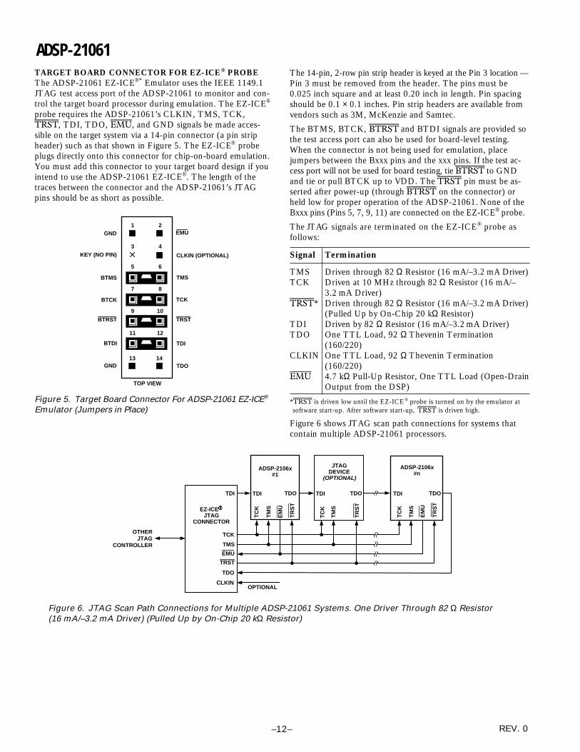
The 14-pin, 2-row pin strip header is keyed at the Pin 3 location —Pin 3 must be removed from the header. The pins must be0.025 inch square and at least 0.20 inch in length. Pin spacingshould be 0.1 × 0.1 inches. Pin strip headers are available fromvendors such as 3M, McKenzie and Samtec.
The BTMS, BTCK, BTRST and BTDI signals are provided sothe test access port can also be used for board-level testing.When the connector is not being used for emulation, placejumpers between the Bxxx pins and the xxx pins. If the test ac-cess port will not be used for board testing, tie BTRST to GNDand tie or pull BTCK up to VDD. The TRST pin must be as-serted after power-up (through BTRST on the connector) orheld low for proper operation of the ADSP-21061. None of theBxxx pins (Pins 5, 7, 9, 11) are connected on the EZ-ICE® probe.
The JTAG signals are terminated on the EZ-ICE® probe asfollows:
Signal Termination
TMS Driven through 82 Ω Resistor (16 mA/–3.2 mA Driver)TCK Driven at 10 MHz through 82 Ω Resistor (16 mA/–
3.2 mA Driver)TRST* Driven through 82 Ω Resistor (16 mA/–3.2 mA Driver)
(Pulled Up by On-Chip 20 kΩ Resistor)TDI Driven by 82 Ω Resistor (16 mA/–3.2 mA Driver)TDO One TTL Load, 92 Ω Thevenin Termination
(160/220)CLKIN One TTL Load, 92 Ω Thevenin Termination
(160/220)EMU 4.7 kΩ Pull-Up Resistor, One TTL Load (Open-Drain
Output from the DSP)
*TRST is driven low until the EZ-ICE® probe is turned on by the emulator atsoftware start-up. After software start-up, TRST is driven high.
Figure 6 shows JTAG scan path connections for systems thatcontain multiple ADSP-21061 processors.
TARGET BOARD CONNECTOR FOR EZ-ICE® PROBEThe ADSP-21061 EZ-ICE®* Emulator uses the IEEE 1149.1JTAG test access port of the ADSP-21061 to monitor and con-trol the target board processor during emulation. The EZ-ICE®
probe requires the ADSP-21061’s CLKIN, TMS, TCK,TRST, TDI, TDO, EMU, and GND signals be made acces-sible on the target system via a 14-pin connector (a pin stripheader) such as that shown in Figure 5. The EZ-ICE® probeplugs directly onto this connector for chip-on-board emulation.You must add this connector to your target board design if youintend to use the ADSP-21061 EZ-ICE®. The length of thetraces between the connector and the ADSP-21061’s JTAGpins should be as short as possible.
TOP VIEW
13 14
11 12
9 10
9
7 8
5 6
3 4
1 2EMU
CLKIN (OPTIONAL)
TMS
TCK
TRST
TDI
TDO
GND
KEY (NO PIN)
BTMS
BTCK
BTRST
BTDI
GND
Figure 5. Target Board Connector For ADSP-21061 EZ-ICE®
Emulator (Jumpers in Place)
ADSP-2106x#1
JTAGDEVICE
(OPTIONAL)
ADSP-2106x#n
TDI
EZ-ICEJTAG
CONNECTOR
OTHERJTAG
CONTROLLER
OPTIONAL
TC
K
TM
S
EMU
TMS
TCK
TDO
CLKIN
TRST
TC
K
TM
S
TC
K
TM
S
TDI TDO TDI TDO TDOTDI
EM
U
TR
ST
EM
U
TR
ST
TR
ST
Figure 6. JTAG Scan Path Connections for Multiple ADSP-21061 Systems. One Driver Through 82 Ω Resistor(16 mA/–3.2 mA Driver) (Pulled Up by On-Chip 20 kΩ Resistor)

ADSP-21061
–13–REV. 0
Connecting CLKIN to Pin 4 of the EZ-ICE® header is optional.The emulator only uses CLKIN when directed to performoperations such as starting, stopping and single-stepping mul-tiple ADSP-21061s in a synchronous manner. If you do not needthese operations to occur synchronously on the multiple proces-sors, simply tie Pin 4 of the EZ-ICE® header to ground.
If synchronous multiprocessor operations are needed andCLKIN is connected, clock skew between the multiple ADSP-21061 processors and the CLKIN pin on the EZ-ICE®* headermust be minimal. If the skew is too large, synchronous operationsmay be off by one cycle between processors. For synchronousmultiprocessor operation TCK, TMS, CLKIN and EMU
should be treated as critical signals in terms of skew, and shouldbe laid out as short as possible on your board. If TCK, TMSand CLKIN are driving a large number of ADSP-21061s (morethan eight) in your system, then treat them as a clock tree usingmultiple drivers to minimize skew. (See Figure 7, JTAG ClockTree, and Clock Distribution in the High Frequency DesignConsiderations section of the ADSP-2106x User’s Manual.)
If synchronous multiprocessor operations are not needed (i.e.,CLKIN is not connected), just use appropriate parallel termina-tion on TCK and TMS. TDI, TDO, EMU and TRST are notcritical signals in terms of skew.
SYSTEMCLKIN
5kΩ*
TDI TDO
5kΩ*
TDI
EMU
TMS
TCK
TDO
TRST
CLKIN
*OPEN DRAIN DRIVER OR EQUIVALENT, i.e.,
TDI TDO TDI TDO
TDI TDO TDI TDO TDI TDO
EMU
Figure 7. JTAG Clocktree for Multiple ADSP-21061 Systems
REV. 0–14–
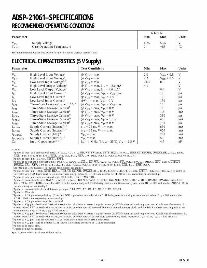
ADSP-21061–SPECIFICATIONSRECOMMENDED OPERATING CONDITIONS
K GradeParameter Min Max Units
VDD Supply Voltage 4.75 5.25 VTCASE Case Operating Temperature 0 +85 °C
See Environmental Conditions section for information on thermal specifications.
ELECTRICAL CHARACTERISTICS (5 V Supply)Parameter Test Conditions Min Max Units
VIH1 High Level Input Voltage1 @ VDD = max 2.0 VDD + 0.5 VVIH2 High Level Input Voltage2 @ VDD = max 2.2 VDD + 0.5 VVIL Low Level Input Voltage1, 2 @ VDD = min –0.5 0.8 VVOH High Level Output Voltage3 @ VDD = min, IOH = – 2.0 mA4 4.1 VVOL Low Level Output Voltage3 @ VDD = min, IOL = 4.0 mA4 0.4 VIIH High Level Input Current5 @ VDD = max, VIN = VDD max 10 µAIIL Low Level Input Current5 @ VDD = max, VIN = 0 V 10 µAIILP Low Level Input Current6 @VDD = max, VIN = 0 V 150 µAIOZH Three-State Leakage Current7, 8, 9, 10 @ VDD = max, VIN = VDD max 10 µAIOZL Three-State Leakage Current7 @ VDD = max, VIN = 0 V 10 µAIOZLC Three-State Leakage Current9 @ VDD = max, VIN = 0 V 1.5 mAIOZLA Three-State Leakage Current11 @ VDD = max, VIN = 0 V 350 µAIOZLAR Three-State Leakage Current10 @ VDD = max, VIN = 1.5 V 4.0 mAIOZLS Three-State Leakage Current8 @ VDD = max, VIN = 0 V 150 µAIDDIN1 Supply Current (Internal)12 tCK = 25 ns, VDD = max, 850 mAIDDIN2 Supply Current (Internal)13 tCK = 25 ns, VDD = max, 650 mAIDDIDLE Supply Current (Idle)14 VDD = max 200 mAIDDIDLE16 Supply Current (Idle16)15 VDD = max 50 mACIN Input Capacitance16, 17 fIN = 1 MHz, TCASE = 25°C, VIN = 2.5 V 4.7 pF
NOTES1Applies to input and bidirectional pins: DATA 47-0, ADDR31-0, RD, WR, SW, ACK, SBTS, IRQ2-0, FLAG3-0, HBG, CS, DMAR1, DMAR2, BR6-1, ID2-0, RPBA,CPA, TFS0, TFS1, RFS0, RFS1, BMS, TMS, TDI, TCK, HBR, DR0, DR1, TCLK0, TCLK1, RCLK0, RCLK1.
2Applies to input pins: CLKIN, RESET, TRST.3Applies to output and bidirectional pins: DATA47-0, ADDR31-0, MS3-0, RD, WR, PAGE, ADRCLK, SW, ACK, FLAG3-0, TIMEXP, HBG, REDY, DMAG1,DMAG2, BR6-1, CPA, DT0, DT1, TCLK0, TCLK1, RCLK0, RCLK1, TFS0, TFS1, RFS0, RFS1, BMS, TDO, EMU, ICSA.
4See “Output Drive Currents” for typical drive current capabilities.5Applies to input pins: ACK, SBTS, IRQ2-0, HBR, CS, DMAR1, DMAR2, ID2-0, RPBA, EBOOT, LBOOT, CLKIN, RESET, TCK. (Note that ACK is pulled upinternally with 2 kΩ during reset in a multiprocessor system, when ID2-0 = 001 and another ADSP-2106x is not requesting bus mastership.)
6Applies to input pins with internal pull-ups: DR0, DR1, TRST, TMS, TDI.7Applies to three-statable pins: DATA47-0, ADDR31-0, MS3-0, RD, WR, PAGE, ADRCLK, SW, ACK, FLAG3-0, REDY, HBG, DMAG1, DMAG2, BMS, TDO,BR6-1, TFSX, RFSX, EMU. (Note that ACK is pulled up internally with 2 kΩ during reset in a multiprocessor system, when ID2-0 = 001 and another ADSP-2106x isnot requesting bus mastership.)
8Applies to three-statable pins with internal pull-ups: DT0, DT1, TCLK0, TCLK1, RCLK0, RCLK1.9Applies to CPA pin.
10Applies to ACK pin when pulled up. (Note that ACK is pulled up internally with a 2 k Ω during reset in a multiprocessor system, when ID2-0 = 001 and anotherADSP-21061 is not requesting bus mastership).
11Applies to ACK pin when keeper latch enabled.12Applies to VDD pins. See Power Dissipation section for calculation of external supply current (at EVDD pins) and total supply current. Conditions of operation: Ex-
ecuting radix-2 FFT butterfly with instruction in cache, one data operand accessed from each internal memory block, and one DMA transfer occurring from/to in-ternal memory at tCK = 30 ns, IDDIN = 750 mA max.
13Applies to VDD pins. See Power Dissipation section for calculation of external supply current (at EVDD pins) and total supply current. Conditions of operations: Ex-ecuting radix-2 FFT butterfly with instruction in cache, one data operand fetched from each memory block, memory at t CK = 30 ns, IDDIN2 = 540 mA max.
14Applies to VDD pins. Idle denotes ADSP-21061 state during execution of IDLE instruction.15Applies to VDD pins. Idle 16 denotes ADSP-21061 state during execution of IDLE16 instruction.16Applies to all signal pins.17Guaranteed but not tested.
Specifications subject to change without notice.

ADSP-21061
–15–REV. 0
ABSOLUTE MAXIMUM RATINGS*Supply Voltage . . . . . . . . . . . . . . . . . . . . . . . –0.3 V to +7.0 VInput Voltage . . . . . . . . . . . . . . . . . . . . –0.5 V to VDD + 0.5 VOutput Voltage Swing . . . . . . . . . . . . . –0.5 V to VDD + 0.5 VLoad Capacitance . . . . . . . . . . . . . . . . . . . . . . . . . . . . 200 pFJunction Temperature Under Bias . . . . . . . . . . . . . . . . 130°CStorage Temperature Range . . . . . . . . . . . . –65°C to +150°CLead Temperature (5 seconds) . . . . . . . . . . . . . . . . . +280°C*Stresses greater than those listed above may cause permanent damage to thedevice. These are stress ratings only; functional operation of the device at these orany other conditions greater than those indicated in the operational sections of thisspecification is not implied. Exposure to absolute maximum rating conditions forextended periods may affect device reliability.
ESD SENSITIVITYThe ADSP-2106x processors are ESD (electrostatic discharge) sensitive devices. Electro-static charges readily accumulate on the human body and equipment and can dischargewithout detection. Permanent damage may occur to devices subjected to high energyelectrostatic discharges.
The ADSP-21061 processors include proprietary ESD protection circuitry to dissipatehigh energy discharges. Per method 3015 of MIL-STD-883, the ADSP-2106x processorshave been classified as a Class 2 device.
Proper ESD precautions are recommended to avoid performance degradation or loss offunctionality. Unused devices must be stored in conductive foam or shunts, and the foamshould be discharged to the destination socket before devices are removed.
TIMING SPECIFICATIONSGENERAL NOTESThis data sheet represents production released specifications forthe ADSP-21061 processor for 33 MHz and 40 MHz speedgrades. This data sheet also represents preliminary ac specifica-tions for the 50 MHz speed grade of the ADSP-21061.
The specifications shown are based on a CLKIN frequency of40 MHz (tCK = 25 ns). The DT derating allows specifications atother CLKIN frequencies (within the min–max range of the tCK
specification; see Clock Input below). DT is the difference be-tween the actual CLKIN period and a CLKIN period of 25 ns:
DT = tCK – 25 ns
Use the exact timing information given. Do not attempt toderive parameters from the addition or subtraction of others.While addition or subtraction would yield meaningful results foran individual device, the values given in this data sheet reflectstatistical variations and worst cases. Consequently, you cannotmeaningfully add parameters to derive longer times.
See Figure 28 under Test Conditions for voltage referencelevels.
Switching Characteristics specify how the processor changes itssignals. You have no control over this timing—circuitry externalto the processor must be designed for compatibility with thesesignal characteristics. Switching characteristics tell you what theprocessor will do in a given circumstance. You can also use switch-ing characteristics to ensure that any timing requirement of a de-vice connected to the processor (such as memory) is satisfied.
Timing Requirements apply to signals that are controlled by cir-cuitry external to the processor, such as the data input for aread operation. Timing requirements guarantee that the proces-sor operates correctly with other devices.
(O/D) = Open Drain
(A/D) = Active Drive
WARNING!
ESD SENSITIVE DEVICE

–16–
ADSP-21061
REV. 0
50 MHz* 40 MHz 33.3 MHzParameter Min Max Min Max Min Max Units
Clock Input
Timing Requirements:tCK CLKIN Period 20 100 25 100 30 100 nstCKL CLKIN Width Low 7 7 7 nstCKH CLKIN Width High 5 5 5 nstCKRF CLKIN Rise/Fall (0.4 V–2.0 V) 3 3 ns
*50 MHz specifications are preliminary.
CLKIN
tCKH
tCK
tCKL
Figure 8. Clock Input
Parameter Min Max Units
Reset
Timing Requirements:tWRST RESET Pulse Width Low1 4tCK nstSRST RESET Setup Before CLKIN High2 14 + DT/2 tCK ns
NOTES1Applies after the power-up sequence is complete. At power-up, the processor’s internal phase-locked loop requires no more than 2000 CLKIN cycles while RESET islow, assuming stable VDD and CLKIN (not including start-up time of external clock oscillator).
2Only required if multiple ADSP-2106xs must come out of reset synchronous to CLKIN with program counters (PC) equal (i.e., for a SIMD system). Not requiredfor multiple ADSP-2106xs communicating over the shared bus (through the external port), because the bus arbitration logic automatically synchronizes itself after reset.
CLKIN
RESET
tWRST
tSRST
Figure 9. Reset
Parameter Min Max Units
InterruptsTiming Requirements:tSIR IRQ2-0 Setup Before CLKIN High1 18 + 3DT/4 nstHIR IRQ2-0 Hold Before CLKIN High1 12 + 3DT/4 nstIPW IRQ2-0 Pulse Width2 2 + tCK ns
NOTES1Only required for IRQx recognition in the following cycle.2Applies only if tSIR and tHIR requirements are not met.
CLKIN
IRQ2-0
tIPW
tSIR
tHIR
Figure 10. Interrupts

ADSP-21061
–17–REV. 0
Parameter Min Max Units
TimerSwitching Characteristics:tDTEX CLKIN High to TIMEXP 15 ns
CLKIN
tDTEX tDTEX
TIMEXP
Figure 11. Timer
Parameter Min Max Units
FlagsTiming Requirements:tSFI FLAG3-0IN Setup Before CLKIN High1 8 + 5DT/16 nstHFI FLAG3-0IN Hold After CLKIN High1 0 – 5DT/16 nstDWRFI FLAG3-0IN Delay After RD/WR Low1 5 + 7DT/16 nstHFIWR FLAG3-0IN Hold After RD/WR Deasserted1 0 ns
Switching Characteristics:tDFO FLAG3-0OUT Delay After CLKIN High 16 nstHFO FLAG3-0OUT Hold After CLKIN High 4 nstDFOE CLKIN High to FLAG2-0OUT Enable 3 nstDFOD CLKIN High to FLAG2-0OUT Disable 14 ns
NOTE1Flag inputs meeting these setup and hold times will affect conditional instructions in the following instruction cycle.
CLKIN
FLAG3–0OUT
FLAG OUTPUT
tDFO tHFO
tDFO tDFOD
tDFOE
CLKIN
RD, WR
FLAG INPUT
tSFI
tHFI
tHFIWR tDWRFI
FLAG3–0IN
Figure 12. Flags
–18–
ADSP-21061
REV. 0
Parameter Min Max Units
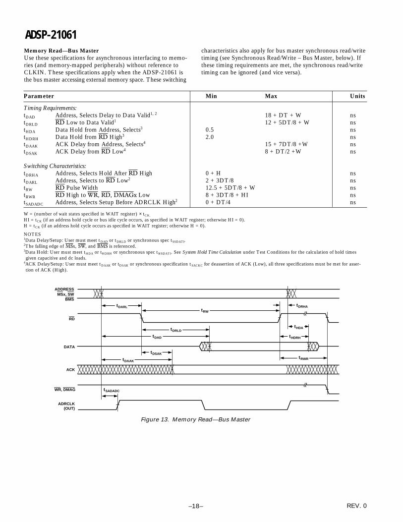
Timing Requirements:tDAD Address, Selects Delay to Data Valid1, 2 18 + DT + W nstDRLD RD Low to Data Valid1 12 + 5DT/8 + W nstHDA Data Hold from Address, Selects3 0.5 nstHDRH Data Hold from RD High3 2.0 nstDAAK ACK Delay from Address, Selects4 15 + 7DT/8 +W nstDSAK ACK Delay from RD Low4 8 + DT/2 +W ns
Switching Characteristics:tDRHA Address, Selects Hold After RD High 0 + H nstDARL Address, Selects to RD Low2 2 + 3DT/8 nstRW RD Pulse Width 12.5 + 5DT/8 + W nstRWR RD High to WR, RD, DMAGx Low 8 + 3DT/8 + HI nstSADADC Address, Selects Setup Before ADRCLK High2 0 + DT/4 ns
W = (number of wait states specified in WAIT register) × tCK.
HI = tCK (if an address hold cycle or bus idle cycle occurs, as specified in WAIT register; otherwise HI = 0).H = tCK (if an address hold cycle occurs as specified in WAIT register; otherwise H = 0).
NOTES1Data Delay/Setup: User must meet tDAD or tDRLD or synchronous spec tSSDATI.2The falling edge of MSx, SW, and BMS is referenced.3Data Hold: User must meet tHDA or tHDRH or synchronous spec tHSDATI. See System Hold Time Calculation under Test Conditions for the calculation of hold timesgiven capacitive and dc loads.
4ACK Delay/Setup: User must meet tDAAK or tDSAK or synchronous specification tSACKC for deassertion of ACK (Low), all three specifications must be met for asser-tion of ACK (High).
WR, DMAG
ACK
DATA
RD
ADDRESSMSx, SW
BMS
tDARL tRW
tDAD
tSADADC
tDAAK
tHDRH
tHDA
tRWR
tDRLD
ADRCLK (OUT)
tDRHA
tDSAK
Figure 13. Memory Read—Bus Master
Memory Read—Bus MasterUse these specifications for asynchronous interfacing to memo-ries (and memory-mapped peripherals) without reference toCLKIN. These specifications apply when the ADSP-21061 isthe bus master accessing external memory space. These switching
characteristics also apply for bus master synchronous read/writetiming (see Synchronous Read/Write – Bus Master, below). Ifthese timing requirements are met, the synchronous read/writetiming can be ignored (and vice versa).

ADSP-21061
–19–REV. 0
Parameter Min Max Units
Timing Requirements:tDAAK ACK Delay from Address, Selects1, 2 15 + 7DT/8 +W nstDSAK ACK Delay from WR Low1 8 + DT/2 +W ns
Switching Characteristics:tDAWH Address, Selects to WR Deasserted2 17 + 15DT/16 +W nstDAWL Address, Selects to WR Low2 3 + 3DT/8 nstWW WR Pulse Width 13 + 9DT/16 +W nstDDWH Data Setup before WR High 7 + DT/2 +W nstDWHA Address Hold after WR Deasserted 1 + DT/16 + H nstDATRWH Data Disable after WR Deasserted3 1 + DT/16 + H 6 + DT/16 + H nstWWR WR High to WR, RD, DMAGx Low 8 + 7DT/16 + H nstDDWR Data Disable before WR or RD Low 5 + 3DT/8 + I nstWDE WR Low to Data Enabled –1 + DT/16 nstSADADC Address, Selects to ADRCLK High2 0 + DT/4 ns
W = (number of wait states specified in WAIT register) × tCK.H = tCK (if an address hold cycle occurs, as specified in WAIT register; otherwise H = 0).I = tCK (if a bus idle cycle occurs, as specified in WAIT register; otherwise I = 0).
NOTES1ACK Delay/Setup: User must meet tDAAK or tDSAK or synchronous specification tSACKC for deassertion of ACK (Low), all three specifications must be met for asser-tion of ACK (High)
2The falling edge of MSx, SW, and BMS is referenced.3See System Hold Time Calculation under Test Conditions for calculation of hold times given capacitive and dc loads.
RD , DMAG
ACK
DATA
WR
ADDRESSMSx , SW
BMS
tDAWL tWW
tSADADC
tDAAK
tWWR tWDE
ADRCLK(OUT)
tDDWR tDATRWH
tDWHA
tDDWH
tDAWH
tDSAK
Figure 14. Memory Write—Bus Master
Memory Write—Bus MasterUse these specifications for asynchronous interfacing to memo-ries (and memory-mapped peripherals) without reference toCLKIN. These specifications apply when the ADSP-21061 isthe bus master accessing external memory space. These switching
characteristics also apply for bus master synchronous read/writetiming (see Synchronous Read/Write–Bus Master). If these tim-ing requirements are met, the synchronous read/write timingcan be ignored (and vice versa).

–20–
ADSP-21061
REV. 0
Synchronous Read/Write—Bus MasterUse these specifications for interfacing to external memory sys-tems that require CLKIN—relative timing or for accessing aslave ADSP-21061 (in multiprocessor memory space). Thesesynchronous switching characteristics are also valid during asyn-chronous memory reads and writes (see Memory Read—BusMaster and Memory Write—Bus Master).
When accessing a slave ADSP-2106x, these switching character-istics must meet the slave’s timing requirements for synchronousread/writes (see Synchronous Read/Write—Bus Slave). Theslave ADSP-21061 must also meet these (bus master) timingrequirements for data and acknowledge setup and hold times.
Parameter Min Max Units
Timing Requirements:tSSDATI Data Setup Before CLKIN 2 + DT/8 nstHSDATI Data Hold After CLKIN 3.5 – DT/8 nstDAAK ACK Delay After Address, MSx, SW, BMS1, 2 14 + 7 DT/8 + W nstSACKC ACK Setup Before CLKIN2 6.5 + DT/4 nstHACKC ACK Hold After CLKIN –1 – DT/4 ns
Switching Characteristics:tDADRO Address, MSx, BMS, SW Delay After CLKIN1 7 – DT/8 nstHADRO Address, MSx, BMS, SW Hold After CLKIN –1 – DT/8 nstDPGC PAGE Delay After CLKIN 9 + DT/8 16 + DT/8 nstDRDO RD High Delay After CLKIN –1.5 – DT/8 4 – DT/8 nstDWRO WR High Delay After CLKIN –2.5 – 3DT/16 4 – 3DT/16 nstDRWL RD/WR Low Delay After CLKIN 8 + DT/4 12 + DT/4 nstSDDATO Data Delay After CLKIN 19 + 5DT/16 nstDATTR Data Disable After CLKIN3 0 – DT/8 7 – DT/8 nstDADCCK ADRCLK Delay After CLKIN 4 + DT/8 10 + DT/8 nstADRCK ADRCLK Period tCK nstADRCKH ADRCLK Width High (tCK/2 – 2) nstADRCKL ADRCLK Width Low (tCK/2 – 2) ns
W = (number of Wait states specified in WAIT register) × tCK.
NOTE1ACK Delay/Setup: User must meet tDAAK or tDSAK or synchronous specification tSACKC for deassertion of ACK (Low), all three specifications must be met for assertionof ACK (High)
2The falling edge of MSx, SW, and BMS is referenced.3See System Hold Time Calculation under Test Conditions for calculation of hold times given capacitive and dc loads.

ADSP-21061
–21–REV. 0
CLKIN
ADRCLK
ADDRESSSW
ACK (IN)
PAGE
RD
DATA(OUT)
WR
tDADCCK
tADRCK
tADRCKL
tHADRO tDAAK
tDPGC
tDRWL
tSACKC
tHACKC
tHSDATI
tSSDATI
tDRDO
tDWRO
tDATTR tSDDATO
tDRWL
DATA (IN)
tDADRO
tADRCKH
WRITE CYCLE
READ CYCLE
Figure 15. Synchronous Read/Write—Bus Master

–22–
ADSP-21061
REV. 0
Synchronous Read/Write—Bus SlaveUse these specifications for ADSP-21061 bus master accesses ofa slave’s IOP registers or internal memory (in multiprocessor
memory space). The bus master must meet these (bus slave)timing requirements.
Parameter Min Max Units
Timing Requirements:tSADRI Address, SW Setup Before CLKIN 14 + DT/2 nstHADRI Address, SW Hold Before CLKIN 5 + DT/2 nstSRWLI RD/WR Low Setup Before CLKIN1 8.5 + 5DT/16 nstHRWLI RD/WR Low Hold After CLKIN –4 – 5DT/16 8 + 7DT/16 nstRWHPI RD/WR Pulse High 3 nstSDATWH Data Setup Before WR High 3 nstHDATWH Data Hold After WR High 1 ns
Switching Characteristics:tSDDATO Data Delay After CLKIN 19 + 5DT/16 nstDATTR Data Disable After CLKIN2 0 – DT/8 7 – DT/8 nstDACKAD ACK Delay After Address, SW3 8 nstACKTR ACK Disable After CLKIN3 –1 – DT/8 6 – DT/8 ns
NOTES1tSRWLI (min) = 8.5 + 5DT/16 when Multiprocessor Memory Space Wait State (MMSWS bit in WAIT register) is disabled; when MMSWS is enabled, t SRWLI (min)= 4 + DT/8.
2See System Hold Time Calculation under Test Conditions for calculation of hold times given capacitive and dc loads.3tDACKAD is true only if the address and SW inputs have setup times (before CLKIN) greater than 10 + DT/8 and less than 19 + 3DT/4. If the address and SW inputs havesetup times greater than 19 + 3DT/4, then ACK is valid 14 + DT/4 (max) after CLKIN. A slave that sees an address with an M field match will respond with ACKregardless of the state of MMSWS or strobes. A slave will three-state ACK every cycle with t ACKTR.

ADSP-21061
–23–REV. 0
CLKIN
ADDRESSSW
ACK
RD
DATA (OUT)
WR
WRITE ACCESS
tSADRI tHADRI
tDACKAD tACKTR
tRWHPI tHRWLI tSRWLI
tSDDATO tDATTR
tSRWLI tHRWLI tRWHPI
tHDATWH tSDATWH
DATA(IN)
READ ACCESS
Figure 16. Synchronous Read/Write—Bus Slave
–24–
ADSP-21061
REV. 0
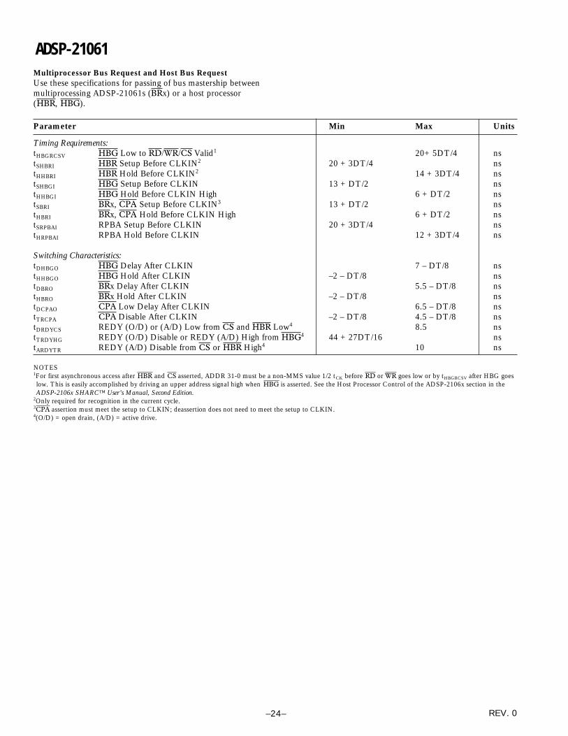
Parameter Min Max Units
Timing Requirements:tHBGRCSV HBG Low to RD/WR/CS Valid1 20+ 5DT/4 nstSHBRI HBR Setup Before CLKIN2 20 + 3DT/4 nstHHBRI HBR Hold Before CLKIN2 14 + 3DT/4 nstSHBGI HBG Setup Before CLKIN 13 + DT/2 nstHHBGI HBG Hold Before CLKIN High 6 + DT/2 nstSBRI BRx, CPA Setup Before CLKIN3 13 + DT/2 nstHBRI BRx, CPA Hold Before CLKIN High 6 + DT/2 nstSRPBAI RPBA Setup Before CLKIN 20 + 3DT/4 nstHRPBAI RPBA Hold Before CLKIN 12 + 3DT/4 ns
Switching Characteristics:tDHBGO HBG Delay After CLKIN 7 – DT/8 nstHHBGO HBG Hold After CLKIN –2 – DT/8 nstDBRO BRx Delay After CLKIN 5.5 – DT/8 nstHBRO BRx Hold After CLKIN –2 – DT/8 nstDCPAO CPA Low Delay After CLKIN 6.5 – DT/8 nstTRCPA CPA Disable After CLKIN –2 – DT/8 4.5 – DT/8 nstDRDYCS REDY (O/D) or (A/D) Low from CS and HBR Low4 8.5 nstTRDYHG REDY (O/D) Disable or REDY (A/D) High from HBG4 44 + 27DT/16 nstARDYTR REDY (A/D) Disable from CS or HBR High4 10 ns
NOTES1For first asynchronous access after HBR and CS asserted, ADDR 31-0 must be a non-MMS value 1/2 tCK before RD or WR goes low or by tHBGRCSV after HBG goeslow. This is easily accomplished by driving an upper address signal high when HBG is asserted. See the Host Processor Control of the ADSP-2106x section in theADSP-2106x SHARC™ User’s Manual, Second Edition.
2Only required for recognition in the current cycle.3CPA assertion must meet the setup to CLKIN; deassertion does not need to meet the setup to CLKIN.4(O/D) = open drain, (A/D) = active drive.
Multiprocessor Bus Request and Host Bus RequestUse these specifications for passing of bus mastership betweenmultiprocessing ADSP-21061s (BRx) or a host processor(HBR, HBG).

ADSP-21061
–25–REV. 0
CLKIN
HBR
HBG(OUT)
BRx(OUT)
HBG (IN)
BRx (IN)
HBR
REDY (O/D)
CS
HBG (OUT)
tDRDYCS
tHBGRCSV
tTRDYHG
REDY (A/D)
tARDYTR
tSRPBAI tHRPBAI
RPBA
tSHBRI tHHBRI
tHHBGO
tDHBGO
tHBRO
tDBRO
tDCPAO tTRCPA
tSHBGI
tSBRI
CPA (OUT) (O/D)
CPA (IN) (O/D)
tHHBGI
tHBRI
O/D = OPEN DRAIN, A/D = ACTIVE DRIVE
Figure 17. Multiprocessor Bus Request and Host Bus Request

–26–
ADSP-21061
REV. 0
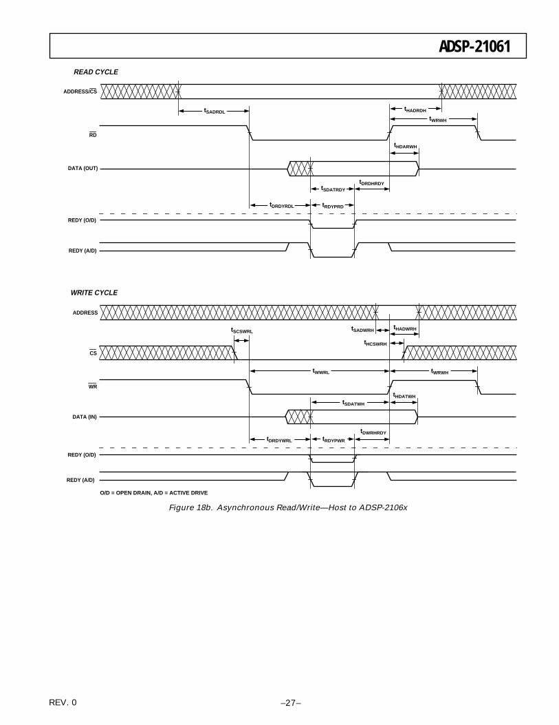
Parameter Min Max Units
Read CycleTiming Requirements:tSADRDL Address Setup/CS Low Before RD Low1 0 nstHADRDH Address Hold/CS Hold Low After RD 0 nstWRWH RD/WR High Width 6 nstDRDHRDY RD High Delay After REDY (O/D) Disable 0 nstDRDHRDY RD High Delay After REDY (A/D) Disable 0 ns
Switching Characteristics:tSDATRDY Data Valid Before REDY Disable from Low 2 nstDRDYRDL REDY (O/D) or (A/D) Low Delay After RD Low 10 nstRDYPRD REDY (O/D) or (A/D) Low Pulse
Width for Read 45 + DT nstHDARWH Data Disable After RD High 2 8 ns
Write CycleTiming Requirements:tSCSWRL CS Low Setup Before WR low 0tHCSWRH CS Low Hold After WR high 0tSADWRH Address Setup Before WR High 5 nstHADWRH Address Hold After WR High 2 nstWWRL WR Low Width 7 nstWRWH RD/WR High Width 6 nstDWRHRDY WR High Delay After REDY
(O/D) or (A/D) Disable 0 nstSDATWH Data Setup Before WR High 3 nstHDATWH Data Hold After WR High 1 ns
Switching Characteristics:tDRDYWRL REDY (O/D) or (A/D) Low Delay
After WR/CS Low 10 nstRDYPWR REDY (O/D) or (A/D) Low Pulse
Width for Write 15 nstSRDYCK REDY (O/D) or (A/D) Disable to CLKIN 1 + 7DT/16 8 + 7DT/16 ns
NOTE1Not required if RD and address are valid tHBGRCSV after HBG goes low. For first access after HBR asserted, ADDR 31-0 must be a non-MMS value 1/2 tCLK beforeRD or WR goes low or by tHBGRCSV after HBG goes low. This is easily accomplished by driving an upper address signal high when HBG is asserted. See the Host Pro-cessor Control of the ADSP-2106x section in the ADSP-2106x SHARC™ User’s Manual.
CLKIN
REDY (O/D)
O/D = OPEN DRAIN, A/D = ACTIVE DRIVE
tSRDYCK
REDY (A/D)
Figure 18a. Synchronous REDY Timing
Asynchronous Read/Write—Host to ADSP-21061Use these specifications for asynchronous host processor accessesof an ADSP-21061, after the host has asserted CS and HBR(low). After HBG is returned by the ADSP-21061, the host can
drive the RD and WR pins to access the ADSP-21061’s internalmemory or IOP registers. HBR and HBG are assumed low forthis timing.
ADSP-21061
–27–REV. 0
tSADRDL
REDY (O/D)
RD
tDRDYRDL
tWRWH
tHADRDH
tHDARWH
tRDYPRD
tDRDHRDY tSDATRDY
READ CYCLE
ADDRESS/CS
DATA (OUT)
REDY (A/D)
O/D = OPEN DRAIN, A/D = ACTIVE DRIVE
tSDATWH
tHDATWH
tWWRL
REDY (O/D)
WR
tDRDYWRL
tWRWH
tHADWRH
tRDYPWR
tDWRHRDY
WRITE CYCLE
tSADWRH
DATA (IN)
ADDRESS
REDY (A/D)
tSCSWRL
CS
tHCSWRH
Figure 18b. Asynchronous Read/Write—Host to ADSP-2106x

–28–
ADSP-21061
REV. 0
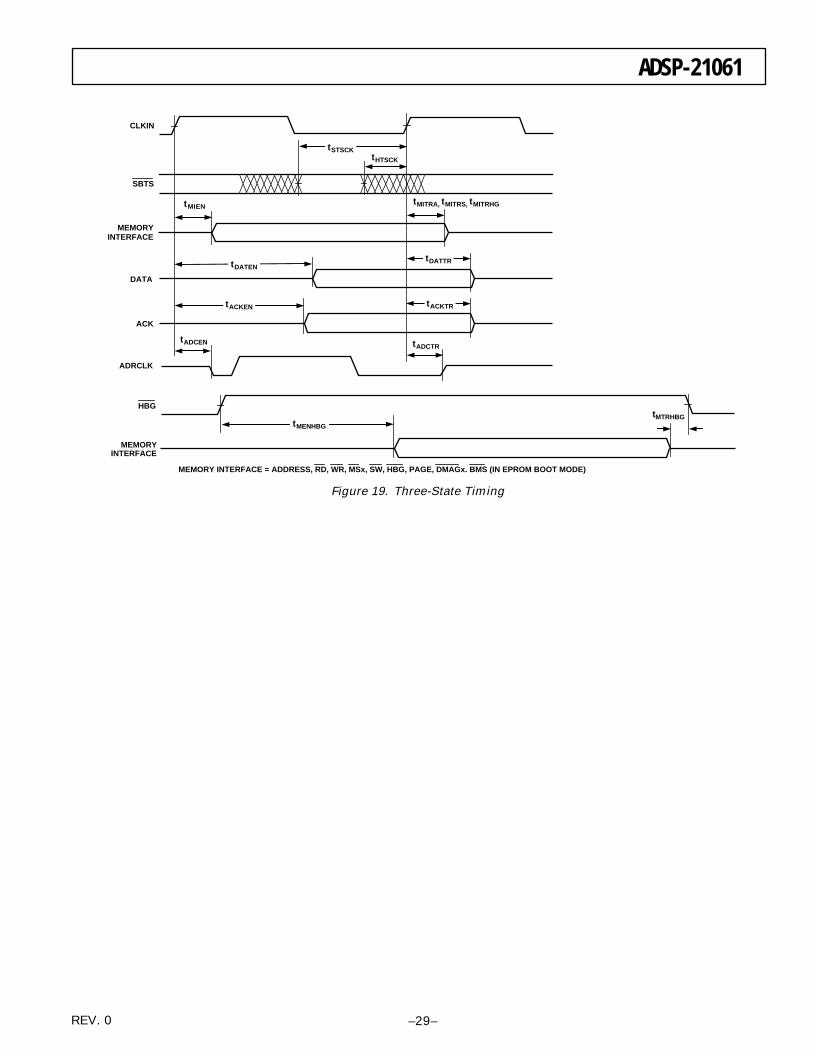
Parameter Min Max Units
Timing Requirements:tSTSCK SBTS Setup Before CLKIN 12 + DT/2 nstHTSCK SBTS Hold Before CLKIN 6 + DT/2 ns
Switching Characteristics:tMIENA Address/Select Enable After CLKIN –1 – DT/8 nstMIENS Strobes Enable After CLKIN1 –1.5 – DT/8 nstMIENHG HBG Enable After CLKIN –1.5 – DT/8 nstMITRA Address/Select Disable After CLKIN 0 – DT/4 nstMITRS Strobes Disable After CLKIN1 1.5 – DT/4 nstMITRHG HBG Disable After CLKIN 2.0 – DT/4 nstDATEN Data Enable After CLKIN2 9 + 5DT/16 nstDATTR Data Disable After CLKIN2 0 – DT/8 7 – DT/8 nstACKEN ACK Enable After CLKIN2 7.5 + DT/4 nstACKTR ACK Disable After CLKIN2 –1 – DT/8 6 – DT/8 nstADCEN ADRCLK Enable After CLKIN –2 – DT/8 nstADCTR ADRCLK Disable After CLKIN 8 – DT/4 nstMTRHBG Memory Interface Disable Before HBG Low3 0 + DT/8 nstMENHBG Memory Interface Enable After HBG High3 19 + DT ns
NOTES1Strobes = RD, WR, MSx, SW, PAGE, DMAG, BMS.2In addition to bus master transition cycles, these specs also apply to bus master and bus slave synchronous read/write.3Memory Interface = Address, RD, WR, MSx, SW, HBG, PAGE, DMAGx, BMS (in EPROM boot mode).
Three-State Timing—Bus Master, Bus Slave, HBR, SBTSThese specifications show how the memory interface is disabled(stops driving) or enabled (resumes driving) relative to CLKINand the SBTS pin. This timing is applicable to bus master tran-sition cycles (BTC) and host transition cycles (HTC) as well asthe SBTS pin.
ADSP-21061
–29–REV. 0
CLKIN
SBTS
ACK
MEMORYINTERFACE
tMENHBG
tMTRHBG
HBG
MEMORY INTERFACE = ADDRESS, RD, WR, MSx, SW, HBG, PAGE, DMAGx. BMS (IN EPROM BOOT MODE)
tMITRA, tMITRS, tMITRHG
tSTSCKtHTSCK
tDATTRtDATEN
tACKTRtACKEN
tADCTRtADCEN
ADRCLK
DATA
tMIEN
MEMORYINTERFACE
Figure 19. Three-State Timing

–30–
ADSP-21061
REV. 0
Parameter Min Max Units
Timing Requirements:tSDRLC DMARx Low Setup Before CLKIN1 5 nstSDRHC DMARx High Setup Before CLKIN1 5 nstWDR DMARx Width Low (Nonsynchronous) 6 nstSDATDGL Data Setup After DMAGx Low2 10 + 5DT/8 nstHDATIDG Data Hold After DMAGx High 2 nstDATDRH Data Valid After DMARx High2 16 + 7DT/8 nstDMARLL DMARx Low Edge to Low Edge 23 + 7DT/8 nstDMARH DMARx Width High 6 ns
Switching Characteristics:tDDGL DMAGx Low Delay After CLKIN 9 + DT/4 15 + DT/4 nstWDGH DMAGx High Width 6 + 3DT/8 nstWDGL DMAGx Low Width 12 + 5DT/8 nstHDGC DMAGx High Delay After CLKIN –2 – DT/8 6 – DT/8 nstDADGH Address Select Valid to DMAGx High 17 + DT nstDDGHA Address Select Hold to DMAGx High –0.5 nstVDATDGH Data Valid Before DMAGx High3 8 + 9DT/16 nstDATRDGH Data Disable After DMAGx High4 0 7 nstDGWRL WR Low Before DMAGx Low 0 2 nstDGWRH DMAGx Low Before WR High 10 + 5DT/8 + W nstDGWRR WR High Before DMAGx High 1 + DT/16 3 + DT/16 nstDGRDL RD Low Before DMAGx Low 0 2 nstDRDGH RD Low Before DMAGx High 11 + 9DT/16 + W nstDGRDR RD High Before DMAGx High 0 3 nstDGWR DMAGx High to WR, RD, DMAGx Low 5 + 3DT/8 + HI
W = (number of wait states specified in WAIT register) × tCK.HI = tCK (if an address hold cycle or bus idle cycle occurs, as specified in WAIT register; otherwise HI = 0).
NOTES1Only required for recognition in the current cycle.2tSDATDGL is the data setup requirement if DMARx is not being used to hold off completion of a write. Otherwise, if DMARx low holds off completion of the write, thedata can be driven tDATDRH after DMARx is brought high.
3tVDATDGH is valid if DMARx is not being used to hold off completion of a read. If DMARx is used to prolong the read, then tVDATDGH = 8 + 9DT/16 + (n × tCK) wheren equals the number of extra cycles that the access is prolonged.
4See System Hold Time Calculation under Test Conditions for calculation of hold times given capacitive and dc loads.
transfer is controlled by ADDR31-0, RD, WR, MS3-0 andACK (not DMAG). For Paced Master mode, the MemoryRead–Bus Master, Memory Write–Bus Master, and Synchro-nous Read/Write–Bus Master timing specifications forADDR31-0, RD, WR, MS3-0, SW, PAGE, DATA47-0 andACK also apply.
DMA HandshakeThese specifications describe the three DMA handshake modes.In all three modes DMAR is used to initiate transfers. For hand-shake mode, DMAG controls the latching or enabling of dataexternally. For external handshake mode, the data transfer iscontrolled by the ADDR31-0, RD, WR, SW, PAGE, MS3-0,ACK and DMAG signals. For Paced Master mode, the data

ADSP-21061
–31–REV. 0
CLKIN
tSDRLC
DMARx
DATA (FROMADSP-2106x TO
EXTERNAL DRIVE)
DATA (FROMEXTERNAL DRIVE
TO ADSP-2106x)
RD
WR
tWDR
tSDRHC
tDMARH
tDMARLL
tHDGC
tWDGH
tDDGLtWDGL
DMAGx
tVDATDGH
t DATDRH
t DATRDGH
tHDATIDG
tDGWRL t DGWRH tDGWRR
tDGRDL
tDRDGH
tDGRDR
t SDATDGL
*“MEMORY READ – BUS MASTER,” “MEMORY WRITE – BUS MASTER” AND “SYNCHRONOUS READ/WRITE – BUS MASTER” TIMING SPECIFICATIONS FOR ADDR31–0, RD, WR, SW, MS3-0 AND ACK ALSO APPLY HERE.
(EXTERNAL DEVICETO EXTERNAL
MEMORY)
(EXTERNALMEMORY TO
EXTERNAL DEVICE)
TRANSFERS BETWEEN ADSP-2106x INTERNAL MEMORY AND EXTERNAL DEVICE
TRANSFERS BETWEEN EXTERNAL DEVICE AND EXTERNAL MEMORY* (EXTERNAL HANDSHAKE MODE)
tDDGHA
ADDRESSSW, MSX
tDADGH
Figure 20. DMA Handshake Timing

–32–
ADSP-21061
REV. 0
Serial Ports
Parameter Min Max Units
External ClockTiming Requirements:tSFSE TFS/RFS Setup Before TCLK/RCLK1 3.5 nstHFSE TFS/RFS Hold After TCLK/RCLK1, 2 4 nstSDRE Receive Data Setup Before RCLK1 1.5 nstHDRE Receive Data Hold After RCLK1 4 nstSCLKW TCLK/RCLK Width 9 nstSCLK TCLK/RCLK Period tCK ns
Internal ClockTiming Requirements:tSFSI TFS Setup Before TCLK1; RFS Setup Before RCLK1 8 nstHFSI TFS/RFS Hold After TCLK/RCLK1, 2 1 nstSDRI Receive Data Setup Before RCLK1 3 nstHDRI Receive Data Hold After RCLK1 3 ns
External or Internal ClockSwitching Characteristics:tDFSE RFS Delay After RCLK (Internally Generated RFS)3 13 nstHOFSE RFS Hold After RCLK (Internally Generated RFS)3 3 ns
External ClockSwitching Characteristics:tDFSE TFS Delay After TCLK (Internally Generated TFS)3 13 nstHOFSE TFS Hold After TCLK (Internally Generated TFS)3 3 nstDDTE Transmit Data Delay After TCLK3 16 nstHODTE Transmit Data Hold After TCLK3 5 ns
Internal ClockSwitching Characteristics:tDFSI TFS Delay After TCLK (Internally Generated TFS)3 4.5 nstHOFSI TFS Hold After TCLK (Internally Generated TFS)3 –1.5 nstDDTI Transmit Data Delay After TCLK3 7.5 nstHDTI Transmit Data Hold After TCLK3 0 nstSCLKIW TCLK/RCLK Width (tSCLK/2) – 2.5 (tSCLK/2) + 2.5 ns
Enable & Three-StateSwitching Characteristics:tDDTEN Data Enable from External TCLK3 4.5 nstDDTTE Data Disable from External TCLK3 10.5 nstDDTIN Data Enable from Internal TCLK3 0 nstDDTTI Data Disable from Internal TCLK3 3 nstDCLK TCLK/RCLK Delay from CLKIN 22 + 3DT/8 nstDPTR SPORT Disable After CLKIN 17 ns
External Late Frame SyncSwitching Characteristics:tDDTLFSE Data Delay from Late External TFS or 12 ns
External RFS with MCE = 1, MFD = 04
tDDTENFS Data Enable from late FS or MCE = 1, MFD = 04 3.5 ns
To determine whether communication is possible between two devices at clock speed n, the following specifications must be confirmed: 1) frame sync delay and framesync setup and hold, 2) data delay and data setup and hold, and 3) SCLK width.
NOTES1Referenced to sample edge.2RFS hold after RCK when MCE = 1, MFD = 0 is 0 ns minimum from drive edge. TFS hold after TCK for late external. TFS is 0 ns minimum from drive edge.3Referenced to drive edge.4MCE = 1, TFS enable and TFS valid follow tDDTLFSE and tDDTENFS.

ADSP-21061
–33–REV. 0
EXTERNAL RFS WITH MCE = 1, MFD = 0
LATE EXTERNAL TFS
tHFSE/I tSFSE/I
tDDTENFS tDDTE/I
t HDTE/I
tDDTLFSE
2ND BIT
DRIVE SAMPLE DRIVE
1ST BIT
RCLK
RFS
DT
tHFSE/I tSFSE/I
tDDTENFS tDDTE/I
t HDTE/I
tDDTLFSE
2ND BIT
DRIVE SAMPLE DRIVE
1ST BIT
TCLK
TFS
DT
*
*
Figure 21. External Late Frame Sync

–34–
ADSP-21061
REV. 0
DT
tDDTTI
tDDTIN
DRIVEEDGE
DRIVEEDGE
TCLK / RCLKTCLK (INT)TFS ("LATE", INT)
DT
tDDTTEtDDTEN
DRIVEEDGE
DRIVEEDGE
TCLK / RCLKTCLK (EXT)TFS ("LATE" EXT)
tSDRI
RCLK
RFS
DR
DRIVEEDGE
SAMPLEEDGE
tHDRI
tSFSI tHFSI
tDFSEtHOFSE
tSCLKIW
DATA RECEIVE– INTERNAL CLOCK
tSDRE
DATA RECEIVE– EXTERNAL CLOCK
RCLK
RFS
DR
DRIVEEDGE
SAMPLEEDGE
tHDRE
tSFSE tHFSE
tDFSE
tSCLKW
tHOFSE
NOTE: EITHER THE RISING EDGE OR FALLING EDGE OF RCLK, TCLK CAN BE USED AS THE ACTIVE SAMPLING EDGE.
tDDTItHDTI
TCLK
TFS
DT
DRIVEEDGE
SAMPLEEDGE
tSFSI tHFSI
tSCLKIW
tDFSItHOFSI
DATA TRANSMIT– INTERNAL CLOCK
tDDTEtHDTE
TCLK
TFS
DT
DRIVEEDGE
SAMPLEEDGE
tSFSE tHFSE
tDFSE
tSCLKW
tHOFSE
DATA TRANSMIT– EXTERNAL CLOCK
CLKIN
SPORT ENABLE ANDTHREE-STATELATENCYIS TWO CYCLES
tDPTR
SPORT DISABLE DELAYFROM INSTRUCTION
tDCLK
LOW TO HIGH ONLY
TCLK (INT)RCLK (INT)
TCLK, RCLKTFS, RFS, DT
NOTE: EITHER THE RISING EDGE OR FALLING EDGE OF RCLK, TCLK CAN BE USED AS THE ACTIVE SAMPLING EDGE.
Figure 22. Serial Ports

ADSP-21061
–35–REV. 0
JTAG Test Access Port and Emulation
Parameter Min Max Units
Timing Requirements:tTCK TCK Period tCK nstSTAP TDI, TMS Setup Before TCK High 5 nstHTAP TDI, TMS Hold After TCK High 6 nstSSYS System Inputs Setup Before TCK Low1 7 nstHSYS System Inputs Hold After TCK Low1 18 nstTRSTW TRST Pulse Width 4tCK ns
Switching Characteristics:tDTDO TDO Delay from TCK Low 13 nstDSYS System Outputs Delay After TCK Low 2 18.5 ns
NOTES1System Inputs = DATA47-0, ADDR31-0, RD, WR, ACK, SBTS, SW, HBR, HBG, CS, DMAR1, DMAR2, BR6-1, ID2-0, RPBA, IRQ2-0, FLAG3-0, DR0, DR1,TCLK0, TCLK1, RCLK0, RCLK1, TFS0, TFS1, RFS0, RFS1, EBOOT, LBOOT, BMS, CLKIN, RESET.
2System Outputs = DATA47-0, ADDR31-0, MS3-0, RD, WR, ACK, PAGE, ADRCLK, SW, HBG, REDY, DMAG1, DMAG2, BR6-1, CPA, FLAG3-0, TIMEXP, DT0,DT1, TCLK0, TCLK1, RCLK0, RCLK1, TFS0, TFS1, RFS0, RFS1, BMS.
TCK
tSTAP
tTCK
tHTAP
tDTDO
tSSYS tHSYS
tDSYS
TMSTDI
TDO
SYSTEMINPUTS
SYSTEMOUTPUTS
Figure 23. IEEE 11499.1 JTAG Test Access Port
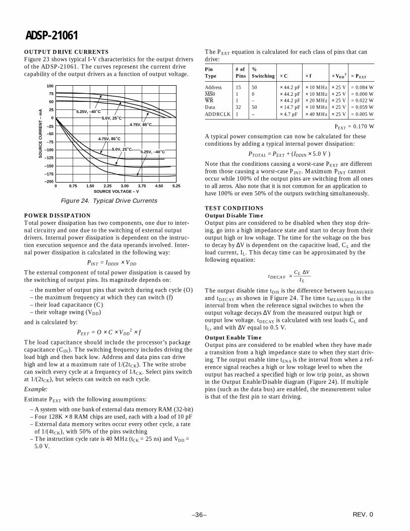
–36–
ADSP-21061
REV. 0
OUTPUT DRIVE CURRENTSFigure 23 shows typical I-V characteristics for the output driversof the ADSP-21061. The curves represent the current drivecapability of the output drivers as a function of output voltage.
SOURCE VOLTAGE – V
100
–75
–150
0 5.25
SO
UR
CE
CU
RR
EN
T –
mA
0.75 1.50 2.25 3.00 3.75 4.50
75
–50
–100
–125
25
–25
50
0
–175
–200
4.75V, 85°C
5.0V, 25°C5.25V, –40°C
4.75V, 85°C
5.0V, 25°C
5.25V, –40°C
Figure 24. Typical Drive Currents
POWER DISSIPATIONTotal power dissipation has two components, one due to inter-nal circuitry and one due to the switching of external outputdrivers. Internal power dissipation is dependent on the instruc-tion execution sequence and the data operands involved. Inter-nal power dissipation is calculated in the following way:
PINT = IDDIN × VDD
The external component of total power dissipation is caused bythe switching of output pins. Its magnitude depends on:
– the number of output pins that switch during each cycle (O)– the maximum frequency at which they can switch (f)– their load capacitance (C)– their voltage swing (VDD)
and is calculated by:
PEXT = O × C × VDD2 × f
The load capacitance should include the processor’s packagecapacitance (CIN). The switching frequency includes driving theload high and then back low. Address and data pins can drivehigh and low at a maximum rate of 1/(2tCK). The write strobecan switch every cycle at a frequency of 1/tCK. Select pins switchat 1/(2tCK), but selects can switch on each cycle.
Example:
Estimate PEXT with the following assumptions:
– A system with one bank of external data memory RAM (32-bit)– Four 128K × 8 RAM chips are used, each with a load of 10 pF– External data memory writes occur every other cycle, a rate of 1/(4tCK), with 50% of the pins switching
– The instruction cycle rate is 40 MHz (tCK = 25 ns) and VDD = 5.0 V.
The PEXT equation is calculated for each class of pins that candrive:
Pin # of %Type Pins Switching × C × f × VDD
2 = PEXT
Address 15 50 × 44.2 pF × 10 MHz × 25 V = 0.084 WMS0 1 0 × 44.2 pF × 10 MHz × 25 V = 0.000 WWR 1 – × 44.2 pF × 20 MHz × 25 V = 0.022 WData 32 50 × 14.7 pF × 10 MHz × 25 V = 0.059 WADDRCLK 1 – × 4.7 pF × 40 MHz × 25 V = 0.005 W
PEXT = 0.170 W
A typical power consumption can now be calculated for theseconditions by adding a typical internal power dissipation:
PTOTAL = PEXT + (IDDIN × 5.0 V )
Note that the conditions causing a worst-case PEXT are differentfrom those causing a worst-case PINT. Maximum PINT cannotoccur while 100% of the output pins are switching from all onesto all zeros. Also note that it is not common for an application tohave 100% or even 50% of the outputs switching simultaneously.
TEST CONDITIONSOutput Disable TimeOutput pins are considered to be disabled when they stop driv-ing, go into a high impedance state and start to decay from theiroutput high or low voltage. The time for the voltage on the busto decay by ∆V is dependent on the capacitive load, CL and theload current, IL. This decay time can be approximated by thefollowing equation:
tDECAY =
CL ∆VIL
The output disable time tDIS is the difference between tMEASURED
and tDECAY as shown in Figure 24. The time tMEASURED is theinterval from when the reference signal switches to when theoutput voltage decays ∆V from the measured output high oroutput low voltage. tDECAY is calculated with test loads CL andIL, and with ∆V equal to 0.5 V.
Output Enable TimeOutput pins are considered to be enabled when they have madea transition from a high impedance state to when they start driv-ing. The output enable time tENA is the interval from when a ref-erence signal reaches a high or low voltage level to when theoutput has reached a specified high or low trip point, as shownin the Output Enable/Disable diagram (Figure 24). If multiplepins (such as the data bus) are enabled, the measurement valueis that of the first pin to start driving.

ADSP-21061
–37–REV. 0
System Hold Time CalculationTo determine the data output hold time in a particular system,first calculate tDECAY using the equation given above. Choose ∆Vto be the difference between the ADSP-21061’s output voltageand the input threshold for the device requiring the hold time. Atypical ∆V will be 0.4 V. CL is the total bus capacitance (perdata line), and IL is the total leakage or three-state current (perdata line). The hold time will be tDECAY plus the minimum dis-able time (i.e., tDATRWH for the write cycle).
REFERENCESIGNAL
tDIS
OUTPUT STARTSDRIVING
VOH (MEASURED) – ∆V
VOL (MEASURED) + ∆V
tMEASURED
VOH (MEASURED)
VOL (MEASURED)
2.0V
1.0V
VOH (MEASURED)
VOL (MEASURED)
HIGH-IMPEDANCE STATE.TEST CONDITIONS CAUSETHIS VOLTAGE TO BEAPPROXIMATELY 1.5V
OUTPUT STOPSDRIVING
tENA
tDECAY
OUTPUT
Figure 25. Output Enable/Disable
+1.5V
50pF
TOOUTPUT
PIN
IOL
IOH
Figure 26. Equivalent Device Loading for AC Measure-ments (Includes All Fixtures)
INPUT OROUTPUT 1.5V1.5V
Figure 27. Voltage Reference Levels for AC Measure-ments (Except Output Enable/Disable)
Capacitive LoadingOutput delays and holds are based on standard capacitive loads:50 pF on all pins (see Figure 26). The delay and hold specifica-tions given should be derated by a factor of 1.5 ns/50 pF forloads other than the nominal value of 50 pF. Figures 28 showshow output rise time varies with capacitance. Figure 309 showsgraphically how output delays and holds vary with load capaci-tance. (Note that this graph or derating does not apply to outputdisable delays; see the previous section “Output Disable Time”under “Test Conditions.”) The graphs of Figures 28, 29 and 30may not be linear outside the ranges shown.
LOAD CAPACITANCE – pF
16.0
8.0
00 20020
RIS
E &
FA
LL
TIM
ES
– n
s (0
.5V
– 4
.5V
, 10%
– 9
0%)
40 60 80 100 120 140 160 180
14.0
12.0
4.0
2.0
10.0
6.0
3.7
1.1
14.7
7.4
RISE TIME
FALL TIME
Figure 28. Typical Output Rise Time (10%–90% VDD) vs.Load Capacitance
LOAD CAPACITANCE – pF
3.5
00 20020
RIS
E &
FA
LL
TIM
ES
– n
s (0
.8V
– 2
.0V
)
40 60 80 100 120 140 160 180
3.0
2.5
2.0
1.5
1.0
0.50.6
RISE TIME
FALL TIME
2.9
1.6
Figure 29. Typical Output Rise Time (0.8 V –2.0 V) vs.Load Capacitance
LOAD CAPACITANCE – pF
OU
TP
UT
DE
LA
Y O
R H
OL
D –
ns
5
–125 20050 75 100 125 150 175
4
3
2
1
NOMINAL
–0.7
4.5
Figure 30. Typical Output Delay or Hold vs. Load Capaci-tance (at Maximum Case Temperature) (VDD = 5 V)

–38–
ADSP-21061
REV. 0
ENVIRONMENTAL CONDITIONSThermal CharacteristicsThe ADSP-21061 is packaged in a 240-lead thermally enhancedPQFP. The top surface of the package contains a copper slugfrom which most of the die heat is dissipated. The slug is flushwith the top surface of the package. Note that the copper slug isinternally connected to GND through the device substrate.The ADSP-2106x is specified for a case temperature (TCASE).To ensure that TCASE is not exceeded, a heat sink and/or an airflow source may be used. A heat sink should be attached with athermal adhesive.
TCASE = TAMB + ( PD × θCA )
TCASE = Case temperature (measured on top surface of package)
PD = Power dissipation in W (this value depends upon thespecific application; a method for calculating PD isshown under “Power Dissipation”)
θJA = 0.3°C
Airflow(Linear Ft./Min.) 0 100 200 400 600
θCA (°C/W) 10 4 8 7 6
NOTESThis represents thermal resistance at total power of 5 W. With air flow, no vari-ance is seen in θCA with power.θCA at 0 LFM varies with power: At 2 W, θCA = 14°C/W, at 3 W θCA =11 °C/W.

ADSP-21061
–39–REV. 0
240-LEAD METRIC PQFP PIN CONFIGURATIONS
1
240
60
61 120
121
180
181
TOP VIEW
HEATSLUG
GND
THE 240 LEAD PACKAGE CONTAINS A COPPER HEAT SLUG FLUSH WITHITS TOP SURFACE. THE SLUG IS INTERNALLY CONNECTED TO GROUND.
Pin PinNo. Name
1 TDI2 TRST3 VDD4 TDO5 TIMEXP6 EMU7 ICSA8 FLAG39 FLAG210 FLAG111 FLAG012 GND13 ADDR014 ADDR115 VDD16 ADDR217 ADDR318 ADDR419 GND20 ADDR521 ADDR622 ADDR723 VDD24 ADDR825 ADDR926 ADDR1027 GND28 ADDR1129 ADDR1230 ADDR1331 VDD32 ADDR1433 ADDR1534 GND35 ADDR1636 ADDR1737 ADDR1838 VDD39 VDD40 ADDR19
Pin PinNo. Name
121 DATA41122 DATA40123 DATA39124 VDD125 DATA38126 DATA37127 DATA36128 GND129 NC130 DATA35131 DATA34132 DATA33133 VDD134 VDD135 GND136 DATA32137 DATA31138 DATA30139 GND140 DATA29141 DATA28142 DATA27143 VDD144 VDD145 DATA26146 DATA25147 DATA24148 GND149 DATA23150 DATA22151 DATA21152 VDD153 DATA20154 DATA19155 DATA18156 GND157 DATA17158 DATA16159 DATA15160 VDD
Pin PinNo. Name
81 TCLK082 TFS083 DR084 RCLK085 RFS086 VDD87 VDD88 GND89 ADRCLK90 REDY91 HBG92 CS93 RD94 WR95 GND96 VDD97 GND98 CLKIN99 ACK100 DMAG2101 DMAG1102 PAGE103 VDD104 BR6105 BR5106 BR4107 BR3108 BR2109 BR1110 GND111 VDD112 GND113 DATA47114 DATA46115 DATA45116 VDD117 DATA44118 DATA43119 DATA42120 GND
Pin PinNo. Name
201 NC202 NC203 NC204 NC205 VDD206 NC207 NC208 NC209 NC210 NC211 NC212 GND213 NC214 NC215 NC216 NC217 NC218 NC219 VDD220 GND221 VDD222 NC223 NC224 NC225 NC226 NC227 NC228 GND229 ID2230 ID1231 ID0232 LBOOT233 RPBA234 RESET235 EBOOT236 IRQ2237 IRQ1238 IRQ0239 TCK240 TMS
Pin PinNo. Name
161 DATA14162 DATA13163 DATA12164 GND165 DATA11166 DATA10167 DATA9168 VDD169 DATA8170 DATA7171 DATA6172 GND173 DATA5174 DATA4175 DATA3176 VDD177 DATA2178 DATA1179 DATA0180 GND181 GND182 NC183 NC184 NC185 NC186 NC187 NC188 VDD189 NC190 NC191 NC192 NC193 NC194 NC195 GND196 GND197 VDD198 NC199 NC200 NC
Pin PinNo. Name
41 ADDR2042 ADDR2143 GND44 ADDR2245 ADDR2346 ADDR2447 VDD48 GND49 VDD50 ADDR2551 ADDR2652 ADDR2753 GND54 MS355 MS256 MS157 MS058 SW59 BMS60 ADDR2861 GND62 VDD63 VDD64 ADDR2965 ADDR3066 ADDR3167 GND68 SBTS69 DMAR270 DMAR171 HBR72 DT173 TCLK174 TFS175 DR176 RCLK177 RFS178 GND79 CPA80 DT0

–40–
ADSP-21061
REV. 0
PACKAGE DIMENSIONSDimensions shown in inches and (mm).
240-Lead Metric PQFP
1
181
180
121
12061
60
GND
HEATSLUG
THE THERMALLY ENHANCED PQFP PACKAGE CONTAINS ACOPPER HEAT SLUG FLUSH WITH ITS TOP SURFACE; THESLUG IS INTERNALLY CONNECTED TO GROUND. THE HEATSLUG DIAMETER IS 24.1 (0.949) mm.
240 LEAD METRIC PQFPTOP VIEW (PINS DOWN)
1.372 (34.85) 1.362 (34.60) TYP SQ 1.352 (34.35)
1.264 (32.10) 1.260 (32.00) TYP SQ 1.256 (31.90)
1.165 (29.60) 1.161 (29.50) TYP SQ 1.157 (29.40)
240
INCHES (MILLIMETERS)
SEATINGPLANE
0.161 (4.10)MAX
0.030 (0.75) 0.024 (0.60) TYP 0.020 (0.50)
0.004 (0.10)MAX
0.010 (0.25)MIN
0.138 (3.50) 0.134 (3.40) TYP 0.130 (3.30)
0.011 (0.27) 0.009 (0.22) TYP 0.007 (0.17)
LEAD PITCH0.01969 (0.50)
TYP
LEAD WIDTH
NOTE:THE ACTUAL POSITION OF EACH LEAD IS WITHIN (0.08)0.0032 FROM ITS IDEAL POSITION WHEN MEASURED IN THELATERAL DIRECTION.CENTER FIGURES ARE TYPICAL UNLESS OTHERWISE NOTED
C31
36–5
–7/9
7P
RIN
TE
D IN
U.S
.A.
ORDERING GUIDE
Part Number* Case Temperature Range Instruction Rate On-Chip SRAM Operating Voltage
ADSP-21061KS-133 0°C to +85°C 33 MHz 1 Mbit 5 VADSP-21061KS-160 0°C to +85°C 40 MHz 1 Mbit 5 VADSP-21061KS-200x 0°C to +85°C 50 MHz 1 Mbit 5 V