adt7462 - flexible temperature and voltage monitor and
TRANSCRIPT

© Semiconductor Components Industries, LLC, 2016
January, 2016 − Rev. 51 Publication Order Number:
ADT7462/D
ADT7462
Flexible Temperature,Voltage Monitor, andSystem Fan Controller
The ADT7462 is a flexible systems monitor IC, suitable for use in awide variety of applications. It can monitor temperature in up to threeremote locations, as well as its ambient temperature.
There are up to four PWM outputs. These can be used to control thespeed of a cooling fan by varying the % duty cycle of the PWM drivesignal applied to the fan. The ADT7462 supports high frequencyPWM for 4-wire fans and low frequency PWM for 2-wire and 3-wirefans. Up to eight TACH inputs can be used to measure the speed of3-wire and 4-wire fans. There are up to 13 voltage monitoring inputs,ranging from 12 V to 0.9 V.
The ADT7462 is fully compatible with SMBus 1.1 and SMBus 1.0.The ADT7462 also includes a THERM I/O and a RESET I/O.
The ADT7462 is available in a 32-lead LFCSP_VQ. Many of thepins are multi-functional. Five easy configuration options can be setup using the easy configuration register. Users choose theconfiguration closest to their requirements; individual pins can bereconfigured after the easy configuration option has been chosen.
Features
• One Local and Up to Three Remote Temperature Channels SeriesResistance Cancellation On Remote Channels
• Thermal Protection Using THERM Pins
• Up to Four PWM Fan Drive Outputs Supports Both High andLow Frequency PWM Drives
• Up to Eight TACH Inputs Measures the Speed of 3-wire and4-wire Fans
• Automatic Fan Speed Control Loop Includes Dynamic TMIN Control
• Monitors Up to 13 V Inputs
• Monitors Up to 7 VID Inputs; Includes On-The-Fly (OTF)VID Support
• Bidirectional Reset
• Chassis Intrusion Detect
• SMBus 1.1 and SMBus 1.0 Compatible
• 3.3 V and 5.0 V Operation
• Extended Operating Range from −40°C to +125°C
• Space-saving 32-lead Chip Scale Package
• This is a Pb-Free Device*
Applications
• Servers and Personal Computers
• Telecommunications Equipment
• Test Equipment and Measurement Instruments
*For additional information on our Pb-Free strategy and soldering details, pleasedownload the ON Semiconductor Soldering and Mounting TechniquesReference Manual, SOLDERRM/D.
www.onsemi.com
See detailed ordering and shipping information in the packagedimensions section on page 81 of this data sheet.
ORDERING INFORMATION
MARKING DIAGRAM
PIN ASSIGNMENT
ADT7462ACPZ = Specific Device Code# = Pb-Free PackageYYWW = Date CodeAL = Assembly LotCC = Country Code
ADT7462ACPZ#YYWW
ALCCCCC
LFCSP−32CASE 932
PIN 1INDICATOR
1VID0/GPIO1/TACH1
2VID1/GPIO2/TACH2
3VID2/GPIO3/TACH3
4VID3/GPIO4/TACH4
5V CC
6GND
7TACH5/+12V1
8TACH6/+12V2
24
VCCP2/
23VCCP1/
22 TACH8/+12V3
21 TACH7/+5V
20 D3–/SCSI_TERM2
19 D3+/+1.25V/+0.9V
18 D2–
17 D2+9
SC
L
10S
DA
11A
DD
12A
LE
RT
13P
WM
4/+3
.3V
14R
ES
ET
15D
1+/+
2.5V
/+1.
8V
16D
1–/S
CS
I_T
ER
M1
32V
ID5/
GP
IO6/
PW
M2
31V
ID4/
GP
IO5/
PW
M1
30P
WM
3
29T
HE
RM
2/+1
.5V
2/G
PIO
8
28T
HE
RM
1/+1
.5V
1/G
PIO
7/V
ID6
27FA
N2M
AX
/CI
26V
R_H
OT
2/+1
.2V
2/V
BA
TT
25
ADT7462
VR
_HO
T1/
+1.2
V1/
+3.3
V
+1.5V/+1.8V/+2.5V
+1.5V/+1.8V/+2.5V

ADT7462
www.onsemi.com2
Figure 1. Functional Block Diagram
SMBusADDRESS
SELECTION
SERIAL BUSINTERFACE
VIDREGISTER
PWM REGISTERS
PERFORMANCEMONITORING
THERMALPROTECTION
INPUT SIGNALCONDITIONINGAND ANALOGMULTIPLEXER
BAND GAPTEMPERATURE
SENSOR
VID0 TO VID6
PWM1 TO PWM4
TACH1 TO TACH8
VR_HOT2VR_HOT1THERM2
THERMAL DIODE INPUTSVOLTAGE INPUTS
ADT7462
AUTOMATICFAN SPEEDCONTROL
ACOUSTICENHANCEMENT
CONTROL
DYNAMIC TMINCONTROL
13−BITADC
BAND GAPREFERENCE
GPIO1 TO GPIO8
RESET
CI
GND
ADD SCL SDA ALERT
FAN SPEEDCOUNTER
FAN2MAX
THERM1
SCSI_TERM1 ANDSCSI_TERM2
ADDRESS POINTERREGISTER
PWMCONFIGURATION
REGISTERS
INTERRUPTMASKING
RESETCIRCUIT
GPIO STATUS ANDCONFIGURATION
REGISTERS
VALUE AND LIMITREGISTERS
LIMITCOMPARATORS
INTERRUPTSTATUS
REGISTERS
SCSI STATUS
Table 1. ABSOLUTE MAXIMUM RATINGS
Parameter Rating Unit
Supply Voltage 6.5 V
Voltage on +12V Pin 20 V
Voltage on VBATT Pin 4.0 V
Voltage on Any Other Input or Output Pin −0.3 to +6.5 V
Input Current at Any Pin ±5 mA
Package Input Current ±20 mA
Maximum Junction Temperature (TJ MAX) 150 °C
Operating Temperature Range −40 to +125 °C
Storage Temperature Range −65 to +150 °C
Lead Temperature, SolderingLead Temperature (Soldering, 10 sec)IR Reflow Peak Temperature
300260
°C
ESD Rating 1500 V
Stresses exceeding those listed in the Maximum Ratings table may damage the device. If any of these limits are exceeded, device functionalityshould not be assumed, damage may occur and reliability may be affected.
NOTE: This device is ESD sensitive. Use standard ESD precautions when handling.
Table 2. THERMAL CHARACTERISTICS
Package Type �JA �JC Unit
32-lead LFCSP_VQ 32.5 32.71 °C/W
1. �JA is specified for the worst-case conditions, that is, a device soldered in a circuit board for surface-mount packages.

ADT7462
www.onsemi.com3
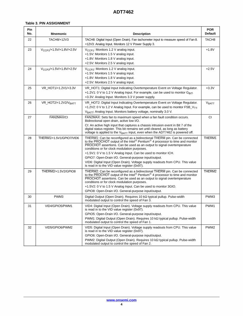
Table 3. PIN ASSIGNMENT
PinNo. Mnemonic Description
PORDefault
1 VID0/GPIO1/TACH1 VID0: Digital Input (Open Drain). Voltage supply readouts from CPU. This valueis read in to the VID value register (0x97).GPIO1: Open-Drain I/O. General-purpose input/output.TACH1: Digital Input (Open Drain). Fan tachometer input to measure speed of Fan 1.
TACH1
2 VID1/GPIO2/TACH2 VID1: Digital Input (Open Drain). Voltage supply readouts from CPU. This valueis read in to the VID value register (0x97).GPIO2: Open-Drain I/O. General-purpose input/output.TACH2: Digital Input (Open Drain). Fan tachometer input to measure speed of Fan 2.
TACH2
3 VID2/GPIO3/TACH3 VID2: Digital Input (Open Drain). Voltage supply readouts from CPU. This valueis read in to the VID value register (0x97).GPIO3: Open-Drain I/O. General-purpose input/output.TACH3: Digital Input (Open Drain). Fan tachometer input to measure speed of Fan 3.
TACH3
4 VID3/GPIO4/TACH4 VID3: Digital Input (Open Drain). Voltage supply readouts from CPU. This valueis read in to the VID value register (0x97).GPIO4: Open-Drain I/O. General-purpose input/output.TACH4: Digital Input (Open Drain). Fan tachometer input to measure speed of Fan 4.
TACH4
5 VCC Power Supply. Can be powered by 3.3 V standby if monitoring in low powerstates is required. The ADT7462 can also be powered from a 5.0 V supply.
VCC
6 GND Ground Pin. GND
7 TACH5/+12V1 TACH5: Digital Input (Open Drain). Fan tachometer input to measure speed of Fan 5.+12V1: Analog Input. Monitors 12 V Power Supply 1. Attenuators switched on bydefault.
TACH5
8 TACH6/+12V2 TACH6: Digital Input (Open Drain). Fan tachometer input to measure speed of Fan 6.+12V2: Analog Input. Monitors 12 V Power Supply 2. Attenuators switched on bydefault.
TACH6
9 SCL Digital Input (Open Drain). SMBus serial clock input. Requires SMBus pullup. SCL
10 SDA Digital I/O (Open Drain). SMBus bidirectional serial data. Requires SMBuspullup.
SDA
11 ADD The state of this pin on powerup determines the SMBus device address. ADD
12 ALERT Active Low Open-Drain Digital Output. Requires 10 k� typical pullup. TheALERT pin is used to signal out-of-limit comparisons of temperature, voltage,and fan speed. This is compatible with SMBus ALERT.
ALERT
13 PWM4/+3.3V PWM4: Digital Output (Open Drain). Requires 10 k� typical pullup. Pulse-widthmodulated output to control the speed of Fan 4.+3.3V: Analog Input. Monitors 3.3 V power supply.
PWM4
14 RESET Active Low Open-Drain Digital I/O. Power-on reset, 5 mA driver (weak 100 k�pullup), active low output (100 k� pullup) with a 180 ms typical pulse width.RESET is asserted whenever VCC is below the reset threshold. It remainsasserted for approximately 180 ms after VCC rises above the reset threshold.Pin 14 also functions as an active low RESET input and resets all unlockedregisters to their default values.
RESET
15 D1+/+2.5V/+1.8V D1+: Anode Connection to Thermal Diode 1.+2.5V: Monitors 2.5 V analog input.+1.8V: Monitors 1.8 V analog input.
D1+
16 D1−/SCSI_TERM1 D1−: Cathode Connection to Thermal Diode 1.SCSI_TERM1: Digital Input, SCSI Termination 1.
D1−
17 D2+ Anode Connection to Thermal Diode 2. D2+
18 D2− Cathode Connection to Thermal Diode 2. D2−
19 D3+/+1.25V/+0.9V D3+: Anode Connection to Thermal Diode 3.+1.25V: Monitors 1.25 V analog input.+0.9V: Monitors 0.9 V analog input.
D3+
20 D3−/SCSI_TERM2 D3−: Cathode connection to Thermal Diode 3.SCSI_TERM2: Digital Input, SCSI Termination 2.
D3−
21 TACH7/+5V TACH7: Digital Input (Open Drain). Fan tachometer input to measure speed of Fan 7.+5V: Analog Input. Monitors 5.0 V power supply.
TACH7
ADT7462
www.onsemi.com4
Table 3. PIN ASSIGNMENT
PinNo.
PORDefaultDescriptionMnemonic
22 TACH8/+12V3 TACH8: Digital Input (Open Drain). Fan tachometer input to measure speed of Fan 8.+12V3: Analog Input. Monitors 12 V Power Supply 3.
TACH8
23 VCCP1/+1.5V/+1.8V/+2.5V VCCP1: Monitors 1.2 V analog input.+1.5V: Monitors 1.5 V analog input.+1.8V: Monitors 1.8 V analog input.+2.5V: Monitors 2.5 V analog input.
+1.8V
24 VCCP2/+1.5V/+1.8V/+2.5V VCCP2: Monitors 1.2 V analog input.+1.5V: Monitors 1.5 V analog input.+1.8V: Monitors 1.8 V analog input.+2.5V: Monitors 2.5 V analog input.
+2.5V
25 VR_HOT1/+1.2V1/+3.3V VR_HOT1: Digital Input Indicating Overtemperature Event on Voltage Regulator.+1.2V1: 0 V to 1.2 V Analog Input. For example, can be used to monitor GBIT.+3.3V: Analog Input. Monitors 3.3 V power supply.
+3.3V
26 VR_HOT2/+1.2V2/VBATT VR_HOT2: Digital Input Indicating Overtemperature Event on Voltage Regulator.+1.2V2: 0 V to 1.2 V Analog Input. For example, can be used to monitor FSB_VTT.VBATT: Analog Input. Monitors battery voltage, nominally 3.0 V.
VBATT
27 FAN2MAX/CI FAN2MAX: Sets fan to maximum speed when a fan fault condition occurs.Bidirectional open drain, active low I/O.CI: An active high input that captures a chassis intrusion event in Bit 7 of thedigital status register. This bit remains set until cleared, as long as batteryvoltage is applied to the VBATT input, even when the ADT7462 is powered off.
CI
28 THERM1/+1.5V1/GPIO7/VID6 THERM1: Can be reconfigured as a bidirectional THERM pin. Can be connectedto the PROCHOT output of the Intel® Pentium® 4 processor to time and monitorPROCHOT assertions. Can be used as an output to signal overtemperatureconditions or for clock modulation purposes.+1.5V1: 0 V to 1.5 V Analog Input. Can be used to monitor ICH.GPIO7: Open-Drain I/O. General-purpose input/output.VID6: Digital Input (Open Drain). Voltage supply readouts from CPU. This valueis read in to the VID value register (0x97).
THERM1
29 THERM2/+1.5V2/GPIO8 THERM2: Can be reconfigured as a bidirectional THERM pin. Can be connectedto the PROCHOT output of the Intel® Pentium® 4 processor to time and monitorPROCHOT assertions. Can be used as an output to signal overtemperatureconditions or for clock modulation purposes.+1.5V2: 0 V to 1.5 V Analog Input. Can be used to monitor 3GIO.GPIO8: Open-Drain I/O. General-purpose input/output.
THERM2
30 PWM3 Digital Output (Open Drain). Requires 10 k� typical pullup. Pulse-widthmodulated output to control the speed of Fan 3.
PWM3
31 VID4/GPIO5/PWM1 VID4: Digital Input (Open Drain). Voltage supply readouts from CPU. This valueis read in to the VID value register (0x97).GPIO5: Open-Drain I/O. General-purpose input/output.PWM1: Digital Output (Open Drain). Requires 10 k� typical pullup. Pulse-widthmodulated output to control the speed of Fan 1.
PWM1
32 VID5/GPIO6/PWM2 VID5: Digital Input (Open Drain). Voltage supply readouts from CPU. This valueis read in to the VID value register (0x97).GPIO6: Open-Drain I/O. General-purpose input/output.PWM2: Digital Output (Open Drain). Requires 10 k� typical pullup. Pulse-widthmodulated output to control the speed of Fan 2.
PWM2
ADT7462
www.onsemi.com5
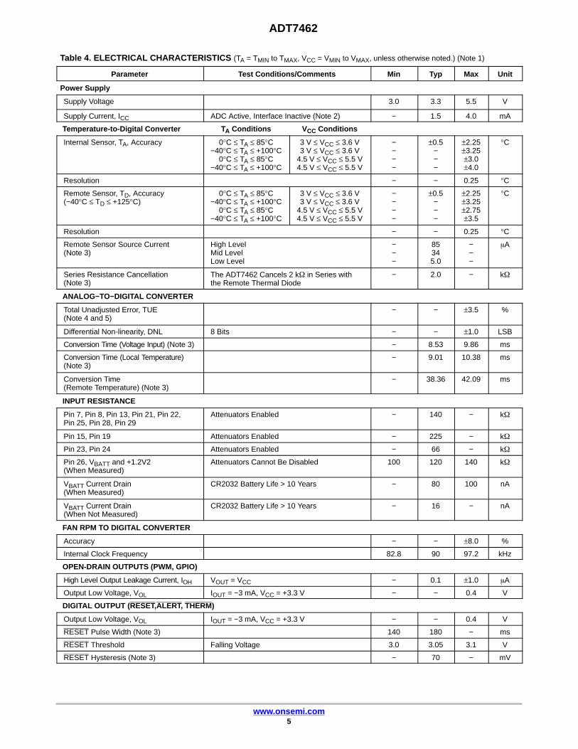
Table 4. ELECTRICAL CHARACTERISTICS (TA = TMIN to TMAX, VCC = VMIN to VMAX, unless otherwise noted.) (Note 1)
Parameter Test Conditions/Comments Min Typ Max Unit
Power Supply
Supply Voltage 3.0 3.3 5.5 V
Supply Current, ICC ADC Active, Interface Inactive (Note 2) − 1.5 4.0 mA
Temperature-to-Digital Converter TA Conditions VCC Conditions
Internal Sensor, TA, Accuracy 0°C ≤ TA ≤ 85°C−40°C ≤ TA ≤ +100°C
0°C ≤ TA ≤ 85°C−40°C ≤ TA ≤ +100°C
3 V ≤ VCC ≤ 3.6 V3 V ≤ VCC ≤ 3.6 V
4.5 V ≤ VCC ≤ 5.5 V4.5 V ≤ VCC ≤ 5.5 V
−−−−
±0.5−−−
±2.25±3.25±3.0±4.0
°C
Resolution − − 0.25 °C
Remote Sensor, TD, Accuracy(−40°C ≤ TD ≤ +125°C)
0°C ≤ TA ≤ 85°C−40°C ≤ TA ≤ +100°C
0°C ≤ TA ≤ 85°C−40°C ≤ TA ≤ +100°C
3 V ≤ VCC ≤ 3.6 V3 V ≤ VCC ≤ 3.6 V
4.5 V ≤ VCC ≤ 5.5 V4.5 V ≤ VCC ≤ 5.5 V
−−−−
±0.5−−−
±2.25±3.25±2.75±3.5
°C
Resolution − − 0.25 °C
Remote Sensor Source Current(Note 3)
High LevelMid LevelLow Level
−−−
85345.0
−−−
�A
Series Resistance Cancellation(Note 3)
The ADT7462 Cancels 2 k� in Series withthe Remote Thermal Diode
− 2.0 − k�
ANALOG−TO−DIGITAL CONVERTER
Total Unadjusted Error, TUE(Note 4 and 5)
− − ±3.5 %
Differential Non-linearity, DNL 8 Bits − − ±1.0 LSB
Conversion Time (Voltage Input) (Note 3) − 8.53 9.86 ms
Conversion Time (Local Temperature)(Note 3)
− 9.01 10.38 ms
Conversion Time(Remote Temperature) (Note 3)
− 38.36 42.09 ms
INPUT RESISTANCE
Pin 7, Pin 8, Pin 13, Pin 21, Pin 22,Pin 25, Pin 28, Pin 29
Attenuators Enabled − 140 − k�
Pin 15, Pin 19 Attenuators Enabled − 225 − k�
Pin 23, Pin 24 Attenuators Enabled − 66 − k�
Pin 26, VBATT and +1.2V2(When Measured)
Attenuators Cannot Be Disabled 100 120 140 k�
VBATT Current Drain(When Measured)
CR2032 Battery Life > 10 Years − 80 100 nA
VBATT Current Drain(When Not Measured)
CR2032 Battery Life > 10 Years − 16 − nA
FAN RPM TO DIGITAL CONVERTER
Accuracy − − ±8.0 %
Internal Clock Frequency 82.8 90 97.2 kHz
OPEN-DRAIN OUTPUTS (PWM, GPIO)
High Level Output Leakage Current, IOH VOUT = VCC − 0.1 ±1.0 �A
Output Low Voltage, VOL IOUT = −3 mA, VCC = +3.3 V − − 0.4 V
DIGITAL OUTPUT (RESET,ALERT, THERM)
Output Low Voltage, VOL IOUT = −3 mA, VCC = +3.3 V − − 0.4 V
RESET Pulse Width (Note 3) 140 180 − ms
RESET Threshold Falling Voltage 3.0 3.05 3.1 V
RESET Hysteresis (Note 3) − 70 − mV

ADT7462
www.onsemi.com6
Table 4. ELECTRICAL CHARACTERISTICS (TA = TMIN to TMAX, VCC = VMIN to VMAX, unless otherwise noted.) (Note 1)
Parameter UnitMaxTypMinTest Conditions/Comments
OPEN-DRAIN SERIAL BUS OUTPUT (SDA)
Output Low Voltage, VOL IOUT = −3 mA, VCC = +3.3 V − − 0.4 V
High Level Output Leakage Current, IOH VOUT = VCC − 0.1 ±1.0 �A
SERIAL BUS DIGITAL INPUTS (SDA AND SCL)
Input High Voltage, VIH 2.1 − − V
Input Low Voltage, VIL − − 0.8 V
Hysteresis − 500 − mV
DIGITAL INPUT LOGIC LEVELS (VID0 to VID6) AND THERM, TACH, GPIO, VR_HOT, SCSI_TERM)
Input High Voltage, VIH Bit 3 and Bit 4 of Configuration Register 3 = 0 1.7 − − V
Input Low Voltage, VIL Bit 3 and Bit 4 of Configuration Register 3 = 0 − − 0.8 V
Input High Voltage, VIH (VID0 to VID6) Bit 3 of Configuration Register 3 = 1 0.65 − − V
Input High Voltage, VIH (THERM) Bit 4 of Configuration Register 3 = 1 2/3 VCCP1 − − V
Input Low Voltage, VIL Bit 3 and Bit 4 of Configuration Register 3 = 1 − − 0.4 V
Hysteresis − 500 − mV
DIGITAL INPUT CURRENTS
Input High Current, IIH VIN = VCC −1.0 − − �A
Input Low Current, IIL VIN = 0 − − +1.0 �A
Input Capacitance (Note 3) − 5.0 − pF
SERIAL BUS TIMING (Note 3)
Clock Frequency See Figure 2 − − 400 kHz
Glitch Immunity, tSW See Figure 2 − 50 − ns
Bus Free Time See Figure 2 1.3 − − �s
Start Setup Time, tSU;STA See Figure 2 0.6 − − �s
Start Hold Time, tHD;STA See Figure 2 0.6 − − �s
SCL Low Time, tLOW See Figure 2 1.3 − − �s
SCL High Time, tHIGH See Figure 2 0.6 − − �s
SCL, SDA Rise Time, tR See Figure 2 − − 1000 ns
SCL, SDA Fall Time, tF See Figure 2 − − 300 ns
Data Setup Time, tSU;DAT See Figure 2 100 − − ns
Detect Clock Low Timeout Can Be Optionally Enabled − 25 − ms
1. All voltages are measured with respect to GND, unless otherwise specified. Typical values are at TA = 25°C and represent the most likelyparametric norm. Logic inputs accept input high voltages up to 5.0 V, even when the device is operating at supply voltages below 5.0 V. Timingspecifications are tested at logic levels of VIL = 0.8 V for a falling edge and VIH = 2.0 V for a rising edge.
2. Unused digital inputs connected to GND.3. Guaranteed by design, not production tested.4. Note that this specification does not apply if Pin 26 (VBATT, +1.2V) is being measured in single-channel mode. See Figure 16 in the Typical
Performance Characteristics section for VBATT accuracy.5. For Pin 23 and Pin 24 configured as +1.8V or +2.5V only, restricted conditions of VCC ≥ 3.3 V and +25°C ≤ TA ≤ +125°C apply.
Figure 2. Serial Bus Timing Diagram
PS
tSU; DAT
tHIGH
tF
tHD; DAT
tR
tLOW
tSU; STO
P S
SCL
SDA
tBUF
tHD; STA
tHD; STA
tSU; STA

ADT7462
www.onsemi.com7
TYPICAL PERFORMANCE CHARACTERISTICS
Figure 3. Supply Current vs. Supply Voltage Figure 4. Supply Current vs. Temperature
Figure 5. Local Sensor Temperature Error Figure 6. Remote Sensor Temperature Error
Figure 7. Temperature Error Measuring IntelPentium� 4 Processor
Figure 8. ADT7462 Response to Thermal Shock
SUPPLY VOLTAGE (V)
2.90.00125
I DD
(A
mps
)
3.4 3.9 4.4 4.9 5.4
0.00130
0.00135
0.00140
0.00145
0.00150
0.00155
0.00160
DEV1
DEV3
DEV2
TEMPERATURE (°C)
−450.00122
I DD
(A
mps
)
DEV1
DEV3
DEV2
5 55 105
0.00124
0.00126
0.00128
0.00130
0.00132
0.00134
0.00136
0.00138
0.00140
0.00142
0.00144
TEMPERATURE (°C)
−40
TE
MP
ER
AT
UR
E E
RR
OR
(°C
)
−1−20 0 20 40 60 80 100 120
0
1
2
VCC = 5.5 V
VCC = 3.3 V
TEMPERATURE (°C)
−40
TE
MP
ER
AT
UR
E E
RR
OR
(°C
)
−1−20 0 20 40 60 80 100 120
0
1
2
VCC = 5.5 V
VCC = 3.3 V
TEMPERATURE (°C)
−40
TE
MP
ER
AT
UR
E E
RR
OR
(°C
)
−4−20 0 20 40 60 80 100 120
−3
−2
−1
0
1
2
3
4
5
TIME (Seconds)
0
TE
MP
ER
AT
UR
E R
EA
DIN
G (
°C)
020 40 60 80 100 120
20
40
60
80
100
120
140
INTEXT1EXT2EXT3
MEANLO SPEC
HI SPEC
2015105191494181383171272161161

ADT7462
www.onsemi.com8
TYPICAL PERFORMANCE CHARACTERISTICS (Cont’d)
Figure 9. Remote Temperature Error vs.Resistance (SRC)
Figure 10. Local Temperature Error vs. PowerSupply Noise Frequency
Figure 11. Remote Temperature Error vs. PowerSupply Noise Frequency
Figure 12. Remote Temperature Error vs.Common-Mode Noise Frequency
Figure 13. Remote Temperature Error vs.Differential-Mode Noise Frequency
Figure 14. Remote Temperature Error vs.Capacitance Between D+ and D−
RESISTANCE (M�)
0
TE
MP
ER
AT
UR
E E
RR
OR
(°C
)
−60
D+ To VCC
D+ To GND
20 40 60 80 100
−40
−20
0
20
40
60
POWER SUPPLY NOISE FREQUENCY (kHz)
10
TE
MP
ER
AT
UR
E E
RR
OR
(°C
)
−20
50 mV
100 1M 10M 100M 1G
−15
−10
−5
0
5
10
15
125 mV
POWER SUPPLY NOISE FREQUENCY (kHz)
10
TE
MP
ER
AT
UR
E E
RR
OR
(°C
)
−12
50 mV
100 1M 10M 100M 1G
−10
−8
−6
−4
−2
0
2
125 mV4
6
8
NOISE FREQUENCY (kHz)
10
TE
MP
ER
AT
UR
E E
RR
OR
(°C
)
−10100 1M 10M 100M 1G
−5
0
5
10
15
20
25
100 mV
40 mV
60 mV
NOISE FREQUENCY (kHz)
10
TE
MP
ER
AT
UR
E E
RR
OR
(°C
)
−1
10 mV
100 1M 10M 100M 1G
0
1
2
3
4
5
6
7
20 mV
CAPACITANCE (nF)
0
TE
MP
ER
AT
UR
E E
RR
OR
(°C
)
−502 4 6 8 10
−40
−30
−20
−10
0
10
DEV1, EXT1DEV1, EXT2DEV1, EXT3DEV2, EXT1DEV2, EXT2DEV2, EXT3DEV3, EXT1DEV3, EXT2DEV3, EXT3

ADT7462
www.onsemi.com9
TYPICAL PERFORMANCE CHARACTERISTICS (Cont’d)
Figure 15. Local Temperature vs. Power-On ResetTimeout
Figure 16. Applied Voltage vs. VBATT Reading
Figure 17. TACH Accuracy vs. Supply Voltage Figure 18. TACH Accuracy vs. Temperature
TIMEOUT (Seconds)
−50
TE
MP
ER
AT
UR
E (
°C)
0.1800 50 100 150
0.182
0.184
0.186
0.188
0.190
0.192
0.194
0.196
0.198
0.200
POWERUP
STANDBY
VBATT READING (V)
0
VO
LTA
GE
AP
PLI
ED
TO
VB
AT
T (
V)
0
DEV1
0.5 1.0 1.5 2.0 2.5 3.0
0.5
1.0
1.5
2.0
2.5
3.0
DEV2DEV3
SUPPLY (V)
2.9
TAC
H E
RR
OR
(%
)
0
DEV1DEV2DEV3
3.4 3.9 4.4 4.9 5.4
0.5
1.0
1.5
2.0
2.5
3.0
3.5
4.0
4.5
5.0
TEMPERATURE (°C)
−50
TAC
H E
RR
OR
(%
)
−2.0
DEV1
0 50 100 150
−1.5
−1.0
−0.5
0
0.5
1.0
1.5
DEV3
DEV2

ADT7462
www.onsemi.com10
Function Description: Easy ConfigurationOptions
There are a number of multifunctional pins on theADT7462 that need to be configured on powerup to suit thedesired application. Note that due to the large number of pinsthat need to be configured, it could take several SMBustransactions to achieve the required configuration. For thisreason, the ADT7462 has five easy configuration options.The user sets a bit in the easy configuration option register(0x14) to set up the required configuration (see Table 5).
Table 5. EASY CONFIGURATION REGISTERSETTINGS
Easy Configuration Option Register 0x14 Setting
Option 1 Bit 0 = 1
Option 2 Bit 1 = 1
Option 3 Bit 2 = 1
Option 4 Bit 3 = 1
Option 5 Bit 4 = 1
Once the most convenient easy configuration option hasbeen set, the user can configure any of the pins individually.The setup complete bit (Bit 5 of Register 0x01) must then beset to 1 to indicate that the ADT7462 is configured correctly,and then monitoring of the selected channels begins.
The following is a detailed description of the five easyconfiguration options that are available.
Configuration Option 1Configuration Option 1 is the default configuration. It is
also the most suitable for thermal monitoring, voltagemonitoring, and fan control for single and dual processorsystems. Features of Configuration Option 1 include thefollowing:• One Local and Three Remote Temperature Channels
• Four PWM Drives and Eight TACH Inputs
• Two THERM I/Os
• Voltage Monitoring
• +3.3V
• +2.5V
• +1.8V
• VBATT
• RESET I/O
• CI (Chassis Intrusion) or FAN2MAX
Figure 19 shows the pin configuration when ConfigurationOption 1 is chosen.
Figure 19. Configuration Option 1
PIN 1INDICATOR
1TACH12TACH23TACH34TACH45VCC6GND7TACH58TACH6
24 +2.5V23 +1.8V22 TACH821 TACH720 D3–19 D3+18 D2–17 D2+
9S
CL
10S
DA
11A
DD
12A
LE
RT
13P
WM
414
RE
SE
T15
D1+
16D
1–
32P
WM
231
PW
M1
30P
WM
329
TH
ER
M2
28T
HE
RM
127
CI
26V
BA
TT
25+3
.3V
ADT7462TOP VIEW
(Not to Scale)
Table 6. CONFIGURATION OPTION 1
Pin Function Configuration Register Bit Value
1† TACH1 Pin Configuration Reg 1 Bit 4 = 1
2† TACH2 Pin Configuration Reg 1 Bit 3 = 1
3† TACH3 Pin Configuration Reg 1 Bit 2 = 1
4† TACH4 Pin Configuration Reg 1 Bit 1 = 1
7 TACH5 Pin Configuration Reg 1 Bit 0 = 1
8 TACH6 Pin Configuration Reg 2 Bit 7 = 1
13 PWM4 Pin Configuration Reg 2 Bit 6 = 1
15 D1+ Pin Configuration Reg 1 Bit 6 = 1
16 D1− Pin Configuration Reg 1 Bit 6 = 1
19 D3+ Pin Configuration Reg 1 Bit 5 = 1
20 D3− Pin Configuration Reg 1 Bit 5 = 1
21 TACH7 Pin Configuration Reg 2 Bit 3 = 1
22 TACH8 Pin Configuration Reg 2 Bit 2 = 1
23 +1.8V Pin Configuration Reg 2 Bits [1:0] = 10
24 +2.5V Pin Configuration Reg 3 Bits [7:6] = 01
25 +3.3V Pin Configuration Reg 3 Bits [5:4] = 00
26 VBATT Pin Configuration Reg 3 Bits [3:2] = 00
27 CI Pin Configuration Reg 3 Bit 1 = 1
28† THERM1 Pin Configuration Reg 4 Bits [7:6] = 1×
29 THERM2 Pin Configuration Reg 4 Bits [5:4] = 1×
31† PWM1 Pin Configuration Reg 4 Bit 3 = 1
32† PWM2 Pin Configuration Reg 4 Bit 2 = 1
†If VIDs are selected, these pins are configured as VIDs. To enableVIDs, set Bit 7 of Pin Configuration Register 1 (0x10) = 1.

ADT7462
www.onsemi.com11
Configuration Option 2Configuration Option 2 is used for thermal monitoring
and fan control for Processor 1 and Processor 2 in a dualprocessor system. It can also monitor one set of VIDs, ifrequired. Features of Configuration Option 2 include thefollowing:• One Local and Three Remote Thermal Channels
• Up to Four PWM Drives and Up to Eight TACH Inputs(VID Pins and TACHs/PWMs are Muxed Together)
• Two THERM I/Os
• Two VRD Inputs
• RESET I/O
• Two VCCP Voltage Monitoring Channels
Figure 20 shows the pin configuration when ConfigurationOption 2 is chosen.
Figure 20. Configuration Option 2
PIN 1INDICATOR
1TACH12TACH23TACH34TACH45VCC6GND7TACH58TACH6
24 VCCP223 VCCP122 TACH821 TACH720 D3–19 D3+18 D2–17 D2+
9S
CL
10S
DA
11A
DD
12A
LE
RT
13P
WM
414
RE
SE
T15
D1+
16D
1–
32P
WM
231
PW
M1
30P
WM
329
TH
ER
M2
28T
HE
RM
127
FAN
2MA
X26
VR
_HO
T2
25V
R_H
OT
1
ADT7462TOP VIEW
(Not to Scale)
Table 7. CONFIGURATION OPTION 2
Pin Function Configuration Register Bit Value
1† TACH1 Pin Configuration Reg 1 Bit 4 = 1
2† TACH2 Pin Configuration Reg 1 Bit 3 = 1
3† TACH3 Pin Configuration Reg 1 Bit 2 = 1
4† TACH4 Pin Configuration Reg 1 Bit 1 = 1
7 TACH5 Pin Configuration Reg 1 Bit 0 = 1
8 TACH6 Pin Configuration Reg 2 Bit 7 = 1
13 PWM4 Pin Configuration Reg 2 Bit 6 = 1
15 D1+ Pin Configuration Reg 1 Bit 6 = 1
16 D1− Pin Configuration Reg 1 Bit 6 = 1
19 D3+ Pin Configuration Reg 1 Bit 5 = 1
20 D3− Pin Configuration Reg 1 Bit 5 = 1
21 TACH7 Pin Configuration Reg 2 Bit 3 = 1
22 TACH8 Pin Configuration Reg 2 Bit 2 = 1
23 VCCP1 Pin Configuration Reg 2 Bits [1:0] = 00
24 VCCP2 Pin Configuration Reg 3 Bits [7:6] = 00
25 VR_HOT1 Pin Configuration Reg 3 Bits [5:4] = 1×
26 VR_HOT2 Pin Configuration Reg 3 Bits [3:2] = 1×
27 FAN2MAX Pin Configuration Reg 3 Bit 1 = 0
28† THERM1 Pin Configuration Reg 4 Bits [7:6] = 1×
29 THERM2 Pin Configuration Reg 4 Bits [5:4] = 1×
31† PWM1 Pin Configuration Reg 4 Bit 3 = 1
32† PWM2 Pin Configuration Reg 4 Bit 2 = 1
†If VIDs are selected, these pins are configured as VIDs. To enableVIDs, set Bit 7 of Pin Configuration Register 1 (0x10) = 1.

ADT7462
www.onsemi.com12
Configuration Option 3Configuration Option 3 is used to monitor all the voltages
in the system for Processor 1 and Processor 2. Additionalpins can be configured for fan control, VIDs, or GPIOs, asrequired. Features of Configuration Option 3 include thefollowing:• Up to 13 Different Voltages Monitored
• Three +12V
• +5V
• +3.3V
• +2.5V
• +1.8V
• Two +1.5V
• Two +1.2V (VCCP1, VCCP2)
• 0.9V
• VBATT
• One Local and One Remote Temperature Channels
• Up to Three PWM Drives and Up to Four TACH Inputs
• RESET I/O
Figure 21 shows the pin configuration when ConfigurationOption 3 is chosen.
Figure 21. Configuration Option 3
PIN 1INDICATOR
1TACH12TACH23TACH34TACH45VCC6GND7+12V18+12V2
24 VCCP223 VCCP122 +12V321 +5V20 SCSI_TERM219 +0.9V18 D2–17 D2+
9S
CL
10S
DA
11A
DD
12A
LE
RT
13+3
.3V
14R
ES
ET
15+1
.8V
16S
CS
I_T
ER
M1
32P
WM
231
PW
M1
30P
WM
329
+1.5
V/G
PIO
828
+1.5
V/G
PIO
727
CI
26V
BA
TT
25+1
.2V
ADT7462TOP VIEW
(Not to Scale)
Table 8. CONFIGURATION OPTION 3
Pin Function Configuration Register Bit Value
1† TACH1 Pin Configuration Reg 1 Bit 4 = 1
2† TACH2 Pin Configuration Reg 1 Bit 3 = 1
3† TACH3 Pin Configuration Reg 1 Bit 2 = 1
4† TACH4 Pin Configuration Reg 1 Bit 1 = 1
7 +12V1 Pin Configuration Reg 1 Bit 0 = 0
8 +12V2 Pin Configuration Reg 2 Bit 7 = 0
13 +3.3V Pin Configuration Reg 2 Bit 6 = 0
15 +1.8V Pin Configuration Reg 1 Bit 6 = 0
16 SCSI_TERM1
Pin Configuration Reg 1 Bit 6 = 0
19 +0.9V Pin Configuration Reg 1 Bit 5 = 0
20 SCSI_TERM2
Pin Configuration Reg 1 Bit 5 = 0
21 +5V Pin Configuration Reg 2 Bit 3 = 0
22 +12V3 Pin Configuration Reg 2 Bit 2 = 0
23 VCCP1 Pin Configuration Reg 2 Bits [1:0] = 00
24 VCCP2 Pin Configuration Reg 3 Bits [7:6] = 00
25 +1.2V Pin Configuration Reg 3 Bits [5:4] = 01
26 VBATT Pin Configuration Reg 3 Bits [3:2] = 00
27 CI Pin Configuration Reg 3 Bit 1 = 1
28† +1.5V/GPIO7
Pin Configuration Reg 4 Bits [7:6] = 01
29 +1.5V/GPIO8
Pin Configuration Reg 4 Bits [5:4] = 01
31† PWM1 Pin Configuration Reg 4 Bit 3 = 1
32† PWM2 Pin Configuration Reg 4 Bit 2 = 1
†If VIDs are selected, these pins are configured as VIDs. To enableVIDs, set Bit 7 of Pin Configuration Register 1 (0x10) = 1.

ADT7462
www.onsemi.com13
Configuration Option 4Configuration Option 4 is used to monitor temperature,
voltages, and fans for Processor 1 in a dual processorsystem. Features of Configuration Option 4 include thefollowing:• One Local and Two Remote Temperature Channels
• Up to Four PWM Drives and Six TACH Inputs
• Up to Eight Voltages Monitored
• +12V
• +5V
• +3.3V
• Two +1.5V
• +1.2V (VCCP1)
• +0.984V (Mem_VTT)
• VBATT
• THERM I/O
• VRD Input
• RESET I/O
Figure 22 shows the pin configuration when ConfigurationOption 4 is chosen.
Figure 22. Configuration Option 4
PIN 1INDICATOR
1TACH12TACH23TACH34TACH4
TACH58TACH6
24 +2.5V23 VCCP122 +12V321 +5V20 SCSI_TERM219 +0.9V
9 10 11 12 13P
WM
414 15
D1+
16D
1–
32P
WM
231
PW
M1
30 29T
HE
RM
2/+1
.5V
28T
HE
RM
1/+1
.5V
27FA
N2M
AX
26V
BA
TT
25V
R_H
OT
1
ADT7462TOP VIEW
(Not to Scale)VCC
GND
SC
LS
DA
AD
DA
LE
RT
RE
SE
T
PW
M3
5
6
7 D2−D2+
18
17
Table 9. CONFIGURATION OPTION 4
Pin Function Configuration Register Bit Value
1† TACH1 Pin Configuration Reg 1 Bit 4 = 1
2† TACH2 Pin Configuration Reg 1 Bit 3 = 1
3† TACH3 Pin Configuration Reg 1 Bit 2 = 1
4† TACH4 Pin Configuration Reg 1 Bit 1 = 1
7 TACH5 Pin Configuration Reg 1 Bit 0 = 1
8 TACH6 Pin Configuration Reg 2 Bit 7 = 1
13 PWM4 Pin Configuration Reg 2 Bit 6 = 1
15 D1+ Pin Configuration Reg 1 Bit 6 = 1
16 D1− Pin Configuration Reg 1 Bit 6 = 1
19 +0.9V Pin Configuration Reg 1 Bit 5 = 0
20 SCSI_TERM2
Pin Configuration Reg 1 Bit 5 = 0
21 +5V Pin Configuration Reg 2 Bit 3 = 0
22 +12V3 Pin Configuration Reg 2 Bit 2 = 0
23 VCCP1 Pin Configuration Reg 2 Bits [1:0] = 00
24 +2.5V Pin Configuration Reg 3 Bits [7:6] = 01
25 VR_HOT1 Pin Configuration Reg 3 Bits [5:4] = 1×
26 VBATT Pin Configuration Reg 3 Bits [3:2] = 00
27 FAN2MAX Pin Configuration Reg 3 Bit 1 = 0
28†*
THERM1/+1.5V
Pin Configuration Reg 4 See Table 51
29* THERM2/+1.5V
Pin Configuration Reg 4 See Table 51
31† PWM1 Pin Configuration Reg 4 Bit 3 = 1
32† PWM2 Pin Configuration Reg 4 Bit 2 = 1
†If VIDs are selected, these pins are configured as VIDs. To enableVIDs, set Bit 7 of Pin Configuration Register 1 (0x10) = 1.
*It is not possible to configure +1.5V monitoring on Pin 29 andTHERM1 on Pin 28. Pin 28 must both be configured as either+1.5V monitoring or as THERM I/O (see Table 51).
ADT7462
www.onsemi.com14
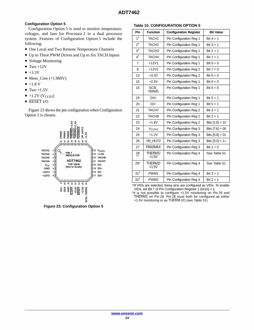
Configuration Option 5Configuration Option 5 is used to monitor temperature,
voltages, and fans for Processor 2 in a dual processorsystem. Features of Configuration Option 5 include thefollowing:• One Local and Two Remote Temperature Channels• Up to Three PWM Drives and Up to Six TACH Inputs• Voltage Monitoring• Two +12V• +3.3V• Mem_Core (+1.969V)• +1.8 V• Two +1.5V• +1.2V (VCCP2)• RESET I/O
Figure 23 shows the pin configuration when ConfigurationOption 5 is chosen.
Figure 23. Configuration Option 5
TH
ER
M2/
+1.5
VT
HE
RM
1/+1
.5V
1TACH12TACH23TACH34TACH4
+12V18+12V2
24 VCCP223 +1.8V22 TACH821 TACH720 D3–19 D3+
9 10 11 12 13+3
.3V
14 15+2
.5V
16S
CS
I_T
ER
M1
32P
WM
231
PW
M1
30 29 28 27FA
N2M
AX
26V
R_H
OT
225
+1.2
V
ADT7462TOP VIEW
(Not to Scale)VCC
GND
SC
LS
DA
AD
DA
LE
RT
RE
SE
T
PW
M3
PIN 1INDICATOR
5
6
7 18
17
D2−D2+
Table 10. CONFIGURATION OPTION 5
Pin Function Configuration Register Bit Value
1† TACH1 Pin Configuration Reg 1 Bit 4 = 1
2† TACH2 Pin Configuration Reg 1 Bit 3 = 1
3† TACH3 Pin Configuration Reg 1 Bit 2 = 1
4† TACH4 Pin Configuration Reg 1 Bit 1 = 1
7 +12V1 Pin Configuration Reg 1 Bit 0 = 0
8 +12V2 Pin Configuration Reg 2 Bit 7 = 0
13 +3.3V Pin Configuration Reg 2 Bit 6 = 0
15 +2.5V Pin Configuration Reg 1 Bit 6 = 0
16 SCSI_TERM1
Pin Configuration Reg 1 Bit 6 = 0
19 D3+ Pin Configuration Reg 1 Bit 5 = 1
20 D3− Pin Configuration Reg 1 Bit 5 = 1
21 TACH7 Pin Configuration Reg 2 Bit 3 = 1
22 TACH8 Pin Configuration Reg 2 Bit 2 = 1
23 +1.8V Pin Configuration Reg 2 Bits [1:0] = 10
24 VCCP2 Pin Configuration Reg 3 Bits [7:6] = 00
25 +1.2V Pin Configuration Reg 3 Bits [5:4] = 01
26 VR_HOT2 Pin Configuration Reg 3 Bits [3:2] = 1×
27 FAN2MAX Pin Configuration Reg 3 Bit 1 = 0
28†*
THERM1/+1.5V
Pin Configuration Reg 4 See Table 51
29* THERM2/+1.5V
Pin Configuration Reg 4 See Table 51
31† PWM1 Pin Configuration Reg 4 Bit 3 = 1
32† PWM2 Pin Configuration Reg 4 Bit 2 = 1
†If VIDs are selected, these pins are configured as VIDs. To enableVIDs, set Bit 7 of Pin Configuration Register 1 (0x10) = 1.
*It is not possible to configure +1.5V monitoring on Pin 29 andTHERM1 on Pin 28. Pin 28 must both be configured as either+1.5V monitoring or as THERM I/O (see Table 51).
ADT7462
www.onsemi.com15
Serial Bus InterfaceThe ADT7462 is controlled through use of the serial
system management bus (SMBus). The ADT7462 isconnected to this bus as a slave device, under the control ofa master controller. The SMBus interface in the ADT7462is fully SMBus 1.1 and SMBus 1.0 compliant. The SMBusaddress is determined by the state of the ADD input onpowerup.
ADD InputThe ADD pin is a three-state input to the ADT7462. It is
used to determine the SMBus address used. This pin issampled on powerup only. Any changes subsequent topowerup are not reflected until the ADT7462 is powereddown and back up again. The corresponding 7-bit SMBusaddress for the state of the ADD pin is shown in Table 11.
Table 11. CORRESPONDING SMBUS ADDRESSESFOR ADD INPUT
ADD Pin SMBus Version SMBus Address
High N/A N/A
Float SMBus 1.1 0x5C
Low SMBus 1.1 0x58
SMBus Fixed AddressThe ADT7462 supports SMBus fixed address mode and
is fully backward compatible with SMBus 1.1 and SMBus1.0. The ADT7462 powers up with a fixed SMBus addressthat cannot be changed by the assign address call. The fixedaddress is set by the state of the ADD input pin on powerup.The ADT7462 also responds to the SMBus device defaultaddress of 0x61.
SMBus OperationThe SMBus specification defines specific conditions for
different types of read and write operations. The generalSMBus protocol operates as follows:
1. The master initiates data transfer by establishing astart condition, defined as a high-to-low transitionon the serial data line, SDA, while the serial clockline, SCL, remains high. This indicates that anaddress/data stream follows. All slave peripheralsconnected to the serial bus respond to the startcondition and shift in the next eight bits, consistingof a 7-bit address (MSB first) plus a R/W bit,which determines the direction of the data transfer,that is, whether data is written to or read from theslave device.
2. The peripheral whose address corresponds to thetransmitted address responds by pulling the dataline low during the low period before the 9th clockpulse, known as the acknowledge bit. All otherdevices on the bus remain idle while the selecteddevice waits for data to be read from it or writtento it. If the R/W bit = 0, the master writes to theslave device. If the R/W bit = 1, the master readsfrom the slave device.
3. Data is sent over the serial bus in sequences ofnine clock pulses: eight bits of data followed by anacknowledge bit from the slave device. Transitionson the data line must occur during the low periodof the clock signal and remain stable during thehigh period, because a low-to-high transition whenthe clock is high can be interpreted as a stopsignal. The number of data bytes that can betransmitted over the serial bus in a single read orwrite operation is limited only by what the masterand slave devices can handle.
4. When all data bytes have been read or written,stop conditions are established. In write mode, themaster releases the data line during the 10th clockpulse to assert a stop condition. In read mode, themaster device overrides the acknowledge bit bypulling the data line high during the low periodbefore the 9th clock pulse. This is known as a noacknowledge. The master then takes the data linelow during the low period before the 10th clockpulse and then takes it high during the 10th clockpulse to assert a stop condition.
Any number of bytes of data can be transferred over theserial bus in one operation, but it is not possible to mix readand write in one operation because the type of operation isdetermined at the beginning and cannot subsequently bechanged without starting a new operation.
For the ADT7462, write operations contain either one ortwo bytes, and read operations contain one byte. To writedata to one of the device data registers or to read data fromit, the address pointer register must be set so that the correctdata register is addressed. Then data can be written into thatregister or read from it. The first byte of a write operationalways contains an address that is stored in the addresspointer register. If data is to be written to the device, the writeoperation contains a second data byte that is written to theregister selected by the address pointer register.
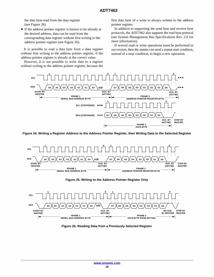
This write operation is shown in Figure 24. The deviceaddress is sent over the bus, and then R/W is set to 0. Thisis followed by two data bytes. The first data byte is theaddress of the internal data register to be written to, whichis stored in the address pointer register. The second data byteis the data to be written to the internal data register.
When reading data from a register, there are twopossibilities.• If the ADT7462 address pointer register value is
unknown or not the desired value, it must be set to thecorrect value before data can be read from the desireddata register. This is done by performing a write to theADT7462 as before, but only the data byte containingthe register address is sent because no data is written tothe register (see Figure 25).A read operation is then performed, consisting of theserial bus address and the R/W bit set to 1, followed by
ADT7462
www.onsemi.com16
the data byte read from the data register(see Figure 26).
• If the address pointer register is known to be already atthe desired address, data can be read from thecorresponding data register without first writing to theaddress pointer register (see Figure 26).
It is possible to read a data byte from a data registerwithout first writing to the address pointer register, if theaddress pointer register is already at the correct value.
However, it is not possible to write data to a registerwithout writing to the address pointer register, because the
first data byte of a write is always written to the addresspointer register.
In addition to supporting the send byte and receive byteprotocols, the ADT7462 also supports the read byte protocol(see System Management Bus Specifications Rev. 2.0 formore information).
If several read or write operations must be performed insuccession, then the master can send a repeat start condition,instead of a stop condition, to begin a new operation.
Figure 24. Writing a Register Address to the Address Pointer Register, then Writing Data to the Selected Register
R/W
SCL
SDA A2 A1 A0 D7 D6 D5 D4 D3 D2 D1 D0
ACK. BYADT7462
START BYMASTER
1 9 1
ACK. BYADT7462
9
D7 D6 D5 D4 D3 D2 D1 D0
ACK. BYADT7462
STOP BYMASTER
1 9
SCL (CONTINUED)
SDA (CONTINUED)
FRAME 1SERIAL BUS ADDRESS BYTE
FRAME 2ADDRESS POINTER REGISTER BYTE
FRAME 3DATA BYTE
A3A4A5A6
Figure 25. Writing to the Address Pointer Register Only
SCL
SDA A2 A1 A0 D7 D6 D5 D4 D3 D2 D1 D0
ACK. BYADT7462
START BYMASTER
1 9 1
ACK. BYADT7462
9
STOP BYMASTER
FRAME 1SERIAL BUS ADDRESS BYTE
FRAME 2ADDRESS POINTER REGISTER BYTE
R/WA3A4A5A6
Figure 26. Reading Data from a Previously Selected Register
SCL
SDA D7 D6 D5 D4 D3 D2 D1 D0
NO ACK.BY MASTER
START BYMASTER
9 1
ACK. BYADT7462
9
STOP BYMASTER
A2 A1 A0
1
FRAME 1SERIAL BUS ADDRESS BYTE
FRAME 2DATA BYTE FROM ADT7462
R/WA3A4A5A6

ADT7462
www.onsemi.com17
Write OperationsThe SMBus specification defines several protocols for
different types of read and write operations. The ones usedin the ADT7462 are discussed below. The followingabbreviations are used in the diagrams:• S − Start• P − Stop• R − Read• W − Write• A − Acknowledge• A − No Acknowledge
The ADT7462 uses the following SMBus write protocols.
Send ByteIn this operation, the master device sends a single
command byte to a slave device as follows:1. The master device asserts a start condition on SDA.2. The master sends the 7-bit slave address followed
by the write bit (low).3. The addressed slave device asserts an ACK on SDA.4. The master sends a command code.5. The slave asserts an ACK on SDA.6. The master asserts a stop condition on SDA to end
the transaction.
For the ADT7462, the send byte protocol is used to writea register address to RAM for a subsequent single byte readfrom the same address. This operation is shown in Figure 27.
Figure 27. Setting a Register Address forSubsequent Read
SLAVEADDRESS
W AS A PREGISTERADDRESS
2 31 5 64
If it is required to read data from the register immediatelyafter setting up the address, the master can assert a repeatstart condition immediately after the final ACK and carryout a single byte read without asserting an intermediate stopcondition.
Write ByteIn this operation, the master device sends a command byte
and one data byte to the slave device as follows:
1. The master device asserts a start condition on SDA.2. The master sends the 7-bit slave address followed
by the write bit (low).3. The addressed slave device asserts an ACK on SDA.4. The master sends a command code.5. The slave asserts an ACK on SDA.6. The master sends a data byte.7. The slave asserts an ACK on SDA.8. The master asserts a stop condition on SDA to end
the transaction.
Figure 28. Single-byte Write to a Register
SLAVEADDRESS W A DATAS A A PSLAVE
ADDRESS
2 31 5 6 7 84
Block WriteIn this operation, the master device writes a block of data
to a slave device. The start address for a block write must beset previously. In the case of the ADT7462, this is done bya send byte operation to set a RAM address. The user writesthe number of registers to be written to in the block readcommand to the #Bytes bits of the Configuration 0 register.
1. The master device asserts a start condition on SDA.2. The master sends the 7-bit slave address followed
by the write bit (low).3. The addressed slave device asserts an ACK on SDA.4. The master sends a command code that tells the
slave device to expect a block write. TheADT7462 command code for a block write is0xA0 (1010 0000).
5. The slave asserts an ACK on SDA.6. The master sends the data bytes (the number of
data bytes sent is written to the #Bytes bits of theConfiguration 0 register).
7. The slave asserts an ACK on SDA after each databyte.
8. The master sends a packet error checking (PEC) byte.9. The ADT7462 checks the PEC byte and issues an
ACK, if correct. If incorrect (NO ACK), themaster resends the data bytes.
10. The master asserts a stop condition on SDA to endthe transaction.
Figure 29. Block Write to ADT7462
S W A A A DATA 1 A A A PDATA 2 ADATA
32PEC
SLAVEADDRESS
COMMAND0xA0
BLOCKWRITE
BYTECOUNT
1 2 3 4 5 6 7 8 9 10 11 12

ADT7462
www.onsemi.com18
Read OperationsThe ADT7462 uses the following SMBus read protocols.
Receive ByteThe receive byte is useful when repeatedly reading a
single register. The register address must be set uppreviously. In this operation, the master device receives asingle byte from a slave device as follows:
1. The master device asserts a start condition on SDA.2. The master sends the 7-bit slave address followed
by the read bit (high).3. The addressed slave device asserts an ACK on SDA.4. The master receives a data byte.5. The master asserts a NO ACK on SDA.6. The master asserts a stop condition on SDA to end
the transaction.
For the ADT7462, the receive byte protocol is used to reada single byte of data from a register whose address haspreviously been set by a send byte or write a byte operation.
Figure 30. Single-byte Read from a Register
SLAVEADDRESS DATAARS A P
2 431 5 6
Block ReadIn this operation, the master device reads a block of data
from a slave device. The start address for a block read mustbe set previously, as well as the number of bytes to be read(maximum = 32). In the case of the ADT7462, the startaddress is activated by a send byte operation to set a RAMaddress. The number of bytes to be read should be written tothe #Bytes bits in the Configuration 0 register. The blockread operation consists of a send byte operation that sendsa block read command to the slave, immediately followed bya repeated start and a read operation that reads out multipledata bytes, as follows:
1. The master device asserts a start condition on SDA.2. The master sends the 7-bit slave address followed
by the write bit (low).3. The addressed slave device asserts an ACK on SDA.4. The master sends a command code that tells the slave
device to expect a block read. The ADT7462command code for a block read is 0xA1 (1010 0001).
5. The slave asserts an ACK on SDA.6. The master asserts a repeat start condition on SDA.7. The master sends the 7-bit slave address followed
by the read bit (high).8. The slave asserts an ACK on SDA.9. The ADT7462 sends a byte count telling the
master how many data bytes to expect. Themaximum number of bytes is 32.
10. The master asserts an ACK on SDA.11. The master receives the expected number of data
bytes.
12. The master asserts an ACK on SDA after eachdata byte.
13. The ADT7462 issues a PEC byte to the master.The master should check the PEC byte and issueanother block read if the PEC byte is incorrect.
14. A NO ACK is generated after the PEC byte tosignal the end of the read.
15. The master asserts a stop condition on SDA to endthe transaction.
Figure 31. Block Read from RAM
S SLAVEADDRESS W A
COMMAND0xA1 BLOCK
READA S R
A PDATA32 PECA BYTE
COUNT A DATA 1 A
SLAVEADDRESS
A
1
8 9 10 12 13 14 1511
2 3 4 5 6 7
Note that although the ADT7462 supports packet errorchecking (PEC), its use is optional. The PEC byte iscalculated using CRC−8. The frame check sequence (FCS)conforms to CRC−8 by the polynomial.
C(x) � x8 � x2 � x � 1
Consult the SMBus 1.1 specifications for more information.
Alert Response AddressAlert Response Address (ARA) is a feature of SMBus
devices that allows an interrupting device to identify itselfto the host when multiple devices exist on the same bus.
The SMBALERT output can be used as either an interruptoutput or an SMBALERT. One or more outputs can beconnected to a common SMBALERT line connected to themaster. If a device’s SMBALERT line goes low, thefollowing procedure occurs:
1. SMBALERT is pulled low.2. The master initiates a read operation and sends the
alert response address (ARA = 0001 100). This isa general call address that must not be used as aspecific device address.
3. The device whose SMBALERT output is lowresponds to the ARA, and the master reads itsdevice address. The address of the device is nowknown and can be interrogated in the usual way.
4. If more than one device’s SMBALERT output islow, the one with the lowest device address haspriority in accordance with normal SMBusarbitration.
5. Once the ADT7462 has responded to the ARA, themaster must read the status registers, and theSMBALERT is cleared only if the error conditionhas gone away.

ADT7462
www.onsemi.com19
SMBus TimeoutThe ADT7462 includes an SMBus timeout feature. If
there is no SMBus activity for 25 ms, the ADT7462 assumesthat the bus is locked and releases the bus. This prevents thedevice from locking or holding the SMBus while the deviceis expecting data. Some SMBus controllers cannot handlethe SMBus timeout feature, so it can be disabled.
Configuration Register 3 (0x03)
Bit 1 SCL_Timeout = 1; SCL Timeout Enabled
Bit 1 SCL_Timeout = 0; SCL Timeout Disabled (Default)
Bit 2 SDA_Timeout = 1; SDA Timeout Enabled
Bit 2 SDA_Timeout = 0; SDA Timeout Disabled (Default)
Temperature and Voltage Measurement
Temperature MeasurementThe ADT7462 can measure its own ambient temperature
and the temperature of up to three remote thermal diodes.These diodes can be discrete diode-connected 2N3904/2N3906s or they can be located on a processor die. Figure 32shows how to connect a remote NPN or PNP transistor.
Figure 32. How to Measure Temperature UsingDiscrete Transistors
ADT7462 ADT7462
D+
D−
D+
D−
2N3904
2N3906
Remote Thermal Diode 1 connects to Pin 15 and Pin 16.
Remote Thermal Diode 2 connects to Pin 17 and Pin 18.
Remote Thermal Diode 3 connects to Pin 19 and Pin 20.
A simple method of measuring temperature is to exploitthe negative temperature coefficient of a diode, measuringthe base-emitter voltage (VBE) of a transistor, operated atconstant current. Unfortunately, this technique requirescalibration to cancel the effect of the absolute value of VBE,which varies from device to device.
The technique used in the ADT7462 is to measure thechange in VBE when the device is operated at three differentcurrents. Previous devices have used only two operatingcurrents; use of a third current allows automatic cancellationof any resistances in series with the external temperaturesensor.
Figure 33 shows the input signal conditioning used tomeasure the output of an external temperature sensor. This
figure shows the external sensor as a substrate transistor, butit could equally be a discrete transistor. If a discretetransistor is used, the collector is not grounded and shouldbe linked to the base. To prevent ground noise frominterfering with the measurement, the more negativeterminal of the sensor is not referenced to ground but isbiased above ground by an internal diode at the D− input. C1can optionally be added as a noise filter (recommendedmaximum value 1000 pF). However, a better option in noisyenvironments is to add a filter, as described in the NoiseFiltering section.
To measure �VBE, the operating current through thesensor is switched among three related currents. As shownin Figure 33, N1 × I and N2 × I are different multiples of theCurrent I. The currents through the temperature diode areswitched between I and N1 × I, giving �VBE1, and thenbetween I and N2 × I, giving �VBE2. The temperature canthen be calculated using the two �VBE measurements. Thismethod can also be shown to cancel the effect of any seriesresistance on the temperature measurement.
The resulting �VBE waveforms are passed through a65 kHz low-pass filter to remove noise and then to achopper-stabilized amplifier. This amplifies and rectifies thewaveform to produce a dc voltage proportional to �VBE.The ADC digitizes this voltage, and a temperaturemeasurement is produced. To reduce the effects of noise,digital filtering is performed by averaging the results of 16measurement cycles for low conversion rates.
Signal conditioning and measurement of the internaltemperature sensor are performed in the same manner (seeFigure 33).
Temperature Measurement ResultsThe results of the local and remote temperature
measurements are stored in the local and remote temperaturevalue registers and are compared with limits programmedinto the local and remote high and low limit registers.
Table 12. TEMPERATURE MEASUREMENTREGISTERS
Temperature Value Register Address
Local Temperature, LSB Register 0x88, Bits [7:6]
Local Temperature, MSB Register 0x89
Remote 1 Temperature, LSB Register 0x8A, Bits [7:6]
Remote 1 Temperature, MSB Register 0x8B
Remote 2 Temperature, LSB Register 0x8C, Bits [7:6]
Remote 2 Temperature, MSB Register 0x8D
Remote 3 Temperature, LSB Register 0x8E, Bits [7:6]
Remote 3 Temperature, MSB Register 0x8F

ADT7462
www.onsemi.com20
Figure 33. Input Signal Conditioning
LOW-PASS FILTERfC = 65 kHz
REMOTESENSING
TRANSISTOR
BIASDIODE
D+
D−
VCCIBIASI N1 × I
VOUT+
VOUT−
To ADC
N2 × I
C1*
*CAPACITOR C1 IS OPTIONAL. IT SHOULD ONLY BE USED IN NOISY ENVIRONMENTS.
The temperature value is stored in two registers. The MSBhas a resolution of 1°C. Only two bits in the temperatureLSB register are used, Bit 7 and Bit 6, giving a temperaturemeasurement resolution of 0.25°C. The temperaturemeasurement range for both local and remote measurementsis from −64°C to +191°C. However, the ADT7462 itselfshould never be operated outside its operating temperaturerange, which is from −40°C to +125°C. For the remotediode, the user should refer to the data sheet of the diode.
Table 13. TEMPERATURE DATA FORMAT
Temperature Value MSB LSB
−64°C 0000 0000 0000 0000
−50.25°C 0000 1110 0100 0000
−25°C 0010 0111 0000 0000
0°C 0100 0000 0000 0000
+25°C 0101 1001 0000 0000
+50.25°C 0111 0010 0100 0000
+100°C 1010 0100 0000 0000
When reading the full temperature value, the LSB shouldbe read first and then the MSB. Reading the LSBs causes thecurrent MSBs to be frozen until they are read. Reading theMSBs only does not cause any register to be locked. This isuseful when a temperature reading with 1°C resolution isrequired.
Series Resistance CancellationParasitic resistance in series with the remote diode D+ and
D− inputs can be caused by a variety of factors, includingPCB track resistance and track length. This series resistance
appears as a temperature offset in the remote sensor’stemperature measurement. This error typically causes a0.8°C offset per ohm of parasitic resistance in series with theremote diode.
The ADT7462 automatically cancels out the effect of thisseries resistance on the temperature reading, giving a moreaccurate result, without the need for user characterization ofthis resistance. The ADT7462 is designed to automaticallycancel typically up to 2 k� of resistance. By using anadvanced temperature measurement method, the process istransparent to the user. This feature also allows an RCR filterto be added to the sensor path, allowing the part to be usedaccurately in noisy environments.
Temperature LimitsEach temperature measurement channel has a high and
low temperature limit associated with it. The temperaturemeasurements are compared with these limits, and theresults of these comparisons are stored in status registers. ALogic 0 indicates an in-limit comparison, and a Logic 1indicates an out-of-limit comparison. The ADT7462 cangenerate an ALERT, if configured to do so, after a status bitis set. For more information on the status registers andALERT, see the Status and Mask Registers ALERT section.
Each temperature channel also has a THERM1 and aTHERM2 temperature limit associated with it. When thesetemperature limits are exceeded, the correspondingTHERM pin is asserted low (if THERM is configured as anoutput), and the fans are boosted to full speed (if the boostbit is set). Table 14 shows a complete list of all thetemperature limits and their default values.
ADT7462
www.onsemi.com21
Table 14. TEMPERATURE LIMIT REGISTERS
Temperature ValueRegisterAddress Default
Local Low Temperature Limit 0x44 0x40
Remote 1 Low Temperature Limit 0x45 0x40
Remote 2 Low Temperature Limit 0x46 0x40
Remote 3 Low Temperature Limit 0x47 0x40
Local High Temperature Limit 0x48 0x95
Remote 1 High Temperature Limit 0x49 0x95
Remote 2 High Temperature Limit 0x4A 0x95
Remote 3 High Temperature Limit 0x4B 0x95
Local THERM1 Temperature Limit 0x4C 0xA4
Remote 1 THERM1 Temperature Limit 0x4D 0xA4
Remote 2 THERM1 Temperature Limit 0x4E 0xA4
Remote 3 THERM1 Temperature Limit 0x4F 0xA4
Local THERM2 Temperature Limit 0x50 0xA4
Remote 1 THERM2 Temperature Limit 0x51 0xA4
Remote 2 THERM2 Temperature Limit 0x52 0xA4
Remote 3 THERM2 Temperature Limit 0x53 0xA4
Offset RegistersThe ADT7462 has temperature offset registers at Register
0x56 to Register 0x59 for the local, Remote 1, Remote 2, andRemote 3 temperature channels. By doing a one-timecalibration of the system, the user can determine the offsetcaused by system board noise and cancel it using the offsetregisters. The offset registers automatically add a twoscomplement, 8-bit reading to every temperaturemeasurement. The LSBs add 0.5°C offset to the temperaturereading so the 8-bit register effectively allows temperatureoffsets of up to ±64°C with a resolution of 0.5°C. This ensuresthat the readings in the temperature measurement registers areas accurate as possible.
Temperature Offset Registers
Register 0x56 Local Temperature Offset = 0x00(0°C Default)
Register 0x57 Remote 1 Temperature Offset = 0x00(0°C Default)
Register 0x58 Remote 2 Temperature Offset = 0x00(0°C Default)
Register 0x59 Remote 3 Temperature Offset = 0x00(0°C Default)
Layout ConsiderationsDigital boards can be electrically noisy environments.
The ADT7462 measures very small voltages from theremote sensor, so care must be taken to minimize noiseinduced at the sensor inputs. The following precautionsshould be taken:
• Place the ADT7462 as close as possible to the remotesensing diode. Provided that the worst noise sources,such as clock generators, data/address buses, and CRTs,are avoided, this distance can be 4 inches to 8 inches.
• Route the D+ and D− tracks close together, in parallel,with grounded guard tracks on each side. To minimizeinductance and reduce noise pickup, a 5 mil track widthand spacing is recommended. If possible, provide aground plane under the tracks.
Figure 34. Typical Arrangement of Signal Tracks
5 MIL
5 MIL
5 MIL
5 MIL
5 MIL
5 MIL
5 MIL
GND
D−
D+
GND
• Minimize the number of copper/solder joints that cancause thermo-couple effects. Where copper/solderjoints are used, make sure that they are in both the D+and D− path and at the same temperature.
• Thermocouple effects should not be a major problembecause 1°C corresponds to about 200 mV, andthermocouple voltages are about 3 mV/°C oftemperature difference. Unless there are twothermocouples with a large temperature differentialbetween them, thermocouple voltages should be muchless than 200 mV.
• Place a 0.1 �F bypass capacitor close to the VCC pin. Inextremely noisy environments, an input filter capacitorcan be placed across D+ and D− close to the ADT7462.This capacitance can affect the temperaturemeasurement, so care must be taken to ensure that anycapacitance seen at D+ and D− is a maximum of1000 pF. This maximum value includes the filtercapacitance, plus any cable or stray capacitancebetween the pins and the sensor diode.
• If the distance to the remote sensor is more than8 inches, the use of twisted pair cable is recommended.This works from about 6 feet up to 12 feet.
• For really long distances (up to 100 feet), use shieldedtwisted pair, such as Belden No. 8451 microphonecable. Connect the twisted pair to D+ and D− and theshield to GND close to the ADT7462. Leave the remoteend of the shield unconnected to avoid ground loops.
• Because the measurement technique uses switchedcurrent sources, excessive cable or filter capacitancecan affect the measurement. When using long cables,the filter capacitance can be reduced or removed.
ADT7462
www.onsemi.com22
Noise FilteringFor temperature sensors operating in noisy environments,
the industry-standard practice is to place a capacitor acrossthe D+ and D− pins to help combat the effects of noise.However, large capacitances affect the accuracy of thetemperature measurement, leading to a recommendedmaximum capacitor value of 1000 pF. While this capacitordoes reduce noise, it does not eliminate it, making it difficultto use the sensor in a very noisy environment.
The ADT7462 has a major advantage over other devicesin eliminating the effects of noise on the external sensor. Theseries resistance cancellation feature allows a filter to beconstructed between the external temperature sensor and thedevice. The effect of any filter resistance seen in series withthe remote sensor is automatically canceled from thetemperature result.
The construction of a filter allows the ADT7462 and theremote temperature sensor to operate in noisy environments.Figure 35 shows a low-pass RCR filter, with the followingvalues:
R = 100 �C = 1 nF
This filtering reduces both common-mode noise anddifferential noise.
Figure 35. Filter Between Remote Sensor andADT7462
100 �
100 �1 nF
D+
D−
REMOTESENSOR
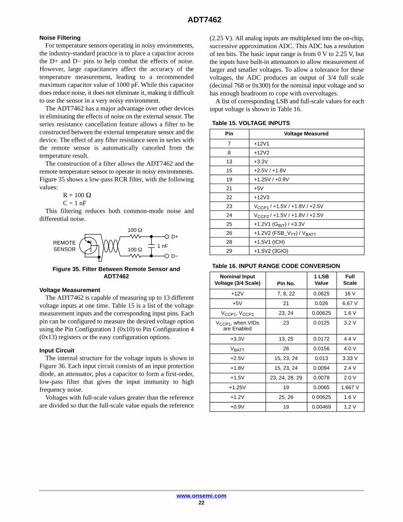
Voltage MeasurementThe ADT7462 is capable of measuring up to 13 different
voltage inputs at one time. Table 15 is a list of the voltagemeasurement inputs and the corresponding input pins. Eachpin can be configured to measure the desired voltage optionusing the Pin Configuration 1 (0x10) to Pin Configuration 4(0x13) registers or the easy configuration options.
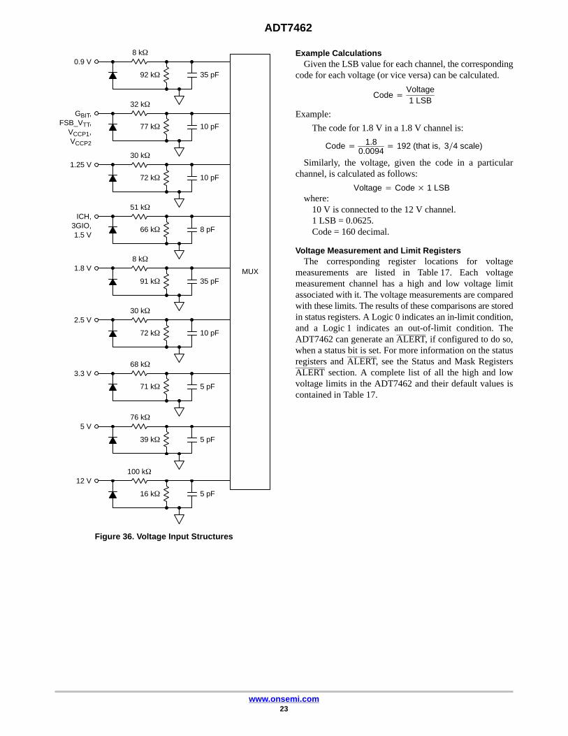
Input CircuitThe internal structure for the voltage inputs is shown in
Figure 36. Each input circuit consists of an input protectiondiode, an attenuator, plus a capacitor to form a first-order,low-pass filter that gives the input immunity to highfrequency noise.
Voltages with full-scale values greater than the referenceare divided so that the full-scale value equals the reference
(2.25 V). All analog inputs are multiplexed into the on-chip,successive approximation ADC. This ADC has a resolutionof ten bits. The basic input range is from 0 V to 2.25 V, butthe inputs have built-in attenuators to allow measurement oflarger and smaller voltages. To allow a tolerance for thesevoltages, the ADC produces an output of 3/4 full scale(decimal 768 or 0x300) for the nominal input voltage and sohas enough headroom to cope with overvoltages.
A list of corresponding LSB and full-scale values for eachinput voltage is shown in Table 16.
Table 15. VOLTAGE INPUTS
Pin Voltage Measured
7 +12V1
8 +12V2
13 +3.3V
15 +2.5V / +1.8V
19 +1.25V / +0.9V
21 +5V
22 +12V3
23 VCCP1 / +1.5V / +1.8V / +2.5V
24 VCCP2 / +1.5V / +1.8V / +2.5V
25 +1.2V1 (GBIT) / +3.3V
26 +1.2V2 (FSB_VTT) / VBATT
28 +1.5V1 (ICH)
29 +1.5V2 (3GIO)
Table 16. INPUT RANGE CODE CONVERSION
Nominal InputVoltage (3/4 Scale) Pin No.
1 LSBValue
FullScale
+12V 7, 8, 22 0.0625 16 V
+5V 21 0.026 6.67 V
VCCP1, VCCP2 23, 24 0.00625 1.6 V
VCCP1, when VIDsare Enabled
23 0.0125 3.2 V
+3.3V 13, 25 0.0172 4.4 V
VBATT 26 0.0156 4.0 V
+2.5V 15, 23, 24 0.013 3.33 V
+1.8V 15, 23, 24 0.0094 2.4 V
+1.5V 23, 24, 28, 29 0.0078 2.0 V
+1.25V 19 0.0065 1.667 V
+1.2V 25, 26 0.00625 1.6 V
+0.9V 19 0.00469 1.2 V
ADT7462
www.onsemi.com23
Figure 36. Voltage Input Structures
8 k�
35 pF
0.9 V
92 k�
32 k�
10 pF
GBIT,FSB_VTT,
VCCP1,VCCP2
77 k�
30 k�
10 pF
1.25 V
72 k�
51 k�
8 pF
ICH,3GIO,1.5 V
66 k�
8 k�
35 pF
1.8 V
91 k�
30 k�
10 pF
2.5 V
72 k�
68 k�
5 pF
3.3 V
71 k�
76 k�
5 pF
5 V
39 k�
100 k�
5 pF
12 V
16 k�
MUX
Example CalculationsGiven the LSB value for each channel, the corresponding
code for each voltage (or vice versa) can be calculated.
Code �Voltage1 LSB
Example:
The code for 1.8 V in a 1.8 V channel is:
Code � 1.80.0094
� 192 (that is, 3�4 scale)
Similarly, the voltage, given the code in a particularchannel, is calculated as follows:
Voltage � Code � 1 LSBwhere:
10 V is connected to the 12 V channel.1 LSB = 0.0625.Code = 160 decimal.
Voltage Measurement and Limit RegistersThe corresponding register locations for voltage
measurements are listed in Table 17. Each voltagemeasurement channel has a high and low voltage limitassociated with it. The voltage measurements are comparedwith these limits. The results of these comparisons are storedin status registers. A Logic 0 indicates an in-limit condition,and a Logic 1 indicates an out-of-limit condition. TheADT7462 can generate an ALERT, if configured to do so,when a status bit is set. For more information on the statusregisters and ALERT, see the Status and Mask RegistersALERT section. A complete list of all the high and lowvoltage limits in the ADT7462 and their default values iscontained in Table 17.

ADT7462
www.onsemi.com24
Table 17. VOLTAGE VALUE AND LIMIT REGISTERS
Voltage Value Pin No. Value Register Address
Low Limit High Limit
Register Default Register Default
+12V1 7 0xA3 0x6D 0x00 0x7C 0xFF
+12V2 8 0xA5 0x6E 0x00 0x7D 0xFF
+3.3V 13 0x96 0x70 0x00 0x68 0xFF
+1.8V or +2.5V 15 0x8B 0x45 0x40 0x49 0x95
+1.25V or +0.9V 19 0x8F 0x47 0x40 0x4B 0x95
+5V 21 0xA7 0x71 0x00 0x7E 0xFF
+12V3 22 0xA9 0x6F 0x00 0x7F 0xFF
VCCP1, +1.5V, +1.8V, +2.5V 23 0x90 0x72 0x20 0x69 0xFF
VCCP2, +1.5V, +1.8V, +2.5V 24 0x91 0x73 0x00 0x6A 0xFF
+1.2V1 (GBIT) or +3.3V 25 0x92 0x74 0x00 0x6B 0xFF
+1.2V2 (FSB_VTT) or VBATT 26 0x93 0x75 0x80 0x6C 0xFF
+1.5V1 (ICH) 28 0x94 0x77 0x00 0x50 0xA4
+1.5V2 (3GIO) 29 0x95 0x76 0x00 0x4C 0xA4
Battery Measurement Input (VBATT)The VBATT input allows the condition of a CMOS backup
battery to be monitored. This is typically a lithium coin cell,such as a CR2032. The VBATT input is accurate only forvoltages greater than 1.2 V. Note that when Pin 26 isconfigured as a +1.2V input, voltages lower than 1.2 V arenot accurately measured. Input voltage and correspondingvoltage measured are shown in Figure 16.
Typically, the battery in a system is required to keep somedevices powered on when the system is in a powered-offstate. The VBATT measurement input is designed to minimizebattery drain. To reduce current drain from the battery, thelower resistor of the VBATT attenuator is not connected,except when a VBATT measurement is being made. The totalcurrent drain on the VBATT pin is 80 nA typical (for amaximum VBATT voltage = 4.0 V), so a CR2032 CMOSbattery functions in a system in excess of the expected10 years. Note that when a VBATT measurement is not beingmade, the current drain is reduced to 16 nA typical. Undernormal voltage measurement operating conditions, allmeasurements are made in a round-robin format, and eachreading is actually the result of 16 digitally averagedmeasurements. However, averaging is not carried out on theVBATT measurement to reduce measurement time and,therefore, reduce the current drain from the battery.
The VBATT current drain when a measurement is beingmade is calculated by:
I �VBATT100 k�
�tpulse
tperiod
where:
tPULSE is the VBATT measurement time (~711 �s typical). tPERIOD is the time required to measure all analog inputs.
Monitoring cycle time depends on the ADT7462configuration. Calculating the monitoring cycle time isdescribed in more detail in the ADC Information section.
VBATT Input Battery ProtectionIn addition to minimizing battery current drain, the VBATT
measurement circuitry is specifically designed with batteryprotection in mind. Internal circuitry prevents the batteryfrom being back-biased by the ADT7462 supply or throughany other path under normal operating conditions. In theunlikely event of a catastrophic ADT7462 failure, theADT7462 includes a second level of battery protection,including a series 3 k� resistor to limit current to the battery,as recommended by UL (see Figure 37). Thus, it is notnecessary to add a series resistor between the battery and theVBATT input; the battery can be connected directly to theVBATT input to improve voltage measurement accuracy.
Figure 37. Equivalent VBATT Input Protection Circuit
ADC
DIGITALCONTROL
VBATT
49.5 k�
82.7 k�3 k�
3 k�
4.5 pF

ADT7462
www.onsemi.com25
ADC Information
Round RobinBoth temperature and voltage measurements are analog
inputs that are digitized using the on-board ADC. Aninternal multiplexer switches between the different analoginputs and digitizes them, in turn, in a round-robin manner.The total conversion time depends upon how the ADT7462is configured. The conversion times for each measurementchannel are shown in Table 18. The complete conversiontime is the sum of the time for the voltage and temperaturemeasurements.
For example, if the ADT7462 is configured as EasyConfiguration Option 1, the round-robin conversion time iscalculated as follows:
Total Conversion Time =1 × (Local Conversion Time) +3 × (Remote Conversion Time) +4 × (Voltage Measurement Time)
The TACH is not measured using the ADC and so is notpart of the round-robin monitoring cycle.
Table 18. MEASUREMENT CHANNEL CONVERSIONTIMES
Channel Conversion Time (ms)
Local Temperature 9.01
Remote Temperature 38.36
Voltage 8.53
For each ADC temperature and voltage measurement readfrom their value registers, 16 readings have actually beenmade internally and the results averaged before being placedin the value register.
Bypass Voltage AttenuatorsThere are up to 13 voltage measurement channels on the
ADT7462. Each of these voltage measurement channels hasan input structure (see Figure 36 for input structures for eachof the voltage channels). Because the ADC has a voltageinput range from 0 V to 2.25 V, these input circuits attenuatethe voltage input using a resistor divider network to matchthe input range of the ADC. However, the user mayoccasionally want to remove the attenuators and directlyapply a voltage of between 0 V and 2.25 V to the ADC.These attenuators can be disabled by setting relevant bits inthe voltage attenuator configuration registers (see Table 19).This feature also allows the user to rescale the voltage inputsusing an external attenuator circuit. However, when theattenuators are disabled, the user should ensure that thevoltage on the pin never exceeds 2.25 V.
Table 19. VOLTAGE ATTENUATOR CONFIGURATIONREGISTERS
Register Name Register Address
Voltage AttenuatorConfiguration Register 1
0x18
Voltage AttenuatorConfiguration Register 2
0x19
Single-channel ADC ConversionsSetting Bit 2 of the EDO Enable register (0x16) places the
ADT7462 into single-channel mode. In this mode, theADT7462 can be made to convert on a single voltage ortemperature channel only. The channel to be converted on isselected by writing to Bits [7:3] of the EDO (single-channel)Enable register (0x16). When the device is in single-channelmode, the pin configuration option should not be changed.
Note that when the Pin 26 voltage, which includes theVBATT option, is selected in single-channel mode, thismeans that voltage measurements are continuously made inthis mode. If a battery is connected to this input, this resultsin an excessive current drain on the battery. Thespecification of >10 years of battery life is valid only whenthe battery voltage is measured as part of the round robin andnot in single-channel mode.
Table 20. SINGLE-CHANNEL MODE OPTIONS
Bits [7:3] ADC Channel Selected
0000 0 +1.2V2 Voltage, Pin 26
0000 1 Remote 1 Temperature
0001 0 Remote 2 Temperature
0001 1 Remote 3 Temperature
0010 0 Local Temperature
0010 1 +12V1 Voltage, Pin 7
0011 0 +12V2 Voltage, Pin 8
0011 1 +12V3 Voltage, Pin 22
0100 0 +3.3V Voltage, Pin 13
0100 1 +2.5V/+1.8V Voltage, Pin 15
0101 0 +1.25V/+0.9V Voltage, Pin 19
0101 1 +5V Voltage, Pin 21
0110 0 +1.5V/+1.8V/+2.5V Voltage, Pin 23
0110 1 +1.5V/+1.8V/+2.5V Voltage, Pin 24
0111 0 +1.2V1/+3.3V Voltage, Pin 25
1000 0 +1.5V1 Voltage, Pin 28
1000 1 +1.5V2 Voltage, Pin 29

ADT7462
www.onsemi.com26
Dynamic VID Functionality
VID CodeThe ADT7462 can be configured to monitor up to seven
VID inputs. The VID code is output on seven lines from theCPU to tell the power controller what input voltage itrequires. The ADT7462 can monitor the VID code and thevoltage applied to the CPU to ensure that they match withinan acceptable range. This acceptable range is programmablein the ADT7462.
The VID lines are monitored by the ADT7462, and theVID code is stored in the VID Value register (0x97), whichcan be read back over the SMBus.
VID monitoring is enabled by setting Bit 7 (VIDs) of PinConfiguration Register 1 (0x10) to 1. See Table 21 andTable 22 for information on which pin should be connectedto each VID line. When VID monitoring is enabled, all sevenpins are automatically configured as VID inputs. It is notpossible to select six pins as VID inputs and use theremaining pin as an alternate function.
VID Value Register (0x97)
Bit 0 = VID0 (reflects the logic state of Pin 1)
Bit 1 = VID1 (reflects the logic state of Pin 2)
Bit 2 = VID2 (reflects the logic state of Pin 3)
Bit 3 = VID3 (reflects the logic state of Pin 4)
Bit 4 = VID4 (reflects the logic state of Pin 31)
Bit 5 = VID5 (reflects the logic state of Pin 32)
Bit 6 = VID6 (reflects the logic state of Pin 28)
The ADT7462 supports both the VR10 and the VR11specifications. The default option supports the VR10specification. To switch to the VR11 specification, set Bit 6of Configuration Register 0 (0x00) to 1. VR11 is defined aseight bits; the ADT7462 monitors only seven VID lines (seeTable 21).
Table 21. VR11 VID CODES
VID Number Pin No. Voltage
VID6 28 400 mV
VID5 32 200 mV
VID4 31 100 mV
VID3 4 50 mV
VID2 3 25 mV
VID1 2 12.5 mV
VID0 1 6.25 mV
VR10 requires only six VID lines (see Table 22). Pin 28should be connected to ground when monitoring VR10 VIDcodes. VID6 reports a 0.
Table 22. VR10 VID CODES
VID Number Pin No. Voltage
VID6 28 Unused, Connect to GND
VID5 32 12.5 mV
VID4 31 400 mV
VID3 4 200 mV
VID2 3 100 mV
VID1 2 60 mV
VID0 1 25 mV
Dynamic VID MonitoringThe ADT7462 supports dynamic VID monitoring. The
purpose of the VID code is to tell the voltage controller whatVCCP voltage should be applied to the CPU. The VCCPvoltage applied to the processor changes as the powerrequirements of the processor change. The VID is comparedwith VCCP1 only. Note that when the VIDs are enabled, theLSB value for VCCP1 becomes 0.0125 V (see Table 16).
The VID values can represent voltages from 0.8375 V to1.6 V. The VID code is sampled by the ADT7462 every11 �s and is stored in Register 0x97. Once the VID code hasbeen stable (that is, does not change) for 55 �s, the measuredVCCP is then compared with the VID code. The comparisontable used is for either the VR10 or the VR11 specification(set by Bit 6 of Register 0x00). If the VID code and themeasured VCCP do not match within a certain limit, anALERT is generated.
The VID value decoded and the VCCP measurement mustbe within a window controlled by the VID high and lowlimits. The VID is compared with VCCP1 only. Register 0x78holds the 4-bit VID high and low limits. The high limit hasa range of 0 mV to 375 mV with a resolution of 25 mV (fourbits). The low limit has a range of 0 mV to −187.5 mV witha resolution of 12.5 mV (four bits). The high limit is used ina greater-than comparison, and the low limit is used in aless-than-or-equal-to comparison. Note that if both limitsare set to 0x00, because the low limit is less than or equal tothe comparison, an ALERT always results. Therefore, theminimum value for low limit is 0x01.
If the VCCP voltage measured and the VID code do notmatch to within the programmed limit, Status Bit 6 of thedigital status register is set (Register 0xBE). This, in turn,can generate an ALERT if it is not masked.

ADT7462
www.onsemi.com27
Example
VID high limit: 100 mV (Register 0x78), four MSBs set to0100.
VID low limit: 50 mV (Register 0x78), four LSBs set to 0100.
VID value equates to 1.1 V. This is the read VID decoded,using either VR10 or VR11 tables.
VCCP1 must be in the window of 1.05 V to 1.2 V. If theVCCP1 value is outside this window, the status bit is set andan ALERT is generated.
To clear an ALERT generated in this way, read the digitalstatus register. If the VID code and VCCP are now matchingwithin the programmed window (that is, the error conditionthat caused the ALERT has gone away), then the status bitis reset and so is the ALERT.
The VID to VCCP voltage tables for both VR10 and VR11can be found on the Intel website. See the Voltage RegulatorModule (VRM) and Enterprise Voltage Regulator-Down(EVRD) 10.0 Design Guidelines, Page 18 and Page 19, foradditional information.
Status and Mask Registers and ALERT
Status RegistersEach measured temperature and voltage has an associated
high and low limit. The measured values are compared withthese programmable limits. The results of thesecomparisons are stored in the status registers. A Logic 0 inthe status register represents an in-limit comparison, whilea Logic 1 represents an out-of-limit comparison.
Once a status bit is set, it remains set until the statusregister is read by the SMBus master. Once read, the statusbit is cleared if the error condition has gone away. The statusregisters are duplicated to accommodate situations wherethere are two SMBus masters. If one master reads the hoststatus registers and consequently clears them, the secondmaster has no way of knowing what bits were set and whatbits were cleared. The second SMBus master can read fromthe duplicate BMC status registers to determine which statusbits were set.
Table 23 is a list of the status registers and correspondingaddresses.
Table 23. STATUS REGISTERS
Register NameHost
AddressBMC
Address
Thermal Status Register 1 0xB8 0xC0
Thermal Status Register 2 0xB9 0xC1
Thermal Status Register 3 0xBA −
Voltage Status Register 1 0xBB 0xC3
Voltage Status Register 2 0xBC 0xC4
Fan Status Register 1 0xBD 0xC5
Digital Status Register 1 0xBE 0xC6
GPIO Status Register 0xBF −
ALERT OutputThe ADT7462 has an SMBus ALERT output that is
asserted when one of the status bits is set. This is to alert themaster that an out-of-limit measurement has taken place orthat there is a fault on one of the fan channels.
An ALERT is generated as a result of a status bit being setin any of the registers.
Figure 38. ALERT and Status Bit Behavior
TEMP BACK IN LIMIT(STATUS BIT STAYSSET)
CLEARED ON READ(TEMP BELOW LIMIT)
HIGH LIMIT
TEMPERATURE
STICKYSTATUS BIT
SMBALERT
Figure 38 shows how the ALERT output and “sticky”status bits behave. When a limit is exceeded, thecorresponding status bit is set to 1. The status bit remains setuntil the error condition goes away and the status register isread. The status bits are referred to as sticky because theyremain set until read by software. This ensures that anout-of-limit event cannot be missed, if software is pollingthe device periodically. Note that the ALERT output remainslow for the entire duration that a reading is out of limit anduntil the status register has been read.
Mask RegistersThe user has the option of masking any of the individual
status bits that generate an ALERT. This is achieved bysetting the appropriate bit in the mask registers. The ALERToutput is not asserted on the setting of a status bit if it hasbeen masked. The status bit itself is not affected andcontinues to be set when an out-of-limit condition exists.
Table 24 is a list of the mask registers and correspondingaddresses.
Table 24. MASK REGISTERS
Register Name Register Address
Thermal Mask Register 1 0x30
Thermal Mask Register 2 0x31
Voltage Mask Register 1 0x32
Voltage Mask Register 2 0x33
Fan Mask Register 0x34
Digital Mask Register 0x35
GPIO Mask Register 0x36
Fan Control
Fan Drive Using PWM ControlThe ADT7462 uses pulse-width modulation (PWM) to
control fan speed. Control relies on varying the duty cycle

ADT7462
www.onsemi.com28
(or on/off ratio) of a square wave applied to the fan to varythe fan speed. The advantage of using PWM control is thatit uses a very simple external circuit. The specific circuitused depends upon the type of fan.
There are three main fan types in use: 2-wire fans, 3-wirefans, and 4-wire fans. The 2-wire fan has only power andground connections. The 3-wire fan has power and groundconnections and a TACH output to indicate the speed of thefan. The 4-wire fan has power and ground connections, aTACH output, and a PWM input. The PWM input isconnected directly to the PWM drive of the ADT7462 andis used to control the speed of the fans.
For 2-wire and 3-wire fans, the low frequency PWM drivesignal should be selected. For 4-wire fans, the highfrequency PWM drive signal should be selected.
Using the ADT7462 with 2-wire FansFigure 39 shows the most typical circuit used with a
2-wire fan and illustrates how a 2-wire fan can be connectedto the ADT7462. The low frequency PWM mode must beselected when using a 2-wire fan.
Figure 39. Driving a 2-wire Fan
ADT7462
Q1NDT3055L
10 k�TYPICAL
PWM
3.3 V
+V
5 Vor12 VFAN 1N
4148
TACHRSENSE2 �TYPICAL
0.01 �F
Using the ADT7462 with 3-wire FansFigure 40 shows the most typical circuit used with a
3-wire fan.
Figure 40. Driving a 3-wire Fan
ADT7462
TACH/AIN
PWMQ1NDT3055L
12 VFAN
3.3 V
12 V12 V
10 k�
4.7 k�
10 k�
10 k�
1N41
48
The external circuitry required is very simple. AMOSFET, such as the NDT3055L, is used as the pass device.The specifications of the MOSFET depend on the maximum
current required by the fan being driven. A typical PC fancan draw a nominal current ranging from a few hundredmilliamps to over an amp of current. Depending on thecurrent rating of the fan, a SOT device can be used whereboard space is a concern. If several fans in parallel are drivenfrom a single PWM output or if larger server fans are driven,the MOSFET must handle the higher current requirements.The only other stipulation is that the MOSFET should havea gate voltage drive, VGS < 3.3 V, for direct interfacing to thePWM pins. VGS can be greater than 3.3 V as long as thepullup on the gate is tied to 5.0 V. The MOSFET should alsohave a low on resistance to ensure that there is not asignificant voltage drop across the FET, which would reducethe voltage applied across the fan and reduce the full speedof the fan.
Figure 40 uses a 10 k� pullup resistor for the TACHsignal. This assumes that the TACH signal is anopen-collector from the fan. In all cases, the TACH signalfrom the fan must be kept below 5.0 V maximum to preventdamaging the ADT7462. If in doubt as to whether the fanused has an open-collector or totem-pole TACH output, useone of the input signal conditioning circuits shown in the FanSpeed Measurement section.
Driving a 3-wire fan with a PWM signal makes the fanspeed measurement more difficult because the TACH signalis chopped by the PWM drive signal. Pulse stretching isrequired in this case to make accurate fan speedmeasurements. For more information, see the Fan SpeedMeasurement section.
Using the ADT7462 with 4-wire FansFigure 41 shows the most typical circuit used with 4-wire
fans.
Figure 41. Driving a 4-wire Fan
ADT7462
TACH
PWM
12 V, 4-WIRE FAN
3.3 V or 5.0 V
12 V12 V
10 k�
4.7 k�
2 k�
10 k�
TACH
VCC
TACHPWM
Because the electronics in a 4-wire fan are poweredcontinuously, unlike previous PWM driven/powered fans,4-wire fans tend to perform better than 3-wire fans,especially for high frequency applications. 4-wire framesalso eliminate the requirement for pulse stretching, becausethe TACH signal is always available.
Driving Two Fans from Each PWMNote that the ADT7462 has up to eight TACH inputs
available for fan speed measurement, but only four PWM

ADT7462
www.onsemi.com29
drive outputs. If all eight fans are being used in the system,two fans should be driven in parallel from each PWMoutput. Figure 42 shows how to drive two fans in parallelusing the NDT3055L MOSFET. This information isrelevant for low frequency mode only (2-wire and 3-wirefans), because the PWM and TACHs need to besynchronized to obtain accurate fan speed measurementsusing pulse stretching (see the Fan Speed Measurement withPulse Stretching section). In high frequency mode and whenusing 4-wire fans, the TACH signal is always valid becausethe fan is always powered on.
Note that because the MOSFET can handle up to 3.5 A, itis simply a matter of connecting another fan directly inparallel with the first. Care should be taken in designingdrive circuits with transistors and FETs to ensure that thePWM pins are not required to source current and that theysink less than the 8 mA maximum current specified on theMOSFET data sheet.
Figure 42. Interfacing Two Fans in Parallel to a PWMOutput Using a Single N-channel MOSFET
ADT7462
TACH7
Q1NDT3055L
3.3 V
10 k�TYP
TACH3
PWM3
3.3 V
3.3 V
10 k�TYP
10 k�TYP
+V +V
5 Vor12 VFAN
TACH
1N41
48
5 Vor12 VFAN
TACH
Fan Speed Measurement and Control
TACH InputsPin 1, Pin 2, Pin 3, Pin 4, Pin 7, Pin 8, Pin 21, and Pin 22
are TACH inputs intended for fan speed measurement.Signal conditioning in the ADT7462 accommodates the
slow rise and fall times typical of fan tachometer outputs.The maximum input signal range is 0 V to 5.0 V, even whenVCC is less than 5.0 V. In the event that these inputs aresupplied from fan outputs that exceed 0 V to 5.0 V, eitherresistive attenuation of the fan signal or diode clampingmust be included to keep inputs within an acceptable range.
Figure 43 to Figure 46 show circuits for most common fanTACH circuits.
If the fan TACH output has a resistive pullup to VCC, it canbe connected directly to the fan input, as shown in Figure 43.
Figure 43. Fan with TACH Pullup to VCC
12 V VCC
FAN SPEEDCOUNTER
TACHOUTPUT
TACH
PULLUP4.7 k�
TYPADT7462
If the fan output has a resistive pullup to 12 V (or othervoltage greater than 5.0 V), the fan output can be clampedwith a Zener diode, as shown in Figure 44. The Zener diodevoltage should be chosen so that it is greater than VIH of theTACH input but less than 5.0 V, allowing for the voltagetolerance of the Zener diode. A value of between 3.0 V and5.0 V is suitable.
Figure 44. Fan with TACH Pullup to Voltage > 5.0 V,(Example 12 V) Clamped with Zener Diode
12 V VCC
FAN SPEEDCOUNTER
TACHOUTPUT TACH
PULLUP4.7 k�
TYP
ADT7462
ZD1*
*CHOOSE ZD1 VOLTAGE APPROXIMATELY 0.8 × VCC
If the fan has a strong pullup (less than 1 k�) to 12 V ora totem-pole output, a series resistor can be added to limit theZener current, as shown in Figure 45. Alternatively, aresistive attenuator can be used, as shown in Figure 46. R1and R2 should be chosen such that:
2 V � VPULLUP � R2�(RPULLUP � R1 � R2) � 5 V
The fan inputs have an input resistance of nominally160 k� to ground, so this should be taken into account whencalculating resistor values.
With a pullup voltage of 12 V and a pullup resistor of lessthan 1 k�, suitable values for R1 and R2 would be 100 k�and 47 k�. This gives a high input voltage of 3.83 V.
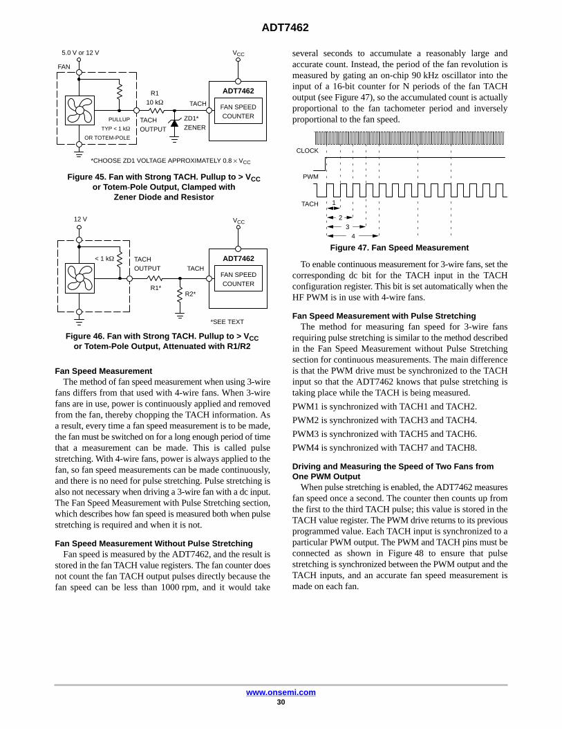
ADT7462
www.onsemi.com30
Figure 45. Fan with Strong TACH. Pullup to > VCCor Totem-Pole Output, Clamped with
Zener Diode and Resistor
5.0 V or 12 V VCC
FAN SPEEDCOUNTER
TACH
ADT7462
*CHOOSE ZD1 VOLTAGE APPROXIMATELY 0.8 × VCC
PULLUP
TYP < 1 k�
OR TOTEM-POLE
ZD1*ZENER
TACHOUTPUT
FAN
R110 k�
Figure 46. Fan with Strong TACH. Pullup to > VCCor Totem-Pole Output, Attenuated with R1/R2
12 V VCC
FAN SPEEDCOUNTER
TACH
ADT7462
*SEE TEXT
< 1 k�
R1*R2*
TACHOUTPUT
Fan Speed MeasurementThe method of fan speed measurement when using 3-wire
fans differs from that used with 4-wire fans. When 3-wirefans are in use, power is continuously applied and removedfrom the fan, thereby chopping the TACH information. Asa result, every time a fan speed measurement is to be made,the fan must be switched on for a long enough period of timethat a measurement can be made. This is called pulsestretching. With 4-wire fans, power is always applied to thefan, so fan speed measurements can be made continuously,and there is no need for pulse stretching. Pulse stretching isalso not necessary when driving a 3-wire fan with a dc input.The Fan Speed Measurement with Pulse Stretching section,which describes how fan speed is measured both when pulsestretching is required and when it is not.
Fan Speed Measurement Without Pulse StretchingFan speed is measured by the ADT7462, and the result is
stored in the fan TACH value registers. The fan counter doesnot count the fan TACH output pulses directly because thefan speed can be less than 1000 rpm, and it would take
several seconds to accumulate a reasonably large andaccurate count. Instead, the period of the fan revolution ismeasured by gating an on-chip 90 kHz oscillator into theinput of a 16-bit counter for N periods of the fan TACHoutput (see Figure 47), so the accumulated count is actuallyproportional to the fan tachometer period and inverselyproportional to the fan speed.
Figure 47. Fan Speed Measurement
CLOCK
PWM
TACH 1
23
4
To enable continuous measurement for 3-wire fans, set thecorresponding dc bit for the TACH input in the TACHconfiguration register. This bit is set automatically when theHF PWM is in use with 4-wire fans.
Fan Speed Measurement with Pulse StretchingThe method for measuring fan speed for 3-wire fans
requiring pulse stretching is similar to the method describedin the Fan Speed Measurement without Pulse Stretchingsection for continuous measurements. The main differenceis that the PWM drive must be synchronized to the TACHinput so that the ADT7462 knows that pulse stretching istaking place while the TACH is being measured.
PWM1 is synchronized with TACH1 and TACH2.
PWM2 is synchronized with TACH3 and TACH4.
PWM3 is synchronized with TACH5 and TACH6.
PWM4 is synchronized with TACH7 and TACH8.
Driving and Measuring the Speed of Two Fans fromOne PWM Output
When pulse stretching is enabled, the ADT7462 measuresfan speed once a second. The counter then counts up fromthe first to the third TACH pulse; this value is stored in theTACH value register. The PWM drive returns to its previousprogrammed value. Each TACH input is synchronized to aparticular PWM output. The PWM and TACH pins must beconnected as shown in Figure 48 to ensure that pulsestretching is synchronized between the PWM output and theTACH inputs, and an accurate fan speed measurement ismade on each fan.

ADT7462
www.onsemi.com31
Figure 48. Synchronizing Fan PWM Output and TACH Inputs
FAN 1
PWM2PWM1
PWM3 PWM4
FAN 2 FAN 3 FAN 4
FAN 5 FAN 6 FAN 7 FAN 8
TACH 1 TACH 2 TACH 3 TACH 4
TACH 5 TACH 6 TACH 7 TACH 8
Driving and Measuring the Speed of One Fan fromOne PWM Output
If four single fans are being controlled and measured bythe ADT7462, the following configuration should be used.This applies only to 3-wire fans controlled using lowfrequency PWM with pulse stretching enabled.
Fan 1 is driven by PWM1 and measured using TACH1.
Fan 2 is driven by PWM2 and measured using TACH3.
Fan 3 is driven by PWM3 and measured using TACH5.
Fan 4 is driven by PWM4 and measured using TACH7.
Figure 49. Driving and Measuring the Speed on aSingle Fan
FAN 1
PWM2PWM1
PWM3 PWM4
FAN 2
FAN 3 FAN 4
TACH 1 TACH 3
TACH 5 TACH 7
The PWM output is pulse stretched until a valid TACH isread on both TACH inputs synchronized to the particularPWM output. If one fan is connected to one PWM output,the PWM output is pulse stretched until the counter hastimed out on the disconnected TACH input. In this case, thepulse is stretching longer than necessary in an effort to sensea disconnected fan. The speed of the connected fan may beincreased and an audible change in fan speed may beobserved. There are two options to prevent the PWM outputfrom being stretched longer than necessary in this case.• Connect the two synchronized TACH inputs together;
for example, if PWM1 is driving a single fan being
sensed on TACH1 only, connect TACH1 and TACH2together.
• Turn off pulse stretching on the unused TACH input;that is, if PWM1 is driving a single fan being sensed onTACH1 only, turn off pulse stretching on TACH2 inRegister 0x08. In this register:
Bit 0 controls pulse stretching on TACH1 and TACH5.
Bit 1 controls pulse stretching on TACH2 and TACH6.
Bit 2 controls pulse stretching on TACH3 and TACH7.
Bit 3 controls pulse stretching on TACH4 and TACH8.
Note that the TACH assignments in this register differfrom the TACHs synchronized to each PWM output.Therefore, if the intention is to drive and sense four fans,connecting the TACHs together as described in Option 1allows pulse stretching on all channels.
To enable fan speed measurements four times a second,set the FAST bit (Bit 0) of Configuration Register 2 (0x02).When the FAST bit is set, fan TACH readings are updatedevery 250 ms.
Fan Speed Measurement RegistersFan speed measurement involves a 2-register read for
each measurement. The low byte should be read first. Thiscauses the high byte to be frozen until both high and low byteregisters have been read, preventing erroneous TACHreadings. The fan tachometer reading registers report backthe number of 11.11 �s period clocks (90 kHz oscillator)gated to the fan speed counter, from the rising edge of thefirst fan TACH pulse to the rising edge of the third fan TACHpulse (because two pulses per revolution are being counted).Because the device is essentially measuring the fan TACHperiod, the higher the count value, the slower the fan isactually running. A 16-bit fan tachometer reading of0xFFFF indicates either that the fan has stalled or is runningvery slowly (< 100 rpm).
The actual fan TACH period is being measured; therefore,an ALERT is generated if the reading falls below a fanTACH limit. This ALERT sets the appropriate status bit andcan be used to generate an SMBALERT. The TACH limit isan 8-bit value that is compared with the TACH high byte ofthe TACH reading.
Table 25. TACHOMETER VALUE & LIMIT REGISTERS
TACHLow Byte
Value RegisterHigh Byte
Value Register8-bit LimitRegister
TACH1 0x98 0x99 0x78
TACH2 0x9A 0x9B 0x79
TACH3 0x9C 0x9D 0x7A
TACH4 0x9E 0x9F 0x7B
TACH5 0xA2 0xA3 0x7C
TACH6 0xA4 0xA5 0x7D
TACH7 0xA6 0xA7 0x7E
TACH8 0xA8 0xA9 0x7F

ADT7462
www.onsemi.com32
Calculating Fan SpeedAssuming a fan with two pulses per revolution (and two
pulses per revolution being measured), fan speed iscalculated by:
Fan Speed(RPM) � (freq � 60)�Fan Tachometer Reading
(eq. 1)
where:Fan Tachometer Reading is the 16-bit fan tachometerreading. freq is the oscillator frequency, 90 kHz.
Example:
TACH1 high byte (Register 0x99) = 0x17
TACH1 low byte (Register 0x98) = 0xFF
What is the speed of Fan 1 in rpm?
Fan 1 Tachometer Reading � 0 � 17FF � 6143 Decimal(eq. 2)
RPM � (freq � 60)�Fan 1 Tachometer Reading (eq. 3)
Fan Speed � 879 RPM
(eq. 4)RPM � (90000 � 60)�6143
(eq. 5)
If the fan is a 6-pole fan, the count value is representativeof 2/3 of a revolution. Therefore, the result of Equation 5should be divided by 1.5. Similarly, if the fan used is an8-pole fan, then the result should be divided by 2.
Fan Spin-UpThe ADT7462 has a unique fan spin-up function. It spins
the fan at 100% PWM duty cycle until two TACH pulses aredetected on the TACH input. Once two TACH pulses havebeen detected, the PWM duty cycle goes to the expectedrunning value, for example, 33%. The advantage of thisprocess is that fans have different spin-up characteristics andrequire different times to overcome inertia. The ADT7462runs the fans just fast enough to overcome inertia and thefans are quieter on spin-up than fans programmed to spin upfor a given spin-up time.
Fan Startup TimeoutTo prevent false interrupts being generated as a fan spins
up (because it is below running speed), the ADT7462includes a fan startup timeout function. During this time, theADT7462 looks for two TACH pulses. If two TACH pulsesare not detected, an interrupt is generated. UsingConfiguration Register 1 (0x01), Bit 4, this functionalitycan be changed to spinning the fans for a programmable timeinstead of two TACH pulses.
The startup timeout for each PWM drive is programmedby Bits [2:0] in the PWMx configuration registers.
PWM1 Configuration Register = Register 0x21
PWM2 Configuration Register = Register 0x22
PWM3 Configuration Register = Register 0x23
PWM4 Configuration Register = Register 0x24
Table 26. FAN STARTUP TIMEOUT
Bit Code Startup Timeout
000 No Startup Timeout
001 100 ms
010 250 ms
011 400 ms
100 667 ms
101 1 sec
110 2 sec
111 32 sec
PWM Logic StateThe PWM outputs can be programmed high for 100%
duty cycle (non-inverted) or low for 100% duty cycle(inverted). This is programmed for each PWM drive in thePWMx Configuration Registers using the INV bit (Bit 4).
0 = Active high PWM outputs.
1 = Active low PWM outputs.
Low Frequency Mode PWM Drive FrequencyThe PWM drive frequency can be adjusted for the
application. The ADT7462 supports both high frequencyand low frequency PWM. High or low frequency PWMmode is selected in Register 0x02, Bit 2. In high frequencymode, the PWM drive frequency is always 22.5 kHz andcannot be changed. Register 0x25 and Register 0x26configure the PWM frequency in low frequency mode forPWM1 to PWM4.
PWM Drive Frequency 1 is set using Bits [4:2] of thePWM1 and PWM2 frequency register (0x25).
PWM Drive Frequency 2 is set using Bits [7:5] of thePWM1 and PWM2 frequency register (0x25).
PWM Drive Frequency 3 is set using Bits [4:2] of thePWM3 and PWM4 frequency register (0x26).
PWM Drive Frequency 4 is set using Bits [7:5] of thePWM3 and PWM4 frequency register (0x26).
Table 27. LOW FREQUENCY PWM OPTIONS
Bit Code Frequency
000 11 Hz
001 14.7 Hz
010 22.1 Hz
011 29.4 Hz
100 35.3 Hz
101 44.1 Hz
110 58.8 Hz
111 88.2 Hz

ADT7462
www.onsemi.com33
Fan Speed ControlThe ADT7462 controls fan speed using two different
modes: automatic and manual.In automatic fan speed control mode, fan speed is
automatically varied with temperature and without CPUintervention, after initial parameters are set up. Theadvantage of this mode is that if the system hangs, the systemis protected from overheating. The automatic fan speedcontrol incorporates a feature called dynamic TMINcalibration. This feature reduces the design effort requiredto program the automatic fan speed control loop. For moreinformation on how to program the automatic fan speedcontrol loop and dynamic TMIN operation, see theProgramming the Automatic Fan Speed Control Loopsection.
In manual fan speed control mode, the ADT7462 allowsthe duty cycle of any PWM output to be manually adjusted.This is useful if the user wants to change fan speed in thesoftware or adjust PWM duty cycle output for test purposes.Bits [7:5] of Register 0x21 to Register 0x24 (PWMconfiguration registers) control the behavior of each PWMoutput. Under manual control, each PWM output can bemanually updated by writing to Register 0xAA toRegister 0xAD (PWM duty cycle registers).
Programming the PWM Current Duty Cycle RegistersThe PWM current duty cycle registers are 8-bit registers
that allow the PWM duty cycle for each output to be setanywhere from 0% to 100% in steps of 0.39%.
The value to be programmed into the PWMMIN register isgiven by:
Value (decimal) = PWMMIN/0.39
Example 1: For a PWM duty cycle of 50%,Value (decimal) = 50/0.39 = 128 decimalValue = 128 decimal or 0x80
Example 2: For a PWM duty cycle of 33%,Value (decimal) = 33/0.39 = 85 decimalValue = 84 decimal or 0x54
PWM Duty Cycle Registers
Register 0xAA PWM1 Duty Cycle = 0x00 (0% default)
Register 0xAB PWM2 Duty Cycle = 0x00 (0% default)
Register 0xAC PWM3 Duty Cycle = 0x00 (0% default)
Register 0xAD PWM4 Duty Cycle = 0x00 (0% default)
By reading the PWMx current duty cycle registers, theuser can keep track of the current duty cycle on each PWMoutput, even when the fans are running in automatic fanspeed control mode or acoustic enhancement mode.
Figure 50. Control PWM Duty Cycle Manually with aResolution of 0.39%
VARY PWM DUTYCYCLE WITH 8-BITRESOLUTION
Programming the Automatic Fan Speed Control LoopNote that to better understand the automatic fan speed
control loop, use of the ADT7462 evaluation board andsoftware is strongly recommended while reading thissection.
This section provides the system designer with anunderstanding of the automatic fan control loop andprovides step-by-step guidance on effectively evaluatingand selecting critical system parameters. To optimizesystem characteristics, the designer needs to carefully plansystem configuration, including the number of fans, wherethey are located, and what temperatures are being measuredin the particular system.
The mechanical or thermal engineer who is tasked withthe system thermal characterization should also be involvedat the beginning of the process.
Automatic Fan Control OverviewThe ADT7462 can automatically control the speed of fans
based upon the measured temperature. This is doneindependently from CPU intervention once initial parametersare set up.
The ADT7462 has a local temperature sensor and up tothree remote temperature channels that can be connected toa CPU on-chip thermal diode (available on Intel Pentiumclass and other CPUs/GPUs). These four temperaturechannels can be used as the basis for automatic fan speedcontrol to drive fans using pulse-width modulation (PWM).
Automatic fan speed control reduces acoustic noise byoptimizing fan speed according to accurately measuredtemperature. Reducing fan speed can also decrease systemcurrent consumption. The automatic fan speed control modeis very flexible, owing to the number of programmableparameters, including TMIN and TRANGE. The TMIN and

ADT7462
www.onsemi.com34
TRANGE values for a temperature channel and, therefore, fora given fan, are critical because they define the thermalcharacteristics of the system. The thermal validation of thesystem is one of the most important steps in the designprocess, so these values should be selected carefully.
Figure 51 gives a top-level overview of the automatic fancontrol circuitry on the ADT7462. From a systems-levelperspective, up to four system temperatures can bemonitored and used to control four PWM outputs. The fourPWM outputs can be used to control up to eight fans. TheADT7462 allows the speed of eight fans to be monitored.The Remote 1 and Remote 2 temperature channels have athermal calibration block, allowing the designer to
individually configure the thermal characteristics of thosetemperature channels. For example, the CPU fan can be runwhen CPU temperature increases above 60°C and a chassisfan can be run when the local temperature increases above45°C. At this stage, the designer has not assigned thesethermal calibration settings to a particular fan drive (PWM)channel. The right side of Figure 51 shows controls that arefan-specific. The designer has control over individualparameters such as minimum PWM duty cycle, fan speedfailure thresholds, and even ramp control of the PWMoutputs. Automatic fan control, then, ultimately allowsgraceful fan speed changes that are less perceptible to thesystem user.
Figure 51. Automatic Fan Control Block Diagram
THERMAL CALIBRATION
REMOTE1TEMP
100%
0%TMIN TRANGE
THERMAL CALIBRATION
100%
0%TMIN TRANGE
THERMAL CALIBRATION
100%
0%TMIN TRANGE
LOCALTEMP
REMOTE2TEMP
PWMMIN
PWMMIN
PWMMIN
MUX
�
�
�
PWMCONFIG
PWMGENERATOR
PWMCONFIG
PWMGENERATOR
PWMCONFIG
PWMGENERATOR
PWM1
PWM2
PWM3
TACH1
TACH2
TACH3
RAMPCONTROL
(ACOUSTICENHANCEMENT)
TACHOMETER 1MEASUREMENT
RAMPCONTROL
(ACOUSTICENHANCEMENT)
TACHOMETER 2MEASUREMENT
RAMPCONTROL
(ACOUSTICENHANCEMENT)
TACHOMETER 3AND 4
MEASUREMENT
Step 1 − Configuring the MUXFirst, the user needs to decide how many temperature
channels are being measured and how many fans need to becontrolled and monitored. When these decisions have beenmade, the fans can be assigned to particular temperaturechannels. Not only can fans be assigned to individualchannels, but the behavior of the fans is also configurable.For example, fans can be run under automatic fan control;they can be run manually (under software control) or theycan be run at the fastest speed calculated by multipletemperature channels. The MUX is the bridge betweentemperature measurement channels and the three PWMoutputs.
Bits [7:5] (BHVR) of Register 0x21, Register 0x22,Register 0x23, and Register 0x24 (PWM configurationregisters) control the behavior of the fans connected to the
PWM1, PWM2, PWM3, and PWM4 outputs. The valuesselected for these bits determine how the MUX connects atemperature measurement channel to a PWM output (seeFigure 52).
Automatic Fan Control MUX OptionsBits [7:5] (BHVR), of Register 0x21, Register 0x22,
Register 0x23, and Register 0x24, control the behavior of thecorresponding PWM outputs (see Table 61 and Table 62).
The fastest speed calculated options pertain to controllingone PWM output based on multiple temperature channels.The thermal characteristics of the three temperature zonescan be set to drive a single fan. An example is the fan turningon when the Remote 1 temperature exceeds 60°C or whenthe local temperature exceeds 45°C.

ADT7462
www.onsemi.com35
Step 2 − TMIN Settings for Thermal CalibrationChannels
TMIN is the temperature at which the fans start to turn onunder automatic fan control. The speed at which the fan runsat TMIN is programmed later. The TMIN values chosen aretemperature channel-specific; for example, 25°C forambient channel, 30°C for VRM temperature, and 40°C forprocessor temperature.
TMIN is an 8-bit value, either twos complement or Offset64, that can be programmed in 1°C increments. There is aTMIN register associated with each temperature measurementchannel: local, Remote 1, Remote 2, and Remote 3. When theTMIN value is exceeded, the fan turns on and runs at theminimum PWM duty cycle. The fan turns off after thetemperature has dropped below TMIN − THYST.
Figure 52. Assigning Temperature Channels to Fan Channels
THERMAL CALIBRATION
REMOTE1 =AMBIENT TEMP
100%
0%TMIN TRANGE
PWMMIN
MUX
�
PWMCONFIG
PWMGENERATOR
RAMPCONTROL
(ACOUSTICENHANCEMENT)
TACHOMETER1MEASUREMENT
MUX
�
�
PWMMIN
PWMMIN
THERMAL CALIBRATION100%
0%TMIN TRANGE
THERMAL CALIBRATION100%
0%TMIN TRANGE
LOCAL =VRM TEMP
REMOTE2 =CPU TEMP
RAMPCONTROL
(ACOUSTICENHANCEMENT)
TACHOMETER2MEASUREMENT
RAMPCONTROL
(ACOUSTICENHANCEMENT)
TACHOMETER3AND 4
MEASUREMENT
PWMCONFIG
PWMGENERATOR
PWMCONFIG
PWMGENERATOR
PWM1
PWM2
PWM3
TACH3
TACH2
TACH1
CPU FAN SINK
FRONT CAHSSIS
REAR CAHSSIS
To overcome fan inertia, the fan is spun up until two validTACH rising edges are counted. See the Fan Spin-Upsection for more details. In some cases, primarily forpsycho-acoustic reasons, the fan should never switch offbelow TMIN. The corresponding bits in Register 0x25 andRegister 0x26 should be set to keep the fans running at thePWM minimum duty cycle, if the temperature falls belowTMIN.
TMIN Registers
Register 0x5C, Local Temperature TMIN = 0x9A (90°C)
Register 0x5D, Remote 1 Temperature TMIN = 0x9A (90°C)
Register 0x5E, Remote 2 Temperature TMIN = 0x9A (90°C)
Register 0x5F, Remote 3 Temperature TMIN = 0x9A (90°C)
PWM1 and PWM2 Frequency Register (0x25)
Bit 0 (MIN 1) = 0. PWM1 is off (0% PWM duty cycle)when temperature is below TMIN − THYST.
Bit 0 (MIN 1) = 1. PWM1 runs at PWM1 minimum dutycycle below TMIN − THYST.
Bit 1 (MIN 2) = 0. PWM2 is off (0% PWM duty cycle) whentemperature is below TMIN − THYST.
Bit 1 (MIN 2) = 1. PWM2 runs at PWM2 minimum dutycycle below TMIN − THYST.
PWM3 and PWM4 Frequency Register (0x26)
Bit 0 (MIN 3) = 0. PWM3 is off (0% PWM duty cycle) whentemperature is below TMIN − THYST.
Bit 0 (MIN 3) = 1. PWM3 runs at PWM3 minimum dutycycle below TMIN − THYST.
Bit 1 (MIN 4) = 0. PWM4 is off (0% PWM duty cycle) whentemperature is below TMIN − THYST.
Bit 1 (MIN 4) = 1. PWM4 runs at PWM4 minimum dutycycle below TMIN − THYST.

ADT7462
www.onsemi.com36
Figure 53. Understanding the TMIN Parameter
THERMAL CALIBRATION
REMOTE2 =CPU TEMP
100%
0%TMIN TRANGE
PWMMIN
MUX
�
PWMCONFIG
PWMGENERATOR
RAMPCONTROL
(ACOUSTICENHANCEMENT)
TACHOMETER1MEASUREMENT
�
�
PWMMIN
PWMMIN
THERMAL CALIBRATION100%
0%TMIN TRANGE
THERMAL CALIBRATION100%
0%TMIN TRANGE
LOCAL =VRM TEMP
REMOTE1 =AMBIENT TEMP
RAMPCONTROL
(ACOUSTICENHANCEMENT)
TACHOMETER2MEASUREMENT
RAMPCONTROL
(ACOUSTICENHANCEMENT)
TACHOMETER3AND 4
MEASUREMENT
PWMCONFIG
PWMGENERATOR
PWMCONFIG
PWMGENERATOR
PWM1
PWM2
PWM3
TACH3
TACH2
TACH1
CPU FAN SINK
FRONT CAHSSIS
REAR CAHSSIS
TMIN
100%
0%P
WM
DU
TY
CY
CLE
Step 3 − PWMMIN for Each PWM (Fan) OutputPWMMIN is the minimum PWM duty cycle at which each
fan in the system runs. It is also the start speed for each fanunder automatic fan control when the temperature risesabove TMIN. For maximum system acoustic benefit,PWMMIN should be as low as possible. Depending on thefan used, the PWMMIN setting is usually in the 20% to 33%duty cycle range. This value can be found through fanvalidation.
Figure 54. PWMMIN Determines MinimumPWM Duty Cycle
TMIN
100%
0%
PW
M D
UT
Y C
YC
LE
TEMPERATURE
PWMMIN
More than one PWM output can be controlled from asingle temperature measurement channel. For example,
Remote 1 temperature can control PWM1 and PWM2outputs. If two different fans are used on PWM1 and PWM2,the fan characteristics can be set up differently. As a result,Fan 1, driven by PWM1, can have a different PWMMINvalue than that of Fan 2 connected to PWM2. Figure 55illustrates this as PWM1MIN (the front fan) turns on at aminimum duty cycle of 20%, while PWM2MIN (the rear fan)turns on at a minimum duty cycle of 40%. Note, however,that both fans turn on at exactly the same temperature,defined by TMIN.
Figure 55. Operating Two Different Fans from aSingle Temperature Channel
TMIN
100%
0%
TEMPERATURE
PWM1MIN
PWM2MIN PWM1
PWM2
PW
M D
UT
Y C
YC
LE

ADT7462
www.onsemi.com37
Programming the PWMMIN RegistersThe PWMMIN registers are 8-bit registers that allow the
minimum PWM duty cycle for each output to be configuredanywhere from 0% to 100%. This allows the minimumPWM duty cycle to be set in steps of 0.39%.
The value to be programmed into the PWMMIN register isgiven by:
Value (decimal) = PWMMIN /0.39
Example 1: For a minimum PWM duty cycle of 50%,Value (decimal) = 50/0.39 = 128 (decimal)Value = 128 (decimal) or 0x80 (hexadecimal)
Example 2: For a minimum PWM duty cycle of 33%,Value (decimal) = 33/0.39 = 85 (decimal)Value = 85 (decimal) or 0x54 (hexadecimal)
PWMMIN Registers
Register 0x28, Minimum PWM1 Duty Cycle = 0x80(50% Default)
Register 0x29, Minimum PWM2 Duty Cycle = 0x80(50% Default)
Register 0x2A, Minimum PWM3 Duty Cycle = 0x80(50% Default)
Register 0x2B, Minimum PWM4 Duty Cycle = 0x80(50% Default)
Note on Fan Speed and PWM Duty CycleThe PWM duty cycle does not directly correlate to fan
speed in rpm. Running a fan at 33% PWM duty cycle doesnot equate to running the fan at 33% speed. Driving a fan at33% PWM duty cycle actually runs the fan at closer to 50%of its full speed. This is because fan speed in % rpmgenerally relates to the square root of PWM duty cycle.Given a PWM square wave as the drive signal, fan speed inrpm approximates to:
% fanspeed � PWM duty cycle � 10�
Step 4 − PWMMAX for PWM (Fan) OutputsPWMMAX is the maximum duty cycle that each fan in the
system runs at under the automatic fan speed control loop.For maximum system acoustic benefit, PWMMAX should beas low as possible but should be capable of maintaining theprocessor temperature limit at an acceptable level. If theTHERM temperature limit is exceeded, the fans are stillboosted to 100% for fail-safe cooling.
There is one PWMMAX limit (Register 0x2C) for all fanchannels.
Figure 56. PWMMAX Determines Maximum PWM DutyCycle Below the THERM Temperature Limit
TMIN
100%
0%
TEMPERATURE
PWMMIN
PWMMAX
PW
M D
UT
Y C
YC
LE
Programming the PWMMAX RegisterThe PWMMAX register (0x2C) is an 8-bit register that
allows the maximum PWM duty cycle for the outputs to beconfigured anywhere from 0% to 100%. This allows themaximum PWM duty cycle to be set in steps of 0.39%.
The value to be programmed into the PWMMAX registeris given by:
Value (decimal) = PWMMAX/0.39
Example 1: For a maximum PWM duty cycle of 50%,Value (decimal) = 50/0.39 = 128 (decimal)Value = 128 (decimal) or 0x80 (hexadecimal)
Example 2: For a maximum PWM duty cycle of 75%,Value (decimal) = 75/0.39 = 192 (decimal)Value = 192 (decimal) or 0xC0 (hexadecimal)
PWMMAX Register
Register 0x2C, Maximum PWM1 to PWM4 DutyCycle = 0xC0 (75% default)
See the Note on Fan Speed and PWM Duty Cycle sectionfor more information.
Step 5 − TRANGE for Temperature ChannelsTRANGE is the range of temperatures over which
automatic fan control occurs when the programmed TMINtemperature is exceeded. TRANGE is a temperature slope, notan arbitrary value; that is, a TRANGE of 40°C holds true onlyfor PWMMIN = 33%. If PWMMIN is increased or decreased,the effective TRANGE changes.
Figure 57. TRANGE Parameter Affects Cooling Slope
TMIN
100%
0%
TEMPERATURE
PWMMIN
PW
M D
UT
Y C
YC
LE
TRANGE

ADT7462
www.onsemi.com38
The TRANGE or fan control slope is determined by thefollowing procedure:
1. Determine the maximum operating temperature forthat channel (for example, 70°C).
2. Determine experimentally the fan speed (PWMduty cycle value) that does not exceed thetemperature at the worst-case operating points.(For example, 70°C is reached when the fans arerunning at 50% PWM duty cycle.)
3. Determine the slope of the required control loop tomeet these requirements.
4. Using the ADT7462 evaluation software, thisfunctionality can be graphically programmed andvisualized.
Figure 58. Adjusting PWMMIN Affects TRANGE
TMIN
100%
0%
30°C
PW
M D
UT
Y C
YC
LE
33%
50%
40°C
TRANGE is implemented as a slope, which means that asPWMMIN is changed, TRANGE changes, but the actual sloperemains the same. The higher the PWMMIN value, thesmaller the effective TRANGE; that is, the fan reaches fullspeed (100%) at a lower temperature.
Figure 59. Increasing PWMMIN Changes EffectiveTRANGE
TMIN
100%
0%
30°C
PW
M D
UT
Y C
YC
LE
10%25%33%50%
40°C45°C
54°C
For a given TRANGE value, the temperature at which thefan runs at full speed for different PWMMIN values can beeasily calculated by:
TMAX = TMIN + (Max DC − Min DC) × TRANGE/170
where:TMAX is the temperature at which the fan runs full speed.TMIN is the temperature at which the fan turns on.Max DC is the maximum duty cycle (100%) = 255 decimal.Min DC is equal to PWMMIN.TRANGE is the PWM duty cycle vs. temperature slope.
Example 1Calculate TMAX, given that TMIN = 30°C, TRANGE = 40°C,
and PWMMIN = 10% duty cycle = 26 (decimal).
TMAX = TMIN + (Max DC − Min DC) × TRANGE/170TMAX = 30°C + (100% − 10%) × 40°C/170TMAX = 30°C + (255 − 26) × 40°C/170TMAX = 84°C (effective TRANGE = 54°C)
Example 2Calculate TMAX, given that TMIN = 30°C, TRANGE = 40°C,
and PWMMIN = 25% duty cycle = 64 (decimal).
TMAX = TMIN + (Max DC − Min DC) × TRANGE/170TMAX = 30°C + (100% − 25%) × 40°C/170TMAX = 30°C + (255 − 64) × 40°C/170TMAX = 75°C (effective TRANGE = 45°C)
Example 3Calculate TMAX, given that TMIN = 30°C, TRANGE = 40°C,
and PWMMIN = 33% duty cycle = 85 (decimal).
TMAX = TMIN + (Max DC − Min DC) × TRANGE/170TMAX = 30°C + (100% − 33%) × 40°C/170TMAX = 30°C + (255 − 85) × 40°C/170TMAX = 70°C (effective TRANGE = 40°C)
Example 4Calculate TMAX, given that TMIN = 30°C, TRANGE = 40°C,
and PWMMIN = 50% duty cycle = 128 (decimal).
TMAX = TMIN + (Max DC − Min DC) × TRANGE/170TMAX = 30°C + (100% − 50%) × 40°C/170TMAX = 30°C + (255 − 128) × 40°C/170TMAX = 60°C (effective TRANGE = 30°C)
Selecting a TRANGE SlopeThe TRANGE value can be selected for each temperature
channel: local, Remote 1, Remote 2, and Remote 3.Bits [7:4] (RANGE) of Register 0x60 to Register 0x63define the TRANGE value for each temperature channel (seeTable 85 and Table 86).
Summary of TRANGE FunctionWhen using the automatic fan control function, the
temperature at which the fan reaches full speed can becalculated by:
TMAX � TMIN � TRANGE (eq. 6)
Equation 6 holds true only when PWMMIN is equal to33% PWM duty cycle.
Increasing or decreasing PWMMIN changes the effectiveTRANGE, although the fan control still follows the samePWM duty cycle to temperature slope. The effective

ADT7462
www.onsemi.com39
TRANGE for different PWMMIN values can be calculatedusing Equation 7.
(eq. 7)
TMAX � TMIN � (Max DC � Min DC) � TRANGE�170
where (Max DC − Min DC) × TRANGE/170 is the effectiveTRANGE value.
Figure 60 shows PWM duty cycle vs. temperature foreach TRANGE setting. The lower graph shows how eachTRANGE setting affects fan speed vs. temperature. As shownin the graph, the effect on fan speed is nonlinear.
20
30
40
50
60
70
80
Figure 60. TRANGE vs. Actual Fan Speed Profile
2�C
80�C
53.3�C
40�C
32�C
26.6�C
20�C
16�C
13.3�C
10�C
8�C
6.67�C
5�C
4�C
3.33�C
2.5�C
2�C
80�C
53.3�C
40�C
32�C
26.6�C
20�C
16�C
13.3�C
10�C
8�C
6.67�C
5�C
4�C
3.33�C
2.5�C
TEMPERATURE ABOVE TMIN
0
PW
M D
UT
Y C
YC
LE (
%)
020 40 60 80 100 120
10
20
30
40
50
60
70
80
90
100
TEMPERATURE ABOVE TMIN
FAN
SP
EE
D (
% O
F M
AX
)
020 40 60 80 100 120
10
90
100
0
The graphs in Figure 60 assume that the fan starts from0% PWM duty cycle. Clearly, the minimum PWM dutycycle, PWMMIN, needs to be factored in to see how the loopactually performs in the system. Figure 61 shows howTRANGE is affected when the PWMMIN value is set to 20%.It can be seen that the fan runs about 45% fan speed when thetemperature exceeds TMIN.
Example: Determining TRANGE for Each TemperatureChannel
The following example shows how the different TMIN andTRANGE settings can be applied to three different thermalzones. In this example, the following TRANGE values apply:
TRANGE = 80°C for Ambient TemperatureTRANGE = 53.3°C for CPU TemperatureTRANGE = 40°C for VRM Temperature
Figure 61. TRANGE vs. % Fan Speed Slopes withPWMMIN = 20%
2�C
80�C
53.3�C
40�C
32�C
26.6�C
20�C
16�C
13.3�C
10�C
8�C
6.67�C
5�C
4�C
3.33�C
2.5�C
2�C
80�C
53.3�C
40�C
32�C
26.6�C
20�C
16�C
13.3�C
10�C
8�C
6.67�C
5�C
4�C
3.33�C
2.5�C
TEMPERATURE ABOVE TMIN
0
PW
M D
UT
Y C
YC
LE (
%)
020 40 60 80 100 120
10
20
30
40
50
60
70
80
90
100
20
30
40
50
60
70
80
TEMPERATURE ABOVE TMIN
FAN
SP
EE
D (
% O
F M
AX
)
020 40 60 80 100 120
10
90
100
0
This example uses the MUX configuration described inthe Step 1 − Configuring the MUX section. Both CPUtemperature and VRM temperature drive the CPU fanconnected to PWM1. Ambient temperature drives the frontchassis fan and rear chassis fan connected to PWM2 andPWM3.
The front chassis fan is configured to run atPWMMIN = 20%. The rear chassis fan is configured to runat PWMMIN = 30%. The CPU fan is configured to run atPWMMIN = 10%.

ADT7462
www.onsemi.com40
Note on 4-wire FansThe control range for 4-wire fans is much wider than that
of 2-wire or 3-wire fans. In many cases, 4-wire fans can startwith a PWM drive of as little as 20%.
Figure 62. TRANGE and % Fan Speed Slopes for VRM,Ambient, and CPU Temperature Channels
TEMPERATURE ABOVE TMIN
0
PW
M D
UT
Y C
YC
LE (
%)
010 20 30 40 50 60 70 80 90 100
10
20
30
40
50
60
70
80
90
100
TEMPERATURE ABOVE TMIN
0
FAN
SP
EE
D (
% M
AX
RP
M)
010 20 30 40 50 60 70 80 90 100
10
20
30
40
50
60
70
80
90
100
Step 6 − TTHERM for Temperature ChannelsTTHERM is the absolute maximum temperature allowed
on a temperature channel. Above this temperature, acomponent such as the CPU or VRM might be operatingbeyond its safe operating limit. When the measuredtemperature exceeds TTHERM, all fans are driven at 100%PWM duty cycle (full speed) to provide critical systemcooling. The fans remain running at 100% until thetemperature drops below TTHERM minus hysteresis, wherehysteresis is the number programmed into Local/Remote 1Hysteresis Register 0x54 and Remote 2/Remote 3Hysteresis Register 0x55. The default hysteresis value is4°C.
The TTHERM limit should be considered as the maximumworst-case operating temperature of the system. Becauseexceeding any TTHERM limit runs all fans at 100%, it hasvery negative acoustic effects. Ultimately, this limit shouldbe set up as a fail-safe, and it must not be exceeded undernormal system operating conditions.
Note that the TTHERM limits cannot be masked, and theyaffect the fan speed no matter how the automatic fan controlsettings are configured. This allows some flexibility becausea TRANGE value can be selected based on its slope, while ahard limit (such as 70°C), can be programmed as TMAX (thetemperature at which the fan reaches full speed) by settingTTHERM to that limit (for example, 70°C).
THERM Registers
Register 0x4C, Local THERM1 temperature limit = 0xA4(100°C Default)
Register 0x4D, Remote 1 THERM1 temperature limit = 0xA4(100°C Default)
Register 0x4E, Remote 2 THERM1 temperature limit = 0xA4(100°C Default)
Register 0x4F Remote 3 THERM1 temperature limit = 0xA4(100°C Default)
Register 0x50, Local THERM2 temperature limit = 0xA4(100°C Default)
Register 0x51, Remote 1 THERM2 temperature limit = 0xA4(100°C Default)
Register 0x52, Remote 2 THERM2 temperature limit = 0xA4(100°C Default)
Register 0x53 Remote 3 THERM2 temperature limit = 0xA4(100°C Default)
Hysteresis Registers
Register 0x54, Local/Remote 1 Temperature HysteresisRegister
Bits [7:4], Local temperature hysteresis (4°C Default)
Bits [3:0], Remote 1 temperature hysteresis (4°C Default)
Register 0x55, Remote 2/Remote 3 TemperatureHysteresis Register
Bits [7:4], Remote 2 temperature hysteresis (4°C Default)
Bits [3:0], Remote 3 temperature hysteresis (4°C Default)
Because each hysteresis setting is four bits, hysteresisvalues are programmable from 1°C to 15°C. It is notrecommended that hysteresis values ever be programmed to0°C, because this value disables hysteresis. In effect, thisvalue causes the fans to cycle between normal speed and100% speed, creating unsettling acoustic noise.
ADT7462
www.onsemi.com41
Figure 63. How TTHERM Relates to Automatic FanControl
TMIN
100%
0%PW
M D
UT
Y C
YC
LE
TTHERM
TRANGE
HYSTERESIS
Step 7 − THYST for Temperature ChannelsTHYST is the amount of extra cooling a fan provides after
the temperature measured has dropped back below TMINbefore the fan turns off. The premise for temperaturehysteresis (THYST) is that without it, the fan would merelychatter or cycle on and off regularly whenever thetemperature hovers near the TMIN setting.
The THYST value chosen determines the amount of timeneeded for the system to cool down or heat up as the fan isturning on and off. Values of hysteresis are programmable inthe range of 1°C to 15°C. Larger values of THYST prevent thefans from chattering on and off. The THYST default value isset at 4°C.
Hysteresis Register
Register 0x60, Bits [3:0] Local HYS
Register 0x61, Bits [3:0] Remote 1 HYS
Register 0x62, Bits [3:0] Remote 2 HYS
Register 0x63, Bits [3:0] Remote 3 HYS
In some applications, it is required that fans not turn offbelow TMIN but remain running at PWMMIN. Bits [1:0] ofthe PWM1, PWM2 Frequency Register (0x25) and thePWM3, PWM4 Frequency Register (0x26) allow the fans tobe turned off or to be kept spinning below TMIN. If the fansare always on, the THYST value has no effect on the fan whenthe temperature drops below TMIN.
Figure 64. THYST Value Applies to Fan On/OffHysteresis
TMIN
100%
0%PW
M D
UT
Y C
YC
LE
TTHERM
TRANGE
THYST
Dynamic TMIN Control ModeIn addition to the automatic fan speed control mode
described in the Automatic Fan Control Overview section,the ADT7462 has a mode that extends the basic automaticfan speed control loop. Dynamic TMIN control allows theADT7462 to intelligently adapt the system’s coolingsolution for best system performance or lowest possiblesystem acoustics, depending on user or design requirements.Use of dynamic TMIN control alleviates the need to designfor worst-case conditions and significantly reduces systemdesign and validation time.
Designing for Worst-Case ConditionsSystem design must always allow for worst-case
conditions. In PC design, the worst-case conditions include,but are not limited to, the following:• Worst-Case Altitude
A computer can be operated at different altitudes.Altitude affects the relative air density, which alters theeffectiveness of the fan cooling solution. For example,when comparing 40°C air temperature at 10,000 feet to20°C air temperature at sea level, relative air density isincreased by 40%. This means that the fan can spin40% slower and make less noise at sea level than at10,000 feet while keeping the system at the sametemperature at both locations.
• Worst-Case FanDue to manufacturing tolerances, fan speeds in rpm arenormally quoted with a tolerance of ±20%. Thedesigner must assume that the fan rpm can be 20%below tolerance. This translates to reduced systemairflow and elevated system temperature. Note that fans20% out of tolerance can negatively impact systemacoustics because they run faster and generate morenoise.
• Worst-Case Chassis AirflowThe same motherboard can be used in a number ofdifferent chassis configurations. The design of thechassis and the physical location of fans andcomponents determine the system’s thermalcharacteristics. Moreover, for a given chassis, theaddition of add-in cards, cables, or other systemconfiguration options can alter the system airflow andreduce the effectiveness of the system cooling solution.The cooling solution can also be inadvertently alteredby the end user. (For example, placing a computeragainst a wall can block the air ducts and reduce systemairflow.)

ADT7462
www.onsemi.com42
Figure 65. Chassis Airflow Issues
FAN
I/O CARDS
POOR CPUAIRFLOW
VENTS
POWERSUPPLY
CPU
DRIVEBAYS
GOOD VENTING =GOOD AIR EXCHANGE
POOR VENTING =POOR AIR EXCHANGE
VENTS
FAN
I/O CARDS
GOOD CPU AIRFLOW
FAN
VENTS
POWERSUPPLY
CPU
DRIVEBAYS
• Worst-Case Processor Power ConsumptionThis data sheet maximum does not necessarily reflectthe true processor power consumption. Designing forworst-case CPU power consumption can result in aprocessor becoming over-cooled (generating excesssystem noise).
• Worst-Case Peripheral Power ConsumptionThe tendency is to design to data sheet maximums forperipheral components (again over-cooling the system).
• Worst-Case AssemblyEvery system manufactured is unique because ofmanufacturing variations. Heat sinks may be loosefitting or slightly misaligned. Too much or too littlethermal grease may be used. Variations in applicationpressure for thermal interface material can affect theefficiency of the thermal solution. Accounting formanufacturing variations in every system is difficult;therefore, the system must be designed for theworst-case.
Figure 66. Thermal Model
SUBSTRATE
HEATSINK
THERMALINTERFACE
MATERIAL
INTEGRATEDHEAT
SPREADER
EPOXYTHERMAL INTERFACE MATERIAL
PROCESSOR
TA
TJ
θCA
θSA
θTIMS
θCTIM
θTIMC
θJTIM
θCS
TC
TTIM
TS
TTIM
θJA
Although a design usually accounts for worst-caseconditions in all these cases, the actual system is almostnever operated at worst-case conditions. The alternative todesigning for the worst case is to use the dynamic TMINcontrol function.
Dynamic TMIN Control OverviewDynamic TMIN control mode builds upon the basic
automatic fan control loop by adjusting the TMIN value
based on system performance and measured temperature.This is important because, instead of designing for the worstcase, the system thermals can be defined as operating zones.The ADT7462 can self-adjust its fan control loop tomaintain either an operating zone temperature or a systemtarget temperature. For example, it can be specified thatambient temperature in a system be maintained at 50°C. Ifthe temperature is below 50°C, the fans might not need to runor might run very slowly. If the temperature is higher than50°C, the fans need to throttle up.
The challenge presented by any thermal design is findingthe right settings to suit the system’s fan control solution.This can involve designing for the worst case, followed byweeks of system thermal characterization and, finally, fanacoustic optimization (for psycho-acoustic reasons).
Obtaining the greatest benefit from the automatic fancontrol mode involves characterizing the system to find thebest TMIN and TRANGE settings for the control loop and thebest PWMMIN value for the quietest fan speed setting. Usingthe ADT7462 dynamic TMIN control mode, however,shortens the characterization time and alleviates tweaking thecontrol loop settings, because the device can self-adjustduring system operation.
Dynamic TMIN control mode is operated by specifying theoperating zone temperatures required for the system.Remote 1 and Remote 2 channels have dedicated operatingpoint registers. This allows the system thermal solution to bebroken down into distinct thermal zones. For example, CPUoperating temperature is 70°C, VRM operating temperatureis 80°C, and ambient operating temperature is 50°C. TheADT7462 dynamically alters the control solution tomaintain each zone temperature as close as possible to itstarget operating point.
Figure 67 shows an overview of the parameters that affectthe operation of the dynamic TMIN control loop.
Figure 67. Dynamic TMIN Control Loop
TMIN
PW
M D
UT
Y C
YC
LE
TEMPERATURE
TLOW
THIGH TRANGE
TTHERMOPERATINGPOINT

ADT7462
www.onsemi.com43
Table 28 provides a brief description of each parameter.
Table 28. TMIN CONTROL LOOP PARAMETERS
Parameter Description
TLOW If the temperature drops below the TLOW limit,an error flag is set in a status register and anSMBALERT interrupt can be generated.
THIGH If the temperature exceeds the THIGH limit, anerror flag is set in a status register and anSMBALERT interrupt can be generated.
TMIN The temperature at which the fan turns onunder automatic fan speed control.
OperatingPoint
The maximum target temperature for aparticular temperature zone. The systemattempts to maintain system temperaturearound the operating point by adjusting theTMIN parameter of the control loop.
TTHERM If the temperature exceeds this critical limit, thefans can be run at 100% for maximum cooling.
TRANGE Programs the PWM duty cycle vs. temperaturecontrol slope.
Dynamic TMIN Control ProgrammingBecause the dynamic TMIN control mode is a basic
extension of the automatic fan control mode, the automaticfan control mode parameters should be programmed first(see Step 1 − Configuring the MUX through Step 8 −Operating Points for Temperature Channels). Then proceedwith dynamic TMIN control mode programming.
Step 8 − Operating Points for Temperature ChannelsThe operating point for each temperature channel is the
optimal temperature for that thermal zone. The hotter eachzone is allowed to be, the quieter the system, because the fansare not required to run as fast. The ADT7462 increases ordecreases fan speeds as necessary to maintain the operatingpoint temperature, allowing for system-to-system variationand removing the need for worst-case design. If a sensibleoperating point value is chosen, any TMIN value can beselected in the system characterization. If the TMIN value istoo low, the fans run sooner than required, and thetemperature is below the operating point. In response, theADT7462 increases TMIN to keep the fans off longer and toallow the temperature zone to get closer to the operatingpoint. Likewise, too high a TMIN value causes the operatingpoint to be exceeded, and in turn, the ADT7462 reduces TMINto turn the fans on sooner to cool the system.
Programming the Operating Point RegistersThere are two operating point registers, one for the
Remote 1 temperature channel and one for the Remote 2temperature channel. These 8-bit registers allow theoperating point temperatures to be programmed with 1°Cresolution.
Operating Point Registers
Register 0x5A, Remote 1 Operating Point = 0xA4(100°C Default)
Register 0x5B, Remote 2 Operating Point = 0xA4(100°C Default)
Operating Point Hysteresis RegisterThe operating point hysteresis register sets the value
below the operating point at which TMIN begins to reduce.
Register 0x64, Bits [7:4] Operating Point Hysteresis = 0x40(4°C Default)
Step 9 − High and Low Limits for TemperatureChannels
The low limit defines the temperature at which the TMINvalue starts to be increased, if temperature falls below thisvalue. This has the net effect of reducing the fan speed,allowing the system to get hotter. An interrupt can begenerated when the temperature drops below the low limit.
The high limit should be set above the operating point butbelow the critical THERM point. An interrupt can begenerated when the temperature rises above the high limit.
How Dynamic TMIN Control WorksThe basic operation of dynamic TMIN control is as
follows:1. Set the target temperature for the temperature
zone, which could be, for example, the Remote 1thermal diode. This value is programmed to theRemote 1 operating point register.
2. As the temperature in that zone rises toward andexceeds the operating point temperature minushysteresis, TMIN is reduced and fan speedincreases.
3. As the temperature drops below the low limitvalue, TMIN is increased and the fan speed isreduced.
Short Cycle and Long CycleThe ADT7462 implements two loops: a short (or
decrease) cycle and a long (or increase) cycle. The shortcycle takes place every n monitoring cycles. The long cycletakes place every 2n monitoring cycles. The value of n isprogrammable for each temperature channel. The bits arelocated at the following register locations.
Dynamic TMIN Control Register 2 (0x0C)
Bits [2:0] (CYR1) = Remote 1
Bits [5:3] (CYR2) = Remote 2

ADT7462
www.onsemi.com44
Table 29. CYCLE BIT ASSIGNMENTS
CodeShortCycle Duration
LongCycle Duration
000 8 cycles 1 sec 16 cycles 2 sec
001 16 cycles 2 sec 32 cycles 4 sec
010 32 cycles 4 sec 64 cycles 8 sec
011 64 cycles 8 sec 128 cycles 16 sec
100 128 cycles 16 sec 256 cycles 32 sec
101 256 cycles 32 sec 512 cycles 64 sec
110 512 cycles 64 sec 1024 cycles 128 sec
111 1024 cycles 128 sec 2048 cycles 256 sec
The cycle time must be chosen carefully. A long cycletime means that TMIN is updated less often. If a system hasvery fast temperature transients, the dynamic TMIN controlloop is always lagging. If a cycle time that is too short ischosen, the full benefit of changing TMIN is not realized andTMIN needs to change again on the next cycle. In effect, it isovershooting. It is necessary to carry out some calibration toidentify the most suitable response time.
Figure 68 shows the steps taken during the short cycle.
Figure 68. Short Cycle Steps
IS T1(n) − T1(n − 1) = 0.5 − 0.75�C
IS T1(n) − T1(n − 1) = 1.0 − 1.75�C
IS T1(n) − T1(n − 1) > 2.0�C
IS T1(n) >(OP1 – HYS)
YES
IS T1(n) – T1(n – 1)≤ 0.25°C
DO NOTHING(SYSTEM
COOLING IS OFFOR CONSTANT)
YES
NO
NODO NOTHING
WAIT nMONITORING
CYCLES
PREVIOUSTEMPERATUREMEASUREMENT
T1 (n – 1)
CURRENTTEMPERATUREMEASUREMENT
T1(n)
OPERATING POINT
TEMPERATUREOP1
DECREASE TMIN BY 1�C
DECREASE TMIN BY 2�C
DECREASE TMIN BY 4�C
Figure 69 shows the steps taken during the long cycle.
Figure 69. Long Cycle Steps
WAIT 2nMONITORING
CYCLES
IS T1(n) < LOW TEMP LIMITAND
TMIN < HIGH TEMP LIMITAND
TMIN < OP1AND
T1(n) > TMIN
IS T1(n) > OP1YES
INCREASETMIN BY 1�C
YES
NO
NO
DECREASE TMINBY 1�C
CURRENTTEMPERATUREMEASUREMENT
T1(n)
OPERATING POINT
TEMPERATUREOP1
DO NOTCHANGE
The following examples illustrate some of thecircumstances that may cause TMIN to increase, decrease, orstay the same.
Example 1: Normal Operation, No TMIN Adjustment1. If the measured temperature never exceeds the
programmed operating point minus the hysteresistemperature, TMIN is not adjusted; that is, itremains at its current setting.
2. If the measured temperature never drops below thelow temperature limit, TMIN is not adjusted.
Figure 70. Temperature Between the Operating Pointand the Low Temperature Limit
THERM LIMIT
HIGH TEMP LIMIT
OPERATINGPOINT
LOW TEMP LIMIT
TMIN
ACTUAL TEMP
HYSTERESIS
Because neither the operating point minus the hysteresistemperature nor the low temperature limit has beenexceeded, the TMIN value is not adjusted, and the fan runs ata speed determined by the fixed TMIN and TRANGE valuesdefined in the automatic fan speed control mode.
Example 2: Operating Point Exceeded, TMIN ReducedWhen the measured temperature is below the operating
point temperature minus the hysteresis, TMIN remains thesame. Once the temperature exceeds the operatingtemperature minus the hysteresis (OP − Hyst), TMIN startsto decrease as illustrated in Figure 71. This occurs during theshort cycle (see Figure 68). The rate at which TMINdecreases depends on the programmed value of n. It alsodepends on how much the temperature has increasedbetween this monitoring cycle and the last monitoring cycle;that is, if the temperature has increased by 1°C, then TMINis reduced by 2°C. Decreasing TMIN has the effect ofincreasing the fan speed, thus providing more cooling to thesystem.
If the temperature is slowly increasing only in the range(OP − Hyst), that is, ≤0.25°C per short monitoring cycle,then TMIN does not decrease. This allows small changes intemperature in the desired operating zone without changingTMIN. The long cycle makes no change to TMIN in thetemperature range (OP − Hyst), because the temperature hasnot exceeded the operating temperature.
When the temperature exceeds the operating temperature,the long cycle causes TMIN to be reduced by 1°C every longcycle while the temperature remains above the operatingtemperature. This takes place in addition to the decrease inTMIN that would occur due to the short cycle. In Figure 70,because the temperature is increasing at a rate ≤0.25°C pershort cycle, no reduction in TMIN takes place during theshort cycle.

ADT7462
www.onsemi.com45
When the temperature falls below the operatingtemperature, TMIN stays the same. Even when thetemperature starts to increase slowly, TMIN stays the same,because the temperature increases at a rate of ≤0.25°C percycle.
Figure 71. Effect of Exceeding Operating Point MinusHysteresis Temperature
TMIN
OPERATING POINT
HIGH TEMP LIMIT
LOW TEMP LIMIT
HYSTERESIS
DECREASE HERE DUE TOSHORT CYCLE ONLY
T1(n) – T1 (n – 1) ≤ 0.25�C
OR 0.75�C = > TMINDECREASES BY 1�C
EVERY SHORT CYCLE
DECREASE HERE DUE TOLONG CYCLE ONLY
T1(n) – T1 (n – 1) ≤ 0.25�C
AND T1(n) > OP = > TMINDECREASES BY 1�C
EVERY LONG CYCLE
NO CHANGE IN TMIN HEREDUE TO ANY CYCLE BECAUSE
T1(n) – T1 (n – 1) ≤ 0.25�C
AND T1(n) < OP = > TMINSTAYS THE SAME
ACTUALTEMP
THERM LIMIT
Example 3: Temperature Below Low Limit, TMIN IncreasedWhen the temperature drops below the low temperature
limit, TMIN may increase, as shown in Figure 72. IncreasingTMIN has the effect of running the fan more slowly and,therefore, more quietly. The long cycle diagram in Figure 69shows the conditions that need to be true for TMIN toincrease. The following is a quick summary of thoseconditions and the reasons they need to be true:
TMIN may increase, if• The measured temperature has fallen below the low
temperature limit. This means the user must choose thelow limit carefully. It should not be so low that thetemperature never falls below it, because TMIN wouldnever increase and the fans would run faster thannecessary.
• TMIN is below the high temperature limit. TMIN isnever allowed to increase above the high temperaturelimit. As a result, the high limit should be sensiblychosen, because it determines how high TMIN can go.
• TMIN is below the operating point temperature. TMINshould never be allowed to increase above the operatingpoint temperature, because the fans do not switch onuntil the temperature rises above the operating point.
• The temperature is above TMIN. The dynamic TMINcontrol is turned off below TMIN.
Figure 72 shows how TMIN increases when the currenttemperature is above TMIN and below the low temperaturelimit, and TMIN is below the high temperature limit andbelow the operating point. When the temperature rises abovethe low temperature limit, TMIN stays the same.
Figure 72. Increasing TMIN for Quieter Operation
TMIN
OPERATING POINT
HIGH TEMP LIMIT
LOW TEMPLIMIT
ACTUALTEMP
HYSTERESIS
THERM LIMIT
Example 4: Preventing TMIN from Reaching Full ScaleBecause TMIN is dynamically adjusted, it is undesirable
for TMIN to reach full scale (191°C), because the fan wouldnever switch on. As a result, TMIN is allowed to vary onlywithin a specified range.• The lowest possible value for TMIN is −64°C.
• TMIN cannot exceed the high temperature limit.
• If the temperature is below TMIN, the fan is switchedoff or is running at minimum speed, and dynamic TMINcontrol is disabled.
Figure 73. TMIN Adjustments Limited by HighTemperature Limit
TMIN PREVENTEDFROM INCREASING
ACTUALTEMP
HYSTERESIS
TMIN
OPERATING POINT
HIGH TEMP LIMIT
LOW TEMPLIMIT
THERM LIMIT
Enabling Dynamic TMIN Control ModeBits [1:0] of Dynamic TMIN Control Register 1 (0x0B)
enable/disable dynamic TMIN control on the temperaturechannels (see Table 43).
Dynamic TMIN Control Register 1 (0x0B)Bit 1 (Remote 2 En) = 1 enables dynamic TMIN control on
the Remote 2 temperature channel. The chosen TMIN valueis dynamically adjusted based on the current temperature,operating point, and high and low limits for this zone.
Bit 1 (Remote 2 En) = 0 disables dynamic TMIN control.The TMIN value chosen is not adjusted and the channelbehaves as described in the Automatic Fan ControlOverview section.

ADT7462
www.onsemi.com46
Bit 0 (Remote 1 En) = 1 enables dynamic TMIN control onthe Remote 1 temperature channel. The chosen TMIN valueis dynamically adjusted based on the current temperature,operating point, and high and low limits for this zone.
Bit 0 (Remote 1 En) = 0 disables dynamic TMIN control.The TMIN value chosen is not adjusted, and the channelbehaves as described in the Automatic Fan ControlOverview section.
Step 10 − Monitoring THERMUsing the operating point limit ensures that the dynamic
TMIN control mode is operating in the best possible acousticposition, while ensuring that the temperature never exceedsthe maximum operating temperature. Using the operatingpoint limit allows TMIN to be independent of system-levelissues because of its self-corrective nature. In PC design, theoperating point for the chassis is usually the worst-caseinternal chassis temperature.
The optimal operating point for the processor isdetermined by monitoring the thermal monitor in the IntelPentium® 4 processor. To do this, the PROCHOT output ofthe Pentium® 4 is connected to the THERM input of theADT7462.
The operating point for the processor can be determinedby allowing the current temperature to be copied to theoperating point register when the PROCHOT output pullsthe THERM input low on the ADT7462. This gives themaximum temperature at which the Pentium® 4 can runbefore clock modulation occurs.
Enabling the THERM Trip Point as the Operating PointBits [5:2] of Dynamic TMIN Control Register 1 (0x0B)
enable/disable THERM monitoring to program theoperating point. Table 43 details how the remote
temperatures can be copied into the operating point registerson a THERM assertion. Setting these bits to 1 uses theremote temperature as the operating point temperature,overwriting the programmed operating point value in theevent of a THERM assertion. Setting these bits to 0 ignoresa THERM assertion, and the operating point registerremains at the programmed value.
Enhancing System AcousticsAutomatic fan speed control mode reacts instantaneously
to changes in temperature; that is, the PWM duty cycleresponds immediately to temperature change. Any impulsesin temperature can cause an impulse in fan noise. Forpsycho-acoustic reasons, the ADT7462 can prevent thePWM output from reacting instantaneously to temperaturechanges. Enhanced acoustic mode controls the maximumchange in PWM duty cycle at a given time. The objective isto prevent the fan from cycling up and down, annoying theuser.
Acoustic Enhancement Mode OverviewFigure 74 gives a top-level overview of the automatic fan
control circuitry on the ADT7462 and shows where acousticenhancement fits in. Acoustic enhancement is intended as apost-design tweak made by a system or mechanical engineerevaluating best settings for the system. Having determinedthe optimal settings for the thermal solution, the engineercan adjust the system acoustics. The goal is to implement asystem that is acoustically pleasing without causing userannoyance due to fan cycling. It is important to realize thatalthough a system might pass an acoustic noise requirementspecification (for example, 36 dB), if the fan is annoying, itfails the consumer test.
Figure 74. Acoustic Enhancement Smoothes Fan Speed VariationsUnder Automatic Fan Speed Control
THERMAL CALIBRATION
REMOTE1 =AMBIENT TEMP
100%
0%TMIN TRANGE
PWMMIN
MUX
�
PWMCONFIG
PWMGENERATOR
RAMPCONTROL
(ACOUSTICENHANCEMENT)
TACHOMETER1MEASUREMENT
�
�
PWMMIN
PWMMIN
THERMAL CALIBRATION100%
0%TMIN TRANGE
THERMAL CALIBRATION
0%TMIN TRANGE
LOCAL =VRM TEMP
REMOTE2 =CPU TEMP
RAMPCONTROL
(ACOUSTICENHANCEMENT)
TACHOMETER2MEASUREMENT
RAMPCONTROL
(ACOUSTICENHANCEMENT)
TACHOMETER3AND 4
MEASUREMENT
PWMCONFIG
PWMGENERATOR
PWMCONFIG
PWMGENERATOR
PWM1
PWM2
PWM3
TACH3
TACH2
TACH1CPU FAN SINK
FRONT CAHSSIS
REAR CAHSSIS
100%
ACOUSTICENHANCEMENT

ADT7462
www.onsemi.com47
Approaches to System Acoustic EnhancementThere are two different approaches to implementing
system acoustic enhancement: temperature-centric andfan-centric.
The temperature-centric approach involves smoothingtransient temperatures as they are measured by atemperature source (for example, Remote 1 temperature).The temperature values used to calculate the PWM dutycycle values are smoothed, reducing fan speed variation.However, this approach causes an inherent delay in updatingfan speed and causes the thermal characteristics of thesystem to change. It also causes the system fans to stay onlonger than necessary, because the fan’s reaction is merelydelayed. The user has no control over noise from differentfans driven by the same temperature source. Consider, forexample, a system in which control of a CPU cooler fan (onPWM1) and a chassis fan (on PWM2) uses Remote 1temperature. Because the Remote 1 temperature issmoothed, both fans are updated at exactly the same rate. Ifthe chassis fan is much louder than the CPU fan, there is noway to improve its acoustics without changing the thermalsolution of the CPU cooling fan.
The fan-centric approach to system acoustic enhancementcontrols the PWM duty cycle, driving the fan at a fixed rate(for example, 6%). Each time the PWM duty cycle isupdated, it is incremented by a fixed 6%. As a result, the fanramps smoothly to its newly calculated speed. If thetemperature starts to drop, the PWM duty cycle immediatelydecreases by 6% at every update. Therefore, the fan rampssmoothly up or down without inherent system delay.
Consider, for example, controlling the same CPU coolerfan (on PWM1) and chassis fan (on PWM2) using Remote 1temperature. The TMIN and TRANGE settings have alreadybeen defined in automatic fan speed control mode; that is,thermal characterization of the control loop has beenoptimized. The chassis fan is noisier than the CPU coolingfan. Using the fan-centric approach, PWM2 can be placedinto acoustic enhancement mode independently of PWM1.The acoustics of the chassis fan can, therefore, be adjustedwithout affecting the acoustic behavior of the CPU coolingfan, even though both fans are controlled by Remote 1temperature. The fan centric approach is how acousticenhancement works on the ADT7462.
Enabling Acoustic Enhancement for Each PWMOutputEnhanced Acoustics Register 1 (0x1A)
Bit 0 (En1) = 1 enables acoustic enhancement on PWM1output.Bit 1 (En2) = 1 enables acoustic enhancement on PWM2output.
Enhanced Acoustics Register 2 (0x1B)
Bit 0 (En3) = 1 enables acoustic enhancement on PWM3output.Bit 1 (En4) = 1 enables acoustic enhancement on PWM4output.
Effect of Ramp Rate on Enhanced Acoustic ModeThe PWM signal driving the fan has a period, t, given by
the PWM drive frequency, f, because t = 1/f. For a givenPWM period, t, the PWM period is subdivided into 255equal time slots. One time slot corresponds to the smallestpossible increment in the PWM duty cycle. A PWM signalof 33% duty cycle is, therefore, high for 1/3 × 255 time slotsand low for 2/3 × 255 time slots. Therefore, a 33% PWMduty cycle corresponds to a signal that is high for 85 timeslots and low for 170 time slots.
Figure 75. 33% PWM Duty Cycle Represented inTime Slots
170TIME SLOTS
85TIME SLOTS
PWM OUTPUT (ONE PERIOD)= 255 TIME SLOTS
PWM_OUT33% DUTY
CYCLE
The ramp rates in the enhanced acoustics mode areselectable from 1 to 8. The ramp rates are discrete time slots.For example, if the ramp rate is 8, then eight time slots areadded to the PWM high duty cycle each time the PWM dutycycle needs to be increased. If the PWM duty cycle valueneeds to be decreased, it is decreased by eight time slots.Figure 76 shows how the enhanced acoustics modealgorithm operates.
Figure 76. Enhanced Acoustics Mode Algorithm
READTEMPERATURE
CALCULATENEW PWM
DUTY CYCLE
ISNEW PWMVALUE >
PREVIOUSVALUE?
INCREMENTPREVIOUS
PWM VALUEBY RAMP RATE
DECREMENTPREVIOUS
PWM VALUEBY RAMP RATE
NO
YES
The enhanced acoustics mode algorithm calculates a newPWM duty cycle based on the temperature measured. If thenew PWM duty cycle value is greater than the previousPWM value, the previous PWM duty cycle value isincremented by either 1, 2, 3, 5, 8, 12, 24, or 48 time slots,depending on the settings of the enhanced acousticsregisters. If the new PWM duty cycle value is less than the

ADT7462
www.onsemi.com48
previous PWM value, the previous PWM duty cycle isdecremented by 1, 2, 3, 5, 8, 12, 24, or 48 time slots. Eachtime the PWM duty cycle is incremented or decremented, itsvalue is stored as the previous PWM duty cycle for the nextcomparison.
A ramp rate of 1 corresponds to one time slot, which is1/255 of the PWM period. In enhanced acoustics mode,incrementing or decrementing by 1 changes the PWMoutput by 1/255 × 100%.
Step 11 − Ramp Rate for Acoustic EnhancementThe optimal ramp rate for acoustic enhancement can be
found through system characterization after the thermaloptimization has been finished. The effect of each ramp rateshould be logged, if possible, to determine the best settingfor a given solution.
Enhanced Acoustics Register 1 (0x1A)
Bits [4:2] RR1 select the ramp rate for PWM1.000 = 1 time slot = 35 seconds001 = 2 time slots = 17.6 seconds010 = 3 time slots = 11.8 seconds011 = 5 time slots = 7 seconds100 = 8 time slots = 4.4 seconds101 = 12 time slots = 3 seconds110 = 24 time slots = 1.6 seconds111 = 48 time slots = 0.8 seconds
Bits [7:5] RR2 select the ramp rate for PWM2.000 = 1 time slot = 35 seconds001 = 2 time slots = 17.6 seconds010 = 3 time slots = 11.8 seconds011 = 5 time slots = 7 seconds100 = 8 time slots = 4.4 seconds101 = 12 time slots = 3 seconds110 = 24 time slots = 1.6 seconds111 = 48 time slots = 0.8 seconds
Enhanced Acoustics Register 2 (0x1B)
Bits [4:2] RR3 select the ramp rate for PWM3.000 = 1 time slot = 35 seconds001 = 2 time slots = 17.6 seconds010 = 3 time slots = 11.8 seconds011 = 5 time slots = 7 seconds100 = 8 time slots = 4.4 seconds101 = 12 time slots = 3 seconds110 = 24 time slots = 1.6 seconds111 = 48 time slots = 0.8 seconds
Bits [7:5] RR4 select the ramp rate for PWM4.000 = 1 time slot = 35 seconds001 = 2 time slots = 17.6 seconds010 = 3 time slots = 11.8 seconds011 = 5 time slots = 7 seconds100 = 8 time slots = 4.4 seconds101 = 12 time slots = 3 seconds110 = 24 time slots = 1.6 seconds111 = 48 time slots = 0.8 seconds
Another way to view the ramp rates is to measure the timeit takes for the PWM output to ramp up from 0% to 100%duty cycle for an instantaneous change in temperature. Thiscan be tested by putting the ADT7462 into manual mode andchanging the PWM output from 0% to 100% PWM dutycycle. The PWM output takes 35 seconds to reach 100%when a ramp rate of one time slot is selected.
Figure 77 shows remote temperature plotted against PWMduty cycle for enhanced acoustics mode. The ramp rate is setto 48, which corresponds to the fastest ramp rate. Assume thata new temperature reading is available every 115 ms. Withthese settings, it takes approximately 0.76 seconds to go from33% duty cycle to 100% duty cycle (full speed). Even thoughthe temperature increases very rapidly, the fan ramps up tofull speed gradually.
Figure 77. Enhanced Acoustics Mode with RampRate = 48
TIME (s)0
00.76
20
40
60
80
100
120
140
0
20
40
60
80
100
120
RTEMP(°C)
PWM CYCLE (%)
Figure 78 shows how changing the ramp rate from 48 to8 affects the control loop. The overall response of the fan isslower. Because the ramp rate is reduced, it takes longer forthe fan to achieve full running speed. In this case, it takesapproximately 4.4 seconds for the fan to reach full speed.
Figure 78. Enhanced Acoustics Mode with RampRate = 8
TIME (s)0
04.4
RTEMP(°C)
PWM DUTY CYCLE (%)
0
20
40
60
80
100
120
20
40
60
80
100
120
140
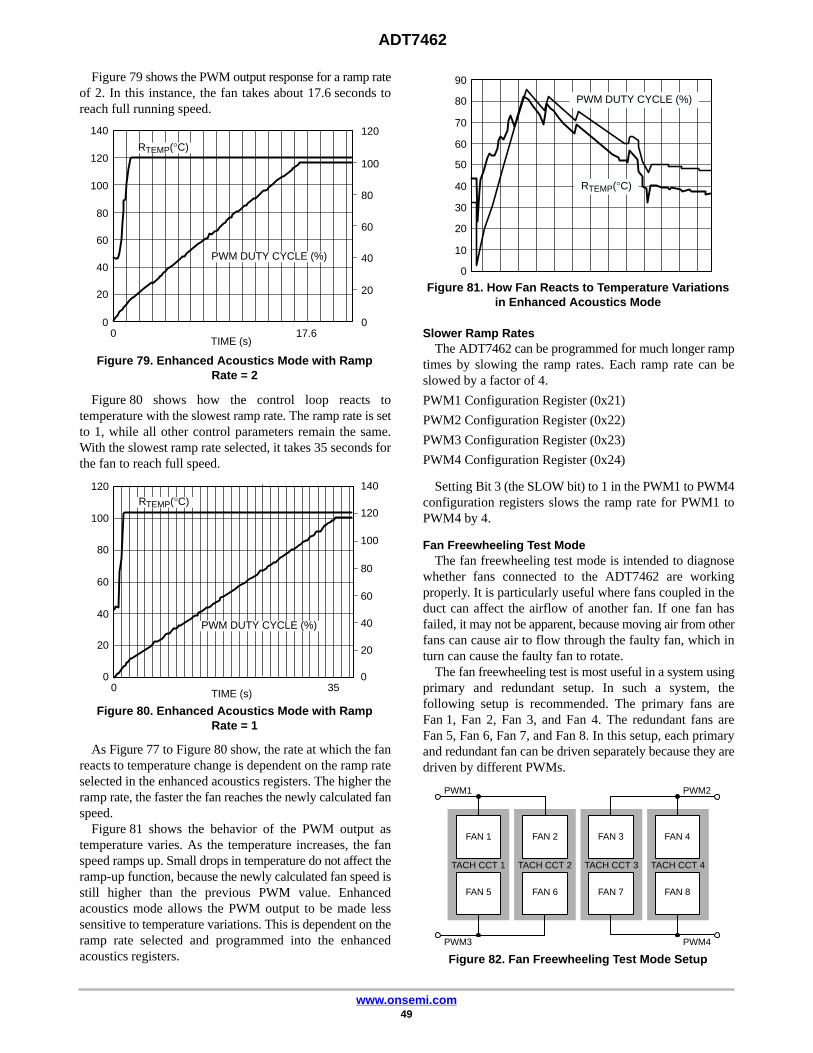
ADT7462
www.onsemi.com49
Figure 79 shows the PWM output response for a ramp rateof 2. In this instance, the fan takes about 17.6 seconds toreach full running speed.
Figure 79. Enhanced Acoustics Mode with RampRate = 2
TIME (s)0
017.6
20
40
60
80
100
120
140
0
20
40
60
80
100
120
RTEMP(°C)
PWM DUTY CYCLE (%)
Figure 80 shows how the control loop reacts totemperature with the slowest ramp rate. The ramp rate is setto 1, while all other control parameters remain the same.With the slowest ramp rate selected, it takes 35 seconds forthe fan to reach full speed.
Figure 80. Enhanced Acoustics Mode with RampRate = 1
TIME (s)00
35
RTEMP(°C)
PWM DUTY CYCLE (%)
0
20
40
60
80
100
120
20
40
60
80
100
120
140
As Figure 77 to Figure 80 show, the rate at which the fanreacts to temperature change is dependent on the ramp rateselected in the enhanced acoustics registers. The higher theramp rate, the faster the fan reaches the newly calculated fanspeed.
Figure 81 shows the behavior of the PWM output astemperature varies. As the temperature increases, the fanspeed ramps up. Small drops in temperature do not affect theramp-up function, because the newly calculated fan speed isstill higher than the previous PWM value. Enhancedacoustics mode allows the PWM output to be made lesssensitive to temperature variations. This is dependent on theramp rate selected and programmed into the enhancedacoustics registers.
Figure 81. How Fan Reacts to Temperature Variationsin Enhanced Acoustics Mode
0
10
20
30
40
50
60
70
80
90
RTEMP(°C)
PWM DUTY CYCLE (%)
Slower Ramp RatesThe ADT7462 can be programmed for much longer ramp
times by slowing the ramp rates. Each ramp rate can beslowed by a factor of 4.
PWM1 Configuration Register (0x21)
PWM2 Configuration Register (0x22)
PWM3 Configuration Register (0x23)
PWM4 Configuration Register (0x24)
Setting Bit 3 (the SLOW bit) to 1 in the PWM1 to PWM4configuration registers slows the ramp rate for PWM1 toPWM4 by 4.
Fan Freewheeling Test ModeThe fan freewheeling test mode is intended to diagnose
whether fans connected to the ADT7462 are workingproperly. It is particularly useful where fans coupled in theduct can affect the airflow of another fan. If one fan hasfailed, it may not be apparent, because moving air from otherfans can cause air to flow through the faulty fan, which inturn can cause the faulty fan to rotate.
The fan freewheeling test is most useful in a system usingprimary and redundant setup. In such a system, thefollowing setup is recommended. The primary fans areFan 1, Fan 2, Fan 3, and Fan 4. The redundant fans areFan 5, Fan 6, Fan 7, and Fan 8. In this setup, each primaryand redundant fan can be driven separately because they aredriven by different PWMs.
Figure 82. Fan Freewheeling Test Mode Setup
FAN 1
PWM2PWM1
FAN 2 FAN 3 FAN 4
TACH CCT 1 TACH CCT 2 TACH CCT 3 TACH CCT 4
FAN 5 FAN 6 FAN 7 FAN 8
PWM4PWM3

ADT7462
www.onsemi.com50
The freewheeling test procedure is as follows:1. PWM1 and PWM2 go to full speed, and PWM3
and PWM4 are switched off.2. After the spin-up time of PWM1 and PWM2 has
elapsed, the speed of Fan 1, Fan 2, Fan 3, andFan 4 is measured.
3. After the speed of Fan 1 and Fan 2 is measured,PWM1 is switched off and PWM3 is spun up.After the spin-up time for PWM3 has elapsed, thespeed of Fan 5 and Fan 6 is measured.
4. After the speed of Fan 3 and Fan 4 is measured,PWM2 is switched off and PWM4 is switched on.After the spin-up time of PWM4 has elapsed, thespeed of Fan 7 and Fan 8 is measured.
5. After the speed of all eight fans has beenmeasured, the TACH and PWM configurationsreturn to their previous values.
• Fans must be in continuous mode for thefreewheeling test; that is, the dc bits must be set(Register 0x08).
• To enable the freewheeling test, set thefreewheeling test enable register (0x1E) to anonzero value. Set Bit 0 = 1 to enable thefreewheeling test for Fan 1, and set Bit 1 for Fan 2,all the way to Bit 7 for Fan 8. The freewheelingtest enable register should be programmed after thefans present register is programmed. If the fanspresent register is not programmed first, then thevalues in the two registers do not match, and theADT7462 assumes that a fan is missing.
The following registers must be programmed for the fanfreewheeling test:
Fans Present Register (0x1D)Set Bit 0 to 1 when a fan is connected to TACH1.Set Bit 1 to 1 when a fan is connected to TACH2.Set Bit 2 to 1 when a fan is connected to TACH3.Set Bit 3 to 1 when a fan is connected to TACH4.Set Bit 4 to 1 when a fan is connected to TACH5.Set Bit 5 to 1 when a fan is connected to TACH6.Set Bit 6 to 1 when a fan is connected to TACH7.Set Bit 7 to 1 when a fan is connected to TACH8.
Fan Freewheeling Test Enable Register (0x1E)Set Bit 0 to 1 to enable the freewheeling test for Fan 1.Set Bit 1 to 1 to enable the freewheeling test for Fan 2.Set Bit 2 to 1 to enable the freewheeling test for Fan 3.Set Bit 3 to 1 to enable the freewheeling test for Fan 4.Set Bit 4 to 1 to enable the freewheeling test for Fan 5.Set Bit 5 to 1 to enable the freewheeling test for Fan 6.Set Bit 6 to 1 to enable the freewheeling test for Fan 7.Set Bit 7 to 1 to enable the freewheeling test for Fan 8.
Fan Freewheeling Test Register (0x1C)Both the Fans Present register (0x1D) and the
freewheeling test enable register (0x1E) should beprogrammed before setting the relevant bits in the fanfreewheeling test register (0x1C). The host fan status
register (0xBD) should be read directly after completion ofthe test.
THERM I/O OperationThis section describes the operation of THERM1 and
THERM2. Pin 28 and Pin 29 can both be configured asTHERM inputs or outputs.
THERM OutputTHERM is not enabled as an output by default on powerup,
but it can be enabled by setting the appropriate bits inRegister 0x0E (THERM1 configuration register) andRegister 0x0F (THERM2 configuration register). THERM1and THERM2 can be configured to assert whenever aspecific channel exceeds the specified THERM limit (seeTable 30).
Table 30. THERM OUTPUT CHANNEL SELECT ANDLIMITS
ChannelEnable
Configuration Limit Registers
THERM1,Register
0x0E
THERM2,Register
0x0F THERM1 THERM2
Local Bit 1 = 1 Bit 1 = 1 0x4C 0x50
Remote 1 Bit 2 = 1 Bit 2 = 1 0x4D 0x51
Remote 2 Bit 3 = 1 Bit 3 = 1 0x4E 0x52
Remote 3 Bit 4 = 1 Bit 4 = 1 0x4F 0x53
As an output, THERM is asserted low to signal that themeasured THERM temperature has exceeded pre-programmed THERM temperature limits. The output isautomatically pulled high again when the temperature fallsbelow the (THERM − Hysteresis) limit. The value ofhysteresis for each channel is programmable in Register0x54 and Register 0x55, where 1 LSB = 1°C, and themaximum hysteresis for each channel is 15°C.
Setting the THERM boost bits, Bit 0 and Bit 1, to Logic 0(default setting) in the THERM configuration register(0x0D), sets the fans to full speed on an internal THERMevent.
THERM InputTo configure THERM as an input, the
THERM1_Timer_Enable (T1TE) bit (Bit 0) in theTHERM1 configuration register (0x0E) and theTHERM2_Timer_Enable (T2TE) bit (Bit 0) in theTHERM2 configuration register (0x0F) must be set toLogic 1. The ADT7462 can then be used to detect when theTHERM pins are asserted low. The THERM pins can beconnected to a trip point temperature sensor or to thePROCHOT output of a CPU.
With processor core voltages reducing all the time, thethreshold for the AGTL + PROCHOT output is also reducedas new processors become available.
Because the THERM input is typically an AGTL + input,the thresholds can be referenced to VCCP. By setting Bit 4 ofConfiguration Register 3 (0x03) to 1, the THERM threshold

ADT7462
www.onsemi.com51
is 2/3 × VCCP, the correct threshold for an AGTL + signal.The THERM assert bits in Host Thermal Status Register 2(0xB9) are set to Logic 1 whenever the THERM input isasserted low. The THERM state bits in Host Thermal StatusRegister 2 (0xB9) indicate that a high-to-low transition hastaken place on the THERM pin.
Figure 83. THERM Behavior
100�C
90�C
80�C
70�C
60�C
50�C
40�C
TEMPERATURE
HIGH TEMP LIMIT
1
32
4
RESET BY MASTER
THERM
ALERT
THERM LIMIT
THERM LIMIT
HYSTERESIS
THERM TimerThe ADT7462 can also measure assertion times on the
THERM inputs as a percentage of a timer window. The timerwindow for the THERM1 input is programmed usingBits [4:2] of the THERM configuration register (0x0D). Thetimer window for the THERM2 input is programmed usingBits [7:5] of the THERM configuration register (0x0D).Values from 0.25 sec to 8 sec are programmable (seeTable 31).
Table 31. THERM TIMER WINDOW
Code THERM Timer Window
000 0.25 sec
001 0.5 sec
010 1 sec
011 2 sec
100 4 sec
101 8 sec
110 8 sec
111 8 sec
The assertion time as a percentage of the timer window isstored in the THERM % on-time registers. This is acumulative sum of the percentage of time during theTHERM timer window that THERM is asserted. The %on-time and associated timer limit registers are listed inTable 32.
Table 32. THERM ON-TIME AND TIMER LIMITREGISTER
Channel % On-Time Register % Timer Limit Register
THERM1 0xAE 0x80
THERM2 0xAF 0x81
When the measured percentage exceeds thecorresponding percentage limit, the T1% bit in HostThermal Status Register 2 (0xB9) is asserted, and anALERT is generated (that is, if the mask bit is not set). If thelimit is set to 0x00, an ALERT is generated on the firstassertion. If the limit is set to 0xFF, an ALERT is nevergenerated because 0xFF corresponds to the THERM inputbeing asserted all the time.
When THERM is configured as an input only, setting Bits[4:1] of the THERM zone in the THERM1 configurationregister (0x0E) and the THERM2 configuration register(0x0F) allows Pin 28/Pin 29 to operate as an I/O.
THERM Timer Limit RegisterThe THERM timer limit is programmed to Register 0x80
and Register 0x81. If THERM is asserted for longer than theprogrammed percentage limit, then an ALERT is generated.The limit is programmed as a percentage of the chosenTHERM timer window.
EXAMPLE: The THERM timer window is eight seconds,and an ALERT should be generated if THERM is assertedfor more than one second.
%Limit � 18� 100 � 12.5%
The THERM timer limit register is an 8−bit register.
0 � 00 � 0%; 0 � FF � 100%
Therefore, 1 LSB = 0.39%
12.5%0.39%
� 32 decimal � 0 � 20 � 00100000
When the time window has elapsed, if the THERM limithas been exceeded, then an ALERT is generated.
General-Purpose I/O PinsThe ADT7462 has eight open-drain GPIO pins. GPIO1 to
GPIO4 can be configured to enable event driven outputs(EDOs), and GPIO5 and GPIO6 can act as EDOs, if the EDOfunctionality is enabled. Two other GPIOs (GPIO7 andGPIO8) are standard GPIO pins that are dedicated togeneral-purpose logic input/output.
Each GPIO pin has five data bits associated with it: threebits in a GPIO configuration register (0x09 and 0x0A), onein the GPIO status register (0xBF), and one in the GPIOmask register (0x36).
Setting a direction bit to 1 in a GPIO configuration registermakes the corresponding GPIO pin an output.
Clearing the direction bit to 0 makes the correspondingGPIO pin an input.
Setting a polarity bit to 1 in a GPIO configuration registermakes the corresponding GPIO pin active high.
Clearing the polarity bit to 0 makes the correspondingGPIO pin active low.
When a GPIO pin is configured as an input, thecorresponding bit in the GPIO status register is read-only,and it is set when the input is asserted (“asserted” can be highor low, depending on the setting of the polarity bit).

ADT7462
www.onsemi.com52
When a GPIO pin is configured as an output, thecorresponding bit in the GPIO status register becomesread/write. Setting this bit then asserts the GPIO output.(Again, “asserted” can be high or low, depending on thesetting of the polarity bit.) The effect of a GPIO statusregister bit on the ALERT output can be masked by settingthe corresponding bit in one of the GPIO mask registers.
When the pin is configured as an output, thecorresponding status bit is automatically masked to preventthe data written to the status bit from causing an interrupt.When configured as inputs, the GPIO pins can be connectedto external interrupt sources such as temperature sensorswith digital output.
EDO CircuitryThe ADT7462 has the added functionality that the
assertion of one of the four GPIOs (GPIO1 to GPIO4) canbe used to latch one of the two EDOs high or low. TheADT7462 has two EDO event mask registers (0x37 and0x38): one mask for each EDO. See Table 33 for anexplanation of event mask register functionality.
The polarity of the EDOs is set in the GPIO configurationregisters (0x09 and 0x0A).
Setting a polarity bit to 1 in one of the GPIO configurationregisters makes the corresponding GPIO pin active high.
Clearing the polarity bit to 0 makes it active low.
Figure 84. EDO Circuit
GPIO1
GPIO2GPIO3GPIO4
EDO (GPIO5)
EDO (GPIO6)LATCHEVENTMASK
Bits [7:5] of each event mask register (0x37 and 0x38)allow the EDO output to be driven high or low (dependingon the polarity bit of the configuration register) and latched(depending on the EDO latch bit of the configurationregister), if the ADT7462 detects an overtemperature, anover/undervoltage, or a fan failure condition.
Table 33. EDO CONTROL (MASK) REGISTER 0X37 AND REGISTER 0X38
Bit 7:Overvoltage/Undervoltage Bit 6: THERM Bit 5: Fan Fail Bit 3 Bit 2 Bit 1 Bit 0
Behavior: What Drives andLatches Output X (G = GPIO)
0 = Drive Output X 0 = Drive Output X 0 = Drive Output X 0 0 0 0 G4 or G3 or G2 or G1
1 = Ignore Event 1 = Ignore Event 1 = Ignore Event 0 0 0 1 G4 or G3 or G2
0 0 1 0 G4 or G3 or G1
0 0 1 1 G4 or G3
0 1 0 0 G4 or G2 or G1
0 1 0 1 G4 or G2
0 1 1 0 G4 or G1
0 1 1 1 G4
1 0 0 0 G3 or G2 or G1
1 0 0 1 G3 or G2
1 0 1 0 G3 or G1
1 0 1 1 G3
1 1 0 0 G2 or G1
1 1 0 1 G2
1 1 1 0 G1
1 1 1 1 GPIO Events Ignored by Output X
Table 33 shows that any of the four designated GPIO pinscan be used to set or reset either one of the two EDO outputs.
Using this functionality, it is possible to have theADT7462 drive LEDs or signals based on rules. Forexample, if a GPIO1 (power fail), a GPIO2 (overcurrent), oran overtemperature condition occurs, EDO1 (power supplyfault LED) can be latched. This does not require softwarehandling and makes the part more autonomous.
Other Digital InputsThe ADT7462 contains other specific digital inputs that
can be found on PC motherboards. These inputs can bemonitored and configured for actions to occur on theirassertion.
ADT7462
www.onsemi.com53
VR_HOT InputsPin 25 and Pin 26 can be configured as VR_HOT inputs.
These are specific digital signals from the CPU voltageregulator that indicate an overtemperature. On assertion ofthese inputs, the relevant status bits are set in Thermal StatusRegister 2 (Host Register 0xB9 or BMC Register 0xC1).Assertion of these inputs can also be used to boost the fansto full speed, thus providing emergency cooling in the eventof VR overtemperature. This is set using Bit 3 (VRD1) andBit 4 (VRD2) of Configuration Register 2 (0x02). There isalso an associated mask bit in Register 0x31 to mask theassertion of these inputs from the ALERT output.
SCSI_TERM InputsPin 16 and Pin 20 can be configured as SCSI_TERM
inputs. An assertion on the SCSI_TERM is recorded in Bit 4and Bit 5 of Host Digital Status Register (0xBE) or BMCDigital Status Register (0xC6). There is also an associatedmask bit in Register 0x35 to mask the assertion of theseinputs from the ALERT output.
Reset I/OThe ADT7462 includes an active low reset pin (Pin 14).
The RESET pin can be both a reset input and output. RESETmonitors the VCC input to the ADT7462. At powerup,RESET is asserted (pulled low) until 180 ms after the powersupply has risen above the supply threshold. A power-onreset initializes all registers to the default values.
Figure 85. Operation of RESET Output on Powerup
VCC1.0 V
180 ms
RESET
The RESET pin can also function as a reset input. Pullingthis pin low externally resets the ADT7462. The user shouldwait at least 180 ms after powerup before doing a hardwarereset. The reset pulse width should be greater than 0.8 ms toensure that a reset is registered.
A hardware reset differs from a power-on reset in that notall of the registers are reinitialized to the default values. Forexample, limit registers are not all restored to the defaultvalues. This can be useful if the user needs to reset the partbut does not want to completely reprogram the device. TheRegister Map section show, which registers, are reset.Locked registers are not restored to default values by ahardware reset.
Note that if two ADT7462 devices are used in one system,the RESET pins should not be connected together betweendevices. Doing so causes one device to reset the other on apower-on reset.
Software ResetThe ADT7462 can be reset in software by setting Bit 7 of
Configuration Register 0 (0x00). The code 0x6D must bewritten to Register 0x7B before setting the software reset bit.This register is cleared to the power-on default after thesoftware reset.
Note that not all registers are restored to their defaultvalues on a reset. The same registers are reset by a hardwareand software reset. The Register Map section provides acomplete reference of registers that are reset.
Chassis Intrusion InputThe chassis intrusion (CI) input is an active high input
intended for detection and signaling of unauthorizedtampering with the system. When this input goes high, theevent is latched in Bit 7 of Host Digital Status Register(0xBE), and an interrupt is generated. The bit remains setuntil cleared by writing a 1 to CI reset (CI_R), Bit 5 ofConfiguration Register 3 (0x03). The CI reset bit is clearedby writing a 0 to it.
The CI circuit is powered from the VBATT voltagechannel. Pin 26 must be configured to monitor VBATT anda battery must be connected to monitor CI events. CImonitoring is disabled if the measured VBATT value (0x93)is less than the lower voltage limit (0x75) of Pin 26.
The CI input detects chassis intrusion events even whenthe ADT7462 is powered off (provided battery voltage isapplied to VBATT) but does not immediately generate aninterrupt. When a chassis intrusion event is detected andlatched, an interrupt is generated when the system ispowered on.
The actual detection of chassis intrusion is performed byan external circuit that detects, for example, when the coverhas been removed. A wide variety of techniques can be usedfor chassis detection. For example,• A microswitch that opens or closes when the cover is
removed• A reed switch operated by a magnet affixed to the cover
• A hall-effect switch operated by a magnet affixed to thecover
• A photo-transistor that detects light when the cover isremoved
Powerup SequenceThe powerup sequence of the ADT7462 is as follows:
1. The temperature of the thermal diode connected toPin 17 and Pin 18 (only dedicated thermal diodechannel) is monitored immediately on powerup ofthe ADT7462. Ideally, the hottest zone should beconnected to this channel so protection is providedimmediately on powerup.
2. VCCP1 is also monitored immediately on powerup.VCCP1 is typically connected to a main power rail.
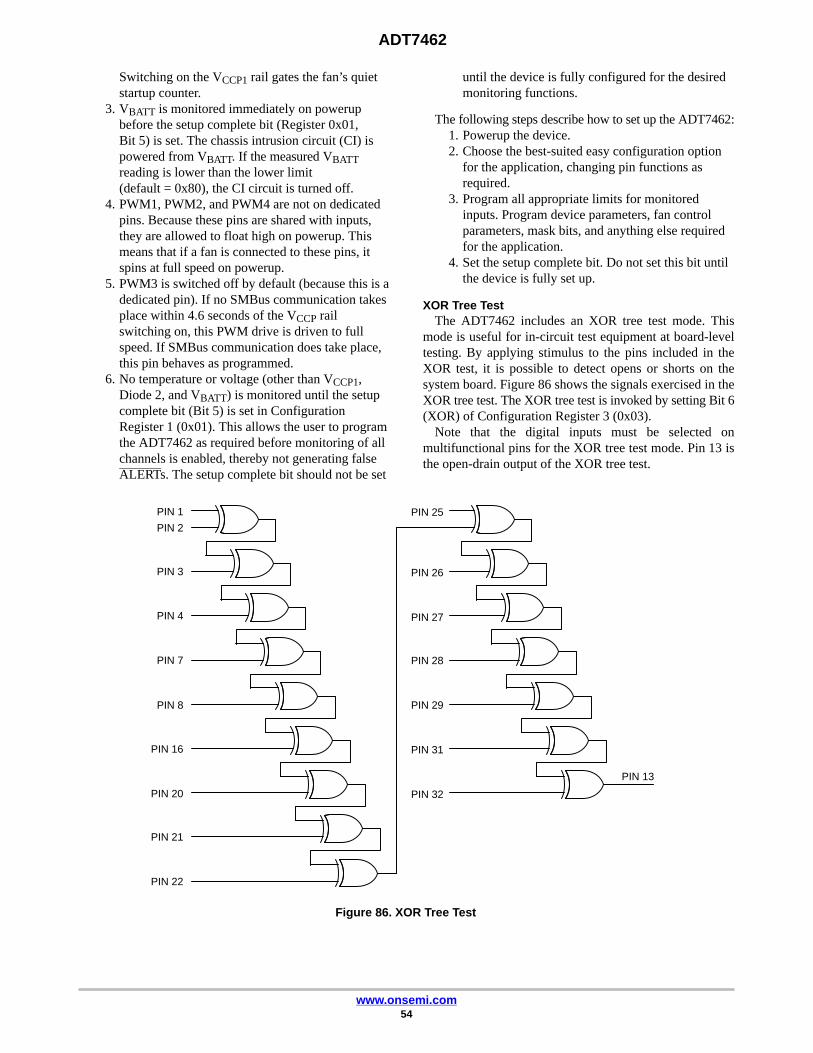
ADT7462
www.onsemi.com54
Switching on the VCCP1 rail gates the fan’s quietstartup counter.
3. VBATT is monitored immediately on powerupbefore the setup complete bit (Register 0x01,Bit 5) is set. The chassis intrusion circuit (CI) ispowered from VBATT. If the measured VBATTreading is lower than the lower limit(default = 0x80), the CI circuit is turned off.
4. PWM1, PWM2, and PWM4 are not on dedicatedpins. Because these pins are shared with inputs,they are allowed to float high on powerup. Thismeans that if a fan is connected to these pins, itspins at full speed on powerup.
5. PWM3 is switched off by default (because this is adedicated pin). If no SMBus communication takesplace within 4.6 seconds of the VCCP railswitching on, this PWM drive is driven to fullspeed. If SMBus communication does take place,this pin behaves as programmed.
6. No temperature or voltage (other than VCCP1,Diode 2, and VBATT) is monitored until the setupcomplete bit (Bit 5) is set in ConfigurationRegister 1 (0x01). This allows the user to programthe ADT7462 as required before monitoring of allchannels is enabled, thereby not generating falseALERTs. The setup complete bit should not be set
until the device is fully configured for the desiredmonitoring functions.
The following steps describe how to set up the ADT7462:1. Powerup the device.2. Choose the best-suited easy configuration option
for the application, changing pin functions asrequired.
3. Program all appropriate limits for monitoredinputs. Program device parameters, fan controlparameters, mask bits, and anything else requiredfor the application.
4. Set the setup complete bit. Do not set this bit untilthe device is fully set up.
XOR Tree TestThe ADT7462 includes an XOR tree test mode. This
mode is useful for in-circuit test equipment at board-leveltesting. By applying stimulus to the pins included in theXOR test, it is possible to detect opens or shorts on thesystem board. Figure 86 shows the signals exercised in theXOR tree test. The XOR tree test is invoked by setting Bit 6(XOR) of Configuration Register 3 (0x03).
Note that the digital inputs must be selected onmultifunctional pins for the XOR tree test mode. Pin 13 isthe open-drain output of the XOR tree test.
Figure 86. XOR Tree Test
PIN 1
PIN 13
PIN 2
PIN 3
PIN 4
PIN 7
PIN 8
PIN 16
PIN 20
PIN 21
PIN 22
PIN 32
PIN 31
PIN 29
PIN 28
PIN 27
PIN 26
PIN 25

ADT7462
www.onsemi.com55
Register Tables
Table 34. REGISTER MAP
Addr Description R/W Bit 7 Bit 6 Bit 5 Bit 4 Bit 3 Bit 2 Bit 1 Bit 0De-fault
SWReset
Lockable
0x00 Config 0 R/W SW Reset VID # Bytes # Bytes #Bytes # Bytes # Bytes # Bytes 0x20 Yes Yes
0x01 Config 1 R/W RDY Lock SC DFS ALERT Res Res Mon 0x81 Yes Yes
0x02 Config 2 R/W #FP #FP FMS VRD2 VRD1 PWM Res FAST 0x80 Yes Yes
0x03 Config 3 R/W V_Core_Low
XOR CI_R TT VID_T SDA SCL GPIO 0x00 Yes Yes
0x07 TACH Enable
R/W T8E T7E T6E T5E T4E T3E T2E T1E 0x00 Yes Yes
0x08 TACH Config
R/W Res Res Res Res DC 4/8 DC 3/7 DC 2/6 DC 1/5 0x0F Yes Yes
0x09 GPIO1_Bhvr
R/W D4 P4 D3 P3 D2 P2 D1 P1 0x00 Yes Yes
0x0A GPIO2_Bhvr
R/W D8 P8 D7 P7 D6 P6 D5 P5 0x00 Yes Yes
0x0B TMIN_Cal1 R/W Res Res P2R2 P2R1 P1R2 P1R1 R2 R1 0x00 Yes Yes
0x0C TMIN_Cal2 R/W Res CtrlLoopSelect
CYR2 CYR2 CYR2 CYR1 CYR1 CYR1 0x40 Yes Yes
0x0D THERMConf
R/W TW2 TW2 TW2 TW1 TW1 TW1 B2 B1 0x00 Yes Yes
0x0E Conf_THERM1
R/W Res Res Res R3 R2 R1 Local T1TE 0x00 Yes Yes
0x0F Conf_THERM2
R/W Res Res Res R3 R2 R1 Local T2TE 0x00 Yes Yes
0x10 Pin Conf 1 R/W VID D1 D3 Pin 1 Pin 2 Pin 3 Pin 4 Pin 7 0x7F Yes Yes
0x11 Pin Conf 2 R/W Pin 8 Pin 13 Pin 15 Pin 19 Pin 21 Pin 22 Pin 23 Pin 23 0xCE Yes Yes
0x12 Pin Conf 3 R/W Pin 24 Pin 24 Pin 25 Pin 25 Pin 26 Pin 26 Pin 27 Res 0x42 Yes Yes
0x13 Pin Conf 4 R/W Pin 28 Pin 28 Pin 29 Pin 29 Pin 31 Pin 32 Res Res 0xFC Yes Yes
0x14 Easy Conf R/W Res Res Res Op5 Op4 Op3 Op2 Op1 0x01 Yes Yes
0x16 EDO Enable
R/W CS CS CS CS CS SC EDO2 EDO1 0x00 Yes Yes
0x18 Attenuators1 En
R/W Pin 22 Pin 21 Pin 19 Pin 15 Pin 13 Pin 8 Pin 7 Res 0xFF Yes Yes
0x19 Attenuators2 En
R/W Res Res Pin 29 Pin 28 Res Pin 25 Pin 24 Pin 23 0x37 Yes Yes
0x1A EnhancedAcoustics 1
R/W RR2 RR2 RR2 RR1 RR1 RR1 En2 En1 0x00 Yes Yes
0x1B EnhancedAcoustics 2
R/W RR4 RR4 RR4 RR3 RR3 RR3 En4 En3 0x00 Yes Yes
0x1C Fan Free-wheel Test
R/W Fan 8 Fan 7 Fan 6 Fan 5 Fan 4 Fan 3 Fan 2 Fan 1 0x00 Yes Yes
0x1D FansPresent
R/W F8P F7P F6P F5P F4P F3P F2P F1P 0x00 Yes Yes
0x1E Fan Free-wheelTestEn
R/W Fan 8 Fan 7 Fan 6 Fan 5 Fan 4 Fan 3 Fan 2 Fan 1 0x00 Yes Yes
0x21 PWM1Config
R/W BHVR BHVR BHVR INV SLOW Spin Spin Spin 0x11 Yes Yes
0x22 PWM2Config
R/W BHVR BHVR BHVR INV SLOW Spin Spin Spin 0x31 Yes Yes
0x23 PWM3Config
R/W BHVR BHVR BHVR INV SLOW Spin Spin Spin 0x51 Yes Yes
0x24 PWM4Config
R/W BHVR BHVR BHVR INV SLOW Spin Spin Spin 0x71 Yes Yes
0x25 PWM1,PWM2Freq
R/W F2 F2 F2 F1 F1 F1 Min 2 Min 1 0x90 Yes Yes
0x26 PWM3,PWM4Freq
R/W F4 F4 F4 F3 F3 F3 Min 4 Min 3 0x90 Yes Yes

ADT7462
www.onsemi.com56
Table 34. REGISTER MAP
AddrLockable
SWReset
De-faultBit 0Bit 1Bit 2Bit 3Bit 4Bit 5Bit 6Bit 7R/WDescription
0x28 PWM1 Min R/W 7 6 5 4 3 2 1 0 0x80 Yes Yes
0x29 PWM2 Min R/W 7 6 5 4 3 2 1 0 0x80 Yes Yes
0x2A PWM3 Min R/W 7 6 5 4 3 2 1 0 0x80 Yes Yes
0x2B PWM4 Min R/W 7 6 5 4 3 2 1 0 0x80 Yes Yes
0x2C PWM1 toPWM4 Max
R/W 7 6 5 4 3 2 1 0 0xC0 Yes Yes
0x30 ThermalMask 1
R/W R3D R2D R1D R3 R2 R1 Local Res 0x00 Yes No
0x31 ThermalMask 2
R/W VRD2 VRD1 T2S T2A T2% T1S T1A T1% 0xC0 Yes No
0x32 VoltageMask 1
R/W P23 +5V P19 P15 +3.3V +12V3 +12V2 +12V1 0x00 Yes No
0x33 VoltageMask 2
R/W +1.5V1(ICH)
+1.5V2(3GIO)
P26 P25 P24 Res Res Res 0x00 Yes No
0x34 Fan Mask R/W Fan 8 Fan 7 Fan 6 Fan 5 Fan 4 Fan 3 Fan 2 Fan 1 0x00 Yes No
0x35 DigitalMask
R/W CI VID SCSI2 SCSI1 FAN2MAX Res Res Res 0x38 Yes No
0x36 GPIO Mask R/W GPIO8 GPIO7 GPIO6 GPIO5 GPIO4 GPIO3 GPIO2 GPIO1 0x00 Yes No
0x37 EDO Mask1
R/W Volt Temp Fan Res GPIO4 GPIO3 GPIO2 GPIO1 0x00 Yes No
0x38 EDO Mask2
R/W Volt Temp Fan Res GPIO4 GPIO3 GPIO2 GPIO1 0x00 Yes No
0x3D Device ID R 7 6 5 4 3 2 1 0 0x62 No N/A
0x3E Comp ID R 7 6 5 4 3 2 1 0 0x41 No N/A
0x3F Rev No R 7 6 5 4 3 2 1 0 0x04 No N/A
0x44 Local LowTemp Limit
R/W 7 6 5 4 3 2 1 0 0x40 No No
0x45 Remote1/Pin 15Low TempLimit
R/W 7 6 5 4 3 2 1 0 0x40 No No
0x46 Remote 2Low TempLimit
R/W 7 6 5 4 3 2 1 0 0x40 No No
0x47 Remote3/Pin 19Low TempLimit
R/W 7 6 5 4 3 2 1 0 0x40 No No
0x48 Local HighLimit
R/W 7 6 5 4 3 2 1 0 0x95 No No
0x49 Remote1/Pin 15High Limit
R/W 7 6 5 4 3 2 1 0 0x95 No No
0x4A Remote 2High Limit
R/W 7 6 5 4 3 2 1 0 0x95 No No
0x4B Remote3/Pin 19High Limit
R/W 7 6 5 4 3 2 1 0 0x95 No No
0x4C LocalTHERM1/+1.5V2(3GIO)High
R/W 7 6 5 4 3 2 1 0 0xA4 No Yes
0x4D Remote 1THERM1Limit
R/W 7 6 5 4 3 2 1 0 0xA4 No Yes
0x4E Remote 2THERM1Limit
R/W 7 6 5 4 3 2 1 0 0xA4 No Yes
0x4F Remote 3THERM1Limit
R/W 7 6 5 4 3 2 1 0 0xA4 No Yes

ADT7462
www.onsemi.com57
Table 34. REGISTER MAP
AddrLockable
SWReset
De-faultBit 0Bit 1Bit 2Bit 3Bit 4Bit 5Bit 6Bit 7R/WDescription
0x50 LocalTHERM2/+1.5V1(ICH) High
R/W 7 6 5 4 3 2 1 0 0xA4 No Yes
0x51 Remote 1THERM2Limit
R/W 7 6 5 4 3 2 1 0 0xA4 No Yes
0x52 Remote 2THERM2Limit
R/W 7 6 5 4 3 2 1 0 0xA4 No Yes
0x53 Remote 3THERM2Limit
R/W 7 6 5 4 3 2 1 0 0xA4 No Yes
0x54 Local/Re-mote1Temp Hyst
R/W LH LH LH LH R1H R1H R1H R1H 0x44 No Yes
0x55 Remote 2/Remote 3Temp Hyst
R/W R2H R2H R2H R2H R3H R3H R3H R3H 0x44 No Yes
0x56 Local Offset R/W 7 6 5 4 3 2 1 0 0x00 No Yes
0x57 Remote 1 Offset
R/W 7 6 5 4 3 2 1 0 0x00 No Yes
0x58 Remote 2 Offset
R/W 7 6 5 4 3 2 1 0 0x00 No Yes
0x59 Remote 3 Offset
R/W 7 6 5 4 3 2 1 0 0x00 No Yes
0x5A Remote 1OperatingPoint
R/W 7 6 5 4 3 2 1 0 0xA4 Yes Yes
0x5B Remote 2OperatingPoint
R/W 7 6 5 4 3 2 1 0 0xA4 Yes Yes
0x5C Local TempTMIN
R/W 7 6 5 4 3 2 1 0 0x9A Yes Yes
0x5D Remote 1Temp TMIN
R/W 7 6 5 4 3 2 1 0 0x9A Yes Yes
0x5E Remote 2Temp TMIN
R/W 7 6 5 4 3 2 1 0 0x9A Yes Yes
0x5F Remote 3Temp TMIN
R/W 7 6 5 4 3 2 1 0 0x9A Yes Yes
0x60 LocalTRANGE/Hyst
R/W Range Range Range Range Hys Hys Hys Hys 0xC4 Yes Yes
0x61 Remote 1TRANGE/Hyst
R/W Range Range Range Range Hys Hys Hys Hys 0xC4 Yes Yes
0x62 Remote 2TRANGE/Hyst
R/W Range Range Range Range Hys Hys Hys Hys 0xC4 Yes Yes
0x63 Remote 3TRANGE/Hyst
R/W Range Range Range Range Hys Hys Hys Hys 0xC4 Yes Yes
0x64 OperatingPoint Hyst
R/W Hys Hys Hys Hys Res Res Res Res 0x40 Yes Yes
0x68 +3.3V High Limit
R/W 7 6 5 4 3 2 1 0 0xFF No No
0x69 Pin 23VoltageHigh Limit
R/W 7 6 5 4 3 2 1 0 0xFF No No
0x6A Pin 24VoltageHigh Limit
R/W 7 6 5 4 3 2 1 0 0xFF No No
0x6B Pin 25VoltageHigh Limit
R/W 7 6 5 4 3 2 1 0 0xFF No No

ADT7462
www.onsemi.com58
Table 34. REGISTER MAP
AddrLockable
SWReset
De-faultBit 0Bit 1Bit 2Bit 3Bit 4Bit 5Bit 6Bit 7R/WDescription
0x6C Pin 26VoltageHigh Limit
R/W 7 6 5 4 3 2 1 0 0xFF No No
0x6D +12V1 Low Limit
R/W 7 6 5 4 3 2 1 0 0x00 No No
0x6E +12V2 Low Limit
R/W 7 6 5 4 3 2 1 0 0x00 No No
0x6F +12V3 Low Limit
R/W 7 6 5 4 3 2 1 0 0x00 No No
0x70 +3.3V LowLimit
R/W 7 6 5 4 3 2 1 0 0x00 No No
0x71 +5V LowLimit
R/W 7 6 5 4 3 2 1 0 0x00 No No
0x72 Pin 23VoltageLow Limit
R/W 7 6 5 4 3 2 1 0 0x20 No No
0x73 Pin 24VoltageLow Limit
R/W 7 6 5 4 3 2 1 0 0x00 No No
0x74 Pin 25VoltageLow Limit
R/W 7 6 5 4 3 2 1 0 0x00 No No
0x75 Pin 26VoltageLow Limit
R/W 7 6 5 4 3 2 1 0 0x80 No No
0x76 +1.5V2(3GIO) LowLimit
R/W 7 6 5 4 3 2 1 0 0x00 No No
0x77 +1.5V1(ICH) LowLimit
R/W 7 6 5 4 3 2 1 0 0x00 No No
0x78 TACH1Limit/VID
R/W 7 6 5 4 3 2 1 0 0xFF No Yes
0x79 TACH2Limit
R/W 7 6 5 4 3 2 1 0 0xFF No Yes
0x7A TACH3Limit
R/W 7 6 5 4 3 2 1 0 0xFF No Yes
0x7B TACH4Limit
R/W 7 6 5 4 3 2 1 0 0xFF No Yes
0x7C TACH5/+12V1 HighLimit
R/W 7 6 5 4 3 2 1 0 0xFF No Yes
0x7D TACH6/+12V2 HighLimit
R/W 7 6 5 4 3 2 1 0 0xFF No Yes
0x7E TACH7/+5VHigh Limit
R/W 7 6 5 4 3 2 1 0 0xFF No Yes
0x7F TACH8/+12V3 HighLimit
R/W 7 6 5 4 3 2 1 0 0xFF No Yes
0x80 THERM1Timer Limit
R/W 7 6 5 4 3 2 1 0 0xFF No Yes
0x81 THERM2Timer Limit
R/W 7 6 5 4 3 2 1 0 0xFF No Yes
0x88 Local TempValue,LSBs
R 7 6 5 4 3 2 1 0 0x00 No No
0x89 Local TempValue,MSBs
R 7 6 5 4 3 2 1 0 0x00 No No
0x8A Remote 1Temp,LSBs
R 7 6 5 4 3 2 1 0 0x00 No No

ADT7462
www.onsemi.com59
Table 34. REGISTER MAP
AddrLockable
SWReset
De-faultBit 0Bit 1Bit 2Bit 3Bit 4Bit 5Bit 6Bit 7R/WDescription
0x8B Remote 1Temp,MSBs, Pin 15 Volt
R 7 6 5 4 3 2 1 0 0x00 No No
0x8C Remote 2Temp,LSBs
R 7 6 5 4 3 2 1 0 0x00 No No
0x8D Remote 2Temp,MSBs
R 7 6 5 4 3 2 1 0 0x00 No No
0x8E Remote 3Temp,LSBs
R 7 6 5 4 3 2 1 0 0x00 No No
0x8F Remote 3Temp,MSBs, Pin 19 Volt
R 7 6 5 4 3 2 1 0 0x00 No No
0x90 Pin 23Voltage
R 7 6 5 4 3 2 1 0 0x00 No No
0x91 Pin 24Voltage
R 7 6 5 4 3 2 1 0 0x00 No No
0x92 Pin 25Voltage
R 7 6 5 4 3 2 1 0 0x00 No No
0x93 Pin 26Voltage
R 7 6 5 4 3 2 1 0 0x00 No No
0x94 +1.5V1(ICH) Volt
R 7 6 5 4 3 2 1 0 0x00 No No
0x95 +1.5V2(3GIO)Voltage
R 7 6 5 4 3 2 1 0 0x00 No No
0x96 +3.3VVoltage
R 7 6 5 4 3 2 1 0 0x00 No No
0x97 VID Value R 7 6 5 4 3 2 1 0 0x00 No No
0x98 TACH1Value,LSBs
R 7 6 5 4 3 2 1 0 0xFF No No
0x99 TACH1Value,MSBs
R 7 6 5 4 3 2 1 0 0xFF No No
0x9A TACH2Value,LSBs
R 7 6 5 4 3 2 1 0 0xFF No No
0x9B TACH2Value,MSBs
R 7 6 5 4 3 2 1 0 0xFF No No
0x9C TACH3Value,LSBs
R 7 6 5 4 3 2 1 0 0xFF No No
0x9D TACH3Value,MSBs
R 7 6 5 4 3 2 1 0 0xFF No No
0x9E TACH4Value,LSBs
R 7 6 5 4 3 2 1 0 0xFF No No
0x9F TACH4Value,MSBs
R 7 6 5 4 3 2 1 0 0xFF No No
0xA0 Unused R 7 6 5 4 3 2 1 0 N/A No No
0xA1 Unused R 7 6 5 4 3 2 1 0 N/A No No
0xA2 TACH5Value, LSB
R 7 6 5 4 3 2 1 0 0xFF No No
0xA3 TACH5MSB/+12V1V
R 7 6 5 4 3 2 1 0 0xFF No No
0xA4 TACH6Value, LSB
R 7 6 5 4 3 2 1 0 0xFF No No

ADT7462
www.onsemi.com60
Table 34. REGISTER MAP
AddrLockable
SWReset
De-faultBit 0Bit 1Bit 2Bit 3Bit 4Bit 5Bit 6Bit 7R/WDescription
0xA5 TACH6MSB/+12V2 Voltage
R 7 6 5 4 3 2 1 0 0xFF No No
0xA6 TACH7Value, LSB
R 7 6 5 4 3 2 1 0 0xFF No No
0xA7 TACH7MSB/+5VVoltage
R 7 6 5 4 3 2 1 0 0xFF No No
0xA8 TACH8Value, LSB
R 7 6 5 4 3 2 1 0 0xFF No No
0xA9 TACH8MSB/+12V3 Voltage
R 7 6 5 4 3 2 1 0 0xFF No No
0xAA PWM1Duty Cycle
R/W 7 6 5 4 3 2 1 0 0x00 No No
0xAB PWM2Duty Cycle
R/W 7 6 5 4 3 2 1 0 0x00 No No
0xAC PWM3Duty Cycle
R/W 7 6 5 4 3 2 1 0 0xC0 No No
0xAD PWM4Duty Cycle
R/W 7 6 5 4 3 2 1 0 0x00 No No
0xAE THERM1%On−Time
R 7 6 5 4 3 2 1 0 0x00 No No
0xAF THERM2%On−Time
R 7 6 5 4 3 2 1 0 0x00 No No
0xB8 ThermalStatus 1,Host
R R3D R2D R1D R3 R2 R1 Local Res 0x00 Yes No
0xB9 ThermalStatus 2,Host
R VR2 VR1 T2S T2A T2% T1S T1A T1% 0x00 Yes No
0xBA ThermalStatus 3,Host
R R3T2 R2T2 R1T2 LT2 R3T1 R2T1 R1T1 LT1 0x00 Yes No
0xBB VoltageStatus 1,Host
R Pin 23 +5V Pin 19 Pin 15 +3.3V +12V3 +12V2 +12V1 0x00 Yes No
0xBC VoltageStatus 2,Host
R +1.5V1(ICH)
+1.5V2(3GIO)
Pin 26 Pin 25 Pin 24 Res Res Res 0x00 Yes No
0xBD Fan Status,Host
R Fan 8 Fan 7 Fan 6 Fan 5 Fan 4 Fan 3 Fan 2 Fan 1 0x00 Yes No
0xBE DigitalStatus,Host
R CI VID SCSI2 SCSI1 FAN2MAX Res Res Res 0x00 Yes No
0xBF GPIOStatus,Host
R/W GPIO8 GPIO7 GPIO6 GPIO5 GPIO4 GPIO3 GPIO2 GPIO1 0x00 Yes No
0xC0 ThermalStatus 1,BMC
R R3D R2D R1D R3 R2 R1 Local Res 0x00 Yes No
0xC1 ThermalStatus 2,BMC
R VR2 VR1 T2S T2A T2% T1S T1A T1% 0x00 Yes No
0xC3 VoltageStatus 1,BMC
R Pin 23 +5V Pin 19 Pin 15 +3.3V +12V3 +12V2 +12V1 0x00 Yes No
0xC4 VoltageStatus 2,BMC
R +1.5V1(ICH)
+1.5V2(3GIO)
Pin 26 Pin 25 Pin 24 Res Res Res 0x00 Yes No
0xC5 Fan Status,BMC
R Fan 8 Fan 7 Fan 6 Fan 5 Fan 4 Fan 3 Fan 2 Fan 1 0x00 Yes No
0xC6 DigitalStatus,BMC
R CI VID SCSI2 SCSI1 FAN2MAX Res Res Res 0x00 Yes No
ADT7462
www.onsemi.com61
Table 35. REGISTER 0X00 − CONFIGURATION REGISTER 0 (Note 1)
Bit Name R/W Description
[5:0] #Bytes BlockRead
R/W These bits set the number of registers to be read in a block read. Default = 0x20.
6 VID Decoder R/W 0 = VR10 Decoding Spec; 1 = VR11 Decoding Spec. Default = 0.
7 SW Reset R/W Setting this bit to 1 restores all unlocked registers to their default values. Self-clearing. Write0x6D to register 0x7B before setting this bit to get a software reset. Default = 0.
1. POR = 0x20, Lock = Y, SW Reset = Y.
Table 36. REGISTER 0X01 − CONFIGURATION REGISTER 1 (Note 1)
Bit Name R/W Description
0 Monitor R/W Setting this bit to 1 enables temperature and voltage measurements. When this bit is set to 0,temperature and voltage measurements are disabled. Default = 1.
1 Reserved R/W Reserved. Default = 0.
2 Reserved R/W Reserved. Default = 0.
3 ALERT Mode R/W This bit sets the ALERT mode in the ADT7462. 1 = comparator mode, 0 = SMBALERT mode(Default).
4 Disable FastSpin-Up
R/W Setting this bit to 1 disables the fast spin-up (for two TACH pulses) for the fans. Instead, thefans spin up for the programmed fan startup timeout. Default = 0.
5 Setup Complete R/W Setting this bit to 1 tells the ADT7462 that setup is complete and that monitoring of all selectedchannels should begin. Default = 0.
6 Lock WriteOnce
Logic 1 locks all limit values at their current settings. When this bit is set, all lockable registersbecome read-only and cannot be modified until the ADT7462 is powered down and poweredup again. This prevents rogue programs, such as viruses, from modifying critical system limitsettings. Lockable.
7 RDY R This bit is set to 1 to indicate that the ADT7462 is fully powered up and ready to startmonitoring.
1. POR = 0x81, Lock = Y, SW Reset = Y.
Table 37. REGISTER 0X02 − CONFIGURATION REGISTER 2 (Note 1)
Bit Name R/W Description
0 FAST R/W In low frequency, PWM fan speed measurements are made once a second. Setting this bit to 1increases the frequency of the fan speed measurements to 4 times a second. Default = 0.
1 Reserved R/W Reserved. Default = 0.
2 PWM Mode R/W This bit sets the PWM frequency mode. 0 = low frequency PWM; frequency programmablebetween 11 Hz and 88.2 Hz. Default = 35.3 Hz. 1 = high frequency mode, 22.5 kHz.
3 VRD1 Boost R/W Setting this bit to 0 causes the fans to go to full speed on assertion of VRD1. Default = 0.When this bit is set to 1, VRD1 assertions have no effect on the fan speed.
4 VRD2 Boost R/W Setting this bit to 0 causes the fans to go to full speed on assertion of VRD2. Default = 0.When this bit is set to 1, VRD2 assertions have no effect on the fan speed.
5 Fans Full Speed R/W Setting this bit to 1 drives the fans to full speed. Default = 0.
[7:6] #TACH Pulses R/W In low frequency mode, the ADT7462 must pulse stretch to get an accurate fan speedmeasurement. The speed is always measured between the 2nd rising edge and one × TACHpulses later. This bit determines the last TACH pulse. Therefore, if the fan speed is to bemeasured between the second and fourth TACH pulse, 01 is written to these bits.
x = 1 = 00x = 2 = 01x = 3 = 10 (Default)x = 4 = 11
1. POR = 0x80, Lock = Y, SW Reset = Y.
ADT7462
www.onsemi.com62
Table 38. REGISTER 0X03 − CONFIGURATION REGISTER 3 (Note 1)
Bit Name R/W Description
0 GPIO_En R/W Setting this bit to 1 enables the GPIOs. Default = 0.
1 SCL_Timeout R/W 1 = SCL timeout enabled. 0 = SCL timeout disabled = default.
2 SDA_Timeout R/W 1 = SDA timeout enabled. 0 = SDA timeout disabled = default.
3 VID_Threshold R/W This bit sets the digital threshold for the VID digital inputs. 0 = default. 1 = low thresholdsselected = 0.65 V.
4 THERM_Threshold
R/W This bit sets the digital threshold for the THERM digital inputs. 0 = default. 1 = low thresholdsselected = 2/3 VCCP1 (Pin 23).
5 CI Reset R/W Setting this bit to 1 resets the chassis intrusion circuit. This bit clears itself. Default = 0.
6 XOR Tree R/W Setting this bit to 1 enables the XOR tree test. Default = 0.
7 V_Core_Low R/W Setting this bit to 1 enables V_core_low. Default = 0.
1. POR = 0x00, Lock = Y, SW Reset = Y.
Table 39. REGISTER 0X07 − TACH ENABLE REGISTER (Note 1)
Bit Name R/W Description
0 TACH1 R/W Setting this bit to 1 enables the TACH1 measurement. Default = 0.
1 TACH2 R/W Setting this bit to 1 enables the TACH2 measurement. Default = 0.
2 TACH3 R/W Setting this bit to 1 enables the TACH3 measurement. Default = 0.
3 TACH4 R/W Setting this bit to 1 enables the TACH4 measurement. Default = 0.
4 TACH5 R/W Setting this bit to 1 enables the TACH5 measurement. Default = 0.
5 TACH6 R/W Setting this bit to 1 enables the TACH6 measurement. Default = 0.
6 TACH7 R/W Setting this bit to 1 enables the TACH7 measurement. Default = 0.
7 TACH8 R/W Setting this bit to 1 enables the TACH8 measurement. Default = 0.
1. POR = 0x00, Lock = Y, SW Reset = Y.
Table 40. REGISTER 0X08 − TACH CONFIGURATION REGISTER (Note 1)
Bit Name R/W Description
0 DC 1/5 R/W Setting this bit to 1 enables continuous measurements on TACH1 and TACH5 in low frequencyPWM mode. Continuous measurement means that pulse stretching is turned off and the PWMoutput and TACH inputs are no longer synchronized. Default = 1.
1 DC 2/6 R/W Setting this bit to 1 enables continuous measurements on TACH2 and TACH6 in low frequencyPWM mode. Continuous measurement means that pulse stretching is turned off and the PWMoutput and TACH inputs are no longer synchronized. Default = 1.
2 DC 3/7 R/W Setting this bit to 1 enables continuous measurements on TACH3 and TACH7 in low frequencyPWM mode. Continuous measurement means that pulse stretching is turned off and the PWMoutput and TACH inputs are no longer synchronized. Default = 1.
3 DC 4/8 R/W Setting this bit to 1 enables continuous measurements on TACH4 and TACH8 in low frequencyPWM mode. Continuous measurement means that pulse stretching is turned off and the PWMoutput and TACH inputs are no longer synchronized. Default = 1.
[7:4] Reserved R Reserved for future use.
1. POR = 0x0F, Lock = Y, SW Reset = Y.

ADT7462
www.onsemi.com63
Table 41. REGISTER 0X09 − GPIO CONFIGURATION REGISTER 1 (Note 1)
Bit Name R/W Description
0 GPIO1_P R/W This bit sets the polarity of GPIO1. 0 = Default = Active Low. 1= Active High.
1 GPIO1_D R/W This bit sets the direction of GPIO1. 0 = Default = Input. 1= Output.
2 GPIO2_P R/W This bit sets the polarity of GPIO2. 0 = Default = Active low. 1= Active High.
3 GPIO2_D R/W This bit sets the direction of GPIO2. 0 = Default = Input. 1= Output.
4 GPIO3_P R/W This bit sets the polarity of GPIO3. 0 = Default = Active Low. 1= Active High.
5 GPIO3_D R/W This bit sets the direction of GPIO3. 0 = Default = Input. 1= Output.
6 GPIO4_P R/W This bit sets the polarity of GPIO4. 0 = Default = Active Low. 1= Active High.
7 GPIO4_D R/W This bit sets the direction of GPIO4. 0 = Default = Input. 1= Output.
1. POR = 0x00, Lock = Y, SW Reset = Y.
Table 42. REGISTER 0X0A − GPIO CONFIGURATION REGISTER 2 (Note 1)
Bit Name R/W Description
0 GPIO5_P R/W This bit sets the polarity of GPIO5. 0 = Default = Active Low. 1= Active High.
1 GPIO5_D R/W This bit sets the direction of GPIO5. 0 = Default = Input. 1= Output.
2 GPIO6_P R/W This bit sets the polarity of GPIO6. 0 = Default = Active Low. 1= Active High.
3 GPIO6_D R/W This bit sets the direction of GPIO6. 0 = Default = Input. 1= Output.
4 GPIO7_P R/W This bit sets the polarity of GPIO7. 0 = Default = Active Low. 1= Active High.
5 GPIO7_D R/W This bit sets the direction of GPIO7. 0 = Default = Input. 1= Output.
6 GPIO8_P R/W This bit sets the polarity of GPIO8. 0 = Default = Active Low. 1= Active High.
7 GPIO8_D R/W This bit sets the direction of GPIO8. 0 = Default = Input. 1= Output.
1. POR = 0x00, Lock = Y, SW Reset = Y.
Table 43. REGISTER 0X0B − DYNAMIC TMIN CONTROL REGISTER 1 (Note 1)
Bit Name R/W Description
0 Remote 1 En R/W Setting this bit to 1 enables dynamic TMIN control for the Remote 1 channel. Default = 0.
1 Remote 2 En R/W Setting this bit to 1 enables dynamic TMIN control for the Remote 2 channel. Default = 0.
2 P1R1 R/W P1R1 = 1 copies the Remote 1 current temperature to the Remote 1 operating point register ifTHERM1 is asserted externally. This happens only if the current temperature is less than thevalue in the operating point register. The operating point contains the temperature at whichTHERM1 is asserted. P1R1 = 0 (Default) ignores any THERM1 assertions on the THERM1pin. The Remote 1 operating point register reflects its programmed value.
3 P1R2 R/W P1R2 = 1 copies the Remote 2 current temperature to the Remote 2 operating point register ifTHERM1 is asserted externally. This happens only if the current temperature is less than thevalue in the operating point register. The operating point contains the temperature at whichTHERM1 is asserted. P1R2 = 0 (Default) ignores any THERM1 assertions on the THERM1pin. The Remote 2 operating point register reflects its programmed value.
4 P2R1 R/W P2R1 = 1 copies the Remote 1 current temperature to the Remote 1 operating point register ifTHERM2 is asserted externally. This happens only if the current temperature is less than thevalue in the operating point register. The operating point contains the temperature at whichTHERM2 is asserted. P2R1 = 0 (Default) ignores any THERM2 assertions on the THERM2pin. The Remote 1 operating point register reflects its programmed value.
5 P2R2 R/W P2R2 = 1 copies the Remote 2 current temperature to the Remote 2 operating point register ifTHERM2 is asserted externally. This happens only if the current temperature is less than thevalue in the operating point register. The operating point contains the temperature at whichTHERM2 is asserted. P2R2 = 0 (Default) ignores any THERM2 assertions on the THERM2pin. The Remote 2 operating point register reflects its programmed value.
[7:6] Reserved R/W Reserved for future use.
1. POR = 0x00, Lock = Y, SW Reset = Y.

ADT7462
www.onsemi.com64
Table 44. REGISTER 0X0C − DYNAMIC TMIN CONTROL REGISTER 2 (Note 1)
Bit Name R/W Description
[2:0] CYR1 R/W Three-bit Remote 1 cycle value. These three bits define the delay time between makingsubsequent TMIN adjustments in the control loop for the Remote 1 temperature channel, interms of number of monitoring cycles. The system has associated thermal time constants thatmust be found to optimize the response of fans and the control loop.
Bits Decrease cycle Increase cycle
000001010011100101110111
8 cycles (1 sec)16 cycles (2 sec)32 cycles (4 sec)64 cycles (8 sec)
128 cycles (16 sec)256 cycles (32 sec)512 cycles (64 sec)
1024 cycles (128 sec)
16 cycles (2 sec)32 cycles (4 sec)64 cycles (8 sec)
128 cycles (16 sec)256 cycles (32 sec)512 cycles (64 sec)
1024 cycles (128 sec)2048 cycles (256 sec)
[5:3] CYR2 R/W Three-bit Remote 2 cycle value. These three bits define the delay time between makingsubsequent TMIN adjustments in the control loop for the Remote 2 temperature channel, interms of number of monitoring cycles. The system has associated thermal time constants thatmust be found to optimize the response of fans and the control loop.
Bits Decrease cycle Increase Cycle
000001010011100101110111
8 cycles (1 sec)16 cycles (2 sec)32 cycles (4 sec)64 cycles (8 sec)
128 cycles (16 sec)256 cycles (32 sec)512 cycles (64 sec)
1024 cycles (128 sec)
16 cycles (2 sec)32 cycles (4 sec)64 cycles (8 sec)
128 cycles (16 sec)256 cycles (32 sec)512 cycles (64 sec)
1024 cycles (128 sec)2048 cycles (256 sec)
6 Control LoopSelect
R/W This bit allows the user to select between two control loops. 0 makes the control loopbackwards compatible with the ADT7463 and ADT7468. 1 = ADT7462 control loop (Default).
7 Reserved R Reserved for future use.
1. POR = 0x40, Lock = Y, SW Reset = Y.
Table 45. REGISTER 0X0D − THERM CONFIGURATION REGISTER (Note 1)
Bit Name R/W Description
0 Boost 1 R/W Setting this bit to 0 causes the fans to go to maximum PWM on assertion of THERM1 as anoutput. Setting this bit to 1 means that the fan speed is not affected when the THERM1temperature limit is exceeded. Default = 0.
1 Boost 2 R/W Setting this bit to 0 causes the fans to go to maximum PWM on assertion of THERM2 as anoutput. Setting this bit to 1 means that the fan speed is not affected when the THERM2temperature limit is exceeded. Default = 0.
[4:2] THERM1 TimerWindow
R/W These bits set the timer window for measuring THERM1 assertions.000 = 0.25 sec001 = 0.5 sec010 = 1 sec011 = 2 sec100 = 4 sec101 = 8 sec110 = 8 sec111 = 8 sec
[7:5] THERM2 TimerWindow
R/W These bits set the timer window for measuring THERM2 assertions.000 = 0.25 sec001 = 0.5 sec010 = 1 sec011 = 2 sec100 = 4 sec101 = 8 sec110 = 8 sec111 = 8 sec
1. POR = 0x00, Lock = Y, SW Reset = Y.

ADT7462
www.onsemi.com65
Table 46. REGISTER 0X0E − THERM1 CONFIGURATION REGISTER (Note 1)
Bit Name R/W Description
0 THERM1 TimerEnable
R/W Enables the THERM1 timer circuit. Default = 0.
1 THERM1_Local R/W Setting the bit to 1 means that the THERM1 pin is asserted low as an output whenever thelocal temperature exceeds the local THERM1 temperature limit. Default = 0.
2 THERM1_Remote 1
R/W Setting the bit to 1 means that the THERM1 pin is asserted low as an output whenever theRemote 1 temperature exceeds the Remote 1 THERM1 temperature limit. Default = 0.
3 THERM1_Remote 2
R/W Setting the bit to 1 means that the THERM1 pin is asserted low as an output whenever theRemote 2 temperature exceeds the Remote 2 THERM1 temperature limit. Default = 0.
4 THERM1_Remote 3
R/W Setting the bit to 1 means that the THERM1 pin is asserted low as an output whenever theRemote 3 temperature exceeds the Remote 3 THERM1 temperature limit. Default = 0.
[7:5] Reserved R Reserved for future use.
1. POR = 0x00, Lock = Y, SW Reset = Y.
Table 47. REGISTER 0X0F − THERM2 CONFIGURATION REGISTER (Note 1)
Bit Name R/W Description
0 THERM2Timer Enable
R/W Enables the THERM2 timer circuit. Default = 0.
1 THERM2_Local R/W Setting the bit to 1 means that the THERM2 pin is asserted low as an output whenever thelocal temperature exceeds the local THERM2 temperature limit. Default = 0.
2 THERM2_Remote 1
R/W Setting the bit to 1 means that the THERM2 pin is asserted low as an output whenever theRemote 1 temperature exceeds the Remote 1 THERM2 temperature limit. Default = 0.
3 THERM2_Remote 2
R/W Setting the bit to 1 means that the THERM2 pin is asserted low as an output whenever theRemote 2 temperature exceeds the Remote 2 THERM2 temperature limit. Default = 0.
4 THERM2_Remote 3
R/W Setting the bit to 1 means that the THERM2 pin is asserted low as an output whenever theRemote 3 temperature exceeds the Remote 3 THERM2 temperature limit. Default = 0.
[7:5] Reserved R Reserved for future use.
1. POR = 0x00, Lock = Y, SW Reset = Y.
Table 48. REGISTER 0X10 − PIN CONFIGURATION REGISTER 1 (Note 1)
Bit Name R/W Description
0 Pin 7 R/W 0 = +12V1; 1 = TACH5 Input. Default = 1.
1 Pin 4 R/W 0 = GPIO4; 1= TACH4 Input (that is, if the VIDs are not selected). Default = 1.
2 Pin 3 R/W 0 = GPIO3; 1= TACH3 Input (that is, if the VIDs are not selected). Default = 1.
3 Pin 2 R/W 0 = GPIO2; 1= TACH2 Input (that is, if the VIDs are not selected). Default = 1.
4 Pin 1 R/W 0 = GPIO1; 1= TACH1 Input (that is, if the VIDs are not selected). Default = 1.
5 Diode 3 R/W 1 enables the D3+ and D3− inputs on Pin 19 and Pin 20. 0 enables the voltage measurementinput and SCSI_TERM2 input. Default = 1.
6 Diode 1 R/W 1 enables the D1+ and D1− inputs on Pin 15 and Pin 16. 0 enables the voltage measurementinput and SCSI_TERM1 input. Default = 1.
7 VIDs R/W Setting this bit to 1 enables the VIDs on Pin 1 to Pin 4, Pin 28, Pin 31, and Pin 32. Default = 0.
1. POR = 0x7F, Lock = Y, SW Reset = Y.

ADT7462
www.onsemi.com66
Table 49. REGISTER 0X11 − PIN CONFIGURATION REGISTER 2 (Note 1)
Bit Name R/W Description
[1:0] Pin 23 R/W 00 = VCCP1 Selected.01 = +2.5V.10 = +1.8V (Default).11 = +1.5V.
2 Pin 22 R/W 0 = +12V3; 1 = TACH8. Default = 1.
3 Pin 21 R/W 0 = +5V; 1 = TACH7. Default = 1.
4 Pin 19 R/W 0 = +1.25V; 1 = +0.9V (that is, if RT3 Is Not Selected). Default = 0.
5 Pin 15 R/W 0 = +2.5V, 1 = +1.8V (that is, if RT1 Is Not Selected). Default = 0.
6 Pin 13 R/W 0 = +3.3V; 1 = PWM4. Default = 1.
7 Pin 8 R/W 0 = +12V2; 1 = TACH6. Default = 1.
1. POR = 0xCE, Lock = Y, SW Reset = Y.
Table 50. REGISTER 0X12 − PIN CONFIGURATION REGISTER 3 (Note 1)
Bit Name R/W Description
0 Reserved R Reserved for future use.
1 Pin 27 R/W 0 = FAN2MAX; 1 = Chassis Intrusion (Default).
[3:2] Pin 26 R/W 00 = VBATT Selected (Default).01 = +1.2V2 (FSB_VTT).10 = VR_HOT2.11 = VR_HOT2.
[5:4] Pin 25 R/W 00 = +3.3V Selected (Default).01 = +1.2V1 (GBIT).10 = VR_HOT1.11 = VR_HOT1.
[7:6] Pin 24 R/W 00 = VCCP2 Selected.01 = +2.5V (Default).10 = +1.8V.11 = +1.5V.
1. POR = 0x42, Lock = Y, SW Reset = Y.
Table 51. REGISTER 0X13 − PIN CONFIGURATION REGISTER 4 (Note 1)
Bit Name R/W Description
[1:0] Reserved R Reserved.
2 Pin 32 R/W 0 = GPIO6; 1 = PWM2 (Pin 32 Is VID5 if VIDs Are Selected). Default = 1.
3 Pin 31 R/W 0 = GPIO5; 1 = PWM1 (Pin 31 Is VID4 if VIDs Are Selected). Default = 1.
[5:4] Pin 29 (Pin 28,+1.5V
Monitoring)(Note 2)
R/W 00 = GPIO8.01 = +1.5V (Measured on Pin 28).10 = THERM2.11 = THERM2 (Default).(Pin 28 Is VID6 if VIDs Are Selected.)
[7:6] Pin 28 (Pin 29,+1.5V
Monitoring)(Note 3)
R/W 00 = GPIO7.01 = +1.5V (Measured on Pin 29).10 = THERM1.11 = THERM1 (Default).
1. POR = 0xFC, Lock = Y, SW Reset = Y.2. +1.5V can be monitored on Pin 28 and 29 only when both are configured as +1.5V inputs. This means that +1.5V is measured on both pins
or on neither. +1.5V monitoring cannot be combined with another function on the other pin. For example, if Pin 29 is configured as +1.5V,then THERM1 cannot be selected on Pin 28, because they share the same selection bits.

ADT7462
www.onsemi.com67
Table 52. REGISTER 0X14 − EASY CONFIGURATION OPTIONS (Note 1)
Bit Name R/W Description
0 Easy Option 1 Select R/W Setting this bit to 1 enables Easy Option 1.
1 Easy Option 2 Select R/W Setting this bit to 1 enables Easy Option 2.
2 Easy Option 3 Select R/W Setting this bit to 1 enables Easy Option 3.
3 Easy Option 4 Select R/W Setting this bit to 1 enables Easy Option 4.
4 Easy Option 5 Select R/W Setting this bit to 1 enables Easy Option 5.
[7:5] Reserved R Reserved for future use.
1. POR = 0x01, Lock = Y, SW Reset = Y.
Table 53. REGISTER 0X16 − EDO/SINGLE CHANNEL ENABLE (Note 1)
Bit Name R/W Description
0 EDO_En1 R/W Enable EDO on GPIO5. Default = 0.
1 EDO_En2 R/W Enable EDO on GPIO6. Default = 0.
2 Single−ChannelMode Select
R/W Setting this bit to 1 places the ADT7462 in single-channel mode. This means that it convertson one channel only. The channel it converts on is set using the channel select bits in thisregister. Default = 0.
[7:3] Channel Select R/W These bits are used to set the single channel that the ADT7462 measures in single-channelmode.
0000 0 = Pin 26 (Default) 0000 1 = Remote 1 Temperature0001 0 = Remote 2 Temperature 0001 1 = Remote 3 Temperature0010 0 = Local Temperature 0010 1 = +12V10011 0 = +12V2 0011 1 = +12V30100 0 = +3.3V 0100 1 = Pin 15 Voltage0101 0 = Pin 19 Voltage 0101 1 = +5V0110 0 = Pin 23 Voltage 0110 1 = Pin 24 Voltage0111 0 = Pin 25 Voltage 1000 0 = +1.5V1 (ICH) Voltage1000 1 = +1.5V2 (3GIO) Voltage
1. POR = 0x00, Lock = Y, SW Reset = Y.
Table 54. REGISTER 0X18 − VOLTAGE ATTENUATOR CONFIGURATION 1 (Note 1)
Bit Name R/W Description
0 Reserved R Reserved for future use.
1 Attenuator Pin 7 R/W Setting this bit to 0 removes the attenuators for Pin 7. Default = 1 = Attenuators Enabled.
2 Attenuator Pin 8 R/W Setting this bit to 0 removes the attenuators for Pin 8. Default = 1 = Attenuators Enabled.
3 Attenuator Pin 13 R/W Setting this bit to 0 removes the attenuators for Pin 13. Default = 1 = Attenuators Enabled.
4 Attenuator Pin 15 R/W Setting this bit to 0 removes the attenuators for Pin 15. Default = 1 = Attenuators Enabled.
5 Attenuator Pin 19 R/W Setting this bit to 0 removes the attenuators for Pin 19. Default = 1 = Attenuators Enabled.
6 Attenuator Pin 21 R/W Setting this bit to 0 removes the attenuators for Pin 21. Default = 1 = Attenuators Enabled.
7 Attenuator Pin 22 R/W Setting this bit to 0 removes the attenuators for Pin 22. Default = 1 = Attenuators Enabled.
1. POR = 0xFF, Lock = Y, SW Reset = Y.
Table 55. REGISTER 0X19 − VOLTAGE ATTENUATOR CONFIGURATION 2 (Note 1)
Bit Name R/W Description
0 Attenuator Pin 23 R/W Setting this bit to 0 removes the attenuators for Pin 23. Default = 1 = Attenuators Enabled.
1 Attenuator Pin 24 R/W Setting this bit to 0 removes the attenuators for Pin 24. Default = 1 = Attenuators Enabled.
2 Attenuator Pin 25 R/W Setting this bit to 0 removes the attenuators for Pin 25. Default = 1 = Attenuators Enabled.
3 Reserved R/W Reserved for future use. Default = 0.
4 Attenuator Pin 28 R/W Setting this bit to 0 removes the attenuators for Pin 28. Default = 1 = Attenuators Enabled.
5 Attenuator Pin 29 R/W Setting this bit to 0 removes the attenuators for Pin 29. Default = 1 = Attenuators Enabled.
[7:6] Reserved R/W Reserved for future use. Default = 00.
1. POR = 0x37, Lock = Y, SW Reset = Y.
ADT7462
www.onsemi.com68
Table 56. REGISTER 0X1A − ENHANCED ACOUSTICS REGISTER 1
Bit Mnemonic R/W Description
0 En1 R/W Setting this bit to 1 enables the enhanced acoustics mode for PWM1; 0 disables it. Default = 0.
1 En2 R/W Setting this bit to 1 enables the enhanced acoustics mode for PWM2; 0 disables it. Default = 0.
[4:2] Ramp Rate 1 R/W These bits set the ramp rate for the enhanced acoustics mode for PWM1. Default = 000.
Time Slot Increase
000 = 1 001 = 2010 = 3 011 = 5100 = 8 101 = 12110 = 24 111 = 48
Time for 33% to 100%
35 sec 17.6 sec11.8 sec 7.0 sec4.4 sec 3.0 sec1.6 sec 0.8 sec
[7:5] Ramp Rate 2 R/W These bits set the ramp rate for the enhanced acoustics mode for PWM2. Default = 000.
Time Slot Increase
000 = 1 001 = 2010 = 3 011 = 5100 = 8 101 = 12110 = 24 111 = 48
Time for 33% to 100%
35 sec 17.6 sec11.8 sec 7.0 sec4.4 sec 3.0 sec1.6 sec 0.8 sec
1. POR = 0x00, Lock = Y, SW Reset = Y.
Table 57. REGISTER 0X1B − ENHANCED ACOUSTICS REGISTER 2
Bit Mnemonic R/W Description
0 En3 R/W Setting this bit to 1 enables the enhanced acoustics mode for PWM3; 0 disables it. Default = 0.
1 En4 R/W Setting this bit to 1 enables the enhanced acoustics mode for PWM4; 0 disables it. Default = 0.
[4:2] Ramp Rate 3 R/W These bits set the ramp rate for the enhanced acoustics mode for PWM3. Default = 000.
Time Slot Increase
000 = 1 001 = 2010 = 3 011 = 5100 = 8 101 = 12110 = 24 111 = 48
Time for 33% to 100%
37.5 sec 18.8 sec12.5 sec 7.5 sec4.7 sec 3.1 sec1.6 sec 0.8 sec
[7:5] Ramp Rate 4 R/W These bits set the ramp rate for the enhanced acoustics mode for PWM4. Default = 000.
Time Slot Increase
000 = 1 001 = 2010 = 3 011 = 5100 = 8 101 = 12110 = 24 111 = 48
Time for 33% to 100%
35 sec 17.6 sec11.8 sec 7.0 sec4.4 sec 3.0 sec1.6 sec 0.8 sec
1. POR = 0x00, Lock = Y, SW Reset = Y.
Table 58. REGISTER 0X1C − FAN FREEWHEELING TEST (Note 1)
Bit Name R/W Description
0 Test Fan 1 R/W Fan freewheeling test bit for Fan 1. This bit self-clears when the test is complete.
1 Test Fan 2 R/W Fan freewheeling test bit for Fan 2. This bit self-clears when the test is complete.
2 Test Fan 3 R/W Fan freewheeling test bit for Fan 3. This bit self-clears when the test is complete.
3 Test Fan 4 R/W Fan freewheeling test bit for Fan 4. This bit self-clears when the test is complete.
4 Test Fan 5 R/W Fan freewheeling test bit for Fan 5. This bit self-clears when the test is complete.
5 Test Fan 6 R/W Fan freewheeling test bit for Fan 6. This bit self-clears when the test is complete.
6 Test Fan 7 R/W Fan freewheeling test bit for Fan 7. This bit self-clears when the test is complete.
7 Test Fan 8 R/W Fan freewheeling test bit for Fan 8. This bit self-clears when the test is complete.
1. POR = 0x00, Lock = Y, SW Reset = Y.

ADT7462
www.onsemi.com69
Table 59. REGISTER 0X1D − FANS PRESENT (Note 1)
Bit Name R/W Description
0 Fan 1 Present R/W Set this bit to 1 when Fan 1 is present.
1 Fan 2 Present R/W Set this bit to 1 when Fan 2 is present.
2 Fan 3 Present R/W Set this bit to 1 when Fan 3 is present.
3 Fan 4 Present R/W Set this bit to 1 when Fan 4 is present.
4 Fan 5 Present R/W Set this bit to 1 when Fan 5 is present.
5 Fan 6 Present R/W Set this bit to 1 when Fan 6 is present.
6 Fan 7 Present R/W Set this bit to 1 when Fan 7 is present.
7 Fan 8 Present R/W Set this bit to 1 when Fan 8 is present.
1. POR = 0x00, Lock = Y, SW Reset = Y.
Table 60. REGISTER 0X1E − FAN FREEWHEELING TEST ENABLE (Note 1)
Bit Name R/W Description
0 Test Fan 1 R/W Setting this bit to 1 enables the fan freewheeling test for Fan 1.
1 Test Fan 2 R/W Setting this bit to 1 enables the fan freewheeling test for Fan 2.
2 Test Fan 3 R/W Setting this bit to 1 enables the fan freewheeling test for Fan 3.
3 Test Fan 4 R/W Setting this bit to 1 enables the fan freewheeling test for Fan 4.
4 Test Fan 5 R/W Setting this bit to 1 enables the fan freewheeling test for Fan 5.
5 Test Fan 6 R/W Setting this bit to 1 enables the fan freewheeling test for Fan 6.
6 Test Fan 7 R/W Setting this bit to 1 enables the fan freewheeling test for Fan 7.
7 Test Fan 8 R/W Setting this bit to 1 enables the fan freewheeling test for Fan 8.
1. POR = 0x00, Lock = Y, SW Reset = Y.
Table 61. PWM CONFIGURATION REGISTERS (Note 1)
Register Address R/W Description Power-On Default
0x21 R/W PWM1 Configuration Register 0x11
0x22 R/W PWM2 Configuration Register 0x31
0x23 R/W PWM3 Configuration Register 0x51
0x24 R/W PWM4 Configuration Register 0x71
1. Lock = Y, SW Reset = Y.

ADT7462
www.onsemi.com70
Table 62. REGISTER 0X21, REGISTER 0X22, REGISTER 0X23, REGISTER 0X24 − PWM1, PWM2, PWM3 AND PWM4 CONFIGURATION REGISTERS
Bit Name R/W Description
[2:0] Spin-UpTimeout
R/W These bits set the duration of the fan startup timeout and the timeout for the fan freewheelingtest.
000 = No Startup Timeout001 = 100 ms010 = 250 ms011 = 400 ms100 = 667 ms101 = 1 sec110 = 2 sec111 = 32 sec
3 SLOW R/W Setting this bit to 1 makes the ramp rate of the enhance acoustics mode four times longer.
4 INV R/W Setting this bit to 0, the PWM outputs are active low. Setting this bit to 1, the PWM outputs areactive high (Default).
[7:5] BHVR R/W These bits determine which temperature channel controls the fans in the automatic fan speedcontrol loop.
000 = Local Temperature001 = Remote 1 Temperature010 = Remote 2 Temperature011 = Remote 3 Temperature100 = Off101 = Maximum Fan Speed Calculated by the Local and Remote 3 Temperature Channels110 = Maximum Fan Speed Calculated by All Four Channels111 = Manual Mode
Table 63. REGISTER 0X25 − PWM1, PWM2 FREQUENCY (Note 1)
Bit Name R/W Description
0 Min 1 R/W When the ADT7462 is in automatic fan control mode, this bit defines whether PWM1 is off(0% duty cycle) or at minimum PWM1 duty cycle when the controlling temperature is below itsTMIN − hysteresis value. 0 = 0% duty cycle below TMIN − hysteresis (Default); 1 = minimum PWM1 duty cycle belowTMIN − hysteresis.
1 Min 2 R/W When the ADT7462 is in automatic fan control mode, this bit defines whether PWM2 is off(0% duty cycle) or at minimum PWM2 duty cycle when the controlling temperature is below itsTMIN − hysteresis value. 0 = 0% duty cycle below TMIN − hysteresis (Default); 1 = minimum PWM2 duty cycle belowTMIN − hysteresis.
[4:2] Low Freq 1 R/W These bits set the frequency of PWM1 when configured in low frequency mode.000 = 11 Hz001 = 14.7 Hz010 = 22.1 Hz011 = 29.4 Hz100 = 35.3 Hz (Default)101 = 44.1 Hz110 = 58.8 Hz111 = 88.2 Hz
[7:5] Low Freq 2 R/W These bits set the frequency of PWM2 when configured in low frequency mode.000 = 11 Hz001 = 14.7 Hz010 = 22.1 Hz011 = 29.4 Hz100 = 35.3 Hz (Default)101 = 44.1 Hz110 = 58.8 Hz111 = 88.2 Hz
1. POR = 0x90, Lock = Y, SW Reset = Y.
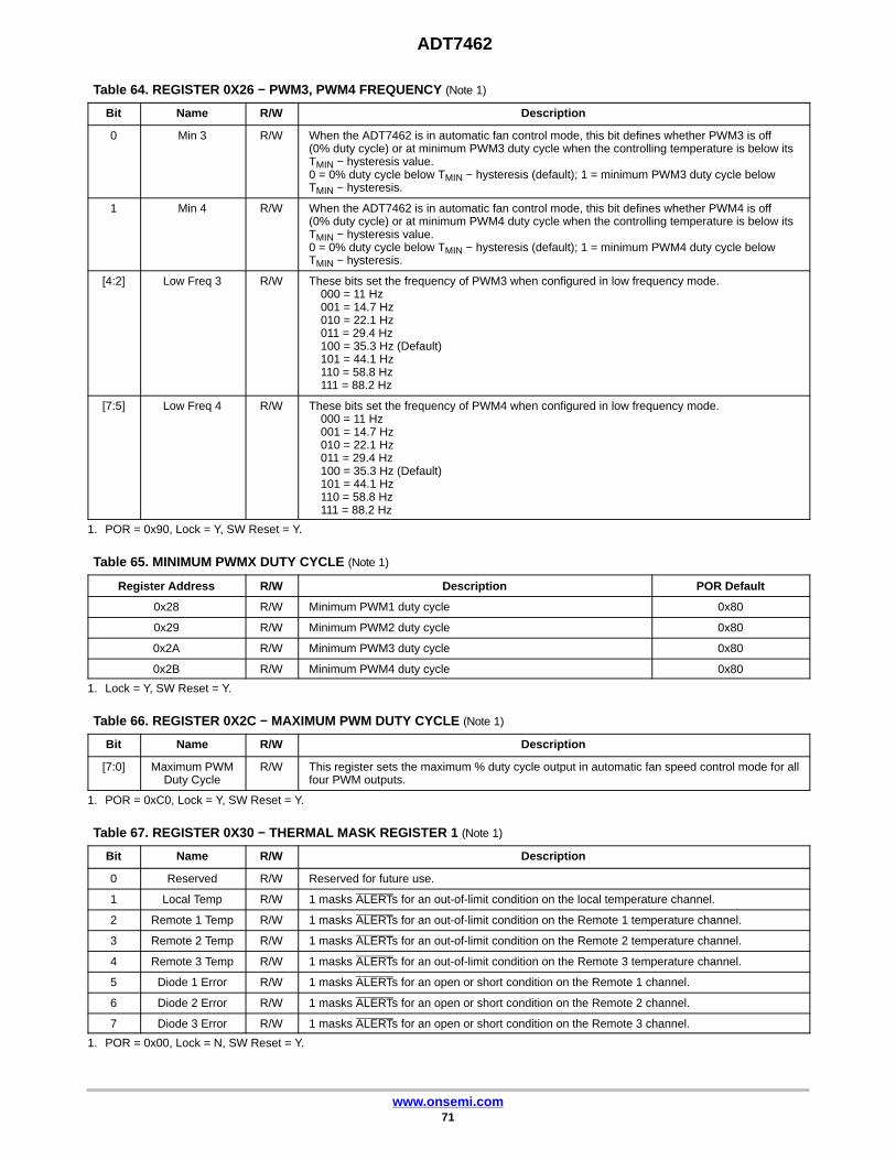
ADT7462
www.onsemi.com71
Table 64. REGISTER 0X26 − PWM3, PWM4 FREQUENCY (Note 1)
Bit Name R/W Description
0 Min 3 R/W When the ADT7462 is in automatic fan control mode, this bit defines whether PWM3 is off(0% duty cycle) or at minimum PWM3 duty cycle when the controlling temperature is below itsTMIN − hysteresis value. 0 = 0% duty cycle below TMIN − hysteresis (default); 1 = minimum PWM3 duty cycle belowTMIN − hysteresis.
1 Min 4 R/W When the ADT7462 is in automatic fan control mode, this bit defines whether PWM4 is off(0% duty cycle) or at minimum PWM4 duty cycle when the controlling temperature is below itsTMIN − hysteresis value. 0 = 0% duty cycle below TMIN − hysteresis (default); 1 = minimum PWM4 duty cycle belowTMIN − hysteresis.
[4:2] Low Freq 3 R/W These bits set the frequency of PWM3 when configured in low frequency mode.000 = 11 Hz001 = 14.7 Hz010 = 22.1 Hz011 = 29.4 Hz100 = 35.3 Hz (Default)101 = 44.1 Hz110 = 58.8 Hz111 = 88.2 Hz
[7:5] Low Freq 4 R/W These bits set the frequency of PWM4 when configured in low frequency mode.000 = 11 Hz001 = 14.7 Hz010 = 22.1 Hz011 = 29.4 Hz100 = 35.3 Hz (Default)101 = 44.1 Hz110 = 58.8 Hz111 = 88.2 Hz
1. POR = 0x90, Lock = Y, SW Reset = Y.
Table 65. MINIMUM PWMX DUTY CYCLE (Note 1)
Register Address R/W Description POR Default
0x28 R/W Minimum PWM1 duty cycle 0x80
0x29 R/W Minimum PWM2 duty cycle 0x80
0x2A R/W Minimum PWM3 duty cycle 0x80
0x2B R/W Minimum PWM4 duty cycle 0x80
1. Lock = Y, SW Reset = Y.
Table 66. REGISTER 0X2C − MAXIMUM PWM DUTY CYCLE (Note 1)
Bit Name R/W Description
[7:0] Maximum PWMDuty Cycle
R/W This register sets the maximum % duty cycle output in automatic fan speed control mode for allfour PWM outputs.
1. POR = 0xC0, Lock = Y, SW Reset = Y.
Table 67. REGISTER 0X30 − THERMAL MASK REGISTER 1 (Note 1)
Bit Name R/W Description
0 Reserved R/W Reserved for future use.
1 Local Temp R/W 1 masks ALERTs for an out-of-limit condition on the local temperature channel.
2 Remote 1 Temp R/W 1 masks ALERTs for an out-of-limit condition on the Remote 1 temperature channel.
3 Remote 2 Temp R/W 1 masks ALERTs for an out-of-limit condition on the Remote 2 temperature channel.
4 Remote 3 Temp R/W 1 masks ALERTs for an out-of-limit condition on the Remote 3 temperature channel.
5 Diode 1 Error R/W 1 masks ALERTs for an open or short condition on the Remote 1 channel.
6 Diode 2 Error R/W 1 masks ALERTs for an open or short condition on the Remote 2 channel.
7 Diode 3 Error R/W 1 masks ALERTs for an open or short condition on the Remote 3 channel.
1. POR = 0x00, Lock = N, SW Reset = Y.

ADT7462
www.onsemi.com72
Table 68. REGISTER 0X31 − THERMAL MASK REGISTER 2 (Note 1)
Bit Name R/W Description
0 THERM1 % R/W 1 masks ALERTs for the corresponding interrupt status bit. Default = 0.
1 THERM1 Assert R/W 1 masks ALERTs for the corresponding interrupt status bit. Default = 0.
2 THERM1 State R/W 1 masks ALERTs for the corresponding interrupt status bit. Default = 0.
3 THERM2 % R/W 1 masks ALERTs for the corresponding interrupt status bit. Default = 0.
4 THERM2 Assert R/W 1 masks ALERTs for the corresponding interrupt status bit. Default = 0.
5 THERM2 State R/W 1 masks ALERTs for the corresponding interrupt status bit. Default = 0.
6 VRD1_Assert R/W 1 masks ALERTs for the corresponding interrupt status bit. Default = 1.
7 VRD2_Assert R/W 1 masks ALERTs for the corresponding interrupt status bit. Default = 1.
1. POR = 0xC0, Lock = N, SW Reset = Y.
Table 69. REGISTER 0X32 − VOLTAGE MASK REGISTER 1 (Note 1)
Bit Name R/W Description
0 +12V1 R/W 1 masks ALERTs for the corresponding interrupt status bit.
1 +12V2 R/W 1 masks ALERTs for the corresponding interrupt status bit.
2 +12V3 R/W 1 masks ALERTs for the corresponding interrupt status bit.
3 +3.3V R/W 1 masks ALERTs for the corresponding interrupt status bit.
4 Pin 15 Voltage R/W 1 masks ALERTs for the corresponding interrupt status bit.
5 Pin 19 Voltage R/W 1 masks ALERTs for the corresponding interrupt status bit.
6 +5V R/W 1 masks ALERTs for the corresponding interrupt status bit.
7 Pin 23 Voltage R/W 1 masks ALERTs for the corresponding interrupt status bit.
1. POR = 0x00, Lock = N, SW Reset = Y.
Table 70. REGISTER 0X33 − VOLTAGE MASK REGISTER 2 (Note 1)
Bit Name R/W Description
[2:0] Reserved R/W Reserved for future use.
3 Pin 24 Voltage R/W 1 masks ALERTs for the corresponding interrupt status bit.
4 Pin 25 Voltage R/W 1 masks ALERTs for the corresponding interrupt status bit.
5 Pin 26 Voltage R/W 1 masks ALERTs for the corresponding interrupt status bit.
6 +1.5V2 (3GIO) R/W 1 masks ALERTs for the corresponding interrupt status bit.
7 +1.5V1 (ICH) R/W 1 masks ALERTs for the corresponding interrupt status bit.
1. POR = 0x00, Lock = N, SW Reset = Y.
Table 71. REGISTER 0X34 − FAN MASK REGISTER (Note 1)
Bit Name R/W Description
0 Fan 1 Fault R/W 1 masks ALERTs for the corresponding interrupt status bit.
1 Fan 2 Fault R/W 1 masks ALERTs for the corresponding interrupt status bit.
2 Fan 3 Fault R/W 1 masks ALERTs for the corresponding interrupt status bit.
3 Fan 4 Fault R/W 1 masks ALERTs for the corresponding interrupt status bit.
4 Fan 5 Fault R/W 1 masks ALERTs for the corresponding interrupt status bit.
5 Fan 6 Fault R/W 1 masks ALERTs for the corresponding interrupt status bit.
6 Fan 7 Fault R/W 1 masks ALERTs for the corresponding interrupt status bit.
7 Fan 8 Fault R/W 1 masks ALERTs for the corresponding interrupt status bit.
1. POR = 0x00, Lock = N, SW Reset = Y.
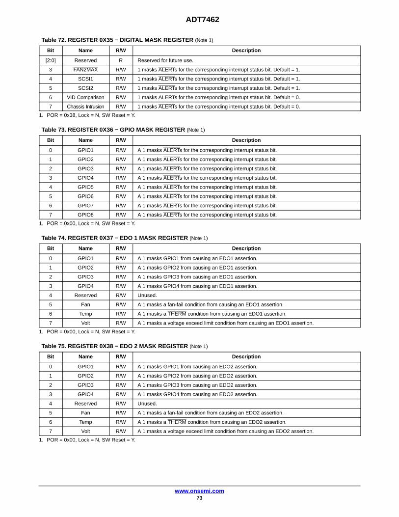
ADT7462
www.onsemi.com73
Table 72. REGISTER 0X35 − DIGITAL MASK REGISTER (Note 1)
Bit Name R/W Description
[2:0] Reserved R Reserved for future use.
3 FAN2MAX R/W 1 masks ALERTs for the corresponding interrupt status bit. Default = 1.
4 SCSI1 R/W 1 masks ALERTs for the corresponding interrupt status bit. Default = 1.
5 SCSI2 R/W 1 masks ALERTs for the corresponding interrupt status bit. Default = 1.
6 VID Comparison R/W 1 masks ALERTs for the corresponding interrupt status bit. Default = 0.
7 Chassis Intrusion R/W 1 masks ALERTs for the corresponding interrupt status bit. Default = 0.
1. POR = 0x38, Lock = N, SW Reset = Y.
Table 73. REGISTER 0X36 − GPIO MASK REGISTER (Note 1)
Bit Name R/W Description
0 GPIO1 R/W A 1 masks ALERTs for the corresponding interrupt status bit.
1 GPIO2 R/W A 1 masks ALERTs for the corresponding interrupt status bit.
2 GPIO3 R/W A 1 masks ALERTs for the corresponding interrupt status bit.
3 GPIO4 R/W A 1 masks ALERTs for the corresponding interrupt status bit.
4 GPIO5 R/W A 1 masks ALERTs for the corresponding interrupt status bit.
5 GPIO6 R/W A 1 masks ALERTs for the corresponding interrupt status bit.
6 GPIO7 R/W A 1 masks ALERTs for the corresponding interrupt status bit.
7 GPIO8 R/W A 1 masks ALERTs for the corresponding interrupt status bit.
1. POR = 0x00, Lock = N, SW Reset = Y.
Table 74. REGISTER 0X37 − EDO 1 MASK REGISTER (Note 1)
Bit Name R/W Description
0 GPIO1 R/W A 1 masks GPIO1 from causing an EDO1 assertion.
1 GPIO2 R/W A 1 masks GPIO2 from causing an EDO1 assertion.
2 GPIO3 R/W A 1 masks GPIO3 from causing an EDO1 assertion.
3 GPIO4 R/W A 1 masks GPIO4 from causing an EDO1 assertion.
4 Reserved R/W Unused.
5 Fan R/W A 1 masks a fan-fail condition from causing an EDO1 assertion.
6 Temp R/W A 1 masks a THERM condition from causing an EDO1 assertion.
7 Volt R/W A 1 masks a voltage exceed limit condition from causing an EDO1 assertion.
1. POR = 0x00, Lock = N, SW Reset = Y.
Table 75. REGISTER 0X38 − EDO 2 MASK REGISTER (Note 1)
Bit Name R/W Description
0 GPIO1 R/W A 1 masks GPIO1 from causing an EDO2 assertion.
1 GPIO2 R/W A 1 masks GPIO2 from causing an EDO2 assertion.
2 GPIO3 R/W A 1 masks GPIO3 from causing an EDO2 assertion.
3 GPIO4 R/W A 1 masks GPIO4 from causing an EDO2 assertion.
4 Reserved R/W Unused.
5 Fan R/W A 1 masks a fan-fail condition from causing an EDO2 assertion.
6 Temp R/W A 1 masks a THERM condition from causing an EDO2 assertion.
7 Volt R/W A 1 masks a voltage exceed limit condition from causing an EDO2 assertion.
1. POR = 0x00, Lock = N, SW Reset = Y.
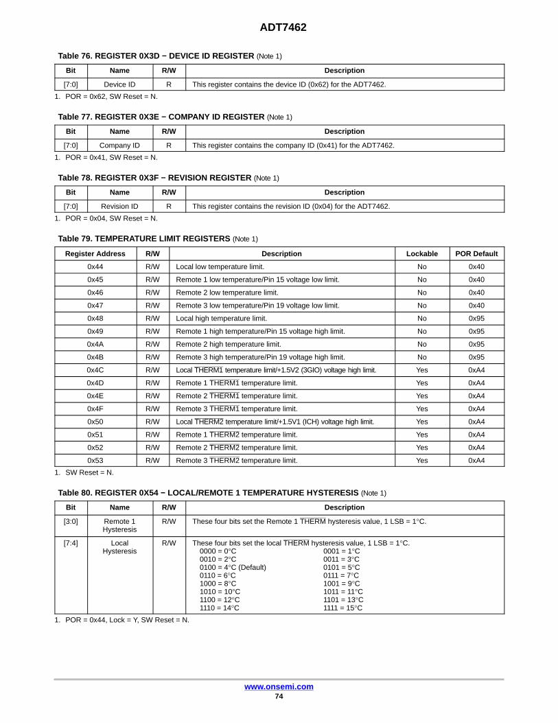
ADT7462
www.onsemi.com74
Table 76. REGISTER 0X3D − DEVICE ID REGISTER (Note 1)
Bit Name R/W Description
[7:0] Device ID R This register contains the device ID (0x62) for the ADT7462.
1. POR = 0x62, SW Reset = N.
Table 77. REGISTER 0X3E − COMPANY ID REGISTER (Note 1)
Bit Name R/W Description
[7:0] Company ID R This register contains the company ID (0x41) for the ADT7462.
1. POR = 0x41, SW Reset = N.
Table 78. REGISTER 0X3F − REVISION REGISTER (Note 1)
Bit Name R/W Description
[7:0] Revision ID R This register contains the revision ID (0x04) for the ADT7462.
1. POR = 0x04, SW Reset = N.
Table 79. TEMPERATURE LIMIT REGISTERS (Note 1)
Register Address R/W Description Lockable POR Default
0x44 R/W Local low temperature limit. No 0x40
0x45 R/W Remote 1 low temperature/Pin 15 voltage low limit. No 0x40
0x46 R/W Remote 2 low temperature limit. No 0x40
0x47 R/W Remote 3 low temperature/Pin 19 voltage low limit. No 0x40
0x48 R/W Local high temperature limit. No 0x95
0x49 R/W Remote 1 high temperature/Pin 15 voltage high limit. No 0x95
0x4A R/W Remote 2 high temperature limit. No 0x95
0x4B R/W Remote 3 high temperature/Pin 19 voltage high limit. No 0x95
0x4C R/W Local THERM1 temperature limit/+1.5V2 (3GIO) voltage high limit. Yes 0xA4
0x4D R/W Remote 1 THERM1 temperature limit. Yes 0xA4
0x4E R/W Remote 2 THERM1 temperature limit. Yes 0xA4
0x4F R/W Remote 3 THERM1 temperature limit. Yes 0xA4
0x50 R/W Local THERM2 temperature limit/+1.5V1 (ICH) voltage high limit. Yes 0xA4
0x51 R/W Remote 1 THERM2 temperature limit. Yes 0xA4
0x52 R/W Remote 2 THERM2 temperature limit. Yes 0xA4
0x53 R/W Remote 3 THERM2 temperature limit. Yes 0xA4
1. SW Reset = N.
Table 80. REGISTER 0X54 − LOCAL/REMOTE 1 TEMPERATURE HYSTERESIS (Note 1)
Bit Name R/W Description
[3:0] Remote 1Hysteresis
R/W These four bits set the Remote 1 THERM hysteresis value, 1 LSB = 1°C.
[7:4] LocalHysteresis
R/W These four bits set the local THERM hysteresis value, 1 LSB = 1°C.0000 = 0°C 0001 = 1°C0010 = 2°C 0011 = 3°C0100 = 4°C (Default) 0101 = 5°C0110 = 6°C 0111 = 7°C1000 = 8°C 1001 = 9°C1010 = 10°C 1011 = 11°C1100 = 12°C 1101 = 13°C1110 = 14°C 1111 = 15°C
1. POR = 0x44, Lock = Y, SW Reset = N.
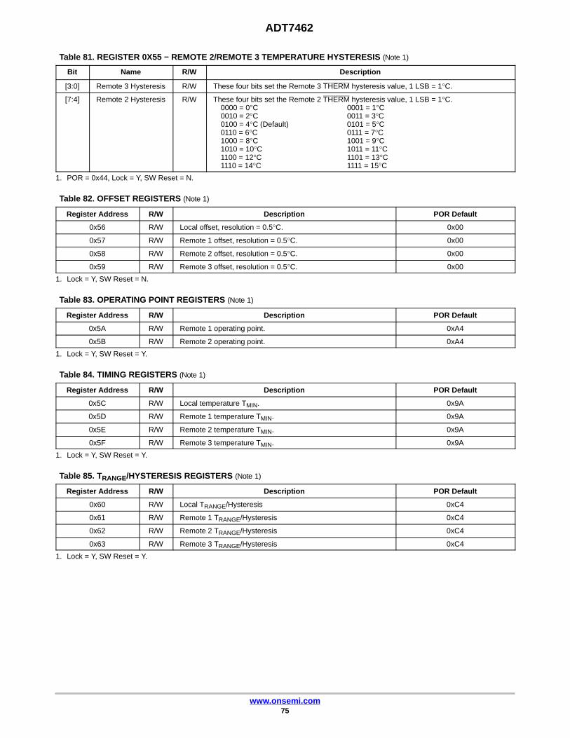
ADT7462
www.onsemi.com75
Table 81. REGISTER 0X55 − REMOTE 2/REMOTE 3 TEMPERATURE HYSTERESIS (Note 1)
Bit Name R/W Description
[3:0] Remote 3 Hysteresis R/W These four bits set the Remote 3 THERM hysteresis value, 1 LSB = 1°C.
[7:4] Remote 2 Hysteresis R/W These four bits set the Remote 2 THERM hysteresis value, 1 LSB = 1°C.0000 = 0°C 0001 = 1°C0010 = 2°C 0011 = 3°C0100 = 4°C (Default) 0101 = 5°C0110 = 6°C 0111 = 7°C1000 = 8°C 1001 = 9°C1010 = 10°C 1011 = 11°C1100 = 12°C 1101 = 13°C1110 = 14°C 1111 = 15°C
1. POR = 0x44, Lock = Y, SW Reset = N.
Table 82. OFFSET REGISTERS (Note 1)
Register Address R/W Description POR Default
0x56 R/W Local offset, resolution = 0.5°C. 0x00
0x57 R/W Remote 1 offset, resolution = 0.5°C. 0x00
0x58 R/W Remote 2 offset, resolution = 0.5°C. 0x00
0x59 R/W Remote 3 offset, resolution = 0.5°C. 0x00
1. Lock = Y, SW Reset = N.
Table 83. OPERATING POINT REGISTERS (Note 1)
Register Address R/W Description POR Default
0x5A R/W Remote 1 operating point. 0xA4
0x5B R/W Remote 2 operating point. 0xA4
1. Lock = Y, SW Reset = Y.
Table 84. TIMING REGISTERS (Note 1)
Register Address R/W Description POR Default
0x5C R/W Local temperature TMIN. 0x9A
0x5D R/W Remote 1 temperature TMIN. 0x9A
0x5E R/W Remote 2 temperature TMIN. 0x9A
0x5F R/W Remote 3 temperature TMIN. 0x9A
1. Lock = Y, SW Reset = Y.
Table 85. TRANGE/HYSTERESIS REGISTERS (Note 1)
Register Address R/W Description POR Default
0x60 R/W Local TRANGE/Hysteresis 0xC4
0x61 R/W Remote 1 TRANGE/Hysteresis 0xC4
0x62 R/W Remote 2 TRANGE/Hysteresis 0xC4
0x63 R/W Remote 3 TRANGE/Hysteresis 0xC4
1. Lock = Y, SW Reset = Y.

ADT7462
www.onsemi.com76
Table 86. REGISTER 0X60, REGISTER 61, REGISTER 62, REGISTER 63 − LOCAL, REMOTE 1, REMOTE 2, AND REMOTE 3 TRANGE/HYSTERESIS
Bit Name R/W Description
[3:0] Hysteresis R/W These four bits set the hysteresis in the automatic fan speed control loop and in the dynamicTMIN control loop, 1 LSB = 1°C.
0000 = 0°C 0001 = 1°C0010 = 2°C 0011 = 3°C0100 = 4°C (Default) 0101 = 5°C0110 = 6°C 0111 = 7°C1000 = 8°C 1001 = 9°C1010 = 10°C 1011 = 11°C1100 = 12°C 1101 = 13°C1110 = 14°C 1111 = 15°C
[7:4] Range R/W These four bits set the TRANGE value, that is, the slope or rate of change of fan speed withrespect to temperature in the automatic fan speed control loop.
0000 = 2°C 0001 = 2.5°C0010 = 3.3°C 0011 = 4°C0100 = 5°C 0101 = 6.7°C0110 = 8°C 0111 = 10°C1000 = 13.3°C 1001 = 16°C1010 = 20°C 1011 = 26.7°C1100 = 32°C (Default) 1101 = 40°C1110 = 53.3°C 1111 = 80°C
Table 87. REGISTER 0X64 − OPERATING POINT HYSTERESIS (Note 1)
Bit Name R/W Description
[3:0] Reserved R Reserved for future use.
[7:4] Operating PointHysteresis
R/W These four bits set the operating point hysteresis for the dynamic TMIN control loop,1 LSB = 1°C.
0000 = 0°C 0001 = 1°C0010 = 2°C 0011 = 3°C0100 = 4°C (Default) 0101 = 5°C0110 = 6°C 0111 = 7°C1000 = 8°C 1001 = 9°C1010 = 10°C 1011 = 11°C1100 = 12°C 1101 = 13°C1110 = 14°C 1111 = 15°C
1. POR = 0x40, Lock = Y, SW Reset = Y.
Table 88. VOLTAGE LIMIT REGISTERS (Note 1)
Register Address R/W Description POR Default
0x68 R/W +3.3V high limit. 0xFF
0x69 R/W Pin 23 voltage high limit. 0xFF
0x6A R/W Pin 24 voltage high limit. 0xFF
0x6B R/W Pin 25 voltage high limit. 0xFF
0x6C R/W Pin 26 voltage high limit. 0xFF
0x6D R/W +12V1 voltage low limit. 0x00
0x6E R/W +12V2 voltage low limit. 0x00
0x6F R/W +12V3 voltage low limit. 0x00
0x70 R/W +3.3V low limit. 0x00
0x71 R/W +5V low limit. 0x00
0x72 R/W Pin 23 voltage low limit. 0x20
0x73 R/W Pin 24 voltage low limit. 0x00
0x74 R/W Pin 25 voltage low limit. 0x00
0x75 R/W Pin 26 voltage low limit. 0x80
0x76 R/W +1.5V2 (3GIO) voltage low limit. 0x00
0x77 R/W +1.5V1 (ICH) voltage low limit. 0x00
1. Lock = N, SW Reset = N.

ADT7462
www.onsemi.com77
Table 89. TACH LIMIT REGISTERS (Note 1)
Register Address R/W Description POR Default
0x78 R/W TACH1 limit/VID limit. 0xFF
0x79 R/W TACH2 limit. 0xFF
0x7A R/W TACH3 limit. 0xFF
0x7B R/W TACH4 limit. 0xFF
0x7C R/W TACH5 limit/+12V1 voltage high limit. 0xFF
0x7D R/W TACH6 limit/+12V2 voltage high limit. 0xFF
0x7E R/W TACH7 limit/+5V voltage high limit. 0xFF
0x7F R/W TACH8 limit/+12V3 voltage high limit. 0xFF
1. Lock = Y, SW Reset = N.
Table 90. THERM TIMER LIMIT REGISTERS (Note 1)
Register Address R/W Description POR Default
0x80 R/W THERM1 Timer Limit. 0xFF
0x81 R/W THERM2 Timer Limit. 0xFF
1. Lock = Y, SW Reset = N.
Table 91. TEMPERATURE VALUE REGISTERS (Note 1)
Register Address R/W Description POR Default
0x88 R Bits [7:6] Local temperature value, LSBs. 0x00
0x89 R Local temperature value, MSBs. 0x00
0x8A R Bits [7:6] Remote 1 temperature value, LSBs. 0x00
0x8B R Remote 1 temperature value, MSBs/Pin 15 voltage. 0x00
0x8C R Bits [7:6] Remote 2 temperature value, LSBs. 0x00
0x8D R Remote 2 temperature value, MSBs. 0x00
0x8E R Bits [7:6] Remote 3 temperature value, LSBs. 0x00
0x8F R Remote 3 temperature value, MSBs/Pin 19 voltage. 0x00
1. Lock = N, SW Reset = N.
Table 92. VOLTAGE VALUE REGISTERS (Note 1)
Register Address R/W Description POR Default
0x90 R Pin 23 voltage value. 0x00
0x91 R Pin 24 voltage value. 0x00
0x92 R Pin 25 voltage value. 0x00
0x93 R Pin 26 voltage value. 0x00
0x94 R +1.5V1 (ICH) voltage value. 0x00
0x95 R +1.5V2 (3GIO) voltage value. 0x00
0x96 R +3.3V voltage value. 0x00
1. Lock = N, SW Reset = N.
Table 93. VID VALUE REGISTERS (Note 1)
Register Address R/W Description POR Default
0x97 R This register reports the state of the seven VID inputs. 0x00
1. Lock = N, SW Reset = N.

ADT7462
www.onsemi.com78
Table 94. TACH VALUE REGISTERS (Note 1)
Register Address R/W Description POR Default
0x98 R TACH1, LSB. 0xFF
0x99 R TACH1, MSB. 0xFF
0x9A R TACH2, LSB. 0xFF
0x9B R TACH2, MSB. 0xFF
0x9C R TACH3, LSB. 0xFF
0x9D R TACH3, MSB. 0xFF
0x9E R TACH4, LSB. 0xFF
0x9F R TACH4, MSB. 0xFF
0xA2 R TACH5, LSB. 0xFF
0xA3 R TACH5, MSB/+12V1 voltage value register. 0xFF
0xA4 R TACH6, LSB. 0xFF
0xA5 R TACH6, MSB/+12V2 voltage value register. 0xFF
0xA6 R TACH7, LSB. 0xFF
0xA7 R TACH7, MSB/+5V voltage value register. 0xFF
0xA8 R TACH8, LSB. 0xFF
0xA9 R TACH8, MSB/+12V3 voltage value register. 0xFF
1. Lock = N, SW Reset = N.
Table 95. PWM CURRENT DUTY CYCLE REGISTERS (Note 1)
Register Address R/W Description POR Default
0xAA R/W PWM1 current duty cycle. 0x00
0xAB R/W PWM2 current duty cycle. 0x00
0xAC R/W PWM3 current duty cycle. 0xC0
0xAD R/W PWM4 current duty cycle. 0x00
1. Lock = N, SW Reset = N.
Table 96. THERM TIMER VALUE REGISTERS (Note 1)
Register Address R/W Description POR Default
0xAE R THERM1 timer % on-time value. 0x00
0xAF R THERM2 timer % on-time value. 0x00
1. Lock = N, SW Reset = N.
Table 97. REGISTER 0XB8 − HOST THERMAL STATUS REGISTER 1 (Note 1);REGISTER 0XC0 − BMC THERMAL STATUS REGISTER 1 (Note 1)
Bit Name R/W Description
0 Reserved R Reserved for future use.
1 Local Temp R A 1 indicates that a local temperature limit has been tripped.
2 Remote 1 Temp R A 1 indicates that a Remote 1 temperature limit has been tripped.
3 Remote 2 Temp R A 1 indicates that a Remote 2 temperature limit has been tripped.
4 Remote 3 Temp R A 1 indicates that a Remote 3 temperature limit has been tripped.
5 Diode 1 Error R A 1 indicates that a Remote 1 diode error, either an open or a short, has occurred.
6 Diode 2 Error R A 1 indicates that a Remote 2 diode error, either an open or a short, has occurred.
7 Diode 3 Error R A 1 indicates that a Remote 3 diode error, either an open or a short, has occurred.
1. POR = 0x00, Lock = N, SW Reset = Y.

ADT7462
www.onsemi.com79
Table 98. REGISTER 0XB9 − HOST THERMAL STATUS REGISTER 2 (Note 1);REGISTER 0XC1 − BMC THERMAL STATUS REGISTER 2 (Note 1)
Bit Name R/W Description
0 THERM1 % R A 1 indicates that THERM1 has been asserted for longer than the programmed THERM1 timerlimit.
1 THERM1 Assert R A 1 indicates that THERM1 is asserted.
2 THERM1 State R A 1 indicates that a transition from high to low has taken place on the THERM1 pin.
3 THERM2 % R A 1 indicates that THERM2 has been asserted for longer than the programmed THERM2 timerlimit.
4 THERM2 Assert R A 1 indicates that THERM2 is asserted.
5 THERM2 State R A 1 indicates that a transition from high to low has taken place on the THERM2 pin.
6 VRD1_Assert R A 1 indicates that VRD1 is asserted.
7 VRD2_Assert R A 1 indicates that VRD2 is asserted.
1. POR = 0x00, Lock = N, SW Reset = Y.
Table 99. REGISTER 0XBA − HOST THERMAL STATUS REGISTER 3 (Note 1)
Bit Name R/W Description
0 Local THERM1 R A 1 indicates that the local THERM1 limit has been exceeded.
1 Remote 1THERM1
R A 1 indicates that the Remote 1 THERM1 limit has been exceeded.
2 Remote 2THERM1
R A 1 indicates that the Remote 2 THERM1 limit has been exceeded.
3 Remote 3THERM1
R A 1 indicates that the Remote 3 THERM1 limit has been exceeded.
4 Local THERM2 R A 1 indicates that the Local THERM2 limit has been exceeded.
5 Remote 1THERM2
R A 1 indicates that the Remote 1 THERM2 limit has been exceeded.
6 Remote 2THERM2
R A 1 indicates that the Remote 2 THERM2 limit has been exceeded.
7 Remote 3THERM2
R A 1 indicates that the Remote 3 THERM2 limit has been exceeded.
1. POR = 0x00, Lock = N, SW Reset = Y.
Table 100. REGISTER 0XBB − HOST VOLTAGE STATUS REGISTER 1 (Note 1);REGISTER 0XC3 − BMC VOLTAGE REGISTER 1 (Note 1)
Bit Name R/W Description
0 +12V1 R A 1 indicates that a +12V1 voltage limit has been tripped.
1 +12V2 R A 1 indicates that a +12V2 voltage limit has been tripped.
2 +12V3 R A 1 indicates that a +12V3 voltage limit has been tripped.
3 +3.3V R A 1 indicates that a +3.3V voltage limit has been tripped.
4 Pin 15 Voltage R A 1 indicates that a Pin 15 voltage limit has been tripped.
5 Pin 19 Voltage R A 1 indicates that a Pin 19 voltage limit has been tripped.
6 +5V R A 1 indicates that a +5V voltage limit has been tripped.
7 Pin 23 Voltage R A 1 indicates that a Pin 23 voltage limit has been tripped.
1. POR = 0x00, Lock = N, SW Reset = Y.

ADT7462
www.onsemi.com80
Table 101. REGISTER 0XBC − HOST VOLTAGE STATUS REGISTER 2 (Note 1);REGISTER 0XC4 − BMC VOLTAGE STATUS REGISTER 2 (Note 1)
Bit Name R/W Description
[2:0] Reserved R Reserved for future use.
3 Pin 24 Voltage R A 1 indicates that a Pin 24 voltage limit has been tripped.
4 Pin 25 Voltage R A 1 indicates that a Pin 25 voltage limit has been tripped.
5 Pin 26 Voltage R A 1 indicates that a Pin 26 voltage limit has been tripped.
6 +1.5V2 (3GIO) R A 1 indicates that a +1.5V2 (3GIO) voltage limit has been tripped.
7 +1.5V1 (ICH) R A 1 indicates that a +1.5V1 (ICH) voltage limit has been tripped.
1. POR = 0x00, Lock = N, SW Reset = Y.
Table 102. REGISTER 0XBD − HOST FAN STATUS REGISTER (Note 1);REGISTER 0XC5 − BMC FAN STATUS REGISTER (Note 1)
Bit Name R/W Description
0 Fan 1 Fault R A 1 indicates a Fan 1 fault.
1 Fan 2 Fault R A 1 indicates a Fan 2 fault.
2 Fan 3 Fault R A 1 indicates a Fan 3 fault.
3 Fan 4 Fault R A 1 indicates a Fan 4 fault.
4 Fan 5 Fault R A 1 indicates a Fan 5 fault.
5 Fan 6 Fault R A 1 indicates a Fan 6 fault.
6 Fan 7 Fault R A 1 indicates a Fan 7 fault.
7 Fan 8 Fault R A 1 indicates a Fan 8 fault.
1. POR = 0x00, Lock = N, SW Reset = Y.
Table 103. REGISTER 0XBE − HOST DIGITAL STATUS REGISTER (Note 1);REGISTER 0XC6 − BMC DIGITAL STATUS REGISTER (Note 1)
Bit Name R/W Description
[2:0] Reserved R Reserved for future use.
3 FAN2MAX R A 1 indicates that the FAN2MAX has been asserted as an input.
4 SCSI1 R A 1 indicates that the SCSI_TERM1 digital input has been asserted.
5 SCSI2 R A 1 indicates that the SCSI_TERM2 digital input has been asserted.
6 VID Comparison R A 1 indicates a VID comparison fault.
7 Chassis Intrusion R A 1 indicates that the chassis intrusion digital input has been asserted.
1. POR = 0x00, Lock = N, SW Reset = Y.
Table 104. REGISTER 0XBF − HOST GPIO STATUS REGISTER (Note 1)
Bit Name R/W Description
0 GPIO1 R/W A 1 indicates that GPIO1 is asserted.
1 GPIO2 R/W A 1 indicates that GPIO2 is asserted.
2 GPIO3 R/W A 1 indicates that GPIO3 is asserted.
3 GPIO4 R/W A 1 indicates that GPIO4 is asserted.
4 GPIO5 R/W A 1 indicates that GPIO5 is asserted.
5 GPIO6 R/W A 1 indicates that GPIO6 is asserted.
6 GPIO7 R/W A 1 indicates that GPIO7 is asserted.
7 GPIO8 R/W A 1 indicates that GPIO8 is asserted.
1. POR = 0x00, Lock = N, SW Reset = Y.

ADT7462
www.onsemi.com81
Table 105. ORDERING INFORMATION
Device Number* Temperature Range Package Type Package Option Shipping†
ADT7462ACPZ−REEL −40°C to +125°C 32-lead LFCSP_VQ CP−32−2 5,000 Tape & Reel
†For information on tape and reel specifications, including part orientation and tape sizes, please refer to our Tape and Reel PackagingSpecifications Brochure, BRD8011/D.
*The “Z’’ suffix indicates Pb−Free part.
Pentium is a registered trademark of Intel Corporation.

LFCSP32 5x5, 0.5PCASE 932AE−01
ISSUE ADATE 27 JAN 2009
SCALE 2:1
SEATING
NOTE 4
M
0.20 C
(A3)
A
A1
D2
b
1
9
17
32
E2
32X
4X
L32X
BOTTOM VIEW
INDICATOR
TOP VIEW
SIDE VIEW
D AB
E
0.20 C
PIN ONEREFERENCE
0.10 C
0.08 C
C
25
e A0.10 BC
0.05 C
NOTES:1. DIMENSIONING AND TOLERANCING PER
ASME Y14.5M, 1994.2. CONTROLLING DIMENSIONS: MILLIMETERS.3. DIMENSION b APPLIES TO PLATED
TERMINAL AND IS MEASURED BETWEEN0.15 AND 0.30mm FROM THE TERMINAL TIP.
4. COPLANARITY APPLIES TO THE EXPOSEDPAD AS WELL AS THE TERMINALS.
DIM MIN MAXMILLIMETERS
A 0.80 1.00A1 0.00 0.05A3 0.20 REFb 0.18 0.30D 5.00 BSC
D2 2.95 3.25E 5.00 BSC
3.25E2 2.95e 0.50 BSCH −−− 12K 0.20 −−−
PLANE
DIMENSIONS: MILLIMETERS
0.50
3.14
0.28
3.14
32X
0.6332X
5.30
5.30
*For additional information on our Pb−Free strategy and solderingdetails, please download the ON Semiconductor Soldering andMounting Techniques Reference Manual, SOLDERRM/D.
SOLDERING FOOTPRINT*
1
L 0.30 0.50M −−− 0.60
D1 4.75 BSC
E1 4.75 BSC
D1
E1
H
PITCH
PACKAGEOUTLINE
PIN 1
M4X
K
°
NOTE 3
MECHANICAL CASE OUTLINE
PACKAGE DIMENSIONS
ON Semiconductor and are trademarks of Semiconductor Components Industries, LLC dba ON Semiconductor or its subsidiaries in the United States and/or other countries.ON Semiconductor reserves the right to make changes without further notice to any products herein. ON Semiconductor makes no warranty, representation or guarantee regardingthe suitability of its products for any particular purpose, nor does ON Semiconductor assume any liability arising out of the application or use of any product or circuit, and specificallydisclaims any and all liability, including without limitation special, consequential or incidental damages. ON Semiconductor does not convey any license under its patent rights nor therights of others.
98AON26684DDOCUMENT NUMBER:
DESCRIPTION:
Electronic versions are uncontrolled except when accessed directly from the Document Repository.Printed versions are uncontrolled except when stamped “CONTROLLED COPY” in red.
PAGE 1 OF 1LFCSP32, 5x5, 0.5P
© Semiconductor Components Industries, LLC, 2019 www.onsemi.com

onsemi, , and other names, marks, and brands are registered and/or common law trademarks of Semiconductor Components Industries, LLC dba “onsemi” or its affiliatesand/or subsidiaries in the United States and/or other countries. onsemi owns the rights to a number of patents, trademarks, copyrights, trade secrets, and other intellectual property.A listing of onsemi’s product/patent coverage may be accessed at www.onsemi.com/site/pdf/Patent−Marking.pdf. onsemi reserves the right to make changes at any time to anyproducts or information herein, without notice. The information herein is provided “as−is” and onsemi makes no warranty, representation or guarantee regarding the accuracy of theinformation, product features, availability, functionality, or suitability of its products for any particular purpose, nor does onsemi assume any liability arising out of the application or useof any product or circuit, and specifically disclaims any and all liability, including without limitation special, consequential or incidental damages. Buyer is responsible for its productsand applications using onsemi products, including compliance with all laws, regulations and safety requirements or standards, regardless of any support or applications informationprovided by onsemi. “Typical” parameters which may be provided in onsemi data sheets and/or specifications can and do vary in different applications and actual performance mayvary over time. All operating parameters, including “Typicals” must be validated for each customer application by customer’s technical experts. onsemi does not convey any licenseunder any of its intellectual property rights nor the rights of others. onsemi products are not designed, intended, or authorized for use as a critical component in life support systemsor any FDA Class 3 medical devices or medical devices with a same or similar classification in a foreign jurisdiction or any devices intended for implantation in the human body. ShouldBuyer purchase or use onsemi products for any such unintended or unauthorized application, Buyer shall indemnify and hold onsemi and its officers, employees, subsidiaries, affiliates,and distributors harmless against all claims, costs, damages, and expenses, and reasonable attorney fees arising out of, directly or indirectly, any claim of personal injury or deathassociated with such unintended or unauthorized use, even if such claim alleges that onsemi was negligent regarding the design or manufacture of the part. onsemi is an EqualOpportunity/Affirmative Action Employer. This literature is subject to all applicable copyright laws and is not for resale in any manner.
PUBLICATION ORDERING INFORMATIONTECHNICAL SUPPORTNorth American Technical Support:Voice Mail: 1 800−282−9855 Toll Free USA/CanadaPhone: 011 421 33 790 2910
LITERATURE FULFILLMENT:Email Requests to: [email protected]
onsemi Website: www.onsemi.com
Europe, Middle East and Africa Technical Support:Phone: 00421 33 790 2910For additional information, please contact your local Sales Representative
◊