adv7842 hw manual rev pra€¦ · 5.5.1 manual input muxing ... 211 7.37 background port infoframe...
TRANSCRIPT

ADV7850
Fast Switching 4:1 HDMI 1.4 Receiver With 3D-Comb Decoder and Digitizer
HARDWARE MANUAL
Rev. A
May 2012

ADV7850
Rev. A May 2012 2
TABLE OF CONTENTS 1 INTRODUCTION TO ADV7850 HARDWARE MANUAL ................................................................................................ 11
1.1 DESCRIPTION OF THE HARDWARE MANUAL ...................................................................................................................................... 11 1.2 COPYRIGHT INFORMATION .................................................................................................................................................................. 11 1.3 DISCLAIMER ........................................................................................................................................................................................... 11 1.4 TRADEMARK AND SERVICE MARK NOTICE......................................................................................................................................... 11 1.5 NUMBER NOTATIONS ........................................................................................................................................................................... 11 1.6 REGISTER ACCESS CONVENTIONS ....................................................................................................................................................... 11 1.7 ACRONYMS AND ABBREVIATIONS ....................................................................................................................................................... 11 1.8 CONTROL DESCRIPTION ....................................................................................................................................................................... 13 1.9 REFERENCES ........................................................................................................................................................................................... 14
2 INTRODUCTION ................................................................................................................................................................. 15
2.1 ANALOG FRONT END ............................................................................................................................................................................ 15 2.2 STANDARD DEFINITION PROCESSOR ................................................................................................................................................... 16 2.3 HDMI RECEIVER .................................................................................................................................................................................. 16 2.4 COMPONENT PROCESSOR ..................................................................................................................................................................... 16 2.5 AUDIO CODEC .................................................................................................................................................................................... 17 2.6 MAIN FEATURES OF ADV7850 ............................................................................................................................................................ 17
2.6.1 Analog Front End .............................................................................................................................................................. 17 2.6.2 HDMI Receiver .................................................................................................................................................................. 17 2.6.3 Composite and S-Video Processing ................................................................................................................................... 17 2.6.4 Component Video Processing ............................................................................................................................................ 18 2.6.5 RGB Graphics Processing .................................................................................................................................................. 18 2.6.6 Audio CODEC ................................................................................................................................................................... 18 2.6.7 Additional Features ........................................................................................................................................................... 18
2.7 FUNCTIONAL BLOCK DIAGRAM ........................................................................................................................................................... 19 2.8 PIN DESCRIPTION .................................................................................................................................................................................. 20
3 GLOBAL CONTROL REGISTERS........................................................................................................................................ 29
3.1 ADV7850 REVISION IDENTIFICATION ................................................................................................................................................ 29 3.2 POWER-DOWN CONTROLS ................................................................................................................................................................... 29
3.2.1 Primary Power-down Controls ......................................................................................................................................... 29 3.2.2 Secondary Power-down Controls ...................................................................................................................................... 29 3.2.3 Power-down Mode ............................................................................................................................................................ 30 3.2.4 EDID Support in Power-off Mode.................................................................................................................................... 31 3.2.5 ADC Power-down Control ................................................................................................................................................ 32 3.2.6 DDC and VGA Pins Power Down .................................................................................................................................... 33
3.3 RESET CONTROLS AND GLOBAL PIN CONTROLS ................................................................................................................................. 33 3.3.1 Reset Pin ............................................................................................................................................................................ 33 3.3.2 Reset Controls .................................................................................................................................................................... 33 3.3.3 Tristate Pins ....................................................................................................................................................................... 34 3.3.4 ADC Phase Control ........................................................................................................................................................... 34
3.4 ADC-HDMI SIMULTANEOUS MODE .................................................................................................................................................. 34
4 PRIMARY MODE AND VIDEO STANDARD .................................................................................................................... 36
4.1 PRIMARY MODE AND VIDEO STANDARD CONTROLS ........................................................................................................................ 36 4.1.1 Setting the Vertical Frequency .......................................................................................................................................... 40
4.2 STANDARD CONFIGURATION FOR SDP-HDMI AUDIO SIMULTANEOUS MODE ............................................................................. 40 4.3 PRIMARY MODE AND VIDEO STANDARD CONFIGURATION FOR HDMI FREE RUN ....................................................................... 41

ADV7850
Rev. A May 2012 3
5 ANALOG FRONT END ......................................................................................................................................................... 42
5.1 ADC SAMPLING CLOCK ....................................................................................................................................................................... 42 5.2 ADCS AND VOLTAGE CLAMPS ............................................................................................................................................................ 42
5.2.1 Analog Input Hardware Configuration ............................................................................................................................ 42 5.2.2 Clamp Operation ............................................................................................................................................................... 43 5.2.3 SDP Clamp Operation ....................................................................................................................................................... 43
5.3 ANALOG INPUT MUXING ..................................................................................................................................................................... 45 5.3.1 Analog Input Routing Recommendation .......................................................................................................................... 45
5.4 AUTOMATIC INPUT MUXING SELECTION ........................................................................................................................................... 46 5.5 MANUAL INPUT MUXING OVERVIEW ................................................................................................................................................. 47
5.5.1 Manual Input Muxing ...................................................................................................................................................... 47 5.6 VIDEO OUTPUT MUX ........................................................................................................................................................................... 49 5.7 SYNC1-3 INPUT CONTROL .................................................................................................................................................................. 50
5.7.1 Automatic Synchronization Configuration ...................................................................................................................... 51 5.7.2 Manual Synchronization Configuration .......................................................................................................................... 51
5.8 SYNCHRONIZATION SLICERS ................................................................................................................................................................ 52 5.8.1 Synchronization Filter Stage ............................................................................................................................................. 52 5.8.2 Sync Stripper Slice Level .................................................................................................................................................... 53 5.8.3 D-Terminal Connector ...................................................................................................................................................... 53 5.8.4 TRI 1-8 Input Resistor Selection ....................................................................................................................................... 53 5.8.5 Trilevel Input Controls ...................................................................................................................................................... 54 5.8.6 Trilevel Slicer Operation ................................................................................................................................................... 54 5.8.7 Bilevel/Trilevel Selection ................................................................................................................................................... 56 5.8.8 Trilevel Slicer Readbacks ................................................................................................................................................... 57 5.8.9 Programming Trilevel Slicers ............................................................................................................................................ 59
5.8.9.1 Upper Slice Levels ................................................................................................................................................................... 59 5.8.9.2 Lower Slice Levels .................................................................................................................................................................. 62
5.8.10 Fast Blanking Configuration ........................................................................................................................................ 64 5.8.11 SCART Source Selection Control ................................................................................................................................. 65 5.8.12 SCART Fast Blank Timing ........................................................................................................................................... 65
5.9 ANTI ALIASING FILTERS ....................................................................................................................................................................... 66 5.9.1 Description ......................................................................................................................................................................... 66
6 STANDARD DEFINITION PROCESSOR ........................................................................................................................... 69
6.1 SDP BLOCK ............................................................................................................................................................................................ 69 6.2 SDP SYNCHRONIZATION PROCESSING ................................................................................................................................................ 69 6.3 SDP GENERAL SETUP ............................................................................................................................................................................ 70
6.3.1 Autodetection of SDP Modes ............................................................................................................................................ 70 6.3.2 Pedestal Configuration in SDP Modes .............................................................................................................................. 72
6.4 SDP STATUS REGISTERS ....................................................................................................................................................................... 73 6.4.1 SDP Autodetection Result ................................................................................................................................................. 73 6.4.2 SDP Video Detection ......................................................................................................................................................... 73 6.4.3 Input Status ....................................................................................................................................................................... 74 6.4.4 Macrovision Status ............................................................................................................................................................ 77 6.4.5 Synctip Noise Measurement, Noisy and Very Noisy Signal Detection ............................................................................ 78 6.4.6 Additional SDP Status Registers ....................................................................................................................................... 79
6.5 SDP COLOR CONTROLS ........................................................................................................................................................................ 80 6.5.1 Contrast ............................................................................................................................................................................. 81 6.5.2 Brightness ........................................................................................................................................................................... 81 6.5.3 Saturation .......................................................................................................................................................................... 81 6.5.4 Hue..................................................................................................................................................................................... 81

ADV7850
Rev. A May 2012 4
6.6 SDP GAIN OPERATION ......................................................................................................................................................................... 81 6.6.1 SDP Luma Gain ................................................................................................................................................................ 82 6.6.2 Chroma Gain ..................................................................................................................................................................... 84 6.6.3 Peak White Feature ........................................................................................................................................................... 85 6.6.4 Peak Chroma ..................................................................................................................................................................... 86 6.6.5 Color Kill............................................................................................................................................................................ 86
6.7 3D COMB ............................................................................................................................................................................................... 87 6.7.1 3D Comb Activation ......................................................................................................................................................... 87 6.7.2 3D Comb Sensitivity .......................................................................................................................................................... 92
6.8 Y SHAPING FILTER ................................................................................................................................................................................ 92 6.8.1 Input Shaping Filter Enables ........................................................................................................................................... 101
6.9 CHROMA SHAPING FILTER ................................................................................................................................................................. 103 6.10 SPLIT FILTER SELECTION ............................................................................................................................................................... 107 6.11 IF FILTER COMPENSATION ............................................................................................................................................................ 108 6.12 LUMA TRANSIENT IMPROVEMENT AND CHROMA TRANSIENT IMPROVEMENT ....................................................................... 109 6.13 RINGING REDUCTION .................................................................................................................................................................... 114 6.14 HORIZONTAL AND VERTICAL PEAKING ....................................................................................................................................... 115
6.14.1 Horizontal Peaking..................................................................................................................................................... 115 6.14.2 Vertical Peaking ......................................................................................................................................................... 118
6.15 FRAME SYNCHRONIZATION (FRAME TIME BASE CORRECTION) ............................................................................................... 121 6.16 FREE RUN MODE ............................................................................................................................................................................ 122 6.17 LETTERBOX DETECTION ................................................................................................................................................................ 123
6.17.1 Detection at Start of Field .......................................................................................................................................... 124 6.17.2 Detection at End of Field ............................................................................................................................................ 124 6.17.3 Detection at Mid Range.............................................................................................................................................. 124
6.18 SDP SYNCHRONIZATION OUTPUT SIGNALS ................................................................................................................................ 125 6.18.1 HSync Timing Configuration ..................................................................................................................................... 125 6.18.2 VSync and FIELD Configuration............................................................................................................................... 126 6.18.3 DE Configuration ....................................................................................................................................................... 129 6.18.4 CSync Signal Configuration ....................................................................................................................................... 131 6.18.5 Manual Color Space Conversion Matrix ................................................................................................................... 132
6.18.5.1 CSC Manual Programming ............................................................................................................................................... 135
7 HDMI RECEIVER ................................................................................................................................................................ 136
7.1 MODES OF OPERATION ....................................................................................................................................................................... 136 7.1.1 HDMI Mux Mode ........................................................................................................................................................... 136 7.1.2 HDMI Non-Mux Mode ................................................................................................................................................... 136
7.2 +5 V CABLE DETECT ........................................................................................................................................................................... 137 7.3 HOT PLUG ASSERT .............................................................................................................................................................................. 138 7.4 E-EDID/REPEATER CONTROLLER ..................................................................................................................................................... 141 7.5 E-EDID DATA CONFIGURATION ...................................................................................................................................................... 142
7.5.1 E-EDID Support for Cable Supply Mode ........................................................................................................................ 144 7.6 5 V SUPPLY .......................................................................................................................................................................................... 144 7.7 TRANSITIONING FROM CABLE SUPPLY MODE ................................................................................................................................. 144 7.8 SPI INTERFACE .................................................................................................................................................................................... 145
7.8.1 SPI EEPROM Data Structure ......................................................................................................................................... 146 7.9 STRUCTURE OF INTERNAL E-EDID FOR PORT A ............................................................................................................................. 147 7.10 STRUCTURE OF INTERNAL E-EDID OF PORTS B, C, AND D ....................................................................................................... 147 7.11 SPA CONFIGURATION ................................................................................................................................................................... 150 7.12 EXTERNAL E-EDID ....................................................................................................................................................................... 150 7.13 TMDS EQUALIZATION .................................................................................................................................................................. 150
7.13.1 Equalizer Read back ................................................................................................................................................... 150

ADV7850
Rev. A May 2012 5
7.13.2 Manual Operation ...................................................................................................................................................... 150 7.14 PORT SELECTION ............................................................................................................................................................................ 151 7.15 FAST SWITCHING AND BACKGROUND PORT SELECTION ........................................................................................................... 151 7.16 TMDS CLOCK ACTIVITY DETECTION ......................................................................................................................................... 153
7.16.1 Clock and Data Termination Control ....................................................................................................................... 154 7.17 TMDS MEASUREMENT ................................................................................................................................................................. 155
7.17.1 TMDS Measurement After TMDS PLL ..................................................................................................................... 155 7.18 DEEP COLOR MODE SUPPORT ...................................................................................................................................................... 158 7.19 VIDEO FIFO ................................................................................................................................................................................... 160 7.20 PIXEL REPETITION ......................................................................................................................................................................... 161 7.21 ARC SUPPORT ................................................................................................................................................................................ 163 7.22 3D VIDEO SUPPORT ................................................................................................................................................................ 165 7.23 HDCP SUPPORT ............................................................................................................................................................................ 165
7.23.1 HDCP Decryption Engine .......................................................................................................................................... 165 7.23.2 Internal HDCP Key OTP ROM ................................................................................................................................. 167 7.23.3 HDCP Keys Access Flags ............................................................................................................................................ 167
7.24 HDMI SYNCHRONIZATION PARAMETERS ................................................................................................................................... 169 7.24.1 Horizontal Filter and Measurements ........................................................................................................................ 169 7.24.2 Primary Port Horizontal Filter Measurements ......................................................................................................... 169 7.24.3 Background Port Horizontal Filter Measurements ................................................................................................... 171 7.24.4 Horizontal Filter Locking Mechanism ....................................................................................................................... 172 7.24.5 Vertical Filters and Measurements ............................................................................................................................ 172 7.24.6 Primary Port Vertical Filter Measurements .............................................................................................................. 172 7.24.7 Background Port Vertical Filter Measurements ........................................................................................................ 176 7.24.8 Vertical Filter Locking Mechanism ............................................................................................................................ 177
7.25 AUDIO CONTROL AND CONFIGURATION .................................................................................................................................... 177 7.25.1 Audio DPLL ................................................................................................................................................................ 178 7.25.2 Locking Mechanism .................................................................................................................................................... 178 7.25.3 ACR Parameters Loading Method ............................................................................................................................. 178 7.25.4 Audio DPLL Coast Feature ........................................................................................................................................ 179
7.26 AUDIO FIFO .................................................................................................................................................................................. 179 7.27 AUDIO PACKET TYPE FLAGS ......................................................................................................................................................... 181 7.28 AUDIO OUTPUT INTERFACE ......................................................................................................................................................... 183
7.28.1 I2S/SPDIF Audio Interface and Output Controls ..................................................................................................... 184 7.28.2 DSD Audio Interface and Output Controls ............................................................................................................... 187 7.28.3 DST Audio Interface and Output Controls ............................................................................................................... 189 7.28.4 HBR Interface and Output Controls .......................................................................................................................... 190
7.29 MCLKOUT SETTING .................................................................................................................................................................... 191 7.30 AUDIO CHANNEL MODE ............................................................................................................................................................... 191 7.31 AUDIO MUTING ............................................................................................................................................................................. 192
7.31.1 Audio Mute Configuration ........................................................................................................................................ 192 7.31.2 Internal Mute Status .................................................................................................................................................. 194 7.31.3 AV Mute Status .......................................................................................................................................................... 194 7.31.4 Audio Stream with Incorrect Parity Error ................................................................................................................. 194
7.32 AUDIO CLOCK REGENERATION PARAMETERS............................................................................................................................. 195 7.32.1 ACR Parameters Readbacks ....................................................................................................................................... 195 7.32.2 Monitoring ACR Parameters ..................................................................................................................................... 195
7.33 CHANNEL STATUS .......................................................................................................................................................................... 196 7.33.1 Validity Status Flag .................................................................................................................................................... 196 7.33.2 General Control and Mode Information ................................................................................................................... 197 7.33.3 Category Code ............................................................................................................................................................ 198
ADV7850
Rev. A May 2012 6
7.33.4 Source Number and Channel Number ...................................................................................................................... 198 7.33.5 Sampling and Frequency Accuracy ............................................................................................................................ 198 7.33.6 Word Length ............................................................................................................................................................... 199 7.33.7 Channel Status Copyright Value Assertion ............................................................................................................... 199 7.33.8 Monitoring Change of Audio Sampling Frequency ................................................................................................... 200
7.34 PACKETS AND INFOFRAMES REGISTERS ....................................................................................................................................... 200 7.34.1 InfoFrames Registers .................................................................................................................................................. 201 7.34.2 InfoFrame Collection Mode ....................................................................................................................................... 201 7.34.3 InfoFrame Checksum Error Flags .............................................................................................................................. 201 7.34.4 AVI InfoFrame Registers ............................................................................................................................................ 202 7.34.5 Audio InfoFrame Registers ......................................................................................................................................... 203 7.34.6 SPD InfoFrame Registers ............................................................................................................................................ 204 7.34.7 MPEG Source InfoFrame Registers ............................................................................................................................ 204 7.34.8 Vendor Specific InfoFrame Registers ......................................................................................................................... 205 7.34.9 Multiple InfoFrames Support ( THX Media Director™) ............................................................................................ 206
7.35 PACKET REGISTERS ........................................................................................................................................................................ 207 7.35.1 ACP Packet Registers .................................................................................................................................................. 207 7.35.2 ISRC Packet Registers ................................................................................................................................................. 208 7.35.3 Gamut Metadata Packets ........................................................................................................................................... 210
7.36 CUSTOMIZING PACKET/INFOFRAME STORAGE REGISTERS ........................................................................................................ 211 7.37 BACKGROUND PORT INFOFRAME AND PACKET SUPPORT ........................................................................................................... 213 7.38 REPEATER SUPPORT ....................................................................................................................................................................... 214
7.38.1 Repeater Routines Performed by the E-EDID/Repeater Controller .......................................................................... 214 7.38.2 Repeater Actions Required by External Controller ................................................................................................... 215 7.38.3 HDCP Registers Available in Repeater Map ............................................................................................................. 216
7.39 INTERFACE TO DCM SECTION ..................................................................................................................................................... 221 7.40 COLOR SPACE INFORMATION SENT TO THE CP SECTION .......................................................................................................... 222 7.41 STATUS REGISTERS ......................................................................................................................................................................... 222 7.42 HDMI RECEIVER SECTION RESET STRATEGY .............................................................................................................................. 225 7.43 HDMI PACKET DETECTION FLAG RESET .................................................................................................................................... 225
8 DECIMATION CONTROLS, COLOR SPACE CONVERSION, AND COLOR CONTROLS ......................................... 226
8.1 DCM CONFIGURATION ..................................................................................................................................................................... 226 8.2 MANUAL FILTER COEFFICIENT PROGRAMMING ............................................................................................................................... 227
8.2.1 DCM Channel Power Down Control ............................................................................................................................. 229 8.3 COLOR SPACE CONVERSION MATRIX ............................................................................................................................................... 230
8.3.1 CP CSC Selection ............................................................................................................................................................. 230 8.3.2 Selecting Automatic or Manual CP CSC Conversion Mode .......................................................................................... 231 8.3.3 Automatic Color Space Conversion Matrix.................................................................................................................... 231 8.3.4 Manual Color Space Conversion Matrix ........................................................................................................................ 233
8.3.4.1 CSC Manual Programming .................................................................................................................................................... 236 8.3.4.2 CSC Example ......................................................................................................................................................................... 237
8.3.5 CSC in Pass-through Mode ............................................................................................................................................. 238 8.4 COLOR CONTROLS .............................................................................................................................................................................. 238
9 COMPONENT PROCESSOR .............................................................................................................................................. 241
9.1 INTRODUCTION TO COMPONENT PROCESSOR ................................................................................................................................. 241 9.2 CLAMP OPERATION ............................................................................................................................................................................ 242 9.3 CP GAIN OPERATION ........................................................................................................................................................................... 244
9.3.1 Features of Manual Gain Control ................................................................................................................................... 244 9.3.2 Features of Automatic Gain Control .............................................................................................................................. 244 9.3.3 Manual Gain and Automatic Gain Control Selection ................................................................................................... 244

ADV7850
Rev. A May 2012 7
9.3.4 Manual Gain Control ...................................................................................................................................................... 245 9.3.5 Manual Gain Filter Mode ............................................................................................................................................... 247 9.3.6 Automatic Gain Control ................................................................................................................................................. 247
9.3.6.1 Readback Signals from AGC Block ....................................................................................................................................... 249 9.4 CP OFFSET BLOCK .............................................................................................................................................................................. 252 9.5 CP DATA PATH FOR ANALOG MODE ................................................................................................................................................ 253
9.5.1 Pregain Block ................................................................................................................................................................... 253 9.6 SYNC PROCESSED BY CP SECTION ..................................................................................................................................................... 258
9.6.1 Sync Extracted by Sync Slicer Section ............................................................................................................................. 258 9.6.2 External Sync and Sync from HDMI Section ................................................................................................................. 259
9.6.2.1 Signals Routing to Synchronization Channels ....................................................................................................................... 259 9.6.2.2 XTAL Clock Registering and Glitch Rejection Filter ............................................................................................................ 260 9.6.2.3 Signal Routed to SSPD Blocks .............................................................................................................................................. 261
9.6.3 Final Sync Muxing Stage ................................................................................................................................................. 262 9.7 SYNCHRONIZATION PROCESSING CHANNEL MUX ........................................................................................................................... 262
9.7.1 Synchronization Source Polarity Detector ...................................................................................................................... 263 9.7.1.1 SSPD Readback Signals ......................................................................................................................................................... 267
9.7.2 Standard Detection and Identification ........................................................................................................................... 271 9.7.3 Detailed Mechanism of STDI Block Horizontal/Vertical Lock Mechanism .................................................................. 274
9.7.3.1 STDI Horizontal Locking Operation ...................................................................................................................................... 274 9.7.3.2 STDI Vertical Locking........................................................................................................................................................... 274 9.7.3.3 STDI Usage............................................................................................................................................................................ 277 9.7.3.4 STDI Readback Values for SD, PR, and HD ......................................................................................................................... 277 9.7.3.5 STDI Readback Values for Graphics Standards .................................................................................................................... 278
9.8 CP OUTPUT SYNCHRONIZATION SIGNAL POSITIONING ................................................................................................................. 278 9.8.1 CP Primary Synchronization Signals .............................................................................................................................. 279 9.8.2 HSync Timing Controls ................................................................................................................................................... 280 9.8.3 VSync Timing Controls ................................................................................................................................................... 283 9.8.4 DE Timing Controls ........................................................................................................................................................ 285 9.8.5 FIELD Timing Controls .................................................................................................................................................. 287 9.8.6 HCOUNT Timing Control .............................................................................................................................................. 296
9.9 CP DATA PROCESSING DELAY CONTROLS ....................................................................................................................................... 296 9.10 CP HORIZONTAL LOCK STATUS ................................................................................................................................................... 296 9.11 NOISE AND CALIBRATION ............................................................................................................................................................. 298
9.11.1 Measurement Window ............................................................................................................................................... 298 9.11.2 Noise Measurement .................................................................................................................................................... 298 9.11.3 Calibration Measurement .......................................................................................................................................... 299
9.12 FREE RUN MODE ............................................................................................................................................................................ 299 9.12.1 Free Run Mode Thresholds ........................................................................................................................................ 299
9.12.1.1 Horizontal Free Run Conditions ....................................................................................................................................... 299 9.12.2 Vertical Run Conditions............................................................................................................................................. 301 9.12.3 Free Run Default Color Output ................................................................................................................................. 303
9.13 CP STATUS ..................................................................................................................................................................................... 304 9.14 AUTO GRAPHICS MODE ................................................................................................................................................................ 305
9.14.1 Primary Auto Graphics Controls ............................................................................................................................... 305 9.14.2 Graphics Controls ....................................................................................................................................................... 308
10 VBI DATA PROCESSOR .................................................................................................................................................... 310
10.1 VDP CONFIGURATION .................................................................................................................................................................. 310 10.1.1 VDP Default Configuration ....................................................................................................................................... 310 10.1.2 VDP Manual Configuration ...................................................................................................................................... 312
10.2 TELETEXT SYSTEM IDENTIFICATION ............................................................................................................................................ 313 10.3 VDP DECODED DATA READBACK REGISTERS ............................................................................................................................ 314
10.3.1 Teletext Readback Registers ....................................................................................................................................... 314
ADV7850
Rev. A May 2012 8
10.3.2 CGMS and WSS Readback Registers ......................................................................................................................... 314 10.3.3 Closed Captioning Readback Registers ...................................................................................................................... 315 10.3.4 VITC Readback Registers ........................................................................................................................................... 316 10.3.5 VPS, PDC, UTC, Gemstar and CGMS Type B Readback Registers .......................................................................... 317
10.4 READBACK REGISTERS ................................................................................................................................................................... 320 10.5 USER INTERFACE FOR I2C READBACK REGISTERS ....................................................................................................................... 320
10.5.1 VDP Register Readback Protocols .............................................................................................................................. 320 10.5.1.1 Data Available Updates .................................................................................................................................................... 320
10.5.2 Content Based Data Update ...................................................................................................................................... 321 10.6 INTERRUPT BASED READING OF VDP READBACK REGISTERS ................................................................................................... 321 10.7 SPI READBACK REGISTERS ........................................................................................................................................................... 322
10.7.1 SPI Data Formats – Slave Mode ............................................................................................................................... 322 10.7.2 SPI Data Formats – Master Mode ........................................................................................................................... 324 10.7.3 Configuring Master Mode on the SPI Port ................................................................................................................ 326 10.7.4 SPI VDP Controls and Readbacks ............................................................................................................................ 328 10.7.5 ADV7850 VDP Interrupt Generation ....................................................................................................................... 330
11 AUDIO CODEC ................................................................................................................................................................... 333
11.1 AUDIO CODEC OVERVIEW ............................................................................................................................................................. 333 11.2 ANALOG AUDIO MUX FUNCTIONALITY ..................................................................................................................................... 333
11.2.1 Analog Audio ADC Input Selection ........................................................................................................................... 334 11.2.2 Analog Audio Mux Output Selection ........................................................................................................................ 334 11.2.3 Analog Audio Mux Input/Mux Output Configuration Overview ............................................................................ 335
11.3 AUDIO CODEC FUNCTIONALITY ................................................................................................................................................... 336 11.3.1 Audio PLL ................................................................................................................................................................... 336 11.3.2 VREF_AUDIO, FILTA and FILTD (Location) ......................................................................................................... 337 11.3.3 DAC and Headphone Outputs ................................................................................................................................... 338
11.3.3.1 Audio Codec DAC Output ................................................................................................................................................ 338 11.3.3.2 Audio Codec Headphone Output ...................................................................................................................................... 338
11.3.4 Volume Controls ......................................................................................................................................................... 340 11.4 AUDIO POWER UP/DOWN CONTROLS ........................................................................................................................................ 341
12 MEMORY CONTROLLER .................................................................................................................................................. 344
12.1 MEMORY REQUIREMENTS ............................................................................................................................................................. 344 12.2 GENERAL CONTROLS ..................................................................................................................................................................... 344
12.2.1 Reset ............................................................................................................................................................................ 344 12.2.2 Output Enables ........................................................................................................................................................... 344
12.3 DRIVE STRENGTH CONTROLS ....................................................................................................................................................... 345 12.4 DDR2 BIST TEST ............................................................................................................................................................................. 345 12.5 EXTERNAL MEMORY LAYOUT GUIDELINES .................................................................................................................................. 347
13 HDMI TRANSMITTER ....................................................................................................................................................... 349
13.1 GENERAL OPERATION ................................................................................................................................................................... 349 13.2 GENERAL CONTROLS ..................................................................................................................................................................... 349 13.3 HDMI DVI SELECTION ................................................................................................................................................................ 350 13.4 AV MUTE ....................................................................................................................................................................................... 351 13.5 TX SQUELCH FEATURE .................................................................................................................................................................. 351 13.6 SOURCE PRODUCT DESCRIPTION INFOFRAME ............................................................................................................................ 352 13.7 SPARE PACKETS .............................................................................................................................................................................. 353 13.8 SYSTEM MONITORING ................................................................................................................................................................... 354
13.8.1 General Status and Interrupts .................................................................................................................................... 354 13.9 EDID/HDCP CONTROLLER STATUS ........................................................................................................................................... 355
ADV7850
Rev. A May 2012 9
13.10 EDID/HDCP CONTROLLER ERROR CODES ................................................................................................................................ 355 13.11 VIDEO SETUP .................................................................................................................................................................................. 356
13.11.1 Input Format .............................................................................................................................................................. 356 13.11.2 Video Mode Detection ................................................................................................................................................ 356 13.11.3 Pixel Repetition ........................................................................................................................................................... 357 13.11.4 Video Related Packets and InfoFrames ..................................................................................................................... 358 13.11.5 AVI InfoFrame ........................................................................................................................................................... 358 13.11.6 MPEG InfoFrame ....................................................................................................................................................... 359 13.11.7 Gamut Metadata ........................................................................................................................................................ 360
13.12 AUDIO SETUP ................................................................................................................................................................................. 362 13.12.1 Input Format .............................................................................................................................................................. 362 13.12.2 I2S Audio .................................................................................................................................................................... 363 13.12.3 SPDIF Audio ............................................................................................................................................................... 368 13.12.4 DSD Audio.................................................................................................................................................................. 369 13.12.5 HBR Audio ................................................................................................................................................................. 369 13.12.6 N and CTS Parameters............................................................................................................................................... 370 13.12.7 N Parameter ............................................................................................................................................................... 371 13.12.8 CTS Parameter ........................................................................................................................................................... 371 13.12.9 Recommended N and Expected CTS Values ............................................................................................................. 371 13.12.10 Audio Sample Packets ................................................................................................................................................ 373 13.12.11 Audio InfoFrame ........................................................................................................................................................ 377 13.12.12 Audio Content Protection Packet .............................................................................................................................. 378 13.12.13 ISRC Packet ................................................................................................................................................................ 379
13.13 EDID HANDLING .......................................................................................................................................................................... 380 13.13.1 Reading the EDID ...................................................................................................................................................... 380 13.13.2 EDID Definitions ........................................................................................................................................................ 381 13.13.3 Additional Segments................................................................................................................................................... 381 13.13.4 EDID_TRIES Control ................................................................................................................................................. 382 13.13.5 EDID_REREAD Control ............................................................................................................................................ 382
13.14 HDCP HANDLING ......................................................................................................................................................................... 382 13.14.1 One Sink And No Upstream Devices ......................................................................................................................... 382 13.14.2 Multiple Sinks and No Upstream Devices ................................................................................................................. 384 13.14.3 Software Implementation ........................................................................................................................................... 385 13.14.4 AV Mute ..................................................................................................................................................................... 386
14 REGISTER ACCESS AND SERIAL PORTS DESCRIPTION ............................................................................................ 388
14.1 MAIN I2C PORT .............................................................................................................................................................................. 388 14.1.1 Register Access ............................................................................................................................................................ 388 14.1.2 Protocol for Main I2C Port ......................................................................................................................................... 389
14.2 DDC PORTS ................................................................................................................................................................................... 389 14.2.1 I2C Protocols for Access to the Internal E-EDID ....................................................................................................... 389 14.2.2 I2C Protocols for Access to HDCP Registers ............................................................................................................... 390 14.2.3 DDC Port A ................................................................................................................................................................ 390 14.2.4 DDC Port B ................................................................................................................................................................. 390 14.2.5 DDC Port C ................................................................................................................................................................ 391 14.2.6 DDC Port D ................................................................................................................................................................ 391
15 INTERRUPTS ...................................................................................................................................................................... 392
15.1 INTERRUPT ARCHITECTURE OVERVIEW ...................................................................................................................................... 392 15.2 INTERRUPT PINS ............................................................................................................................................................................. 392
15.2.1 Interrupt Duration ..................................................................................................................................................... 392

ADV7850
Rev. A May 2012 10
15.2.2 Interrupt Drive Level .................................................................................................................................................. 392 15.2.3 Interrupt Manual Assertion ....................................................................................................................................... 393 15.2.4 Multiple Interrupt Events ........................................................................................................................................... 394
15.3 RX SECTION .................................................................................................................................................................................... 394 15.4 DESCRIPTION OF RX INTERRUPT BITS .......................................................................................................................................... 398
15.4.1 General Operation ...................................................................................................................................................... 398 15.4.2 Analog/HDMI Video Mode ....................................................................................................................................... 398 15.4.3 Macrovision Detection ............................................................................................................................................... 398 15.4.4 VDP Operation ........................................................................................................................................................... 398 15.4.5 HDMI Only Mode ...................................................................................................................................................... 398
15.5 ADDITIONAL EXPLANATIONS ....................................................................................................................................................... 400 15.5.1 afe_interrupt_raw ...................................................................................................................................................... 400 15.5.2 stdi_data_valid_raw .................................................................................................................................................. 402 15.5.3 cp_lock, cp_unlock ...................................................................................................................................................... 402 15.5.4 Video 3D Detection .................................................................................................................................................... 403 15.5.5 HDMI Interrupts Validity Checking Process ............................................................................................................. 403
15.5.5.1 Group 1 HDMI Interrupts ................................................................................................................................................. 403 15.5.5.2 Group 2 HDMI Interrupts ................................................................................................................................................. 403 15.5.5.3 Group 3 HDMI Interrupts ................................................................................................................................................. 403
15.5.6 Storing Masked Interrupts ......................................................................................................................................... 404 15.5.6.1 Interrupt Status Registers .................................................................................................................................................. 404
15.5.7 Processing Analog Front End Interrupts .................................................................................................................... 425 15.6 TX CORE .......................................................................................................................................................................................... 426
15.6.1 Interrupt Architecture Overview ................................................................................................................................ 426 15.6.1.1 Interrupt Bits ..................................................................................................................................................................... 427 15.6.1.2 Interrupt Mask Bits ........................................................................................................................................................... 428
16 APPENDIX A ....................................................................................................................................................................... 429
16.1 PCB LAYOUT RECOMMENDATIONS ............................................................................................................................................. 429 16.2 ANALOGUE INTERFACE INPUTS .................................................................................................................................................... 429 16.3 POWER SUPPLY BYPASSING ........................................................................................................................................................... 429
16.3.1 Power Supply Sequencing ........................................................................................................................................... 430 16.3.1.1 Power Up Sequence .......................................................................................................................................................... 430 16.3.1.2 Power Down Sequence ..................................................................................................................................................... 430
16.4 DIGITAL OUTPUTS (DATA AND CLOCKS) .................................................................................................................................... 431 16.5 DIGITAL INPUTS ............................................................................................................................................................................. 431 16.6 XTAL AND LOAD CAP VALUE SELECTION .................................................................................................................................. 431
17 APPENDIX B ....................................................................................................................................................................... 433
17.1 ADV7850 TYPICAL CONNECTION DIAGRAMS ........................................................................................................................... 433
18 APPENDIX C ....................................................................................................................................................................... 440
18.1 PACKAGE OUTLINE DRAWING ..................................................................................................................................................... 440 18.2 ORDERING GUIDE .......................................................................................................................................................................... 440
19 APPENDIX D ....................................................................................................................................................................... 441
19.1 RECOMMENDED UNUSED PIN CONFIGURATIONS....................................................................................................................... 441
LIST OF FIGURES ......................................................................................................................................................................... 450
LIST OF TABLES ........................................................................................................................................................................... 454
LIST OF EQUATIONS .................................................................................................................................................................. 457
REVISION HISTORY ................................................................................................................................................................... 458

ADV7850
Rev. A May 2012 11
1 INTRODUCTION TO ADV7850 HARDWARE MANUAL
1.1 DESCRIPTION OF THE HARDWARE MANUAL This manual provides a detailed description of the functionality and features supported by the ADV7850.
1.2 COPYRIGHT INFORMATION © 2012 Analog Devices, Inc., ALL RIGHTS RESERVED. This document may not be reproduced in any form without prior, express written consent from Analog Devices, Inc.
1.3 DISCLAIMER Analog Devices, Inc. (ADI) reserves the right to change this product without prior notice. Information furnished by Analog Devices is believed to be accurate and reliable. However, no responsibility is assumed by Analog Devices for its use; nor for any infringement of patents or other rights of third parties which may result from its use. No license is granted by implication or otherwise under the patent rights of Analog Devices, Inc. The information contained in this document is proprietary of ADI. This document must not be made available to anybody other than the intended recipient without the written permission of ADI. The content of this document is believed to be correct. If any errors are found within this document or if clarification is needed, contact the authors at [email protected].
1.4 TRADEMARK AND SERVICE MARK NOTICE The Analog Devices logo is a registered trademark of Analog Devices, Inc. All other brand and product names are trademarks or service marks of their respective owners.
1.5 NUMBER NOTATIONS Notation Description bit N Bits are numbered in little endian format, that is, the least
significant bit of a number is referred to as bit 0 V[X:Y] Bit field representation covering bit X to Y of a value or a field V 0xNN Hexadecimal (base-16) numbers are preceded by the prefix ‘0x’ 0bNN Binary (base-2) numbers are preceded by the prefix ‘0b’ NN Decimal (base-10) are represented using no additional prefixes
or suffixes
1.6 REGISTER ACCESS CONVENTIONS Mode Description R/W Memory location has read and write access. R Memory location is read access only. A read always returns 0
unless specified otherwise. W Memory location is write access only.
1.7 ACRONYMS AND ABBREVIATIONS Acronym/Abbreviation Description ACP Audio Content Protection ADC Analog to Digital Converter ADI Analog Devices Inc.
ADV7850
Rev. A May 2012 12
Acronym/Abbreviation Description AFE Analog Front End AGC Automatic Gain Control Ainfo HDCP register. Refer to HDCP documentation. AKSV HDCP Transmitter Key Selection Vector. Refer to HDCP documentation. An 64-bit pseudo-random value generated by HDCP Cipher function of Device A AP Audio Output Pin AVI Auxiliary Video Information Aux Auxiliary Bcaps HDCP register. Refer to HDCP documentation. BGA Ball Grid Array BKSV HDCP Receiver Key Selection Vector. Refer to HDCP documentation. CP Component Processor CSC Color Space Converter/Conversion CSync Composite Synchronization CTI Chroma Transient Improvement DCM Decimation DDR Double Data Rate DDFS Direct Digital Frequency Synthesizer DE Data Enable DID Data Identification Word DLL Delay Locked Loop DNR Digital Noise Reduction DPP Data Preprocessor DUT Device Under Test (designate the ADV7850 unless stated otherwise) DVI Digital Visual Interface EAV End of Active Video ED Enhanced Definition EMC Electromagnetic Compatibility EQ Equalizer HD High Definition HDCP High Bandwidth Digital Content Protection HDMI High Bandwidth Multimedia Interface HDTV High Definition Television HPA Hot Plug Assert HPD Hot Plug Detect HQI High Quality Input HSync Horizontal Synchronization IC Integrated Circuit ISRC International Standard Recording Code I2S Inter IC Sound I2C Inter Integrated Circuit KSV Key Selection Vector LLC Line Locked Clock LSB Least Significant Bit L-PCM Linear Pulse Coded Modulated Mbps Megabit per Second MPEG Moving Picture Expert Group Ms Millisecond MSB Most Significant Bit NC No Connect OTP One Time Programmable PAR Parallel Pj’ HDCP Enhanced Link Verification Response. Refer to HDCP documentation. Ri’ HDCP Link verification response. Refer to HDCP documentation. Rx Receiver SA Slave Address SAV Start of Active Video SD Standard Definition SDP Standard Definition Processor

ADV7850
Rev. A May 2012 13
Acronym/Abbreviation Description SDR Single Data Rate SHA-1 Refer to HDCP documentation. SMPTE Society of Motion Picture and Television Engineers SNR Signal to Noise Ratio SOG Sync on Green SOY Sync on Y SPA Source Physical Address SPD Source Production Descriptor SSPD Synchronization Source Polarity Detector STDI Standard Identification TBC Timebase Correction TMDS Transition Minimized Differential Signaling Tx Transmitter US Up Sampling VBI Video Blanking Interval VDP VBI Data Processor VSync Vertical Synchronization XTAL Crystal Oscillator
1.8 CONTROL DESCRIPTION The function of a control is described in a table preceded by the name, a short function description, the I2C map, the register location within the I2C map, and a detailed description of the control.
prim_mode[3:0], VFE Map, Address 0x01[3:0]
This control is used to select the primary mode of operation of the decoder. It is to be used with vid_std[5:0].
Function prim_mode[3:0] Description 0000 SDP mode 0001 << Component mode 0010 Graphics mode 0011 Reserved 0100 Reserved 0101 HDMI-Comp 0110 HDMI-GR 0111 - 1111 Reserved
Figure 1: Field Description Format
Default value indicated by
The name of the field. In this example the field is called prim_mode and is 4 bit long.
I2C location of the field in big endian format (MSB first, LSB last)
Detailed description of the field
Function of the field for each value the field can take or be set to. Values are in binary format.
Values the field can be set to or take. These values are in binary
format if not preceded by ‘0x’ and in hexadecimal format if preceded by
‘0x’.

ADV7850
Rev. A May 2012 14
1.9 REFERENCES • HDMI Licensing and LLC, High-Definition Multimedia Interface, Revision 1.4, June 5, 2009 • Digital Content Protection (DCP) LLC, High-bandwidth Digital Content Protection System, Revision 1.3, December 21, 2006 • CEA, CEA-861-D, A DTV Profile for Uncompressed High Speed Digital Interfaces, Revision D, July 18, 2006 • ITU, ITU-R BT.656-4, Interface for Digital Component Video Signals in 525-Line and 625-Line Television Systems Operating at
the 4:2:2 Level of Recommendation ITU-R BT.601, February 1998 • ITU, ITU-R BT.601-5 Studio encoding parameters of digital television for standard 4:3 and widescreen 16:9 aspect ratios,
December 1995 • ITU, ITU-R BT.709-5 Parameter values for the HDTV standards for production and international programme exchange, April
2002 • CENELEC, EN 50157, Part 1, Domestic and similar electronic equipment interconnection requirements: AV.link • CENELEC, EN 50157, Part 2-1, Domestic and similar electronic equipment interconnection requirements: AV.link • CENELEC, EN 50157, Part 2-2, Domestic and similar electronic equipment interconnection requirements: AV.link • CENELEC, EN 50157, Part 2-3, Domestic and similar electronic equipment interconnection requirements: AV.link

ADV7850
Rev. A May 2012 15
2 INTRODUCTION
The ADV7850 is a high quality, single chip, multiformat video decoder graphics digitizer with an integrated 4:1 multiplexed High-Definition Multimedia Interface (HDMI™) receiver. The multiformat 3D comb filter decoder supports the conversion of PAL, NTSC, and SECAM standards in the form of a composite or an S-Video input signal into a digital ITU-R BT.656 format. SCART and overlay functionality are enabled by the ability of the ADV7850 to process simultaneously CVBS and standard definition RGB signals. The ADV7850 contains one main component processor (CP), which processes YPrPb and RGB component formats, including RGB graphics. The ADV7850 can operate in quad HDMI and analog input mode, thus allowing for fast switching between the ADCs and the HDMI. The ADV7850 supports the decoding of a component RGB/YPrPb video signal into a digital Transition Minimized Differential Signaling (TMDS) output stream. The support for component video includes 525i, 625i, 525p, 625p, 720p, 1080i, 1080p, and 1250i standards, as well as many other SMPTE and HD standards. The ADV7850 supports graphics digitization. The ADV7850 is capable of digitizing RGB graphics signals from VGA to UXGA rates and converting them into a digital TMDS output stream. Internal EDID is available for one graphics port. The ADV7850 incorporates a quad input HDMI receiver that supports all HDTV formats up to 1080p and display resolutions up to UXGA (1600 × 1200 at 60 Hz). The HDMI ARC feature is fully supported on all ports where audio is supplied via the SPDIF in interface. The ADV7850 supports full HDCP de-encryption with internal key storage. The ADV7850 features HDCP authentification, sync measurement and status monitoring for all non selected HDMI ports. These features allow for extremely fast switching between ports. Each HDMI input port has a dedicated +5V Detect and Hot Plug Assert pin. The HDMI receiver also includes an integrated equalizer that ensures the robust operation of the interface. The HDMI receiver has advanced audio functionality, such as a mute controller, that prevents audible extraneous noise in the audio output. In addition, the HDMI receiver incorporates an internal EDID, which can be available in power saving modes. Fabricated in an advanced CMOS process, the ADV7850 is provided in a 19 mm × 19 mm, 425-ball, CSP_BGA, surface-mount, RoHS-compliant package and is specified over the 0°C to +70°C temperature range.
2.1 ANALOG FRONT END The ADV7850 analog front end comprises of four 170 MHz, 12-bit ADCs that digitize the analog video signal before applying it to the SDP or CP. The analog front end uses differential channels to each ADC to ensure high performance in a mixed-signal application. The front end also includes a 13-channel input mux that enables multiple video signals to be applied to the ADV7850 without the requirement of an external mux. Current and voltage clamp control loops ensure that any DC offsets are removed from the video signal. The clamps are positioned in front of each ADC to ensure that the video signal remains within the range of the converter. The ADV7850 can support two composite outputs for full SCART support. These two outputs can be connected to a selection of composite inputs The ADCs are configured to run up to 4× oversampling mode when decoding composite or S-Video inputs. For component 525i, 625i, 525p, and 625p sources, 2× oversampling is performed. All other video standards are 1× oversampled. Oversampling the video signals reduces the cost and complexity of external anti aliasing filters with the benefit of an increased signal to noise ratio (SNR). Optional internal anti aliasing filters with programmable bandwidth are positioned in front of each ADC. These filters can be used to band limit video signals, removing spurious and out-of-band noise. The ADV7850 can support the simultaneous processing of CVBS and RGB standard definition signals to enable SCART compatibility and overlay functionality. A combination of CVBS and RGB inputs can be mixed and the output is under the control of I2C registers and the fast blank pin.

ADV7850
Rev. A May 2012 16
2.2 STANDARD DEFINITION PROCESSOR The standard definition processor (SDP) is capable of decoding a large selection of baseband video signals in composite and S-Video formats. The video standards supported by the SDP include PAL, PAL 60, PAL M, PAL N, PAL Nc, NTSC M/J, NTSC 4.43, and SECAM. The ADV7850 can automatically detect the video standard and process it accordingly. The SDP has a 3D temporal comb filter and a 5-line adaptive 2D comb filter that gives superior chrominance and luminance separation when decoding a composite video signal. This highly adaptive filter automatically adjusts its processing mode according to the video standard and signal quality, with no user intervention required. A 1D notch filter can be used for poor quality inputs. The SDP has an IF filter block that compensates for attenuation in the high frequency chroma spectrum due to a tuner saw filter. The SDP has specific lumi-nance and chrominance parameter controls for brightness, contrast, saturation, and hue. The ADV7850 implements a patented adaptive digital line length tracking (ADLLT) algorithm to track varying video line lengths from sources such as a VCR. ADLLT enables the ADV7850 to track and decode poor quality video sources (such as VCRs) and noisy sources (such as tuner outputs). Frame-based Timebase Correction (Frame TBC) ensures stable clock synchronization between the decoder and the downstream devices. The SDP also contains both a luma transient improvement (LTI) and a chroma transient improvement (CTI) processor. This processor increases the edge rate on the luma and chroma transitions, resulting in a sharper video image. The SDP has a Rovi® detection circuit, which allows Type I, Type II, and Type III Rovi protection levels. The decoder is also fully robust to all Rovi signal inputs.
2.3 HDMI RECEIVER The HDMI receiver on the ADV7850 incorporates a fast switching feature that allows inactive ports to be authenticated for seamless switching between encrypted HDMI sources. The ADV7850 incorporates XpressView™ fast switching on all HDMI input ports. Using the ADI hardware-based HDCP engine that minimizes software overheads, XpressView technology allows fast switching between any HDMI input ports in less than one second. The ADV7850 HDMI receiver provides active equalization of the HDMI data signals. This equalization compensates for the high frequency losses inherent in HDMI and DVI cabling, especially at longer lengths and higher frequencies. The equalizer is capable of equalizing for cable lengths up to 30 meters to achieve robust receiver performance at even high HDMI data rates. With the inclusion of HDCP, displays can receive encrypted video content. The HDMI interface of the ADV7850 allows for authentication of a video receiver, decryption of encoded data at the receiver, and renewability of that authentication during transmission, as specified by the HDCP v1.3 protocol for active and background HDMI ports. Audio Return Channel is supported via the SPDIF interface. The four ports each contain a single-ended ARC transmitter. The ADV7850 also supports 3D Video, such as packing for all 3D formats up to a 3 GHz TMDS clock. The ADV7850 supports full colorimetry including SYCC601, Adobe RGB, and Adobe YCC601. The HDMI receiver offers advanced audio functionality. The receiver contains an audio mute controller, which can detect a variety of conditions that could result in audible extraneous noise in the audio output. Upon detection of these conditions, the audio data can be muted to prevent audio clicks or pops.
2.4 COMPONENT PROCESSOR The CP section is capable of decoding a wide range of component video formats in any color space. Component video standards supported by the CP are 525i, 625i, 525p, 625p, 720p, 1080i, 1080p, 1250i, VGA up to UXGA at 60 Hz, and many other standards. The output section of the CP is connected to a TMDS output bus which can interface easily to a TMDS input or HDMI processor IC. The CP section contains circuitry to enable the detection of Rovi encoded YPrPb signals for 525i, 625i, 525p, and 625p. It is designed to be fully robust when decoding these types of signals. VBI extraction of CGMS data is performed by the VDP section of the ADV7850 for interlaced, progressive, and high definition scanning

ADV7850
Rev. A May 2012 17
rates. The data extracted can be read back over the I2C interface or ancillary data stream.
2.5 AUDIO CODEC The ADV7850 contains a 24-bit, 48 kHz stereo CODEC. The stereo audio ADC converts analog audio inputs and provides the data to the back end via the HDMI interface. The stereo audio DAC receives I2S data from the back end and converts it to an analog audio output. The audio output is available as both high impedance and driver output which is suitable for direct headphone connection.
2.6 MAIN FEATURES OF ADV7850
2.6.1 Analog Front End The analog front-end functionality includes:
• 170 MHz 12-bit ADCs enabling true 12-bit video decoding • 13 analog input channel mux enabling multisource connection without the requirement of an external mux • Two analog output options for SCART connectivity • Voltage clamp control loops ensuring any DC offsets are removed from the video signal • Digital PLL design delivering ultra low sampling jitter for the digitizer
2.6.2 HDMI Receiver • HDMI 1.4 compatible receiver
ARC support 3D video support including Frame packing for all 3D formats up to a 225 MHz TMDS clock and/or up a pixel clock of 148.5 MHz Full colorimetry support including SYCC601, Adobe RGB, and Adobe YCC601 Advanced audio features
• HDCP v1.3 compliant receiver • Fast switching between HDMI ports (XpressView support) • Supports deep color • Supports all display resolutions up to UXGA (1600 x 1200 at 60 Hz) • HBR, DSD, and PCM formats are supported with a sampling frequency up to 192 kHz • Programmable front end equalization for HDMI operation over cable lengths up to 30 meters • Audio mute for removing extraneous noises • Programmable interrupt generator to detect HDMI packets • Internal EDID support
2.6.3 Composite and S-Video Processing • Advanced adaptive 3D comb with concurrent Frame TBC using external DDR2 SDRAM memory • Adaptive 2D 5-line comb filters for NTSC and PAL that give superior chrominance and luminance separation for composite
video • Full automatic detection and autoswitching of all worldwide standards (PAL, NTSC, and SECAM) • Automatic gain control with white peak mode that ensures the video is always processed without loss of the video processing
range • Proprietary architecture for locking to weak, noisy, and unstable sources from VCRs and tuners • IF filter block that compensates for high frequency luma attenuation due to the tuner saw filter • LTI and CTI for PAL, NTSC and SECAM • Simultaneous CVBS and HDMI audio processing • Vertical and horizontal programmable luma peaking filters • 4× oversampling for CVBS, and S-Video modes • Line-locked clock output (LLC) • Free run output mode that provides stable timing when no video input is present • Internal color bar test pattern • Advanced TBC with frame synchronization, which ensures nominal clock and data for nonstandard input

ADV7850
Rev. A May 2012 18
• Color controls that include hue, brightness, saturation, and contrast
2.6.4 Component Video Processing • Formats supported include 525i, 625i, 525p, 625p, 720p, 1080i, and 1080p • Automatic adjustments for gain (contrast) and offset (brightness); manual adjustment controls are also supported • Support for analog component YPrPb/RGB video formats with embedded synchronization or with separate HSync, VSync, or
CSync • Any-to-any 3 × 3 CSC matrix supports YCrCb to RGB and RGB to YCrCb. • Provides color controls such as saturation, brightness, hue, and contrast • Two standard identification (STDI) blocks that enable dual system component format detection • Two synchronization source polarity detectors (SSPD) determine the source and polarity of the synchronization signals that
accompany video inputs • Certified Rovi copy protection detection on component formats (525i, 625i, 525p, and 625p) • Free run output mode provides stable timing when no video input is present • Arbitrary pixel sampling support for nonstandard video sources • Autographic mode allows support for an extended selection of standards
2.6.5 RGB Graphics Processing • 170 MHz conversion rate supports RGB input resolutions up to 1600 × 1200 at 60 Hz (UXGA) • Automatic gain controls for graphics modes • Contrast, brightness, saturation, and hue controls • 64-phase Delay Locked Loop (DLL) allows optimum pixel clock sampling • Automatic detection of synchronization source and polarity by the SSPD block • Standard identification is enabled by either of the available STDI blocks • RGB can be color space converted to YCrCb and decimated to a 4:2:2 format for video centric back-end IC interfacing • Arbitrary pixel sampling support for nonstandard video sources • Autographic mode allows support for an extended selection of standards
2.6.6 Audio CODEC • 24-bit, 48 kHz stereo CODEC • 5-channel stereo analog input mux with one stereo analog output • Stereo headphones output
2.6.7 Additional Features • Three interrupt request output pins, INT1, INT2 and INT3 • Temperature range : 0°C to +70°C • 19 mm x 19 mm, Pb-free BGA package

ADV7850
Rev. A May 2012 19
2.7 FUNCTIONAL BLOCK DIAGRAM
Figure 2: Functional Block Diagram
AD
C0
CLA
MP
12
AD
C1
CLA
MP
12
AD
C2
CLA
MP
12
AD
C3
CLA
MP
12
(A)
(B)
(C)
(D)
(A)
(B)
(C)
EDID
/R
EPEATERC
ON
TRO
LLERH
DC
PEEPR
OM
PLL
EQU
AL-
IZER
EQU
AL-
IZER
HD
CP
BLO
CK
SAM
PLER
SAM
PLER
FASTSWITCHINGBLOCK + HDMI DECODE
+ MUX HS/C
S, VS/FIELD
CO
NTR
OL
AN
D D
ATA
PAR
AM
ETEREXTR
AC
TION
PAC
KET
PRO
CESSO
R
HD
MI
PRO
CESSO
R
PAC
KET/
INFO
FRA
ME
MEM
ORY
VBI
DEC
OD
ER
I 2CR
EAD
BA
CK
VBI D
ATAFO
RM
ATTERSPI
INTER
FAC
E
VIDEO
DATA PR
OC
ESSOR
INTER
RU
PTC
ON
TRO
LLER
AU
DIO
PRO
CESSO
R
VIDEO OUTPUT FORMATTER
TTX_SPI
INT1
INT2
AC
TIVE PEAK
AN
D H
SYNC
DEPTH
NO
ISEA
ND
CA
LIBR
ATION
OFFSET
AD
DER
MA
CR
OVISIO
NA
ND
CG
MS D
ETECTIO
N
CO
LOR
SPAC
EC
ON
VERSIO
N
STAN
DA
RD
IDEN
TIFICATION
SYNC
SOU
RC
EA
ND
POLA
RITY
DETEC
T CO
MPO
NEN
T PRO
CESSO
R (C
P)
STAN
DA
RD
DEFIN
ITION
PRO
CESSO
R (SD
P)
2D C
OM
B3D
CO
MB
DD
R2/m
DD
RSD
RA
M
INTER
FAC
E
TBC
VERTIC
AL
PEAK
ING
HO
RIZO
NTA
LPEA
KIN
G
CTIA
ND
LTI
STAN
DA
RD
AU
TOD
ECTIO
N
MA
CR
OVISIO
ND
ETECTIO
NC
OLO
RC
ON
TRO
L
FASTB
LAN
KO
VERLAY
CO
NTR
OL
VIDEO
_OU
T_2
CVB
S
YC
SCA
RT R
GB
YPrPb
RG
B
SYNC
1
HS_IN
VS_IN
TRI1
TO TR
I8
SCL
SDA
RXA
_5V/HPA
AR
XB_5V/H
PAB
DD
CA
_SDA
/DD
CA
_SCL
DD
CB
_SDA
/DD
CB
_SCL
RXA
_C±
RXB
_C±
RXA
_0±R
XA_1±
RXA
_2±
EQU
AL-
IZERSA
MPLER
RXC
_0±R
XC_1±
RXC
_2±
EQU
AL-
IZERSA
MPLER
RXD
_0±R
XD_1±
RXD
_2±
RXB
_0±R
XB_1±
RXB
_2±
13-CH
AN
NE
LIN
PUT
MATR
IX
AN
ALO
G FR
ON
T END
SYNC
PRO
CESSIN
GA
ND
CLO
CK
GEN
ERATIO
N
TRI-LEVEL
SLICER
I 2C C
ON
TRO
L INTER
FAC
E
MUX
GA
INC
ON
TRO
LD
IGITA
LFIN
E CLA
MP
PRO
GR
AM
-M
AB
LED
ELAY
RXC
_5V/HPA
CR
XD_5V/H
PAD
DD
CC
_SDA
/DD
CC
_SCL
DD
CD
_SDA
/DD
CD
_SCL
TX_C±
TX_0±TX_1±TX_2±
RXC
_C±
RXD
_C±
SYNC
2H
DM
I TXPLL
SERIA
LIZERTM
DS D
RIVER
SH
DM
IEN
CO
DER
5-CH
AN
NE
LSTER
EOIN
PUT
MATR
IX
AU
DIO
_L/R_1
AU
DIO
_L/R_2
AU
DIO
_L/R_3
AU
DIO
_L/R_4
AU
DIO
_L/R_5
AU
DIO
_L/R_O
UT
AD
C
DA
CD
AC
_L/R_O
UT
HP_L/R
_OU
T
AC
_SCLK
AC
_LRC
LKA
C_SD
I
VIDEO
_OU
T_1
SYNC
3
AU
DIO
RETU
RN
CH
AN
NE
L(SIN
GLE M
OD
E ONLY)
AR
C_1
AR
C_2
SPDIF_IN
AR
C_3
AR
C_4
AC
_MC
LK
AUDIO OUTPUT FORMATTER
HA
_P0H
A_P1
HA
_P2H
A_P3
HA
_P4H
A_P5
HA
_SCLK
HA
_MC
LK
SPI_EPRO
M
PROGRAMMABLE DECIMATION FILTERS
(A)
(B)
(C)
(D)
+3.3V_EPRO
M
5V DETEC
T, HPA
CO
NTR
OLLER
AN
D5V R
EGU
LATOR
HPD
DD
C_SD
AD
DC
_SCL
I 2S
AU
DIO
PLL
HD
CP
EEPRO
M
HD
CP
BLO
CK
VGA
_SDA
/VGA
_SCL
INT3

ADV7850
Rev. A May 2012 20
2.8 PIN DESCRIPTION
Figure 3: ADV7850 Pin Configuration
Table 1: Function Descriptions
Pin No. Mnemonic Description A1 GND Ground A2 GND Ground A3 GND Ground A4 RXB_2+ Digital Input Channel 2 true of Port B in the HDMI interface. A5 RXB_1+ Digital Input Channel 1 true of Port B in the HDMI interface. A6 RXB_0+ Digital Input Channel 0 true of Port B in the HDMI interface. A7 RXB_C+ Digital input clock true of Port B in the HDMI interface. A8 ARC_B Single ended Audio Return Channel of Port B in the HDMI interface. A9 TVDD HDMI termination supply (3.3V) A10 RXC_2+ Digital Input Channel 2 true of Port C in the HDMI interface. A11 RXC_1+ Digital Input Channel 1 true of Port C in the HDMI interface. A12 RXC_0+ Digital Input Channel 0 true of Port C in the HDMI interface. A13 RXC_C+ Digital input clock true of Port C in the HDMI interface.
1 2 3 4 5 6 7 8 9 10 11 12 13 14 15 16 17 18 19 20 21 22 23
A GND GND GND RXB_2+ RXB_1+ RXB_0+ RXB_C+ ARC_B TVDD RXC_2+ RXC_1+ RXC_0+ RXC_C+ ARC_C GND RXD_2+ RXD_1+ RXD_0+ RXD_C+ ARC_D GND GND GND A
B ARC_A HPA_A GND RXB_2- RXB_1- RXB_0- RXB_C- HPA_B TVDD RXC_2- RXC_1- RXC_0- RXC_C- HPA_C GND RXD_2- RXD_1- RXD_0- RXD_C- HPA_D GND ACMUXOUT_R
ACMUXOUT_L B
C RXA_C+ RXA_C- CVDD GND GND GND GND VDD_EEPROM
TVDD TVDD TVDD TVDD TVDD TVDD GND TVDD TVDD TVDD TVDD GND GND ACMUXIN_1R
ACMUXIN_1L C
D RXA_0+ RXA_0- CVDD RXD_5V VGA_5V DDCA_SCL
DDCA_SDA
DDCB_SCL
DDCB_SDA
DDCC_SCL
DDCC_SDA
DDCD_SCL
DDCD_SDA
VREG GND VGA_SCL VGA_SDA TVDD AC_AVDD AC_AVDD AC_AVDD ACMUXIN_2R
ACMUXIN_2L D
E RXA_1+ RXA_1- CVDD RXC_5V GND GND ACMUXIN_3R
ACMUXIN_3L E
F RXA_2+ RXA_2- CVDD RXB_5V PLL_LF GND ACMUXIN_4R
ACMUXIN_4L F
G TVDD TVDD TVDD TVDD GND TEST1 CVDD CVDD CVDD CVDD CVDD CVDD CVDD GND GND AC_AVDD GND ACMUXIN_5R
ACMUXIN_5L G
H EP_MISO EP_MOSI SPDIF_IN RXA_5V GND GND GND GND GND GND GND GND GND GND GND GND GND FILTA VREF_AUDIO H
J EP_CSB EP_SCK SHARED_EDID
RESET GND GND GND GND GND GND GND GND GND GND GND AC_AVDD GND ISET FILTD J
K GND GND DVDDIO DVDDIO VDD GND GND GND GND GND GND GND GND GND GND AC_AVDD AC_AVDD AC_DACOut_R
AC_DACOut_L K
L HA_AP5 HA_SCLK INT1 SDA VDD GND GND GND GND GND GND GND GND GND GND AC_AVDD AC_AVDD HPOUT_R HPOUT_L L
M HA_AP4 HA_AP3/ INT3
INT2 SCL VDD GND GND GND GND GND GND GND GND GND GND AC_AVDD GND GND GND M
N HA_AP2 HA_AP1 AC_MCLK AC_LRCLK
VDD GND GND GND GND GND GND GND GND GND GND PVDD PVDD XTALN XTALP N
P HA_AP0 HA_MCLKOUT
AC_SDI AC_SCLK VDD GND GND GND GND GND GND GND GND GND GND GND GND GND GND P
R TTX_SCLK TTX_MOSI TTX_MISO TTX_CSB VDD GND GND GND GND GND GND GND GND GND GND GND GND REFN REFP R
T DVDDIO DVDDIO GND GND VDD GND GND GND GND GND GND GND GND GND GND AVDD AVDD AVDD AVDD T
U TX_AVDD TX_AVDD GND TX_DDC_SCL
VDD VDD VDD VDD VDD VDD VDD TEST2 GND GND GND AVIN13 AVIN12 AVIN11 AVIN10 U
V TX_2+ TX_2- GND TX_DDC_SDA
AVDD AVDD AVDD AVDD V
W TX_1+ TX_1- GND TX_HPD GND AVOUT2 AVIN9 AVIN8 W
Y TX_0+ TX_0- GND GND A7 A3 A10 BA0 CKE GND DQ6 DQ7 DQ0 DQ8 UDQS SDVDD SAVDD TRI1 TRI2 GND AVOUT1 SYNC3 AVIN7 Y
AA TX_C+ TX_C- TX_AVDD GND A9 A5 A1 BA1 WE GND DQ4 DQ5 DQ2 DQ11 UDQSN SDVDD GND HS_IN1/TRI7
VS_IN1/TRI8
GND TRI3 HS_IN2/TRI5
VS_IN2/TRI6 AA
AB TX_PLGND TX_PVDD TX_PLVDD SDVDD A11 A6 A2 CAS RAS VREF SDVDD LDQSN DQ3 DQ10 DQ12 DQ14 GND SYNC1 AVIN3 GND SYNC2 AVIN6 TRI4 AB
AC GND TX_RTERM
TX_VDD33 SDVDD A8 A4 A0 CS CKN CK SDVDD LDQS DQ1 DQ9 DQ15 DQ13 GND AVIN1 AVIN2 GND AVIN4 AVIN5 GND AC
1 2 3 4 5 6 7 8 9 10 11 12 13 14 15 16 17 18 19 20 21 22 23

ADV7850
Rev. A May 2012 21
Pin No. Mnemonic Description A14 ARC_C Single ended Audio Return Channel of Port C in the HDMI interface. A15 GND Ground A16 RXD_2+ Digital Input Channel 2 true of Port D in the HDMI interface. A17 RXD_1+ Digital Input Channel 1 true of Port D in the HDMI interface. A18 RXD_0+ Digital Input Channel 0 true of Port D in the HDMI interface. A19 RXD_C+ Digital input clock true of Port D in the HDMI interface. A20 ARC_D Single ended Audio Return Channel of Port D in the HDMI interface. A21 GND Ground A22 GND Ground A23 GND Ground B1 ARC_A Single ended Audio Return Channel of Port A in the HDMI interface. B2 HPA_A Hot Plug Assert for Port A. B3 GND Ground B4 RXB_2- Digital Input Channel 2 complement of Port B in the HDMI interface. B5 RXB_1- Digital Input Channel 1 complement of Port B in the HDMI interface. B6 RXB_0- Digital Input Channel 0 complement of Port B in the HDMI interface. B7 RXB_C- Digital input clock complement of Port B in the HDMI interface. B8 HPA_B Hot Plug Assert for Port B. B9 TVDD HDMI termination supply (3.3V) B10 RXC_2- Digital Input Channel 2 complement of Port C in the HDMI interface. B11 RXC_1- Digital Input Channel 1 complement of Port C in the HDMI interface. B12 RXC_0- Digital Input Channel 0 complement of Port C in the HDMI interface. B13 RXC_C- Digital input clock complement of Port C in the HDMI interface. B14 HPA_C Hot Plug Assert for Port C. B15 GND Ground B16 RXD_2- Digital Input Channel 2 complement of Port D in the HDMI interface. B17 RXD_1- Digital Input Channel 1 complement of Port D in the HDMI interface. B18 RXD_0- Digital Input Channel 0 complement of Port D in the HDMI interface. B19 RXD_C- Digital input clock complement of Port D in the HDMI interface. B20 HPA_D Hot Plug Assert for Port D. B21 GND Ground B22 ACMUXOUT_R Audio Codec Mux Output Right Channel B23 ACMUXOUT_L Audio Codec Mux Output Left Channel C1 RXA_C+ Digital input clock true of Port A in the HDMI interface. C2 RXA_C- Digital input clock complement of Port A in the HDMI interface. C3 CVDD HDMI comparator supply (1.8V) C4 GND Ground C5 GND Ground C6 GND Ground C7 GND Ground C8 VDD_EEPROM External EDID EEPROM power supply C9 TVDD HDMI termination supply (3.3V) C10 TVDD HDMI termination supply (3.3V) C11 TVDD HDMI termination supply (3.3V) C12 TVDD HDMI termination supply (3.3V) C13 TVDD HDMI termination supply (3.3V) C14 TVDD HDMI termination supply (3.3V) C15 GND Ground C16 TVDD HDMI termination supply (3.3V) C17 TVDD HDMI termination supply (3.3V) C18 TVDD HDMI termination supply (3.3V) C19 TVDD HDMI termination supply (3.3V) C20 GND Ground C21 GND Ground C22 ACMUXIN_1R Audio Codec Mux Input 1 Right Channel C23 ACMUXIN_1L Audio Codec Mux Input 1 Left Channel D1 RXA_0+ Digital Input Channel 0 true of Port A in the HDMI interface. D2 RXA_0- Digital Input Channel 0 complement of Port A in the HDMI interface. D3 CVDD HDMI comparator supply (1.8V)
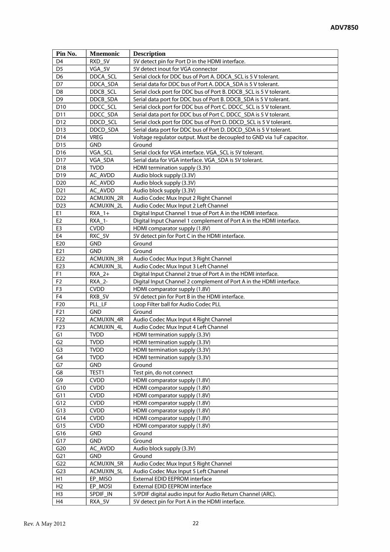
ADV7850
Rev. A May 2012 22
Pin No. Mnemonic Description D4 RXD_5V 5V detect pin for Port D in the HDMI interface. D5 VGA_5V 5V detect inout for VGA connector D6 DDCA_SCL Serial clock for DDC bus of Port A. DDCA_SCL is 5 V tolerant. D7 DDCA_SDA Serial data for DDC bus of Port A. DDCA_SDA is 5 V tolerant. D8 DDCB_SCL Serial clock port for DDC bus of Port B. DDCB_SCL is 5 V tolerant. D9 DDCB_SDA Serial data port for DDC bus of Port B. DDCB_SDA is 5 V tolerant. D10 DDCC_SCL Serial clock port for DDC bus of Port C. DDCC_SCL is 5 V tolerant. D11 DDCC_SDA Serial data port for DDC bus of Port C. DDCC_SDA is 5 V tolerant. D12 DDCD_SCL Serial clock port for DDC bus of Port D. DDCD_SCL is 5 V tolerant. D13 DDCD_SDA Serial data port for DDC bus of Port D. DDCD_SDA is 5 V tolerant. D14 VREG Voltage regulator output. Must be decoupled to GND via 1uF capacitor. D15 GND Ground D16 VGA_SCL Serial clock for VGA interface. VGA_SCL is 5V tolerant. D17 VGA_SDA Serial data for VGA interface. VGA_SDA is 5V tolerant. D18 TVDD HDMI termination supply (3.3V) D19 AC_AVDD Audio block supply (3.3V) D20 AC_AVDD Audio block supply (3.3V) D21 AC_AVDD Audio block supply (3.3V) D22 ACMUXIN_2R Audio Codec Mux Input 2 Right Channel D23 ACMUXIN_2L Audio Codec Mux Input 2 Left Channel E1 RXA_1+ Digital Input Channel 1 true of Port A in the HDMI interface. E2 RXA_1- Digital Input Channel 1 complement of Port A in the HDMI interface. E3 CVDD HDMI comparator supply (1.8V) E4 RXC_5V 5V detect pin for Port C in the HDMI interface. E20 GND Ground E21 GND Ground E22 ACMUXIN_3R Audio Codec Mux Input 3 Right Channel E23 ACMUXIN_3L Audio Codec Mux Input 3 Left Channel F1 RXA_2+ Digital Input Channel 2 true of Port A in the HDMI interface. F2 RXA_2- Digital Input Channel 2 complement of Port A in the HDMI interface. F3 CVDD HDMI comparator supply (1.8V) F4 RXB_5V 5V detect pin for Port B in the HDMI interface. F20 PLL_LF Loop Filter ball for Audio Codec PLL F21 GND Ground F22 ACMUXIN_4R Audio Codec Mux Input 4 Right Channel F23 ACMUXIN_4L Audio Codec Mux Input 4 Left Channel G1 TVDD HDMI termination supply (3.3V) G2 TVDD HDMI termination supply (3.3V) G3 TVDD HDMI termination supply (3.3V) G4 TVDD HDMI termination supply (3.3V) G7 GND Ground G8 TEST1 Test pin, do not connect G9 CVDD HDMI comparator supply (1.8V) G10 CVDD HDMI comparator supply (1.8V) G11 CVDD HDMI comparator supply (1.8V) G12 CVDD HDMI comparator supply (1.8V) G13 CVDD HDMI comparator supply (1.8V) G14 CVDD HDMI comparator supply (1.8V) G15 CVDD HDMI comparator supply (1.8V) G16 GND Ground G17 GND Ground G20 AC_AVDD Audio block supply (3.3V) G21 GND Ground G22 ACMUXIN_5R Audio Codec Mux Input 5 Right Channel G23 ACMUXIN_5L Audio Codec Mux Input 5 Left Channel H1 EP_MISO External EDID EEPROM interface H2 EP_MOSI External EDID EEPROM interface H3 SPDIF_IN S/PDIF digital audio input for Audio Return Channel (ARC). H4 RXA_5V 5V detect pin for Port A in the HDMI interface.

ADV7850
Rev. A May 2012 23
Pin No. Mnemonic Description H7 GND Ground H8 GND Ground H9 GND Ground H10 GND Ground H11 GND Ground H12 GND Ground H13 GND Ground H14 GND Ground H15 GND Ground H16 GND Ground H17 GND Ground H20 GND Ground H21 GND Ground H22 FILTA Audio Codec ADC filter capacitor H23 VREF_AUDIO Audio Codec block reference voltage capacitor J1 EP_CSB External EDID EEPROM interface J2 EP_SCK External EDID EEPROM interface J3 SHARED_EDID EDID selection signal for HDMI Port D J4 RESET Chip Reset. Active low. Minimum low time guarantee reset is 5 msec. J7 GND Ground J8 GND Ground J9 GND Ground J10 GND Ground J11 GND Ground J12 GND Ground J13 GND Ground J14 GND Ground J15 GND Ground J16 GND Ground J17 GND Ground J20 AC_AVDD Audio block supply (3.3V) J21 GND Ground J22 ISET Audio Codec ADC current settings J23 FILTD Audio Codec DAC filter capacitor K1 GND Ground K2 GND Ground K3 DVDDIO I/O supply (3.3V) K4 DVDDIO I/O supply (3.3V) K7 VDD Video Digital supply (1.8V) K8 GND Ground K9 GND Ground K10 GND Ground K11 GND Ground K12 GND Ground K13 GND Ground K14 GND Ground K15 GND Ground K16 GND Ground K17 GND Ground K20 AC_AVDD Audio block supply (3.3V) K21 AC_AVDD Audio block supply (3.3V) K22 AC_DACOut_R Audio Codec DAC output right channel K23 AC_DACOut_L Audio Codec DAC output left channel L1 HA_AP5 HDMI Audio port output L2 HA_SCLK HDMI Audio port serial clock output. L3 INT1 External Interrupt 1. L4 SDA I2C port serial data input/output pin. L7 VDD Video Digital supply (1.8V) L8 GND Ground

ADV7850
Rev. A May 2012 24
Pin No. Mnemonic Description L9 GND Ground L10 GND Ground L11 GND Ground L12 GND Ground L13 GND Ground L14 GND Ground L15 GND Ground L16 GND Ground L17 GND Ground L20 AC_AVDD Audio block supply (3.3V) L21 AC_AVDD Audio block supply (3.3V) L22 HPOUT_R Headphone output right channel L23 HPOUT_L Headphone output left channel M1 HA_AP4 HDMI Audio port output M2 HA_AP3/INT3 HDMI Audio port output or External Interrupt pin 3. This pin can be configured as
a TTL output interrupt pin for the VDP SPI interface. M3 INT2 External Interrupt 2. M4 SCL I2C port serial clock input. M7 VDD Video Digital supply (1.8V) M8 GND Ground M9 GND Ground M10 GND Ground M11 GND Ground M12 GND Ground M13 GND Ground M14 GND Ground M15 GND Ground M16 GND Ground M17 GND Ground M20 AC_AVDD Audio block supply (3.3V) M21 GND Ground M22 GND Ground M23 GND Ground N1 HA_AP2 HDMI Audio port output N2 HA_AP1 HDMI Audio port output N3 AC_MCLK Audio Codec/DAC clock input N4 AC_LRCLK Audio DAC Left/Right clock input N7 VDD Video Digital supply (1.8V) N8 GND Ground N9 GND Ground N10 GND Ground N11 GND Ground N12 GND Ground N13 GND Ground N14 GND Ground N15 GND Ground N16 GND Ground N17 GND Ground N20 PVDD DPLL supply (1.8V) N21 PVDD DPLL supply (1.8V) N22 XTALN Xtal output N23 XTALP Xtal input or external clock input P1 HA_AP0 HDMI Audio port output P2 HA_MCLKOUT HDMI Audio master clock output P3 AC_SDI Audio DAC data input P4 AC_SCLK Audio DAC SCLK input P7 VDD Video Digital supply (1.8V) P8 GND Ground P9 GND Ground

ADV7850
Rev. A May 2012 25
Pin No. Mnemonic Description P10 GND Ground P11 GND Ground P12 GND Ground P13 GND Ground P14 GND Ground P15 GND Ground P16 GND Ground P17 GND Ground P20 GND Ground P21 GND Ground P22 GND Ground P23 GND Ground R1 TTX_SCLK VBI data interface R2 TTX_MOSI VBI data interface R3 TTX_MISO VBI data interface R4 TTX_CSB VBI data interface R7 VDD Video Digital supply (1.8V) R8 GND Ground R9 GND Ground R10 GND Ground R11 GND Ground R12 GND Ground R13 GND Ground R14 GND Ground R15 GND Ground R16 GND Ground R17 GND Ground R20 GND Ground R21 GND Ground R22 REFN Analog video reference output R23 REFP Analog video reference output T1 DVDDIO I/O supply (3.3V) T2 DVDDIO I/O supply (3.3V) T3 GND Ground T4 GND Ground T7 VDD Video Digital supply (1.8V) T8 GND Ground T9 GND Ground T10 GND Ground T11 GND Ground T12 GND Ground T13 GND Ground T14 GND Ground T15 GND Ground T16 GND Ground T17 GND Ground T20 AVDD Video Analog supply voltage (1.8V) T21 AVDD Video Analog supply voltage (1.8V) T22 AVDD Video Analog supply voltage (1.8V) T23 AVDD Video Analog supply voltage (1.8V) U1 TX_AVDD HDMI Tx Analog Supply (1.8V) U2 TX_AVDD HDMI Tx Analog Supply (1.8V) U3 GND Ground U4 TX_DDC_SCL Serial clock for DDC bus of HDMI Tx. TX_DDCA_SCL is 5 V tolerant. U7 VDD Video Digital supply (1.8V) U8 VDD Video Digital supply (1.8V) U9 VDD Video Digital supply (1.8V) U10 VDD Video Digital supply (1.8V) U11 VDD Video Digital supply (1.8V)

ADV7850
Rev. A May 2012 26
Pin No. Mnemonic Description U12 VDD Video Digital supply (1.8V) U13 VDD Video Digital supply (1.8V) U14 TEST2 Test pin, do not connect U15 GND Ground U16 GND Ground U17 GND Ground U20 AVIN13 Analog video mux input channel U21 AVIN12 Analog video mux input channel U22 AVIN11 Analog video mux input channel U23 AVIN10 Analog video mux input channel V1 TX_2+ Digital Output Channel 2 true of the HDMI Tx. V2 TX_2- Digital Output Channel 2 complement of the HDMI Tx. V3 GND Ground V4 TX_DDC_SDA Serial data for DDC bus of HDMI Tx. TX_DDCA_SDA is 5 V tolerant. V20 AVDD Video Analog supply voltage (1.8V) V21 AVDD Video Analog supply voltage (1.8V) V22 AVDD Video Analog supply voltage (1.8V) V23 AVDD Video Analog supply voltage (1.8V) W1 TX_1+ Digital Output Channel 1 true of the HDMI Tx. W2 TX_1- Digital Output Channel 1 complement of the HDMI Tx. W3 GND Ground W4 TX_HPD Hot Plug Detect signal of the HDMI Tx. W20 GND Ground W21 AVOUT2 Analog Video Mux output 2 W22 AVIN9 Analog video mux input channel W23 AVIN8 Analog video mux input channel Y1 TX_0+ Digital Output Channel 0 true of the HDMI Tx. Y2 TX_0- Digital Output Channel 0 complement of the HDMI Tx. Y3 GND Ground Y4 GND Ground Y5 A7 SDRAM address line Y6 A3 SDRAM address line Y7 A10 SDRAM address line Y8 BA0 SDRAM block address signal Y9 CKE SDRAM clock enable Y10 GND Ground Y11 DQ6 SDRAM data line Y12 DQ7 SDRAM data line Y13 DQ0 SDRAM data line Y14 DQ8 SDRAM data line Y15 UDQS SDRAM upper data strobe true signal Y16 SDVDD Memory interface supply Y17 SAVDD SDRAM interface supply Y18 TRI1 Digital input capable of slicing bi-level or tri-level input from SCART or D-
Connector. Y19 TRI2 Digital input capable of slicing bi-level or tri-level input from SCART or D-
Connector. Y20 GND Ground Y21 AVOUT1 Analog Video Mux output 1 Y22 SYNC3 This is a synchronization on green or luma input (SOG/SOY) used in embedded
synchronization mode. Y23 AVIN7 Analog video mux input channel AA1 TX_C+ Digital Output clock true of the HDMI Tx. AA2 TX_C- Digital Output clock complement of the HDMI Tx. AA3 TX_AVDD HDMI Tx Analog Supply (1.8V) AA4 GND Ground AA5 A9 SDRAM address line AA6 A5 SDRAM address line AA7 A1 SDRAM address line

ADV7850
Rev. A May 2012 27
Pin No. Mnemonic Description AA8 BA1 SDRAM block address signal AA9 WE SDRAM write enable signal AA10 GND Ground AA11 DQ4 SDRAM data line AA12 DQ5 SDRAM data line AA13 DQ2 SDRAM data line AA14 DQ11 SDRAM data line AA15 UDQSN SDRAM upper data strobe compliment signal AA16 SDVDD Memory interface supply AA17 GND Ground AA18 HS_IN1/TRI7 HSync on Graphics Port. The HSync input signal is used for 5-wire timing mode.
This ball can also be used as a trilevel/bilevel input on the SCART or D-terminal connector.
AA19 VS_IN1/TRI8 VS on Graphics Port. The VS input signal is used for 5-wire timing mode. This ball can also be used as a trilevel/bilevel input on the SCART or D-terminal connector.
AA20 GND Ground AA21 TRI3 Digital input capable of slicing bi-level or tri-level input from SCART or D-
Connector. AA22 HS_IN2/TRI5 The HSync input signal is used for 5-wire timing mode. This ball can also be used
as a trilevel/bilevel input on the SCART or D-terminal connector. AA23 VS_IN2/TRI6 The VS input signal is used for 5-wire timing mode. This ball can also be used as a
trilevel/bilevel input on the SCART or D-terminal connector. AB1 GND Ground AB2 TX_PVDD HDMI Tx digital supply (1.8V) AB3 TX_PLVDD HDMI Tx PLL digital supply (1.8V). It is important to ensure that this supply pin has
a clean voltage input. AB4 SDVDD Memory interface supply AB5 A11 SDRAM address line AB6 A6 SDRAM address line AB7 A2 SDRAM address line AB8 CAS SDRAM interface Column Address Select Command Signal. One of four command
signals to the external SDRAM. AB9 RAS SDRAM interface Row Address Select Command Signal. One of four command
signals to the external SDRAM. AB10 VREF Termination reference voltage for memory interface AB11 SDVDD Memory interface supply AB12 LDQSN SDRAM lower data strobe compliment signal AB13 DQ3 SDRAM data line AB14 DQ10 SDRAM data line AB15 DQ12 SDRAM data line AB16 DQ14 SDRAM data line AB17 GND Ground AB18 SYNC1 This is a synchronization on green or luma input (SOG/SOY) used in embedded
synchronization mode. AB19 AVIN3 Analog video mux input channel AB20 GND Ground AB21 SYNC2 This is a synchronization on green or luma input (SOG/SOY) used in embedded
synchronization mode. AB22 AVIN6 Analog video mux input channel AB23 TRI4 Digital input capable of slicing bi-level or tri-level input from SCART or D-
Connector. AC1 GND Ground AC2 TX_RTERM This signal sets the internal termination resistance. A 470R resistor between this
ball and GND should be used. AC3 TX_VDD33 HDMI Tx PLL Regulator Supply input (3.3V). This pin is an internal voltage
regulator input. AC4 SDVDD Memory interface supply AC5 A8 SDRAM address line AC6 A4 SDRAM address line AC7 A0 SDRAM address line

ADV7850
Rev. A May 2012 28
Pin No. Mnemonic Description AC8 CS SDRAM interface Chip Select. SDRAM CS Enables and disables the command
decoder on the RAM. One of four command signals to the external SDRAM. AC9 CKN SDRAM interface Differential Clock Compliment Output. All address and control
output signals to the RAM should be sampled on the positive edge of CK and on the negative edge of CKN.
AC10 CK SDRAM interface Differential Clock Right Output. All address and control output signals to the RAM should be sampled on the positive edge of CK and on the negative edge of CKN.
AC11 SDVDD Memory interface supply AC12 LDQS SDRAM lower data strobe true signal AC13 DQ1 SDRAM data line AC14 DQ9 SDRAM data line AC15 DQ15 SDRAM data line AC16 DQ13 SDRAM data line AC17 GND Ground AC18 AVIN1 Analog video mux input channel AC19 AVIN2 Analog video mux input channel AC20 GND Ground AC21 AVIN4 Analog video mux input channel AC22 AVIN5 Analog video mux input channel AC23 GND Ground

ADV7850
Rev. A May 2012 29
3 GLOBAL CONTROL REGISTERS
The control bits described in this section deal with the general control of the chip and the three main sections of the ADV7850: the SDP, the CP, and the HDMI receiver.
3.1 ADV7850 REVISION IDENTIFICATION rd_info[15:0], IO, Address 0xE1[7:0]; Address 0xE2[7:0] (Read Only) This readback displays the chip revision code.
Function rd_info[15:0] Description 0x2101 Version Number
3.2 POWER-DOWN CONTROLS
3.2.1 Primary Power-down Controls power_down is the main power-down control. It is the main control for power-down for the HDMI Rx, SDP, VDP and CP sections power_down, IO, Address 0x0C[5] This control is used to enable power-down mode. This is the main I2C power-down control.
Function power_down Description 0 Chip operational 1 Enable chip power down
tx_power_down, Addr B8 (Main), Address 0x41[6] Tx power down.
Function tx_power_down Description 0 Normal operation 1 << HDMI Tx power down
3.2.2 Secondary Power-down Controls The cp_pwrdn, xtal_pdn, core_pdn, and vdp_pdn controls allow various sections of the ADV7850 to be powered down. For a power-sensitive application, it is possible to stop the clock to the CP to reduce power. cp_pwrdn enables this power-save mode. The SDP, VDP, and HDMI blocks are not affected by this power-save mode. This allows the use of limited HDMI, SSPD, and STDI monitoring features while reducing the power consumption. For full processing of HDMI input the CP core needs to be powered up. xtal_pdn allows the user to power down the XTAL clock in the following sections:
• STDI blocks • SSPD blocks • Free run synchronization generation block • I2C sequencer block, which is used for the configuration of the gain, clamp, and offset • CP and HDMI sections • Frequency measurement block, and its derivatives, for example, frequency settings for equalizers

ADV7850
Rev. A May 2012 30
• DDC pads (active pull-up depends on XTAL) • Reset
The XTAL clock is also provided to the HDCP engine, EDID, and the repeater controller within the HDMI receiver. The XTAL clock within these sections is not affected by xtal_pdn. core_pdn allows the user to power down clocks, with the exception of the XTAL clock, in the following sections:
• CP block • SDP block • Digital section of the HDMI block
The following sections remain active when core_pdn is set:
• STDI block • SSPD block
cp_pwrdn, Addr A0 (VFE), Address 0x0C[2] This control is used to power down the clock to the CP core.
Function cp_pwrdn Description 0 Power up clock to CP core. 1 Power down clock to CP core. VDP, DPP and HDMI blocks not affected.
xtal_pdn, IO, Address 0x0B[0] This control is used to power down the xtal in the digital blocks.
Function xtal_pdn Description 0 Power up xtal buffer to digital core 1 Power down xtal buffer to digital core
core_pdn, IO, Address 0x0B[1] This control is used to power down the DPP, CP core and digital sections of the HDMI core.
Function core_pdn Description 0 Power up DPP, CP, SDP and digital sections of HDMI block. 1 Power down DPP, CP, SDP and digital sections of HDMI block. STDI and SSPD still active when
core_pdn set. vdp_pdn, Addr A0 (VFE), Address 0x0C[1] This control is used to power down the VDP. It is recommended to power down the VDP when this feature is not required.
Function vdp_pdn Description 0 Power up VDP section 1 Power down VDP section
3.2.3 Power-down Mode The ADV7850 supports the following power-down modes.
• In power-down mode 1, selected sections and pads are kept active to provide E-EDID and +5 V antiglitch filter functionality.
ADV7850
Rev. A May 2012 31
• In power-down mode 0, all the sections of the ADV7850 are disabled except for the following blocks: I2C slave section E-EDID/Repeater controller E-EDID ring oscillator
The ring oscillator provides a clock to the E-EDID/Repeater controller (refer to Section 7.4) and the +5 V power supply antiglitch filter. The clock output from the ring oscillator runs approximately at 50 MHz.
The following are the only pads enabled in power-down mode:
• I2C pads: SDA SCL
• +5 V pads: RXA_5V RXB_5V RXC_5V RXD_5V HPA_A HPA_B HPA_C HPA_D
• DDC pads: DDCA_SCL DDCA_SDA DDCB_SCL DDCB_SDA DDCC_SCL DDCC_SDA DDCD_SCL DDCD_SDA
• SPI EEPROM interface pads: EP_MOSI EP_MISO EP_CS EP_SCK
• Reset pad : RESET
Entering Power-down Mode The ADV7850 can be put into power-down mode 0 via the software as follows:
• Set power_down to 1 • Set tx_power_down to 1
Leaving Power-down Mode 0 via Software The ADV7850 can be removed from power-down mode via the software as follows:
• Set power_down to 0 • Set tx_power_down to 0
3.2.4 EDID Support in Power-off Mode The ADV7850 fully supports EDID read functionality in a powered off configuration. The 5V signal from the HDMI or graphic cable can be used to power the EDID controller on the ADV7850. Onboard regulators will provide a 3.3V signal to power the SPI EEPROM. The following configuration can be used to provide EDID functionality when in a powered off state. If this feature is not used on the ADV7850 the VDD_EEPROM pin must be decoupled through a 100nF capacitor to ground.

ADV7850
Rev. A May 2012 32
Figure 4: Required Hardware Configuration When Using +5 V from HDMI Source(s) to Provide EDID Support in Powered Off State
3.2.5 ADC Power-down Control The ADV7850 contains 12-bit ADCs (ADC 0, ADC 1, ADC 2, and ADC3). It is possible to power down each ADC individually, if required. pdn_adc0, AFE, Address 0x00[0] This control is used to power down ADC0.
Function pdn_adc0 Description 0 Power up 1 Power down
pdn_adc1, AFE, Address 0x00[1] This control is used to power down ADC1.
Function pdn_adc1 Description 0 Power up 1 Power down
pdn_adc2, AFE, Address 0x00[2] This control is used to power down ADC2.
Function pdn_adc2 Description 0 Power up 1 Power down
pdn_adc3, AFE, Address 0x00[3] This control is used to power down ADC3.
H D M IP ort D
H D M IP ort C
H D M IP ort B
P ort A
+ 5 V
+ 5 V
+ 5 V
+ 5 V
4SPI interface
RXD_5VRXC_5VRXB_5VRXA_5V
A D V 7850
S P IE E P R O M
(8 k b it)
VGAPort
H D M I
H D M I
VGA _5V
VDD_EEPROM
+ 5 V
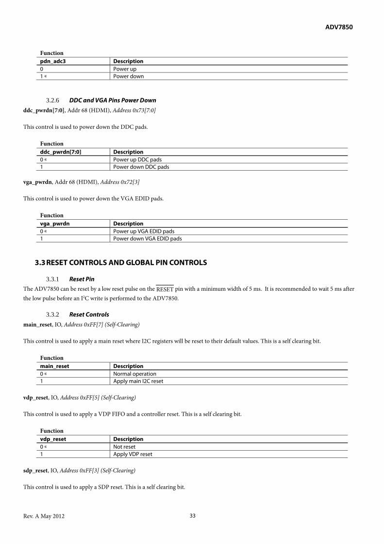
ADV7850
Rev. A May 2012 33
Function pdn_adc3 Description 0 Power up 1 Power down
3.2.6 DDC and VGA Pins Power Down ddc_pwrdn[7:0], Addr 68 (HDMI), Address 0x73[7:0] This control is used to power down the DDC pads.
Function
ddc_pwrdn[7:0] Description 0 Power up DDC pads 1 Power down DDC pads
vga_pwrdn, Addr 68 (HDMI), Address 0x72[3] This control is used to power down the VGA EDID pads.
Function vga_pwrdn Description 0 Power up VGA EDID pads 1 Power down VGA EDID pads
3.3 RESET CONTROLS AND GLOBAL PIN CONTROLS
3.3.1 Reset Pin The ADV7850 can be reset by a low reset pulse on the RESET pin with a minimum width of 5 ms. It is recommended to wait 5 ms after the low pulse before an I2C write is performed to the ADV7850.
3.3.2 Reset Controls main_reset, IO, Address 0xFF[7] (Self-Clearing) This control is used to apply a main reset where I2C registers will be reset to their default values. This is a self clearing bit.
Function main_reset Description 0 Normal operation 1 Apply main I2C reset
vdp_reset, IO, Address 0xFF[5] (Self-Clearing) This control is used to apply a VDP FIFO and a controller reset. This is a self clearing bit.
Function vdp_reset Description 0 Not reset 1 Apply VDP reset
sdp_reset, IO, Address 0xFF[3] (Self-Clearing) This control is used to apply a SDP reset. This is a self clearing bit.

ADV7850
Rev. A May 2012 34
Function sdp_reset Description 0 Not reset 1 Apply SDP reset
sdp_mem_reset, IO, Address 0xFF[2] (Self-Clearing) This control is used to apply a memory interface reset. This is a self clearing bit.
Function sdp_mem_reset Description 0 Not reset 1 Apply SDP memory reset
tx_soft_reset, IO, Address 0x1B[7] (Self-Clearing) This control is used for software reset of the HDMI Tx. This is a self clearing bit.
Function tx_soft_reset Description 1 Software reset to Tx block
3.3.3 Tristate Pins tri_audio, IO, Address 0x15[4] (Self-Clearing) This control is used to apply a memory interface reset. This is a self clearing bit.
Function TRI_AUDIO Description 0 << Audio output pins active 1 Tristate audio output pins
3.3.4 ADC Phase Control dll_phase[5:0], Addr 4C (DPLL), Address 0xC8[5:0] This control is used to adjust the phase of the ADC clocks in CP modes.
Function dll_phase[5:0] Description 000000 << Default xxxxxx Adjust phase of clock in CP modes
3.4 ADC-HDMI SIMULTANEOUS MODE The ADV7850 can be configured to be in either simultaneous mode or non simultaneous mode, as follows:
• Simultaneous mode In this mode, specific subsections of the HDMI block remain enabled when the ADV7850 is programmed to process analog inputs through the CP and SD core. Simultaneous mode keeps the HDCP engine and the E-EDID/Repeater controller active, allowing an upstream transmitter to authenticate the ADV7850 even when the latter is in analog mode. Keeping the HDCP engine active allows for fast switching from analog mode to HDMI mode, as the transmitter will have already authenticated the ADV7850 when the latter is switched into HDMI mode. Simultaneous mode is also used for SDP and HDMI audio mode (refer to Section 4.2.)
ADV7850
Rev. A May 2012 35
• Non simultaneous mode In this mode, the ADV7850 processes either analog or HDMI/DVI inputs. The HDMI section is disabled when the ADV7850 is configured to process analog inputs. The ADCs are powered down when the part is configured to process HDMI/DVI inputs in HDMI mode.
Notes:
• Simultaneous mode has no effect when the part is programmed in HDMI mode as the full HDMI section is enabled in this mode
• The ADCs are powered down automatically in HDMI mode, with the exception of simultaneous CVBS and HDMI audio mode, as mentioned previously
• The following HDMI subsections are active and functional when the ADV7850 runs in simultaneous mode: TMDS equalizer (refer to Section 7.13 ) TMDS clock detection circuitry (refer to Section 7.16) TMDS clock measurement circuitry (refer to Section 7.17) HDCP decryption engine (refer to Section 7.21) HDMI synchronization filters (refer to Section 7.24) InfoFrame and packet extraction processor (refer to Section 7.34)
• The following HDMI subsections are active and functional irrespective of the simultaneous mode: 5 V deglitch filter and detection circuitry (refer to Section 7.1) E-EDID/Repeater controller (refer to Section 7.4)
adc_hdmi_simult_mode, IO, Address 0x01[7] This control is used to enable ADC and HDMI simultaneous mode. In this mode, certain HDMI functionality is available when processing analog inputs.
Function adc_hdmi_simult_mode Description 0 Disable simultaneous mode 1 Enable simultaneous mode
hdcp_only_mode, Addr 68 (HDMI), Address 0x00[6] This control is used to configure a HDCP only mode for simultaneous analog and HDMI modes. Refer to the adc_hdmi_simultaneous_mode bit. By selecting HDCP only mode, HDMI activity is reduced and it can be used as a power saving feature in simultaneous analog and HDMI operation.
Function hdcp_only_mode Description 0 Normal operation 1 HDCP only mode

ADV7850
Rev. A May 2012 36
4 PRIMARY MODE AND VIDEO STANDARD
Setting the primary mode and choosing a video standard are the most fundamental settings when configuring the ADV7850. There are four main modes of operation on the ADV7850. These modes are enabled by setting prim_mode[3:0] appropriately.
• SDP mode Analog-composite and analog S-Video mode. This covers all standard definition modes that have a modulated color subcarrier. Typical examples are PAL-BGHID, PAL-M/N, NTSC-M/N and SECAM. SDP also supports SD YPrPb and SD SCART RGB. The SDP core is the main processing block in this mode.
• Component mode Analog-component video mode. This includes all video signals that arrive in a YPbPr (or YUV) analog format. Typical examples are progressive and high definition video signals. The CP core is the main processing block in this mode.
• Graphics mode Analog-graphic mode. This mode is intended for RGB input signals with high bandwidth. The CP core is the main processing block in this mode.
• HDMI mode HDMI mode. In HDMI mode the ADV7850 can receive and decode HDMI or DVI data throughout the DVI/HDMI receiver front end. Video data from the HDMI receiver is routed to the HDMI Tx while audio data is available on the audio interface. This mode is enabled by selecting either the HDMI Graphics primary mode or HDMI Component primary mode.
4.1 PRIMARY MODE AND VIDEO STANDARD CONTROLS prim_mode[3:0], Addr A0 (VFE), Address 0x01[3:0] This control is used to select the primary mode of operation of the decoder. It is to be used with vid_std[5:0].
Function prim_mode[3:0] Description 0000 SDP mode 0001 Component mode 0010 Graphics mode 0011 Reserved 0100 Reserved 0101 HDMI-Comp 0110 HDMI-GR 0111 - 1111 Reserved
vid_std[5:0], Addr A0 (VFE), Address 0x00[5:0] This control is used to set the input video standards and oversampling mode. Its configuration is dependent on prim_mode[3:0].
Function vid_std[5:0] Description 000010 Default
prim_mode[3:0] should be used with vid_std[5:0] to set the desired video mode. Both controls should be set according to Table 2. For HDMI modes vid_std[5:0] can be left at default.
Table 2: Primary Mode and Video Standard Selection prim_mode[3:0] vid_std[5:0]
Code Description Processor Code Input Video Output Resolution Comment
0000 SDP (Standard Definition)
SDP 00000 SD 2x1 720x480i/576i CVBS 00001 SD 4x1 720x480i/576i CVBS
00010 Reserved Reserved

ADV7850
Rev. A May 2012 37
prim_mode[3:0] vid_std[5:0]
Code Description Processor Code Input Video Output Resolution Comment e.g. CVBS
00011 Reserved Reserved
00100 SD 2x1 720x480i/576i SCART RGB 00101 SD 4x1 720x480i/576i SCART RGB
00110 Reserved Reserved 00111 Reserved Reserved
01000 SD 2x1 720x480i/576i YC 01001 SD 4x1 720x480i/576i YC
01010 SD 8x1 720x480i/576i YC 01011 Reserved Reserved
01100 SD 2x1 720x480i/576i YC auto 01101 SD 4x1 720x480i/576i YC auto
01110 Reserved Reserved 01111 Reserved Reserved
11111 Reserved Reserved 10000 SD 2X1 YPrPb 720X480i/576i SD Component
10001 SD 4X1 YPrPb 720X480i/576i SD Component 10010 Reserved Reserved
10011 Reserved Reserved 10100 Reserved Reserved
10101 Reserved Reserved 10110 Reserved Reserved
10111 Reserved Reserved 11000 SD 2x1 RGB 720x480i/576i SD Component
11001 SD 4x1 RGB 720x480i/576i SD Component 11010 Reserved Reserved
11110 Reserved Reserved 11111 Reserved Reserved
0001
COMP (Component Video) e.g. YPrPb
000000 Reserved Reserved 000001 Reserved Reserved
000010 SD 2x1 525i 720 x 480i 000011 SD 2x1 625i 720 x 576i
000100 SD 4x1 525i 720 x 480i 000101 SD 4x1 625i 720 x 576i
000110 SD 2x2 525i 1440 x 480i 000111 SD 2x2 625i 1440 x 576i
CP 001000 SD 4x2 525i 1440 x 480i 001001 SD 4x2 625i 1440 x 576i
001010 Reserved Reserved 001011 Reserved Reserved
001100 PR 2x1 525p 720 x 480p 001101 PR 2x1 625p 720 x 576p
001110 PR 4x1 525p 720 x 480p 001111 PR 4x1 625p 720 x 576p
010000 PR 2x2 525p 1440 x 480p 010001 PR 2x2 625p 1440 x 576p
010010 Reserved Reserved 010011 HD 1x1 720p 1280 x 720p SMPTE 296M
010100 HD 1x1 1125 1920 x 1080i SMPTE 274M 010101 HD 1x1 1125 1920 x 1035i SMPTE 240M

ADV7850
Rev. A May 2012 38
prim_mode[3:0] vid_std[5:0]
Code Description Processor Code Input Video Output Resolution Comment
010110 HD 1x1 1250 1920 x 1080i SMPTE 295M
010111 HD 1x1 1250 1920 x 1152i 011000 Reserved Reserved
011001 HD 2x1 720p 1280 x 720p SMPTE 296M 011010 HD 2x1 1125 1920 x 1080i SMPTE 274M
011011 HD 2x1 1125 1920 x 1035i SMPTE 240M 011100 HD 2x1 1250 1920 x 1080i SMPTE 295M
011101 HD 2x1 1250 1920 x 1152i
011110 HD 1x1 1125p 1920 x 1080p SMPTE 274M
011111 HD 1x1 1250p 1920 x 1080p SMPTE 295M
~ Reserved Reserved
~ Reserved Reserved
111110 HD 1x1 1125p 1920 x 1080p Reduced blanking
111111 Reserved Reserved
0010
GR (Graphics) e.g. RGB
000000 SVGA 800 x 600p @ 56
000001 SVGA 800 x 600p @ 60 000010 SVGA 800 x 600p @ 72
000011 SVGA 800 x 600p @ 75 000100 SVGA 800 x 600p @ 85
000101 SXGA 1280 x 1024p @ 60 000110 SXGA 1280 x 1024p @ 75
000111 Auto-graphics Mode Various
001000 VGA 640 x 480p @ 60 001001 VGA 640 x 480p @ 72
001010 VGA 640 x 480p @ 75 001011 VGA 640 x 480p @ 85
CP 001100 XGA 1024 x 768p @ 60 001101 XGA 1024 x 768p @ 70
001110 XGA 1024 x 768p @ 75 001111 XGA 1024 x 768p @ 85
010000 WXGA 1280 x768p @ 60
010001 WXGA 1280 x768p @ 60 With reduced blanking
010010 WXGA 1360 x768p @ 60
010011 WXGA 1366 x768p @ 60
010100 SXGA+ 1400x1050p @ 60
010101 SXGA+ 1400x1050p @ 75
010110 UXGA 1600x1200p @ 60
010111 UXGAR 1600x1200p @ 60 With reduced blanking
011000 WSXGA 1680x1050p @ 60
011001 WUXGAR 1920x1200p @ 60 With reduced blanking
~ Reserved Reserved
111111 Reserved Reserved 0011 Reserved xxxxx Reserved Reserved
0100 SDP + HDMI Audio SD + CP
000000 SD 2x1 720 x 480i/576i CVBS 000001 Reserved Reserved
000010 Reserved Reserved 000011 Reserved Reserved
000100 Reserved Reserved

ADV7850
Rev. A May 2012 39
prim_mode[3:0] vid_std[5:0]
Code Description Processor Code Input Video Output Resolution Comment 000101 Reserved Reserved
000110 Reserved Reserved 000111 Reserved Reserved
001000 SD 2x1 YUV 720x480i/576i YC 001001 Reserved Reserved
001010 SD 2x1 RGB 720x480i/576i YPrPb ~ Reserved Reserved
111111 Reserved Reserved
0101
HDMI-COMP (Component Video)
CP 000000 SD 1x1 525i 720 x 480i
HDMI Non-Mux mode
000001 SD 1x1 625i 720 x 576i 000010 SD 2x1 525i 720 x 480i
CP 000011 SD 2x1 625i 720 x 576i CP 000100 Reserved Reserved
CP 000101 Reserved Reserved CP 000110 Reserved Reserved
000111 Reserved Reserved CP 001000 Reserved Reserved
CP 001001 Reserved Reserved CP 001010 PR 1x1 525p 720 x 480p
CP 001011 PR 1x1 625p 720 x 576p CP 001100 PR 2x1 525p 720 x 480p
CP 001101 PR 2x1 625p 720 x 576p CP 001110 Reserved Reserved
CP 001111 Reserved Reserved 010000 Reserved Reserved
010001 Reserved Reserved 010010 Reserved Reserved
CP 010011 HD 1x1 1280 x 720p CP 010100 HD 1x1 1920 x 1080i
CP 010101 HD 1x1 1920 x 1035 CP 010110 HD 1x1 1920 x 1080
CP 010111 HD 1x1 1920 x 1152 011000 Reserved Reserved
CP 011001 HD 2x1 720p 1280 x 720p CP 011010 HD 2x1 1125i 1920 x 1080i
CP 011011 HD 2x1 1125 1920 x 1035 CP 011100 HD 2x1 1250 1920 x 1080
CP 011101 HD 2x1 1250 1920 x 1152 CP 011110 HD 1x1 1920 x 1080p
CP 011111 HD 1x1 1920 x 1080
0110
HDMI-GR Graphics)
CP 000000 SVGA 800 x 600p @ 56
HDMI Non-Mux Mode
CP 000001 SVGA 800 x 600p @ 60 CP 000010 SVGA 800 x 600p @ 72
CP 000011 SVGA 800 x 600p @ 75 CP 000100 SVGA 800 x 600p @ 85
CP 000101 SXGA 1280 x 1024p @ 60 CP 000110 SXGA 1280 x 1024p @ 75
000111 Reserved Reserved CP 001000 VGA 640 x 480p @ 60

ADV7850
Rev. A May 2012 40
prim_mode[3:0] vid_std[5:0]
Code Description Processor Code Input Video Output Resolution Comment CP 001001 VGA 640 x 480p @ 72
CP 001010 VGA 640 x 480p @ 75 CP 001011 VGA 640 x 480p @ 85
CP 001100 XGA 1024 x 768p @ 60 CP 001101 XGA 1024 x 768p @ 70
CP 001110 XGA 1024 x 768p @ 75 CP 001111 XGA 1024 x 768p @ 85
01xxxx Reserved 0111 Reserved xxxxxx Reserved Reserved
4.1.1 Setting the Vertical Frequency v_freq[2:0] is used when the decoder is required to support HD standards SMPTE 274, systems 6, 7, 8, 9, 10, and 11; and SMPTE 296, systems 3, 4, 5, and 6. These are the 50 Hz, 30 Hz, and 24 Hz standards listed within these standards. This control should be set when the primary mode is configured for component mode. The primary mode is set by the prim_mode[3:0] control. Table 3 details the vertical frequencies supported by the ADV7850 for various resolutions. v_freq[2:0], Addr A0 (VFE), Address 0x01[6:4] This control is used to set the vertical frequency of HD component standards.
Function v_freq[2:0] Description 000 60 Hz 001 50 Hz 010 30 Hz 011 25 Hz 100 24 Hz 101 Reserved 110 Reserved 111 Reserved
Table 3: Vertical Frequencies Supported in HD Modes Standard SM296
720p 1x1
BT709 1035i 1x1
SM274 1080i 1x1
SM295 1250i 1x1
BT709 1250i 1x1
SM274 1080p 1x1
SM295 1250p 1x1
Vertical Frequency ↓ (Hz)
SM274-1,2 SM274-3 SM274-7,8 SM274-9 SM274-10, 11
4.2 STANDARD CONFIGURATION FOR SDP-HDMI AUDIO SIMULTANEOUS MODE CVBS video can be processed simultaneously with HDMI audio. In this configuration, CVBS is only supported in 2x1 oversampling mode. This mode is available for S-Video and 525i and 625i SD modes. This mode can be selected by the relevant prim_mode[3:0] and vid_std[5:0]. Frame TBC and 3D comb are not available in this mode. When switching into this mode it is recommended to mute the audio as the changing modes may cause a disturbance to the audio output. To configure the ADV7850 for this mode, the following I2C writes should be carried out:

ADV7850
Rev. A May 2012 41
• Primary mode should be configured for SDP and HDMI audio mode (prim_mode[3:0] set to 0x04) • ADC simultaneous mode should be enabled (adc_hdmi_simult_mode set to 0x01). • The desired 2x1 SDP mode should be configured by setting vid_std[5:0]
2x1 CVBS (vid_std[5:0] set to 0x00) 2x1 YC (vid_std[5:0] set to 0x08) 2x1 YPrPb (vid_std[5:0] set to 0x10)
• Select Clocking mode for Audio to the output. IO Map Register 0xD9 to a value of 0x09. This configures the mode to CVBS + HDMI Audio. IO Map Register 0xD8 to a value of 0x10. This enables the manual clocking mode
4.3 PRIMARY MODE AND VIDEO STANDARD CONFIGURATION FOR HDMI FREE RUN To support Free run in HDMI Mode, the ADV7850 must use the CP core. Free Run is only supported up to 225MHz. If free run is enabled in HDMI mode, PRIM_MODE [3:0] and VID_STD [5:0] should be used to specify the output resolution to which the ADV7850 free runs. Along with specifying the standard to free run to from the HDMI Non-Mux mode standards, DIS_AUTO_PARAM_BUFFER should be set to 1 also.

ADV7850
Rev. A May 2012 42
5 ANALOG FRONT END
The analog front end (AFE) comprises the following: • High performance 12-bit analog to digital converters (ADCs) with clamping circuitry • Thirteen analog inputs and multiplexing capability • Three synchronization (SYNC1, SYNC2 and SYNC3) input multiplexers with synchronization slicers and filtering • Variable bandwidth anti aliasing filters • LLC-DLL (Line Locked Clock – Delay Locked Loop) • Eight trilevel input detection blocks
5.1 ADC SAMPLING CLOCK The ADV7850 has two main modes of operation for sampling the input analog video: CP mode and SDP mode. This is determined by the primary mode setting.
• When the SDP is enabled, fixed 108 MHz sampling is applied to the ADCs. The SDP processes the video signal and, using a line length tracking processor, resamples the incoming video so that 720 active pixels are always generated per line. Note that no user I2C settings are available for the PLL when in SDP mode as the PLL is controlled directly by the SDP.
• When the CP is enabled, true line locked sampling is applied to the video signal being processed. This means that the horizontal synchronization signal of the incoming video signal is applied to the PLL and multiplied by the desired number of samples per line, which yields the pixel sampling clock used in CP mode.
The CP ADC sampling clock is a line locked clock that is generated automatically by a digital encoder synthesizer. The following controls enable the user to adjust the ADC sampling clock: pll_div_man_en, Addr A0 (VFE), Address 0x16[7] This control is used to manually override the PLL divider ratio value.
Function pll_div_man_en Description 0 Disable manual PLL divider ratio settings. PLL divider ratio set by prim_mode[3:0] and
vid_std[5:0]. 1 Set pll_div_ratio manually as defined by pll_div[12:0].
pll_div_ratio[12:0], Addr A0 (VFE), Address 0x16[4:0]; Address 0x17[7:0] This control is used to set the manual PLL divide ratio. It is sequenced and requires sequential writes for the desired value to be updated.
Function pll_div_ratio[12:0] Description xxxxxxxxxxxxx Synthesizer feedback value. pll_man_val_en must be set for this value to be active.
5.2 ADCS AND VOLTAGE CLAMPS
5.2.1 Analog Input Hardware Configuration The ADV7850 supports 13 analog inputs. The analog inputs have an input range of 0 to 1 V.
Figure 5: Analog Inputs Hardware Configuration

ADV7850
Rev. A May 2012 43
5.2.2 Clamp Operation The ADV7850 has a clamp in front of each of its ADCs. The purpose of the clamp is to ensure that the video input signal lies inside the range of the ADC. In component and graphics modes, voltage clamps are used; and in standard definition modes, current clamps are used. Clamping is done automatically and does not require user programming. Optimum performance is selected by default. Figure 5 shows the resistor divider network required on each analog input to scale the input video to the input range of the ADCs.
Figure 6: Video Input Signal Level Prior to 24 Ohm to 51 Ohm Resistor Divider
Figure 7: Video Input Signal Level After Voltage Clamps
5.2.3 SDP Clamp Operation Standard definition video signals can have excessive noise on them; especially CVBS signals transmitted by terrestrial broadcast and demodulated using a tuner. These usually show very large levels of noise. A voltage clamp would be unsuitable for this type of video signal. Instead, the ADV7850 employs a set of current sources that can cause currents to flow into and away from the high impedance node that carries the video signal (refer to Figure 8). Since the input video is AC coupled into the ADV7850, its DC value needs to be restored. This process is referred to as clamping the video. This section explains the general process of clamping on the ADV7850 for the SDP and shows the different ways in which a user can configure its behavior. The SDP block uses a combination of current sources and a digital processing block for clamping, as shown in Figure 8.
730mV
1.345 V
0.615 V
~0.5V 980mV
Clamp Level
1.345 V
0.615 V
~0.5V 730mV
830mV Clamp Level
Y Signal Range
~1V
Pr/Pb Input Signal Range 1.6V
1.6V
~1V
Y Input Signal Range
Pr/Pb Signal Range

ADV7850
Rev. A May 2012 44
Figure 8: SDP Clamping Overview
The clamping can be divided into two sections:
• Clamping before the ADC (analog domain): digitally controlled current sources • Clamping after the ADC (digital domain): digital processing block
The ADCs can digitize an input signal if it resides within the ADC input voltage range of 1.0 V. An input signal with a DC level that is too large or too small will be clipped at the top or bottom of the ADC range. The primary task of the analog clamping circuits is to ensure that the video signal stays within the valid ADC input window so that the analog-to-digital conversion can take place. After digitization, the digital fine clamp block corrects for any remaining variations in DC level. Since the DC level of an input video signal refers directly to the brightness of the picture transmitted, it is important to perform a fine clamp with high accuracy, otherwise brightness variations can occur. This section describes the I2C signals used to influence the behavior of the SDP clamping. sdp_dclp_speed[4:0], Addr 90 (SDP), Address 0x0C[4:0] This control is used to adjust the speed of digital clamp operation.
Function sdp_dclp_speed[4:0] Description 00000 Freeze digital clamp Valid range 1 to 6 All other values Reserved
sdp_dclp_speed[4:0] determines the time constant of the digital clamp circuitry. It is important to realize that the digital clamp reacts very fast to correct immediately any residual DC level error for the active line. The time constant of the digital clamp must be a lot faster than the one from the analog blocks. This register also allows the user to freeze the digital clamp loop at any point in time. By default, the time constant of the digital clamp is adjusted dynamically to suit the currently connected input signal. sdp_aclp_speed[4:0], Addr 90 (SDP), Address 0x0D[4:0] This control is used to adjust the speed of the analog clamp operation.
Function sdp_aclp_speed[4:0] Description 00000 Freeze analog clamp Valid range 1 to 6 All other values Reserved
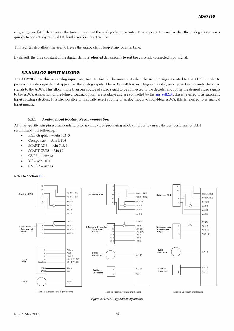
ADV7850
Rev. A May 2012 45
sdp_aclp_speed[4:0] determines the time constant of the analog clamp circuitry. It is important to realize that the analog clamp reacts quickly to correct any residual DC level error for the active line. This register also allows the user to freeze the analog clamp loop at any point in time. By default, the time constant of the digital clamp is adjusted dynamically to suit the currently connected input signal.
5.3 ANALOG INPUT MUXING The ADV7850 has thirteen analog input pins, Ain1 to Ain13. The user must select the Ain pin signals routed to the ADC in order to process the video signals that appear on the analog inputs. The ADV7850 has an integrated analog muxing section to route the video signals to the ADCs. This allows more than one source of video signal to be connected to the decoder and routes the desired video signals to the ADCs. A selection of predefined routing options are available and are controlled by the ain_sel[2:0]; this is referred to as automatic input muxing selection. It is also possible to manually select routing of analog inputs to individual ADCs; this is referred to as manual input muxing.
5.3.1 Analog Input Routing Recommendation ADI has specific Ain pin recommendations for specific video processing modes in order to ensure the best performance. ADI recommends the following:
• RGB Graphics − Ain 1, 2, 3 • Component − Ain 4, 5, 6 • SCART RGB − Ain 7, 8, 9 • SCART CVBS – Ain 10 • CVBS 1 – Ain12 • YC – Ain 10, 11 • CVBS 2 – Ain13
Refer to Section 15.
Figure 9: ADV7850 Typical Configurations

ADV7850
Rev. A May 2012 46
5.4 AUTOMATIC INPUT MUXING SELECTION By selecting the various ain_sel[2:0] values, the user can direct the predefined analog input to ADC routing options. The AIN_SEL also controls the routing of embedded synchronization on the SYNC pins to the embedded synchronization slicers. Embedded synchronization refers to a synchronization signal that is ‘embedded’ in the input video signal itself, for example, Sync on Green (SOG) and Sync on Y (SOY) type signals. Note that CVBS, YC and SD components have to be manually routed using adc0_sw_man[3:0], adc1_sw_man[3:0], adc2_sw_man[3:0], and adc3_sw_man[3:0] while adc_switch_man is set to 1. (Refer to Section 5.5.1.)
Figure 10: ADV7850 Input Functional Diagram
ain_sel[2:0], AFE, Address 0x02[2:0] This control is used to select the analog input muxing mode.
ADV7850
Rev. A May 2012 47
Function ain_sel[2:0] Description Code ADC0|ADC1|ADC2|ADC3|EMB_SYNC_SEL1|EMB_SYNC_SEL2 000 NC | Ain1 | Ain2 | Ain3 | Sync1 | Sync2 001 NC | Ain4 | Ain5 | Ain6 | Sync2 | Sync1 010 Ain10 | Ain7 | Ain8 | Ain9 |
The emb_sync_sel_1 signal should be considered as the main synchronization input for this muxing arrangement, and the emb_sync_sel_2 signal will be monitored in parallel through the second synchronization stripper.
5.5 MANUAL INPUT MUXING OVERVIEW By accessing a set of manual override muxing registers, the analog input muxes of the ADV7850 can be controlled directly. This is referred to as manual input muxing (refer to Section 5.5.1). Notes:
• Manual input muxing overrides all other input muxing control bits, for example, ain_sel[2:0]. The manual muxing is activated by setting the adc_switch_man. It only affects the analog switches in front of the ADCs. prim_mode[3:0] and vid_std[5:0] still have to be set so the follow on blocks process the video data in the correct format.
• Manual input muxing only controls the analog input muxes. • The ADI recommended input combinations are designed to minimize crosstalk between input channels. When using the
manual input muxing, special care must be taken by the user/PCB designer to take care of cross coupling.
Not every input pin can be routed to any ADC. There are restrictions in the channel routing imposed by the analog signal routing inside the IC (refer to Section 5.5.1).
5.5.1 Manual Input Muxing The manual muxing controls listed in this section configure the analog inputs. These controls should be used to override the auto configuration described in Section 5.4. Note: The following rules must be adhered to when selecting analog input routing to the ADCs:
• CVBS signals must always connect to ADC0. • Y/C signals must always connect to ADC0 and ADC1. Y must connect to ADC0 and C must connect to ADC1. • YPrPb signals must always connect to ADC1, ADC2 and ADC3. Y must connect to ADC1, Pr must connect to ADC2 and Pb
must connect to ADC3. • RGB signals must always connect to ADC1, ADC2 and ADC3. G must connect to ADC1, R must connect to ADC2 and B must
connect to ADC3. Refer to Table 5 for more information. adc_switch_man, AFE, Address 0x02[7] This control is used to enable manual input muxing to the ADCs.
Function adc_switch_man Description 0 Automatic muxing 1 Manual muxing
Once adc_switch_man is set to 1, the following controls take effect.
ADV7850
Rev. A May 2012 48
adc0_sw_man[3:0], AFE, Address 0x03[7:4] This control is used to manually route analog inputs to ADC0.
Function adc0_sw_man[3:0] Description 0101 Ain5 1010 Ain10 1011 Ain11 1100 Ain12 1101 Ain13 All others Reserved
adc1_sw_man[3:0], AFE, Address 0x03[3:0] This control is used to manually route analog inputs to ADC 1.
Function adc1_sw_man[3:0] Description 0001 Ain1 0100 Ain4 0111 Ain7 1011 Ain11 All others Reserved
adc2_sw_man[3:0], AFE, Address 0x04[7:4] This control is used to manually route analog inputs to ADC2.
Function adc2_sw_man[3:0] Description 0010 Ain2 0101 Ain5 1000 Ain8 1011 Ain11 All others Reserved
adc3_sw_man[3:0], AFE, Address 0x04[3:0] This control is used to manually route analog inputs to ADC3.
Function adc3_sw_man[3:0] Description 0011 Ain3 0110 Ain6 1001 Ain9 All others Reserved
Table 4: Manual Input Muxing
adc0_sw_man[3:0] adc1_sw_man[3:0] adc2_sw_man[3:0] adc3_sw_man[3:0]
ADC0 Connected to
ADC1 Connected to
ADC2 Connected to
ADC3 Connected to
0000 - - - - 0001 - AIN1 - - 0010 - - AIN2 - 0011 - - - AIN3 0100 - AIN4 - -

ADV7850
Rev. A May 2012 49
adc0_sw_man[3:0] adc1_sw_man[3:0] adc2_sw_man[3:0] adc3_sw_man[3:0]
ADC0 Connected to
ADC1 Connected to
ADC2 Connected to
ADC3 Connected to
0101 AIN5 - AIN5 - 0110 - - - AIN6 0111 - AIN7 - - 1000 - - AIN8 - 1001 - - - AIN9 1010 AIN10 - - - 1011 AIN11 AIN11 AIN11 AIN11 1100 AIN12 - - - 1101 AIN13 - - - 1110 - - - - 1111 - - - -
ADC Mapping
Table 5: Recommended Video Signal to ADC Routing Mode Required ADC
Mapping ADI Recommended Ain Channel
CVBS CVBS = ADC0 CVBS = Ain 12 YC/YC auto Y = ADC0
C = ADC1 Y= Ain 10 C = Ain11
SCART RGB1 CVBS = ADC0 G = ADC1 B = ADC3 R = ADC2
CVBS = Ain 10 G = Ain 7 B = Ain 9 R = Ain 8
CP YPrPb Y = ADC1 Pr = ADC2 Pb = ADC3
G = Ain 4 R = Ain 5 B = Ain 6
Graphics RGB G = ADC1 B = ADC3 R = ADC2
G = Ain 1 R = Ain 2 B = Ain 3
5.6 VIDEO OUTPUT MUX The input mux also has the capability to multiplex a predefined list of analog inputs onto AOUT, as shown in Table 6.
Table 6: Available Inputs on Aout1 and Aout2 Aout Available Inputs 1 Ain5, Ain10, Ain11, Ain12, Ain13 2 Ain4, Ain11, Ain12
vout1_sel[3:0], AFE, Address 0x2C[3:0] This control is used to switch analog inputs to Vout1.
Function vout1_sel[3:0] Description 0101 Ain5 1010 Ain10 1011 Ain11 1100 Ain12 1101 Ain13 All others Reserved

ADV7850
Rev. A May 2012 50
vout2_sel[3:0], AFE, Address 0x2C[7:4] This control is used to switch analog inputs to Vout2.
Function vout2_sel[3:0] Description 0100 Ain4 1011 Ain11 1100 Ain12 All others Reserved
aout1_clamp_en, AFE, Address 0x2E[5] This control is used to set the clamping on AOUT1.
Function aout1_clamp_en Description 0 Disable Clamping on AOUT1 1 Enable Resistor Clamping on AOUT1
aout2_clamp_en, AFE, Address 0x2E[4] This control is used to set the clamping on AOUT2.
Function aout2_clamp_en Description 0 Disable Clamping on AOUT2 1 Enable Resistor Clamping on AOUT2
5.7 SYNC1-3 INPUT CONTROL As shown in Figure 11, the ADV7850 has three input synchronization control pins: SYNC1, SYNC2 and SYNC3. These pins are used for signals with embedded synchronization, for example, SOG or SOY type signals. SOG is associated with RGB input video; SOY is associated with component YPrPb input video. These synchronization inputs can be muxed to two synchronization strippers also in the AFE. From here, the signals are routed to synchronization processors in the CP. This muxing can be performed in an automatic configuration mode or with manual control. These are described in Sections 5.7.1 and 5.7.2 respectively.

ADV7850
Rev. A May 2012 51
Figure 11: Synchronization Stripper Circuit
5.7.1 Automatic Synchronization Configuration In addition to configuring the analog input muxes, ain_sel[2:0]controls automatically the associated synchronization channel routing. Refer to Figure 9 and the ain_sel[2:0] description for the routing details when ain_sel[2:0] is programmed.
5.7.2 Manual Synchronization Configuration Figure 10 shows the input synchronization muxes, which can be controlled manually as well as automatically. Manual control is enabled via emb_sync_sel_man_en; and emb_sync_1_sel_man[1:0] and emb_sync_2_sel_man[1:0] select the SYNC source for each embedded sync processor. This section describes the control bits for manual operation. emb_sync_sel_man_en, AFE, Address 0x02[6] This control is used to enable manual selection of embedded synchronization inputs to synchronization strippers. In automatic mode, ain_sel[3:0] makes the selection. In manual mode, emb_sync_1_selman[1:0] and emb_sync_2_selman[1:0] makes the selection.
Function emb_sync_sel_man_en Description 0 Automatic sync selection 1 Manual sync selection
emb_sync_1_sel_man[1:0], AFE, Address 0x15[7:6] This control is used to select a manual embedded synchronization for emb_sync1.

ADV7850
Rev. A May 2012 52
Function emb_sync_1_sel_man[1:0]
Description
00 Sync1 pin 01 Sync2 pin 10 Sync3 pin 11 Reserved
emb_sync_2_sel_man[1:0], AFE, Address 0x15[5:4] This control is used to select a manual embedded synchronization for emb_sync2.
Function emb_sync_2_sel_man[1:0]
Description
00 Sync1 pin 01 Sync2 pin 10 Sync3 pin 11 Reserved
5.8 SYNCHRONIZATION SLICERS The ADV7850 has two synchronization slicer blocks, which are placed before the synchronization processing sections, as shown in Figure 10. The purpose of a synchronization slicer is to provide a reliable synchronization signal to the STDI and SSPD circuits in the component processor so that a robust identification of standard is made. A second synchronization slicer is provided to allow processing of a second or, possibly, a third channel. A more in depth picture of Sync Slicer 1 is shown in Figure 11. The circuit is duplicated for Sync Slicer 2.
5.8.1 Synchronization Filter Stage There are two synchronization strippers in the ADV7850 similar to that shown in Figure 11. Any of the three SYNC pins; SYNC 1, SYNC 2, and SYNC 3 can be routed to the filter stage. sync1_filter_sel[1:0], AFE, Address 0x15[3:2] This control is used to select the clamp filter on sync channel 1.
Function sync1_filter_sel[1:0] Description 00 No filter 01 Sync > 250 ns 10 Sync > 1 us 11 Sync > 2.5 us
sync2_filter_sel[1:0], AFE, Address 0x15[1:0] This control is used to select the clamp filter on sync channel 2.
Function sync2_filter_sel[1:0] Description 00 No filter 01 Sync > 250 ns 10 Sync > 1 us 11 Sync > 2.5 us

ADV7850
Rev. A May 2012 53
5.8.2 Sync Stripper Slice Level A comparator stage is located after the filter stage. This has programmable thresholds, which offer the user various slice levels that determine the presence of a valid synchronization pulse. The register slice_level[4:0] is a 5-bit register that sets up slice levels for both Sync Stripper 1 and Sync Stripper 2. slice_level[4:0], AFE, Address 0x16[4:0] This control is used to set the slice level in the synchronization strippers. A smaller value corresponds to a higher slice level. For a clamp at 300 mV, the slice level is equal to 600 mV - ((slice_level + 1) * 9.375 mV).
Function slice_level[4:0] Description 00000 Highest slice level XXXXX Clamp at 300 mV and slice at 600 mV - ((XXXXX + 1) * 9.375 mV) 11000 Default 11111 Lowest slice level
Several video connectors and cables have signals that are structured as three-level signals. These include the European SCART connector, which has two such signals; and the Japanese D-connector, which has three. These signals convey much information about the parameters of the signal being sent. In order for the ADV7850 to use this information, it must slice the voltage levels appearing on TRI1-TRI8. The following eight pins are capable of slicing a trilevel signal in the ADV7850:
• TRI1 • TRI2 • TRI3 • TRI4 • HS_IN1/TRI5 (known also as TRI5) • VS_IN2/TRI6 (known also as TRI6) • HS_IN2/TRI7 (known also as TRI7) • VS_IN2/TRI8 (known also as TRI8)
5.8.3 D-Terminal Connector Table 7 and Table 8 show details of the D-terminal connector used in Japan. The Dataline 1, Dataline 2, and Dataline 3 signals are the three signals that can be applied to any of the eight TRI inputs. The ADV7850 can process two D-terminal connectors. In this case, six of the available eight TRI inputs would be utilized.
Table 7: D-Terminal Connector Characteristics (Trilevel) Level Minimum
Voltage Maximum Voltage
Pin 8 (Dataline 1) Pin 11 (Dataline 3)
A 0 V 0 V 525 lines 4:3 B 1.4 V 2.4 V 750 lines 4:3 letterbox C 3.5 V 5 V 1125 lines 16:9
Table 8: D-Terminal Connector Characteristics (Bilevel)
Level Typical Voltage Pin 9 (Dataline 2) A 0 V 59.94i/60i B 5 V 59.94p/60p
5.8.4 TRI 1-8 Input Resistor Selection As can be seen from Table 7, Table 8, Table 9, and Table 10, the voltage levels to be sliced exceed the power supplies of the ADV7850 and, therefore, are beyond the range of the ADV7850 TRI inputs. The applied signals need to be reduced to fit in the range of the slicers. This is done by utilizing resistor divider networks at the inputs to TRI1-8.

ADV7850
Rev. A May 2012 54
The recommended resistor values for voltages related to the D-terminal and SCART connectors are shown in Figure 12.
Figure 12: D-Terminal Resistor Dividers
5.8.5 Trilevel Input Controls The ADV7850 has eight trilevel slicers, as shown in Figure 13. Each trilevel slicer is capable of operating in two modes. The first mode is bilevel mode where the input signal can be sliced at a single voltage level to determine the voltage level (refer to Table 8). The second mode is trilevel mode. This mode can be used to determine the voltage level of the trilevel signals present from inputs such as D-terminal connectors. All levels are programmable. The outputs from these slicers are available via readback registers. The output from these slicers are also sent to a digital processor in the AFE that generates a system interrupt if any inputs to the TRI 1-8 pins change state. All interrupts can be enabled and serviced via I2C. Note that a trilevel input pin may also be configured as a fast blank control pin for SCART functionality.
Figure 13: Trilevel Slicer
5.8.6 Trilevel Slicer Operation Each trilevel slicer can be powered up or down.

ADV7850
Rev. A May 2012 55
tri1_slicer_pwrdn, AFE, Address 0x1D[6] This control is used to power down the Tri1 slicer.
Function tri1_slicer_pwrdn Description 0 Power up 1 Power down
tri2_slicer_pwrdn, AFE, Address 0x1E[6] This control is used to power down the Tri2 slicer.
Function tri2_slicer_pwrdn Description 0 Power up 1 Power down
tri3_slicer_pwrdn, AFE, Address 0x1F[6] This control is used to power down the Tri3 slicer.
Function tri3_slicer_pwrdn Description 0 Power up 1 Power down
tri4_slicer_pwrdn, AFE, Address 0x20[6] This control is used to power down the Tri4 slicer.
Function tri4_slicer_pwrdn Description 0 Power up 1 Power down
tri5_slicer_pwrdn, AFE, Address 0x21[6] This control is used to power down the Tri5 slicer.
Function tri5_slicer_pwrdn Description 0 Power up 1 Power down
tri6_slicer_pwrdn, AFE, Address 0x22[6] This control is used to power down the Tri6 slicer.
Function tri6_slicer_pwrdn Description 0 Power up 1 Power down

ADV7850
Rev. A May 2012 56
tri7_slicer_pwrdn, AFE, Address 0x23[6] This control is used to power down the Tri7 slicer.
Function tri7_slicer_pwrdn Description 0 Power up 1 Power down
tri8_slicer_pwrdn, AFE, Address 0x24[6] This control is used to power down the Tri8 slicer.
Function tri8_slicer_pwrdn Description 0 Power up 1 Power down
5.8.7 Bilevel/Trilevel Selection Each slicer operates in trilevel slice mode by default. The following controls are used to switch between bilevel mode and trilevel mode. tri1_bilevel_slice_en, AFE, Address 0x1D[5] This control is used to enable bilevel slicing on the Tri1 input.
Function tri1_bilevel_slice_en Description 0 Bilevel slicing 1 Trilevel slicing
tri2_bilevel_slice_en, AFE, Address 0x1E[5] This control is used to enable bilevel slicing on the Tri2 input.
Function tri2_bilevel_slice_en Description 0 Bilevel slicing 1 Trilevel slicing
tri3_bilevel_slice_en, AFE, Address 0x1F[5] This control is used to enable bilevel slicing on the Tri3 input.
Function tri3_bilevel_slice_en Description 0 Bilevel slicing 1 Trilevel slicing
tri4_bilevel_slice_en, AFE, Address 0x20[5] This control is used to enable bilevel slicing on the Tri4 input.

ADV7850
Rev. A May 2012 57
Function tri4_bilevel_slice_en Description 0 Bilevel slicing 1 Trilevel slicing
tri5_bilevel_slice_en, AFE, Address 0x21[5] This control is used to enable bilevel slicing on the Tri5 input.
Function tri5_bilevel_slice_en Description 0 Bilevel slicing 1 Trilevel slicing
tri6_bilevel_slice_en, AFE, Address 0x22[5] This control is used to enable bilevel slicing on the Tri6 input.
Function tri6_bilevel_slice_en Description 0 Bilevel slicing 1 Trilevel slicing
tri7_bilevel_slice_en, AFE, Address 0x23[5] This control is used to enable bilevel slicing on the Tri7 input.
Function tri7_bilevel_slice_en Description 0 Bilevel slicing 1 Trilevel slicing
tri8_bilevel_slice_en, AFE, Address 0x24[5] This control is used to enable bilevel slicing on the Tri8 input.
Function tri8_bilevel_slice_en Description 0 Bilevel slicing 1 Trilevel slicing
5.8.8 Trilevel Slicer Readbacks The input has two comparators on it for each trilevel slicer (refer to Figure 13).The raw results of these comparators are available via the trix_readback[1:0] registers. ‘Upper level’ in the following descriptions refers to trix_upper_slice_level (where x is 1 to 8). ‘Lower level’ refers to trix_lower_slice_level (where x is 1 to 8). tri1_readback[1:0], AFE, Address 0x27[7:6] (Read Only) This readback displays Tri1 DC levels.
ADV7850
Rev. A May 2012 58
Function tri1_readback[1:0] Description 1x Signal higher than upper level 0x Signal lower than upper level x1 Signal higher than lower level x0 Signal lower than lower level
tri2_readback[1:0], AFE, Address 0x27[5:4] (Read Only) This readback displays Tri2 DC levels.
Function tri2_readback[1:0] Description 1x Signal higher than upper level 0x Signal lower than upper level x1 Signal higher than lower level x0 Signal lower than lower level
tri3_readback[1:0], AFE, Address 0x27[3:2] (Read Only) This readback displays Tri3 DC levels.
Function tri3_readback[1:0] Description 1x Signal higher than upper level 0x Signal lower than upper level x1 Signal higher than lower level x0 Signal lower than lower level
tri4_readback[1:0], AFE, Address 0x27[1:0] (Read Only) This readback displays Tri4 DC levels.
Function tri4_readback[1:0] Description 1x Signal higher than upper level 0x Signal lower than upper level x1 Signal higher than lower level x0 Signal lower than lower level
tri5_readback[1:0], AFE, Address 0x28[7:6] (Read Only) This readback displays Tri5 DC levels.
Function tri5_readback[1:0] Description 1x Signal higher than upper level 0x Signal lower than upper level x1 Signal higher than lower level x0 Signal lower than lower level
tri6_readback[1:0], AFE, Address 0x28[5:4] (Read Only) This readback displays Tri6 DC levels.

ADV7850
Rev. A May 2012 59
Function tri6_readback[1:0] Description 1x Signal higher than upper level 0x Signal lower than upper level x1 Signal higher than lower level x0 Signal lower than lower level
tri7_readback[1:0], AFE, Address 0x28[3:2] (Read Only) This readback displays Tri7 DC levels.
Function tri7_readback[1:0] Description 1x Signal higher than upper level 0x Signal lower than upper level x1 Signal higher than lower level x0 Signal lower than lower level
tri8_readback[1:0], AFE, Address 0x28[1:0] (Read Only) This readback displays Tri8 DC levels.
Function tri8_readback[1:0] Description 1x Signal higher than upper level 0x Signal lower than upper level x1 Signal higher than lower level x0 Signal lower than lower level
5.8.9 Programming Trilevel Slicers When the slicers are in a bilevel mode of operation (refer to Section 5.8.7), the upper slicer is utilized. This offers the programmability described in Section 5.8.9.1. When any of the trilevel slicer circuits are in trilevel mode (refer to Section 5.8.7), the upper levels (UL) are sliced by the upper_slicer, as described in Section 5.8.9.1. The lower levels are sliced by the lower_slicer (LL), as described in Section 5.8.9.2).
5.8.9.1 Upper Slice Levels
tri1_upper_slice_level[2:0], AFE, Address 0x1D[4:2] This control is used to set the upper slice level on the Tri1 input.
Function tri1_upper_slice_level[2:0]
Description
000 75 mV 001 225 mV 010 375 mV 011 525 mV 100 675 mV 101 825 mV 110 975 mV 111 1.125 V
tri2_upper_slice_level[2:0], AFE, Address 0x1E[4:2] This control is used to set the upper slice level on the Tri2 input.
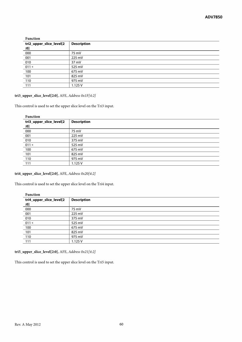
ADV7850
Rev. A May 2012 60
Function tri2_upper_slice_level[2:0]
Description
000 75 mV 001 225 mV 010 37 mV 011 525 mV 100 675 mV 101 825 mV 110 975 mV 111 1.125 V
tri3_upper_slice_level[2:0], AFE, Address 0x1F[4:2] This control is used to set the upper slice level on the Tri3 input.
Function tri3_upper_slice_level[2:0]
Description
000 75 mV 001 225 mV 010 375 mV 011 525 mV 100 675 mV 101 825 mV 110 975 mV 111 1.125 V
tri4_upper_slice_level[2:0], AFE, Address 0x20[4:2] This control is used to set the upper slice level on the Tri4 input.
Function tri4_upper_slice_level[2:0]
Description
000 75 mV 001 225 mV 010 375 mV 011 525 mV 100 675 mV 101 825 mV 110 975 mV 111 1.125 V
tri5_upper_slice_level[2:0], AFE, Address 0x21[4:2] This control is used to set the upper slice level on the Tri5 input.

ADV7850
Rev. A May 2012 61
Function tri5_upper_slice_level[2:0]
Description
000 75 mV 001 225 mV 010 375 mV 011 525 mV 100 675 mV 101 825 mV 110 975 mV 111 1.125 V
tri6_upper_slice_level[2:0], AFE, Address 0x22[4:2] This control is used to set the upper slice level on the Tri6 input.
Function tri6_upper_slice_level[2:0]
Description
000 75 mV 001 225 mV 010 375 mV 011 525 mV 100 675 mV 101 825 mV 110 975 mV 111 1.125 V
tri7_upper_slice_level[2:0], AFE, Address 0x23[4:2] This control is used to set the upper slice level on the Tri7 input.
Function tri7_upper_slice_level[2:0]
Description
000 75 mV 001 225 mV 010 375 mV 011 525 mV 100 675 mV 101 825 mV 110 975 mV 111 1.125 V
tri8_upper_slice_level[2:0], AFE, Address 0x24[4:2] This control is used to set the upper slice level on the Tri8 input.
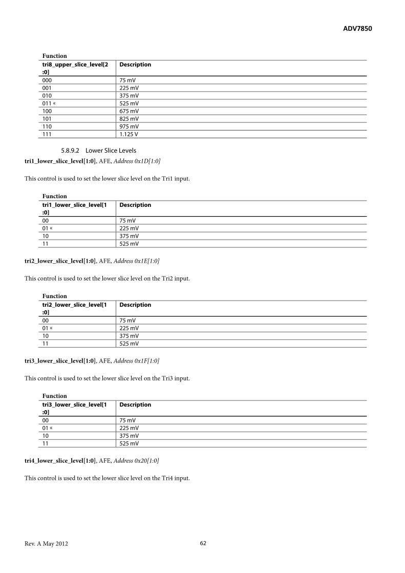
ADV7850
Rev. A May 2012 62
Function tri8_upper_slice_level[2:0]
Description
000 75 mV 001 225 mV 010 375 mV 011 525 mV 100 675 mV 101 825 mV 110 975 mV 111 1.125 V
5.8.9.2 Lower Slice Levels
tri1_lower_slice_level[1:0], AFE, Address 0x1D[1:0] This control is used to set the lower slice level on the Tri1 input.
Function tri1_lower_slice_level[1:0]
Description
00 75 mV 01 225 mV 10 375 mV 11 525 mV
tri2_lower_slice_level[1:0], AFE, Address 0x1E[1:0] This control is used to set the lower slice level on the Tri2 input.
Function tri2_lower_slice_level[1:0]
Description
00 75 mV 01 225 mV 10 375 mV 11 525 mV
tri3_lower_slice_level[1:0], AFE, Address 0x1F[1:0] This control is used to set the lower slice level on the Tri3 input.
Function tri3_lower_slice_level[1:0]
Description
00 75 mV 01 225 mV 10 375 mV 11 525 mV
tri4_lower_slice_level[1:0], AFE, Address 0x20[1:0] This control is used to set the lower slice level on the Tri4 input.

ADV7850
Rev. A May 2012 63
Function tri4_lower_slice_level[1:0]
Description
00 75 mV 01 225 mV 10 375 mV 11 525 mV
tri5_lower_slice_level[1:0], AFE, Address 0x21[1:0] This control is used to set the lower slice level on the Tri5 input.
Function tri5_lower_slice_level[1:0]
Description
00 75 mV 01 225 mV 10 375 mV 11 525 mV
tri6_lower_slice_level[1:0], AFE, Address 0x22[1:0] This control is used to set the lower slice level on the Tri6 input.
Function tri6_lower_slice_level[1:0]
Description
00 75 mV 01 225 mV 10 375 mV 11 525 mV
tri7_lower_slice_level[1:0], AFE, Address 0x23[1:0] This control is used to set the lower slice level on the Tri7 input.
Function tri7_lower_slice_level[1:0]
Description
00 75 mV 01 225 mV 10 375 mV 11 525 mV
tri8_lower_slice_level[1:0], AFE, Address 0x24[1:0] This control is used to set the lower slice level on the Tri8 input.
Function tri8_lower_slice_level[1:0]
Description
00 75 mV 01 225 mV 10 375 mV 11 525 mV
The ADV7850 can support simultaneous processing of CVBS and RGB standard definition signals to enable SCART compatibility and

ADV7850
Rev. A May 2012 64
overlay functionality. This is a standard definition mode and is enabled by prim_mode[3:0] and vid_std[5:0]controls. In this mode, timing extraction is always performed by the SDP on the CVBS signal. However, a combination of the CVBS and RGB video inputs can be mixed and output on the pixel port. The video selection is under the control of I2C registers or a fast blank signal applied to one of the trilevel inputs. (The trilevel input is selected using fb_select[3:0].) By default, the ADV7850 operates in a dynamic switching mode in which the source selection is under the control of the fast blank signal. This enables dynamic multiplexing between the CVBS and RGB sources. When the fast blank signal is logic HI, the RGB source is selected; when the fast blank signal is logic LO, the CVBS source is selected. This is suitable for the overlay of subtitles, teletext, and so on. Typically, the CVBS source carries the main picture and the RGB source has the overlay data. The source selection can also be controlled manually via the I2C registers. Manual source selection mode is enabled using sdp_man_fb_en. In manual mode, either the CVBS content or the RGB content can be output under the control of sdp_man_fb. This mode allows the selection of a full screen picture from either source. Overlay is not possible in manual mode. fb_select[3:0], AFE, Address 0x14[3:0] This control is used to select the trilevel input to use as fast blank.
Function fb_select[3:0] Description 0000 TRI1 0001 TRI2 0010 TRI3 0011 TRI4 0100 TRI5/HS_IN2 0101 TRI6/VS_IN2 0110 TRI7/HS_IN1 0111 TRI8/VS_IN1 1xxx Reserved
5.8.10 Fast Blanking Configuration A block diagram of the ADV7850 fast blanking configuration is shown in Figure 14.
Figure 14: ADV7850 Fast Blanking Configuration The CVBS signal is processed by the SDP and converted to YPbPr. The RGB signals are also processed by the SDP and are converted to YPbPr. Both sets of YPbPr signals are input to the subpixel blender, which can be configured to operate manually using sdp_man_fb control or dynamically using the fast blank input signal.
A D C 0
A D C 1 A D C 2 A D C 3
GREEN RED BLUE
C V B S S I G N A L C O N D I T I O N I N G C L A M P I N G A N D
D E C I M A T I O N
T I M I N G E X T R A C T I O N
S I G N A L C O N D I T I O N I N G C L A M P I N G A N D
D E C I M A T I O N
V I D E O P R O C E S S I N G
R G B T O Y P r P b
C O N V E R S I O N
Y P r P b S U B P I X E L B L E N D E R
O U T P U T F O R M A T T E R
F A S T B L A N K P O S I T I O N
R E S O L V E R F A S T B L A N K S I G N A L
S D P

ADV7850
Rev. A May 2012 65
The fast blank position resolver determines the time position of the fast blank to a very high accuracy and this position information is then used by the subpixel blender in dynamic switching modes. This enables the ADV7850 to implement high performance multiplexing between the CVBS and RGB sources, even when the RGB data source is completely asynchronous to the sampling crystal reference. The switched or blended data is output from the ADV7850 in the standard formats that exist for the SDP.
5.8.11 SCART Source Selection Control sdp_man_fb_en, Addr 90 (SDP), Address 0x2A[3] This control is used to select between manual fast blank control via sdp_man_fb and automatic fast blank control via the FB signal (refer to fb_select in the AFE Map).
Function sdp_man_fb_en Description 1 Allow manual control of FB signal 0 Auto fast blank controlled by FB signal
sdp_man_fb, Addr 90 (SDP), Address 0x2A[7] This control is used to select a video source for fast blank operation. This control is only valid sdp_man_fb_en is set to 1.
Function sdp_man_fb Description 1 Select RGB 0 Select CVBS
5.8.12 SCART Fast Blank Timing The critical information extracted from the SCART fast blank signal is the time at which it switches relative to the input video. Due to small timing inequalities, either on the IC or on the PCB, it may be necessary to adjust the result by fractions of one clock cycle. This is controlled by fb_phase_adjust[3:0]. Each LSB of fb_phase_adjust[3:0] corresponds to 1/8 of an ADC clock cycle. Increasing the value is equivalent to adding delay to the SCART fast blank signal. The reset value is chosen to give equalized channels when the ADV7850 internal anti aliasing filters are enabled and there is no unintentional delay on the PCB. fb_phase_adjust[3:0], Addr 4C (DPLL), Address 0xC9[3:0] This control is used to adjust the phase of the fast blank signals in order to correct the delay the signal endures.
Function fb_phase_adjust[3:0] Description 0000 << Default
sdp_fb_delay_adj[2:0], Addr 90 (SDP), Address 0x2A[2:0] This signed control is used to advance or delay for FB signal in increments of one burst-locked pixel.

ADV7850
Rev. A May 2012 66
Function sdp_fb_delay_adj[2:0] Description 000 No delay 001 Delay by 1 pixel 010 Delay by 2 pixels 011 Delay by 3 pixels 100 No advance 101 Advance by 1 pixel 110 Advance by 2 pixels 111 Advance by 3 pixels
sdp_rgb_delay_adj[2:0], Addr 90 (SDP), Address 0x2A[6:4] This signed control is used to advance or delay for SCART RGB signals in increments of one burst-locked pixel.
Function sdp_rgb_delay_adj[2:0] Description 000 No delay 001 Delay by 1 pixel 010 Delay by 2 pixels 011 Delay by 3 pixels 100 No advance 101 Advance by 1 pixel 110 Advance by 2 pixels 111 Advance by 3 pixels
5.9 ANTI ALIASING FILTERS
5.9.1 Description The ADV7850 has optional anti aliasing filters on each of the input channels. The filters are designed for SD, ED, and HD video with various bandwidths selectable via I2C. These filters are most effective when ADC oversampling is selected. The filters can be individually enabled and disabled via I2C under the control of aa_filter_en0, aa_filter_en1, aa_filter_en2 and aa_filter_en3. All filters are disabled when the ADV7850 powers up. aa_filter_en3, AFE, Address 0x05[3] This control is used to enable the anti-aliasing filter on ADC3.
Function aa_filter_en3 Description 0 Disable 1 Enable
aa_filter_en2, AFE, Address 0x05[2] This control is used to enable the anti-aliasing filter on ADC2.
Function aa_filter_en2 Description 0 Disable 1 Enable

ADV7850
Rev. A May 2012 67
aa_filter_en1, AFE, Address 0x05[1] This control is used to enable the anti-aliasing filter on ADC1.
Function aa_filter_en1 Description 0 Disable 1 Enable
aa_filter_en0, AFE, Address 0x05[0] This control is used to enable the anti-aliasing filter on ADC0.
Function aa_filter_en0 Description 0 Disable 1 Enable
aa_filt_prog_bw and aa_filt_high_bw aa_filt_prog_bw[1:0] combined with the AA_FILT_HIGH_BW[1:0] bits control the anti alias filter response to be selected. The chosen response is applied to all four AA filters simultaneously. Table 9 shows how to choose the various filter characteristics. The 3db cutoff frequency (Fc) is also shown in the table. All possible filter responses are shown in Figure 15. aa_filt_high_bw[1:0], AFE, Address 0x06[5]; Address 0x07[7] This control is used to program the anti-alias bandwidth on the ADCs. aa_filt_prog_bw[1:0] combined with aa_filt_high_bw[1:0] controls the anti-aliasing filter response.
Function aa_filt_high_bw[1:0] Description 00 Default, passband < 17 MHz 01 Passband < 42 MHz 10 Passband < 92 MHz 11 Passband < 146 MHz
aa_filt_prog_bw[1:0], AFE, Address 0x07[6:5] This control is used to program the anti-alias bandwidth. It is used in conjunction with aa_filt_high_bw[1:0].
Function aa_filt_prog_bw[1:0] Description 00 Default
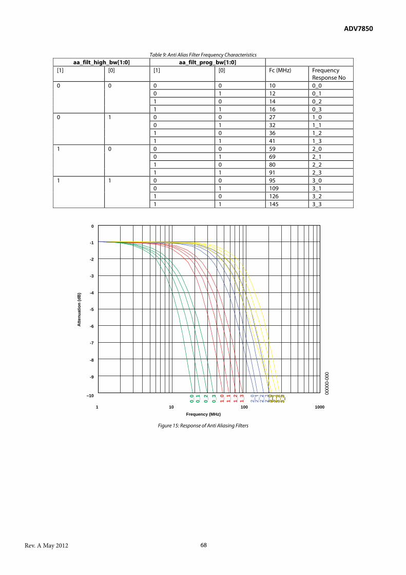
ADV7850
Rev. A May 2012 68
Table 9: Anti Alias Filter Frequency Characteristics aa_filt_high_bw[1:0] aa_filt_prog_bw[1:0]
[1] [0] [1] [0] Fc (MHz) Frequency Response No
0 0 0 0 10 0_0 0 1 12 0_1 1 0 14 0_2 1 1 16 0_3
0 1 0 0 27 1_0 0 1 32 1_1 1 0 36 1_2 1 1 41 1_3
1 0 0 0 59 2_0 0 1 69 2_1 1 0 80 2_2 1 1 91 2_3
1 1 0 0 95 3_0 0 1 109 3_1 1 0 126 3_2 1 1 145 3_3
Figure 15: Response of Anti Aliasing Filters
0
-9
–10
1 10 100 1000
0000
0-00
0
Atte
nuat
ion
(dB
)
Frequency (MHz)
-8
-7
-6
-5
-4
-3
-2
-1
0_0
0_1
0_2
0_3
1_0
1_1
1_2
1_3
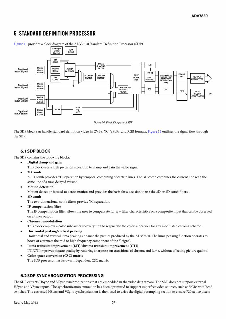
ADV7850
Rev. A May 2012 69
6 STANDARD DEFINITION PROCESSOR
Figure 16 provides a block diagram of the ADV7850 Standard Definition Processor (SDP).
Figure 16: Block Diagram of SDP The SDP block can handle standard definition video in CVBS, YC, YPbPr, and RGB formats. Figure 16 outlines the signal flow through the SDP.
6.1 SDP BLOCK The SDP contains the following blocks:
• Digital clamp and gain This block uses a high precision algorithm to clamp and gain the video signal.
• 3D comb A 3D comb provides YC separation by temporal combining of certain lines. The 3D comb combines the current line with the same line of a time delayed version.
• Motion detection Motion detection is used to detect motion and provides the basis for a decision to use the 3D or 2D comb filters.
• 2D comb The two-dimensional comb filters provide YC separation.
• IF compensation filter The IF compensation filter allows the user to compensate for saw filter characteristics on a composite input that can be observed on a tuner output.
• Chroma demodulation This block employs a color subcarrier recovery unit to regenerate the color subcarrier for any modulated chroma scheme.
• Horizontal peaking/vertical peaking Horizontal and vertical luma peaking enhance the picture produced by the ADV7850. The luma peaking function operates to boost or attenuate the mid to high frequency component of the Y signal.
• Luma transient improvement (LTI)/chroma transient improvement (CTI) LTI/CTI improves picture quality by restoring sharpness on transitions of chroma and luma, without affecting picture quality.
• Color space conversion (CSC) matrix The SDP processor has its own independent CSC matrix.
6.2 SDP SYNCHRONIZATION PROCESSING The SDP extracts HSync and VSync synchronizations that are embedded in the video data stream. The SDP does not support external HSync and VSync inputs. The synchronization extraction has been optimized to support imperfect video sources, such as VCRs with head switches. The extracted HSync and VSync synchronization is then used to drive the digital resampling section to ensure 720 active pixels
DigitisedInput Signal
DigitalClamp& Gain
MotionDetect
3DCOMB
2DCOMB
ALPHABLENDER
DigitisedInput Signal
DigitalClamp& Gain
DigitisedInput Signal
DigitalClamp& Gain
IF COMPFILTER
CHROMADEMOD
LUMASHAPINGFILTER
CHROMASHAPINGFILTER
FASTBLANK
MIX
DigitisedInput Signal
DigitalClamp& Gain
DELAYRGBTO
YUV
LTI
CTI
HORIZ+
VERTPEAKING
BRIGHTNESSCONTRAST
SATURATIONHUE
CSC
FRAMETBC
FIFO
OUTPUTFORMATTER
OUTPUTCLOCK
GENERATOR
AnalogueClampControl
SyncDetect

ADV7850
Rev. A May 2012 70
per line are output by the SDP. The ADV7850 uses a VSync and HSync PLL to provide an accurate and reliable lock for both perfect and imperfect video sources.
• VSync PLL: provides extra filtering of the detected VSyncs to give improved vertical lock. • HSync PLL: designed to filter incoming HSyncs corrupted by noise; providing much improved performance for video signals
with stable time base but poor signal to noise ratio (SNR). sdp_extend_vs_max_freq and sdp_extend_vs_min_freq can be used to additionally extend VSync lock ranges. sdp_extend_vs_max_freq, Addr 90 (SDP), Address 0x7B[2] This control is used to extend the minimum frequency VSync lock range.
Function sdp_extend_vs_max_freq
Description
1 Extended minimum frequency VSync lock range 0 Normal minimum frequency VSync lock range
sdp_extend_vs_min_freq, Addr 90 (SDP), Address 0x7B[1] This control is used to extend the maximum frequency VSync lock range.
Function sdp_extend_vs_min_freq
Description
1 Extended maximum frequency VSync lock range 0 Normal maximum frequency VSync lock range
6.3 SDP GENERAL SETUP
6.3.1 Autodetection of SDP Modes Automatic standard detection or specific standard forcing on the ADV7850 is achieved by specifying the standards to be automatically detected. The autodetection registers allows the user to force the digital core into a specific video standard. Setting the relevant bit to 0 inhibits the standard from being detected automatically. For example, to force the standard to PAL only the PAL autodetection bit should be set. To allow the decoder to detect automatically between PAL, NTSC, and SECAM, the appropriate bits should be set. The results of the SDP autodetection can be read back via the status registers. sdp_ad_secam_en, Addr 90 (SDP), Address 0x00[6] This control is used to enable autodetection of the SECAM standard. Setting this bit to 1 enables the corresponding standard to be detected. In order to force the part into a particular standard, only the corresponding enable bit for that standard should be enabled. To allow full autodetection, all standards should be enabled via the respective bit.
Function sdp_ad_secam_en Description 1 Enable SECAM to be detected 0 Do not enable SECAM to be detected
sdp_ad_n443_en, Addr 90 (SDP), Address 0x00[5] This control is used to enable autodetection of the NTSC-443 standard. Setting this bit to 1 enables the corresponding standard to be detected. In order to force the part into a particular standard, only the corresponding enable bit for that standard should be enabled. To allow full autodetection, all standards should be enabled via the respective bit.

ADV7850
Rev. A May 2012 71
Function sdp_ad_n443_en Description 1 Enable NTSC-443 to be detected 0 Do not enable NTSC-443 to be detected
sdp_ad_pal60_en, Addr 90 (SDP), Address 0x00[4] This control is used to enable autodetection of the PAL-60 standard. Setting this bit to 1 enables the corresponding standard to be detected. In order to force the part into a particular standard, only the corresponding enable bit for that standard should be enabled. To allow full autodetection, all standards should be enabled via the respective bit.
Function sdp_ad_pal60_en Description 1 Enable PAL-60 to be detected 0 Do not enable PAL-60 to be detected
sdp_ad_palcn_en, Addr 90 (SDP), Address 0x00[3] This control is used to enable autodetection of the PAL-CombN standard. Setting this bit to 1 enables the corresponding standard to be detected. In order to force the part into a particular standard, only the corresponding enable bit for that standard should be enabled. To allow full autodetection, all standards should be enabled via the respective bit.
Function sdp_ad_palcn_en Description 1 Enable PAL-CombN to be detected 0 Do not enable PAL-CombN to be detected
sdp_ad_palm_en, Addr 90 (SDP), Address 0x00[2] This control is used to enable autodetection of the PAL-M standard. Setting this bit to 1 enables the corresponding standard to be detected. In order to force the part into a particular standard, only the corresponding enable bit for that standard should be enabled. To allow full autodetection, all standards should be enabled via the respective bit.
Function sdp_ad_palm_en Description 1 Enable PAL-M to be detected 0 Do not enable PAL-M to be detected
sdp_ad_ntsc_en, Addr 90 (SDP), Address 0x00[1] This control is used to enable autodetection of the NTSC-M standard. Setting this bit to 1 enables the corresponding standard to be detected. In order to force the part into a particular standard, only the corresponding enable bit for that standard should be enabled. To allow full autodetection, all standards should be enabled via the respective bit.
Function sdp_ad_ntsc_en Description 1 Enable NTSC-M to be detected 0 Do not enable NTSC-M to be detected
sdp_ad_pal_en, Addr 90 (SDP), Address 0x00[0] This control is used to enable autodetection of the PAL-BGHID standard. Setting this bit to 1 enables the corresponding standard to be detected. In order to force the part into a particular standard, only the corresponding enable bit for that standard should be enabled. To allow full autodetection, all standards should be enabled via the respective bit.
ADV7850
Rev. A May 2012 72
Function sdp_ad_pal_en Description 1 Enable PAL-BGHID to be detected 0 Do not enable PAL-BGHID to be detected
6.3.2 Pedestal Configuration in SDP Modes The following controls dictate which standards the SDP core expects to have a pedestal. Standards that are expected to have a pedestal are clamped to the back porch level. sdp_pal_ped_en, Addr 90 (SDP), Address 0x01[0] This control is used to force the part to assume that the corresponding standard has a pedestal. Standards with a pedestal are clamped to the pedestal level; standards without a pedestal are clamped to the back porch level.
Function sdp_pal_ped_en Description 1 Assume PAL-BGHID inputs have a pedestal 0 Assume PAL-BGHID inputs do not have a pedestal
sdp_secam_ped_en, Addr 90 (SDP), Address 0x01[6] This control is used to force the part to assume that the corresponding standard has a pedestal. Standards with a pedestal are clamped to the pedestal level; standards without a pedestal are clamped to the back porch level.
Function sdp_secam_ped_en Description 1 Assume SECAM inputs have a pedestal 0 Assume SECAM inputs do not have a pedestal
sdp_n443_ped_en, Addr 90 (SDP), Address 0x01[5] This control is used to force the part to assume that the corresponding standard has a pedestal. Standards with a pedestal are clamped to the pedestal level; standards without a pedestal are clamped to the back porch level.
Function sdp_n443_ped_en Description 1 Assume NTSC-443 inputs have a pedestal 0 Assume NTSC-443 inputs do not have a pedestal
sdp_pal60_ped_en, Addr 90 (SDP), Address 0x01[4] This control is used to force the part to assume that the corresponding standard has a pedestal. Standards with a pedestal are clamped to the pedestal level; standards without a pedestal are clamped to the back porch level.
Function sdp_pal60_ped_en Description 1 Assume PAL-60 inputs have a pedestal 0 Assume PAL-60 inputs do not have a pedestal
sdp_palcn_ped_en, Addr 90 (SDP), Address 0x01[3] This control is used to force the part to assume that the corresponding standard has a pedestal. Standards with a pedestal are clamped to the pedestal level; standards without a pedestal are clamped to the back porch level.

ADV7850
Rev. A May 2012 73
Function sdp_palcn_ped_en Description 1 Assume PAL-CombN inputs have a pedestal 0 Assume PAL-CombN inputs do not have a pedestal
sdp_palm_ped_en, Addr 90 (SDP), Address 0x01[2] This control is used to force the part to assume that the corresponding standard has a pedestal. Standards with a pedestal are clamped to the pedestal level; standards without a pedestal are clamped to the back porch level.
Function sdp_palm_ped_en Description 1 Assume PAL-M inputs have a pedestal 0 Assume PAL-M inputs do not have a pedestal
sdp_ntsc_ped_en, Addr 90 (SDP), Address 0x01[1] This control is used to force the part to assume that the corresponding standard has a pedestal. Standards with a pedestal are clamped to the pedestal level; standards without a pedestal are clamped to the back porch level.
Function sdp_ntsc_ped_en Description 1 Assume NTSC-M inputs have a pedestal 0 Assume NTSC-M inputs do not have a pedestal
6.4 SDP STATUS REGISTERS The SDP contains registers that provide summary information about the video decoder. This information allows the user to read back information such as decoder lock status, input format and type, and autodetection result.
6.4.1 SDP Autodetection Result sdp_std[3:0], Addr 90 (SDP), Address 0x52[3:0] (Read Only) This readback displays the current active standard in autodetection mode.
Function sdp_std[3:0] Description 0x00 NTSC-M/J 0x02 NTSC-443 0x03 60HzSECAM 0x04 PAL-M 0x06 PAL-60 0x0C PAL-CombN 0x0E PAL-BGHID 0x0F SECAM
Refer to Section 6.3.1 for more information on the use of the autodetection block.
6.4.2 SDP Video Detection sdp_video_detected, Addr 90 (SDP), Address 0x5A[0] (Read Only) This readback indicates the detection of a valid video input.

ADV7850
Rev. A May 2012 74
Function sdp_video_detected Description 1 Indicates valid SD/PR video input detected 0 Input invalid or no input connected
sdp_c_chan_active, Addr 90 (SDP), Address 0x54[5] (Read Only) This readback displays the result of the CVBS/YC detection feature.
Function sdp_c_chan_active Description 1 Y/C input detected 0 CVBS input detected
sdp_pr_detected_in_sd, Addr 90 (SDP), Address 0x58[6] (Read Only) This readback indicates the detection of a progressive input to the SD core.
Function sdp_pr_detected_in_sd Description 1 SDP detects progressive input 0 Normal operation
6.4.3 Input Status The sdp_STATUS_INPUT_TYPE_1 register consists of the following fields. sdp_hswitch_present, Addr 90 (SDP), Address 0x56[7] (Read Only) This readback displays the result of head switch detection using algorithm 1.
Function sdp_hswitch_present Description 1 Head switch detected by algorithm 1 0 Head switch not detected by algorithm 1
sdp_blk_nstd, Addr 90 (SDP), Address 0x56[6] (Read Only) This readback displays the length of a 192 line block of pixels in clock cycles if within the set threshold.
Function sdp_blk_nstd Description 1 Length of 192 line block of pixels in clock cycles not within +- sdp_frm_nstd_thr of nominal
value 0 Length of 192 line block of pixels in clock cycles within +- sdp_frm_nstd_thr of nominal value
sdp_fld_nstd, Addr 90 (SDP), Address 0x56[5] (Read Only) This readback indicates if the field length in clock cycles is within the threshold set by sdp_frm_nstd_thr of a nominal value.
Function sdp_fld_nstd Description 1 Field length in clock cycles not within +- sdp_frm_nstd_thr of nominal value 0 Field length in clock cycles within +- sdp_frm_nstd_thr of nominal value
ADV7850
Rev. A May 2012 75
sdp_frm_nstd, Addr 90 (SDP), Address 0x56[4] (Read Only) This readback indicates if the frame length in clock cycles is within the threshold set by sdp_frm_nstd_thr.
Function sdp_frm_nstd Description 1 Frame length in clock cycles not within +- sdp_frm_nstd_thr of nominal value 0 Frame length in clock cycles within +- sdp_frm_nstd_thr of nominal value
sdp_lc_nstd, Addr 90 (SDP), Address 0x56[3] (Read Only) This readback indicates if the field length varies by more than one line from field to field.
Function sdp_lc_nstd Description 1 Field length in terms of number of lines varies by more than one line from field to field 0 Field length in terms of number of lines does not vary by more than one line from field to field
sdp_allow_med_pll, Addr 90 (SDP), Address 0x56[2] (Read Only) This readback indicates if the input could be from a VCR source. It is valid only if sdp_allow_slow_pll is set to 0. It is ignored if sdp_allow_slow_pll is set to 1.
Function sdp_allow_med_pll Description 1 Input may be a VCR; medium HSync PLL speed used 0 Input is a VCR; fast HSync PLL speed used
sdp_allow_slow_pll, Addr 90 (SDP), Address 0x56[1] (Read Only) This readback indicates if the input could be from a VCR source. It is to be used in conjunction with sdp_allow_med_pll.
Function sdp_allow_slow_pll Description 1 Input not a VCR; slow HSync PLL speed used 0 Input may be a VCR; refer to sdp_allow_med_pll
sdp_free_run, Addr 90 (SDP), Address 0x56[0] (Read Only) This readback indicates free run status. If set to 1, the part is free running due to no video detected on the input or forced free run mode.
Function sdp_free_run Description 1 Part free running 0 Part not free running
sdp_ckill_act, Addr 90 (SDP), Address 0x57[7] (Read Only) This readback displays the color kill status.
Function sdp_ckill_act Description 1 Color kill is active (and enabled) 0 Color kill is not active

ADV7850
Rev. A May 2012 76
sdp_vs_std_mode, Addr 90 (SDP), Address 0x57[6] (Read Only) This readback indicates the detection of regular frame lengths on the input.
Function sdp_vs_std_mode Description 1 Regular frame lengths detected on input 0 Regular frame lengths not detected on input
sdp_allow_3d_comb, Addr 90 (SDP), Address 0x57[4] (Read Only) This readback indicates the suitability of the input for 3D combing.
Function sdp_allow_3d_comb Description 1 Standard input detected, 3d comb allowed 0 Nonstandard input detected, 3d comb not allowed, 2d comb used
sdp_interlaced, Addr 90 (SDP), Address 0x57[3] (Read Only) This readback indicates the detection of an interlaced format on the input.
Function sdp_interlaced Description 1 Alternating field sequence detected on input 0 Alternating field sequence not detected on input
sdp_trick_mode, Addr 90 (SDP), Address 0x57[2] (Read Only) This readback indicates the detection of a VCR trick mode operation on the input.
Function sdp_trick_mode Description 1 VCR trick mode detected, line TBC allowed if enabled 0 VCR trick mode not detected, line TBC not allowed
sdp_burst_locked_rb, Addr 90 (SDP), Address 0x59[7] (Read Only) This readback displays the status of the burst locking loop.
Function sdp_burst_locked_rb Description 1 Burst locking loop locked 0 Burst locking loop not locked
sdp_ad_50_60_hz, Addr 90 (SDP), Address 0x59[3] (Read Only) This readback displays the result of the field rate detection on the input.
Function sdp_ad_50_60_hz Description 1 Field rate of 50 Hz detected on input 0 Field rate of 60 Hz detected on input

ADV7850
Rev. A May 2012 77
sdp_pal_sw_locked, Addr 90 (SDP), Address 0x59[2] (Read Only) This readback indicates the detection of a PAL swinging burst sequence on the input.
Function sdp_pal_sw_locked Description 1 PAL swinging burst sequence detected 0 PAL swinging burst sequence not detected
sdp_fsc_freq_ok, Addr 90 (SDP), Address 0x59[1] (Read Only) This readback indicates the status of the subcarrier frequency detected on the input if it is close to that of the selected standard, 3.58 MHz or 4.43 MHz; or the subcarrier frequency is running in 4.43 MHz input mode and input is 3.58 MHz or vice versa.
Function sdp_fsc_freq_ok Description 1 Detected fact frequency close to that of selected standard 0 Detected fact frequency not close to that of selected standard
sdp_scm_locked, Addr 90 (SDP), Address 0x59[0] (Read Only) This readback indicates the detection of a SECAM input.
Function sdp_scm_locked Description 1 SECAM detected on input 0 SECAM not detected on input
6.4.4 Macrovision Status Macrovision status bits are split into two registers, status_macrovision_detection_1 and status_macrovision_detection_2, located in the SDP Map at address 0x50 and 0x51 respectively. status_macrovision_detection_1 Register sdp_mv_agc_detected, Addr 90 (SDP), Address 0x50[3] (Read Only) This readback displays the detection of Macrovision AGC pulses.
Function sdp_mv_agc_detected Description 1 Macrovision AGC pulses part of AGC process detected 0 Macrovision AGC pulses part of AGC process not detected
sdp_mv_ps_detected, Addr 90 (SDP), Address 0x50[2] (Read Only) This readback displays the detection of Macrovision AGC pseudo syncs.
Function sdp_mv_ps_detected Description 1 Macrovision pseudo sync part of AGC process detected 0 Macrovision pseudo sync part of AGC process not detected

ADV7850
Rev. A May 2012 78
sdp_mvcs_type3, Addr 90 (SDP), Address 0x50[1] (Read Only) This readback displays the detection of a Macrovision type 3 color stripe process.
Function sdp_mvcs_type3 Description 1 Macrovision type 3 color stripe process detected, only valid if sdp_mvcs_detect = 1 0 Macrovision type 3 color stripe process not detected
sdp_mvcs_detect, Addr 90 (SDP), Address 0x50[0] (Read Only) This readback displays the detection of the color stripe process.
Function sdp_mvcs_detect Description 1 Macrovision color stripe process detected 0 Macrovision color stripe process not detected
status_macrovision_detection_2 Register sdp_bp_total_pulse_beg[3:0], Addr 90 (SDP), Address 0x51[7:4] (Read Only) This readback displays the total Macrovision back porch pulses detected at the beginning of the field. sdp_bp_total_pulses_end[3:0], Addr 90 (SDP), Address 0x51[3:0] (Read Only) This readback displays the total Macrovision back porch pulses detected at the end of the field.
6.4.5 Synctip Noise Measurement, Noisy and Very Noisy Signal Detection sdp_synctip_noise[11:0] is a readback value of the average of the noise in the HSync tip. sdp_synctip_noise[11:0] is spread over two complete I2C registers, allowing the user to read eight MSBs or eight LSBs of synctip noise in one I2C read transfer. 1 bit of sdp_synctip _noise[11:0] = 1 ADC code 1 bit of sdp_synctip _noise[11:0] = 398.883 uV sdp_synctip_noise[11:0], Addr 90 (SDP), Address 0x53[7:4]; Address 0x4F[7:0] (Read Only) This readback indicates the noise level on the synctip of the video signal.
Function sdp_synctip_noise[11:0]
Description
0x53[7:4] sdp_synctip_noise[11:8] 0x4F[7:0] sdp_synctip_noise[7:0]
Note that register 0x53[3:0] contains sdp_synctip_noise[7:4]. The polling of a single register in 0x53[7:0] reads back the MSBs of sdp_synctip_noise[11:4]. The polling of a single register in 0x4F[7:0] reads back the LSBs of sdp_synctip_noise[7:0]. The user has to read back both registers (0x53 and 0x4F) to obtain the full noise measurement from sdp_synctip_noise[11:0]. The sdp_noisy_ip and sdp_very_noisy_ip bits can be used to check the quality of the video signal. These bits are located in the SDP Map in register 0x54. By doing a single readback of register 0x54, the quality of the video signal can be determined quickly. sdp_noisy_thr[7:0] and sdp_very_noisy_thr[7:0] are used to set the threshold for the input to detect a signal as noisy or very noisy. The following controls are used in conjunction with the bits used for 3D comb activation (refer to Section 6.7.1):

ADV7850
Rev. A May 2012 79
• sdp_noisy_hsw2_dis_3d • sdp_noisy_hsw1_dis_3d • sdp_noisy_lc_dis_3d • sdp_noisy_blk_dis_3d • sdp_noisy_fld_dis_3d • sdp_noisy_frm_dis_3d • sdp_noisy_dis_3d • sdp_vnoisy_hsw2_dis_3d • sdp_vnoisy_hsw1_dis_3d • sdp_vnoisy_lc_dis_3d • sdp_vnoisy_blk_dis_3d • sdp_vnoisy_fld_dis_3d • sdp_vnoisy_frm_dis_3d • sdp_vnoisy_dis_3d
sdp_noisy_ip, Addr 90 (SDP), Address 0x54[7] (Read Only) This readback displays the detection of a noisy input signal.
Function sdp_noisy_ip Description 1 Noisy input detected 0 Noisy input not detected
sdp_very_noisy_ip, Addr 90 (SDP), Address 0x54[6] (Read Only) This readback displays the detection of a very noisy input signal.
Function sdp_very_noisy_ip Description 1 Very noisy input detected 0 Very noisy input not detected
sdp_noisy_thr[7:0], Addr 90 (SDP), Address 0xA1[7:0] This control is used to set the threshold for input to be detected as noisy. A higher value reduces the possibility of detecting an input as noisy. sdp_very_noisy_thr[7:0], Addr 90 (SDP), Address 0xA2[7:0] This control is used to set the threshold for input to be detected as very noisy. A higher valued reduces the possibility of detecting the input to be very noisy.
6.4.6 Additional SDP Status Registers An indication of signal strength can be obtained by reading back the burst power of the signal. The ADV7850 allows for two burst power measurements burst_power_act[11:0], Addr 94 (SDP_IO), Address 0x44[3:0]; Address 0x45[7:0] (Read Only) This readback displays the active path burst power measurement.

ADV7850
Rev. A May 2012 80
Function burst_power_act[11:0] Description 0xXXX Burst Power Readback value
burst_power_ad[11:0], Addr 94 (SDP_IO), Address 0x46[3:0]; Address 0x47[7:0] (Read Only) This readback displays the autodetect path burst power measurement.
Function burst_power_ad[11:0] Description 0xXXX Burst Power Readback value
hs_period_err_raw[11:0], Addr 94 (SDP_IO), Address 0x4A[3:0]; Address 0x4B[7:0] (Read Only) This readback displays the raw HSync period error.
Function hs_period_err_raw[11:0]
Description
0xXXX Raw HSync readback value hs_period_err_filt[11:0], Addr 94 (SDP_IO), Address 0x4C[3:0]; Address 0x4D[7:0] (Read Only) This readback displays the filtered HSync period error.
Function hs_period_err_filt[11:0] Description 0xXXX Filtered HSync readback value
hs_period_valid, Addr 94 (SDP_IO), Address 0x4E[0] (Read Only) This readback displays the HSync period measurement valid flag.
Function hs_period_valid Description 0 hs_period_err_filt readback invalid 1 hs_period_err_filt readback valid
upd_sdp_rb, Addr 94 (SDP_IO), Address 0x4F[0] (Self-Clearing) This control is used to update the c_gain_act, c_gain_ad, burst_power_act, burst_power_ad, hs_period_err_raw and hs_period_err_filt readback registers.
Function upd_sdp_rb Description 0 << Freeze SDP multiregister readbacks 1 Update SDP multiregister readbacks
6.5 SDP COLOR CONTROLS The following registers provide user control over the picture appearance. They are independent of any other controls. For instance, the brightness control is independent of the picture clamping, although both controls affect the DC level of the signal. The ADV7850 provides 10-bit control of contrast, brightness, saturation, and hue.
ADV7850
Rev. A May 2012 81
6.5.1 Contrast sdp_contrast[9:0], Addr 90 (SDP), Address 0x13[7:0]; Address 0x17[1:0] This control is used to set the contrast level (luma gain). This control has a range of 0 to 2. It is an unsigned number and has a range from 0x000 (lowest contrast, all black) to 0x3FF (highest contrast).
Function sdp_contrast[9:0] Description 0x000 Lowest contrast 0x080 Default contrast 0x3FF Highest contrast
6.5.2 Brightness sdp_brightness[9:0], Addr 90 (SDP), Address 0x14[7:0]; Address 0x17[3:2] This control is used to set the brightness level (luma offset). It is a twos compliment number and has a range of 0x200 (darkest) to 0x1FF (brightest).
Function sdp_brightness[9:0] Description 0x200 Darkest 0x000 Default brightness 0x1FF Brightest
6.5.3 Saturation sdp_saturation[9:0], Addr 90 (SDP), Address 0x15[7:0]; Address 0x17[5:4] This control is used to set the saturation level (chroma gain). It has a valid range of 0 to 1.75. It is an unsigned number and has a range of 0x000 (lowest saturation, no color) to 0x3FF (highest saturation).
Function sdp_saturation[9:0] Description 0x000 Lowest saturation (no color) 0x3FF Highest saturation
6.5.4 Hue sdp_hue[9:0], Addr 90 (SDP), Address 0x16[7:0]; Address 0x17[7:6] This control is used to set the hue (chroma phase rotation). It is a twos compliment number and has a range of 0x200 (-180 degrees) to 0x1FF (+180 degrees).
Function sdp_hue[9:0] Description 0x1FF +180° 0x000 0° 0x200 -180°
6.6 SDP GAIN OPERATION The SDP gain control within the ADV7850 is done on a purely digital basis. SDP gain correction takes place after digitization in the form of a digital multiplier.

ADV7850
Rev. A May 2012 82
Figure 17: SDP Gain Control Overview
As shown in Figure 17, the ADV7850 can decode a video signal as long as it fits into the ADC window. There are two components; the amplitude of the input signal, and the DC level on which it resides. The DC level is set by the clamping circuitry. If the amplitude of the analog video signal is too high, clipping can occur and visual artifacts appear. The analog input range of the ADC and the clamp level determine the maximum supported amplitude of the video signal. The minimum supported amplitude of the input video is determined by the core ability of the SDP to retrieve horizontal and vertical timing and to lock to the color burst, if present. There are two gain control units, one for luma data and the other for chroma data. Both operate independently of each other. The luma gain controls operate in three basic modes:
• Manual gain. The gain can be controlled manually irrespective of peak white.
• Automatic gain control (AGC) with peak white adjustment. The peak white feature overrides and reduces the gain of the luma AGC if the input signal exceeds a specific threshold.
• Automatic gain control without peak white adjustment. The applied luma gain values can be read back using sdp_y_gain_man_rb[12:0]. The chroma gain controls operate in a similar way. Peak black overrides and increases the gain of the luma AGC if the input signal becomes lower than a set threshold. Peak black is not user controllable.
6.6.1 SDP Luma Gain sdp_y_agc_en, Addr 90 (SDP), Address 0x03[7] This control is used to select between automatic and manual luma gain control.
Function sdp_y_agc_en Description 1 Enable automatic luma gain based on sync 0 Enable manual luma gain, set by sdp_y_gain_man
sdp_man_gain_vcr, Addr 90 (SDP), Address 0x03[5] This control is used to select the gain method used when a VCR input is detected.
X
Analog Voltage Range Supported by ADC (1.0V Range)
Clamp Level
Maximum Voltage
ADC
Minimum Voltage
Gain Control
(Gain Section only)

ADV7850
Rev. A May 2012 83
Function sdp_man_gain_vcr Description 1 Manual gain used for VCR inputs value is sdp_y_gain_man 0 Automatic gain used for VCR inputs (valid only if sdp_y_agc_en set to 1)
sdp_y_gain_man[12:0], Addr 90 (SDP), Address 0x03[4:0]; Address 0x04[7:0] This control is used to adjust the manual luma gain value. It is used if sdp_y_agc_en is set to 0. It also applies to the G channel in component modes. The control has a range of 0.5 to 4.
Function sdp_y_gain_man[12:0] Description 0x0558 Default
Luma_Gain = 1024
4095]0:12[___512 ≤< MANGAINYSDP = 0.5…4.0
Equation 1: SDP Luma Gain Formula
The luma gain range is from 0.5 to 4.0. Example: To program the ADV7850 into manual fixed gain mode with a desired gain of 0.95:
• Use Equation 1 to convert the gain: 0.95 * 1024 = 972.8
• Truncate to integer value: 972.8 972
• Convert to hexadecimal: 972 0x3CC
• Split into two registers and program: sdp_y_gain_man[12:8] = 0x3
sdp_y_gain_man[7:0] = 0xCC • Enable manual fixed gain mode:
Set sdp_y_agc_en to 0 sdp_y_gain_man_rb[12:0], Addr 90 (SDP), Address 0x54[4:0]; Address 0x55[7:0] (Read Only) This readback provides the current luma gain.
Function sdp_y_gain_man_rb[12:0]
Description
0x54[4:0] sdp_y_gain_man_rb[12:8] 0x55[7:0] sdp_y_gain_man_rb[7:0]
sdp_limit_y_gain, Addr 90 (SDP), Address 0x89[7] This control is used to limit the luma gain.
Function sdp_limit_y_gain Description 1 Limit luma gain to range of 50% to 200% 0 Normal operation

ADV7850
Rev. A May 2012 84
sdp_dgain_speed[4:0], Addr 90 (SDP), Address 0x0A[4:0] This control is used to adjust the speed of luma digital gain operation. Only values of 1 to 6 are within a valid range.
Function sdp_dgain_speed[4:0] Description 0x00 Freeze digital gain 0x05 Default Valid range 0x01 to 0x06 All other values Reserved
6.6.2 Chroma Gain sdp_c_agc_en, Addr 90 (SDP), Address 0x05[7] This control is used to select between automatic and manual chroma gain (C/U/V/R/B channels also used for G in the case of SCART).
Function sdp_c_agc_en Description 1 Enable automatic chroma gain based on burst power 0 Enable manual chroma gain, gain value set by sdp_c_gain_act_man
sdp_c_gain_act_man[12:0], Addr 90 (SDP), Address 0x05[4:0]; Address 0x06[7:0] This control is used to adjust the manual chroma gain value. It used if sdp_c_agc_en is set to 0. It also applies to the U, V, R, and B channels in component modes. The control has a range of 0.5 to 8.
Function sdp_c_gain_act_man[12:0]
Description
0x05[4:0] sdp_c_gain_act_man[12:8] 0x06[7:0] sdp_c_gain_act_man[7:0]
Chroma_Gain = 1024
8191____512 << manactgaincsdp = 0.5…8.0
Equation 2: SDP Chroma Gain Formula
The chroma gain range is from 0.5 to 8.0. Example: To program the ADV7850 into manual fixed chroma gain with a desired gain of 0.70 (signal):
• Use Equation 2 to convert the gain: 0.70 * 1024 = 716.8
• Truncate to integer value: 716.8 716
• Convert to hexadecimal: 716 0x2CC
• Split into two registers and program: sdp_c_gain_act _man[12:8] = 0x2
sdp_c_gain_act _man[7:0] = 0xCC • Enable manual fixed gain mode:
Set sdp_c_agc_en to 0 sdp_limit_c_gain, Addr 90 (SDP), Address 0x89[6] This control is used to limit the chroma gain.
ADV7850
Rev. A May 2012 85
Function sdp_limit_c_gain Description 1 Limit chroma gain to range of 50% to 200% 0 Normal operation
sdp_limit_uv_gain, Addr 90 (SDP), Address 0x89[5] This control is used to limit U/V gain.
Function sdp_limit_uv_gain Description 1 Limit U/V gain to range of 50% to 200% 0 Normal operation
sdp_limit_g_gain, Addr 90 (SDP), Address 0x89[4] This control is used to limit the SD SCART FB RGB gain.
Function sdp_limit_g_gain Description 1 Limit SD (FB) RGB gain to range of 50% to 200% 0 Normal operation
sdp_c_dgain_speed[4:0], Addr 90 (SDP), Address 0x0B[4:0] This control is used to adjust the speed of chroma digital gain operation. Only values of 1 to 6 are within a valid range. This register has an effect only if sdp_c_agc_en is set to 1.
Function sdp_c_dgain_speed[4:0]
Description
00000 Freeze clamp gain Valid range 1 to 6 All other values Reserved
sdp_c_dgain_speed[4:0] allows the user to influence the tracking speed of the chroma automatic gain control. Note that this control has an effect only if sdp_c_agc_en is set to 1 (automatic gain). A setting of 0 freezes the chroma digital gain. The larger the register value, the faster the loop operates. Values above 0x06 are reserved.
6.6.3 Peak White Feature sdp_pw_en, Addr 90 (SDP), Address 0x03[6] This control is used to enable the peak white luma gain feature.
Function sdp_pw_en Description 1 Enable peak white luma gain control 0 Disable peak white luma gain control
sdp_pw_rec_rate[11:0], Addr 90 (SDP), Address 0x0F[3:0]; Address 0x10[7:0] This control is used to adjust the peak white gain recovery speed, that is, the speed at which the luma gain is increased following a gain reduction to a peak white violation. A larger value corresponds to a faster speed.

ADV7850
Rev. A May 2012 86
Function sdp_pw_rec_rate[11:0] Description 0x0F[3:0] sdp_pw_rec_rate[12:8] 0x10[7:0] sdp_pw_rec_rate[7:0]
6.6.4 Peak Chroma sdp_pc_en, Addr 90 (SDP), Address 0x05[6] This control is used to enable the peak-color chroma gain feature. Peak-color chroma overrides and reduces the gain of the chroma AGC if the chroma signal path becomes larger than a set threshold. Peak chroma can only act to reduce the AGC gain. When there are no more violations of the peak white threshold, the peak chrome algorithm allows the chroma AGC to restore the gain (based on the synchronization depth). The recovery rate of the AGC gain is set by the peak chroma recovery register.
Function sdp_pc_en Description 1 Enable peak color chroma gain 0 Disable peak color override of chroma gain
sdp_pc_rec_rate[11:0], Addr 90 (SDP), Address 0x0F[7:4]; Address 0x11[7:0] This control is used to adjust the peak chroma gain recovery speed, that is, the speed at which the chroma gain is increased following a gain reduction due to peak color violation. A larger value corresponds to a faster speed.
Function sdp_pc_rec_rate[11:0] Description 0x0F[7:4] sdp_pc_rec_rate[12:8] 0x11[7:0] sdp_pc_rec_rate[7:0]
6.6.5 Color Kill Color kill mode is the feature of the ADI decoder that allows the removal of chroma when the color burst level of the input is poor. This feature is especially useful when inputting weak-signal tuner signals. sdp_ckill_en, Addr 90 (SDP), Address 0x07[7] This control is used to enable the color kill feature.
Function sdp_ckill_en Description 1 Enable color kill feature 0 Disable color kill feature
sdp_ck_low_thr[6:0], Addr 90 (SDP), Address 0x07[6:0] This control is used to set the color kill low threshold. If the burst power is below this threshold, it enters color kill mode.
Function sdp_ck_low_thr[6:0] Description 00001011 Color kill low threshold
sdp_ck_high_thr[7:0], Addr 90 (SDP), Address 0x08[7:0] This control is used to set the color kill high threshold. If the burst power is above this threshold, it enters color kill mode.

ADV7850
Rev. A May 2012 87
Function sdp_ck_high_thr[7:0] Description 00011010 Color kill high threshold
6.7 3D COMB The ADV7850 has the ability to separate the luminance (Y) and chrominance (C) components using 1D (horizontal), 2D (horizontal and vertical), or 3D (temporal) processing.
Figure 18: 3D Comb and Motion Detection Operation When the picture content is static, the 3D comb filter in the ADV7850 combines video frames to give perfect Y/C separation results. Artifacts of 1D and 2D methods such as dot crawl, cross color, and hanging dots are eliminated. The sharpness and stillness of the decoded picture are improved using the 3D comb. Once the picture content begins to move, 3D Y/C separation is no longer possible and 2D or 1D combing must be used instead. The ADV7850 features advanced motion detection, enabling motion adaptive combing between 3D and 2D or 1D Y/C separation methods. This maximizes the benefit from 3D processing while minimizing temporal artifacts on moving picture regions. Note: 3D combing requires video frame storage in external memory. Where external memory is not connected, sdp_3d_comb_en must be disabled.
6.7.1 3D Comb Activation sdp_3d_comb_en, Addr 90 (SDP), Address 0x12[0] This control is used to disable the 3D comb filter. When the 3D comb is enabled, automatic 2D/3D comb switching is applied based on the detected video type. When the 3D comb is disabled, 2D combing only is applied.
Off-chipFrame
Memory
On-chipLine
Memories3D Comb
Filter
2D CombFilter
YMixer
CMixer
Per -pixel Y & Cmot ion est imates
Current(input)frame 2D Y
3D Y
3D C
2D C
Y out
C out
Delayedframe s
CVBS
MotionDetection
Video lines from first delayed frame
Video lines from current frame

ADV7850
Rev. A May 2012 88
Function sdp_3d_comb_en Description 1 Enable 3D comb filter 0 Disable 3D comb filter, enable 2D comb mode only
sdp_allow_3d_comb indicates if the ADV7850 has detected a non standard input for which 3D processing is not possible. For high quality PAL and NTSC input signals with nominal timebase, 3D processing is possible. For unstable, noisy, or otherwise non standard video signals, 3D processing is impossible. The user can disable 3D processing manually via sdp_3d_comb_en. The ADV7850 applies a deglitching filter to the result of this decision, with the programmable time constant controlled by sdp_allow_3d_filt_sel[2:0]. sdp_allow_3d_filt_sel[2:0], Addr 90 (SDP), Address 0x9A[2:0] This control is used to set the time constant applied to the deglitching filter for the 3D comb decision.
Function sdp_allow_3d_filt_sel[2:0]
Description
000 No filtering 001 0.25 sec 010 0.55 sec 011 0.81 sec 100 1.10 sec 101 1.36 sec 110 1.63 sec 111 2.00 sec
The ADV7850 monitors the input signal for noise and characteristics that are undesirable for 3D processing (information about noisy or very noisy input signal is accessible via sdp_very_noisy_ip and sdp_noisy_ip). The ADV7850 characterizes the signal as a clean, noisy, or very noisy input signal, and assesses whether or not the input signal has the following characteristics:
• Incorrect number of lines • Non standard block length • Non standard frame length • Non standard field length • VCR head switches (unstable time base) • No color burst (color kill is active)
For each input signal characterization (clean, noisy, or very noisy), it is possible to select whether or not the 3D comb is disabled on detection of the above characteristics. Note that 3D processing, if enabled with non standard inputs, can cause undesirable artifacts. The following controls allow the user to select the non standard characteristics that contribute to the sdp_allow_3d_comb decision. sdp_ckill_dis_3d, Addr 90 (SDP), Address 0xA3[7] This control is used to enable 3D combing if color kill mode is active.
Function sdp_ckill_dis_3d Description 1 Disable 3D comb if color kill active 0 Allow 3D comb even if color kill active

ADV7850
Rev. A May 2012 89
sdp_ckill_dis_2d, Addr 90 (SDP), Address 0xA4[7] This control is used to enable 2D combing even if color kill mode is active. This would effectively be passthrough mode.
Function sdp_ckill_dis_2d Description 1 Disable 2D comb if color kill active 0 Use 2D comb even if color kill active
sdp_noisy_hsw2_dis_3d, Addr 90 (SDP), Address 0xA4[6] This control is used to enable 3D combing if a noisy input is detected and headswitch is detected on the input by algorithm 2.
Function sdp_noisy_hsw2_dis_3d
Description
1 Disable 3D comb if noisy input detected and head switch detection algorithm 2 detects head switches
0 Allow 3D comb if noisy input detected even if head switch detection algorithm 2 detects head switches
sdp_noisy_hsw1_dis_3d, Addr 90 (SDP), Address 0xA4[5] This control is used to enable 3D combing if a noisy input is detected and a headswitch is detected on the input by algorithm 1.
Function sdp_noisy_hsw1_dis_3d
Description
1 Disable 3D comb if noisy input detected and head switch detection algorithm 1 detects head switches
0 Allow 3D comb if noisy input detected even if head switch detection algorithm 1 detects head switches
sdp_noisy_lc_dis_3d, Addr 90 (SDP), Address 0xA4[4] This control is used to enable 3D combing if a noisy input is detected and a nonstandard number of lines per frame is detected on the input.
Function sdp_noisy_lc_dis_3d Description 1 Disable 3D comb if noisy input detected and incorrect lines per frame detected 0 Allow 3D comb if noisy input detected even if incorrect number of lines per frame detected
sdp_noisy_blk_dis_3d, Addr 90 (SDP), Address 0xA4[3] This control is used to enable 3D combing if a noisy input is detected and a nonstandard block length is detected on the input.
Function sdp_noisy_blk_dis_3d Description 1 Disable 3D comb if noisy input detected and sdp_blk_nstd detected 0 Allow 3D comb if noisy input detected even if sdp_blk_nstd detected
sdp_noisy_fld_dis_3d, Addr 90 (SDP), Address 0xA4[2] This control is used to enable 3D combing if a noisy input is detected and a nonstandard field length is detected.

ADV7850
Rev. A May 2012 90
Function sdp_noisy_fld_dis_3d Description 1 Disable 3D comb if noisy input detected and sdp_fld_nstd detected 0 Allow 3D comb if noisy input detected even if sdp_fld_nstd detected
sdp_noisy_frm_dis_3d, Addr 90 (SDP), Address 0xA4[1] This control is used to enable 3D combing if a noisy input is detected and a nonstandard frame length is detected.
Function sdp_noisy_frm_dis_3d Description 1 Disable 3D comb if noisy input detected and sdm_frm_nstd detected 0 Allow 3D comb if noisy signal even if sdm_frm_nstd detected
sdp_noisy_dis_3d, Addr 90 (SDP), Address 0xA4[0] This control is used to enable 3D combing if a noisy input is detected.
Function sdp_noisy_dis_3d Description 1 Disable 3D comb if noisy input detected 0 Allow 3D comb if noisy input detected
sdp_p60_n443_dis_3d, Addr 90 (SDP), Address 0xA5[7] This control is used to enable 3D combing for PAL-60 and NTSC-443 even though it does not work perfectly due to a suboptimal mathematical relationship of subcarrier frequency versus horizontal frequency for those standards.
Function sdp_p60_n443_dis_3d Description 1 Disable 3D comb for PAL-60 and NTSC-443 inputs 0 Use 3D comb on PAL-60 and NTSC-443 inputs
sdp_vnoisy_hsw2_dis_3d, Addr 90 (SDP), Address 0xA5[6] This control is used to enable 3D combing if a very noisy input is detected and head switch is detected on the input by algorithm 2.
Function sdp_vnoisy_hsw2_dis_3d
Description
1 Disable 3D comb if very noisy input detected and head switch detection algorithm 2 detects head switches
0 Allow 3D comb if very noisy input detected even if head switch detection algorithm 2 detects head switches
sdp_vnoisy_hsw1_dis_3d, Addr 90 (SDP), Address 0xA5[5] This control is used to enable 3D combing if a very noisy input is detected and head switch is detected on the input by algorithm 1.

ADV7850
Rev. A May 2012 91
Function sdp_vnoisy_hsw1_dis_3d
Description
1 Disable 3D comb if very noisy input detected and head switch detection algorithm 1 detects head switches
0 Allow 3D comb if very noisy input detected even if head switch detection algorithm 1 detects head switches
sdp_vnoisy_lc_dis_3d, Addr 90 (SDP), Address 0xA5[4] This control is used to enable 3D combing if a very noisy input is detected and an incorrect frame length is detected on the input.
Function sdp_vnoisy_lc_dis_3d Description 1 Disable 3D comb if very noisy input detected and incorrect lines per frame detected 0 Allow 3D comb if very noisy input detected even if incorrect number of lines per frame
detected sdp_vnoisy_blk_dis_3d, Addr 90 (SDP), Address 0xA5[3] This control is used to enable 3D combing if a very noisy input is detected and a nonstandard block length is detected on the input.
Function sdp_vnoisy_blk_dis_3d Description 1 Disable 3D comb if very noisy input detected and sdp_blk_nstd detected 0 Allow 3D comb if very noisy input detected even if sdp_blk_nstd detected
sdp_vnoisy_fld_dis_3d, Addr 90 (SDP), Address 0xA5[2] This control is used to enable 3D combing if a very noisy input is detected and a nonstandard field length is detected on the input.
Function sdp_vnoisy_fld_dis_3d Description 1 Disable 3D comb if very noisy input detected and sdp_fld_nstd detected 0 Allow 3D comb if very noisy input detected even if sdp_fld_nstd detected
sdp_vnoisy_frm_dis_3d, Addr 90 (SDP), Address 0xA5[1] This control is used to enable 3D combing if a very noisy input is detected and a nonstandard frame length is detected on the input.
Function sdp_vnoisy_frm_dis_3d Description 1 Disable 3D comb if very noisy input and sdp_frm_nstd detected 0 Allow 3D comb if very noisy signal even if sdp_frm_nstd detected
sdp_vnoisy_dis_3d, Addr 90 (SDP), Address 0xA5[0] This control is used to enable 3D combing if a very noisy input is detected.
Function sdp_vnoisy_dis_3d Description 1 Disable 3d comb if very noisy input detected 0 Allow 3d comb if very noisy input detected

ADV7850
Rev. A May 2012 92
6.7.2 3D Comb Sensitivity sdp_3d_comb_luma_sns[3:0], Addr 90 (SDP), Address 0xAA[3:0] This control is used to set the 3D comb luma sensitivity. Larger values increase 3D comb motion detection sensitivity to luma motion and noise. This is an unsigned control.
Function sdp_3d_comb_luma_sns[3:0]
Description
1000 Smaller values increase 3D processing sdp_3d_comb_luma_core[3:0], Addr 90 (SDP), Address 0xAA[7:4] This control is used to set the 3D comb luma coring. Larger values decrease 3D comb motion detection sensitivity to luma motion and noise. This is an unsigned control.
Function sdp_3d_comb_luma_core[3:0]
Description
1000 Larger values increase 3D processing sdp_3d_comb_chroma_sns[3:0], Addr 90 (SDP), Address 0xA9[3:0] This control is used to set 3D comb chroma sensitivity. Larger values increase 3D comb motion detection sensitivity to chroma motion and noise. This is an unsigned control.
Function sdp_3d_comb_chroma_sns[3:0]
Description
1000 Smaller values increase 3D processing sdp_3d_comb_chroma_core[3:0], Addr 90 (SDP), Address 0xA9[7:4] This control is used to set 3D comb chroma coring. Larger values decrease 3D comb motion detection sensitivity to chroma motion and noise. This is an unsigned control.
Function sdp_3d_comb_chroma_core[3:0]
Description
1000 Larger values increase 3D processing sdp_3d_comb_noise_sns[6:0], Addr 90 (SDP), Address 0xA8[6:0] This control is used to set the 3D comb noise sensitivity. Larger values allow more temporal comb for noisy RF signals but may also introduce motion error. This is an unsigned control.
Function sdp_3d_comb_noise_sns[6:0]
Description
1000000 Smaller values increase 3D processing
6.8 Y SHAPING FILTER The Y shaping filter block is a programmable low pass filter with a wide variety of responses. It can be used to selectively reduce the bandwidth of the luma video signal. For some video sources that contain high frequency noise, reducing the bandwidth of the luma signal

ADV7850
Rev. A May 2012 93
improves visual picture quality. This feature can also be used to reduce the bandwidth of the luma video as required prior to scaling. For input signals in CVBS format, the luma shaping filters play an important role in removing the chroma component from a composite signal. YC separation must aim for the best possible crosstalk reduction while still retaining as much bandwidth as possible, especially on the luma component. The ADV7850 contains 33 different Y shaping filters available for selection using a 6-bit selection value. Four selection registers are provided so that different Y shaping filter can be selected for the VBI region, high quality inputs, low quality inputs, and SECAM inputs. The quality of the input signal is based on the HSync PLL speed, and some or all of the following metrics:
• Input is noisy (based on synchronization tip noise measurement and noisy threshold) • Head switch detected (indicating the input is from a VCR) • Input has incorrect number of lines per frame • Block length is non standard • Field length is non standard • Frame length is non standard • Input is very noisy (based on synchronization tip nose measurement and very noisy threshold)
Each of these metrics has an enable/disable bit to specify if it is included in the quality determination of the input signal. The amount of filtering on the standard/non standard decision for these metrics is user programmable from no filtering up to two seconds. There is also a single bit control to disable all of these metrics, and base the quality decision solely on the HSync PLL speed. A filter selection guide is used to choose the appropriate filter depending on the input signal format, type, quality, and user settings. In automatic mode, the system preserves the maximum possible bandwidth for good CVBS sources since they can be combed successfully, as well as for luma components of YUV and YC sources since they need not be combed. For poor quality signals, the system selects from a set of proprietary shaping filter responses that complement the comb filter operation in order to reduce visual artifacts. Table 10 lists the selectable filters types. A flow diagram showing the selection process is shown in Figure 19. Filter response plots are included from Figure 20 to Figure 25.
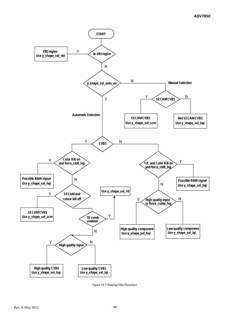
ADV7850
Rev. A May 2012 94
Figure 19: Y Shaping Filter Flowchart
In VBI region
y_shape_sel_auto_en
VBI regionUse y_shape_sel_vbi
START
SECAM CVBS
SECAM CVBSUse y_shape_sel_scm
Not SECAM CVBSUse y_shape_sel_hqi
Manual Selection
Y
Y
N
N
N
CVBS
Automatic Selection
NY
Color Kill onand force_ckill_hqi
Possible B&W signalUse y_shape_sel_hqi
SECAM CVBSUse y_shape_sel_scm
SECAM andcolour kill off
Y/C and Color Kill onand force_ckill_hqi
Possible B&W signalUse y_shape_sel_hqi
High quality inputor force_comp_hqi
1D combenabled
High quality componentUse y_shape_sel_hqi
Low quality componentUse y_shape_sel_lqi
High quality input
Use y_shape_sel_hqiHigh quality CVBS Low quality CVBS
Use y_shape_sel_lqi
Use y_shape_sel_1d
Y
Y
Y
Y
Y
Y
N
N
N
N
N
Y

ADV7850
Rev. A May 2012 95
Table 10: Y Shaping Filter Selection
No. Y Shape Response Filter Type Comment 0 General purpose low-pass luma shaping filter 1 FIR, linear Narrowest GPLPF 1 General purpose low-pass luma shaping filter 2 FIR, linear - 2 General purpose low-pass luma shaping filter 3 FIR, linear - 3 General purpose low-pass luma shaping filter 4 FIR, linear - 4 General purpose low-pass luma shaping filter 5 FIR, linear - 5 General purpose low-pass luma shaping filter 6 FIR, linear - 6 General purpose low-pass luma shaping filter 7 FIR, linear - 7 General purpose low-pass luma shaping filter 8 FIR, linear - 8 General purpose low-pass luma shaping filter 9 FIR, linear - 9 General purpose low-pass luma shaping filter 10 FIR, linear - 10 General purpose low-pass luma shaping filter 11 FIR, linear - 11 General purpose low-pass luma shaping filter 12 FIR, linear 12 General purpose low-pass luma shaping filter 13 FIR, linear - 13 General purpose low-pass luma shaping filter 14 FIR, linear Widest Fsc GPLPF 14 PAL/NTSC CVBS combined low-pass and Fsc notch shaping
filter 1 FIR, linear Narrowest Fsc notch
15 PAL/NTSC CVBS combined low-pass and Fsc notch shaping filter 2
FIR, linear -
16 PAL/NTSC CVBS combined low-pass and Fsc notch shaping filter 3
FIR, linear -
17 PAL/NTSC CVBS combined low-pass and Fsc notch shaping filter 4
FIR, linear -
18 PAL/NTSC CVBS combined low-pass and Fsc notch shaping filter 5
FIR, linear -
19 PAL/NTSC CVBS combined low-pass and Fsc notch shaping filter 6
FIR, linear -
20 PAL/NTSC CVBS combined low-pass and Fsc notch shaping filter 7
FIR, linear Widest Fsc notch
21 PAL/NTSC CVBS Fsc notch shaping filter 1 FIR, linear Narrowest Db notch 22 PAL/NTSC CVBS Fsc notch shaping filter 2 FIR, linear - 23 PAL/NTSC CVBS Fsc notch shaping filter 3 FIR, linear - 24 PAL/NTSC CVBS Fsc notch shaping filter 4 FIR, linear - 25 SECAM CVBS Db notch shaping filter 1 FIR, linear - 26 SECAM CVBS Db notch shaping filter 2 FIR, linear - 27 SECAM CVBS Db notch shaping filter 3 FIR, linear - 28 SECAM CVBS Dr notch shaping filter 4 FIR, linear - 29 SECAM CVBS Dr notch shaping filter 5 FIR, linear - 30 SECAM CVBS Dr notch shaping filter 6 FIR, linear Widest Db notch 31 SECAM CVBS DbDr notch shaping filter 7 FIR, linear Wide combined DbDr
notch 32 to 62
Reserved - Do not select
63 Luma shape filter (bypass) mode - No filter applied
sdp_y_shape_auto_en, Addr 90 (SDP), Address 0x19[7] This control is used to allow manual or automatic selection of the Y shaping filter. In manual mode, the Y shaping filter is determined by the value of using sdp_y_shape_sel_hqi[5:0].
Function sdp_y_shape_auto_en Description 1 Enable automatic selection of Y shaping filter 0 Enable manual selection of Y shaping filter
sdp_hqi_req_std, Addr 90 (SDP), Address 0x1A[7] This control sets criteria for the selection of the HQI shaping filter.
ADV7850
Rev. A May 2012 96
Function sdp_hqi_req_std Description 1 HQI requires both stable and standard (nominal) timebase 0 HQI requires only stable timebase
sdp_force_comp_hqi, Addr 90 (SDP), Address 0x19[6] This control is used to force the use of a HQI Y shaping filter when a component input is applied. When this bit is disabled, the autoselection of the Y shaping filter is employed.
Function sdp_force_comp_hqi Description 1 Force Y shaping filter selection to use HQI filter selection in component modes 0 Automatic selection of Y shaping filter used in component modes
sdp_force_ckill_hqi, Addr 90 (SDP), Address 0x18[6] This control is used to force the use of the HQI Y shaping filter when color kill is active. When this control is disabled, the autoselection of the Y shaping filter does not consider color kill mode.
Function sdp_force_ckill_hqi Description 1 Force use of HQI Y shaping filter when color kill active 0 HQI Y shaping filter not used when color kill active
sdp_y_shape_sel_vbi[5:0], Addr 90 (SDP), Address 0x18[5:0] This control is used to select the Y shaping filter for the VBI region. Refer to the Hardware Manual for details on Y shaping filters.
Function sdp_y_shape_sel_vbi[5:0]
Description
111111 Default sdp_y_shape_sel_hqi[5:0], Addr 90 (SDP), Address 0x19[5:0] This control is used to select the manual Y shaping filter for high quality input signals.
Function sdp_y_shape_sel_hqi[5:0]
Description
001101 Default sdp_y_shape_sel_lqi[5:0], Addr 90 (SDP), Address 0x1A[5:0] This control is used to select manually the Y shaping filter for low quality inputs (LQI).
Function sdp_y_shape_sel_lqi[5:0]
Description
010101 Default sdp_y_shape_sel_scm[5:0], Addr 90 (SDP), Address 0x1B[5:0] This control is used to select manually the Y shaping filter for SECAM input signals.

ADV7850
Rev. A May 2012 97
Function sdp_y_shape_sel_scm[5:0]
Description
011110 Default shape_1d_auto, Addr 90 (SDP), Address 0x96[7] This control is used to enable a 1D shaping filter when a nonstandard line frequency input is detected.
Function shape_1d_auto Description 0 Disable auto-1D shape filter selection 1 Enable auto-1D shape filter selection
shape_1d_force, Addr 90 (SDP), Address 0x96[6] This control is used to select between an automatic selection of the 1D shaping filter or to force a 1D notch filter.
Function shape_1d_force Description 0 Automatic filter selection 1 Force 1D shaping filter
y_shape_sel_1d[5:0], Addr 90 (SDP), Address 0x96[5:0] This control is used to select the Y shaping filter for the 1D inputs. Refer to the Hardware Manual for details on Y shaping filters.
Function y_shape_sel_1d[5:0] Description 011000 Default
Figure 20: Y Shaping Filter Selection from No. 0 to No. 13 in Table 10

ADV7850
Rev. A May 2012 98
Figure 21: Y Shaping Filter Selection from No. 14 to 20 in Table 10
Figure 22: Y Shaping Filter Selection from No. 21 to 24 in Table 10

ADV7850
Rev. A May 2012 99
Figure 23: Y Shaping Filter Selection from No. 25 to 27 in Table 10
Figure 24: Y Shaping Filter Selection from No. 28 to 30 in Table 10

ADV7850
Rev. A May 2012 100
Figure 25: Y Shaping Filter Selection from No. 31 in Table 10

ADV7850
Rev. A May 2012 101
6.8.1 Input Shaping Filter Enables Refer to Section 6.4.5 for synctip noise measurement, noisy, and very noisy signal detection information. hqi_shaping_filter_disable, SDP Map, Address 0x98, [7:0]
Function
hqi_shaping_filter_disable[7:0]
Bit Name Description
0 sdp_vnsy_dis_sfs_std Allows high quality input shaping filter even if a very noisy input is detected
1 sdp_frm_dis_sfs_std Allows high quality input shaping filter even if the input frame length is non standard
2 sdp_fld_sfs_std Allows high quality input shaping filter even if the input field length is non standard
3 sdp_blk_dis_sfs_std Allows high quality input shaping filter even if the input block length is non standard
4 sdp_lc_dis_sfs_std Allows high quality input shaping filter even if the incorrect number of lines are detected on a field
5 sdp_hsw1_dis_sfs_std Allows high quality input shaping filter even if head switch detect type 1 detects head switches on the input
6 sdp_hsw2_dis_sfs_std Allows high quality input shaping filter even if head switch detect type 2 detects head switches on the input
7 sdp_nsy_dis_sfs_std Allows high quality input shaping filter even if a noisy input is detected sdp_vnsy_dis_sfs_std, Addr 90 (SDP), Address 0x98[0] This control is used to enable an HQI shaping filter when a very noisy input is detected.
Function sdp_vnsy_dis_sfs_std Description 1 Disable HQI shape filter if very noisy input detected 0 Allow HQI shape filter even if noisy input detected
Very noisy input is defined as a sdp_very_noisy_ip = 1. Refer to the Synctip Noise Measurement, Noisy and Very Noisy Signal Detection section. sdp_frm_dis_sfs_std, Addr 90 (SDP), Address 0x98[1] This control is used to enable an HQI shaping filter when a nonstandard frame is detected.
Function sdp_frm_dis_sfs_std Description 1 Disable HQI shape filter if clean input and sdp_frm_nstd detected 0 Allow HQI shape filter even if sdp_frm_nstd detected
sdp_fld_sfs_std, Addr 90 (SDP), Address 0x98[2] This control is used to enable an HQI shaping filter when a nonstandard field is detected.

ADV7850
Rev. A May 2012 102
Function sdp_fld_sfs_std Description 1 Disable HQI shape filter if clean input and sdp_fld_nstd detected 0 Allow HQI shape filter even if sdp_fld_nstd detected
sdp_blk_dis_sfs_std, Addr 90 (SDP), Address 0x98[3] This control is used to enable an HQI shaping filter when a nonstandard block length is detected.
Function sdp_blk_dis_sfs_std Description 1 Disable HQI shape filter if clean input and sdp_blk_nstd detected 0 Allow HQI shape filter even if sdp_blk_nstd detected
sdp_lc_dis_sfs_std, Addr 90 (SDP), Address 0x98[4] This control is used to enable an HQI shaping filter when an incorrect number of lines per frame is detected.
Function sdp_lc_dis_sfs_std Description 1 Disable HQI shape filter if clean and incorrect lines per frame detected 0 Allow HQI shape filter even if incorrect number of lines per frame detected
sdp_hsw1_dis_sfs_std, Addr 90 (SDP), Address 0x98[5] This control is used to enable an HQI shaping filter when a head switch is detected on the input by head switch algorithm 1.
Function sdp_hsw1_dis_sfs_std Description 1 Disable HQI shape filter if head switch detection algorithm 1 detects head switches. 0 Allow HQI shape filter even if head switch detection algorithm 1 detects head switches.
sdp_hsw2_dis_sfs_std, Addr 90 (SDP), Address 0x98[6] This control is used to enable an HQI shaping filter when a head switch is detected on the input by head switch algorithm 2.
Function sdp_hsw2_dis_sfs_std Description 1 Disable HQI shape filter if head switch detection algorithm 2 detects head switches 0 Allow HQI shape filter even if head switch detection algorithm 2 detects head switches
sdp_nsy_dis_sfs_std, Addr 90 (SDP), Address 0x98[7] This control is used to enable an HQI shaping filter when a noisy input is detected.
Function sdp_nsy_dis_sfs_std Description 1 Disable HQI shape filter if noisy input detected 0 Allow HQI shape filter even if noisy input detected
A noisy signal is defined as sdp_noisy_ip = 1. Refer to the Synctip Noise Measurement, Noisy and Very Noisy Signal Detection section. sdp_shape_std_filt_sel[2:0], Addr 90 (SDP), Address 0x99[6:4] This control is used to select the amount of filtering.

ADV7850
Rev. A May 2012 103
Function sdp_shape_std_filt_sel[2:0]
Description
000 No filtering 001 0.25 sec 010 0.55 sec 011 0.81 sec 100 1.10 sec 101 1.36 sec 110 1.63 sec 111 2.00 sec
6.9 CHROMA SHAPING FILTER The chroma shaping filter block can be programmed to perform a variety of low pass responses. It is used to selectively reduce the bandwidth of the chroma signal for scaling or compression. The ADV7850 contains 20 different C shaping filters that are available for selection using a 5-bit selection value. Three selection registers are provided so that different C shaping filters can be selected for high quality inputs, low quality inputs, and SECAM inputs. The metrics for the quality determination of the input signal are selected by sdp_hqi_req_std. If this bit is set then HSync PLL speed, time base stability, and frame, field, block, or line count non standard detection are all used to determine if the input signal is high quality. If this bit is cleared then only the HSync PLL speed is used to determine the quality. A filter selection algorithm is used to choose the appropriate filter, depending on the input signal format, type, quality, and user settings. Figure 26 provides a flow diagram showing the selection process.

ADV7850
Rev. A May 2012 104
Figure 26: C Shaping Filter Flowchart
sdp_c_shape_auto_en
START
SECAM CVBS
SECAM CVBSUse sdp_c_shape_sel_scm[4:0]
Not SECAM CVBS
Manual Selection
Y
N
N
CVBS
Automatic Selection
NY
Y
Y
Y
High quality input orsdp_force_comp_hqi
Low quality componentUse sdp_c_shape_sel_lqi[4:0]
sdp_csh_wbw_auto*
High quality componentUse sdp_c_shape_sel_hqi[4:0] + 4
High quality componentUse sdp_c_shape_sel_hqi[4:0]
Y
N
N
Y
Use sdp_c_shape_sel_hqi[4:0]
Component and S-VideoComposite Video
SECAM
SECAM CVBSUse sdp_c_shape_sel_scm[4:0]
N
3d_comb_en N 1DUse sdp_c_shape_sel_1D
Y
High quality input
High quality CVBSUse sdp_c_shape_sel_hqi[4:0]
Low quality CVBSUse sdp_c_shape_sel_lqi[4:0]
3D active
sdp_csh_wbw_auto*
Motion detected on
Pixel from 2D combUse sdp_c_shape_sel_hqi[4:0]
Pixel from 3D combUse sdp_c_shape_sel_hqi[4:0] + 4
Low quality (2D) CVBSUse sdp_c_shape_sel_lqi[4:0]
High quality componentUse sdp_c_shape_sel_hqi[4:0] + 4
N
N
N
N
Y
Y
Y Y
N
this pixel?
I2C controllable* If sdp_csh_wbw_auto is set high,sdp_c_shape_sel_hqi[4:0] cannotbe set greater than 0x09

ADV7850
Rev. A May 2012 105
Table 11: C Shaping Filter Selection
No. C Shape Response Filter Type Comment 0 CVBS-only narrow-band low-pass chroma shaping filter 1 FIR, linear Narrowest CVBS-only LPF 1 CVBS-only narrow-band low-pass chroma shaping filter 2 FIR, linear - 2 CVBS-only narrow-band low-pass chroma shaping filter 3 FIR, linear - 3 CVBS-only narrow-band low-pass chroma shaping filter 4 FIR, linear Widest CVBS-only LPF 4 General purpose low-pass chroma shaping filter 1 FIR, linear Narrowest GPLPF 5 General purpose low-pass chroma shaping filter 2 FIR, linear - 6 General purpose low-pass chroma shaping filter 3 FIR, linear - 7 General purpose low-pass chroma shaping filter 4 FIR, linear - 8 General purpose low-pass chroma shaping filter 5 FIR, linear - 9 General purpose low-pass chroma shaping filter 6 FIR, linear - 10 General purpose low-pass chroma shaping filter 7 FIR, linear - 11 General purpose low-pass chroma shaping filter 8 FIR, linear - 12 General purpose low-pass chroma shaping filter 9 FIR, linear - 13 General purpose low-pass chroma shaping filter 10 FIR, linear Widest GPLPF 14 SECAM narrow-band low-pass chroma shaping filter 1 IIR, non linear Narrowest IIR LPF 15 SECAM narrow-band low-pass chroma shaping filter 2 IIR, non linear - 16 SECAM narrow-band low-pass chroma shaping filter 3 IIR, non linear - 17 SECAM narrow-band low-pass chroma shaping filter 4 IIR, non linear - 18 SECAM narrow-band low-pass chroma shaping filter 5 IIR, non linear Widest IIR LPF 19 to 30
Reserved - Do not select
31 Chroma shape filter (bypass) mode - No filter applied sdp_c_shape_auto_en, Addr 90 (SDP), Address 0x1C[7] This control is used to allow manual or automatic selection of the C shaping filter. Manual selection is determined by sdp_c_shape_sel_hqi[4:0].
Function sdp_c_shape_auto_en Description 1 Enable automatic selection of C shaping filter 0 Enable manual selection of C shaping filter
sdp_csh_wbw_auto, Addr 90 (SDP), Address 0x1C[6] This control allows automatic selection of the C shaping filter to be influenced by motion detection. In areas where motion is detected and 2D combing is in operation, a narrow C shaping filter is used. For still areas where no motion is detected and 3D combing is in operation, a wide C shaping filter is applied.
Function sdp_csh_wbw_auto Description 1 Enable auto C shaping filter selection based on motion 0 Disable auto C shaping filter selection based on motion, select default C shaping filter
sdp_c_shape_sel_hqi[4:0], Addr 90 (SDP), Address 0x1C[4:0] This control is used to manually select a C shaping filter for high quality inputs (HQI).
Function sdp_c_shape_sel_hqi[4:0]
Description
00100 Default

ADV7850
Rev. A May 2012 106
sdp_c_shape_sel_lqi[4:0], Addr 90 (SDP), Address 0x1D[4:0] This control is used to allow selection of the C shaping filter for low quality inputs (LQI).
Function sdp_c_shape_sel_lqi[4:0]
Description
00010 Default sdp_c_shape_sel_scm[4:0], Addr 90 (SDP), Address 0x1E[4:0] This control is used to allow selection of the C shaping filter for SECAM input signals.
Function sdp_c_shape_sel_scm[4:0]
Description
00100 Default c_shape_sel_1d[4:0], Addr 90 (SDP), Address 0x97[4:0] This control is used to select the C shaping filter for the 1D inputs. Refer to the Hardware Manual for details on C shaping filters.
Function c_shape_sel_1d[4:0] Description 00010 Default
Figure 27: C Shaping Filter Selection No. 0 to 3 in Table 11

ADV7850
Rev. A May 2012 107
Figure 28: C Shaping Filter Selection No. 4 to 13 in Table 11
Figure 29: C Shaping Filter No. 14 to 18 in Table 11
6.10 SPLIT FILTER SELECTION The ADV7850 offers a dynamic, pixel-by-pixel split filter alpha blending between a fixed, wide split filter and the split filter selected in the split filter selection register. The alpha blending determines if the region being combed would benefit most from a wide or a narrow split filter. The decision is based on splitting the picture into areas where a wide split filter is useable (content with very low vertical change and areas with low/moderate frequency color) and everywhere else (areas with high detail horizontally and vertically). A narrow split filter selection gives better performance on diagonal lines, but leaves more dot crawl in the final output image. The opposite is true for selecting a wide bandwidth split filter. The split filter selection register allows one of six split filters to be chosen, thereby giving the user control over the narrow split filter that is used in the alpha blending. The filter selection is independent of the input format since the decoder is burst locked and effectively changes its internal operating clock based on the color burst frequency. Therefore, the characteristics of the selected filter will scale with the Fsc frequency of the input signal. Figure 30 shows the frequency responses of the selectable split filters.
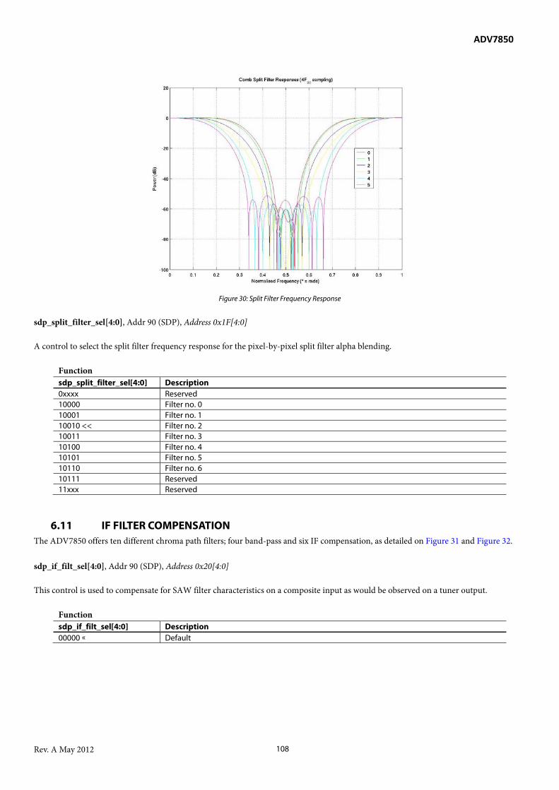
ADV7850
Rev. A May 2012 108
Figure 30: Split Filter Frequency Response
sdp_split_filter_sel[4:0], Addr 90 (SDP), Address 0x1F[4:0] A control to select the split filter frequency response for the pixel-by-pixel split filter alpha blending.
Function sdp_split_filter_sel[4:0] Description 0xxxx Reserved 10000 Filter no. 0 10001 Filter no. 1 10010 << Filter no. 2 10011 Filter no. 3 10100 Filter no. 4 10101 Filter no. 5 10110 Filter no. 6 10111 Reserved 11xxx Reserved
6.11 IF FILTER COMPENSATION The ADV7850 offers ten different chroma path filters; four band-pass and six IF compensation, as detailed on Figure 31 and Figure 32. sdp_if_filt_sel[4:0], Addr 90 (SDP), Address 0x20[4:0] This control is used to compensate for SAW filter characteristics on a composite input as would be observed on a tuner output.
Function sdp_if_filt_sel[4:0] Description 00000 Default
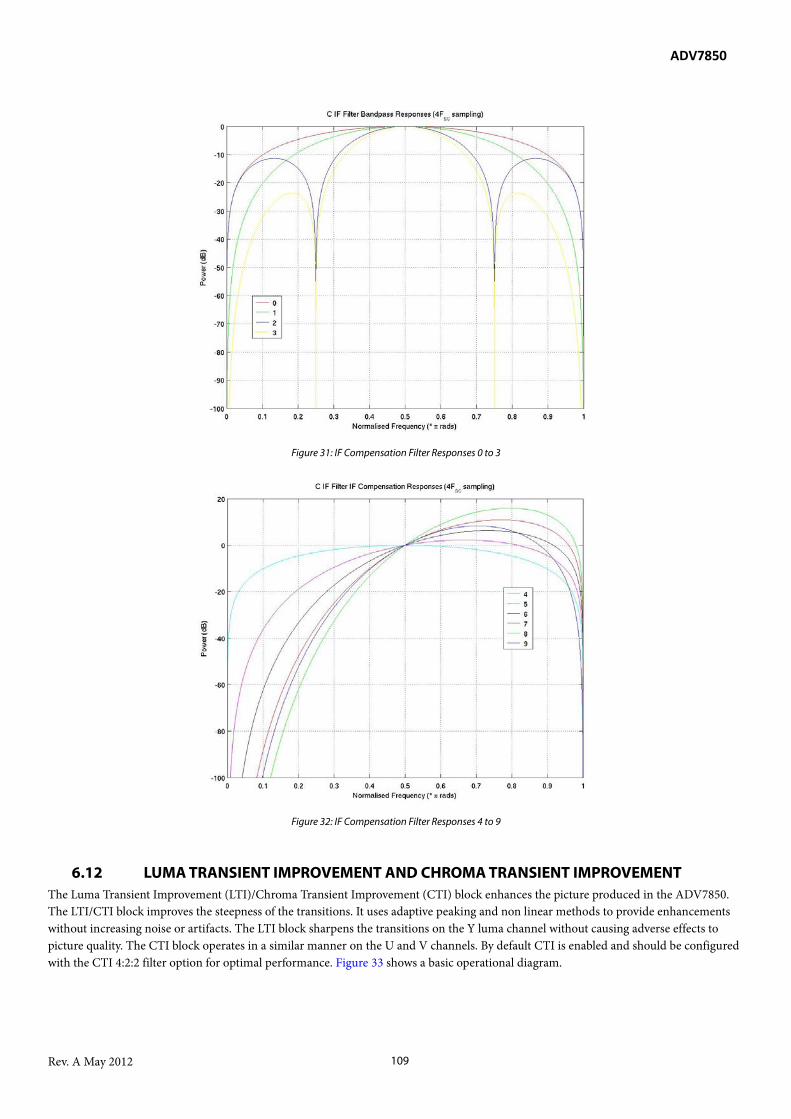
ADV7850
Rev. A May 2012 109
Figure 31: IF Compensation Filter Responses 0 to 3
Figure 32: IF Compensation Filter Responses 4 to 9
6.12 LUMA TRANSIENT IMPROVEMENT AND CHROMA TRANSIENT IMPROVEMENT The Luma Transient Improvement (LTI)/Chroma Transient Improvement (CTI) block enhances the picture produced in the ADV7850. The LTI/CTI block improves the steepness of the transitions. It uses adaptive peaking and non linear methods to provide enhancements without increasing noise or artifacts. The LTI block sharpens the transitions on the Y luma channel without causing adverse effects to picture quality. The CTI block operates in a similar manner on the U and V channels. By default CTI is enabled and should be configured with the CTI 4:2:2 filter option for optimal performance. Figure 33 shows a basic operational diagram.

ADV7850
Rev. A May 2012 110
Figure 33: LTI/CTI Operation Diagram
sdp_lti_en, Addr 90 (SDP), Address 0x0E[1] This control is used to enable Luma Transient Improvement (LTI).
Function sdp_lti_en Description 1 Enable LTI 0 Disable LTI
sdp_cti_en, Addr 90 (SDP), Address 0x0E[0] This control is used to enable Chroma Transient Improvement (CTI).
Function sdp_cti_en Description 1 Enable CTI 0 Disable CTI
sdp_scm_cti_en, Addr 90 (SDP), Address 0x0E[5] This control is used to enable CTI in SECAM modes.
Function sdp_scm_cti_en Description 1 Enable extra CTI in SECAM modes 0 Disable extra CTI in SECAM modes
The sdp_scm_cti_en bit enables an independent CTI block for SECAM modes. The SECAM signal is often clipped because of the LF-emphasis filter that is used on the transmitter side. Once a signal is restored on the receiver side, its chroma transitions are slower.
LTI/CTI
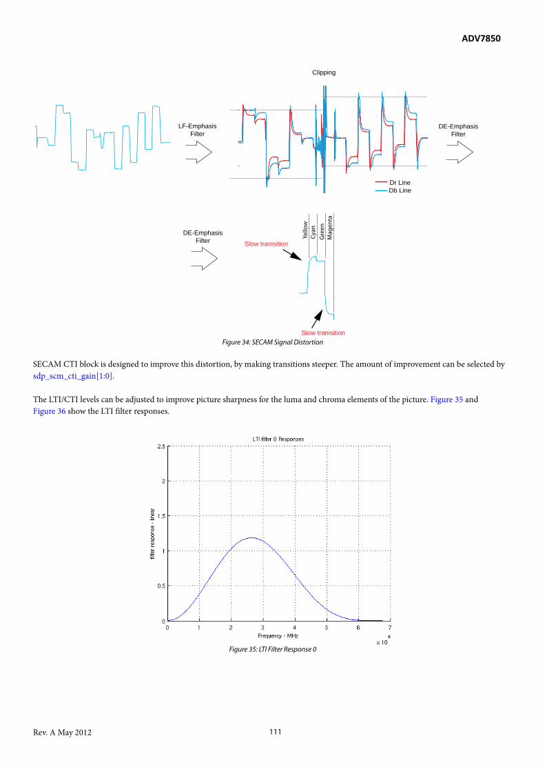
ADV7850
Rev. A May 2012 111
Figure 34: SECAM Signal Distortion
SECAM CTI block is designed to improve this distortion, by making transitions steeper. The amount of improvement can be selected by sdp_scm_cti_gain[1:0]. The LTI/CTI levels can be adjusted to improve picture sharpness for the luma and chroma elements of the picture. Figure 35 and Figure 36 show the LTI filter responses.
Figure 35: LTI Filter Response 0
LF-EmphasisFilter
DE-EmphasisFilter
Clipping
Slow tranisition
Slow tranisition
Yello
wCy
anG
reen
Mag
enta
DE-EmphasisFilter
Dr LineDb Line

ADV7850
Rev. A May 2012 112
Figure 36: LTI Filter Response 1
sdp_lti_level[6:0], Addr 90 (SDP), Address 0x25[6:0] This control is used to set the amount of LTI applied. A larger value corresponds to the sharpening of luma transients.
Function sdp_lti_level[6:0] Description Bigger values More sharpening of luma transients 0 No transient improvement
sdp_cti_level[5:0], Addr 90 (SDP), Address 0x26[5:0] This control is used to set the amount of CTI applied. A larger value corresponds to the sharpening of chroma transients.
Function sdp_cti_level[5:0] Description Bigger values More sharpening of chroma transients 0 No transient improvement
sdp_scm_cti_gain[1:0], Addr 90 (SDP), Address 0x28[2:1] This control is used to change the gain used for CTI (SECAM modes).
Function sdp_scm_cti_gain[1:0] Description 0 *0.125 1 *0.25 2 *0.375 3 *0.5
The LTI/CTI block allows the user to select between two filter responses. Figure 37 and Figure 38 illustrate filter response 0 and filter response 1 for CTI.

ADV7850
Rev. A May 2012 113
Figure 37: CTI Filter Response 0
Figure 38: CTI Filter Response 1
sdp_lti_filt_sel, Addr 90 (SDP), Address 0x25[7] This control is used to select one of two filter responses available in LTI operation.
Function sdp_lti_filt_sel Description 1 Select filter response 1 as part of LTI 0 Select filter response 0 as part of LTI
sdp_cti_filt_sel, Addr 90 (SDP), Address 0x26[7] This control is used to select one of two filter responses available for CTI operation.

ADV7850
Rev. A May 2012 114
Function sdp_cti_filt_sel Description 1 Select filter response 1 as part of CTI 0 Select filter response 0 as part of CTI
sdp_cti_filt_sel_422, Addr 90 (SDP), Address 0x26[6] This control is used to select the filter of high gain for 422 CTI data operation.
Function sdp_cti_filt_sel_422 Description 0 Select filter response with gain double 1 Select filter response for optimum 422 operation
The LTI/CTI flip registers allow the user to set a threshold on the filtered signal amplitude. Above this threshold, no LTI/CTI edge enhancements are applied. Adjusting this range allows LTI/CTI to be applied to mid to high range frequencies. sdp_lti_flip[1:0], Addr 90 (SDP), Address 0x27[3:2] This control is used to select the amplitude of the filtered input signal. Amplitudes above this threshold receive no LTI edge enhancement.
Function sdp_lti_flip[1:0] Description 00 128 01 512 10 1024 11 4096
sdp_cti_flip[1:0], Addr 90 (SDP), Address 0x27[7:6] This control is used to select the amplitude of the filtered input signal. Amplitudes above this threshold receive no CTI edge enhancement.
Function sdp_cti_flip[1:0] Description 00 128 01 512 10 1024 11 4096
6.13 RINGING REDUCTION The ADV7850 incorporates a ringing reduction block. This block is used to reduce ringing artifacts that can appear around sharp edges. There are two controls to use a ringing reduction block. sdp_ring_red_en enables a block, and sdp_ring_red_level[6:0] sets the level of reduction applied to the signal. sdp_ring_red_en, Addr 94 (sdp_IO), Address 0x51[7] This control is used to enable the ringing reduction block to remove a ringing artifact from around sharp edges.
Function sdp_ring_red_en Description 0 << Disable ringing reduction block 1 Enable ringing reduction block

ADV7850
Rev. A May 2012 115
sdp_ring_red_level[6:0], Addr 94 (sdp_IO), Address 0x51[6:0] This control is used to provide level control for the ringing reduction algorithm. Higher values give a more dramatic ringing reduction.
Function sdp_ring_red_level[6:0] Description 0000000 << No ringing reduction
6.14 HORIZONTAL AND VERTICAL PEAKING The ADV7850 offers horizontal and vertical luma peaking to enhance the picture produced by the decoder. The luma peaking function operates to boost or attenuate the mid to high frequency component of the Y signal. In horizontal and vertical peaking, the input is passed through a high-pass or band-pass filter. The input is cored and gained before it is added to/subtracted from the original signal. This ensures that all the information in the input signal is preserved. sdp_h_pk_inv and sdp_v_pk_inv determine whether the result is added to or subtracted from the input signal. The horizontal and vertical peaking controls are described in Section 6.14.1 and Section 6.14.2.
Figure 39: Peaking Block Diagram
6.14.1 Horizontal Peaking Horizontal peaking contains several controls that are described in this section. sdp_h_pk_en is the main control that enables or disables horizontal peaking. sdp_y_2d_pk_en is an additional control to enable or disable the horizontal peaking filter on the 2D combed output. sdp_h_pk_gain[3:0], in conjunction with sdp_h_pk_inv, sets the gain of the output. This is in a range of -1 to 0 (if sdp_h_pk_inv is set to 1) or 0 to 4 (if sdp_h_pk_inv is set to 0). sdp_h_pk_band[1:0] sets the band of horizontal peaking. sdp_h_pk_core[2:0] is the last control used to set the threshold of the output, below which no high frequency is added back to the input, as shown in Figure 40.
Filter Core Gain +
-
HFInput
Filter Core Gain +
-
HFInput
Horizontal Peaking
Vertical Peaking
0
1
SDP_H_PK_INV
0
1
SDP_V_PK_INV
Y-output
Y-output
SignalLimiting

ADV7850
Rev. A May 2012 116
Figure 40: Core Threshold in Horizontal Peaking
sdp_h_pk_en, Addr 90 (SDP), Address 0x0E[2] This control is used to enable the horizontal peaking filter. This is a universal peaking control applied after 2D/3D mixing. It is applied whether or not 3D has been enabled.
Function sdp_h_pk_en Description 1 Enable horizontal peaking 0 Disable horizontal peaking
sdp_y_2d_pk_en, Addr 90 (SDP), Address 0x0E[4] This control is used to enable the horizontal peaking filter on the 2D combed output. This peaking filter is applied to the 2D portion of the image before it is mixed with the 3D. It is important to note that it will always be applied to the 2D portion regardless of whether or not 3D comb is enabled. The purpose of this control is that where 3D comb is enabled, 2D peaking reduces the sharpness/resolution difference perceived in areas where motion occurs. 3D areas are always very sharp due to temporal comb; 2D areas need to be peaked to compensate for softness of 2D/1D separation.
Function sdp_y_2d_pk_en Description 1 Enable horizontal peaking 0 Disable horizontal peaking
sdp_h_pk_inv, Addr 90 (SDP), Address 0x22[7] This control is used to enable an inverse horizontal peaking filter operation.
Function sdp_h_pk_inv Description 1 Inverse peaking (attenuate HF) 0 Normal (gain HF)
sdp_h_pk_band[1:0], Addr 90 (SDP), Address 0x24[1:0] This control is used to set a horizontal peaking filter band.
Enhancing Output
Filtered Input
Core Threshold
Core Threshold

ADV7850
Rev. A May 2012 117
Function sdp_h_pk_band[1:0] Description 0 No filtering 1 Highpass 2 Bandpass peaking 3 Alternative bandpass peaking
Figure 41: Horizontal Peaking High-Pass Filter
Figure 42: Horizontal Peaking Band-Pass Filter 1

ADV7850
Rev. A May 2012 118
Figure 43: Horizontal Peaking Band-Pass Filter 2
sdp_h_pk_core[2:0], Addr 90 (SDP), Address 0x22[2:0] This control is used to select the horizontal threshold from the eight possible values listed in the following table. If the filtered output is less than the coring threshold, no high frequency is added back to the input. If the filter output is greater than the core threshold, it is passed through unchanged to the next stage.
Function sdp_h_pk_core[2:0] Description 000 0 001 8 010 16 011 24 100 32 101 40 110 48 111 56
sdp_h_pk_gain[3:0], Addr 90 (SDP), Address 0x22[6:3] This control is used to adjust the gain of the horizontal peaking filter. The peaking filter can visually improve the picture by showing more definition on the picture details that contain frequency components around 3 MHz. The filter response is also user selectable using the sdp_h_pk_band and sdp_h_pk_inv. It has a range of 0 to 4 or 0 to -4 depending on sdp_h_pk_inv.
Function sdp_h_pk_gain[3:0] Description 0100 Default gain
Plots of the filter responses are shown in Figure 41 to Figure 43.
6.14.2 Vertical Peaking Vertical peaking contains several controls, which are described in this section. sdp_v_pk_en is the main control that enables or disables vertical peaking.

ADV7850
Rev. A May 2012 119
sdp_v_pk_flip[2:0] with sdp_v_pk_clip[1:0] are used to set the maximum amount of enhancement that can be added before the gain is applied. sdp_v_pk_flip[2:0] sets the maximum amount of enhancement. Above this value, the amount of enhancement is reduced. sdp_v_pk_clip[1:0] is a control that is applied after sdp_v_pk_flip[2:0]. It sets the positive and negative values of saturation. This mechanism is explained in Figure 44. sdp_v_pk_core[2:0] is the another control that is used to set the threshold of the output before applying it to gain block, below which values are cored to 0. Refer to Figure 44. sdp_v_pk_gain[3:0] in conjunction with sdp_v_pk_inv sets the gain of the output that can be in the ranges of -1 to 0 (if sdp_v_pk_inv is set to 1) or 0 to 4 (if sdp_v_pk_inv is set to 0).
Figure 44: Peaking Controls
sdp_v_pk_en, Addr 90 (SDP), Address 0x0E[3] This control is used to enable the vertical peaking filter.
Function sdp_v_pk_en Description 1 Enable vertical peaking 0 Disable vertical peaking
sdp_v_pk_inv, Addr 90 (SDP), Address 0x23[7] This control is used to enable an inverse vertical peaking filter operation.
Function sdp_v_pk_inv Description 1 Inverse peaking (attenuate HF) 0 Normal (gain HF)
sdp_v_pk_gain[3:0], Addr 90 (SDP), Address 0x23[6:3] This control is used to adjust the gain for the vertical peaking filter. The user can select to boost or attenuate the mid region of the Y spectrum around 3 MHz. The peaking filter can visually improve the picture by showing more definition on the picture details that contain frequency components around 3 MHz. It is to be used in conjunction with an sdp_v_pk_inv range of 0 to 4 or 0 to -4, depending on sdp_v_pk_inv.
Function sdp_v_pk_gain[3:0] Description 0010 Default gain
Enhancing Output
Flip Threshold
Clip Threshold
Flip Threshold/2
Filtered Input
Core Threshold
Flip Threshold/2
Clip Threshold
Core Threshold
Flip Threshold
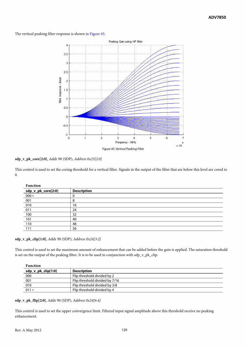
ADV7850
Rev. A May 2012 120
The vertical peaking filter response is shown in Figure 45.
Figure 45: Vertical Peaking Filter
sdp_v_pk_core[2:0], Addr 90 (SDP), Address 0x23[2:0] This control is used to set the coring threshold for a vertical filter. Signals in the output of the filter that are below this level are cored to 0.
Function sdp_v_pk_core[2:0] Description 000 0 001 8 010 16 011 24 100 32 101 40 110 48 111 56
sdp_v_pk_clip[1:0], Addr 90 (SDP), Address 0x24[3:2] This control is used to set the maximum amount of enhancement that can be added before the gain is applied. The saturation threshold is set on the output of the peaking filter. It is to be used in conjunction with sdp_v_pk_clip.
Function sdp_v_pk_clip[1:0] Description 000 Flip threshold divided by 2 001 Flip threshold divided by 7/16 010 Flip threshold divided by 3/8 011 Flip threshold divided by 4
sdp_v_pk_flip[2:0], Addr 90 (SDP), Address 0x24[6:4] This control is used to set the upper convergence limit. Filtered input signal amplitude above this threshold receive no peaking enhancement.

ADV7850
Rev. A May 2012 121
Function sdp_v_pk_flip[2:0] Description 000 64 001 128 010 256 011 512 100 1024 101 2048 110 3072 111 4095
6.15 FRAME SYNCHRONIZATION (FRAME TIME BASE CORRECTION) The frame synchronizer block in the ADV7850 provides stable timing information and stable clock frequency in the event of irregularities on the input signal. These irregularities include items such as VCR head switches, extra lines in a frame, too few lines in a frame, non standard input frequency, or interrupted field sequence that occur during VCR trick mode inputs and during input channel changes. Nominal 480i/576i H/V/F and/or CCIR-656 type timing and data is output from the system under all conditions. Figure 46 provides a block diagram for the system.
Figure 46: Frame Synchronization Block Diagram
Input video is decoded in the decoder core to component YPrPb (or equivalent) with associated HSync, VSync, and field signals. The time base correction (TBC) control block writes YPrPb data to the frame memories in the external SDRAM. The TBC control block synthesizes H, V, and F timing signals with nominal 480i/576i timing and reads YUV data from the frame memories based on nominal timing signals generated using a fixed frequency clock. This fixed frequency clock is also used to clock data out of the ADV7850. The fixed frequency clock is user programmable but is intended to operate at 13.5 MHz, 27 MHz, or 54 MHz depending on the chosen output format. The external SDRAM memory is used to provide storage for fields of data. The frame synchronization controls are described below. sdp_fr_tbc_en, Addr 90 (SDP), Address 0x12[2] This control is used to enable frame Time Based Correction (TBC).
Function sdp_fr_tbc_en Description 1 Enable frame TBC 0 Disable frame TBC
External DDR RAM
TBC Control
Video Data and Decoded
H, V, F Timing (Decoded from
Input)
Output Video (H,V,F/CCIR56
Nominal Timing)
YPbPr data
Decoded H/V/F
YPbPr data
Nominal H/V/F Core clk and dv
YPbPr data
Nominal H,V,F
Fixed freq output clk
DDS Clock Generator
(I2C programmable
fixed frequency)
ADV7850
Rev. A May 2012 122
sdp_tbc_en, Addr 90 (SDP), Address 0x34[7] This control is used to enable line TBC. When enabled, it only becomes active in VCR trick modes.
Function sdp_tbc_en Description 1 Enable line TBC (time base correction) 0 Disable line TBC (time base correction)
sdp_freeze_frame, Addr 94 (sdp_IO), Address 0x6F[1] This control is used to continuously loop out a frame of video data from the TBC block. This feature will effectively allow the image to be paused on screen. When this bit is set, new data will not be updated into the Frame memory. This bit is only valid when Frame TBC is enabled.
Function sdp_freeze_frame Description 0 << Do not freeze Frame TBC input 1 Freeze Frame TBC input
6.16 FREE RUN MODE Free Run mode in the SDP Core is designed to provide a stable clock and predictable video when no signal is applied to an input or if a signal cannot be decoded. The ADV7850 can automatically activate Free Run mode when sdp_free_run_auto is set to 1. Free run mode can be also forced by sdp_force_free_run regardless of the input state. Free Run mode controls default color insertion and causes ADV7850 to generate a default clock. The state in which this happens can be monitored via the sdp_free_run readback. The default color of Free Run mode can be set by the following registers:
• sdp_free_run_man_col_en • sdp_free_run_y[7:0] • sdp_free_run_u[3:0] • sdp_free_run_v[3:0]
ADV7850 can also output color bars instead of flat picture. To do this, sdp_free_run_cbar_en should be set to 1. sdp_free_run_auto, Addr 90 (SDP), Address 0xDD[3] This control is used to enable automatic free run operation. The part enters free run if no valid input video is detected.
Function sdp_free_run_auto Description 1 Free run if no valid input video detected 0 Do not free run even if no valid input video detected
sdp_free_run_man_col_en, Addr 90 (SDP), Address 0xDD[2] This control is used to enable the manual setting of video data output in video mode. If in free run, luma and chroma values are set by sdp_free_run_y, sdp_free_run_v, and sdp_free_run_u.

ADV7850
Rev. A May 2012 123
Function sdp_free_run_man_col_en
Description
1 If in free run, output manual luma and chroma values set by sdp_free_run_y, sdp_free_run_v, and sdp_free_run_u
0 If in free run, output decoded video data sdp_free_run_cbar_en, Addr 90 (SDP), Address 0xDD[1] This control is used to select the color bar pattern to be output in manual free run mode.
Function sdp_free_run_cbar_en Description 1 If in free run mode, output color bar data 0 If in free run mode, output free run mode data
sdp_force_free_run, Addr 90 (SDP), Address 0xDD[0] This control is used to force free run mode irrespective of the input lock status.
Function sdp_force_free_run Description 1 Force free run 0 Normal operation
sdp_free_run_y[7:0], Addr 90 (SDP), Address 0xDE[7:0] This control is used to set the luma level to output in free run mode if sdp_free_run_man_col_en is set to 1. sdp_free_run_v[3:0], Addr 90 (SDP), Address 0xDF[7:4] This control is used to set the V level to output in free run mode if sdp_free_run_man_col_en is set to 1. sdp_free_run_u[3:0], Addr 90 (SDP), Address 0xDF[3:0] This control is used to set the U level to output in free run mode if sdp_free_run_man_col_en is set to 1.
6.17 LETTERBOX DETECTION Incoming video signals can conform to different aspect ratios (16:9 wide screen of 4:3 standard). For transmissions in the wide screen format, a digital sequence (WSS) is transmitted with the video signal. If a WSS sequence is provided, the aspect ratio of the video can be derived from digitally decoded bits contained within it. In the absence of a WSS sequence, the letterbox detection can be used to find wide screen signals. The detection algorithm examines the active video content of lines at the start and at the end of a field. If the presence of black lines is detected, this can serve as an indication that the currently shown picture is in wide screen format. The active video content (luminance magnitude) over a line of video is summed together. At the end of a line, this accumulated value is compared to a threshold and a decision is made whether or not a particular line is considered to be black. The threshold value needed can depend on the type of input signal, and some control is provided via sdp_lbox_thr[4:0].

ADV7850
Rev. A May 2012 124
sdp_lbox_thr[4:0], Addr 90 (SDP), Address 0xDC[4:0] This control is used to set the threshold for black line detection in letterbox detection. A larger value increases the possibility of detecting a line as black.
Function sdp_lbox_thr[4:0] Description 00010 Default threshold for detection of black lines
sdp_lbox_blk_lvl[2:0], Addr 90 (SDP), Address 0xDC[7:5] This control is used to set the expected blank level in the lbox detection block. A larger value corresponds to a higher blank level.
Function sdp_lbox_blk_lvl[2:0] Description 000 None 001 None 010 None 011 None 100 None 101 None 110 None 111 None
6.17.1 Detection at Start of Field The ADV7850 expects a section of at least six consecutive black lines of video at the top of a field. Once those lines are detected, sdp_lbox_blk_top[7:0] reports back the number of black lines actually found. By default, the ADV7850 starts looking for those black lines in synchronization with the beginning of active video, for example, straight after the last VBI video line. sdp_lbox_beg_del[3:0] allows the user to set the start of letterbox detection from the beginning of a frame on a line by line basis. The detection window closes in the middle of the field.
6.17.2 Detection at End of Field The ADV7850 expects at least six continuous lines of black video at the bottom of a field before reporting back the number of lines actually found via the sdp_lbox_blk_bot[7:0] value. The activity window for the letterbox detection (end of field) starts in the middle of the active field. Its end is programmable via sdp_lbox_end_del[3:0].
6.17.3 Detection at Mid Range Some transmissions of wide screen video include subtitles within the lower black box. If the ADV7850 finds at least two black lines, followed by some more non black video (for example, the subtitle), and finally followed by the remainder of the bottom black block, it reports back a mid count via sdp_lbox_blk_sub_bot[7:0]. Note: There is a two field delay in the reporting of any line count parameters. There is no letterbox detected bit. The user is requested to read the sdp_lbox_blk_top[7:0] and sdp_lbox_blk_sub_bot[7:0] values, and come to a conclusion about the presence of letterbox type video in the software. sdp_lbox_blk_top[7:0], SDP Map, Address 0x4C, [7:0] sdp_lbox_blk_bot[7:0], SDP Map, Address 0x4D, [7:0] sdp_lbox_blk_sub_bot[7:0], SDP Map, Address 0x4E, [7:0]
Access Information Signal Name Address Default Description sdp_lbox_blk_top[7:0] 0x4C Read back only Number of black lines detected at top of field
sdp_lbox_blk_bot[7:0] 0x4D Read back only Number of black lines detected at bottom of field sdp_lbox_blk_sub_bot[7:0] 0x4E Read back only Number of black lines detected at bottom of field
(including subtitle lines)

ADV7850
Rev. A May 2012 125
sdp_lbox_beg_del[3:0], Addr 90 (SDP), Address 0xDB[3:0] This control is used to set the letterbox detection begin line versus the default position.
Function sdp_lbox_beg_del[3:0] Description 1000 Letterbox detection aligned with start line of active video. Window starts after VBI data line.
sdp_lbox_end_del[3:0], Addr 90 (SDP), Address 0xDB[7:4] This control is used to set the letterbox detection end line versus the default position.
Function sdp_lbox_end_del[3:0] Description 1000 Letterbox detection ends with last active line of video on field
6.18 SDP SYNCHRONIZATION OUTPUT SIGNALS
6.18.1 HSync Timing Configuration The following controls allow the user to configure the behavior of the HSync on the output pin only: HSync timing adjustments:
• sdp_hs_beg_adj[11:0] • sdp_hs_width[11:0] • sdp_fhe_tog_inv • sdp_fho_tog_inv
HSync polarity adjustment:
• sdp_hs_pol sdp_hs_pol, Addr 94 (sdp_IO), Address 0xB1[0] A control to change polarity of HS/CS.
Function sdp_hs_pol Description 0 Inverted HS/CS pin polarity 1 << Default HS/CS pin polarity
sdp_hs_beg_adj[11:0], Addr 94 (sdp_IO), Address 0x94[3:0]; Address 0x95[7:0] The sdp_hs_beg_adj[11:0] and sdp_hs_width[11:0] bits allow the user to freely position the HSync signal applied to the output pin within the video line. The values in the sdp_hs_beg_adj[11:0] and sdp_hs_width[11:0] bits are measured in pixel units from the default falling edge position of the HSync. Using both values, the user can program both the position and the width of the HSync output signal. The sdp_hs_beg_adj[11:0] adjusts the leading and trailing edge positions, hence adjusting the HSync pulse. The number applied to the register offsets the HSync pulse position with respect to the default value. The number is a twos complement value, which allows both positive and negative edge movement.
Function sdp_hs_beg_adj[11:0] Description 0x000 << Default value

ADV7850
Rev. A May 2012 126
sdp_hs_width[11:0], Addr 94 (sdp_IO), Address 0x96[3:0]; Address 0x97[7:0] The sdp_hs_width[11:0] bits allow the user to freely adjust the width of the HSync pulse within the video line. The values in the sdp_hs_width[11:0] bits are measured in pixel units from the falling edge of HSync. The position of this edge is controlled by placing an unsigned binary number into the sdp_hs_beg_adj[11:0] bits.
Function sdp_hs_width[11:0] Description 0x020 << Default value (unsigned control)
sdp_fhe_tog_inv, Addr 94 (sdp_IO), Address 0xB0[5] A control to swap switch position of field on even fields.
Function sdp_fhe_tog_inv Description 0 << Use default horizontal switch position for field on even fields 1 Swap horizontal switch position for field on even fields between beginning and middle of the
line sdp_fho_tog_inv, Addr 94 (sdp_IO), Address 0xB0[4] A control to swap switch position of field on odd fields.
Function sdp_fho_tog_inv Description 0 << Use default horizontal switch position for field on odd fields 1 Swap horizontal switch position for field on odd fields between beginning and middle of the
line
Figure 47: HSync and VSync Timing Controls
6.18.2 VSync and FIELD Configuration The following controls allow the user to configure the behavior of the VSync and FIELD signal on the output pins VS/FIELD and

ADV7850
Rev. A May 2012 127
FIELD/DE: • Polarity pin adjustments:
sdp_vs_pol sdp_fld_pol
• VSync timing adjustments relative to HSync: sdp_vsf_h_beg_adj[11:0] sdp_vsf_h_mid_adj[11:0]
• VSync timing adjustments: sdp_vs_v_beg_o_adj[5:0] sdp_vs_v_beg_e_adj[5:0] sdp_vs_v_end_o_adj[5:0] sdp_vs_v_end_e_adj[5:0] sdp_vho_beg_inv sdp_vho_end_inv sdp_vhe_beg_inv sdp_vhe_end_inv
sdp_vs_pol, Addr 94 (sdp_IO), Address 0xB1[1] A control to change polarity of VS/FIELD.
Function sdp_vs_pol Description 0 << Default VS/FIELD pin polarity 1 Inverted VS/FIELD pin polarity
sdp_fld_pol, Addr 94 (sdp_IO), Address 0xB1[2] A control to change polarity of FIELD/DE.
Function sdp_fld_pol Description 0 Inverted FIELD/DE pin polarity 1 << Default FIELD/DE pin polarity
sdp_vsf_h_beg_adj[11:0], Addr 94 (sdp_IO), Address 0x9C[3:0]; Address 0x9D[7:0] The sdp_vsf_h_beg_adj[11:0] bits adjust the VS/FIELD output relative to the HSync position. The values are measured in pixel units from the falling edge of HSync. This control is used when the VSync and Field outputs are coincident with HSync. The position of the VSync and Field relative to the HSync is controlled by placing a two’s complement number into the sdp_vsf_h_beg_adj[11:0] bits.
Function sdp_vsf_h_beg_adj[11:0]
Description
0x000 << Default value sdp_vsf_h_mid_adj[11:0], Addr 94 (sdp_IO), Address 0x9E[3:0]; Address 0x9F[7:0] The sdp_vsf_h_mid_adj[11:0] bits adjust the SDP VS/FIELD output relative to the HSync position within the video line. The values are measured in pixel units from the falling edge of HSync. This control is used when the VSync or Field changes approximately midway between HSyncs. The position of the VSync and Field relative to the HSync is controlled by placing a twos complement number into the sdp_vsf_h_mid_adj[11:0] bits.

ADV7850
Rev. A May 2012 128
Function sdp_vsf_h_mid_adj[11:0]
Description
0x000 << Default value sdp_vs_v_beg_o_adj[5:0], Addr 94 (sdp_IO), Address 0xA8[5:0] Adjust SDP VSync pin begin line relative to default, only +ve recommended, twos complement.
Function sdp_vs_v_beg_o_adj[5:0]
Description
000100 << Default value sdp_vs_v_beg_e_adj[5:0], Addr 94 (sdp_IO), Address 0xA9[5:0] Adjust SDP VSync pin begin line relative to default, only +ve recommended, 2s complement.
Function sdp_vs_v_beg_e_adj[5:0]
Description
000100 << Default value sdp_vs_v_end_o_adj[5:0], Addr 94 (sdp_IO), Address 0xAA[5:0] Adjust SDP VSync pin end line relative to default, only +ve recommended, 2s complement.
Function sdp_vs_v_end_o_adj[5:0]
Description
000100 << Default value sdp_vs_v_end_e_adj[5:0], Addr 94 (sdp_IO), Address 0xAB[5:0] Adjust SDP VSync pin end line relative to default, only +ve recommended, 2s complement.
Function sdp_vs_v_end_e_adj[5:0]
Description
000100 << Default value sdp_fld_tog_o_adj[5:0], Addr 94 (sdp_IO), Address 0xA6[5:0] Adjust SDP field pin transition relative to default, only +ve recommended, 2s complement.
Function sdp_fld_tog_o_adj[5:0] Description 000100 << Default value
sdp_fld_tog_e_adj[5:0], Addr 94 (sdp_IO), Address 0xA7[5:0] Adjust SDP field pin transition relative to default, only +ve recommended, 2s complement.
ADV7850
Rev. A May 2012 129
Function sdp_fld_tog_e_adj[5:0] Description 000100 << Default value
sdp_vho_beg_inv, Addr 94 (sdp_IO), Address 0xB0[0] A control to swap switch position of field and beginning of VSync on odd fields.
Function sdp_vho_beg_inv Description 0 << Use default horizontal switch position for field and beginning of VSync on odd fields 1 Swap horizontal switch position for field and beginning of VSync on odd fields between
beginning and middle of the line sdp_vhe_beg_inv, Addr 94 (sdp_IO), Address 0xB0[1] A control to swap switch position of field and beginning of VSync on even fields.
Function sdp_vhe_beg_inv Description 0 << Use default horizontal switch position for field and beginning of VSync on eve fields 1 Swap horizontal switch position for field and beginning of VSync on even fields between
beginning and middle of the line sdp_vho_end_inv, Addr 94 (sdp_IO), Address 0xB0[2] A control to swap switch position of field and end of VSync on odd fields.
Function sdp_vho_end_inv Description 0 << Use default horizontal switch position for field and end of VSync on odd fields 1 Swap horizontal switch position for field and end of VSync on odd fields between beginning
and middle of the line sdp_vhe_end_inv, Addr 94 (sdp_IO), Address 0xB0[3] A control to swap switch position of field and end of VSync on even fields.
Function sdp_vhe_end_inv Description 0 << Use default horizontal switch position for field and end of VSync on even fields 1 Swap horizontal switch position for field and end of VSync on even fields between beginning
and middle of the line
6.18.3 DE Configuration The following controls allow the user to configure the behavior of the DE signal on the output pin:
• DE polarity adjustment: sdp_de_pol
• DE timing adjustments relative to VSync: sdp_de_v_beg_o_adj[5:0] sdp_de_v_beg_e_adj[5:0] sdp_de_v_end_o_adj[5:0] sdp_de_v_end_e_adj[5:0]
• DE timing adjustments relative to HSync: sdp_de_h_beg_adj[11:0]

ADV7850
Rev. A May 2012 130
sdp_de_h_end_adj[11:0] sdp_de_pol, Addr 94 (sdp_IO), Address 0xB1[4] A control to change polarity of DE.
Function sdp_de_pol Description 0 Inverted DE polarity 1 << Default DE polarity
sdp_de_v_beg_o_adj[5:0], Addr 94 (sdp_IO), Address 0xAC[5:0] Adjust SDP DE pin begin line relative to default, only +ve recommended, 2s complement.
Function sdp_de_v_beg_o_adj[5:0]
Description
000100 << Default value sdp_de_v_beg_e_adj[5:0], Addr 94 (sdp_IO), Address 0xAD[5:0] Adjust SDP DE pin begin line relative to default, only +ve recommended, 2s complement.
Function sdp_de_v_beg_e_adj[5:0]
Description
000100 << Default value sdp_de_v_end_o_adj[5:0], Addr 94 (sdp_IO), Address 0xAE[5:0] Adjust SDP DE pin end line relative to default, only +ve recommended, 2s complement.
Function sdp_de_v_end_o_adj[5:0]
Description
000100 << Default value sdp_de_v_end_e_adj[5:0], Addr 94 (sdp_IO), Address 0xAF[5:0] Adjust SDP DE pin end line relative to default, only +ve recommended, 2s complement.
Function sdp_de_v_end_e_adj[5:0]
Description
000100 << Default value sdp_de_h_beg_adj[11:0], Addr 94 (sdp_IO), Address 0x98[3:0]; Address 0x99[7:0] Adjust SDP DE horizontal begin position versus default, 2s complement.
Function sdp_de_h_beg_adj[11:0]
Description
0x000 << Default value

ADV7850
Rev. A May 2012 131
sdp_de_h_end_adj[11:0] allows the user to adjust the horizontal DE trailing edge position relative to the HSync. The values are measured in pixel units from the falling edge of HSync. The position of the horizontal DE trailing edge is controlled by placing a twos complement number into the sdp_de_h_end_adj[11:0] bits. The number is a twos complement value that allows both positive and negative edge movement. sdp_de_h_end_adj[11:0], Addr 94 (sdp_IO), Address 0x9A[3:0]; Address 0x9B[7:0] Adjust SDP DE horizontal end position versus default, 2s complement.
Function sdp_de_h_end_adj[11:0]
Description
0x000 << Default value
Figure 48: DE Timing Controls
6.18.4 CSync Signal Configuration The sdp_cs_pol control allows the user to configure the polarity of the CSync signal on the output pin. sdp_cs_pol, Addr 94 (sdp_IO), Address 0xB1[3] A control to change polarity of HS/CS.
Function sdp_cs_pol Description 0 Inverted HS/CS polarity 1 << Default HS/CS polarity
SDP
_DE_
V_E
ND
_E_A
DJ
Active VideoEven Field
SDP_
DE_
V_E
ND
_O_A
DJ
SDP
_DE_
V_B
EG_E
_AD
JSD
P_D
E_V
_BEG
_O_A
DJ
Active VideoOdd Field

ADV7850
Rev. A May 2012 132
6.18.5 Manual Color Space Conversion Matrix The ADV7850 features Color Space Converter (CSC) in SDP core. CSC provides any-to-any color space conversion support, that is, it support formats such as RGB, YUV, YcrCb, and many other color spaces. The CSC matrix in the ADV7850 is a 3 x 3 matrix with full programmability of all coefficients in the matrix in manual mode. Each coefficient is 12-bit wide to ensure signal integrity is maintained in the CSC section. The CSC contains three identical processing channels, one of which is shown in Figure 49. The main inputs labeled In_A, In_B, and In_C comes from SDP core output. Each input to the individual channels to the CSC is multiplied by a separate coefficient for each channel. In Figure 49, these coefficients are marked A1, A2, and A3. The variable labeled A4 in Figure 49 is used as an offset control for channel A in the CSC. There is also a further CSC control bit labeled sdp_csc_scale; this bit can be used to accommodate coefficients that extend the supported range. The functional diagram for a single channel in the CSC as per Figure 49 is repeated for the other two remaining channels B and C. The coefficients for these channels are called B1, B2, B3, B4, C1, C2, C3, and C4. To enable the manual color space conversion matrix, the sdp_csc_auto bit should be set high.
Figure 49: Single CSC Channel
The coefficients mentioned previously are detailed in Table 12 along with the default values for these coefficients.
Table 12: CSC Coefficients
Function Bit sdp_IO Map Address Reset Value (Hex) Description sdp_a1[12:0] 0xE0[4:0], 0xE1[7:0] 0x07D2 Coefficients for channel A sdp_a2[12:0] 0xE2[4:0], 0xE3[7:0] 0x0000 sdp_a3[12:0] 0xE4[4:0], 0xE5[7:0] 0x0040 sdp_b1[12:0] 0xE8[4:0], 0xE9[7:0] 0x0000 Coefficients for channel B sdp_b2[12:0] 0xEA[4:0], 0xEB[7:0] 0x0926 sdp_b3[12:0] 0xEC[4:0], 0xED[7:0] 0x0000 sdp_c1[12:0] 0xF0[4:0], 0xF1[7:0] 0x0000 Coefficients for channel C sdp_c2[12:0] 0xF2[4:0], 0xF3[7:0] 0x0000 sdp_c3[12:0] 0xF4[4:0], 0xF5[7:0] 0x0681 sdp_csc_scale 0xE0[7] 0x00 Scaling for CSC formula sdp_a4[14:0] 0xE6[6:0], 0xE7[7:0] 0x7F00 Offsets for the three channels sdp_b4[14:0] 0xEE[6:0], 0xEF[7:0] 0x0000 sdp_c4[14:0] 0xF6[6:0], 0xF7[7:0] 0x0000
sdp_csc_auto, Addr 94 (sdp_IO), Address 0xE0[6] This control is used to select the CSC operation.
In_A [11:0]
In_C [11:0]
X
A1[12:0]
X
A2[12:0]
X
A3[12:0]
+ + +
A4[12:0]
In_B [11:0]
X 2
CSC_scale
Out_A [11:0]1
0

ADV7850
Rev. A May 2012 133
Function sdp_csc_auto Description 0 Use manual CSC coefficients 1 << Use automatic CSC coefficients
sdp_csc_scale, Addr 94 (sdp_IO), Address 0xE0[7] This control is used to set the CSC gain.
Function sdp_csc_scale Description 0 << CSC scaler set to 1 1 CSC scaler set to 2
This bit allows the control to accommodate coefficients that extend the supported range of the DPP. sdp_a1[12:0], Addr 94 (sdp_IO), Address 0xE0[4:0]; Address 0xE1[7:0] This control is used to set the CSC A1 coefficient for the SDP output color space converter.
Function sdp_a1[12:0] Description 0x07D2 << Default
sdp_a2[12:0], Addr 94 (sdp_IO), Address 0xE2[4:0]; Address 0xE3[7:0] This control is used to set the CSC A2 coefficient for the SDP output color space converter.
Function sdp_a2[12:0] Description 0x0000 << Default
sdp_a3[12:0], Addr 94 (sdp_IO), Address 0xE4[4:0]; Address 0xE5[7:0] This control is used to set the CSC A3 coefficient for the SDP output color space converter.
Function sdp_a3[12:0] Description 0x0040 << Default
sdp_a4[14:0], Addr 94 (sdp_IO), Address 0xE6[6:0]; Address 0xE7[7:0] This control is used to set the CSC A4 coefficient for the SDP output color space converter.
Function sdp_a4[14:0] Description 0x7F00 << Default
sdp_b1[12:0], Addr 94 (sdp_IO), Address 0xE8[4:0]; Address 0xE9[7:0] This control is used to set the CSC B1 coefficient for the SDP output color space converter.

ADV7850
Rev. A May 2012 134
Function sdp_b1[12:0] Description 0x0000 << Default
sdp_b2[12:0], Addr 94 (sdp_IO), Address 0xEA[4:0]; Address 0xEB[7:0] This control is used to set the CSC B2 coefficient for the SDP output color space converter.
Function sdp_b2[12:0] Description 0x0926 << Default
sdp_b3[12:0], Addr 94 (sdp_IO), Address 0xEC[4:0]; Address 0xED[7:0] This control is used to set the CSC B3 coefficient for the SDP output color space converter.
Function sdp_b3[12:0] Description 0x0000 << Default
sdp_b4[14:0], Addr 94 (sdp_IO), Address 0xEE[6:0]; Address 0xEF[7:0] This control is used to set the CSC B4 coefficient for the SDP output color space converter.
Function sdp_b4[14:0] Description 0x0000 << Default
sdp_c1[12:0], Addr 94 (sdp_IO), Address 0xF0[4:0]; Address 0xF1[7:0] This control is used to set the CSC C1 coefficient for the SDP output color space converter.
Function sdp_c1[12:0] Description 0x0000 << Default
sdp_c2[12:0], Addr 94 (sdp_IO), Address 0xF2[4:0]; Address 0xF3[7:0] This control is used to set the CSC C2 coefficient for the SDP output color space converter.
Function sdp_c2[12:0] Description 0x0000 << Default
sdp_c3[12:0], Addr 94 (sdp_IO), Address 0xF4[4:0]; Address 0xF5[7:0] This control is used to set the CSC C3 coefficient for the SDP output color space converter.
Function sdp_c3[12:0] Description 0x0681 << Default
sdp_c4[14:0], Addr 94 (sdp_IO), Address 0xF6[6:0]; Address 0xF7[7:0] This control is used to set the CSC C4 coefficient for the SDP output color space converter.

ADV7850
Rev. A May 2012 135
Function sdp_c4[14:0] Description 0x0000 << Default
6.18.5.1 CSC Manual Programming This section outlines the settings for a conversion from NTSC YCrCb to RGB output. The CSC is only supported in these fixed settings: 94 97 00 HSync width Adjustment 94 B2 60 Disable AV codes 94 B0 00 Disable H and v blanking 94 E0 83 Manual CSC mode 94 E1 A7 CSC coefficient 94 E2 1E CSC coefficient 94 E3 91 CSC coefficient 94 E4 1D CSC coefficient 94 E5 E2 CSC coefficient 94 E6 7D CSC coefficient 94 E7 00 CSC coefficient 94 E8 03 CSC coefficient 94 E9 A7 CSC coefficient 94 EA 07 CSC coefficient 94 EB 61 CSC coefficient 94 EC 00 CSC coefficient 94 ED 00 CSC coefficient 94 EE 79 CSC coefficient 94 EF 00 CSC coefficient 94 F0 03 CSC coefficient 94 F1 A7 CSC coefficient 94 F2 00 CSC coefficient 94 F3 00 CSC coefficient 94 F4 04 CSC coefficient 94 F5 29 CSC coefficient 94 F6 79 CSC coefficient 94 F7 00 CSC coefficient

ADV7850
Rev. A May 2012 136
7 HDMI RECEIVER
Figure 50: Functional Block Diagram of HDMI Core
7.1 MODES OF OPERATION The ADV7850 can operate in two modes
• HDMI Mux Mode • HDMI Non-Mux Mode
7.1.1 HDMI Mux Mode In HDMI Mux mode the HDMI data is passed directly from the RX to the TX. In this mode the ADV7850 supports up to 3GHz inputs. All the InfoFrame data is automatically passed to the HDMI TX within the ADV7850 and output directly to the backend IC.
• STDI is available in this mode • Format Detection is available • AVI InfoFrame monitoring is available • Audio Extraction is available in this mode
7.1.2 HDMI Non-Mux Mode In HDMI Non-Mux mode, the HDMI data is fully decoded and is passed through the component processor before it is sent to the TX block. In this mode the ADV7850 supports up to 2.25GHz inputs. This mode cannot be used for inputs greater than 2.25 GHz. This mode supports the following:
• CSC conversion for HDMI inputs • 4:4:4 to 4:2:2 conversions • Color control adjustments on the outputs • Free Run mode • Video output timing • Full Audio Extraction and Insertion.
FILTER
D D C A _S D A / D D C A _S C L
PLLRXA_C±RXB_C±RXC_C±RXD_C±RXA_0±RXA_1±RXA_2±RXB_0±RXB_1±RXB_2±RXC_0±RXC_1±RXC_2±RXD_0±RXD_1±RXD_2±
EDID/REPEATER
CONTROLLER
EQUALIZER SAMPLER
EQUALIZER SAMPLER
EQUALIZER SAMPLER
EQUALIZER SAMPLER
HDCPBLOCK
PACKETPROCESSOR
PACKET/ INFOFRAMEMEMORY
4:2:2 TO 4:4:4
CONVERSION
AUDIOPROCESSOR
AU
DIO
OU
TPU
TFO
RM
ATT
ER HA_AP0
FAST
SWIT
CH
ING
BLO
CK
+HD
MI D
ECO
DE
+M
UX
R X B _5VR X A _ 5V
5V DETECT
5 V REGULATOR
HPA CONTROLLER
R X D _ 5VR X C _ 5V
HDCPEEPROM
DEEP COLORCONVERSION
D D C B _S D A / D D C B _S C LD D C C _S D A / D D C C _ S C LD D C D _S D A / D D C D _S C L
DATAHSVSDE
TO DCMTO DCMTO DCMTO DCM
H P A _ BH P A _ A
H P A _ DH P A _ C
E P _ M IS O / E P _ M O S IE P _ C SB / E P _ S C K
PO
RT
ME
AS
UR
EM
EN
T
AR C_AARC_B S PDIF_ IN
A U DIO RETU R N C H A N NE L
HA_AP1HA_AP2HA_AP3HA_AP4HA_AP5
HA_SCLKHA_MCLKOUT
AR C_CARC_ D
(SINGLE MODE)
V GA _S D A / V GA _S C L
V R EGVDD_EEPROM
V R EG

ADV7850
Rev. A May 2012 137
7.2 +5 V CABLE DETECT The HDMI receiver in the ADV7850 can monitor the level on the +5 V power signal pin of each connected HDMI port. The results of this detection can be read back from the following I2C registers. These readbacks are valid even when the part is not configured for HDMI mode. Note: If not using the RXx_5V pins where x =A, B, C or D, these pins should be pulled to 5 V. cable_det_a_raw, IO, Address 0x6F[3] (Read Only) This readback indicates the raw status of the Port A +5 V cable detection signal.
Function cable_det_a_raw Description 0 No cable detected on Port A 1 Cable detected on Port A (high level on rxa_5V)
cable_det_b_raw, IO, Address 0x6F[2] (Read Only) This readback indicates the raw status of the Port B +5 V cable detection signal.
Function cable_det_b_raw Description 0 No cable detected on Port B 1 Cable detected on Port B (high level on rxb_5v)
cable_det_c_raw, IO, Address 0x6F[1] (Read Only) This readback indicates the raw status of the Port C +5 V cable detection signal.
Function cable_det_c_raw Description 0 No cable detected on Port C 1 Cable detected on Port C (high level on rxc_5v)
cable_det_d_raw, IO, Address 0x6F[0] (Read Only) This readback indicates the raw status of the Port D +5 V cable detection signal.
Function cable_det_d_raw Description 0 No cable detected on Port D 1 Cable detected on Port D (high level on rxd_5v)
The ADV7850 provides a digital glitch filter on the +5 V power signals from the HDMI ports. The output of this filter is used to reset the HDMI block (refer to Section 7.42). The +5 V power signal must be constantly high for the duration of the timer, otherwise the output of the filter is low. The output of the filter returns low as soon as any change in the +5 V power signal is detected.

ADV7850
Rev. A May 2012 138
dis_cable_det_rst, Addr 68 (HDMI), Address 0x48[6] This control is used to disable the reset effects of cable detection. dis_cable_det_rst should be set to 1 if the +5 V pins are unused and left unconnected.
Function dis_cable_det_rst Description 0 Reset HDMI section if 5 V input pin corresponding to selected HDMI port (e.g. RXA_5V for port
A) inactive 1 Do not use 5 V input pins as reset signal for HDMI section
7.3 HOT PLUG ASSERT The ADV7850 features hot plug assert (HPA) controls for its four HDMI ports. The purpose of these controls and their corresponding output pins is to communicate to an HDMI transmitter that the E-EDID connected to the DDC bus can be accessed. Note: In order to comply with the required output characteristics of Section 4.2.9 “Hot Plug Detect Signal” of the HDMI 1.4 specification, the output resistance on the HPA pins must be 1000 Ohm +/-20%. This may easily be implemented by connecting the HPA line to the corresponding +5 V power signal through a 1000 Ohm resistor. hpa_manual, Addr 68 (HDMI), Address 0x6C[0] This control is used to manually enable the Hot Plug Assert output pins. By setting this bit, any automatic control of these pins is disabled. Manual control is determined by the hpa_man_value_x (where X = A, B, C or D).
Function hpa_manual Description 0 HPA takes its value based on hpa_auto_int_edid 1 HPA takes its value from hpa_man_value_x
hpa_man_value_a, IO, Address 0x20[7] This control is used to set the value of HPA on Port A. It is only valid if hpa_manual is set to 1.
Function hpa_man_value_a Description 0 0 V applied to HPA_A pin 1 High level applied to HPA_A pin
hpa_man_value_b, IO, Address 0x20[6] This control is used to set the value of HPA on Port B. It is only valid if hpa_manual is set to 1.
Function hpa_man_value_b Description 0 0 V applied to HPA_B pin 1 High level applied to HPA_B pin
hpa_man_value_c, IO, Address 0x20[5] This control is used to set the value of HPA on Port C. It is only valid if hpa_manual is set to 1.

ADV7850
Rev. A May 2012 139
Function hpa_man_value_c Description 0 0 V applied to HPA_C pin 1 High level applied to HPA_C pin
hpa_man_value_d, IO, Address 0x20[4] This control is used to set the value of HPA on Port D. It is only valid if hpa_manual is set to 1.
Function hpa_man_value_d Description 0 0 V applied to HPA_D pin 1 High level applied to HPA_D pin
hpa_auto_int_edid[1:0], Addr 68 (HDMI), Address 0x6C[2:1] This control is used to select the type of automatic control on the HPA output pins. This control has no effect when hpa_manual is set to 1.
Function hpa_auto_int_edid[1:0] Description 00 HPA of HDMI port asserted high immediately after internal EDID activated for that port. HPA
of specific HDMI port de-asserted low immediately after internal E-EDID de-activated for that port.
01 HPA of HDMI port asserted high following programmable Note: The delay is programmable. Refer to man_edid_a_enable for details on enabling the internal E-EDID for an HDMI port. In hpa_man_value_x and cable_det_x_raw, x refers to A, B, C and D. hpa_tristate_a, IO, Address 0x20[3] This control is used to tristate the HPA output pin for Port A.
Function hpa_tristate_a Description 0 HPA_A pin active 1 Tristate HPA_A pin
hpa_tristate_b, IO, Address 0x20[2] This control is used to tristate the HPA output pin for Port B.
Function hpa_tristate_b Description 0 HPA_B pin active 1 Tristate HPA_B pin
hpa_tristate_c, IO, Address 0x20[1] This control is used to tristate the HPA output pin for Port C.
ADV7850
Rev. A May 2012 140
Function hpa_tristate_c Description 0 HPA_C pin active 1 Tristate HPA_C pin
hpa_tristate_d, IO, Address 0x20[0] This control is used to tristate the HPA output pin for Port D.
Function hpa_tristate_d Description 0 HPA_D pin active 1 Tristate HPA_D pin
hpa_status_port_a, IO, Address 0x21[3] (Read Only) This readback displays the HPA status for Port A.
Function hpa_status_port_a Description 0 +5 V not applied to HPA_A pin by chip 1 +5 V applied to HPA_A pin by chip
hpa_status_port_b, IO, Address 0x21[2] (Read Only) This readback displays the HPA status for Port B.
Function hpa_status_port_b Description 0 +5 V not applied to HPA_B pin by chip 1 +5 V applied to HPA_B pin by chip
hpa_status_port_c, IO, Address 0x21[1] (Read Only) This readback displays the HPA status for Port C.
Function hpa_status_port_c Description 0 +5 V not applied to HPA_C pin by chip 1 +5 V applied to HPA_C pin by chip
hpa_status_port_d, IO, Address 0x21[0] (Read Only) This readback displays the HPA status for Port D.
Function hpa_status_port_d Description 0 +5 V not applied to HPA_D pin by chip 1 +5 V applied to HPA_D pin by chip
hpa_ovr_term, Addr 68 (HDMI), Address 0x6C[3] This control is used to set the termination control to be overridden by the HPA setting. When this bit is set, termination on a specific port is set according to the HPA status of that port.

ADV7850
Rev. A May 2012 141
Function hpa_ovr_term Description 0 Automatic or manual I2C control of port termination 1 Termination controls disabled and overridden by HPA controls
7.4 E-EDID/REPEATER CONTROLLER The HDMI section incorporates an E-EDID/Repeater controller, which performs the following tasks:
• Computes the E-EDID checksums for the four ports • Updates the SPA value after the E-EDID image is loaded from the SPI EEPROM into the internal E-EDID RAM • Performs the repeater routines described in Section 7.38
The E-EDID/Repeater controller is powered from the DVDD supply and clocked by an internal ring oscillator. The controller and the internal DDC bus arbiter are kept active in cable supply mode (refer to Section 7.5.1), which allows the internal Enhanced-Extended Display Identification (E-EDID) to be functional and accessible through the DDC port even when the part is powered down. In the cable supply mode, all the power needed by the ADV7850 can be provided by one or more HDMI transmitters connected to the HDMI ports. These HDMI transmitters can then read the capabilities of the powered down application integrating the ADV7850 by accessing its internal E-EDID through the DDC ports. The E-EDID/Repeater controller is reset when the DVDD supplies go low or when hdcp_rept_edid_reset is set to 1. When the E-EDID/Repeater controller reboots, it performs the following tasks:
• Clears the internal E-EDID and KSV RAM (refer to Section 7.5 and Section 7.23.2) • Computes a total of seven checksums for all four ports (refer to Section 7.10) • Updates the SPA registers (refer to Section 7.11)
hdcp_rept_edid_reset, Addr 68 (HDMI), Address 0x5A[3] (Self-Clearing) This control is used to reset the E-EDID/repeater controller. When asserted, it resets the E-EDID/repeater controller. This is a self clearing bit.
Function hdcp_rept_edid_reset Description 0 Normal operation 1 Reset E-EDID/repeater controller
disable_hdcp_ddc_a, Addr 64 (Repeater), Address 0x7B[0] This control is used to disable the DDC port in the HDCP address.
Function disable_hdcp_ddc_a Description 0 HDCP address in DDC port is active if port is active or BG 1 Disable DDC HDCP address, requests to it will not be acknowledged nor serviced
disable_hdcp_ddc_b, Addr 64 (Repeater), Address 0x7B[1] This control is used to disable the DDC port in the HDCP address.
Function disable_hdcp_ddc_b Description 0 HDCP address in DDC port is active if port is active or BG 1 Disable DDC HDCP address, requests to it will not be acknowledged nor serviced
ADV7850
Rev. A May 2012 142
disable_hdcp_ddc_c, Addr 64 (Repeater), Address 0x7B[2] This control is used to disable the DDC port in the HDCP address.
Function disable_hdcp_ddc_c Description 0 HDCP address in DDC port is active if port is active or BG 1 Disable DDC HDCP address, requests to it will not be acknowledged nor serviced
disable_hdcp_ddc_d, Addr 64 (Repeater), Address 0x7B[3] This control is used to disable the DDC port in the HDCP address.
Function disable_hdcp_ddc_d Description 0 HDCP address in DDC port is active if port is active or BG 1 Disable DDC HDCP address, requests to it will not be acknowledged nor serviced
7.5 E-EDID DATA CONFIGURATION The ADV7850 features an SRAM memory that can store an E-EDID. This internal E-EDID feature can be used for the four HDMI ports, A, B, C, and D. It is also possible to use an external device storage for the E-EDID data on each port, or a combination of internal E-EDID for some port(s) and external storage for the other port(s). The following controls are provided to enable the internal E-EDID for each of the four HDMI ports. man_edid_a_enable, Addr 64 (Repeater), Address 0x74[0] This control is used to manually enable I2C access to the internal EDID ram from DDC port A, when the load_edid and cksum_calc operations are finished.
Function man_edid_a_enable Description 0 Manual enable not active for E-EDID on Port A 1 Manual enable active for E-EDID on Port A
man_edid_b_enable, Addr 64 (Repeater), Address 0x74[1] This control is used to manually enable I2C access to the internal EDID ram from DDC Port B, when the load_edid and cksum_calc operations are finished.
Function man_edid_b_enable Description 0 Manual enable not active for E-EDID on Port B 1 Manual enable active for E-EDID on Port B
man_edid_c_enable, Addr 64 (Repeater), Address 0x74[2] This control is used to manually enable I2C access to the internal EDID ram from DDC Port C, when the load_edid and cksum_calc operations are finished.

ADV7850
Rev. A May 2012 143
Function man_edid_c_enable Description 0 Manual enable not active for E-EDID on Port C 1 Manual enable active for E-EDID on Port C
man_edid_d_enable, Addr 64 (Repeater), Address 0x74[3] This control is used to manually enable I2C access to the internal EDID ram from DDC Port D, when the load_edid and cksum_calc operations are finished.
Function man_edid_d_enable Description 0 Manual enable not active for E-EDID on Port D 1 Manual enable active for E-EDID on Port D
When the internal E-EDID is enabled on any of the four ports (for example, Port A by setting man_edid_a_enable to 1), the ADV7850 must first calculate the E-EDID checksums for that port before the E-EDID is actually enabled. The following read only flags can be utilized to determine if the E-EDID is actually enabled on any of the four HDMI ports. edid_a_enabled, Addr 64 (Repeater), Address 0x76[0] (Read Only) This readback displays the resulting I2C enable readback for EDID access on Port A, after a combination of manual and automatic functions.
Function edid_a_enabled Description 0 Disabled 1 Enabled
edid_b_enabled, Addr 64 (Repeater), Address 0x76[1] (Read Only) This readback displays the resulting I2C enable readback for EDID access on Port B, after a combination of manual and automatic functions.
Function edid_b_enabled Description 0 Disabled 1 Enabled
edid_c_enabled, Addr 64 (Repeater), Address 0x76[2] (Read Only) This readback displays the resulting I2C enable readback for EDID access on Port C, after a combination of manual and automatic functions.
Function edid_c_enabled Description 0 Disabled 1 Enabled
edid_d_enabled, Addr 64 (Repeater), Address 0x76[3] (Read Only) This readback displays the resulting I2C enable readback for EDID access on port D, after a combination of manual and automatic functions.

ADV7850
Rev. A May 2012 144
Function edid_d_enabled Description 0 Disabled 1 Enabled
Notes:
• When the internal E-EDID is enabled on more than one port (for example, Port A and Port B), the corresponding enable controls (for example, man_edid_a_enable and man_edid_b_enable) should be set to 1 in one single I2C write. This ensures the fastest calculation of the checksums.
• If the internal E-EDID RAM is enabled for one specific port (for example, Port A), an external E-EDID storage device should not be connected on the DDC bus of that port.
• The internal E-EDID can be read by Current Address Read sequences on the DDC ports. • The ADV7850 supports the segment pointer, which is set at device address 0x60 through the DDC bus, and used in combination
with the internal E-EDID address (0xA0) to access the internal E-EDID.
7.5.1 E-EDID Support for Cable Supply Mode The ADV7850 can support internal E-EDID access when no system power is present by using the +5 V supply available on the HDMI or VGA cable, if present. (Refer to Section 7.6 for more details.) Using this feature, an application that integrates the ADV7850 can make its E-EDID available to an HDMI source. This provides compatibility with HDMI transmitters that require the E-EDID to be available when the system is powered down. In cable supply mode, the part operates in a very low power state with only the minimum of internal circuitry enabled for the internal E-EDID. This allows the E-EDID/Repeater controller to load the E-EDID image from an external SPI EEPROM into the internal E-EDID RAM. The E-EDID/Repeater controller also updates the SPA of each port (refer to Section 7.11), computes the required E-EDID checksums, and enables the internal E-EDID.
7.6 5 V SUPPLY The ADV7850 can receive power from the +5 V power signal line of an HDMI cable(s) and/or a VGA cable. The ADV7850 has an internal +5 V regulator. The output of this regulator supplies power to the E-EDID/Repeater controller, internal ring oscillator and internal E-EDID RAM. It also supplies a 3.3 V external output onto the pin VDD_EEPROM, which can be used to power an external SPI EEPROM. This allows a system containing the ADV7850 to present an E-EDID image to the HDMI source even if no system power is available. When this cable supply mode is initiated, the internal E-EDID is automatically configured and the part loads its internal E-EDID with the information in the SPI EEPROM, and internal E-EDID is enabled on all ports. Note: The external SPI EEPROM used in a system should consume no more than 5 mA of current. This is required in order to ensure no more than 10 mA in total is drawn from the +5 V HDMI cable supply.
7.7 TRANSITIONING FROM CABLE SUPPLY MODE If the part starts in cable supply mode and then transitions into normal operation mode (that is, full system power available), the information in the internal E-EDID is not overwritten. The internal E-EDID remains active on the HDMI port(s) for which the E-EDID has been accessed. This prevents disturbing E-EDID read requests from HDMI sources connected to the ADV7850. edid_pwrsw1p8[1:0], Addr 68 (HDMI), Address 0x71[1:0] Controls the switch related to EDID power domain taking the system or the cable supply. Dedicated control for the 1.8V domain.

ADV7850
Rev. A May 2012 145
Function edid_pwrsw1p8[1:0] Description 00 Power switch always takes the cable supply 01 Power switch takes the system supply, whenever it is available, otherwise the cable supply 10 Power switch takes the cable supply whenever it is available, otherwise the system supply 11 Power switch takes the cable supply whenever it is available, otherwise the system supply
edid_pwrsw3p3[1:0], Addr 68 (HDMI), Address 0x71[3:2] Controls the switch related to EDID power domain taking the system or the cable supply. Dedicated control for the 3.3V domain.
Function edid_pwrsw3p3[1:0] Description 00 Power switch always takes the cable supply 01 Power switch takes the system supply, whenever it is available, otherwise the cable supply 10 Power switch takes the cable supply whenever it is available, otherwise the system supply 11 Power switch takes the cable supply whenever it is available, otherwise the system supply
7.8 SPI INTERFACE The ADV7850 has a 4-pin SPI interface to load the E-EDID information from the SPI EEPROM into the internal E-EDID RAM:
• EP_MOSI • EP_CSB • EP_MISO • EP_SCK
The SPI interface offers the user controls to tristate the SPI pins, load the E-EDID data image from the SPI EEPROM into the internal E-EDID RAM, or store the E-EDID data image from the internal E-EDID RAM into the SPI EEPROM. Note: vga_edid_enabled must be left at its default value of 0 in order to use the load_edid and store_edid functions. ext_eeprom_tri, Addr 64 (Repeater), Address 0x72[6] This control is used to tristate the output pins to the external SPI EEPROM.
Function ext_eeprom_tri Description 0 Enable SPI interface outputs 1 Tristate SPI interface outputs
load_edid, Addr 64 (Repeater), Address 0x77[1] (Self-Clearing) This control is used to force the loading of internal E-EDID RAM with external SPI EEPROM contents. This automatically triggers a cksum_calc event.
Function load_edid Description 0 No effect 1 Load internal E-EDID with SPI EEPROM contents
store_edid, Addr 64 (Repeater), Address 0x77[0] (Self-Clearing) This control is used to write the contents of the internal E-EDID RAM to the external SPI EEPROM. It is a self clearing control.

ADV7850
Rev. A May 2012 146
Function store_edid Description 0 No effect 1 Write contents of internal E-EDID to SPI EEPROM
The ADV7850 uses first 8 bits of EDID for its own purpose to load and store from the EEPROM. The register below lists the contents of the first 8 bits and their use. The customer should program to their system requirements spi_cfg[5:0], Addr 64 (Repeater), Address 0x7C[5:0] This control is used to set the SPI configuration values from the SPI EEPROM byte 0 in an EDID_LOAD operation, or to be written to the same byte during an EDID_STORE operation.
Function spi_cfg[5:0] Description Bit5 SPA_Double_Byte Bit4 VGA_EDID_present Bit2 Assert HPA in power off mode Bits[1:0] Number of 256byte blocks present in EDID
7.8.1 SPI EEPROM Data Structure The ADV7850 requires data in the SPI EEPROM to be stored as shown in Figure 51.
Figure 51: SPI EEPROM Data Image Structure
The SPA location is stored in lieu of the checksums – the part recalculates the checksums once the E-EDID data has been read. Notes:
• 4 Kb SPI EEPROM must be used to store a 3 to 4 block E-EDID image • 2 Kb or 4 Kb SPI EEPROM can be used to store a 2 block E-EDID image • Although the SPA location is duplicated in both segments of the SPI EEPROM structure, the E-EDID controller uses only the
SPA location that is in the first segment of the SPI EEPROM
0x00
0x7E
0x80
0xFE
0x100
0x17E
0x180
0x1FE
Block 0Segment 0
0x7F Reserved [6:0], SPA Location[8]
SPA Location[7:0]0xFF
0x17F Reserved [6:0], SPA Location[8]
0x1FF
Block 1Segment 0
Block 2Segment 1
Block 3Segment 1
SPA Location[7:0]

ADV7850
Rev. A May 2012 147
7.9 STRUCTURE OF INTERNAL E-EDID FOR PORT A The internal E-EDID is enabled on Port A by setting man_edid_a_enable to 1. The structure of the internal E-EDID that is accessible on the DDC line of Port A is shown in Figure 52. The image of the internal E-EDID that is accessed on the DDC bus of Port A corresponds to the data image contained in the internal E-EDID RAM.
Figure 52: Port A E-EDID Structure and Mapping Notes:
• After man_edid_a_enable is set to 1, the ADV7850 E-EDID/Repeater controller calculates the six checksums of the E-EDID image for Port A and updates the internal RAM address locations 0x7F, 0xFF, 0x17F, 0x1FF, 0x27F and 0x2FF in the internal E-EDID RAM with the computed checksums.
• After power up, the ADV7850 E-EDID/Repeater controller sets all bytes in the internal E-EDID RAM to 0. This operation takes less than 1 msec. It is recommended to wait for at least 1 ms before initializing the EDID Map with an E-EDID image.
• When internal E-EDID is enabled on Port A, the Hot Plug should not be asserted until the EDID Map has been completely initialized with E-EDID.
• The internal E-EDID can be accessed in read-only mode through the DDC interface at the I2C address 0xA0. • The internal E-EDID can be accessed in read/write mode through the general I2C interface at the EDID Map I2C address.
7.10 STRUCTURE OF INTERNAL E-EDID OF PORTS B, C, AND D This section describes the structure of the internal E-EDID accessible through the DDC bus of Port B. The same description applies to the structure and configuration of the internal E-EDID accessed through Port C and Port D. The internal E-EDID is enabled for Port B by setting man_edid_b_enable to 1. The image of the internal E-EDID that is accessed on the DDC bus of Port B corresponds to the data image contained in the internal E-EDID RAM, except for the SPA, SPA location, and the checksum of the E-EDID block where the SPA is located. The structure of the internal E-EDID image for Port B is shown in Figure 53.
Block 0 Checksum
Block 1 Checksum
Block 2 Checksum
Block 3 Checksum0x1FF
0x17F
0xFF
0x7F
0x7E
0x00
0x80
0xFE
0x17E
0x1FE
0x180
0x100

ADV7850
Rev. A May 2012 148
Figure 53: Port B E-EDID Structure and Mapping for SPA Located in E-EDID Block 1 The SPA of Port B is programmed in the spa_port_b[15:0] register. The SPA location is programmed in the spa_location[7:0] register. This register should contain a value greater than 0x7F since the SPA is located in an upper block of the E-EDID. Notes:
• When internal E-EDID is required for Port B, the SPA along with its location address in the E-EDID must be programmed in the Repeater Map, registers spa_port_b[15:0]and spa_location[7:0] respectively.
• After man_edid_b_enable is set to 1, the ADV7850 E-EDID/Repeater controller computes the six checksums of the E-EDID image for Port B. The E-EDID controller then updates the checksum registers in the E-EDID RAM memory location, as shown in Figure 53.
• After power up, the ADV7850 E-EDID controller sets all bytes in the internal E-EDID RAM to 0. This operation takes less than 1 ms. It is recommended to wait for at least 1 ms before initializing the EDID Map with E-EDID.
• spa_location[7:0] must be programmed with a value greater than 0x7F as SPA is always located in the E-EDID blocks 1, 2, 3, 4 or 5.
• When internal E-EDID is enabled on Port B, the Hot Plug should not be asserted until the EDID Map has been completely initialized with E-EDID.
• The internal E-EDID can be accessed in read-only mode through the DDC interface at the I2C address 0xA0. • The internal E-EDID can be accessed in read/write mode through the general I2C interface at the EDID Map I2C address. • spa_port_b[15:0] does not have to be programmed with an actual SPA value. It can be programmed with any value that must be
read from the location spa_location[7:0] when the internal E-EDID is accessed from the DDC lines of Port B. This allows support for non CEA-861 compliant E-EDIDs, for example, VESA-only compliant E-EDID for analog inputs.
The SPA of Port B is the address of the Port B in the CEC interface. The SPA is comprised of four components, A, B, C, and D as defined in the HDMI specification, and are programmed as follows:
• spa_port_b[15:12] = A • spa_port_b[11:8] = B • spa_port_b[7:4] = C
Block 0 Checksum
Block 1 Checksum
Block 2 Checksum
Block 3 Checksum0x1FF
0x17F
0xFF
0x7F
0x7E
0x00
0x80
0xFE
0x17E
0x1FE
0x180
0x100
Port_B_Checksum[7:0]
0x1FF
0xFF
0x7F
0x00
0x80
0xFE
0x100
SPA_PORT_B[15:0]
Repeater Map Reg 0x7A
Repeater Map Reg 0x70,Reg 0x71
Internal Ram
Internal Ram
Internal Ram
ADV7850
Rev. A May 2012 149
• spa_port_b[3:0] = D spa_port_b[15:0], Addr 64 (Repeater), Address 0x52[7:0]; Address 0x53[7:0] This control is used to define the source physical address for Port B. This is used for CEC and is located in the HDMI vendor specific data block in the E-EDID.
Function spa_port_b[15:0] Description 0000000000000000 Default xxxxxxxxxxxxxxxx Source physical address of Port B
spa_location[7:0], Addr 64 (Repeater), Address 0x70[7:0] This control is used to set the location in the E-EDID record where the SPA is located.
Function spa_location[7:0] Description 11000000 Default xxxxxxxx Location of source physical address in internal E-EDID of Ports B, C and D
port_b_checksum[7:0], Addr 64 (Repeater), Address 0x61[7:0] This control is used to set the checksum for the second half of the Port B EDID. This is calculated automatically.
Function port_b_checksum[7:0] Description xxxxxxxx Checksum for E-EDID block containing SPA for Port B 00000000 Default
spa_port_c[15:0], Addr 64 (Repeater), Address 0x54[7:0]; Address 0x55[7:0] This control is used to define the source physical address for Port C. This is used for CEC and is located in the HDMI vendor specific data block in the E-EDID.
Function spa_port_c[15:0] Description 0000000000000000 Default xxxxxxxxxxxxxxxx Source physical address of Port C
port_c_checksum[7:0], Addr 64 (Repeater), Address 0x62[7:0] This control is used to set the checksum for the second half of the Port C EDID. This is calculated automatically.
Function port_c_checksum[7:0] Description 00000000 Default xxxxxxxx Checksum for E-EDID block containing SPA for Port C
spa_port_d[15:0], Addr 64 (Repeater), Address 0x56[7:0]; Address 0x57[7:0] This control is used to define the source physical address for Port D. This is used for CEC and is located in the HDMI vendor specific data block in the E-EDID.

ADV7850
Rev. A May 2012 150
Function spa_port_d[15:0] Description 0000000000000000 Default xxxxxxxxxxxxxxxx Source physical address of Port D
port_d_checksum[7:0], Addr 64 (Repeater), Address 0x63[7:0] This control is used to set the checksum for the second half of the Port D EDID. This is calculated automatically.
Function port_d_checksum[7:0] Description 00000000 Default xxxxxxxx Checksum for E-EDID block containing SPA for Port D
7.11 SPA CONFIGURATION When the E-EDID/Repeater controller configures the internal E-EDID in cable supply mode, as described in Section 7.5.1, it also updates the SPA registers for each port according to the SPA read from the external SPI EEPROM. The 2-byte SPA is located at the address specified by spa_location in addresses 0x7F and 0xFF of the SPI EEPROM. The SPA of each port is set as follows:
• SPA for Port A located in E-EDID RAM is set to A.B.C.D • SPA for Port B, spa_port_b[15:0], is set to A+1.B.C.D • SPA for Port C, spa_port_c[15:0], is set to A+2.B.C.D • SPA for Port D, spa_port_d[15:0], is set to A+3.B.C.D
where A.B.C.D is the 2-byte SPA read from the SPI EEPROM. The format A.B.C.D is described in the HDMI specification.
7.12 EXTERNAL E-EDID It is possible to use an external device such as an EEPROM to store E-EDID data. When an external storage device is used for the E-EDID data of a specific HDMI port, the storage device must be connected to the DDC lines of that HDMI port. The internal E-EDID should not be enabled for that specific port.
7.13 TMDS EQUALIZATION The ADV7850 incorporates active equalization of the HDMI data signals. This equalization compensates for the high frequency losses inherent in HDMI and DVI cabling, especially at long lengths and higher frequencies. The ADV7850 is capable of equalizing for cable lengths up to 30 meters and for pixel clock frequencies up to 297 MHz.
Equalization is carried out on the data lines. Equalization is not required on the clock lines. Along with a fully automatic Equalizer, the Equalizer can be configured in a manual mode. The Equalizer provides two forms of signal correction. The first signal correct is to gain the full signal to the correct levels. In the ADV7850 this is called the GCTRL gain. After this stage, the signal is given a high frequency boost. In the ADV7850 this is called the ZCTRL gain. Both the GCTRL and ZCTRL can be readback in automatic mode and manually programmed if required.
7.13.1 Equalizer Read back In Automatic mode the automatic values can be read back through the register listed below. The read back values are carried out on a port by port basis and this is controlled by registers.
7.13.2 Manual Operation Automatic equalization is recommended in most cable connections. However there may be cases where manual equalization is preferred for example when there is equalization carried out in the front Mux or buffer.

ADV7850
Rev. A May 2012 151
Note: The Transition Minimized Differential Signaling (TMDS) equalization frequency of the active HDMI port can be read back in the tmdsfreq[8:0] and tmdsfreq_frac[6:0] registers.
7.14 PORT SELECTION hdmi_port_select allows the selection of the active HDMI port. hdmi_port_select[2:0], Addr 68 (HDMI), Address 0x00[2:0] This control is used to select the HDMI primary port.
Function hdmi_port_select[2:0] Description 000 Port A 001 Port B 010 Port C 011 Port D
7.15 FAST SWITCHING AND BACKGROUND PORT SELECTION The ADV7850 incorporates a fast switching feature. This feature allows the user of a system containing the ADV7850 to switch seamlessly between HDCP encrypted sources. There is no delay in achieving video output previously caused by HDCP authentication. The time required to switch between HDMI sources with HDCP encryption is reduced to a fraction of a second. If an HDMI port is not selected by hdmi_port_select, this port is disabled by default. Asserting en_bg_port_x allows this unselected port to be enabled in background mode (where x is a, b, c or d). Once a port is in background mode, the ADV7850 establishes an HDCP link with its source even though it is not selected by hdmi_port_select. This background authentication allows for fast switching of the HDMI ports. Note: en_bg_port_x has no effect if the port is selected by hdmi_port_select. en_bg_port_a, Addr 68 (HDMI), Address 0x02[0] This control is used to set Port A in background mode to establish a HDCP link with its source even if the port is not selected by hdmi_port_select. This control has no effect if the port is selected by hdmi_port_select.
Function en_bg_port_a Description 0 Disable port unless selected with hdmi_port_select 1 Enable port in background mode
en_bg_port_b, Addr 68 (HDMI), Address 0x02[1] This control is used to set Port B in background mode to establish a HDCP link with its source even if the port is not selected by hdmi_port_select. This control has no effect if the port is selected by hdmi_port_select.
Function en_bg_port_b Description 0 Disable port unless selected with hdmi_port_select 1 Enable port in background mode

ADV7850
Rev. A May 2012 152
en_bg_port_c, Addr 68 (HDMI), Address 0x02[2] This control is used to set Port C in background mode to establish a HDCP link with its source, even if the port is not selected by hdmi_port_select. This control has no effect if the port is selected by hdmi_port_select.
Function en_bg_port_c Description 0 Disable port disabled unless selected with hdmi_port_select 1 Enable port in background mode
en_bg_port_d, Addr 68 (HDMI), Address 0x02[3] This control is used to set Port D in background mode to establish a HDCP link with its source even if the port is not selected by hdmi_port_select. This control has no effect if the port is selected by hdmi_port_select.
Function en_bg_port_d Description 0 Disable port unless selected with hdmi_port_select 1 Enable port in background mode
The ADV7850 can also perform HDMI parameter measurements and packet detection on one background port. The following information can then be read from the background measurement parameter and background packet registers:
• bg_tmdsfreq[8:0] • bg_tmdsfreq_frac[6:0] • bg_deep_color_mode[1:0] • bg_pix_rep[3:0] • bg_param_lock • bg_total_line_width[13:0] • bg_line_width[12:0] • bg_total_field_height[12:0] • bg_field_height[12:0] • bg_hdmi_interlaced • bg_hdmi_mode • bg_audio_detected[3:0] • bg_audio_layout • bg_dst_double • bg_header_requested[7:0] • bg_header_byte1[7:0] • bg_packet_byte1[7:0] • bg_valid_packet
bg_meas_port_sel[2:0], Addr 68 (HDMI), Address 0x00[5:3] This control is used to select a background port on which HDMI measurements are to be made and provided in the background measurement registers. The port in question must be set as a background port in order for this setting to be effective. There is no conflict if this matches the port selected by hdmi_port_select.
Function bg_meas_port_sel[2:0] Description 000 Port A 001 Port B 010 Port C 011 Port D

ADV7850
Rev. A May 2012 153
bg_meas_req, Addr 68 (HDMI), Address 0x5A[5] (Self-Clearing) This control is used in order to obtain the correct measurements of the selected background port. Setting this control sends a request to update the synchronization parameter measurements of the currently selected background port. The port on which the measurement will be made is selected by bg_meas_port_sel[1:0]. It is a self clearing control.
Function bg_meas_req Description 0 No request to update selected background port synchronization parameter measurements 1 Requests update of selected background port synchronization parameter measurements
Note: After setting the self clearing BG_MEAS_REQ bit, the measurements of the TMDS frequency and video parameters of the background ports are valid when bg_meas_done_raw goes high. bg_meas_done_raw, IO, Address 0x8D[1] (Read Only) This readback indicates the status of the background port measurement completed interrupt signal. When set to 1, it indicates that measurements of the TMDS frequency and video parameters on the selected background port are completed.
Function bg_meas_done_raw Description 0 Measurements of TMDS frequency and video parameters of background port not finished or
not requested. 1 Measurements of TMDS frequency and video parameters of background port ready
Note: This bit only informs the user that the measurement is complete and can be read back. One should ensure that bg_param_lock is asserted so that the background parameter filters are locked and the measurement values are valid.
7.16 TMDS CLOCK ACTIVITY DETECTION The ADV7850 provides circuitry to monitor TMDS clock activity on each of its four HDMI ports. The firmware can poll the appropriate registers for TMDS clock activity detection and configure the ADV7850 as desired. hdmi_mode, Addr 68 (HDMI), Address 0x05[7] (Read Only) This readback indicates whether the stream processed by the HDMI core is a DVI or an HDMI stream.
Function hdmi_mode Description 0 DVI mode detected 1 HDMI mode detected
bg_hdmi_mode, Addr 68 (HDMI), Address 0xEB[0] (Read Only) This readback provides the HDMI/DVI mode status of the background port determined by bg_meas_port_sel[1:0] and is updated continuously.
Function bg_hdmi_mode Description 0 DVI mode detected on selected BG port 1 HDMI mode detected on selected BG port
tmds_clk_a_raw, IO, Address 0x6A[3] (Read Only) This readback indicates the raw status of the Port A TMDS clock detection signal.
ADV7850
Rev. A May 2012 154
Function tmds_clk_a_raw Description 0 No TMDS clock detected on Port A 1 TMDS clock detected on Port A
tmds_clk_b_raw, IO, Address 0x6A[2] (Read Only) This readback indicates the raw status of the Port B TMDS clock detection signal.
Function tmds_clk_b_raw Description 0 No TMDS clock detected on Port B 1 TMDS clock detected on Port B
tmds_clk_c_raw, IO, Address 0x6A[1] (Read Only) This readback indicates the raw status of the Port C TMDS clock detection signal.
Function tmds_clk_c_raw Description 0 No TMDS clock detected on Port C 1 TMDS clock detected on Port C
tmds_clk_d_raw, IO, Address 0x6A[0] (Read Only) This readback indicates the raw status of the Port D TMDS clock detection signal.
Function tmds_clk_d_raw Description 0 No TMDS clock detected on Port D 1 TMDS clock detected on Port D
Important:
• The clock detection flags are valid for a specific port as long as the TMDS clock and data termination have been enabled for that port.
• The clock detection flags are valid if the CP and HDMI cores have been powered down • The clock detection flags are valid, irrespective of the mode the part is set into via the prim_mode[3:0] register.
7.16.1 Clock and Data Termination Control The ADV7850 provides controls for the TMDS clock and data termination on all HDMI ports. The ADV7850 also offers automatic or manual termination closure of the selected port, and individual manual control over the four ports. Note: The clock termination of the port selected by hdmi_port_select[2:0] must always be enabled. term_auto, Addr 68 (HDMI), Address 0x01[0] This control is used to select automatic or manual control of clock termination. If automatic mode termination is enabled, then the termination on the port selected via hdmi_port_select[1:0] is enabled. The termination is disabled on all other ports.
Function term_auto Description 0 Disable termination automatic control 1 Enable termination automatic control

ADV7850
Rev. A May 2012 155
Note: To enable the fast switching feature, the termination should be set manually for each port. When manual mode is enabled the termination for each port is set individually by the clock_termx_disable control bits (where x is a, b, c or d). clock_terma_disable, Addr 68 (HDMI), Address 0x83[0] This control is used to disable clock termination on Port A. It can be used when term_auto is set to 0.
Function clock_terma_disable Description 0 Enable termination Port A 1 Disable termination Port A
clock_termb_disable, Addr 68 (HDMI), Address 0x83[1] This control is used to disable clock termination on Port B. It can be used when term_auto is set to 0.
Function clock_termb_disable Description 0 Enable termination Port B 1 Disable termination Port B
clock_termc_disable, Addr 68 (HDMI), Address 0x83[2] This control is used to disable clock termination on Port C. It can be used when term_auto is set to 0.
Function clock_termc_disable Description 0 Enable termination Port C 1 Disable termination Port C
clock_termd_disable, Addr 68 (HDMI), Address 0x83[3] This control is used to disable clock termination on Port D. It can be used when term_auto is set to 0.
Function clock_termd_disable Description 0 Enable termination Port D 1 Disable termination Port D
7.17 TMDS MEASUREMENT The ADV7850 contains logic that measures the frequency of the TMDS clock transmitted on the TMDS clock channel. The TMDS frequency can be read back via the tmdsfreq[8:0] and tmdsfreq_frac[6:0] registers.
7.17.1 TMDS Measurement After TMDS PLL The TMDSFREQ measurement is provided by a clock measurement circuit located after the TMDS PLL. The TMDS PLL must, therefore, be locked to the incoming TMDS clock in order for the tmdsfreq and tmdsfreq_frac registers to return a valid measurement. The TMDS frequency can be obtained using Equation 3.
128_ fractmdsfreqtmdsfreqFTMDS +=
Equation 3: TMDS Frequency in MHz (Measured After TMDS PLL)
Notes: • The TMDS PLL lock status can be monitored via tmds_pll_locked. Figure 54 shows the algorithm that can be implemented on

ADV7850
Rev. A May 2012 156
an external controller to monitor the TMDS clock frequency. • The tmds_pll_locked flag should be considered valid if a TMDS clock is input on the HDMI port selected via
hdmi_port_select[2:0]. • new_tmds_frq_raw can be used to monitor if the TMDS frequency on the selected HDMI port changes by a programmable
threshold • The ADV7850 can be configured to trigger an interrupt when new_tmds_frq_raw changes from 0 to 1.
tmdsfreq[8:0], Addr 68 (HDMI), Address 0x51[7:0]; Address 0x52[7] (Read Only) This readback provides a full precision integer TMDS frequency measurement.
Function tmdsfreq[8:0] Description 000000000 Output 9-bit TMDS frequency measurement in MHz xxxxxxxxx Output 9-bit TMDS frequency measurement in MHz
tmdsfreq_frac[6:0], Addr 68 (HDMI), Address 0x52[6:0] (Read Only) This readback indicates the fractional bits of the measured frequency of the PLL recovered TMDS clock. The unit is 1/128 MHz.
Function tmdsfreq_frac[6:0] Description 0000000 Output 7-bit TMDS fractional frequency measurement in 1/128 MHz xxxxxxx Output 7-bit TMDS fractional frequency measurement in 1/128 MHz
bg_tmdsfreq[8:0], Addr 68 (HDMI), Address 0xE0[7:0]; Address 0xE1[7] (Read Only) This readback provides a precision integer TMDS frequency measurement on the background port selected by bg_meas_port_sel. The value provided is the result of a single measurement of the TMDS PLL frequency in MHz. The value provided is the result of a single measurement of the TMDS PLL frequency in MHz. This value is updated when an update request is made via bg_meas_req. This measurement is valid only when bg_param_lock is set to 1.
Function bg_tmdsfreq[8:0] Description 000000000 Output 9-bit TMDS frequency measurement in MHz xxxxxxxxx Output 9-bit TMDS frequency measurement in MHz
bg_tmdsfreq_frac[6:0], Addr 68 (HDMI), Address 0xE1[6:0] (Read Only) This readback provides a precision fractional measurement of the TMDS frequency on the background port selected by bg_meas_port_sel. The unit is 1/128 MHz and the value is updated when an update request is made via bg_meas_req control. This measurement is valid only when bg_param_lock is set to 1.
Function bg_tmdsfreq_frac[6:0] Description 0000000 Output 7-bit TMDS fractional frequency measurement in 1/128MHz xxxxxxx Output 7-bit TMDS fractional frequency measurement in 1/128MHz
tmds_pll_locked, Addr 68 (HDMI), Address 0x04[1] (Read Only) This readback indicates if the TMDS PLL is locked to the TMDS clock input of the selected HDMI port.
ADV7850
Rev. A May 2012 157
Function tmds_pll_locked Description 0 TMDS PLL not locked 1 TMDS PLL locked to TMDS clock input of selected HDMI port
tmdspll_lck_a_raw, IO, Address 0x6A[7] (Read Only) This readback indicates the raw status of the Port A TMDS PLL lock signal.
Function tmdspll_lck_a_raw Description 0 TMDS PLL on Port A not locked 1 TMDS PLL on Port A locked to incoming clock
tmdspll_lck_b_raw, IO, Address 0x6A[6] (Read Only) This readback indicates the raw status of the Port B TMDS PLL lock signal.
Function tmdspll_lck_b_raw Description 0 TMDS PLL on Port B not locked 1 TMDS PLL on Port B locked to incoming clock
tmdspll_lck_c_raw, IO, Address 0x6A[5] (Read Only) This readback indicates the raw status of the Port C TMDS PLL lock signal.
Function tmdspll_lck_c_raw Description 0 TMDS PLL on Port C not locked 1 TMDS PLL on Port C locked to incoming clock
tmdspll_lck_d_raw, IO, Address 0x6A[4] (Read Only) This readback indicates the raw status of the Port D TMDS PLL lock signal.
Function tmdspll_lck_d_raw Description 0 TMDS PLL on Port D not locked 1 TMDS PLL on Port D locked to incoming clock
new_tmds_frq_raw, IO, Address 0x83[1] (Read Only) This readback indicates the status of the new TMDS frequency interrupt signal. When set to 1, it indicates the TMDS frequency has changed by more than the tolerance set in freqtolerance[3:0]. Once set, this bit remains high until it is cleared via new_tmds_freq_clr.
Function new_tmds_frq_raw Description 0 TMDS frequency not changed by more than tolerance set in freqtolerance[3:0] in HDMI Map 1 TMDS frequency changed by more than tolerance set in freqtolerance[3:0] in HDMI Map
freqtolerance[3:0], Addr 68 (HDMI), Address 0x0D[3:0] This control is used to set the tolerance in MHz for a new TMDS frequency detection. This tolerance is used for the audio mute mask mt_msk_vclk_chng and the HDMI status bit new_tmds_frq_raw.

ADV7850
Rev. A May 2012 158
Function freqtolerance[3:0] Description 0100 Default tolerance in MHz for new TMDS frequency detection xxxx Tolerance in MHz for new TMDS frequency detection
Figure 54: Monitoring TMDS Clock Frequency
7.18 DEEP COLOR MODE SUPPORT The ADV7850 supports HDMI streams with 24 bits per sample and deep color modes of 30 or 36 bits per sample. The addition of a video FIFO (refer to Section 7.19) allows for the robust support of these modes. The deep color mode information that the ADV7850 extracts from the general control packet can be read back from deep_color_mode[1:0]. It is possible to override the deep color mode that the ADV7850 unpacks from the video data encapsulated in the processed HDMI stream. This is achieved by configuring the override_deep_color_mode and deep_color_mode_user[1:0] controls. deep_color_mode[1:0], Addr 68 (HDMI), Address 0x0B[7:6] (Read Only) This readback displays the deep color mode information extracted from the general control packet.
Sta r t
Enab le T M D S_C LK_X _ST 1 in te r rup t fo rthe H D M I po r ts tha t a re used
IsT M D S_C LK_X _R A
W set ?
Enab le T M D S_PL L_LC K_ST in te r rup t
Enab le N EW _T M D S_F R Q_ST in te r rup t
IsT M D S_PL L_LC K_R
AW set ?
YE S
N O
N O
R ead the T M D S F requen cyT M D SF R EQYE S
IsT M D S_C LK_X_ST
se t ?
C lea r T M D S_C LK_X_ST byse tting T M D S_C LK_X_C LR to 1YE S
IsT M D S_PL L_LC K_S
T se t ?
C lea r T M D S_PL L_LC K_ST byse tting T M D S_PL L_LC K_S_C LR to 1
N O
YE S
IsN EW _T M D S_F R Q_
ST se t ?
N O
C lea r N EW_T M D S_F R Q_ST byse tting N EW _T M D S_F R Q_ST_C LR to 1YE S
T M D S frequen cy read ba ck no t va lid o rstab le
T M D S frequen cy read ba ck va lidand stab le
N OT E:
1 . T he T M D S_C LK_X_ST in te r rup ts fo llow- T M D S_C LK_A_ST (IO M ap , R eg 0x6B b it [3] )- T M D S_C LK_B_ST (IO M ap , R eg 0x6B b it [2 ])- T M D S_C LK_C _ST ( IO M ap, R eg 0x6B b it [1 ])- T M D S_C LK_D _ST ( IO M ap, R eg 0x6B b it [0 ])
ADV7850
Rev. A May 2012 159
Function deep_color_mode[1:0] Description 00 8 bits per channel 01 10 bits per channel 10 12 bits per channel 11 16 bits per channel (not supported)
override_deep_color_mode, Addr 68 (HDMI), Address 0x40[6] This control is used to override the deep color mode.
Function override_deep_color_mode
Description
0 HDMI section unpacks video data according to deep color information extracted from general control packets (normal operation).
1 Override deep color mode extracted from the general control packet. HDMI section unpacks video data according to deep
deep_color_mode_user[1:0], Addr 68 (HDMI), Address 0x40[5:4] This control is used to manually set the deep color mode. The value set in this control is effective when override_deep_color_mode is set to 1.
Function deep_color_mode_user[1:0]
Description
00 8 bits per channel 01 10 bits per channel 10 12 bits per channel 11 16 bits per channel (not supported)
Notes:
• Deep color mode can be monitored via deep_color_chng_raw, which indicates if the color depth of the processed HDMI stream has changed.
• The ADV7850 can be configured to trigger an interrupt when deep_color_chng_raw changes from 0 to 1. In that configuration, the interrupt status deep_color_chng_st indicates that deep_color_chng_raw has changed from 0 to 1. Refer to Section 15 for additional information on the configuration of interrupts.
deep_color_chng_raw, IO, Address 0x83[7] (Read Only) This readback indicates the status of deep color mode change interrupt signal. When set to 1, it indicates a change in the deep color mode has been detected. Once set, this bit remains high until it is cleared via deep_color_chng_clr.
Function deep_color_chng_raw Description 0 Deep color mode not changed 1 Change in deep color triggered this interrupt
bg_deep_color_mode[1:0], Addr 68 (HDMI), Address 0xEA[3:2] (Read Only) This readback provides the deep color status for the background HDMI port determined by bg_meas_port_sel[1:0]. The readback provides the HDMI color depth and is updated when an update request is made via bg_meas_req. This measurement is valid only when bg_param_lock is set to 1.

ADV7850
Rev. A May 2012 160
Function bg_deep_color_mode[1:0]
Description
00 8-bit color per channel 01 10-bit color per channel 10 12-bit color per channel 11 16-bit color per channel
7.19 VIDEO FIFO The ADV7850 contains a FIFO located between the incoming TMDS data and the CP core (refer to Figure 55). Data arriving over the HDMI link will be at 1X for non deep color mode (24 bits), and 1.25X, 1.5X, or 2X for deep color modes (30, 36 and 48 bits respectively). Data unpacking and data rate reduction must be performed on the incoming HDMI data to provide the CP core with the correct data rate and data bit width. The video FIFO is used to pass data safely across the clock domains. The video FIFO also provides extreme robustness to jitter on the TMDS clock. The CP clock is generated by a DPLL running on the incoming TMDS clock, and the CP clock may contain less jitter than the incoming TMDS clock. The video FIFO provides immunity to the incoming jitter and the resultant clock phase mismatch between the CP clock and the TMDS clock.
Figure 55: HDMI Video FIFO
The video FIFO is designed to operate completely autonomously. It automatically resynchronizes the read and write pointers if they are about to point to the same location. However, it is also possible for the user to observe and control the FIFO operation with a number of FIFO status and control registers. dcfifo_level[2:0], Addr 68 (HDMI), Address 0x1C[2:0] (Read Only) This readback indicates the distance between the read and write pointers. Overflow/underflow would read as level 0. Ideal centered functionality would read as 0b100.
Function dcfifo_level[2:0] Description 000 FIFO underflowed or overflowed 001 FIFO about to overflow 010 FIFO has some margin 011 FIFO has some margin 100 FIFO perfectly balanced 101 FIFO has some margin 110 FIFO has some margin 111 FIFO about to underflow
+-
T M D SC lo c k
+-
T M D SC h a n n e l 0
+-
+-
T M D SP L L
T M D SS a m p l in g
a n dD a t a
R e c o v e r y T M D S C h 2
1 0
1 0
1 0
D iv id e r D P L L
F IF OT M D SC h a n n e l 1
T M D SC h a n n e l 2
T M D S C h 1
T M D S C h 0
T M D SD e c o d in g
1 2
1 2
1 2
R
G
B
H SV S
D E
1 2
1 2
1 2
R
G
B
H SV S
D E

ADV7850
Rev. A May 2012 161
dcfifo_locked, Addr 68 (HDMI), Address 0x1C[3] (Read Only) This readback indicates if video FIFO is locked.
Function dcfifo_locked Description 0 Video FIFO not locked; video FIFO had to resynchronize between previous two VSyncs 1 Video FIFO is locked; video FIFO did not have to resynchronize between previous two VSyncs
dcfifo_recenter, Addr 68 (HDMI), Address 0x5A[2] (Self-Clearing) This control is used to recenter the video FIFO. This is a self clearing bit.
Function dcfifo_recenter Description 0 Video FIFO normal operation 1 Video FIFO to recenter
dcfifo_kill_dis, Addr 68 (HDMI), Address 0x1B[2] This control is used to determine whether or not the video FIFO output is zeroed if there is more than one resynchronization of the pointers within two FIFO cycles.
Function dcfifo_kill_dis Description 0 FIFO output set to 0 if more than one resynchronization necessary during two FIFO cycles 1 FIFO output never set to 0 regardless of how many resynchronizations occur
dcfifo_kill_not_locked, Addr 68 (HDMI), Address 0x1B[3] This control is used to determine whether or not the output of the video FIFO is set to 0 when the video PLL is unlocked.
Function dcfifo_kill_not_locked Description 0 FIFO data output regardless of video PLL lock status 1 FIFO output is set to 0 if video PLL unlocked
The DCFIFO is programmed to reset itself automatically when the video PLL transitions from unlocked to locked. Note that the video PLL transition does not necessarily indicate that the overall system is stable. dcfifo_reset_on_lock, Addr 68 (HDMI), Address 0x1B[4] This control is used to enable the reset/recentering of video FIFO on video PLL unlock.
Function dcfifo_reset_on_lock Description 0 Do not reset on video PLL lock 1 Reset FIFO on video PLL lock
7.20 PIXEL REPETITION In HDMI mode, video formats with TMDS rates below 25 Mpixels/s require pixel repetition in order to be transmitted over the TMDS link. When the ADV7850 receives this type of video format, it discards repeated pixel data automatically, based on the pixel repetition field available in the AVI InfoFrame.

ADV7850
Rev. A May 2012 162
When hdmi_pixel_repetition is non zero, video pixel data is discarded and the pixel clock frequency is divided by (hdmi_pixel_repetition) + 1. hdmi_pixel_repetition[3:0], Addr 68 (HDMI), Address 0x05[3:0] (Read Only) This readback provides the current HDMI pixel repetition value decoded from the AVI InfoFrame received. The HDMI receiver automatically discards repeated pixel data and divides the pixel clock frequency appropriately as per the pixel repetition value.
Function hdmi_pixel_repetition[3:0]
Description
0000 1x 0001 2x 0010 3x 0011 4x 0100 5x 0101 6x 0110 7x 0111 8x 1000 9x 1001 10x 1010 - 1111 Reserved
derep_n_override, Addr 68 (HDMI), Address 0x41[4] This control allows the user to override the pixel repetition factor. derep_n[3:0] is used instead of hdmi_pixel_repetition[3:0] to discard video pixel data from the incoming HDMI stream.
Function derep_n_override Description 0 Automatic detection and processing of pixel repeated modes using AVI InfoFrame
information 1 Enables manual setting of pixel repetition factor as per derep_n[3:0]
derep_n[3:0], Addr 68 (HDMI), Address 0x41[3:0] This control is used to set the derepetition value if derepetition is overridden by setting derep_n_override.
Function derep_n[3:0] Description 0000 derep_n+1 indicates pixel and clock discard factor xxxx derep_n+1 indicates pixel and clock discard factor
bg_pix_rep[3:0], Addr 68 (HDMI), Address 0xEA[7:4] (Read Only) This readback indicates the background port pixel repetition status for the background HDMI port determined by bg_meas_port_sel[1:0]. It provides the pixel repetition value in AVI InfoFrame and is updated when an update request is made via bg_meas_req. This measurement is valid only when bg_param_lock is set to 1.

ADV7850
Rev. A May 2012 163
Function bg_pix_rep[3:0] Description 0000 1x 0001 2x 0010 3x 0011 4x 0100 5x 0101 6x 0110 7x 0111 8x 1000 9x 1001 10x 1010 - 1111 Reserved
7.21 ARC SUPPORT The ADV7850 supports four single mode ARC channels. The input for the ARC transmitters is supplied by the SPDIF_IN pin. The ARC transmitters can be powered down using the following controls. arc_pwrdn_a[1], IO, Address 0xAC[0] This control is used to power down the ARC transmitter.
Function arc_pwrdn_a[1] Description 0 Power up ARC Tx channel A 1 Power down ARC Tx channel A
arc_pwrdn_b[1], IO, Address 0xAC[1] This control is used to power down the ARC transmitter.
Function arc_pwrdn_b[1] Description 0 Power up ARC Tx channel B 1 Power down ARC Tx channel B
arc_pwrdn_c[1], IO, Address 0xAC[2] This control is used to power down the ARC transmitter.
Function arc_pwrdn_c[1] Description 0 Power up ARC Tx channel C 1 Power down ARC Tx channel C
arc_pwrdn_d[1], IO, Address 0xAC[3] This control is used to power down the ARC transmitter.
Function arc_pwrdn_d[1] Description 0 Power up ARC Tx channel D 1 Power down ARC Tx channel D
The SPDIF stream as supplied via the SPDIF_IN hardware pin can be modified before being transferred down the HDMI cable to the

ADV7850
Rev. A May 2012 164
transmitter using the following controls. zero_spdif_in_a, IO, Address 0xAD[0] This control is used to zero the SPDIF input to the ARC transmitter.
Function zero_spdif_in_a Description 1 Zero SPDIF input to ARC Tx channel A
zero_spdif_in_b, IO, Address 0xAD[1] This control is used to zero the SPDIF input to the ARC transmitter.
Function zero_spdif_in_b Description 1 Zero SPDIF input to ARC Tx channel B
zero_spdif_in_c, IO, Address 0xAD[2] This control is used to zero the SPDIF input to the ARC transmitter.
Function zero_spdif_in_c Description 1 Zero SPDIF input to ARC Tx channel C
zero_spdif_in_d, IO, Address 0xAD[3] This control is used to zero the SPDIF input to the ARC transmitter.
Function zero_spdif_in_d Description 1 Zero SPDIF input to ARC Tx channel D
inv_spdif_in_a, IO, Address 0xAD[4] This control is used to invert the SPDIF input to the ARC transmitter.
Function inv_spdif_in_a Description 1 Invert SPDIF input to ARC Tx channel A
inv_spdif_in_b, IO, Address 0xAD[5] This control is used to invert the SPDIF input to the ARC transmitter.
Function inv_spdif_in_b Description 1 Invert SPDIF input to ARC Tx channel B
inv_spdif_in_c, IO, Address 0xAD[6] This control is used to invert the SPDIF input to the ARC transmitter.

ADV7850
Rev. A May 2012 165
Function inv_spdif_in_c Description 1 Invert SPDIF input to ARC Tx channel C
inv_spdif_in_d, IO, Address 0xAD[7] This control is used to invert the SPDIF input to the ARC transmitter.
Function inv_spdif_in_d Description 1 Invert SPDIF input to ARC Tx channel D
7.22 3D VIDEO SUPPORT 3D technology is evolving rapidly, with several competing approaches under development. The HDMI 1.4a specification establishes protocols for a number of popular 3D format methods, previously used by different TV makers. These methods include:
• Stereoscopic methods:
Frame packing
Line alternative
Field alternative
Side by side full
Side by side half
• 2D plus depth methods:
L + depth
L + depth + GFX + GFX - depth
The ADV7850 receiver can support all mandatory HDMI 1.4a 3D formats, and many more. The 3D video format is indicated using the Video Identification Code (VIC) in the AVI InfoFrame (indicating the video format of one of the 2D pictures, as defined in CEA-861-D) in conjunction with the 3D_Structure field in the HDMI Vendor Specific InfoFrame (indicating the 3D structure). 3D video capabilities are indicated to the source by the Vendor Specific Data Block extension in EDID memory. When HDMI_video_present and 3D_present are set to 1, this indicates 3D support by the HDMI sink, including mandatory formats, plus any additional formats indicated by combining information from 3d_structure_all_15…0, 3d_mask_15…0, 3D_multi_present, 2d_vic_order_X, 3d_structure_X and 3d_details_X. Refer to the HDMI 1.4a specification for more details. Information on the available 3D video interrupts can be found in Section 15.
7.23 HDCP SUPPORT
7.23.1 HDCP Decryption Engine The HDCP decryption engine allows for the reception and decryption of HDCP content-protected video and audio data. In the HDCP authentication protocol, the transmitter authenticates the receiver by accessing the HDCP registers of the ADV7850 over the DDC bus. Once the authentication is initiated, the HDCP decryption integrated in the ADV7850 computes and updates a decryption mask for every video frame. This mask is applied to the incoming data at every clock cycle to yield decrypted video and audio data. hdmi_content_encrypted, Addr 68 (HDMI), Address 0x05[6] (Read Only) This readback indicates if the input stream processed by the HDMI core is HDCP encrypted or not.

ADV7850
Rev. A May 2012 166
Function hdmi_content_encrypted
Description
0 Input stream processed by HDMI core not HDCP encrypted 1 Input stream processed by HDMI core HDCP encrypted
hdmi_encrpt_x_raw reports the encryption status of the data present on each individual HDMI port (where X = A, B, C or D). Note: These bits are reset to 0 if an HDMI packet detection reset occurs. (Refer to Section 7.43.) hdmi_encrpt_a_raw, IO, Address 0x6F[7] (Read Only) This readback indicates the raw status of the Port A encryption detection signal.
Function hdmi_encrpt_a_raw Description 0 Current frame in Port A not encrypted 1 Current frame in Port A encrypted
hdmi_encrpt_b_raw, IO, Address 0x6F[6] (Read Only) This readback indicates the raw status of the Port B encryption detection signal.
Function hdmi_encrpt_b_raw Description 0 Current frame in Port B not encrypted 1 Current frame in Port B encrypted
hdmi_encrpt_c_raw, IO, Address 0x6F[5] (Read Only) This readback indicates the raw status of the Port C encryption detection signal.
Function hdmi_encrpt_c_raw Description 0 Current frame in Port C not encrypted 1 Current frame in Port C encrypted
hdmi_encrpt_d_raw, IO, Address 0x6F[4] (Read Only) This readback indicates the raw status of the Port D encryption detection signal.
Function hdmi_encrpt_d_raw Description 0 Current frame in Port D not encrypted 1 Current frame in Port D encrypted
Notes:
• The ADV7850 supports the 1.1_features, fast_reauthentication, and fast_i2c speed HDCP features. The bcaps register must be initialized appropriately if these features are to be supported by the application integrating the ADV7850. For example, bcaps[0] is set to 1 to support fast_reauthentication.
• It is recommended to set bit [7] of bcaps[7:0] to 1 if the ADV7850 is used as the front end of an HDMI receiver. This bit should be set to 0 for DVI applications.

ADV7850
Rev. A May 2012 167
7.23.2 Internal HDCP Key OTP ROM The ADV7850 features an on-chip nonvolatile memory that is preprogrammed with a set of HDCP keys.
7.23.3 HDCP Keys Access Flags The ADV7850 accesses the internal HDCP key OTP ROM (also referred to as HDCP ROM) on two different occasions:
• After a power up, the ADV7850 reads the KSV from the internal HDCP ROM (refer to Figure 56) • After a KSV update from an HDCP transmitter, the ADV7850 reads the KSV and all keys in order to carry out the link
verification response (refer to Figure 57) The host processor can read the hdcp_keys_read and hdcp_key_error flags to check that the ADV7850 successfully accessed the HDCP ROM. hdcp_keys_read, Addr 68 (HDMI), Address 0x04[5] (Read Only) This readback indicates a successful read of the HDCP keys and/or KSV from the internal HDCP key OTP ROM. A logic high is returned when the read is successful.
Function hdcp_keys_read Description 0 HDCP keys and/or KSV not yet read 1 HDCP keys and/or KSV HDCP keys read
hdcp_key_error, Addr 68 (HDMI), Address 0x04[4] (Read Only) This readback indicates if a checksum error occurred while reading the HDCP and/or KSV from the HDCP key ROM. A high is returned when the HDCP key master encounters an error while reading the HDCP key OTP ROM.
Function hdcp_key_error Description 0 No error occurred while reading HDCP keys 1 HDCP keys read error

ADV7850
Rev. A May 2012 168
Figure 56: HDCP ROM Access After Power Up
Figure 57: HDCP ROM Access After KSV Update from the Transmitter
START(After power up)
Derive checksum CS1' from KSV
HDCP_KEY_READ = 1HDCP_KEY_ERROR = 0
Read KSV and checksum CS1 from HDCP OTP ROM
HDCP_KEY_READ = 0HDCP_KEY_ERROR = 0
Set BksV (HDCP register Address 0x00)
Bksv = KSV
End
CS1 = CS1'
YES
HDCP_KEY_ERROR = 1NO
START(Aksv update from
transmitter)
Derive checksum CS2' from KSV and HDCP keys
HDCP_KEY_READ = 1HDCP_KEY_ERROR = 0
Read KSV, HDCP keys and checksum CS2 from HDCP
PROM
HDCP_KEY_READ = 0HDCP_KEY_ERROR = 0
Derive Link Verification Ri’
End
CS2 = CS2'
YES
HDCP_KEY_ERROR = 1NO
Update Bksv and Ri’ in HDCP registers
ADV7850
Rev. A May 2012 169
Notes: • After the part has powered up, it is recommended to wait for 1 ms before checking hdcp_keys_read and hdcp_key_error. This
ensures that the ADV7850 had sufficient time to access the internal HDCP ROM and set hdcp_keys_read and hdcp_key_error. • After an AKSV update from the transmitter, it is recommended to wait for 2 ms before checking hdcp_keys_read and
hdcp_key_error. This ensures that the ADV7850 had sufficient time to access the internal HDCP ROM, and set hdcp_keys_read and hdcp_key_error.
• When the ADV7850 successfully retrieves the HDCP keys and/or KSV from the internal HDCP ROM, hdcp_keys_read is set to 1 and hdcp_key_error is set to 0.
• The I2C controllers for the main I2C lines and the HDCP lines are independent of each other. It is, therefore, possible to access the internal registers of the ADV7850 while it reads the HDCP keys and/or the KSV from the internal HDCP ROM.
• A hardware reset (that is, reset via the RESET pin) does not lead the ADV7850 to read the KSV or the keys from the HDCP ROM.
• The ADV7850 takes 1.8 ms to read the keys from the HDCP ROM
7.24 HDMI SYNCHRONIZATION PARAMETERS The ADV7850 contains the logic required to measure the details of the incoming video resolution. The HDMI synchronization parameters readback registers from the HDMI Map can be used, in addition to the STDI registers from the CP (refer to Section 9.7.2) to estimate the video resolution of the incoming HDMI stream. Notes:
• The synchronization parameters are valid if the part is configured in HDMI mode via prim_mode[3:0]. • The HDMI synchronization filter readback parameters are valid even while the part free runs (refer to Section 9.12) and/or
when it is configured to process analog inputs in simultaneous mode (refer to Section 3.4) on the condition that the measurement filters have locked.
7.24.1 Horizontal Filter and Measurements The HDMI horizontal filter performs measurements on the DE and HSync of the HDMI stream on the selected port. The ADV7850 also performs horizontal measurements on the background port as selected by bg_meas_port_sel[2:0]. These measurements are available in the HDMI Map and can be used to determine the resolution of the incoming video data streams.
7.24.2 Primary Port Horizontal Filter Measurements The HDMI horizontal filter performs the measurements described in this section on the HDMI port selected by hdmi_port_select[2:0]. Notes:
• The horizontal measurements are valid only if de_regen_lck_raw is set to 1. • The HDMI horizontal filter is used solely to measure the horizontal synchronization signals decoded from the HDMI stream.
The HDMI horizontal filter is not in the main path of the synchronization processed by the part and does not delay the overall HDMI data in to video data out latency.
• The unit for horizontal filter measurement is a pixel, which is the actual element of the picture content encapsulated in the
HDMI/DVI stream which the ADV7850 processes. A pixel has a duration PixelT which is provided in Equation 4.
( )1___ +⋅⋅= repetitionpixelratiocolordeepTT FTMDSPixel
where:
TFTMDS is the TMDS frequency deep_color_ratio = 1 for 24-bit deep color deep_color_ratio = 5/4 for 30-bit deep color deep_color_ratio = 3/2 for 36-bit deep color deep_color_ratio = 2 for 48-bit deep color pixel_repetition is the number of repeated pixels in the input HDMI stream
Equation 4: Unit Time of Horizontal Filter Measurements
ADV7850
Rev. A May 2012 170
de_regen_filter_locked, Addr 68 (HDMI), Address 0x07[5] (Read Only) This readback displays the DE regeneration filter lock status. It indicates if the DE regeneration section has locked to the received DE and if the horizontal synchronization parameter measurements are valid for readback.
Function de_regen_filter_locked Description 0 DE regeneration not locked 1 DE regeneration locked to incoming DE
de_regen_lck_raw, IO, Address 0x74[0] (Read Only) This readback indicates the raw status of the DE regeneration lock signal.
Function de_regen_lck_raw Description 0 DE regeneration block not locked to incoming DE signal 1 DE regeneration block locked to incoming DE signal
total_line_width[13:0], Addr 68 (HDMI), Address 0x1E[5:0]; Address 0x1F[7:0] (Read Only) This readback displays the total number of pixels per line. The total line width is a horizontal synchronization measurement. This measurement is valid only when the DE regeneration filter has locked.
Function total_line_width[13:0] Description xxxxxxxxxxxxx Total number of pixels per line
line_width[12:0], Addr 68 (HDMI), Address 0x07[4:0]; Address 0x08[7:0] (Read Only) This readback displays the number of active pixels in a line. Line width is a horizontal synchronization measurement. This measurement is only valid when the DE regeneration filter is locked.
Function line_width[12:0] Description 00000000000 Number of active pixels per line xxxxxxxxxxx Number of active pixels per line
hsync_front_porch[12:0], Addr 68 (HDMI), Address 0x20[4:0]; Address 0x21[7:0] (Read Only) This readback displays the total number of pixels in the front porch. The HSync front porch width is a horizontal synchronization measurement. The unit of this measurement is unique pixels. This measurement is valid only when the DE regeneration filter is locked. HSync front porch width is a horizontal synchronization measurement.
Function hsync_front_porch[12:0]
Description
xxxxxxxxxxx Total number of pixels in front porch
hsync_pulse_width[12:0], Addr 68 (HDMI), Address 0x22[4:0]; Address 0x23[7:0] (Read Only) This readback displays the total number of pixels in the HSync pulse. The HSync pulse width is a horizontal synchronization measurement. The unit of this measurement is unique pixels. This measurement is valid only when the DE regeneration filter has locked.

ADV7850
Rev. A May 2012 171
Function hsync_pulse_width[12:0]
Description
xxxxxxxxxxx Total number of pixels in HSync pulse
hsync_back_porch[12:0], Addr 68 (HDMI), Address 0x24[4:0]; Address 0x25[7:0] (Read Only) This readback displays the total number of pixels in the back porch. The HSync back porch width is a horizontal synchronization measurement. The unit of this measurement is unique pixels. This measurement is valid only when the DE regeneration filter has locked.
Function hsync_back_porch[12:0]
Description
xxxxxxxxxxx Total number of pixels in back porch dvi_hsync_polarity, Addr 68 (HDMI), Address 0x05[5] (Read Only) This readback indicates the polarity of the HSync encoded in the input stream.
Function dvi_hsync_polarity Description 0 HSync active low 1 HSync active high
a Total number of pixels per line d HSync width in pixel unit b Active number of pixels per line e HSync back porch width in pixel unit c HSync front porch width in pixel unit
Figure 58: Horizontal Timing Parameters
7.24.3 Background Port Horizontal Filter Measurements The HDMI horizontal filter performs the measurements described in this section on the HDMI port selected by bg_meas_port_sel[2:0]. Note: bg_param_lock must be set to 1 for background horizontal and vertical measurements to be valid. bg_param_lock, Addr 68 (HDMI), Address 0xEA[1] (Read Only) This readback indicates if vertical and horizontal parameters were locked during a background measurement.
a
b
DataEnable
HSYNC
c de

ADV7850
Rev. A May 2012 172
Function bg_param_lock Description 0 Horizontal and vertical not locked when measurement taken for select background HDMI port 1 Horizontal and vertical locked when measurement taken for select background HDMI port
bg_total_line_width[13:0], Addr 68 (HDMI), Address 0xE4[5:0]; Address 0xE5[7:0] (Read Only) This readback displays the total number of pixels per line on the background measurement port. The background port total line width is a horizontal synchronization measurement for the background HDMI port determined by bg_meas_port_sel[1:0]. The value represents the total number of pixels in a line and is updated when an update request is made via bg_meas_req control. This measurement is valid only when bg_param_lock is set to 1.
Function bg_total_line_width[13:0]
Description
xxxxxxxxxxxxx Total number of pixels per line on background measurement port bg_line_width[12:0], Addr 68 (HDMI), Address 0xE2[4:0]; Address 0xE3[7:0] (Read Only) This readback displays a value representing the number of active pixels in a line and is updated when an update request is made via bg_meas_req. The background port line width is a horizontal synchronization measurement for the background HDMI port determined by bg_meas_port_sel[1:0]. The value represents the number of active pixels in a line and is updated when an update request is made via bg_meas_req control.
Function bg_line_width[12:0] Description 0000000000000 Number of active pixels per line on background measurement port xxxxxxxxxxxxx Number of active pixels per line on background measurement port
7.24.4 Horizontal Filter Locking Mechanism The locking/unlocking mechanism of the HDMI horizontal filter is as follows:
• The HDMI horizontal filter locks if both of the following two conditions are met: The DE transitions occur at the same pixel count for 8 consecutive video lines The HSync transitions occur at the same pixel count for 8 consecutive video lines
• The HDMI horizontal filter unlocks if either of the two following conditions are met: The DE transitions occur on different pixels count for 15 consecutive video lines The HSync transitions occur on different pixels count for 15 consecutive video lines
7.24.5 Vertical Filters and Measurements The ADV7850 integrates an HDMI vertical filter which performs measurements on the VSync of the HDMI stream on the selected port. The ADV7850 also performs vertical measurements on the background port as selected by bg_meas_port_sel[2:0].These measurements are available in the HDMI Map and can be used to determine the resolution of the incoming video data streams.
7.24.6 Primary Port Vertical Filter Measurements The HDMI vertical filter performs the measurements described in this section on the HDMI port selected by hdmi_port_select[2:0]. The field 0 measurements are adequate to determine the standard of incoming progressive modes. A combination of field 0 and field 1 measurements should be used to determine the standard of interlaced modes. Notes:
• The vertical measurements are valid only if v_locked_raw is set to 1. • The HDMI vertical filter is used solely to measure the vertical synchronization signals decoded from the HDMI stream. This
filter is not in the main path of the synchronization processed by the part and does not delay the overall HDMI data in to video data out latency.

ADV7850
Rev. A May 2012 173
vert_filter_locked, Addr 68 (HDMI), Address 0x07[7] (Read Only) This readback indicates whether or not the vertical filter is locked and the vertical synchronization parameter measurements are valid for readback.
Function vert_filter_locked Description 0 Vertical filter not locked 1 Vertical filter locked
v_locked_raw, IO, Address 0x74[1] (Read Only) This readback indicates the raw status of the vertical sync filter locked signal.
Function v_locked_raw Description 0 Vertical sync filter not locked and vertical sync parameters not valid 1 Vertical sync filter locked and vertical sync parameters are valid
Note: Field 0 measurements are used to determine the video modes that are progressive. field0_total_height[13:0], Addr 68 (HDMI), Address 0x26[5:0]; Address 0x27[7:0] (Read Only) This readback displays the total number of half lines in Field 0. The Field 0 total height is a vertical synchronization measurement. This measurement is valid only when the vertical filter has locked.
Function field0_total_height[13:0]
Description
00000000000000 Total number of half lines in Field 0 (divide readback by 2 to get number of lines) xxxxxxxxxxxxxx Total number of half lines in Field 0 (divide readback by 2 to get number of lines)
field0_height[12:0], Addr 68 (HDMI), Address 0x09[4:0]; Address 0x0A[7:0] (Read Only) This readback displays the number of active lines in field 0. Field 0 height is a vertical filter measurement. This measurement is valid only when the vertical filter has locked.
Function field0_height[12:0] Description 0000000000000 Number of active lines in Field 0 xxxxxxxxxxxxx Number of active lines in Field 0
field0_vs_pulse_width[13:0], Addr 68 (HDMI), Address 0x2E[5:0]; Address 0x2F[7:0] (Read Only) This readback displays the total number of half lines in the VSync pulse of Field 0. The Field 0 VSync width is a vertical synchronization measurement. The unit for this measurement is half lines. This measurement is valid only when the vertical filter has locked.
Function field0_vs_pulse_width[13:0]
Description
00000000000000 Total number of half lines in VSync pulse of Field 0 (divide readback by 2 to get number of lines)
xxxxxxxxxxxxxx Total number of half lines in VSync pulse of Field 0 (divide readback by 2 to get number of lines)

ADV7850
Rev. A May 2012 174
field0_vs_back_porch[13:0], Addr 68 (HDMI), Address 0x32[5:0]; Address 0x33[7:0] (Read Only) This readback displays the total number of half lines in the VSync back porch of Field 0. The Field 0 VSync back porch width is a vertical synchronization measurement. The unit for this measurement is half lines.
Function field0_vs_back_porch[13:0]
Description
00000000000000 Total number of half lines in VSync back porch of Field 0 (divide readback by 2 to get number of lines)
xxxxxxxxxxxxxx Total number of half lines in VSync back porch of Field 0 (divide readback by 2 to get number of lines)
dvi_vsync_polarity, Addr 68 (HDMI), Address 0x05[4] (Read Only) This readback indicates the polarity of the VSync encoded in the input stream.
Function dvi_vsync_polarity Description 0 VSync active low 1 VSync active high
a Total number of lines in field 0. Unit is in half lines. b Actives number of lines in field 0. Unit is in lines. c VSync front porch width in field 0. Unit is in half lines. d VSync pulse width in field 0. Unit is in half lines. e VSync back porch width in field 0. Unit is in half lines.
Figure 59: Vertical Parameters for Field 0
Note: Field 1 measurements should not be used for progressive video modes. field1_total_height[13:0], Addr 68 (HDMI), Address 0x28[5:0]; Address 0x29[7:0] (Read Only) This readback displays the total number of half lines in Field 1. The Field 1 total height is a vertical synchronization measurement. This measurement is valid only when the vertical filter has locked. Field 1 measurements are valid when hdmi_interlaced is set to 1. Field 1 total height is a vertical synchronization measurement.
~ ~
~a
~ ~
~
~ ~Data
Enable
HSYNC
VSYNC
c d e
b
~ ~~~
~ ~~~

ADV7850
Rev. A May 2012 175
Function field1_total_height[13:0]
Description
00000000000000 Total number of half lines in Field 1 (divide readback by 2 to get number of lines) xxxxxxxxxxxxxx Total number of half lines in Field 1 (divide readback by 2 to get number of lines)
field1_height[12:0], Addr 68 (HDMI), Address 0x0B[4:0]; Address 0x0C[7:0] (Read Only) This readback displays the number of active lines in field 1. Field 1 height is a vertical filter measurement. This readback gives the number of active lines in field. This measurement is valid only when the vertical filter has locked. Field 1 height is a vertical filter measurement.
Function field1_height[12:0] Description 0000000000000 Number of active lines in Field 1 xxxxxxxxxxxxx Number of active lines in Field 1
field1_vs_front_porch[13:0], Addr 68 (HDMI), Address 0x2C[5:0]; Address 0x2D[7:0] (Read Only) This readback displays the total number of half lines in the VSync front porch of Field 1. The Field 1 VSync front porch width is a vertical synchronization measurement. The unit of this measurement is half lines. This measurement is valid only when the vertical filter has locked.
Function field1_vs_front_porch[13:0]
Description
00000000000000 Total number of half lines in VSync front porch of Field 1 (divide readback by 2 to get number of lines)
xxxxxxxxxxxxxx Total number of half lines in VSync front porch of Field 1 (divide readback by 2 to get number of lines)
field1_vs_pulse_width[13:0], Addr 68 (HDMI), Address 0x30[5:0]; Address 0x31[7:0] (Read Only) This readback displays the total number of half lines in the VSync pulse of Field 1. The Field 1 VSync width is a vertical synchronization measurement. The unit for this measurement is half lines. This measurement is valid only when the vertical filter has locked.
Function field1_vs_pulse_width[13:0]
Description
00000000000000 Total number of half lines in VSync pulse of Field 1 (divide readback by 2 to get number of lines)
xxxxxxxxxxxxxx Total number of half lines in VSync pulse of Field 1 (divide readback by 2 to get number of lines)
field1_vs_back_porch[13:0], Addr 68 (HDMI), Address 0x34[5:0]; Address 0x35[7:0] (Read Only) This readback displays the total number of half lines in the VSync back porch of Field 1. The Field 1 VSync back porch width is a vertical synchronization measurement. The unit for this measurement is half lines. This measurement is valid only when the vertical filter has locked.

ADV7850
Rev. A May 2012 176
Function field1_vs_back_porch[13:0]
Description
00000000000000 Number of half lines in VSync back porch of Field 1 (divide readback by 2 to get number of lines)
xxxxxxxxxxxxxx Number of half lines in VSync back porch of Field 1 (divide readback by 2 to get number of lines)
a Total number of lines in field 1. Unit is in half lines. b Active number of lines in field 1. Unit is in lines. c VSync front porch width in field 1. Unit is in half lines. d VSync pulse width in field 1. Unit is in half lines. e VSync back porch width in field 1. Unit is in half lines.
Figure 60: Vertical Parameters for Field 1 The vertical filter provides the interlaced status of the video stream. The interlaced status hdmi_ interlaced is valid only if the vertical filter is locked and v_locked_raw is set to 1. hdmi_interlaced, Addr 68 (HDMI), Address 0x0B[5] (Read Only) This readback indicates the HDMI input interlace status, a vertical filter measurement.
Function hdmi_interlaced Description 0 Progressive input 1 Interlaced input
7.24.7 Background Port Vertical Filter Measurements The HDMI vertical filter performs the measurements described in this section on the HDMI port selected by bg_meas_port_sel[2:0]. Note: bg_param_lock must be high for background horizontal and vertical measurements to be valid. bg_total_field_height[12:0], Addr 68 (HDMI), Address 0xE8[4:0]; Address 0xE9[7:0] (Read Only) This readback displays the total number of lines in a Field on the background measurement port. The background port total field height is a vertical synchronization measurement for the background HDMI port determined by bg_meas_port_sel[1:0]. The value represents the total number of lines in a field and is updated when an update request is made via bg_meas_req control.
~ ~
~
a
~ ~
~
~ ~
DataEnable
HSYNC
VSYNC
c d e
b~ ~
~ ~
~ ~~ ~

ADV7850
Rev. A May 2012 177
Function bg_total_field_height[12:0]
Description
0000000000000 Total number of lines in Field on background measurement port xxxxxxxxxxxxx Total number of lines in Field on background measurement port
bg_field_height[12:0], Addr 68 (HDMI), Address 0xE6[4:0]; Address 0xE7[7:0] (Read Only) This readback displays the number of active lines in a Field on the background measurement port. The background port field height is a vertical synchronization measurement for a background HDMI port determined by bg_meas_port_sel[1:0]. The value represents the number of active pixels in a line and is updated when an update request is made via bg_meas_req control.
Function bg_field_height[12:0] Description 0000000000000 Number of active lines in a Field on background measurement port xxxxxxxxxxxxx Number of active lines in a Field on background measurement port
bg_hdmi_interlaced, Addr 68 (HDMI), Address 0xEA[0] (Read Only) This readback indicates the background port HDMI input interlace status. The background port HDMI input interlace status is a vertical filter measurement for a background HDMI port determined by bg_meas_port_sel[1:0]. The status readback is updated when an update request is made via bg_meas_req control. This measurement is valid only when bg_param_lock is set to 1.
Function bg_hdmi_interlaced Description 0 Progressive input 1 Interlaced input
7.24.8 Vertical Filter Locking Mechanism The HDMI vertical filter locks if the input VSync comes at exactly the same line count for two consecutive frames. The HDMI vertical filter unlocks if the VSync comes at a different pixel count for two consecutive frames.
7.25 AUDIO CONTROL AND CONFIGURATION The ADV7850 extracts an L-PCM, IEC 61937 compressed, DSD, DST or high-bit rate (HBR) audio data stream from their corresponding audio packets (that is, audio sample, DSD, DST or HBR packets) encapsulated inside the HDMI data stream. The ADV7850 also regenerates an audio master clock along with the extraction of the audio data. The clock regeneration is performed by an integrated DPLL. The regenerated clock is used to output audio data from the 127 stereo sample depth FIFO to the audio interface configuration pins. Important:
• The ADV7850 supports the extraction of stereo audio data (non compressed or compressed) at audio sampling frequency up to 192 kHz
• The ADV7850 supports the extraction of multichannel audio data

ADV7850
Rev. A May 2012 178
Figure 61: Audio Processor Block Diagram
7.25.1 Audio DPLL The audio DPLL generates an internal audio master clock with a frequency of 128 times the audio sampling frequency, usually called fs. The audio master clock is used to clock the audio processing section.
7.25.2 Locking Mechanism When the upstream HDMI transmitter outputs a stable TMDS frequency and consistent audio clock regeneration values, the audio DPLL locks within two cycles of the audio master clock after the following two conditions are met:
• TMDS PLL is locked (refer to tmds_pll_locked) • ADV7850 has received an ACR packet with the N and CTS parameters within a valid range
The audio DPLL lock status can be monitored via audio_pll_locked. audio_pll_locked, Addr 5C (audio_codec), Address 0x0D[0] (Read Only) This readback indicates the audio PLL locking status.
Function audio_pll_locked Description 0 Unlocked 1 Locked
7.25.3 ACR Parameters Loading Method The N and CTS parameters from the ACR packets are used to regenerate the audio clock and are reloaded into the DPLL any time they change. The self-clearing bit force_n_update provides a means to reset the audio DPLL by forcing a reload of the N and CTS parameters from the ACR packet into the audio DPLL. force_n_update, Addr 68 (HDMI), Address 0x5A[0] (Self-Clearing) This control is used to force an N and CTS value update to the audio DPLL. The audio DPLL regenerates the audio clock. This is a self clearing bit.
Function force_n_update Description 0 No effect 1 Force update on N and CTS values for audio clock regeneration
Packet Process or(Dispatch Block)
ACR PacketData
TM DS Clock
To D P PBlockVideo Data
Aud io DataAud ioFIFO
AudioReconstruction
Serialization
uxing
Aud io D P LL
128fs
NCTS
TM DS Clock
Chann el StatusBits Collection
Data from HDCPEngine/Mask
HA_MCLK
HA_P0HA_P1HA_P2HA_P3HA_P4HA_P5HA_SCLK
M

ADV7850
Rev. A May 2012 179
7.25.4 Audio DPLL Coast Feature The audio DPLL incorporates a coast feature that allows it to indefinitely output a stable audio master clock when selectable events occur. The coast feature allows the audio DPLL to provide an audio master clock when the audio processor mutes the audio following a mute condition (refer to Section 7.31). The events that cause the audio DPLL to coast are selected via the coasts masks listed in Table 13.
Table 13: Selectable Coast Conditions Bit Name HDMI
Map Address Description Corresponding Status
Registers(s) ac_msk_vclk_chng 0x13[6] When set to 1, audio DPLL coasts if TMDS clock
has any irregular/missing pulses vclk_chng_raw
ac_msk_vpll_unlock 0x13[5] When set to 1, audio DPLL coasts if TMDS PLL unlocks
tmds_pll_locked
ac_msk_new_cts 0x13[3] When set to 1, audio DPLL coasts if CTS changes by more than threshold set in cts_change_threshold[5:0]
cts_pass_thrsh_raw
ac_msk_new_n 0x13[2] When set to 1, audio DPLL coasts if N changes change_n_raw ac_msk_chng_port 0x13[1] When set to 1, audio DPLL coasts if active port is
changed hdmi_port_select[2:0]
ac_msk_vclk_det 0x13[0] When set to 1, audio DPLL coasts if no TMDS clock is detected on the active port
tmds_clk_a_raw tmds_clk_b_raw tmds_clk_c_raw tmds_clk_d_raw
7.26 AUDIO FIFO The audio FIFO can store up to 128 audio stereo data from the audio sample, DSD, DST or HBR packets. Stereo audio data are added into the FIFO from the audio packet received. Stereo audio data are retrieved from the FIFO at a rate corresponding to 128 times the audio sampling frequency, fs. The status of the audio FIFO can be monitored through the status flags fifo_underflo_raw, fifo_overflo_raw, fifo_near_ovfl_raw, and fifo_near_uflo_raw.
Figure 62: Audio FIFO
Address 0
Address 1
Address 2
Address 3
Address N
Address N+1
Address 127
Address N+2
Address Order
Empty
Empty
Stereo Data N-2
Steoro Data N-1
Steoro Data 1
Steoro Data 0
Empty
Empty
.
.
.
.
.
.
Read Pointer
Write Pointer
ADV7850
Rev. A May 2012 180
fifo_underflo_raw, IO, Address 0x7E[6] (Read Only) This readback indicates the status of audio FIFO underflow interrupt signal. When set to 1, it indicates the Audio FIFO read pointer has reached the write pointer causing the audio FIFO to underflow. Once set, this bit remains high until it is cleared.
Function fifo_underflo_raw Description 0 Audio FIFO not underflowed 1 Audio FIFO underflowed
fifo_overflo_raw, IO, Address 0x7E[5] (Read Only) This readback indicates the status of the audio FIFO overflow interrupt signal. When set to 1, it indicates the audio FIFO write pointer has reached the read pointer causing the audio FIFO to overflow. Once set, this bit remains high until it is cleared.
Function fifo_overflo_raw Description 0 Audio FIFO not overflowed 1 Audio FIFO overflowed
fifo_near_uflo_raw, IO, Address 0x83[0] (Read Only) This readback indicates the status of the audio FIFO near underflow interrupt signal. When set to 1, it indicates the audio FIFO near underflow as the number of FIFO registers containing stereo data less or equal to the value set in audio_fifo_almost_empty_threshold.
Function fifo_near_uflo_raw Description 0 Audio FIFO not reached low threshold defined in audio_fifo_almost_empty_threshold[5:0] 1 Audio FIFO reached low threshold defined in audio_fifo_almost_empty_threshold[5:0]
fifo_near_ovfl_raw, IO, Address 0x7E[7] (Read Only) This readback indicates the status of the audio FIFO near overflow interrupt signal. When set to 1, it indicates the audio FIFO is near overflow as the number of FIFO registers containing stereo data is greater or equal to the value set in audio_fifo_almost_full_threshold. Once set, this bit will remain high until it is cleared via FIFO_NEAR_OVFL_CLR.
Function fifo_near_ovfl_raw Description 0 Audio FIFO not reached high threshold defined in audio_fifo_almost_full_threshold[5:0] 1 Audio FIFO reached high threshold defined in audio_fifo_almost_full_threshold[5:0]
audio_fifo_almost_empty_threshold[6:0], Addr 68 (HDMI), Address 0x12[6:0] This control is used to set the threshold used for fifo_near_uflo_raw. The fifo_near_uflo_st interrupt is triggered if audio FIFO goes below this level.
Function audio_fifo_almost_empty_threshold[6:0]
Description
0000010 Default audio_fifo_almost_full_threshold[6:0], Addr 68 (HDMI), Address 0x11[6:0] This control is used to set the threshold used for fifo_near_ovrfl_raw. The fifo_near_ovrfl_st interrupt is triggered if audio FIFO reaches this level.

ADV7850
Rev. A May 2012 181
Function audio_fifo_almost_full_threshold[6:0]
Description
1111101 Default
7.27 AUDIO PACKET TYPE FLAGS The ADV7850 can receive and process four types of audio packet:
• Audio sample packets • DSD packets • DST packets • HBR packets
The following flags are provided to monitor the type of audio packets received by the ADV7850. Figure 63 shows the algorithm that can be implemented to monitor the type of audio packet processed by the ADV7850. audio_mode_chng_raw, IO, Address 0x83[5] (Read Only) This readback indicates the status of the audio mode change interrupt signal. When set to 1, it indicates that the type of audio packet received has changed. The following are considered audio modes; no audio packets, Audio Sample Packet, DSD packet, HBR Packet or DST Packet. Once set, this bit will remain high until it is cleared via audio_mode_chng_clr.
Function audio_mode_chng_raw Description 0 Audio mode not changed. 1 Audio mode changed.
audio_sample_pckt_det, Addr 68 (HDMI), Address 0x18[0] (Read Only) This control is used to detect an audio sample packet. It resets to 0 on the 11th HSync leading edge following an audio packet if a subsequent audio sample packet is not received or if a DSD, DST or HBR audio packet sample packet was received.
Function audio_sample_pckt_det Description 0 No l_pcm or IEC 61937 compressed audio sample packet received within last 10 HSyncs 1 l_pcm or IEC 61937 compressed audio sample packet received within last 10 HSync
dsd_packet_det, Addr 68 (HDMI), Address 0x18[1] (Read Only) This control is used to detect a DSD audio packet. It resets to 0 on the 11th HSync leading edge following a DSD packet or if an audio, DST or HBR packet sample packet was received or after an HDMI reset condition.
Function dsd_packet_det Description 0 No DSD packet received within last 10 HSync 1 DSD packet received within last 10 HSync
hbr_audio_pckt_det, Addr 68 (HDMI), Address 0x18[3] (Read Only) This control is used to detect an HBR packet. It resets to 0 on the 11th HSync leading edge following an HBR packet if a subsequent HBR packet is not detected. It also resets if an audio, DSD or DST packet sample packet is received, or after an HDMI reset condition.

ADV7850
Rev. A May 2012 182
Function hbr_audio_pckt_det Description 0 No HBR audio packet received within last 10 HSyncs 1 HBR audio packet received within last 10 HSyncs
bg_audio_detected[3:0], Addr 68 (HDMI), Address 0xEE[3:0] (Read Only) This readback indicates if audio samples were received on the background port and, if so, their type.
Function bg_audio_detected[3:0] Description 0000 No audio samples detected 0001 Audio sample detected 0010 DSD audio detected 0100 DST audio detected 1000 HBR audio detected
bg_audio_layout, Addr 68 (HDMI), Address 0xEE[5] (Read Only) Flags layout of audio channels in background port selected with bg_meas_port_sel. Only valid when bg_audio_detected_bg flags audio sample packets or DSD audio packets have been detected .
Function bg_audio_layout Description 0 << Stereo Audio (may be compressed multichannel) 1 Multichannel uncompressed audio detected (3-8 channels)
bg_dst_double, Addr 68 (HDMI), Address 0xEE[4] (Read Only) This readback indicates whether DST audio is sampled at a single or double transfer rate in the background port with bg_meas_port_sel. It is only valid when bg_audio_detected indicates DST packets were received.
Function bg_dst_double Description 0 DST sample rate equals transfer rate 1 DST sample rate doubles transfer rate
Notes:
• The ADV7850 processes only one type of audio packet at a time. • The ADV7850 processes the latest type of audio packet that it received. • A corresponding interrupt can be enabled for audio_mode_chng_raw by setting the mask audio_mode_chng_mb1 or
audio_mode_chng_mb2. Refer to Section 15 for additional information on the interrupt feature.

ADV7850
Rev. A May 2012 183
Figure 63: Monitoring Audio Packet Type Processed by ADV7850
7.28 AUDIO OUTPUT INTERFACE The ADV7850 has a dedicated eight pin audio output interface. The output pin names and descriptions are shown in Table 14.
Table 14: Audio Outputs and Clocks Output Pixel Port Description HA_AP0 HDMI Audio Port Output 0 HA_AP1 HDMI Audio Port Output 1 HA_AP2 HDMI Audio Port Output 2 HA_AP3 HDMI Audio Port Output 3 HA_AP4 HDMI Audio Port Output 4 HA_AP5 HDMI Audio Port Output 5 HA_SCLK HDMI Audio Port Serial Clock Output HA_MCLK HDMI Audio Port Master Clock Output
Sta r t
AU D IO_M OD E_C HN G_ST In te r rup t ?
YE S
Enab le the AU D IO _M OD E_C H N G_STin te r rup t
IsAU D IO _SA M PL E_P
AC KE T_D ET ?
Aud io sam p le pa cke ts a re be ingrece ived rece ivedYE S
IsD SD _PA C KE T_D ET
?D SD pa cke ts are be ing rece ived
N o aud io sam p le pa cke ts a re be ingrece ived rece ived N O
YE SN o D SD pa cke ts a re be ing rece ived N O
IsD ST_PA C KE T _D ET
?D SD pa cke ts are be ing rece ivedYE SN o D ST pa cke ts a re be ing rece ived N O
IsH BR _PA C KE T_D ET
?H BR pa cke ts are be ing rece ivedYE SN o H BR pa cke ts a re be ing rece ived N O
Se t AU D IO _M OD E_C H N G_C LR to 1

ADV7850
Rev. A May 2012 184
The audio output interface can be adjusted into numerous configurations for the different audio formats. This flexibility helps to increase interconnectivity with downstream audio devices and HDMI transmitters. Table 15 shows the default configurations for the various possible output interfaces.
Table 15: Default Audio Output Pixel Port Mapping Output Pixel Port I2S/SPDIF Interface DSD Interface DST HA_AP0 SPDIF0 DSD0A DST_S HA_AP1 I2S0/SDPIF0 DSD0B HA_AP2 I2S1/SDPIF1 DSD1A HA_AP3 I2S2/SPDIF2 DSD1B HA_AP4 I2S3/SPDIF3 DSD2A HA_AP5 LRCLK DSD2B DST_FF
Note: It is possible to tristate the audio pins using the global controls, as described in Section 3.
7.28.1 I2S/SPDIF Audio Interface and Output Controls Two controls are provided to change the mapping between the audio output ports and the I2S and SPDIF signals. i2s_spdif_map_rot[1:0], Addr 68 (HDMI), Address 0x6D[5:4] This control is used to select the arrangement of the I2S/SPDIF interface on the audio output port pins.
Function i2s_spdif_map_rot[1:0] Description 00 [I2S0/SPDIF0 on AP1] [I2S1/SPDIF1 on AP2] [I2S2/SPDIF2 on AP3] [I2S3/SPDIF3 on AP4] 01 [I2S3/SPDIF3 on AP1] [I2S0/SPDIF0 on AP2] [I2S1/SPDIF1 on AP3] [I2S2/SPDIF2 on AP4] 10 [I2S2/SPDIF2 on AP1] [I2S3/SPDIF3 on AP2] [I2S0/SPDIF0 on AP3] [I2S1/SPD
i2s_spdif_map_inv, Addr 68 (HDMI), Address 0x6D[6] This control is used to invert the arrangement of the I2S/SPDIF interface on the audio output port pins. Note the arrangement of the I2S/SPDIF interface on the audio output port pins is determined by i2s_spdif_map_rot.
Function i2s_spdif_map_inv Description 0 Do not invert arrangement of I2S/SPDIF channels in audio output port pins 1 Invert arrangement of I2S/SPDIF channels in audio output port pins
i2s_spdif_map_rot and i2s_spdif_map_inv are independent controls. Any combination of values is therefore allowed for i2s_spdif_map_rot and i2s_spdif_map_inv. Table 16 and Table 17 show examples of mappings for the I2S/SPDIF signals.
Table 16: Audio Mappings for i2s_spdif_map_rot = 00, i2s_spdif_map_inv = 0 (Default) Output Pixel Port I2S/SPDIF Interface HA_AP1 I2S0/SDPIF0 HA_AP2 I2S1/SDPIF1 HA_AP3 I2S2/SDPIF2 HA_AP4 I2S3/SDPIF3
Table 17: Audio Mappings for i2s_spdif_map_rot = 00, i2s_spdif_map_inv = 1
Output Pixel Port I2S/SPDIF Interface HA_AP1 I2S3/SDPIF3 HA_AP2 I2S2/SDPIF2 HA_AP3 I2S1/SDPIF1 HA_AP4 I2S0/SDPIF0

ADV7850
Rev. A May 2012 185
i2sbitwidth[4:0], Addr 68 (HDMI), Address 0x03[4:0] This control is used to adjust the bit width for right justified mode on the I2S interface.
Function i2sbitwidth[4:0] Description xxxxx Number of bits 00000 0 bit 00001 1 bit 00010 2 bits 11000 24 bits 11110 30 bits 11111 31 bits
i2soutmode[1:0], Addr 68 (HDMI), Address 0x03[6:5] This control is used to configure the I2S output interface.
Function i2soutmode[1:0] Description 00 I2S mode 01 Right justified 10 Left justified 11 Raw SPDIF (IEC60958) Mode
Notes: i2soutmode is effective when the ADV7850 is configured to output I2S streams or AES3 streams. This is the case in the following situations:
• The ADV7850 receives audio sample packets. • The ADV7850 receives HBR packets, ovr_ mux_hbr is set to 1, and mux_hbr_out is set to 2’b00, 2’b01, 2’b10 or 2’b11. • In HBR mode, it is required that the part outputs four SPDIF, I2S, or raw IEC60958 streams encapsulating a 24-bit audio sample
word. Therefore, i2sbitwidth should always be set to 0b11000. The following audio formats can be output when the ADV7850 receives audio sample packets:
• L-PCM audio data is output on the audio output pins if the part received audio sample packets with L-PCM encoded audio data. Each audio output pin carries stereo data that can be output in I2S, right justified, or left justified mode (refer to Figure 64, Figure 65, and Figure 66). The i2soutmode[1:0] control must be set to 0x0, 0x01 or 0x2 to output I2S, right justified, and left justified respectively on the audio output pins.
• A stream conforming to the IEC60958 specification when the part receives audio sample packets with L-PCM encoded data (refer to Figure 67).
• An AES3 stream if i2soutmode[1:0] is set to 0x3 (refer to Figure 68 and Figure 69). Note that AES3 is also referred to as raw SPDIF. Each AES3 stream may encapsulate stereo L-PCM audio data or multichannel non L-PCM audio data, for example, 5.1 Dolby Digital.
• Binary stream on the audio output pins when the part receives audio sample packets with non L-PCM encoded audio data (that is, AC-3 compressed audio) and if the following configuration is used: i2soutmode must be set to 0x0, 0x01, or 0x2 for I2S, right justified, and left justified format, respectively (refer to Figure
64, Figure 65, and Figure 66) mt_msk_comprs_aud is set to 0
Note that no audio flags are output by the part in that configuration. Each binary stream output by the part may encapsulate stereo L-PCM audio data or multichannel non L-PCM audio data, for example, 5.1 Dolby Digital.
• A stream conforming to the IEC61937 specification when the part receives audio sample packets with non L-PCM encoded audio data, for example, AC-3 compressed audio. The audio outputs can carry an audio stream that may be stereo or multichannel audio, for example, 5.1 Dolby Digital.
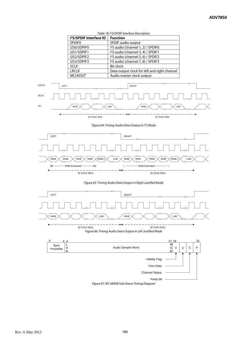
ADV7850
Rev. A May 2012 186
Table 18: I2S/SPDIF Interface Description I2S/SPDIF Interface IO Function SPDIF0 SPDIF audio output I2S0/SDPIF0 I2S audio (channel 1, 2) / SPDIF0 I2S1/SDPIF1 I2S audio (channel 3, 4) / SPDIF1 I2S2/SDPIF2 I2S audio (channel 5, 6) / SPDIF2 I2S3/SDPIF3 I2S audio (channel 7, 8) / SPDIF3 SCLK Bit clock LRCLK Data output clock for left and right channel MCLKOUT Audio master clock output
Figure 64: Timing Audio Data Output in I2S Mode
Figure 65: Timing Audio Data Output in Right Justified Mode
Figure 66: Timing Audio Data Output in Left Justified Mode
Figure 67: IEC 60958 Sub-frame Timing Diagram
LRCLK
SCLK
ISx
LEFT RIGHT
LSBMSB MSB LSB
32 Clock Slots 32 Clock Slots
~ ~~ ~
~ ~~ ~
~ ~~ ~
~ ~~ ~
~ ~~ ~
~ ~
~ ~~ ~
~ ~
LEFT RIGHT
LSBMSB MSB LSB
32 Clock Slots 32 Clock Slots
MSB MSB MSB MSBMSB-1
~ ~~ ~
~ ~~ ~
~ ~~ ~
~ ~~ ~
~ ~~ ~
~ ~~ ~
~ ~~ ~
~ ~~ ~
MSB-1MSB MSB
MSB Extended MSB Extended
LEFT RIGHT
LSBMSB MSB LSB
32 Clock Slots 32 Clock Slots
~ ~~ ~
~ ~~ ~
~ ~~ ~
~ ~
~ ~~ ~
~ ~~ ~
~ ~~ ~
~ ~
Audio Sample WordSync
Preamble V U C PLSB
MSB
0 3 4 27 28 31
Validity Flag
User Data
Channel Status
Parity Bit

ADV7850
Rev. A May 2012 187
Figure 68: AES3 Sub-frame Timing Diagram
Figure 69: AES3 Stream Timing Diagram
7.28.2 DSD Audio Interface and Output Controls The ADV7850 incorporates a 6-DSD channel interface used to output the audio stream extracted from DSD packets. Each of the DSD channels carries an over-sampled 1-bit representation of the audio signal as delivered on Super Audio CDs (SACDs).
Table 19: DSD Interface Description DSD Interface IO Function DSD0A 1st DSD data channel DSD0B 2nd DSD data channel DSD1A 3rd DSD data channel DSD1B 4th DSD data channel DSD2A 5th DSD data channel DSD2B 6th DSD data channel SCLK Bit clock MCLKOUT Audio master clock output
Two controls are provided to change the mapping between the audio output ports and the DSD signals. dsd_map_rot[2:0], Addr 68 (HDMI), Address 0x6D[2:0] This control is used to select the arrangement of the DSD interface on the audio output port pins.
Function dsd_map_rot[2:0] Description 000 [DSD0A on AP0] [DSD0B on AP1] [DSD1A on AP2] [DSD1B on AP3] [DSD2A on AP4] [DSD2B on
AP5] 001 [DSD2B on AP0] [DSD0A on AP1] [DSD0B on AP2] [DSD1A on AP3] [DSD1B on AP4] [DSD2A on
AP5] 010 [DSD2A on AP0] [DSD2B on AP1] [DSD0A on AP2] [DSD0B on A
dsd_map_inv, Addr 68 (HDMI), Address 0x6D[3] This control is used to invert the arrangement of the DSD interface on the audio output port pins. Note the arrangement of the DSD interface on the audio output port pins is determined by dsd_map_rot.
Data V U C BLSB
0 23 24 27
Validity Flag
User Data
Channel Status
Block Start Flag
MSB
0 0 0 0
31
Zero Padding
Channel A Channel B
LSB LSB
32 Clock Slots 32 Clock Slots
MSB MSB V U C BV U C B
Frame n + 1Frame n
~ ~~ ~
~ ~~ ~
~ ~~ ~
~ ~
~ ~~ ~
~ ~~ ~
~ ~~ ~
~ ~

ADV7850
Rev. A May 2012 188
Function dsd_map_inv Description 0 Do not invert arrangement of DSD channels on audio output port pins 1 Invert arrangement of DSD channels on audio output port pins
dsd_map_rot and dsd_map_inv are independent controls. Any combination of values is, therefore, allowed for dsd_map_rot and dsd_map_inv. Table 20 and Table 21 show examples of mappings for the DSD signals.
Table 20: Audio Mapping for dsd_map_rot = 00, dsd_map_inv = 0 (Default) Output Pixel Port Name DSD Interface HA_AP0 DSD0A HA_AP1 DSD0B HA_AP2 DSD1A HA_AP3 DSD1B HA_AP4 DSD2A HA_AP5 DSD2B
Table 21: Audio Mapping for dsd_map_rot = 00, dsd_map_inv = 1 Output Pixel Port Name DSD Interface HA_AP0 DSD2B HA_AP1 DSD2A HA_AP2 DSD1B HA_AP3 DSD1A HA_AP4 DSD0B HA_AP5 DSD0A
Notes: DSD0A and DSD0B output must be used when in stereo mode only. DSD0A and DSD0B always carry the main 2-channel audio data. DSD1A, DSD1B, DSD2A, and DSD2B are the surround channels.
Figure 70: DSD Timing Diagram1
1Where xx is the channel, for example, 0A, 0B By default, the ADV7850 automatically enables the DSD interface if it receives DSD packets. The ADV7850 also automatically enables the I2S interface if it receives audio sample packets or if it does not receive any audio packets. However, it is possible to override the audio interface that is used via the ovr_auto_mux_dsd_out and mux_dsd_out controls. ovr_auto_mux_dsd_out, Addr 68 (HDMI), Address 0x01[3] This control is used to override the DSD/DST output control. In automatic control, DSD or I2S interface is selected according to the type of packet received. The DSD/DST interface is enabled if the part receives DSD or DST audio sample packet. The I2S interface is enabled when the part receives audio sample packets or when no packet is received. In manual mode, mux_dsd_out selects the output interface.
Function ovr_auto_mux_dsd_out Description 0 Automatic DSD/DST output control 1 Override DSD/DST output control
mux_dsd_out, Addr 68 (HDMI), Address 0x01[4] This control is used to set the override for the DSD output.
SCLK
DSDxx
~ ~~ ~
~ ~

ADV7850
Rev. A May 2012 189
Function mux_dsd_out Description 0 Override by outputting I2S data 1 Override by outputting DSD/DST data
7.28.3 DST Audio Interface and Output Controls The ADV7850 incorporates a DST interface that outputs audio data extracted from DST packets. The transfer rate of the DST packets is indicated via dst_double. dst_double, Addr 68 (HDMI), Address 0x19[2] (Read Only) This readback indicates when the DST audio is double data rate.
Function dst_double Description 0 No DST double data rate audio detected 1 DST double data rate audio detected
Important:
• The bit clock frequency equals 64 times the audio sampling frequency, that is, 64 fs • dst_double indicates the transfer rate set by the latest DST packet processed by the ADV7850
A control is provided to change the mapping between the audio output ports and DST signals. dst_map_rot[2:0], Addr 68 (HDMI), Address 0x6E[2:0] This control is used to select the arrangement of the DST interface on the audio output port pins.
Function dst_map_rot[2:0] Description 000 [DST_S on AP0] [DST_FF on AP5] 001 [DST_S on AP1] [DST_FF on AP5] 010 [DST_S on AP2] [DST_FF on AP5] 011 [DST_S on AP3] [DST_FF on AP5] 100 [DST_S on AP4] [DST_FF on AP5] 101 Reserved 110 Reserved 111 Reserved
Table 22: DST Interface Description
DST Interface IO Function DST_S DST stream SCLK Bit clock DST_FF DST frame flag MCLKOUT Audio master clock output
Figure 71: DST Timing Diagram for DST_DOUBLE = 0
Frame n Frame n + 1
DST_CLK
DST_S
DST_FF
~ ~~ ~
~ ~~ ~

ADV7850
Rev. A May 2012 190
Figure 72: DST Timing Diagram for DST_DOUBLE = 1
7.28.4 HBR Interface and Output Controls The ADV7850 can receive HBR audio stream packets. The ADV7850 outputs HBR data over five of the audio output pins in any of the following formats:
• An SDPIF stream conforming to the IEC60958 specification (refer to Figure 67). The following configuration is required to output an SPDIF stream on the HBR output pins: ovr_mux_hbr is set to 0
or ovr_ mux_hbr is set to 1 and mux_hbr_out is set to 1
• A binary stream if one of the following configurations is used: ovr_ mux_hbr is set to 1, mux_hbr_out is set to 0, and i2soutmode[1:0] is set to 0x0 for an I2S mode binary stream
(refer to Figure 64). ovr_ mux_hbr is set to 1, mux_hbr_out is set to 0, and i2soutmode is set to 0x1 for a right justified stream (refer to
Figure 65) ovr_ mux_hbr is set to 1, mux_hbr_out is set to 0, and i2soutmode is set to 0x2 for a left justified stream (refer to
Figure 66) Note: No audio flags are output by the part in these configurations.
• An AES3 stream on each HBR interface output pin (refer to Figure 68 and Figure 69). The following configuration is required to output AES3 streams: ovr_ mux_hbr is set to 1 i2soutmode is set to 0b11
Important:
• Each of the four HBR outputs carry one of four consecutive blocks of the HBR stream • The four streams on the four HBR pin are output at one quarter of the audio sample rate, fs
Table 23: HBR Interface Description
HBR Interface IO Function HA_AP0 1st block of HBR stream (SPDIF format only) HA_AP1 1st block of HBR stream HA_AP2 2nd block of HBR stream HA_AP3 3rd block of HBR stream HA_AP4 4th block of HBR stream SCLK Bit clock LRCLK Data output clock for left and right channel MCLKOUT Audio master clock output
Note: The audio output mapping controls i2s_spdif_map_rot[1:0] and i2s_spdif_map_inv also apply to the HBR output signals. ovr_mux_hbr, Addr 68 (HDMI), Address 0x01[2] This control is used to select automatic or manual configuration for HBR outputs. Automatically, HBR outputs are encoded as SPDIF streams. In manual mode, mux_hbr_out selects the audio output interface.
Frame n Frame n + 1
DST_CLK
DST_S
DST_FF
~ ~~ ~
~ ~~ ~

ADV7850
Rev. A May 2012 191
Function ovr_mux_hbr Description 0 Automatic HBR output control 1 Manual HBR output control
mux_hbr_out, Addr 68 (HDMI), Address 0x01[1] This control is used to manually select the audio output interface for HBR data. It is valid when ovr_mux_hbr is set to 1.
Function mux_hbr_out Description 0 Override by outputting I2S data 1 Override by outputting SPDIF data
7.29 MCLKOUT SETTING The audio master clock MCLKOUT is set using the mclk_fs_n[2:0] register, as shown in Equation 5.
sNMCLKFSMCLKOUT f128)1_( ××+=
Equation 5: Relationship Between MCLKOUT, MCLKFS_N, and fs
mclk_fs_n[2:0], Addr 4C (DPLL), Address 0xB5[2:0] This control is used to select the multiple of 128 fs to be used for MCLK out.
Function mclk_fs_n[2:0] Description 000 128 fs 001 << 256 fs 010 384 fs 011 512 fs 100 640 fs 101 768 fs 110 Not valid 111 Not valid
7.30 AUDIO CHANNEL MODE audio_ch_md_raw indicates if 2-channel audio data or multi-channel audio data is received. audio_ch_md_raw, IO, Address 0x65[4] (Read Only) This readback indicates the raw status signal indicating the layout value of the audio packets that were last received.
Function audio_ch_md_raw Description 0 Last audio packets received have layout value of 1 (e.g. Layout-1 corresponds to 2-channel
audio when audio sample packets are received) 1 Last audio packets received have layout value of 0 (e.g. Layout-0 corresponds to 8-channel
audio when audio sample packets are received) Note: audio_ch_md_raw is valid for audio sample packets and DSD packets.

ADV7850
Rev. A May 2012 192
audio_channel_mode, Addr 68 (HDMI), Address 0x07[6] (Read Only) This readback flags stereo or multichannel audio packets. Note that stereo packets may carry compressed multichannel audio.
Function audio_channel_mode Description 0 Stereo audio (may be compressed multichannel) 1 Multichannel uncompressed audio detected (3-8 channels)
7.31 AUDIO MUTING The ADV7850 integrates an advanced audio mute function that is designed to remove all extraneous noise and pops from a 2-channel L-PCM audio stream at sample frequencies up to 192 kHz. The audio mute controller takes in event detection signals that can be used to determine when an audio mute is needed. The controller generates a mute signal to the audio block and a coast signal to the digital PLL generating the audio clock.
7.31.1 Audio Mute Configuration The ADV7850 can be configured to automatically mute an L-PCM audio stream when selectable mute conditions occur. The audio muting is configured as follows:
• Set the audio muting speed via audio_mute_speed[4:0]. • Set not_auto_unmute as follows:
Set not_auto_unmute to 0 if the audio must be unmuted automatically after a delay set in wait_unmute[2:0] after all selected mute conditions have become inactive.
Set not_auto_unmute to 1 if the audio must be unmuted manually (for example, by an external controller) when all selected mute conditions have become inactive.
Select the mute conditions that trigger an audio mute (refer to Table 24). • Select the Audio PLL coast conditions (refer to Section 7.25.4). • Set wait_unmute[2:0] to configure the audio counter that triggers the audio unmute when it has timed out after all selected mute
conditions have become inactive. The ADV7850 internally unmutes the audio if the following three conditions (listed in order of priority) are met:
• Mute conditions are inactive • not_auto_unmute is set to 0 • Audio unmute counter has finished counting down or is disabled
Notes:
• For the best audio muting performance, set AUDIO_MUTE_SPEED to 1. • Both Table 13 and Table 24 provide a column with the heading ‘Corresponding Status Registers(s)’. This column lists the status
registers that convey information related to their corresponding audio mute masks or coast masks. • The ADV7850 also mutes the DSD stream when one of the selected mute conditions occurs (refer to Table 24) by outputting the
DSD mute pattern 0101010101… A DSD decoder receiving this stream outputs a 0 V mean analog stream. • The ADV7850 never mutes the audio data when it receives an audio sample packet with compressed audio data or HBR packets.
mute_audio, Addr 68 (HDMI), Address 0x1A[4] This control is used to force an internal mute independently of the mute mask conditions.
Function mute_audio Description 0 Audio in normal operation 1 Force audio mute

ADV7850
Rev. A May 2012 193
audio_mute_speed[4:0], Addr 68 (HDMI), Address 0x0F[4:0] This control is used to define the number of samples between each volume change of 1.5 dB when muting and unmuting.
Function audio_mute_speed[4:0] Description xxxxx Number of samples between each volume change of 1.5 dB
not_auto_unmute, Addr 68 (HDMI), Address 0x1A[0] This control is used to disable the auto unmute feature. When set to 1, audio can be unmuted manually if all mute conditions are inactive by setting not_auto_unmute to 0 and then back to 1.
Function not_auto_unmute Description 0 Audio unmutes following a delay set by wait_unmute after all mute conditions become
inactive 1 Prevents audio from unmuting automatically
wait_unmute[2:0], Addr 68 (HDMI), Address 0x1A[3:1] This control is used to delay audio unmute. Once all mute conditions are inactive, wait_unmute[2:0] can specify a further delay time before unmuting. not_auto_unmute must be set to 0 for this control to be effective.
Function wait_unmute[2:0] Description 000 Disable/cancel delayed unmute; audio unmutes directly after all mute conditions become
inactive 001 Unmute 250 ms after all mute conditions become inactive 010 Unmute 500 ms after all mute conditions become inactive 011 Unmute 750 ms after al
Table 24: Selectable Mute Conditions
Bit Name HDMI Map Address
Description Corresponding Status Registers(s)
mt_msk_comprs_aud 0x14[5]
Causes audio mute if audio is compressed cs_data[1]
mt_msk_aud_mode_chng 0x14[4] Causes audio mute if audio mode changes between PCM, DST DSD, or HBR formats
audio_sample_pckt_det
mt_msk_parity_err 0x14[1] Causes audio mute if parity bits in audio samples are not correct
parity_error_raw
mt_msk_vclk_chng 0x14[0] Causes audio mute if TMDS clock has irregular/missing pulses
vclk_chng_raw
mt_msk_apll_unlock 0x15[7] Causes audio mute if audio PLL unlocks audio_pll_locked mt_msk_vpll_unlock 0x15[6] Causes audio mute if TMDS PLL unlocks tmds_pll_locked mt_msk_acr_not_det 0x15[5] Causes audio mute if ACR packets are not received within
one VSync audio_c_pckt_raw
mt_msk_flatline_det 0x15[3] Causes audio mute if flatline bit in audio packets is set audio_flt_line_raw mt_msk_fifo_underflow 0x15[1] Causes audio mute if audio FIFO underflows fifo_underflo_raw mt_msk_fifo_overflow 0x15[0] Causes audio mute if audio FIFO overflows fifo_overflo_raw mt_msk_avmute 0x16[7] Causes audio mute if AVMute is set in the general control
packet av_mute_raw
mt_msk_not_hdmimode 0x16[6] Causes audio mute if HDMI_MODE bit goes low hdmi_mode mt_msk_new_cts 0x16[5] Causes audio mute if CTS changes by more than the
threshold set in cts_change_threshold[5:0] cts_pass_thrsh_raw
mt_msk_new_n 0x16[4] Causes audio mute if N changes change_n_raw mt_msk_chmode_chng 0x16[3] Causes audio mute if the channel mode changes from
stereo to multichannel, or vice versa audio_mode_chng_raw
mt_msk_apckt_ecc_err 0x16[2] Causes audio mute if uncorrectable error is detected in the audio_pckt_err_raw

ADV7850
Rev. A May 2012 194
Bit Name HDMI Map Address
Description Corresponding Status Registers(s)
audio packets by the ECC block mt_msk_chng_port 0x16[1] Causes audio mute if HDMI port is changed hdmi_port_select[2:0] mt_msk_vclk_det 0x16[0] Causes audio mute if TMDS clock is not detected tmds_clk_a_raw
tmds_clk_b_raw tmds_clk_c_raw tmds_clk_d_raw
7.31.2 Internal Mute Status The internal mute status is provided through the internal_mute_raw control. internal_mute_raw, IO, Address 0x65[6] (Read Only) This readback indicates the raw status signal of the internal mute signal.
Function internal_mute_raw Description 0 Audio not muted 1 Audio muted
7.31.3 AV Mute Status av_mute, Addr 68 (HDMI), Address 0x04[6] (Read Only) This readback displays the avmute status received in the last general control packet received.
Function av_mute Description 0 avmute not set 1 avmute set
7.31.4 Audio Stream with Incorrect Parity Error The ADV7850 discards audio sample packets that have an incorrect parity bit. When these samples are received, the ADV7850 repeats the previous audio sample with a valid parity bit. The audio stream out of the ADV7850 can be muted in this situation if the audio mute mask mt_msk_parity_err is set. It is possible to configure the ADV7850 so that it processes audio sample packets that have an incorrect parity bit and corrects the parity bit. The ADV7850 can then output an audio stream even when the parity bits from the audio sample packet are invalid. This configuration is activated by setting mt_msk_parity_err to 0 and ignore_parity_err to 1. ignore_parity_err, Addr 68 (HDMI), Address 0x1A[6] This control is used to select the processing of audio samples even when they have a parity error.
Function ignore_parity_err Description 0 Discard audio sample packets that have invalid parity bit 1 Process audio sample packets that have invalid parity bit
mt_msk_parity_err, Addr 68 (HDMI), Address 0x14[1] This control is used to set the audio mute mask for a parity error. It sets the audio mutes if an audio sample packet is received with an incorrect parity bit.

ADV7850
Rev. A May 2012 195
Function mt_msk_parity_err Description 1 Audio mute occurs if audio sample packet is received with incorrect parity bit.
7.32 AUDIO CLOCK REGENERATION PARAMETERS The ADV7850 recreates an internal audio master clock using Audio Clock Regeneration (ACR) values transmitted by the HDMI source.
7.32.1 ACR Parameters Readbacks The registers N and CTS can be read back from the HDMI Map. cts[19:0], Addr 68 (HDMI), Address 0x5B[7:0]; Address 0x5C[7:0]; Address 0x5D[7:4] (Read Only) This readback indicates the CTS value received in the HDMI datastream.
Function cts[19:0] Description 00000000000000000000
Default CTS value readback from HDMI stream
xxxxxxxxxxxxxxxxxxxx CTS value readback from HDMI stream n[19:0], Addr 68 (HDMI), Address 0x5D[3:0]; Address 0x5E[7:0]; Address 0x5F[7:0] (Read Only) This readback indicates the N value received in the HDMI datastream.
Function n[19:0] Description 00000000000000000000
Default N value readback from HDMI stream
xxxxxxxxxxxxxxxxxxxx N value readback from HDMI stream Note: A buffer has been implemented for the N and CTS readback registers. A read of the HDMI Map, Address 0x5B register updates the buffer that stores the N and CTS readback registers. The buffer implemented for N and CTS readback allows the reading of both N and CTS registers within an I2C block read.
7.32.2 Monitoring ACR Parameters The reception of ACR packets can be notified via audio_c_pckt_raw. Changes in N and CTS can be monitored via change_n_raw and cts_pass_thrsh_raw, as described in this section. audio_c_pckt_raw, IO, Address 0x65[1] (Read Only) This readback indicates the raw status signal of the audio clock regeneration packet detection signal.
Function audio_c_pckt_raw Description 0 No audio clock regeneration packets received since last HDMI reset condition 1 Audio clock regeneration packets received
change_n_raw, IO, Address 0x7E[3] (Read Only) This readback indicates the status of the ACR N value changed interrupt signal. Once set to 1, it indicates the N value of the ACR packets has changed. Once set, this bit remains high until it is cleared via change_n_clr.

ADV7850
Rev. A May 2012 196
Function change_n_raw Description 0 Audio clock regeneration N value not changed 1 Audio clock regeneration N value changed
cts_pass_thrsh_raw, IO, Address 0x7E[4] (Read Only) This readback indicates the status of the ACR CTS value exceed threshold interrupt signal. When set to 1, it indicates the CTS value of the ACR packets has exceeded the threshold set by cts_change_threshold. Once set, this bit remains high until it is cleared.
Function cts_pass_thrsh_raw Description 0 Audio clock regeneration CTS value not passed threshold 1 Audio clock regeneration CTS value changed more than threshold
cts_change_threshold[5:0], Addr 68 (HDMI), Address 0x10[5:0] This control is used to set the tolerance for change in the CTS value. This tolerance is used for the audio mute mask, mt_msk_new_cts; the HDMI status bit, cts_pass_thrsh_raw; and the HDMI interrupt status bit, cts_pass_thrsh_st. It controls the amounts of LSBs that the CTS can change before an audio mute, status change or interrupt is triggered.
Function cts_change_threshold[5:0]
Description
100101 Default tolerance of CTS value for cts_pass_thrsh_raw and mt_msk_new_cts xxxxxx Tolerance of CTS value for cts_pass_thrsh_raw and mt_msk_new_cts
7.33 CHANNEL STATUS Channel status bits are extracted from the HDMI audio packets of the 1st audio channel (that is, channel 0) and stored in registers channel_status_data_x of the HDMI Map (where x is 1, 2, 3, 4 and 5).
7.33.1 Validity Status Flag The channel status readback described in Section 7.33 should be considered valid if cs_data_valid_raw is set to 1. Figure 73 shows the algorithm that can be implemented to monitor the read valid channel status bit using cs_data_valid_raw. cs_data_valid_raw, IO, Address 0x65[7] (Read Only) This readback indicates the raw status signal of the channel status data valid signal.
Function cs_data_valid_raw Description 0 Channel status data not valid 1 Channel status data valid

ADV7850
Rev. A May 2012 197
Figure 73: Reading Valid Channel Status Flags
Notes:
• cs_data_valid_raw indicates that the first 40 of the channel status bits sent by the upstream transmitter have been correctly collected. This bit does not indicate if the content of the channel status bit is corrupted as this is indeterminable.
• A corresponding interrupt can be enabled for cs_data_valid_raw by setting the mask cs_data_valid_mb1 or cs_data_valid_mb2. Refer to Section 15 for additional information on the interrupt feature.
7.33.2 General Control and Mode Information The general control and mode information are specified in Byte 0 of the channel status. For more information, refer to the IEC60958 standards. cs_data[0], Consumer/Professional Application, HDMI Map, Address 0x36, [0]
Function cs_data[0] Description 0 << Consumer application 1 Professional application
cs_data[1], PCM/non-PCM Audio Sample, HDMI Map, Address 0x36, [1]
Function cs_data[1] Description 0 << Audio sample word represents linear PCM samples 1 Audio sample word used for other purposes
Start
Is CS_DATA_VALID_S
T set to 1 ?
YES
Enable the CS_DATA_VALID_ST interrupt
Is CS_DATA_VALID_R
AW set to 1
NO
Is CS_DATA_VALID_S
T set to 1 ?
YES
YES
Set CS_DATA_VALID_CLR to 1
NO
Read the channel status bits in HDMI Map Reg 0x36 to 0x3A
The channel status bits previously read are not valid
The channel status bits previously read are valid
NO
Initialization
Check if the CS_DATA_VALID interrupt has triggered
Read the channel status bitsand decide if they are valid

ADV7850
Rev. A May 2012 198
cs_data[2], Copyright, HDMI Map, Address 0x36, [2]
Function cs_data[2] Description 0 << Software for which copyright is asserted 1 Software for which no copyright is asserted
cs_data[5:3], Emphasis, HDMI Map, Address 0x36, [5:3]
Function cs_data[5:3]1 Description 000 << Two audio channels without pre-emphasis 001 Two audio channels with 50/15 pre-emphasis
1 Unspecified values are reserved cs_data[7:6], Channel Status Mode, HDMI Map, Address 0x36, [7:6]
Function cs_data[7:6]1 Description 00 << Mode 0
1Unspecified values are reserved
7.33.3 Category Code The category code is specified in Byte 1 of the channel status. The category code indicates the type of equipment that generates the digital audio interface signal. For more information, refer to the IEC60958 standards. cs_data[15:8], Category Code, HDMI Map, Address 0x37, [7:0]
Function cs_data[15:8] Description xxxx xxxx Category code1 0000 0000 << Reset value
1Refer to IEC60958-3 standards
7.33.4 Source Number and Channel Number cs_data[19:16], Source Number, HDMI Map, Address 0x38, [3:0]
Function cs_data[19:16] Description xxxx Source number1 0000 << Reset value
1Refer to IEC60958-3 standards cs_data[23:20], Channel Number, HDMI Map, Address 0x38, [7:4]
Function cs_data[23:20] Description xxxxx Channel number1 00000 << Reset value
1Refer to IEC60958-3 standards
7.33.5 Sampling and Frequency Accuracy The sampling frequency and clock accuracy are specified by Byte 3 of the channel status. For additional information, refer to the IEC60958 standards.

ADV7850
Rev. A May 2012 199
cs_data[27:24], Sampling Frequency, HDMI Map, Address 0x39, [3:0]
Function cs_data[27:24]1 Description 0000 << 44.1 kHz 0010 48 kHz 0011 32 kHz 1000 88.2 kHz 1010 96 kHz 1100 176 kHz 1110 192 kHz
1 Unspecified values are reserved cs_data[29:28], Clock Accuracy, HDMI Map, Address 0x39, [5:4]
Function cs_data[29:28] Description 00 << Level II, ±1000 ppm 01 Level I, ±50 ppm 10 Level III, variable pitch shifted 11 Reserved
cs_data[31:30], Reserved Register, HDMI Map, Address 0x39, [7:6]
Function cs_data[31:30] Description XX Reserved 00 << Reset value
7.33.6 Word Length Word length information is specified in Byte 4 of the channel status bit. For more information, refer to the IEC60958 standards. cs_data[32], Maximum Word Length Size, HDMI Map, Address 0x3A, [0]
Function cs_data[32] Description 0 << Maximum audio sample word length is 20 bits 1 Maximum audio sample word length is 24 bits
cs_data[35:33], Word Length, HDMI Map, Address 0x3A, [3:1]
Function cs_data[35:33]1 Description Audio sample word length if maximum
length is 24 as indicated by cs_data[32] Audio sample word length if maximum length is 20 as indicated by cs_data[32]
000 << Word length not indicated Word length not indicated 001 20 bits 16 bits 010 22 bits 18 bits 100 23 bits 19 bits 101 24 bits 20 bits 110 21 bits 21bits
1Unspecified values are reserved
7.33.7 Channel Status Copyright Value Assertion It is possible to overwrite the copyright value of the channel status bit that is passed to the SPDIF output. This is done via the
ADV7850
Rev. A May 2012 200
cs_copyright_manual and cs_copyright_value controls. cs_copyright_manual, Addr 68 (HDMI), Address 0x50[1] This control is used to select an automatic or manual setting of the copyright value of the channel status bit that is passed to the SPDIF output. Manual control is set with the cs_copyright_value bit.
Function cs_copyright_manual Description 0 Automatic CS copyright control 1 Manual CS copyright control
cs_copyright_value, Addr 68 (HDMI), Address 0x50[0] This control is used to set the CS copyright value when in manual configuration of the CS copyright bit that is passed to the SPDIF output.
Function cs_copyright_value Description 0 Copyright value of channel status bit is 0. Valid only if cs_copyright_manual is set to 1. 1 Copyright value of channel status bit is 1. Valid only if cs_copyright_manual is set to 1.
7.33.8 Monitoring Change of Audio Sampling Frequency
The ADV7850 features the new_samp_rt_raw control to monitor changes in the audio sampling frequency field of the channel status bits. new_samp_rt_raw, IO, Address 0x83[3] (Read Only) This readback indicates the status of the new sampling rate interrupt signal. When set to 1, it indicates that the audio sampling frequency field in the channel status data has changed. Once set, this bit remains high until it is cleared via new_samp_rt_clr.
Function new_samp_rt_raw Description 0 Sampling rate bits of the channel status data on audio channel 0 not changed 1 Sampling rate bits of the channel status data on audio channel 0 changed
Important: new_samp_rt_raw does not trigger if cs_data_valid_raw is set to 0. This prevents the notification of a change from a valid to an invalid audio sampling frequency readback in the channel status bits, and vice versa.
7.34 PACKETS AND INFOFRAMES REGISTERS In HDMI, auxiliary data is carried across the digital link using a series of packets. The ADV7850 automatically detects and stores the following HDMI packets:
• InfoFrames • Audio Content Protection (ACP) • International Standard Recording Code (ISRC) • Gamut Metadata
When the ADV7850 receives one of these packets, it computes the packet checksum and compares it with the checksum available in the packet. If these checksums are the same, the packets are stored in the corresponding registers. If the checksums are not the same, the packets are discarded. Refer to the EIA/CEA-861D specifications for more information on the packets fields.

ADV7850
Rev. A May 2012 201
7.34.1 InfoFrames Registers The ADV7850 can store the following InfoFrames:
• Auxiliary Video Information (AVI) InfoFrame • Source Production Descriptor (SPD) InfoFrame • Audio InfoFrame • Moving Picture Expert Group (MPEG) Source InfoFrame
7.34.2 InfoFrame Collection Mode The ADV7850 has two modes for storing the InfoFrame packet sent from the source into the internal memory. By default, the ADV7850 only stores the InfoFrame packets received if the checksum is correct for each InfoFrame. The ADV7850 also provides a mode to store every InfoFrame sent from the source, regardless of an InfoFrame packet checksum error. always_store_inf, Addr 68 (HDMI), Address 0x47[0] This control is used to force InfoFrames with checksum errors to be stored.
Function always_store_inf Description 0 Store data from received InfoFrames only if their checksum correct 1 Always store data from received InfoFrame regardless of their checksum
7.34.3 InfoFrame Checksum Error Flags The following checksum error status registers flag when the last InfoFrame received has a checksum error. Once set, these bits remain high until the interrupt is cleared via their corresponding clear bits. avi_inf_cks_err_raw, IO, Address 0x88[4] (Read Only) This readback displays the status of the AVI InfoFrame checksum error interrupt signal. When set to 1, it indicates that a checksum error was detected for an AVI InfoFrame. Once set, this bit remains high until it is cleared via avi_inf_cks_err_clr.
Function avi_inf_cks_err_raw Description 0 No AVI InfoFrame checksum error occurred 1 An AVI InfoFrame checksum error occurred
aud_inf_cks_err_raw, IO, Address 0x88[5] (Read Only) This readback displays the status of the audio InfoFrame checksum error interrupt signal. When set to 1, it indicates that a checksum error was detected for an audio InfoFrame. Once set, this bit remains high until it is cleared via audio_inf_cks_err_clr.
Function aud_inf_cks_err_raw Description 0 No audio InfoFrame checksum error occurred 1 Audio InfoFrame checksum error occurred
spd_inf_cks_err_raw, IO, Address 0x88[6] (Read Only) This readback displays the status of the SPD InfoFrame checksum error interrupt signal. When set to 1, it indicates that a checksum error was detected for an SPD InfoFrame. Once set, this bit remains high until it is cleared via spd_inf_cks_err_clr.

ADV7850
Rev. A May 2012 202
Function spd_inf_cks_err_raw Description 0 No SPD InfoFrame checksum error occurred 1 SPD InfoFrame checksum error occurred
ms_inf_cks_err_raw, IO, Address 0x88[7] (Read Only) This readback indicates the status of the MPEG source InfoFrame checksum error interrupt signal. When set to 1, it indicates that a checksum error was detected for an MPEG source InfoFrame. Once set, this bit remains high until it is cleared via ms_inf_ck_clr.
Function ms_inf_cks_err_raw Description 0 No MPEG source InfoFrame checksum error occurred 1 MPEG source InfoFrame checksum error occurred
vs_inf_cks_err_raw, IO, Address 0x8D[0] (Read Only) This readback indicates the status of the vendor specific InfoFrame checksum error interrupt signal. When set to 1, it indicates that a checksum error was detected for a vendor specific InfoFrame. Once set, this bit remains high until it is cleared.
Function vs_inf_cks_err_raw Description 0 No vendor specific InfoFrame checksum error occurred 1 Vendor specific InfoFrame checksum error occurred
7.34.4 AVI InfoFrame Registers Table 25 provides a list of readback registers for the AVI InfoFrame data. Refer to the EIA/CEA-861D specifications for a detailed explanation of the AVI InfoFrame fields.
Table 25: AVI InfoFrame Registers InfoFrame Map Address
Access Type Register Name Byte Name1
0xE0 R/W avi_packet_id[7:0] Packet Type Value 0xE1 R avi_inf_ver InfoFrame version number 0xE2 R avi_inf_len InfoFrame length 0x00 R avi_inf_pb_0_1 Checksum 0x01 R avi_inf_pb_0_2 Data Byte 1 0x02 R avi_inf_pb_0_3 Data Byte 2 0x03 R avi_inf_pb_0_4 Data Byte 3 0x04 R avi_inf_pb_0_5 Data Byte 4 0x05 R avi_inf_pb_0_6 Data Byte 5 0x06 R avi_inf_pb_0_7 Data Byte 6 0x07 R avi_inf_pb_0_8 Data Byte 7 0x08 R avi_inf_pb_0_9 Data Byte 8 0x09 R avi_inf_pb_0_10 Data Byte 9 0x0A R avi_inf_pb_0_11 Data Byte 10 0x0B R avi_inf_pb_0_12 Data Byte 11 0x0C R avi_inf_pb_0_13 Data Byte 12 0x0D R avi_inf_pb_0_14 Data Byte 13 0x0E R avi_inf_pb_0_15 Data Byte 14 0x0F R avi_inf_pb_0_16 Data Byte 15 0x10 R avi_inf_pb_0_17 Data Byte 16 0x11 R avi_inf_pb_0_18 Data Byte 17 0x12 R avi_inf_pb_0_19 Data Byte 18
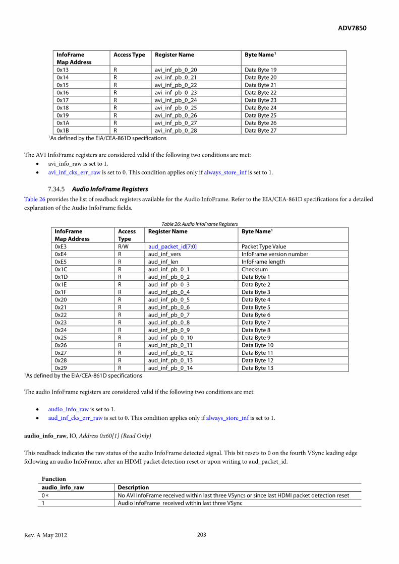
ADV7850
Rev. A May 2012 203
InfoFrame Map Address
Access Type Register Name Byte Name1
0x13 R avi_inf_pb_0_20 Data Byte 19 0x14 R avi_inf_pb_0_21 Data Byte 20 0x15 R avi_inf_pb_0_22 Data Byte 21 0x16 R avi_inf_pb_0_23 Data Byte 22 0x17 R avi_inf_pb_0_24 Data Byte 23 0x18 R avi_inf_pb_0_25 Data Byte 24 0x19 R avi_inf_pb_0_26 Data Byte 25 0x1A R avi_inf_pb_0_27 Data Byte 26 0x1B R avi_inf_pb_0_28 Data Byte 27
1As defined by the EIA/CEA-861D specifications
The AVI InfoFrame registers are considered valid if the following two conditions are met: • avi_info_raw is set to 1. • avi_inf_cks_err_raw is set to 0. This condition applies only if always_store_inf is set to 1.
7.34.5 Audio InfoFrame Registers Table 26 provides the list of readback registers available for the Audio InfoFrame. Refer to the EIA/CEA-861D specifications for a detailed explanation of the Audio InfoFrame fields.
Table 26: Audio InfoFrame Registers InfoFrame Map Address
Access Type
Register Name Byte Name1
0xE3 R/W aud_packet_id[7:0] Packet Type Value 0xE4 R aud_inf_vers InfoFrame version number 0xE5 R aud_inf_len InfoFrame length 0x1C R aud_inf_pb_0_1 Checksum 0x1D R aud_inf_pb_0_2 Data Byte 1 0x1E R aud_inf_pb_0_3 Data Byte 2 0x1F R aud_inf_pb_0_4 Data Byte 3 0x20 R aud_inf_pb_0_5 Data Byte 4 0x21 R aud_inf_pb_0_6 Data Byte 5 0x22 R aud_inf_pb_0_7 Data Byte 6 0x23 R aud_inf_pb_0_8 Data Byte 7 0x24 R aud_inf_pb_0_9 Data Byte 8 0x25 R aud_inf_pb_0_10 Data Byte 9 0x26 R aud_inf_pb_0_11 Data Byte 10 0x27 R aud_inf_pb_0_12 Data Byte 11 0x28 R aud_inf_pb_0_13 Data Byte 12 0x29 R aud_inf_pb_0_14 Data Byte 13
1As defined by the EIA/CEA-861D specifications The audio InfoFrame registers are considered valid if the following two conditions are met:
• audio_info_raw is set to 1. • aud_inf_cks_err_raw is set to 0. This condition applies only if always_store_inf is set to 1.
audio_info_raw, IO, Address 0x60[1] (Read Only) This readback indicates the raw status of the audio InfoFrame detected signal. This bit resets to 0 on the fourth VSync leading edge following an audio InfoFrame, after an HDMI packet detection reset or upon writing to aud_packet_id.
Function audio_info_raw Description 0 No AVI InfoFrame received within last three VSyncs or since last HDMI packet detection reset 1 Audio InfoFrame received within last three VSync
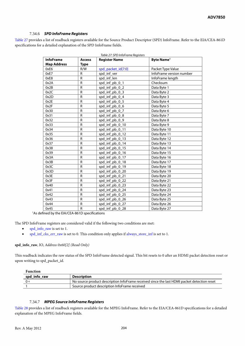
ADV7850
Rev. A May 2012 204
7.34.6 SPD InfoFrame Registers Table 27 provides a list of readback registers available for the Source Product Descriptor (SPD) InfoFrame. Refer to the EIA/CEA-861D specifications for a detailed explanation of the SPD InfoFrame fields.
Table 27: SPD InfoFrame Registers InfoFrame Map Address
Access Type
Register Name Byte Name1
0xE6 R/W spd_packet_id[7:0] Packet Type Value 0xE7 R spd_inf_ver InfoFrame version number 0xE8 R spd_inf_len InfoFrame length 0x2A R spd_inf_pb_0_1 Checksum 0x2B R spd_inf_pb_0_2 Data Byte 1 0x2C R spd_inf_pb_0_3 Data Byte 2 0x2D R spd_inf_pb_0_4 Data Byte 3 0x2E R spd_inf_pb_0_5 Data Byte 4 0x2F R spd_inf_pb_0_6 Data Byte 5 0x30 R spd_inf_pb_0_7 Data Byte 6 0x31 R spd_inf_pb_0_8 Data Byte 7 0x32 R spd_inf_pb_0_9 Data Byte 8 0x33 R spd_inf_pb_0_10 Data Byte 9 0x34 R spd_inf_pb_0_11 Data Byte 10 0x35 R spd_inf_pb_0_12 Data Byte 11 0x36 R spd_inf_pb_0_13 Data Byte 12 0x37 R spd_inf_pb_0_14 Data Byte 13 0x38 R spd_inf_pb_0_15 Data Byte 14 0x39 R spd_inf_pb_0_16 Data Byte 15 0x3A R spd_inf_pb_0_17 Data Byte 16 0x3B R spd_inf_pb_0_18 Data Byte 17 0x3C R spd_inf_pb_0_19 Data Byte 18 0x3D R spd_inf_pb_0_20 Data Byte 19 0x3E R spd_inf_pb_0_21 Data Byte 20 0x3F R spd_inf_pb_0_22 Data Byte 21 0x40 R spd_inf_pb_0_23 Data Byte 22 0x41 R spd_inf_pb_0_24 Data Byte 23 0x42 R spd_inf_pb_0_25 Data Byte 24 0x43 R spd_inf_pb_0_26 Data Byte 25 0x44 R spd_inf_pb_0_27 Data Byte 26 0x45 R spd_inf_pb_0_28 Data Byte 27
1As defined by the EIA/CEA-861D specifications The SPD InfoFrame registers are considered valid if the following two conditions are met:
• spd_info_raw is set to 1. • spd_inf_cks_err_raw is set to 0. This condition only applies if always_store_inf is set to 1.
spd_info_raw, IO, Address 0x60[2] (Read Only) This readback indicates the raw status of the SPD InfoFrame detected signal. This bit resets to 0 after an HDMI packet detection reset or upon writing to spd_packet_id.
Function spd_info_raw Description 0 No source product description InfoFrame received since the last HDMI packet detection reset 1 Source product description InfoFrame received
7.34.7 MPEG Source InfoFrame Registers Table 28 provides a list of readback registers available for the MPEG InfoFrame. Refer to the EIA/CEA-861D specifications for a detailed explanation of the MPEG InfoFrame fields.

ADV7850
Rev. A May 2012 205
Table 28: MPEG InfoFrame Registers
InfoFrame Map Address
Access Type
Register Name Byte Name1
0xE9 R/W ms_packet_id[7:0] Packet Type Value 0xEA R ms_inf_vers InfoFrame version number 0xEB R ms_inf_len InfoFrame length 0x46 R ms_inf_pb_0_1 Checksum 0x47 R ms_inf_pb_0_2 Data Byte 1 0x48 R ms_inf_pb_0_3 Data Byte 2 0x49 R ms_inf_pb_0_4 Data Byte 3 0x4A R ms_inf_pb_0_5 Data Byte 4 0x4B R ms_inf_pb_0_6 Data Byte 5 0x4C R ms_inf_pb_0_7 Data Byte 6 0x4D R ms_inf_pb_0_8 Data Byte 7 0x4E R ms_inf_pb_0_9 Data Byte 8 0x4F R ms_inf_pb_0_10 Data Byte 9 0x50 R ms_inf_pb_0_11 Data Byte 10 0x51 R ms_inf_pb_0_12 Data Byte 11 0x52 R ms_inf_pb_0_13 Data Byte 12 0x53 R ms_inf_pb_0_14 Data Byte 13
1As defined by the EIA/CEA-861D specifications The MPEG InfoFrame registers are considered valid if the following two conditions are met:
• ms_info_raw is set to 1. • ms_inf_cks_err_raw is set to 0. This condition applies only if always_store_inf is set to 1.
ms_info_raw, IO, Address 0x60[3] (Read Only) This readback indicates the raw status signal of the MPEG source InfoFrame detection signal. This bit resets to 0 after an HDMI packet detection reset or upon writing to ms_packet_id.
Function ms_info_raw Description 0 No MPEG InfoFrame received within last three VSyncs or since last HDMI packet detection
reset 1 MPEG source InfoFrame received
7.34.8 Vendor Specific InfoFrame Registers Table 29 provides a list of readback registers available for the Vendor Specific InfoFrame.
Table 29: VS InfoFrame Registers
InfoFrame Map Address
R/W Register Name Byte Name
0xEC R vs_packet_id[7:0] Packet Type Value 0xED R vs_inf_vers InfoFrame version number 0xEE R vs_inf_len InfoFrame length 0x54 R vs_inf_pb_0_1 Checksum 0x55 R vs_inf_pb_0_2 Data Byte 1 0x56 R vs_inf_pb_0_3 Data Byte 2 0x57 R vs_inf_pb_0_4 Data Byte 3 0x58 R vs_inf_pb_0_5 Data Byte 4 0x59 R vs_inf_pb_0_6 Data Byte 5 0x5A R vs_inf_pb_0_7 Data Byte 6 0x5B R vs_inf_pb_0_8 Data Byte 7 0x5C R vs_inf_pb_0_9 Data Byte 8 0x5D R vs_inf_pb_0_10 Data Byte 9 0x5E R vs_inf_pb_0_11 Data Byte 10

ADV7850
Rev. A May 2012 206
InfoFrame Map Address
R/W Register Name Byte Name
0x5F R vs_inf_pb_0_12 Data Byte 11 0x60 R vs_inf_pb_0_13 Data Byte 12 0x61 R vs_inf_pb_0_14 Data Byte 13 0x62 R vs_inf_pb_0_15 Data Byte 14 0x63 R vs_inf_pb_0_16 Data Byte 15 0x64 R vs_inf_pb_0_17 Data Byte 16 0x65 R vs_inf_pb_0_18 Data Byte 17 0x66 R vs_inf_pb_0_19 Data Byte 18 0x67 R vs_inf_pb_0_20 Data Byte 19 0x68 R vs_inf_pb_0_21 Data Byte 20 0x69 R vs_inf_pb_0_22 Data Byte 21 0x6A R vs_inf_pb_0_23 Data Byte 22 0x6B R vs_inf_pb_0_24 Data Byte 23 0x6C R vs_inf_pb_0_25 Data Byte 24 0x6D R vs_inf_pb_0_26 Data Byte 25 0x6E R vs_inf_pb_0_27 Data Byte 26 0x6F R vs_inf_pb_0_28 Data Byte 27
The Vendor Specific InfoFrame registers are considered valid if the following two conditions are met:
• vs_info_raw is set to 1. • vs_inf_cks_err_raw is set to 0. This condition applies only if always_store_inf is set to 1.
vs_info_raw, IO, Address 0x60[4] (Read Only) This readback indicates the raw status signal of the vendor specific InfoFrame detection signal. This bit resets to 0 after HDMI packet detection reset or upon writing to vs_packet_id.
Function vs_info_raw Description 0 No new vendor specific InfoFrame received since last HDMI packet detection reset 1 New vendor specific InfoFrame received
7.34.9 Multiple InfoFrames Support ( THX Media Director™) The ADV7850 supports the reception of multiple InfoFrame packets in a single frame and allows the user to read any of the packets. For example, the HDMI specification defines only one Vendor Specific InfoFrame (VSI) per frame. For support of some inputs which use THX Media Director, it is required to be able to receive three VSIs at the same time. The ADV7850 can detect the number of incoming VSIs and select which VSI to decode, load it into the buffer, read it in the system, and then select another VSI to be decoded and loaded into the buffer. The ADV7850 can select up to 16 different VSIs to be decoded and loaded into the buffer. The default configuration in the ADV7850 is to use VSIs, however this feature can be used for any of the InfoFrame packets described in Section 7.34.1 to Section 7.34.8. The ADV7850 detects how many packets of a configurable type (e.g. VSI) come in between VSync rising edges, and the user can select with an I2C control which of those count-wise they want to pick up in the single VSI data buffer for I2C readback. This way the system can sweep through all the VSI in sequence after it is done reading one of the VSI from the single/shared data buffer. en_pkt_cnt_sel, Addr 7C (InfoFrame), Address 0xFE[4] This control enables the feature where the user can choose which of the multiple received packets per frame of type PKT_CNT_ID is to be collected. This feature is only relevant for packet types that can be stored in the InfoFrame Map.

ADV7850
Rev. A May 2012 207
Function en_pkt_cnt_sel Description 0 Disabled, collect every packet as it is received 1 Enable selectively collecting one of multiple packets per frame of the same type
pkt_cnt_sel[3:0], Addr 7C (InfoFrame), Address 0xFE[3:0] This control selects which one of the multiple received packets per frame of type pkt_cnt_id is to be collected. It must be enabled with en_pkt_cnt_sel. It should be manually changed after receiving the corresponding new packet detect flag.
Function pkt_cnt_sel[3:0] Description 0000 Select 1st packet after VSync rising edge xxxx 1110 Select 15th packet after VSync rising edge 1111 Undefined
rb_pkt_cnt[3:0], Addr 7C (InfoFrame), Address 0xFF[3:0] (Read Only) This readback displays the count of number of packets of type pkt_cnt_id per frame, as detected between VSync rising edges. The count readback is supported for any pkt_cnt_id, even those packets that cannot be stored in the InfoFrame Map, e.g. general control packets. pkt_cnt_id[7:0], Addr 7C (InfoFrame), Address 0xFD[7:0] This control is used to select which type of packet is going to be counted during each frame. Any packet header ID is supported to detect the count, but only collectable packets can be stored. The default is 0x81 for vendor specific InfoFrame.
Function pkt_cnt_id[7:0] Description 10000001 default
7.35 PACKET REGISTERS
7.35.1 ACP Packet Registers Table 30 provides the list of readback registers available for the ACP packets. Refer to the HDMI 1.4 specifications for a detailed explanation of the ACP packet fields.
Table 30: ACP Packet Registers InfoFrame Map Address
R/W Register Name Packet Byte No.1
0xEF R/W acp_packet_id[7:0] Packet Type Value 0xF0 R acp_type HB1 0xF1 R acp_header2 HB2 0x70 R acp_pb_0_1 PB0 0x71 R acp_pb_0_2 PB1 0x72 R acp_pb_0_3 PB2 0x73 R acp_pb_0_4 PB3 0x74 R acp_pb_0_5 PB4 0x75 R acp_pb_0_6 PB5 0x76 R acp_pb_0_7 PB6 0x77 R acp_pb_0_8 PB7 0x78 R acp_pb_0_9 PB8 0x79 R acp_pb_0_10 PB9 0x7A R acp_pb_0_11 PB10 0x7B R acp_pb_0_12 PB11 0x7C R acp_pb_0_13 PB12

ADV7850
Rev. A May 2012 208
InfoFrame Map Address
R/W Register Name Packet Byte No.1
0x7D R acp_pb_0_14 PB13 0x7E R acp_pb_0_15 PB14 0x7F R acp_pb_0_16 PB15 0x80 R acp_pb_0_17 PB16 0x81 R acp_pb_0_18 PB17 0x82 R acp_pb_0_19 PB18 0x83 R acp_pb_0_20 PB19 0x84 R acp_pb_0_21 PB20 0x85 R acp_pb_0_22 PB21 0x86 R acp_pb_0_23 PB22 0x87 R acp_pb_0_24 PB23 0x88 R acp_pb_0_25 PB24 0x89 R acp_pb_0_26 PB25 0x8A R acp_pb_0_27 PB26 0x8B R acp_pb_0_28 PB27
1As defined by the HDMI 1.4 specifications The ACP InfoFrame registers are considered valid if acp_pckt_raw is set to 1. acp_pckt_raw, IO, Address 0x60[5] (Read Only) This readback indicates the raw status signal of the audio content protection packet detection signal. This bit resets to 0 after an HDMI packet detection reset or upon writing to acp_packet_id.
Function acp_pckt_raw Description 0 No ACP packet received within last 600 ms or since last HDMI packet detection reset 1 ACP packets received within last 600 ms
7.35.2 ISRC Packet Registers Table 31 and Table 32 provide lists of the readback registers available for the ISRC packets. Refer to the HDMI 1.4 specifications for a detailed explanation of the ISRC packet fields.
Table 31: ISRC1 Packet Registers
InfoFrame Map Address
R/W Register Name Packet Byte No.1
0xF2 R/W isrc1_packet_id[7:0] Packet Type Value 0xF3 R isrc1_header1 HB1 0xF4 R isrc1_header2 HB2 0x8C R isrc1_pb_0_1 PB0 0x8D R isrc1_pb_0_2 PB1 0x8E R isrc1_pb_0_3 PB2 0x8F R isrc1_pb_0_4 PB3 0x90 R isrc1_pb_0_5 PB4 0x91 R isrc1_pb_0_6 PB5 0x92 R isrc1_pb_0_7 PB6 0x93 R isrc1_pb_0_8 PB7 0x94 R isrc1_pb_0_9 PB8 0x95 R isrc1_pb_0_10 PB9 0x96 R isrc1_pb_0_11 PB10 0x97 R isrc1_pb_0_12 PB11 0x98 R isrc1_pb_0_13 PB12 0x99 R isrc1_pb_0_14 PB13 0x9A R isrc1_pb_0_15 PB14 0x9B R isrc1_pb_0_16 PB15 0x9C R isrc1_pb_0_17 PB16 0x9D R isrc1_pb_0_18 PB17 0x9E R isrc1_pb_0_19 PB18

ADV7850
Rev. A May 2012 209
InfoFrame Map Address
R/W Register Name Packet Byte No.1
0x9F R isrc1_pb_0_20 PB19 0xA0 R isrc1_pb_0_21 PB20 0xA1 R isrc1_pb_0_22 PB21 0xA2 R isrc1_pb_0_23 PB22 0xA3 R isrc1_pb_0_24 PB23 0xA4 R isrc1_pb_0_25 PB24 0xA5 R isrc1_pb_0_26 PB25 0xA6 R isrc1_pb_0_27 PB26 0xA7 R isrc1_pb_0_28 PB27
1As defined by the HDMI 1.4 specifications The ISRC1 packet registers are considered valid if isrc1_pckt_raw is set to 1. isrc1_pckt_raw, IO, Address 0x60[6] (Read Only) This readback indicates the raw status signal of the International Standard Recording Code 1 (ISRC1) packet detection signal. This bit resets to 0 after an HDMI packet detection reset or upon writing to isrc1_packet_id.
Function isrc1_pckt_raw Description 0 No ISRC1 packets received since last HDMI packet detection reset. 1 ISRC1 packets received.
Table 32: ISRC2 Packet Registers
InfoFrame Map Address
R/W Register Name Packet Byte No.1
0xF5 R/W isrc2_packet_id[7:0] Packet Type Value 0xF6 R isrc2_header1 HB1 0xF7 R isrc2_header2 HB2 0xA8 R isrc2_pb_0_1 PB0 0xA9 R isrc2_pb_0_2 PB1 0xAA R isrc2_pb_0_3 PB2 0xAB R isrc2_pb_0_4 PB3 0xAC R isrc2_pb_0_5 PB4 0xAD R isrc2_pb_0_6 PB5 0xAE R isrc2_pb_0_7 PB6 0xAF R isrc2_pb_0_8 PB7 0xB0 R isrc2_pb_0_9 PB8 0xB1 R isrc2_pb_0_10 PB9 0xB2 R isrc2_pb_0_11 PB10 0xB3 R isrc2_pb_0_12 PB11 0xB4 R isrc2_pb_0_13 PB12 0xB5 R isrc2_pb_0_14 PB13 0xB6 R isrc2_pb_0_15 PB14 0xB7 R isrc2_pb_0_16 PB15 0xB8 R isrc2_pb_0_17 PB16 0xB9 R isrc2_pb_0_18 PB17 0xBA R isrc2_pb_0_19 PB18 0xBB R isrc2_pb_0_20 PB19 0xBC R isrc2_pb_0_21 PB20 0xBD R isrc2_pb_0_22 PB21 0xBE R isrc2_pb_0_23 PB22 0xBF R isrc2_pb_0_24 PB23 0xC0 R isrc2_pb_0_25 PB24 0xC1 R isrc2_pb_0_26 PB25 0xC2 R isrc2_pb_0_27 PB26 0xC3 R isrc2_pb_0_28 PB27
1As defined by the HDMI 1.4 specifications
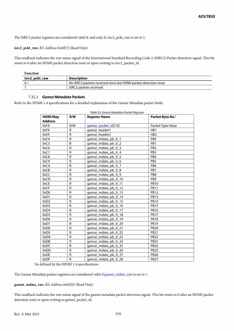
ADV7850
Rev. A May 2012 210
The ISRC2 packet registers are considered valid if, and only if, isrc2_pckt_raw is set to 1. isrc2_pckt_raw, IO, Address 0x60[7] (Read Only) This readback indicates the raw status signal of the International Standard Recording Code 2 (ISRC2) Packet detection signal. This bit resets to 0 after an HDMI packet detection reset or upon writing to isrc2_packet_id.
Function isrc2_pckt_raw Description 0 No ISRC2 packets received since last HDMI packet detection reset 1 ISRC2 packets received
7.35.3 Gamut Metadata Packets Refer to the HDMI 1.4 specifications for a detailed explanation of the Gamut Metadata packet fields.
Table 33: Gamut Metadata Packet Registers HDMI Map Address
R/W Register Name Packet Byte No.1
0xF8 R/W gamut_packet_id[7:0] Packet Type Value 0xF9 R gamut_header1 HB1 0xFA R gamut_header2 HB2 0xC4 R gamut_mdata_pb_0_1 PB0 0xC5 R gamut_mdata_pb_0_2 PB1 0xC6 R gamut_mdata_pb_0_3 PB2 0xC7 R gamut_mdata_pb_0_4 PB3 0xC8 R gamut_mdata_pb_0_5 PB4 0xC9 R gamut_mdata_pb_0_6 PB5 0xCA R gamut_mdata_pb_0_7 PB6 0xCB R gamut_mdata_pb_0_8 PB7 0xCC R gamut_mdata_pb_0_9 PB8 0xCD R gamut_mdata_pb_0_10 PB9 0xCE R gamut_mdata_pb_0_11 PB10 0xCF R gamut_mdata_pb_0_12 PB11 0xD0 R gamut_mdata_pb_0_13 PB12 0xD1 R gamut_mdata_pb_0_14 PB13 0xD2 R gamut_mdata_pb_0_15 PB14 0xD3 R gamut_mdata_pb_0_16 PB15 0xD4 R gamut_mdata_pb_0_17 PB16 0xD5 R gamut_mdata_pb_0_18 PB17 0xD6 R gamut_mdata_pb_0_19 PB18 0xD7 R gamut_mdata_pb_0_20 PB19 0xD8 R gamut_mdata_pb_0_21 PB20 0xD9 R gamut_mdata_pb_0_22 PB21 0xDA R gamut_mdata_pb_0_23 PB22 0xDB R gamut_mdata_pb_0_24 PB23 0xDC R gamut_mdata_pb_0_25 PB24 0xDD R gamut_mdata_pb_0_26 PB25 0xDE R gamut_mdata_pb_0_27 PB26 0xDF R gamut_mdata_pb_0_28 PB27
1As defined by the HDMI 1.4 specifications The Gamut Metadata packet registers are considered valid if gamut_mdata_raw is set to 1. gamut_mdata_raw, IO, Address 0x65[0] (Read Only) This readback indicates the raw status signal of the gamut metadata packet detection signal. This bit resets to 0 after an HDMI packet detection reset or upon writing to gamut_packet_id.

ADV7850
Rev. A May 2012 211
Function gamut_mdata_raw Description 0 No gamut metadata packet received in last video frame or since last HDMI packet detection
reset 1 Gamut metadata packet received in last video frame
gamut_irq_next_field, Addr 68 (HDMI), Address 0x50[4] This control is used to set the new_gamut_mdata_raw interrupt to detect when the new contents are applicable to the next field or to indicate that the gamut packet is new. This is done using the header information of the gamut packet.
Function gamut_irq_next_field Description 0 Interrupt flag indicates that gamut packet is new 1 Interrupt flag indicates that gamut packet is to be applied to next field
7.36 CUSTOMIZING PACKET/INFOFRAME STORAGE REGISTERS The packet type value of each set of packet and InfoFrame registers in the InfoFrame Map is programmable. This allows the user to configure the ADV7850 to store the payload data of any packet and InfoFrames sent by the transmitter connected on the selected HDMI port. Note: Writing to any of the nine following packet ID registers also clears the corresponding raw InfoFrame/packet detection bit. For example, writing 0x82, or any other value, to avi_packet_id clears avi_info_raw. avi_packet_id[7:0], Addr 7C (InfoFrame), Address 0xE0[7:0] This control is used to set the AVI InfoFrame ID.
Function avi_packet_id[7:0] Description 0xxxxxxx Packet type value of packet stored in InfoFrame Map, Address 0x00 to 0x1B 1xxxxxxx Packet type value of InfoFrame stored in InfoFrame Map, Address 0x00 to 0x1B
aud_packet_id[7:0], Addr 7C (InfoFrame), Address 0xE3[7:0] This control is used to set the audio InfoFrame ID.
Function aud_packet_id[7:0] Description 0xxxxxxx Packet type value of packet stored in InfoFrame Map, Address 0x1C to 0x29 1xxxxxxx Packet type value of InfoFrame stored in InfoFrame Map, Address 0x1C to 0x29
spd_packet_id[7:0], Addr 7C (InfoFrame), Address 0xE6[7:0] This control is used to set the Source Product Descriptor InfoFrame ID.
Function spd_packet_id[7:0] Description 0xxxxxxx Packet type value of packet stored in InfoFrame Map, Address 0x2A to 0x45 1xxxxxxx Packet type value of InfoFrame stored in InfoFrame Map, Address 0x2A to 0x45

ADV7850
Rev. A May 2012 212
ms_packet_id[7:0], Addr 7C (InfoFrame), Address 0xE9[7:0] This control is used to set the MPEG source InfoFrame ID.
Function ms_packet_id[7:0] Description 0xxxxxxx Packet type value of packet stored in InfoFrame Map, Address 0x46 to 0x53 1xxxxxxx Packet type value of InfoFrame stored in InfoFrame Map, Address 0x46 to 0x53
vs_packet_id[7:0], Addr 7C (InfoFrame), Address 0xEC[7:0] This control is used to set the Vendor Specific InfoFrame ID.
Function vs_packet_id[7:0] Description 0xxxxxxx Packet type value of packet stored in InfoFrame Map, Address 0x54 to 0x6F 1xxxxxxx Packet type value of packet stored in InfoFrame Map, Address 0x54 to 0x6F
acp_packet_id[7:0], Addr 7C (InfoFrame), Address 0xEF[7:0] This control is used to set the ACP packet ID.
Function acp_packet_id[7:0] Description 0xxxxxxx Packet type value of packet stored in InfoFrame Map, Address 0x70 to 0x8B 1xxxxxxx Packet type value of InfoFrame stored in InfoFrame Map, Address 0x70 to 0x8B
isrc1_packet_id[7:0], Addr 7C (InfoFrame), Address 0xF2[7:0] This control is used to set the ISRC1 packet ID.
Function isrc1_packet_id[7:0] Description 0xxxxxxx Packet type value of packet stored in InfoFrame Map, Address 0x8C to 0xA7 1xxxxxxx Packet type value of InfoFrame stored in InfoFrame Map, Address 0x8C to 0xA7
isrc2_packet_id[7:0], Addr 7C (InfoFrame), Address 0xF5[7:0] This control is used to set the ISRC2 packet ID.
Function isrc2_packet_id[7:0] Description 0xxxxxxx Packet type value of packet stored in InfoFrame Map, Address 0xA8 to 0xC3 1xxxxxxx Packet type value of InfoFrame stored in InfoFrame Map, Address 0xA8 to 0xC3
gamut_packet_id[7:0], Addr 7C (InfoFrame), Address 0xF8[7:0] This control is used to set the gamut metadata packet ID.
Function gamut_packet_id[7:0] Description 0xxxxxxx Packet type value of packet stored in InfoFrame Map, Address 0xC4 to 0xDF 1xxxxxxx Packet type value of InfoFrame stored in InfoFrame Map, Address 0xC4 to 0xDF
Note: The packet type values and corresponding packets should not be programmed in the packet type values registers. These packets are always processed internally and cannot be stored in the packet/InfoFrame registers in the InfoFrame Map:

ADV7850
Rev. A May 2012 213
• 0x01: Audio Clock Regeneration Packet • 0x02: Audio Sample Packet • 0x03: General Control Packet • 0x07: DSD Audio Sample Packet • 0x08: DST Audio Sample Packet • 0x09: HBR Audio Stream Packet
7.37 BACKGROUND PORT INFOFRAME AND PACKET SUPPORT The ADV7850 can provide limited information on the packets received on the background port via the following controls and readback registers. bg_header_requested[7:0], Addr 68 (HDMI), Address 0xEF[7:0] This control is used to select the type of InfoFrame/packet to be provided for readback in the background port header and packet registers (0xF0 to 0xF5). The value set in this register is compared against the detected InfoFrame or packet header byte 0. If they match, header byte 1 and data bytes 1 to 5 are stored. The default value of 0x82 is the InfoFrame type of the AVI InfoFrame.
Function bg_header_requested[7:0]
Description
xxxxxxxx Header value requested. This will be compared with detected packet headers. If a match is found, data is stored in registers 0xF0 to 0xF5.
bg_header_byte1[7:0], Addr 68 (HDMI), Address 0xF0[7:0] (Read Only) This readback displays byte 1 of the header for the InfoFrame/packet selected to be read in the background port.
Function bg_header_byte1[7:0] Description xxxxxxxx Header byte 1 data. Only valid if bg_valid_packet is high.
bg_packet_byte1[7:0], Addr 68 (HDMI), Address 0xF1[7:0] (Read Only) This readback displays byte 1 of the packet for the InfoFrame/packet selected to be read in the background port.
Function bg_packet_byte1[7:0] Description xxxxxxxx Packet byte 1 data. Only valid if bg_valid_packet is high.
bg_packet_byte2[7:0], Addr 68 (HDMI), Address 0xF2[7:0] (Read Only) This readback displays byte 2 of the packet for the InfoFrame/packet selected to be read in the background port.
Function bg_packet_byte2[7:0] Description xxxxxxxx Packet byte 2 data. Only valid if bg_valid_packet is high.
bg_packet_byte3[7:0], Addr 68 (HDMI), Address 0xF3[7:0] (Read Only) This readback displays byte 3 of the packet for the InfoFrame/packet selected to be read in background port.

ADV7850
Rev. A May 2012 214
Function bg_packet_byte3[7:0] Description xxxxxxxx Packet byte 3 data. Only valid if bg_valid_packet is high.
bg_packet_byte4[7:0], Addr 68 (HDMI), Address 0xF4[7:0] (Read Only) This readback displays byte 4 of the packet for the InfoFrame/packet selected to be read in the background port.
Function bg_packet_byte4[7:0] Description xxxxxxxx Packet byte 4 data. Only valid if bg_valid_packet is high.
bg_packet_byte5[7:0], Addr 68 (HDMI), Address 0xF5[7:0] (Read Only) This readback displays byte 5 of the packet for the InfoFrame/packet selected to be read in the background port.
Function bg_packet_byte5[7:0] Description xxxxxxxx Packet byte 5 data . Only valid if bg_valid_packet is high.
bg_valid_packet, Addr 68 (HDMI), Address 0xF6[0] (Read Only) This readback indicates if the background header and packet information is valid.
Function bg_valid_packet Description 0 Background header and packet readbacks not valid 1 Background header and packet readbacks valid
7.38 REPEATER SUPPORT The ADV7850 incorporates an E-EDID/Repeater controller that provides all the features required for a receiver front end of a fully HDCP 1.3 compliant repeater system. The ADV7850 has a RAM that can store up to 128 KSVs, which allows it to handle up to 128 downstream devices in repeater mode. Refer to Table 34. The ADV7850 features a set of HDCP registers, defined in the HDCP specifications, which are accessible through the DDC bus (refer to Section 14.2) of the selected port. A subset of the HDCP registers (defined in the following subsections) are also available in the Repeater Map and are accessible through the main I2C port (refer to Section 14.1).
7.38.1 Repeater Routines Performed by the E-EDID/Repeater Controller 1. Power Up
A power-on reset circuitry on the DVDD supply is used to reset the E-EDID/Repeater controller when the ADV7850 is powered up. When the E-EDID/Repeater controller reboots after reset, it resets all the KSV registers listed in Table 34.
2. AKSV Update
The E-EDID/Repeater controller resets automatically the bcaps[5] bit to 0 when an HDCP transmitter writes its AKSV into the ADV7850 HDCP registers through the DDC bus of the selected HDMI port.
Note: Writing a value in the aksv[39:32] triggers an AKSV update and aksv_update_st interrupt if either aksv_update_mb1 or aksv_update_mb2 is set to 1. This triggers the E-EDID/Repeater controller to reset the bcaps[5] bit back to 0.
3. KSV List Ready
The ksv_list_ready bit is set by an external controller driving the ADV7850. This notifies the ADV7850 on-chip E-EDID/Repeater

ADV7850
Rev. A May 2012 215
controller that the KSV list registers have been updated with the KSVs of the attached and active downstream HDCP devices. When ksv_list_ready is set to 1, the E-EDID/Repeater controller computes the SHA-1 hash value V’, updates the corresponding V’ registers (refer to Table 34), and sets the ready bit (that is, bit [5] of bcaps[7:0]) to 1. This indicates to the transmitter attached to the ADV7850 that the KSV FIFO and SHA-1 hash value V’ are ready to be read.
ksv_list_ready, Addr 64 (Repeater), Address 0x71[7] The system sets this bit in order to indicate that the KSV list has been read from the Tx IC(s) and written into the Repeater Map. The system must also set bits [11:0] of Bstatus before setting this bit.
Function ksv_list_ready Description 0 Not ready 1 Ready
Notes:
• The SHA-1 hash value will be computed if ksv_list_ready is set after the part has received an AKSV update from the upstream source. The external controller should, therefore, set ksv_lst_ready to 1 only after the part has received an AKSV update from the upstream source.
• The ADV7850 does not automatically clear ksv_list_ready to 0 after it has finished computing the SHA-1 value. Therefore, the external controller needs to clear ksv_list_ready.
4 HDMI Mode Bit [12] of bstatus[15:0] is updated automatically by the ADV7850 and follows the status of the HDMI mode (refer to hdmi_mode) of the HDMI/DVI stream input on the active HDMI port. Bit [12] of bstatus[15:0] is set to 1 if the ADV7850 receives an HDMI stream, and set to 0 if the ADV7850 receives a DVI stream.
7.38.2 Repeater Actions Required by External Controller The external controller must set the bcaps register and notify the ADV7850 when the KSV list is updated, as described in the following actions 1 to 4. Note that many more routines must be implemented into the external controller driving the ADV7850 to implement a full repeater. Such routines are described in the HDCP and HDMI specifications (for example, copying InfoFrame and packet data images from the HDMI receiver into the HDMI transmitter, momentarily de-asserting the hot plug detect and disabling the clock termination on a change of downstream topology, and so on). 1. Repeater Bit
The repeater bit (that is, Bit [6] of bcaps[7:0] must be set to 1 by the external controller in the routine that initializes the ADV7850. The repeater bit must be left as such as long as the ADV7850 is configured as the front end of a repeater system. Note: The registers in the KSV list (refer to Table 34) should always be set to 0x0 if the repeater bit is set to 0. The firmware running on the external controller, therefore, always sets the registers in the KSV list to 0x0 if the repeater bit is changed from 1 to 0.
2. KSV FIFO Read from HDCP Registers
The KSV FIFO read at address 0x43 through the HDCP port of the selected HDMI port is dependent on the value of the repeater bit (that is, bit [6] of bcaps[7:0]):
• When the repeater bit is set to 0, the KSV FIFO read from the HDCP port always returns 0x0 • When the repeater bit is set to 1, the KSV FIFO read from the HDCP port matches the KSV list which is set in the Repeater
Map at addresses 0x80 to 0xF7 (refer to Table 34)
3. First AKSV Update When the upstream transmitter writes its AKSV for the first time into the ADV7850 HDCP registers, the external controller driving the ADV7850 should perform the following tasks:

ADV7850
Rev. A May 2012 216
• Update bits [11:0] of bstatus[15:0] according to the topology of the downstream device attached to the repeater. • Update the KSV list (refer to Table 34) with the KSV from the transmitter on the back end of the repeater as well as the KSV
from all the downstream devices connected to the repeater. • Set ksv_list_ready to 1. • The external controller can monitor the aksv_update_x_raw bits to be notified when the transmitter writes its AKSV into
the HDCP registers of the ADV7850 (where x is A, B, C or D). aksv_update_a_raw, IO, Address 0x88[3] (Read Only) Status of Port A AKSV update interrupt signal. When set to 1, it indicates that transmitter has written its AKSV into HDCP registers for Port A. Once set, this bit remains high until it is cleared via aksv_update_a_clr.
Function aksv_update_a_raw Description 0 No AKSV updates on Port A 1 Detected a write access to the AKSV register on Port A
aksv_update_b_raw, IO, Address 0x88[2] (Read Only) This readback displays the status of the Port B AKSV update interrupt signal. When set to 1, it indicates that the transmitter has written its AKSV into the HDCP registers for Port B. Once set, this bit remains high until it is cleared via aksv_update_b_clr.
Function aksv_update_b_raw Description 0 No AKSV updates on Port B 1 Detected write access to AKSV register on Port B
aksv_update_c_raw, IO, Address 0x88[1] (Read Only) This readback displays the status of the Port C AKSV update interrupt signal. When set to 1, it indicates that the transmitter has written its AKSV into the HDCP registers for Port C. Once set, this bit remains high until it is cleared via aksv_update_c_clr.
Function aksv_update_c_raw Description 0 No AKSV updates on Port C 1 Detected write access to AKSV register on Port C
aksv_update_d_raw, IO, Address 0x88[0] (Read Only) This readback displays the status of the Port D AKSV update interrupt signal. When set to 1, it indicates that the transmitter has written its AKSV into the HDCP registers for Port D. Once set, this bit remains high until it is cleared via aksv_update_d_clr.
Function aksv_update_d_raw Description 0 No AKSV updates on Port D 1 Detected write access to AKSV register on Port D
4. Second and Subsequent AKSV Updates
When the upstream transmitter writes its AKSV for the second time or more into the ADV7850 HDCP registers, the external controller driving the ADV7850 should set ksv_list_ready to 1.
7.38.3 HDCP Registers Available in Repeater Map In order to enable fast switching of the HDCP encrypted HDMI ports, the registers 0x00 to 0x42 in the Repeater Map are replicated for each port. auto_hdcp_map_enable and hdcp_map_select[2:0] determine which port is currently visible to the user.

ADV7850
Rev. A May 2012 217
auto_hdcp_map_enable, Addr 64 (Repeater), Address 0x79[3] This control is used to select the port to be accessed for HDCP addresses, i.e. the HDMI active port (selected by hdcp_port_select in the HDMI Map), or the port selected in hdcp_map_select.
Function auto_hdcp_map_enable
Description
0 HDCP data read from port given by hdcp_map_select 1 HDCP data read from the active HDMI port
hdcp_map_select[2:0], Addr 64 (Repeater), Address 0x79[2:0] This control is used to select the port to be accessed for HDCP addresses (0x00 to 0x42 in the Repeater Map). This only takes effect when auto_hdcp_man_enable is set to 0.
Function hdcp_map_select[2:0] Description 000 Select Port A 001 Select Port B 010 Select Port C 011 Select Port D
bksv[39:0], Addr 64 (Repeater), Address 0x04[7:0]; Address 0x03[7:0]; Address 0x02[7:0]; Address 0x01[7:0]; Address 0x00[7:0] (Read Only) The HDMI receiver Key Selection Vector (bksv) can be read back once the part has successfully accessed the HDCP ROM. The following registers contain the bksv read from the EEPROM: 0x00[7:0] = bksv[7:0], 0x01[7:0] = bksv[15:8], 0x02[7:0 ] = bksv[23:16], 0x03[7:0] = bksv[31:24] and 0x04[7:0] = bksv[39:32]. aksv[39:0], Addr 64 (Repeater), Address 0x14[7:0]; Address 0x13[7:0]; Address 0x12[7:0]; Address 0x11[7:0]; Address 0x10[7:0] This readback indicates the aksv value. The aksv of the transmitter attached to the active HDMI port can be read back after an aksv update. The following registers contain the aksv written by the Tx. 0x10[7:0] = aksv[7:0], 0x11[7:0] = aksv[15:8], 0x12[7:0] = aksv[23:16], 0x13[7:0] = aksv[31:24] and 0x14[7:0] = aksv[39:32]. bcaps[7:0], Addr 64 (Repeater), Address 0x40[7:0] This control is used to set the bcaps register which is presented to the TX attached to the active HDMI port.
Function bcaps[7:0] Description 10000011 Default bcaps register value presented to the Tx xxxxxxxx bcaps register value presented to the Tx
bstatus[15:0], Addr 64 (Repeater), Address 0x42[7:0]; Address 0x41[7:0] This control is used to set the bstatus information presented to the active HDMI port. Bits [11:0] must be set by the system software acting as a repeater. 0x41[7:0] = bstatus[7:0], 0x42[7:0] = bstatus[15:8].

ADV7850
Rev. A May 2012 218
Function bstatus[15:0] Description xxxxxxxxxxxxxxxx bstatus register presented to Tx 0000000000000000 Reset value. bstatus register is reset only after power up.
Table 34: Register Location for SHA_1 Hash Value Register Name Address Location1 Function sha_a[31:0] 0x20[7:0]: sha_a[7:0]
0x21[7:0]: sha_a[15:8] 0x22[7:0]: sha_a[23:16] 0x23[7:0]: sha_a[31:24]
H0 part of SHA-1 hash value V’. Register also called (v’.h1)2
sha_b[31:0] 0x24[7:0]: sha_b[7:0] 0x25[7:0]: sha_b[15:8] 0x26[7:0]: sha_b[23:16] 0x27[7:0]: sha_b[31:24]
H1 part of SHA-1 hash value V’. Register also called (v’.h1)2
sha_c[31:0] 0x28[7:0]: sha_c[7:0] 0x29[7:0]: sha_c[15:8] 0x2a[7:0]: sha_c[23:16] 0x2b[7:0]: sha_c[31:24]
H2 part of SHA-1 hash value V’. Register also called (v’.h2)2
sha_d[31:0] 0x2c[7:0]: sha_d[7:0] 0x2d[7:0]: sha_d[15:8] 0x2e[7:0]: sha_d[23:16] 0x2f[7:0]: sha_d[31:24]
H3 part of SHA-1 hash value V’. Register also called (v’.h3)2
sha_e[31:0] 0x30[7:0]: sha_e[7:0] 0x31[7:0]: sha_e[15:8] 0x32[7:0]: sha_e[23:16] 0x33[7:0]: sha_e[31:24]
H4 part of SHA-1 hash value V’. Register also called (v’.h4)2
1All registers specified in table are located in the Repeater Map 2 Refer to HDCP Protection System Standards The ADV7850 supports up to 25 KSVs (0 through to 24). The complete set of bytes is listed below. Each KSV is 40bits long and the first KSV starts at address 0x80.
Table 35: KSV List Bytes KSV Byte Register Name Address1
0 ksv_byte0 80
1 ksv_byte1 81
2 ksv_byte2 82
3 ksv_byte3 83
4 ksv_byte4 84
5 ksv_byte5 85
6 ksv_byte6 86
7 ksv_byte7 87
8 ksv_byte8 88
9 ksv_byte9 89
10 ksv_byte10 8A
11 ksv_byte11 8B
12 ksv_byte12 8C
13 ksv_byte13 8D
14 ksv_byte14 8E
15 ksv_byte15 8F
16 ksv_byte16 90
17 ksv_byte17 91

ADV7850
Rev. A May 2012 219
KSV Byte Register Name Address1
18 ksv_byte18 92
19 ksv_byte19 93
20 ksv_byte20 94
21 ksv_byte21 95
22 ksv_byte22 96
23 ksv_byte23 97
24 ksv_byte24 98
25 ksv_byte25 99
26 ksv_byte26 9A
27 ksv_byte27 9B
28 ksv_byte28 9C
29 ksv_byte29 9D
30 ksv_byte30 9E
31 ksv_byte31 9F
32 ksv_byte32 A0
33 ksv_byte33 A1
34 ksv_byte34 A2
35 ksv_byte35 A3
36 ksv_byte36 A4
37 ksv_byte37 A5
38 ksv_byte38 A6
39 ksv_byte39 A7
40 ksv_byte40 A8
41 ksv_byte41 A9
42 ksv_byte42 AA
43 ksv_byte43 AB
44 ksv_byte44 AC
45 ksv_byte45 AD
46 ksv_byte46 AE
47 ksv_byte47 AF
48 ksv_byte48 B0
49 ksv_byte49 B1
50 ksv_byte50 B2
51 ksv_byte51 B3
52 ksv_byte52 B4
53 ksv_byte53 B5
54 ksv_byte54 B6
55 ksv_byte55 B7
56 ksv_byte56 B8
57 ksv_byte57 B9
58 ksv_byte58 BA
59 ksv_byte59 BB
60 ksv_byte60 BC
61 ksv_byte61 BD

ADV7850
Rev. A May 2012 220
KSV Byte Register Name Address1
62 ksv_byte62 BE
63 ksv_byte63 BF
64 ksv_byte64 C0
65 ksv_byte65 C1
66 ksv_byte66 C2
67 ksv_byte67 C3
68 ksv_byte68 C4
69 ksv_byte69 C5
70 ksv_byte70 C6
71 ksv_byte71 C7
72 ksv_byte72 C8
73 ksv_byte73 C9
74 ksv_byte74 CA
75 ksv_byte75 CB
76 ksv_byte76 CC
77 ksv_byte77 CD
78 ksv_byte78 CE
79 ksv_byte79 CF
80 ksv_byte80 D0
81 ksv_byte81 D1
82 ksv_byte82 D2
83 ksv_byte83 D3
84 ksv_byte84 D4
85 ksv_byte85 D5
86 ksv_byte86 D6
87 ksv_byte87 D7
88 ksv_byte88 D8
89 ksv_byte89 D9
90 ksv_byte90 DA
91 ksv_byte91 DB
92 ksv_byte92 DC
93 ksv_byte93 DD
94 ksv_byte94 DE
95 ksv_byte95 DF
96 ksv_byte96 E0
97 ksv_byte97 E1
98 ksv_byte98 E2
99 ksv_byte99 E3
100 ksv_byte100 E4
101 ksv_byte101 E5
102 ksv_byte102 E6
103 ksv_byte103 E7
104 ksv_byte104 E8
105 ksv_byte105 E9

ADV7850
Rev. A May 2012 221
KSV Byte Register Name Address1
106 ksv_byte106 EA
107 ksv_byte107 EB
108 ksv_byte108 EC
109 ksv_byte109 ED
110 ksv_byte110 EE
111 ksv_byte111 EF
112 ksv_byte112 F0
113 ksv_byte113 F1
114 ksv_byte114 F2
115 ksv_byte115 F3
116 ksv_byte116 F4
117 ksv_byte117 F5
118 ksv_byte118 F6
119 ksv_byte119 F7
120 ksv_byte120 F8
121 ksv_byte121 F9
122 ksv_byte122 FA
123 ksv_byte123 FB
124 ksv_byte124 FC
125 ksv_byte125 FD
126 ksv_byte126 FE
127 ksv_byte127 FF 1All registers specified in table are located in the Repeater Map.
7.39 INTERFACE TO DCM SECTION The video data from the HDMI section is sent to the CP section via the DCM block. The video data output by the HDMI section is always in a 4:4:4 format with 36 bits per pixel. This is irrespective of the encoding format of the video data encapsulated in the HDMI/DVI stream input to the HDMI receiver section (that is, 4:2:2 or 4:4:4).
• If the HDMI section receives a stream with video encoded in a 4:4:4 format, it passes the video data to the DCM section. • If the HDMI section receives a stream with video encoded in a 4:2:2 format (refer to Figure 74), the HDMI section upconverts
the video data into a 4:4:4 format, according to the up_conversion_mode bit, and passes the upconverted video data to the DCM section (refer to Figure 75).
• If the HDMI receiver receives video data with fewer than 12 bits used per channel, the valid bits are left-shifted on each component channel with zeroes padding the bit below the LSB before being sent to the DCM section.
Figure 74: YCbCr 4:2:2 Video Data Encapsulated in HDMI Stream
Y0 bits 3-0
Cb0 bits 3-0
Y1 bits 3-0
Cr0 bits 3-0
Y2 bits 3-0
Cb2 bits 3-0
Y3 bits 3-0
Cr2 bits 3-0
Y4 bits 3-0
Cb4 bits 3-0
...
...
Y0 bits 11-4 Y
1 bits 11-4 Y
2 bits 11-4 Y
3 bits 11-4 Y
4 bits 11-4 ...
Cb0 bits 11-4 Cr
0 bits 11-4 Cb
2 bits 11-4 Cr
2 bits 11-4 Cb
4 bits 11-4 ...
Bit 7-4
Bit 3-0
Bit 7-0
Bit 7-0
TMDSChannel
Y0 / Cb0 Y1 / Cr0 Y2 / Cb2 Y3 / Cr2 Y4 / Cb4...
1
2
0
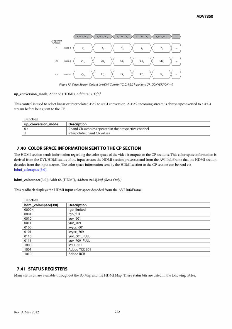
ADV7850
Rev. A May 2012 222
Figure 75: Video Stream Output by HDMI Core for YCbCr 4:2:2 Input and UP_CONVERSION = 0 up_conversion_mode, Addr 68 (HDMI), Address 0x1D[5] This control is used to select linear or interpolated 4:2:2 to 4:4:4 conversion. A 4:2:2 incoming stream is always upconverted to a 4:4:4 stream before being sent to the CP.
Function up_conversion_mode Description 0 Cr and Cb samples repeated in their respective channel 1 Interpolate Cr and Cb values
7.40 COLOR SPACE INFORMATION SENT TO THE CP SECTION The HDMI section sends information regarding the color space of the video it outputs to the CP sections. This color space information is derived from the DVI/HDMI status of the input stream the HDMI section processes and from the AVI InfoFrame that the HDMI section decodes from the input stream. The color space information sent by the HDMI section to the CP section can be read via hdmi_colorspace[3:0]. hdmi_colorspace[3:0], Addr 68 (HDMI), Address 0x53[3:0] (Read Only) This readback displays the HDMI input color space decoded from the AVI InfoFrame.
Function hdmi_colorspace[3:0] Description 0000 rgb_limited 0001 rgb_full 0010 yuv_601 0011 yuv_709 0100 xvycc_601 0101 xvycc_709 0110 yuv_601_FULL 0111 yuv_709_FULL 1000 sYCC 601 1001 Adobe YCC 601 1010 Adobe RGB
7.41 STATUS REGISTERS Many status bit are available throughout the IO Map and the HDMI Map. These status bits are listed in the following tables.
Cb0
Cb0
Cb2
Cb2
Cb4
...
Cr0
Cr0
Cr2
Cr2
Cr4
...
Bit 12-0
Bit 12-0
ComponentChannel
Y0 / Cb0 / Cr0 Y1 / Cb0 / Cr0 Y2/ Cb2 / Cr2 Y3 / Cb2 / Cr2 Y4 / Cb4 / Cr4...
Cb
Cr
Y Y0
Y1
Y2
Y3
Y4
...Bit 12-0

ADV7850
Rev. A May 2012 223
Table 36: HDMI Flags in IO Map Register 0x60
Bit Name Bit Position
Description
avi_info_raw 0 (LSB) Returns 1 if AVI InfoFrame received within last seven VSyncs. audio_info_raw 1 Returns 1 if AVI InfoFrame received within last three VSync. Additional description available on page 203. spd_info_raw 2 Returns 1 if SPD InfoFrame received. Additional description available on page 204. ms_info_raw 3 Returns 1 if MPEG InfoFrame received within last three VSync. Additional description available on page
205. vs_info_raw 4 Returns 1 if Vendor Specific InfoFrame received. Additional description available on page 206. acp_pckt_raw 5 Returns 1 if ACP packet received within last 600 ms. Additional description available on page 208. isrc1_pckt_raw 6 Returns 1 if ISRC1 packet received. Additional description available on page 209. isrc2_pckt_raw 7 (MSB) Returns 1 if ISRC2 packet received. Additional description available on page 210.
Table 37: HDMI Flags in IO Map Register 0x65 Bit Name Bit
Position Description
gamut_mdata_raw 0 (LSB) Returns 1 if Gamut Metadata packet received. Additional description available on page 210. audio_c_pckt_raw 1 Returns 1 if audio clock regeneration packet received. Reset to 0 following a packet detection flag reset
condition. (Refer to Section 7.43.) gen_ctl_pckt_raw 2 Returns 1 if general control packet received. Reset to 0 following a packet detection flag reset condition.
(Refer to Section 7.43.) hdmi_mode_raw 3 Returns 1 if a HDMI stream is being received. Additional description available on page 153. audio_ch_md_raw 4 Returns 1 if audio channel mode is multi-channel (2, 4, 6 or 8 channel) audio. Reset to 0 following a
packet detection flag reset condition. (Refer to Section 7.43.) Additional description available on page 191.
av_mute_raw 5 Returns 1 if latest general control packet received has av_mute asserted. Reset to 0 following a packet detection flag reset condition. (Refer to Section 7.43.)
internal_mute_raw 6 Returns 1 if ADV7850 has internally muted the audio data. Additional information available on page 194. cs_data_valid_raw 7 (MSB) Returns 1 if channel status bit readback registers in HDMI Map, Address 0x36 to 0x3A are valid.
Additional information available on page 196.
Table 38: HDMI Flags in IO Map Register 0x6A Bit Name Bit Position Description tmds_clk_d_raw 0 (LSB) Description available on page 154 tmds_clk_c_raw 1 Description available on page 154 tmds_clk_b_raw 2 Description available on page 154 tmds_clk_a_raw 3 Description available on page 153 tmdspll_lck_d_raw 4 Description available on page 157 tmdspll_lck_c_raw 5 Description available on page 157 tmdspll_lck_b_raw 6 Description available on page 157 tmdspll_lck_a_raw 7 (MSB) Description available on page 157
Table 39: HDMI Flags in IO Map Register 0x6F
Bit Name Bit Position Description cable_det_d_raw 0 (LSB) Description available on page 137 cable_det_c_raw 1 Description available on page 137 cable_det_b_raw 2 Description available on page 137 cable_det_a_raw 3 Description available on page 137 hdmi_encrpt_d_raw 4 Description available on page 166 hdmi_encrpt_c_raw 5 Description available on page 166 hdmi_encrpt_b_raw 6 Description available on page 166 hdmi_encrpt_a_raw 7 (MSB) Description available on page 166
Table 40: HDMI Flags in IO Map Register 0x74
Bit Name Bit Position Description de_regen_lck_raw 0 (LSB) Description available on page 170 v_locked_raw 1 Description available on page 173 video_3d_raw 2 3D Video Detected RAW status bit

ADV7850
Rev. A May 2012 224
Table 41: HDMI Flags in IO Map Register 0x79 Bit Name Bit Position new_avi_info_raw 0 (LSB) new_audio_info_raw 1 new_spd_info_raw 2 new_ms_info_raw 3 new_vs_info_raw 4 new_acp_pckt_raw 5 new_isrc1_pckt_raw 6 new_isrc2_pckt_raw 7 (MSB)
Table 42: HDMI Flags in IO Map Register 0x7E Bit Name Bit
Position Description
new_gamut_mdata_raw 0 (LSB) When set to 1, indicates that Gamut Metadata packet with new content received. Once set, remains high until interrupt cleared via new_gamut_mdata_pckt_clr (IO Map 0x80 [0]).
audio_pckt_err_raw 1 When set to 1, indicates that an uncorrectable error detected in body of an audio packet. Once set, remains high until interrupt cleared via audio_pckt_err_clr (IO Map 0x80 [1]).
packet_error_raw 2 When set to 1, indicates an uncorrectable EEC error detected in body or header of any packet. Once set, remains high until interrupt cleared via packet_error_clr (IO Map 0x80 [2]).
change_n_raw 3 When set to 1, indicates the N value of the ACR packets changed. Once set, remains high until interrupt cleared via change_n_clr (IO Map 0x80 [3]).
cts_pass_thrsh_raw
4 When set to 1, indicates the CTS value of the ACR packets exceeded threshold set by cts_change_threshold. Once set, remains high until interrupt cleared via cts_pass_thrsh_clr (IO Map 0x80 [4]).
fifo_overflo_raw 5 When set to 1, indicates the audio FIFO write pointer reached the read pointer causing audio FIFO to overflow. Once set, remains high until interrupt cleared via fifo_overflo_clr (IO Map 0x80 [5]).
fifo_underflo_raw
6 When set to 1, indicates the audio FIFO read pointer reached the write pointer causing audio FIFO to underflow. Once set, remains high until interrupt cleared via fifo_underflo_clr (IO Map 0x80 [6]).
fifo_near_ovfl_raw 7 (MSB) When set to 1, indicates the audio FIFO is near overflow as the number of FIFO registers containing stereo data is greater or equal to value set in audio_fifo_almost_full_threshold. Once set, remains high until interrupt cleared via fifo_near_ovfl_clr (IO Map 0x80 [7]).
Table 43: HDMI Flags in IO Map Register 0x83
Bit Name Bit Position
Description
fifo_near_uflo_raw
0 (LSB) When set to 1, indicates audio FIFO is near underflow as the number of FIFO registers containing stereo data is less or equal to value set in audio_fifo_almost_empty_threshold. Once set, remains high until interrupt cleared via fifo_near_uflo_clr (IO Map 0x85 [0]).
new_tmds_frq_raw 1 When set to 1, indicates the TMDS Frequency has changed by more than the tolerance set in freqtolerance[3:0]. Once set, remains high until interrupt cleared via new_tmds_freq_clr (IO Map 0x85 [1]).
audio_flt_line_raw 2 When set to 1, indicates audio sample packet received with Flat line bit set to 1. Once set, remains high until interrupt cleared via audio_flt_line_clr (IO Map 0x85 [2]).
new_samp_rt_raw 3 When set to 1, indicates that audio sampling frequency field in channel status data has changed. Once set, remains high until interrupt cleared via new_samp_rt_clr (IO Map 0x85 [3]).
parity_error_raw 4 When set to 1, indicates an audio sample packet received with parity error. Once set, remains high until interrupt cleared via parity_error_clr (IO Map 0x85 [4]).
audio_mode_chng_raw 5 When set to 1, indicates the type of audio packet received has changed. The following are considered audio modes: No Audio, PCM, DSD, DST or HBR. audio_sample_pckt_det, dsd_packet_det, dst_packet_det and hbr_audio_pckt_det used to identify type of audio packet currently received. Once set, remains high until the interrupt cleared via audio_mode_chng_clr (IO Map 0x85 [5]).
vclk_chng_raw 6 When set to 1, indicates that irregular or missing pulses are detected in the TMDS clock. Once set, remains high until interrupt cleared via vclk_chng_clr (IO Map 0x85 [6]).
deep_color_chng_raw 7 (MSB) When set to 1, indicates a change in the deep color mode detected. Once set, remains high until interrupt has been cleared via deep_color_chng_clr (IO Map 0x85 [7]).
ADV7850
Rev. A May 2012 225
Table 44: HDMI InfoFrame Checksum Error Flags in IO Map Bit Name IO Map Location Description avi_inf_cks_err_raw 0x88[4] Description available on page 201 aud_inf_cks_err_raw 0x88[5] Description available on page 201 spd_inf_cks_err_raw 0x88[6] Description available on page 201 ms_inf_cks_err_raw 0x88[7] Description available on page 202 vs_inf_cks_err_raw 0x8D[0] Description available on page 202
Table 45: AKSV Update Flags in IO Map Register 0x88
Bit Name Bit Position
Description
aksv_update_d_raw 0 (LSB) When set to 1, indicates that transmitter has written its AKSV into HDCP registers for Port D. Once set, remains high until interrupt cleared via aksv_update_d_clr (IO Map 0x8A [0]).
aksv_update_c_raw 1 When set to 1, indicates that transmitter has written its AKSV into HDCP registers for Port C. Once set, remains high until interrupt cleared via aksv_update_c_clr (IO Map 0x8A [1]).
aksv_update_b_raw 2 When set to 1, indicates that transmitter has written its AKSV into HDCP registers for Port B. Once set, remains high until interrupt cleared via aksv_update_b_clr (IO Map 0x8A [2]).
aksv_update_a_raw 3 When set to 1, indicates that transmitter has written its AKSV into HDCP registers for Port A. Once set, remains high until interrupt cleared via aksv_update_a_clr (IO Map 0x8A [3]).
Table 46: HDMI Flags in HDMI Map
Bit Name HDMI Map Location Description audio_pll_locked 0x04[0] Description available on page 178 audio_sample_pckt_det 0x18[0] Description available on page 181 dsd_packet_det 0x18[1] Description available on page 181 hbr_audio_packet_det 0x18[3] Description available on page 181 dcfifo_locked 0x1C[3] Description available on page 161
7.42 HDMI RECEIVER SECTION RESET STRATEGY The reset strategy implemented for the HDMI receiver section is described here. Global Chip Reset A global chip reset is triggered by asserting the RESET pin to a low level. The HDMI section, excluding the E-EDID/Repeater controller, is reset when a global reset is triggered. Loss of TMDS Clock or 5 V Signal Reset A loss of TMDS clock or 5 V signal on the HDMI port selected via hdmi_port_select[2:0] resets the entire HDMI section except for the E-EDID/Repeater controller and the audio section. The loss of a 5 V signal condition is discarded if dis_cable_det_rst is set to 1. DVI Mode Reset The packet processing block, including InfoFrame memory, is held in reset when the HDMI section processes a DVI stream. E-EDID/Repeater Controller Reset The E-EDID/Repeater controller is reset when the DVDD supplies go low or when hdcp_rept_edid_reset is set to 1.
7.43 HDMI PACKET DETECTION FLAG RESET A packet detection flag reset is triggered when any of the following events occur:
• The ADV7850 is powered up. • The ADV7850 is reset. • A TMDS clock is detected after a period of no clock activity on the selected HDMI port. • The selected HDMI port is changed. • The signal from the 5 V input pin of the HDMI port selected through HDMI_PORT_SELECT transitions to a high. This
condition is discarded if dis_cable_det_rst is set to 1.

ADV7850
Rev. A May 2012 226
8 DECIMATION CONTROLS, COLOR SPACE CONVERSION, AND COLOR CONTROLS
8.1 DCM CONFIGURATION The DCM is a fully automated block which can fully configure its inputs based on the primary mode and video standard settings. The configuration of the primary mode and video standard are described in Section 4. Follow these steps to manually configure the DCM block.
1. Select manual DCM mode by setting dcm_config_en. 2. Program DCM for CH2 by setting the channel in dcm_ch_sel[2:0]. 3. Select the desired configuration for dcm_mode[2:0], dcm_filt_size[1:0]and dcm_bandwidth[2:0]
This procedure can be carried out for each of the channels. The filter sizes for each channel must be the same so that each output aligns correctly. For example, if the user switches to a 19-tap filter on the Y channel, the user must also switch the U and the V channels to a 19-tap filter to ensure there is no delay between different channels. dcm_config_en, Addr A0 (VFE), Address 0x21[7] This control is used to enable channel selection for DCM filters.
Function dcm_config_en Description 1 Enable channel selection for DCM filters 0 Disable channel selection
dcm_ch_sel[2:0], Addr A0 (VFE), Address 0x21[6:4] This control is used to select a channel for DCM filters. It allows the dcm_mode control to be selected for the particular channel.
Function dcm_ch_sel[2:0] Description 000 Channel 1 001 Channel 2 010 Channel 3 011 Channel 4 All others Reserved
dcm_mode[2:0], Addr A0 (VFE), Address 0x22[7:5] A control to configure the DCM filter block.
Function dcm_mode[2:0] Description 000 Reserved 001 1x1 modes 010 2x2 modes 011 4x1 modes All others Reserved
dcm_filt_size[1:0], Addr A0 (VFE), Address 0x22[4:3] A control to configure the DCM filter block.

ADV7850
Rev. A May 2012 227
Function dcm_filt_size[1:0] Description 00 Reserved 01 19/20 tap filter 10 29/40 tap filter 11 Reserved
dcm_bandwidth[2:0], Addr A0 (VFE), Address 0x22[2:0] A control to configure the DCM filter block.
Function dcm_bandwidth[2:0] Description 000 Reserved 001 Fs/2 010 Fs/4 011 Fs/8 All others Reserved
Mode Channel 0 Channel 1 Channel 2 Channel 3
CVBS CVBS YC Y C
YUV Y V U RGB G R B CVBS-
SCART CVBS G R B
8.2 MANUAL FILTER COEFFICIENT PROGRAMMING The ADV7850 allows the user to fully program the DCM filters on each of the channels. The user can select between a 19/20 tap or 39/40 tap filter. Follow these steps to manually program a channel. (In this example, Channel 2 is programmed with a 39 tap filter.)
1. Enable the selection of a manual filter by setting dcm_filt_en. 2. Select the filter option for manual coefficients (dcm_filt_sel -> 0x02). 3. Enable the channels that require a filter, for example, enable channel2 by selecting filt_sel2. 4. Set coeff_part_sel to 0x00 to write the first part of the coefficient which comprises of 10 values. 5. Store the values by setting coeff_part_sel to 1 6. Set coeff_part_sel to 0x01 to write the second part of the coefficients. 7. Store the values by setting coeff_part_sel to 1.
The manual coefficients are now stored and selected to be used on Channel 2. dcm_filt_en, Addr A0 (VFE), Address 0x21[3] This control is used to manually enable the DCM filter block.
Function dcm_filt_en Description 1 Enable manual DCM filter control 0 Automatic control
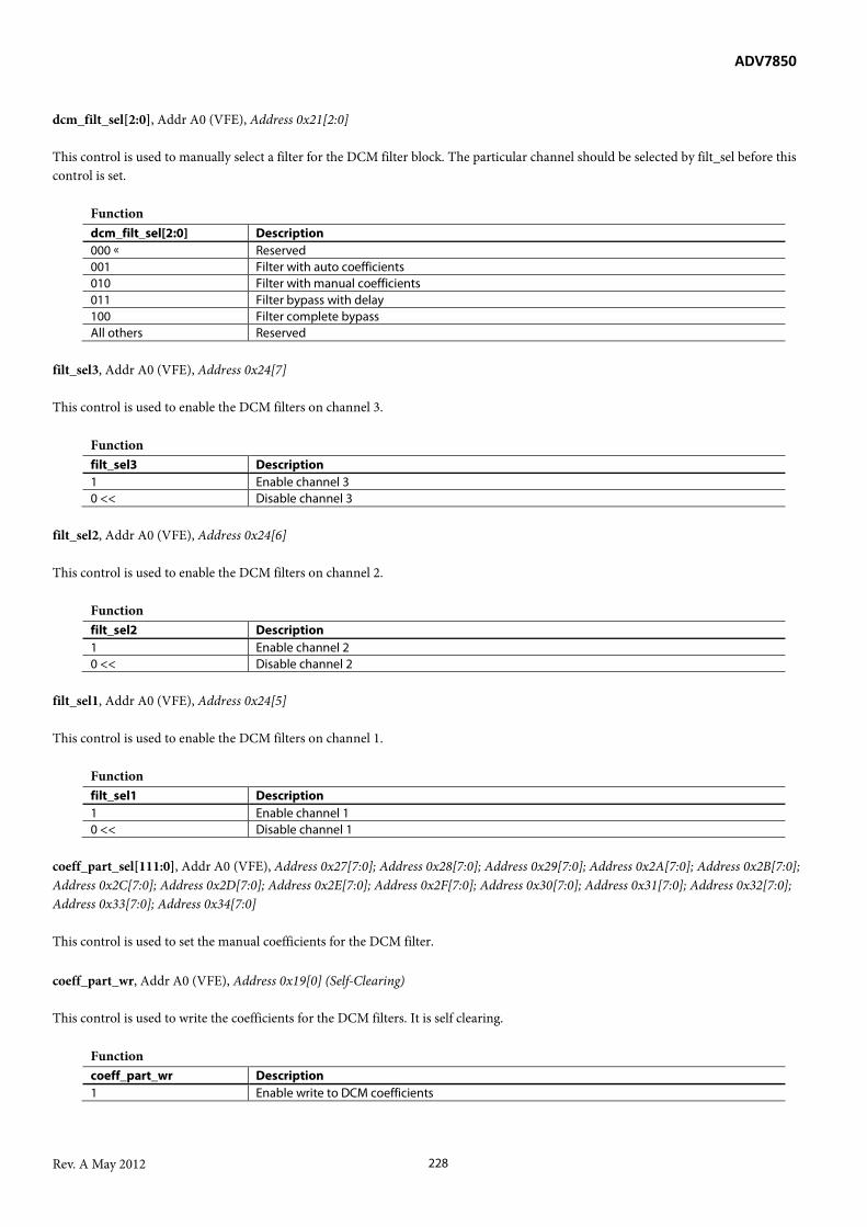
ADV7850
Rev. A May 2012 228
dcm_filt_sel[2:0], Addr A0 (VFE), Address 0x21[2:0] This control is used to manually select a filter for the DCM filter block. The particular channel should be selected by filt_sel before this control is set.
Function dcm_filt_sel[2:0] Description 000 Reserved 001 Filter with auto coefficients 010 Filter with manual coefficients 011 Filter bypass with delay 100 Filter complete bypass All others Reserved
filt_sel3, Addr A0 (VFE), Address 0x24[7] This control is used to enable the DCM filters on channel 3.
Function filt_sel3 Description 1 Enable channel 3 0 << Disable channel 3
filt_sel2, Addr A0 (VFE), Address 0x24[6] This control is used to enable the DCM filters on channel 2.
Function filt_sel2 Description 1 Enable channel 2 0 << Disable channel 2
filt_sel1, Addr A0 (VFE), Address 0x24[5] This control is used to enable the DCM filters on channel 1.
Function filt_sel1 Description 1 Enable channel 1 0 << Disable channel 1
coeff_part_sel[111:0], Addr A0 (VFE), Address 0x27[7:0]; Address 0x28[7:0]; Address 0x29[7:0]; Address 0x2A[7:0]; Address 0x2B[7:0]; Address 0x2C[7:0]; Address 0x2D[7:0]; Address 0x2E[7:0]; Address 0x2F[7:0]; Address 0x30[7:0]; Address 0x31[7:0]; Address 0x32[7:0]; Address 0x33[7:0]; Address 0x34[7:0] This control is used to set the manual coefficients for the DCM filter. coeff_part_wr, Addr A0 (VFE), Address 0x19[0] (Self-Clearing) This control is used to write the coefficients for the DCM filters. It is self clearing.
Function coeff_part_wr Description 1 Enable write to DCM coefficients
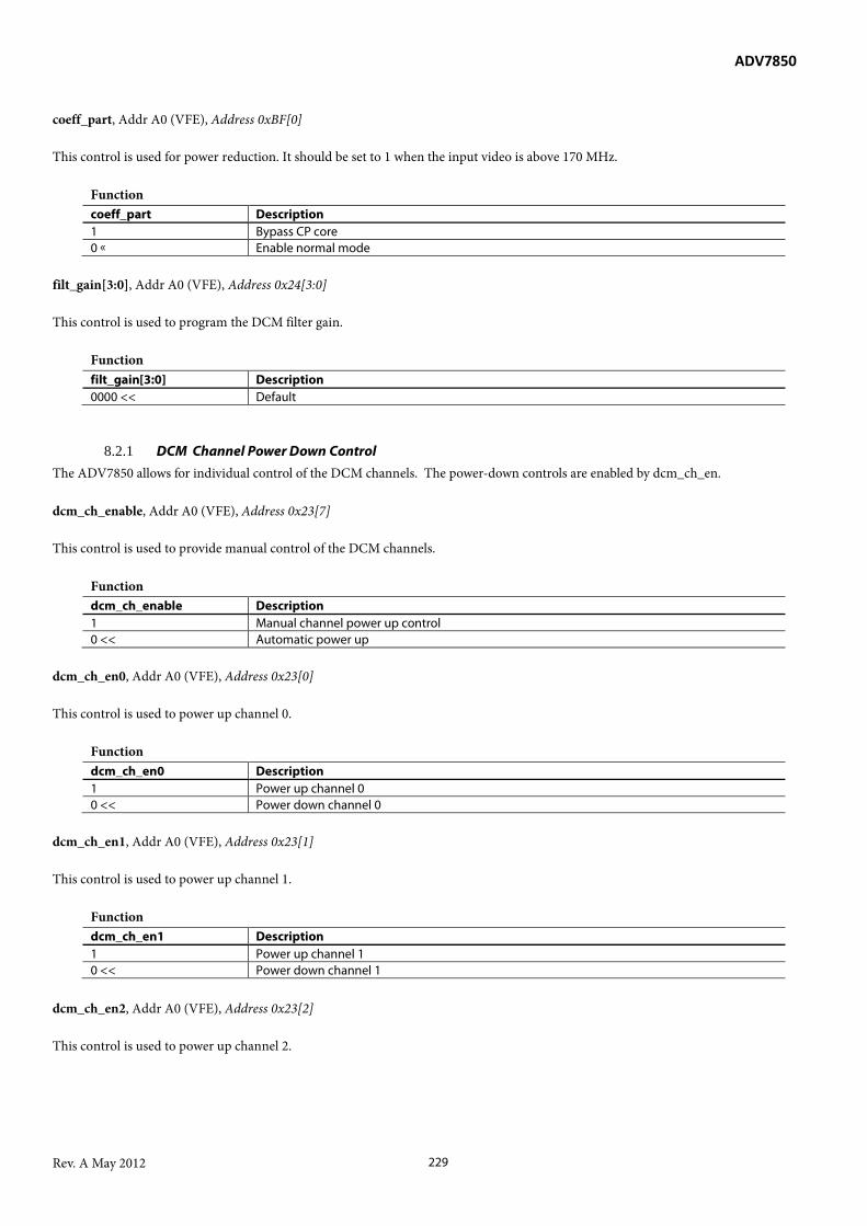
ADV7850
Rev. A May 2012 229
coeff_part, Addr A0 (VFE), Address 0xBF[0] This control is used for power reduction. It should be set to 1 when the input video is above 170 MHz.
Function coeff_part Description 1 Bypass CP core 0 Enable normal mode
filt_gain[3:0], Addr A0 (VFE), Address 0x24[3:0] This control is used to program the DCM filter gain.
Function filt_gain[3:0] Description 0000 << Default
8.2.1 DCM Channel Power Down Control The ADV7850 allows for individual control of the DCM channels. The power-down controls are enabled by dcm_ch_en. dcm_ch_enable, Addr A0 (VFE), Address 0x23[7] This control is used to provide manual control of the DCM channels.
Function dcm_ch_enable Description 1 Manual channel power up control 0 << Automatic power up
dcm_ch_en0, Addr A0 (VFE), Address 0x23[0] This control is used to power up channel 0.
Function dcm_ch_en0 Description 1 Power up channel 0 0 << Power down channel 0
dcm_ch_en1, Addr A0 (VFE), Address 0x23[1] This control is used to power up channel 1.
Function dcm_ch_en1 Description 1 Power up channel 1 0 << Power down channel 1
dcm_ch_en2, Addr A0 (VFE), Address 0x23[2] This control is used to power up channel 2.

ADV7850
Rev. A May 2012 230
Function dcm_ch_en2 Description 1 Power up channel 2 0 << Power down channel 2
dcm_ch_en3, Addr A0 (VFE), Address 0x23[3] This control is used to power up channel 3.
Function dcm_ch_en3 Description 1 Power up channel 3 0 << Power down channel 3
8.3 COLOR SPACE CONVERSION MATRIX The ADV7850 provides any-to-any color space conversion support. It supports formats such as RGB, YUV, and YCbCr. The Color Space Converter (CSC) is designed to run at speeds of up to 170 MHz. The CSC is in the CP block (CP CSC). The CP also provides color controls for brightness, contrast, saturation and hue adjustments. The CP CSC is the main color space converter. The CPP block also has an automatic non programmable CSC. The ADV7850 will automatically configure the fixed CSC for certain modes, depending on the input and output formats and the use of the color control feature. The configuration of the color space conversion using the CP CSC block and a description of the adjustable controls is provided in Figure 76.
Figure 76: Configuring CP CSC Block
8.3.1 CP CSC Selection man_cp_csc_en, Addr 44 (CP), Address 0x69[4] This control is used to manually enable the CP CSC. By default, the CP CSC is automatically enabled in the case where either a color space conversion or video adjustment (hue, saturation, contrast, or brightness) is determined to be required due to other I2C settings. If man_cp_csc_en is set to 1, the CP CSC is forced into the enabled state.
From DPPChannel A, B & C
CP Color SpaceConversion Matrix
(CP CSC)
CP Color Control
CP_BRIGHTNESSCP_SATURATIONCP_CONTRASTCP_HUE
To CP CoreChannel A, B & C
0000
1111
Manual CSC Mode
Automatic CSC Mode
RGB_OUTINP_COLOR_SPACEALT_GAMMA
CSC_SCALEA1-A4[12:0]B1-B4[12:0]C1-C4[12:0]
VID_ADJ_EN
CSC_COEFF_SEL

ADV7850
Rev. A May 2012 231
Function man_cp_csc_en Description 0 CP CSC automatically enabled if required 1 Manual override to force CP CSC to be enabled
8.3.2 Selecting Automatic or Manual CP CSC Conversion Mode The ADV7850 CP CSC provides two modes for the CSC configuration: automatic CSC mode and manual CSC mode. In automatic CSC mode, the user is required to program the input color space and the output color space for the correct operation of the CSC matrix. Manual CSC mode allows the user to program all the color space conversion by manually programming CSC coefficients. csc_coeff_sel[3:0], Addr 44 (CP), Address 0x68[7:4] This control is used to select the mode in which the CP CSC operates.
Function csc_coeff_sel[3:0] Description 0000 CP CSC configuration in manual mode 1111 CP CSC configured in automatic mode xxxx Reserved
The CSC configuration mode is automated in the ADV7850. Automatic or manual CSC mode can be selected by setting the csc_coeff_sel[3:0] bits. When csc_coeff_sel[3:0] is set to 0b1111, the CSC mode is automatically selected, based on the input color space and output color space required and set through the following registers:
• inp_color_space[3:0] • rgb_out • alt_gamma
8.3.3 Automatic Color Space Conversion Matrix In automatic mode, the CSC matrix, AGC target gain values, and offset values can be configured automatically via the following set of registers:
• inp_color_space[3:0] • rgb_out • alt_gamma • op_656_range_sel
inp_color_space[3:0], Addr A0 (VFE), Address 0x02[7:4] This control is used to set the color space of the input video. It is to be used in conjunction with alt_gamma and rgb_out to configure the color space converter. A value of 4'b1111 selects automatic setting of the input color space base on the primary mode and video standard settings. Settings 1000 to 1110 are undefined.
Function inp_color_space[3:0] Description 0000 Force RGB (range 16 to 235) input 0001 Force RGB (range 0 to 255) input 0010 Force YCrCb input (601 color space) (range 16 to 235) 0011 Force YCrCb input (709 color space) (range 16 to 235) 0100 Force XVYCC 601 0101 Force XVYCC 709 0110

ADV7850
Rev. A May 2012 232
Table 47: Automatic Input Color Space Selection prim_mode[3:0] vid_std[5:0] Input Color Space Input Range Comments 0001 ≤ 1001 YcrCb601 0:255 Analog SD/ED modes 0001 > 1001 YcrCb709 0:255 Analog HD modes 0010 xxxx RGB 0:255 Analog GR modes 0101 xxxx Dependant on AVI
InfoFrame 0:255 for YUV HDMI component modes Dependant on AVI InfoFrame for RGB
0110 xxxx Dependant on AVI InfoFrame
0:255 for YUV HDMI graphic modes Dependant on AVI InfoFrame for RGB
rgb_out, Addr A0 (VFE), Address 0x02[1] This control is used to select the output color space and the correct digital blank level and offsets on the RGB or YPrPb outputs. It is used in conjunction with inp_color_space[3:0] and alt_gamma to select the applied CSC.
Function rgb_out Description 0 YPbPr color space output 1 RGB color space output
alt_gamma, Addr A0 (VFE), Address 0x02[3] This control is used to select the type of YPbPr color space conversion. It is to be used in conjunction with inp_color_space[3:0] and rgb_out. If alt_gamma is set to 1 and rgb_out is set to 0, a color space conversion is applied to convert from 601 to 709 or 709 to 601. It is valid only if rgb_out is set to 0.
Function alt_gamma Description 0 No conversion 1 Apply YUV601 to YUV709 conversion if input is YUV601, apply YUV709 to YUV601 conversion
if input is YUV709
Table 48: Automatic CSC Selection
inp_color_space[3:0] (Input Color Space) rgb_out
CSC Mode Used (Output)
alt_gamma = 0 alt_gamma = 1
00 - RGB 0 YCbCr 601 YCbCr 709 1 RGB RGB
01 - (YCbCr /YUV 601) 0 YCbCr 601 YCbCr 709 1 RGB RGB
10 - (YCbCr /YUV 709) 0 YCbCr 709 YCbCr 601 1 RGB RGB
csc_coeff_sel_rb[3:0], Addr 44 (CP), Address 0xF4[7:4] (Read Only) This readback displays the CP CSC conversion when configured in automatic mode.

ADV7850
Rev. A May 2012 233
Function csc_coeff_sel_rb[3:0] Description 0000 CSC bypassed 0001 YPbPr 601 to RGB 0011 YPbPr 709 to RGB 0101 RGB to YPbPr 601 0111 RGB to YPbPr 709 1001 YPbPr 709 to YPbPr 601 1010 YPbPr 601 to YPbPr 709 1111 CSC in manual mode xxxx Reserved
Table 49: CSC Configuration for All CSC Modes Reported by csc_coeff_sel_rb
CSC Mode
csc_
scal
e[1:
0]
A1 A2 A3 A4 B1 B2 B3 B4 C1 C2 C3 C4
0b0000 CSC in bypass mode. In this mode the CSC effectively performs a color conversion based on the CSC coefficients set in registers csc_scale, A1, A2, A3, A4, B1, B2, B3, B4, C1, C2, C3, and C4.
0b0001 0b01 0x0800 0x1A6A 0x1D50 0x0423 0x0800 0x0AF8 0x0000 0x1A84 0x0800 0x0000 0x0DDB 0x1912
0b0011 0b01 0x0800 0x1C54 0x1E89 0x0291 0x0800 0x0C52 0x0000 0x19D7 0x0800 0x0000 0x0E87 0x18BC
0b0101 0b00 0x0964 0x04C9 0x01D3 0x0000 0x1927 0x082D 0x1EAC 0x0800 0x1A93 0x1D3F 0x082D 0x0800
0b0111 0b00 0x0B71 0x0368 0x0127 0x0000 0x1893 0x082D 0x1F3F 0x0800 0x19B2 0x1E21 0x082D 0x0800
0b1001 0b01 0x0800 0x0188 0x00CB 0x1ED7 0x0000 0x07DE 0x1F6C 0x005B 0x0000 0x1F1D 0x07EB 0x007B
0b1010 0b01 0x0800 0x1E56 0x1F14 0x014A 0x0000 0x0834 0x009A 0x1F9A 0x0000 0x00EB 0x0826 0x1F78
8.3.4 Manual Color Space Conversion Matrix The CP CSC matrix in the ADV7850 is a 3 x 3 matrix with full programmability of all coefficients in the matrix in manual mode. Each coefficient is 12-bits wide to ensure signal integrity is maintained in the CP CSC section. The CP CSC contains three identical processing channels, one of which is shown in Figure 77. The main inputs labeled In_A, In_B, and In_C can come from each ADC. Each input to the individual channels to the CP CSC is multiplied by a separate coefficient for each channel. In Figure 77, these coefficients are marked A1, A2 and A3. The variable labeled A4 is used as an offset control for channel A in the CSC. There is also a further CP CSC control, csc_scale[1:0], which can be used to accommodate coefficients that extend the supported range. The functional diagram for a single channel in the CP CSC, as shown in Figure 77, is repeated for the other two remaining channels B and C. The coefficients for these channels are called B1, B2, B3, B4, C1, C2, C3 and C4.
Figure 77: Single CSC Channel
The coefficients mentioned previously are detailed in Table 50 along with the default values for these coefficients.
In_A [11:0]
In_C [11:0]
X
A1[12:0]
X
A2[12:0]
X
A3[12:0]
+ + +
A4[12:0]
In_B [11:0]
X 2
CSC_scale
Out_A [11:0]1
0

ADV7850
Rev. A May 2012 234
Table 50: CSC Coefficients Control
CP Map Address Reset Value (Hex) Description A1[12:0] 0x57 [4:0], 0x58 [7:0] 0x800 Coefficient for channel A A2[12:0] 0x55 [1:0], 0x56 [7:0] 0x57 [7:5] 0x000 Coefficient for channel A A3[12:0] 0x54 [6:0], 0x55 [7:2] 0x000 Coefficient for channel A B1[12:0] 0x5E [4:0], 0x5F [7:0] 0x000 Coefficient for channel B B2[12:0] 0x5C [1:0], 0x5D [7:0] 0x5E [7:5] 0x800 Coefficient for channel B B3[12:0] 0x5B [6:0], 0x5C [7:2] 0x000 Coefficient for channel B C1[12:0] 0x65 [4:0], 0x66 [7:0] 0x000 Coefficient for channel C C2[12:0] 0x63 [1:0], 0x64 [7:0] 0x65 [7:5] 0x000 Coefficient for channel C C3[12:0] 0x62 [6:0], 0x63 [7:2] 0x800 Coefficient for channel C csc_scale[1:0] 0x52 [7:6] 0x01 Scaling for CSC formula A4[12:0] 0x52 [4:0], 0x53 [7:0] 0x000 Offset for channel A B4[12:0] 0x59 [4:0], 0x5A [7:0] 0x000 Offset for channel B C4[12:0] 0x60[4:0], 0x61 [7:0] 0x000 Offset for channel C
csc_scale[1:0], Addr 44 (CP), Address 0x52[7:6] This control is used to set the CSC coefficient scalar.
Function csc_scale[1:0] Description 00 CSC scalar set to 1 01 CSC scalar set to 2 10 Reserved 11 Reserved
rb_csc_scale[1:0], Addr 44 (CP), Address 0x0B[7:6] (Read Only) This readback displays the CSC scale applied to CSC coefficients.
Function rb_csc_scale[1:0] Description xx Readback value
rb_a1[12:0], Addr 44 (CP), Address 0x10[4:0]; Address 0x11[7:0] (Read Only) This readback displays the CSC coefficient A1 modified by the video adjustment block.
Function rb_a1[12:0] Description xxxxxxxxxxxxx Readback value
rb_a2[12:0], Addr 44 (CP), Address 0x0E[1:0]; Address 0x0F[7:0]; Address 0x10[7:5] (Read Only) This readback displays the CSC coefficient A2 modified by the video adjustment block.
Function rb_a2[12:0] Description xxxxxxxxxxxxx Readback value
rb_a3[12:0], Addr 44 (CP), Address 0x0D[6:0]; Address 0x0E[7:2] (Read Only) This readback displays the CSC coefficient A3 modified by the video adjustment block.

ADV7850
Rev. A May 2012 235
Function rb_a3[12:0] Description xxxxxxxxxxxxx Readback value
rb_a4[12:0], Addr 44 (CP), Address 0x0B[4:0]; Address 0x0C[7:0] (Read Only) This readback displays the CSC coefficient A4 modified by the video adjustment block.
Function rb_a4[12:0] Description xxxxxxxxxxxxx Readback value
rb_b1[12:0], Addr 44 (CP), Address 0x17[4:0]; Address 0x18[7:0] (Read Only) This readback displays the CSC coefficient B1 modified by the video adjustment block.
Function rb_b1[12:0] Description xxxxxxxxxxxxx Readback value
rb_b2[12:0], Addr 44 (CP), Address 0x15[1:0]; Address 0x16[7:0]; Address 0x17[7:5] (Read Only) This readback displays the CSC coefficient B2 modified by the video adjustment block.
Function rb_b2[12:0] Description xxxxxxxxxxxxx Readback value
rb_b3[12:0], Addr 44 (CP), Address 0x14[6:0]; Address 0x15[7:2] (Read Only) This readback displays the CSC coefficient B3 modified by the video adjustment block.
Function rb_b3[12:0] Description xxxxxxxxxxxxx Readback value
rb_b4[12:0], Addr 44 (CP), Address 0x12[4:0]; Address 0x13[7:0] (Read Only) This readback displays the CSC coefficient B4 modified by the video adjustment block.
Function rb_b4[12:0] Description xxxxxxxxxxxxx Readback value
rb_c1[12:0], Addr 44 (CP), Address 0x1E[4:0]; Address 0x1F[7:0] (Read Only) This readback displays the CSC coefficient C1 modified by the video adjustment block.
Function rb_c1[12:0] Description xxxxxxxxxxxxx Readback value
rb_c2[12:0], Addr 44 (CP), Address 0x1C[1:0]; Address 0x1D[7:0]; Address 0x1E[7:5] (Read Only) This readback displays the CSC coefficient C2 modified by the video adjustment block.
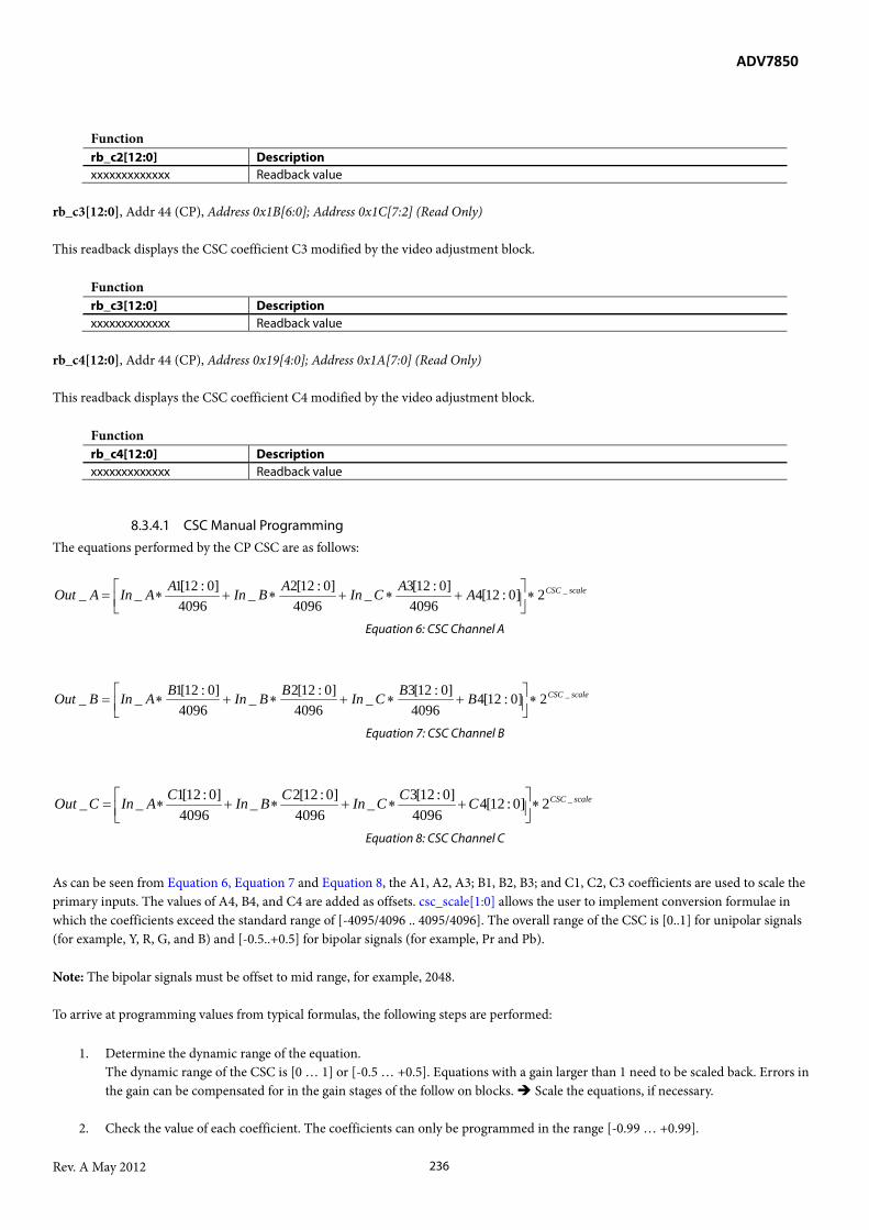
ADV7850
Rev. A May 2012 236
Function rb_c2[12:0] Description xxxxxxxxxxxxx Readback value
rb_c3[12:0], Addr 44 (CP), Address 0x1B[6:0]; Address 0x1C[7:2] (Read Only) This readback displays the CSC coefficient C3 modified by the video adjustment block.
Function rb_c3[12:0] Description xxxxxxxxxxxxx Readback value
rb_c4[12:0], Addr 44 (CP), Address 0x19[4:0]; Address 0x1A[7:0] (Read Only) This readback displays the CSC coefficient C4 modified by the video adjustment block.
Function rb_c4[12:0] Description xxxxxxxxxxxxx Readback value
8.3.4.1 CSC Manual Programming The equations performed by the CP CSC are as follows:
Equation 6: CSC Channel A
Equation 7: CSC Channel B
Equation 8: CSC Channel C
As can be seen from Equation 6, Equation 7 and Equation 8, the A1, A2, A3; B1, B2, B3; and C1, C2, C3 coefficients are used to scale the primary inputs. The values of A4, B4, and C4 are added as offsets. csc_scale[1:0] allows the user to implement conversion formulae in which the coefficients exceed the standard range of [-4095/4096 .. 4095/4096]. The overall range of the CSC is [0..1] for unipolar signals (for example, Y, R, G, and B) and [-0.5..+0.5] for bipolar signals (for example, Pr and Pb). Note: The bipolar signals must be offset to mid range, for example, 2048. To arrive at programming values from typical formulas, the following steps are performed:
1. Determine the dynamic range of the equation. The dynamic range of the CSC is [0 … 1] or [-0.5 … +0.5]. Equations with a gain larger than 1 need to be scaled back. Errors in the gain can be compensated for in the gain stages of the follow on blocks. Scale the equations, if necessary.
2. Check the value of each coefficient. The coefficients can only be programmed in the range [-0.99 … +0.99].
scaleCSCAACInABInAAInAOut _2]0:12[44096
]0:12[3_4096
]0:12[2_4096
]0:12[1__ ∗
+∗+∗+∗=
scaleCSCBBCInBBInBAInBOut _2]0:12[44096
]0:12[3_4096
]0:12[2_4096
]0:12[1__ ∗
+∗+∗+∗=
scaleCSCCCCInCBInCAInCOut _2]0:12[44096
]0:12[3_4096
]0:12[2_4096
]0:12[1__ ∗
+∗+∗+∗=

ADV7850
Rev. A May 2012 237
3. To support larger coefficients, the csc_scale[1:0] function should be used.
4. Determine the setting for csc_scale[1:0] and adjust coefficients, if necessary.
5. Program the coefficient values. Convert the float point coefficients into 12-bit fixed decimal format. Convert into binary format,
using twos complement for negative values. Program A1 .. A3, B1 .. B3, C1 .. C3.
6. Program the offset values. Depending on the type of CSC, offsets may have to be used. Program A4, B4, C4.
8.3.4.2 CSC Example
The following set of equations gives an example of a conversion from a gamma corrected RGB signal into a YCbCr color space signal.
Note: The original equations give offset values of 128 for the Pr and Pb components. The value of 128 equates to half the range on an 8-bit system. It must be noted that the CSC operates on a 12-bit range. The offsets, therefore, must be changed from 128 to half the range of a 12-bit system, which equates to 2048. The maximum range for each equation, that is, each output data path, can only be [0 ... 1] or [-0.5 ... +0.5]. Equations with a larger gain must be scaled back into range. The gain error can be compensated for in the gain stage of the follow on blocks. The ranges of the three equations are:
Equation Minimum Value Maximum Value Range Y 0 + 0 + 0 = 0 0.59 + 0.3 + 0.11 = 1 [0 … 1] = 1 Pb (-0.34) + (-0.17) = -0.51 0.51 [-0.51 … 0.51] = 1.02 Pr (-0.43) + (-0.08) = -0.51 0.51 [-0.51 … 0.51] = 1.02
As can be seen from this table, the range for the Y component fits into the CSC operating range. However, the Pb and Pr ranges slightly exceed the range. To bring all equations back into the supported range, they should be scaled back by 1/1.02. If equations fall outside the supported range, overflow or underflow can occur and undesirable wrap around effects (large number overflowing to small ones) can happen.
Note: The scaling of the dynamic range does not affect the static offset.
scaleCSCAACInABInAAInAOut _2]0:12[44096
]0:12[3_4096
]0:12[2_4096
]0:12[1__ ∗
+∗+∗+∗=
scaleCSCBBCInBBInBAInBOut _2]0:12[44096
]0:12[3_4096
]0:12[2_4096
]0:12[1__ ∗
+∗+∗+∗=
scaleCSCCCCInCBInCAInCOut _2]0:12[44096
]0:12[3_4096
]0:12[2_4096
]0:12[1__ ∗
+∗+∗+∗=
BRGBRGY ∗+∗+∗=∗+∗+∗= 11.029.058.002.111.0
02.13.0
02.159.0
20485.017.033.0204802.151.0
02.117.0
02.134.0
+∗+∗−∗−=+∗+∗−
+∗−
= BRGBRGPb
204808.05.042.0204802.108.0
02.151.0
02.143.0Pr +∗−∗+∗−=+∗
−+∗+∗
−= BRGBRG

ADV7850
Rev. A May 2012 238
Check the value of each coefficient: The maximum value for each coefficient on its own can only be within the range of -4095/4096 to 4095/4096, which equals [-0.999755859375 .. 0.999755859375]. Values outside this range do not fit into the 12-bit fixed point format used to program the coefficients. If the value of one or more coefficients after scaling of the overall equation exceeds the supported coefficient range, csc_scale[1:0] should be set. With csc_scale[1:0] set high, all coefficients must be scaled by half, which makes them fit into the given coefficient range. The overall outputs of the CSC are gained up by a fixed value of two, thus compensating for the scaled down coefficients. In the above example:
Each coefficient on its own is within the range of .
Therefore, all coefficients can be programmed directly and csc_scale[1:0] should be set to 0. Notes:
• To achieve a coefficient value of 1.0 for any given coefficient, csc_scale should be set high and the coefficient should actually be programmed to a value of 0.5. Otherwise, the largest value would be 4095/4096 = 0.9997, which is not exactly 1. While this value could be interpreted as a 1, it is recommended to use the value of 0.5 and csc_scale for maximum accuracy.
• For very large coefficient values, for example, 2.58, a combination of csc_scale[1:0] and equation scaling should be used.
• Set csc_scale high (2.58/2 = 1.29) and scale the overall equation by slightly more than 1.28 (coefficient falls within the supported range of [-0.999 … +0.999]).
8.3.5 CSC in Pass-through Mode It is possible to configure the CP CSC in a pass-through mode. In this mode, the CP CSC is used but does not alter the data it processes. The CP CSC pass-through mode is obtained using the following settings:
• Set man_cp_csc_en to 1’b1 • Set csc_coeff_sel[3:0] to 4’b0000 • Leave the following registers from the CP Map at the default:
CSC_SCALE = 1 (default value) A4 = A3 = A2 = 0x000 (default value) B4 = B3 = B1 = 0x000 (default value) C4 = C2 = C1 = 0x000 (default value) A1 = B2 = C3 = 0x800 (default value)
Note: The DPP CSC is always in pass-through mode unless the ADV7850 is processing an RGB input, outputting this input in the RGB color space and vid_adj_en is enabled.
8.4 COLOR CONTROLS The ADV7850 has a color control feature that can adjust the brightness, contrast, saturation, and hue properties. vid_adj_en, Addr 44 (CP), Address 0x3E[7] This control is used to enable video adjustment. It is used to select whether or not the color controls feature is enabled. The color controls feature is configured via the parameters cp_contrast[7:0], cp_saturation[7:0], cp_brightness[7:0] and cp_hue[7:0]. The CP CSC must also be enabled for the color controls to be effective.
40964095
40964095
≤≤− Coeff

ADV7850
Rev. A May 2012 239
Function vid_adj_en Description 0 Disable color controls 1 Enable color controls
cp_contrast[7:0], Addr 44 (CP), Address 0x3A[7:0] This control is used to set the contrast. It is an unsigned value represented in a 1.7 binary format. The MSB represents the integer part of the contrast value, which is either 0 or 1. The seven LSBs represents the fractional part of the contrast value. The fractional part has the range [0 to 0.99]. This control is functional if vid_adj_en is set to 1.
Function cp_contrast[7:0] Description 00000000 Contrast set to minimum 10000000 Default 11111111 Contrast set to maximum
cp_saturation[7:0], Addr 44 (CP), Address 0x3B[7:0] This control is used to set the saturation. It is an unsigned value represented in a 1.7 binary format. The MSB represents the integer part of the saturation value, which is either 0 or 1. The seven LSBs represent the fractional part of the saturation value. The fractional part has a [0 to 0.99] range. This control is functional if vid_adj_en is set to 1.
Function cp_saturation[7:0] Description 00000000 Saturation set to minimum 10000000 Default 11111111 Saturation set to maximum
cp_brightness[7:0], Addr 44 (CP), Address 0x3C[7:0] This control is used to set the brightness. It is a signed value. The effective brightness value applied to the luma is obtained by multiplying the programmed value cp_brightness with a gain of 4. The brightness applied to the luma has a range of [-512 to 508]. This control is functional if vid_adj_en is set to 1.
Function cp_brightness[7:0] Description 00000000 Offset applied to luma is 0. 01111111 Offset applied to luma is 508d. This value corresponds to brightest setting. 11111111 Offset applied to luma is -512d. This value corresponds to darkest setting.
cp_hue[7:0], Addr 44 (CP), Address 0x3D[7:0] This control is used to set the hue. This control represents an unsigned value which provides hue adjustment. The effective hue applied to the chroma is [(cp_hue[7:0] * 180)/256 - 90]. The range of the effective hue applied to the chroma is [-90° to 90°].
Function cp_hue[7:0] Description 00000000 Hue of -90° applied to chroma 00001111 Hue of 0° applied to chroma 11111111 Hue of 90° applied to chroma
The effective hue applied to the Chroma is given by Equation 9. The range of the effective hue applied to the chroma is [-90º to 90º].

ADV7850
Rev. A May 2012 240
90256]0:7[_180
−⋅
=huecpHUE
Equation 9: Hue in Degree Unit Applied to Chroma via cp_hue[7:0] Control

ADV7850
Rev. A May 2012 241
9 COMPONENT PROCESSOR
Figure 78: Component Processor Block Diagram
9.1 INTRODUCTION TO COMPONENT PROCESSOR A simplified block diagram of the CP on the ADV7850 is shown in Figure 78. Data is supplied to the CP from the Data Preprocessor (DPP). The CP circuitry is activated under the control of prim_mode[3:0] and vid_std[5:0]. The CP is activated for the following modes of operation:
• GR modes: PC graphic-based signals in RGB format • HD modes: high definition video signals in YPbPr/RGB format • PR mode: progressive scan video signals in YPbPr/RGB format, for example, 525p and 625p • SD modes: component standard definition in YPbPr/RGB format, for example, 525i and 625i
The CP performs the following functions:
• Digital fine clamping of the video signal • Manual and automatic gain control • Manual offset correction • Saturation
The CP has the following capabilities:
• Generates HSync, VSync, FIELD, and Data Enable (DE) timing reference for the HDMI Tx section • Detects the source from which the video is to be synchronized • Measures noise and calibration levels • Measures the depth of the horizontal synchronization pulse used for AGC • Detects the presence of Macrovision encoded signals • Color space conversion • Color control adjustment
DelayDig ita l
Fin eClam p
GainCo n tro l
C o m pon e n tP ro cess o r
Offs etAd d er
No is e andCalib ra tio n
Activ e Pe a k andH Syn c Dep th
M V & C G M SDete ctio n
Syn c So u rc e an dPo larity
D ete ctio n(S S PD )
Stan d ardId en tific atio n
(ST D I)
Syn c Extra cto r
Vid eo DataC H A , C H B and
C H C In p ut
H S /VS /FOutput toHDMI Tx Section
Video DataC H A, C H B andC H C Output toHDMI Tx Section
Measurem entBlock (=> I2C )Video DataProcess ingBlock
C P C SC
Syn c So u rc e an dPo larity
D ete ctio n(S S PD )
Stan d ardId en tific atio n
(ST D I)
S y n c P ro cess in gC h a nn e l 1
S y n c P ro cess in gC h a nn e l 2

ADV7850
Rev. A May 2012 242
9.2 CLAMP OPERATION For analog signals that enter the CP block, there are two clamp methods applied to the video signal:
• An analog voltage clamp block prior to the ADCs • A digital fine clamp that operates after the DPP block
The analog voltage clamp signal operates on the input video prior to digitization. Figure 79 shows the position within the active video lines where the voltage clamp switches on. The position of the window is changed automatically (depending on prim_mode[3:0] and vid_std[5:0]) to suit the video standard in question.
Figure 79: Position of Voltage Clamp Window The CP contains a digital fine clamp block. Its main purposes are:
• To compensate for variations of the voltage clamps in the analog domain • To allow a clamp to operate even if the input signal is coming from a digital source, for example, external ADC
The digital fine clamp operates in three separate feedback loops, one for each channel. The incoming video signal level is measured at the back porch. The level error, that is, clamp error, is compensated for by subtracting or adding a digital number to the datastream. The digital clamp loop can be operated in an automatic or a manual mode with the following options:
• The clamp values for channels B and C can be set manually. This is the recommended mode. • The clamp value is determined automatically on a line-by-line basis. • The clamp loops can be frozen. This means that the currently active offsets will no longer be updated but will be applied
permanently. • The clamp value for channel A can be set manually (static value).
Note: The target clamp level for black input is a digital code of 0. This is to facilitate the highest possible signal to noise ratio (SNR). Some interfaces, for example, ITU-R. BT656, require black to correspond to a value other than 0. To facilitate this, there is an additional independent offset adder block after the gain multipliers for which separate fixed offset values can be supplied. Refer to Section 9.4 for additional information. clmp_freeze Freeze Digital Clamp, CP Map, Address 0x6C, [5] The clmp_freeze bit stops the three digital fine clamp loops for channels A, B, and C from updating. The currently active clamp values are applied continuously. All three loops are affected together; it is not possible to freeze the clamps for the channels individually. clmp_freeze, Addr 44 (CP), Address 0x6C[5] This control is used to stop the digital fine clamp loops for channels A, B and C from updating.
Function clmp_freeze Description 0 Clamp value updated on every active video line 1 Clamp loops stopped and not updated
To facilitate an external clamp loop for channel A, the internal clamp value determined by the digital fine clamp block can be overridden by a manual value programmed in the I2C. The two corresponding control values are clmp_a_man and clmp_a[11:0].
Analog Video Input
Voltage Clamp Control Signal
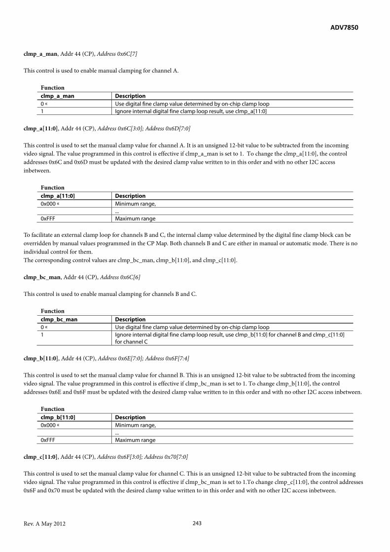
ADV7850
Rev. A May 2012 243
clmp_a_man, Addr 44 (CP), Address 0x6C[7] This control is used to enable manual clamping for channel A.
Function clmp_a_man Description 0 Use digital fine clamp value determined by on-chip clamp loop 1 Ignore internal digital fine clamp loop result, use clmp_a[11:0]
clmp_a[11:0], Addr 44 (CP), Address 0x6C[3:0]; Address 0x6D[7:0] This control is used to set the manual clamp value for channel A. It is an unsigned 12-bit value to be subtracted from the incoming video signal. The value programmed in this control is effective if clmp_a_man is set to 1. To change the clmp_a[11:0], the control addresses 0x6C and 0x6D must be updated with the desired clamp value written to in this order and with no other I2C access inbetween.
Function clmp_a[11:0] Description 0x000 Minimum range, ... 0xFFF Maximum range
To facilitate an external clamp loop for channels B and C, the internal clamp value determined by the digital fine clamp block can be overridden by manual values programmed in the CP Map. Both channels B and C are either in manual or automatic mode. There is no individual control for them. The corresponding control values are clmp_bc_man, clmp_b[11:0], and clmp_c[11:0]. clmp_bc_man, Addr 44 (CP), Address 0x6C[6] This control is used to enable manual clamping for channels B and C.
Function clmp_bc_man Description 0 Use digital fine clamp value determined by on-chip clamp loop 1 Ignore internal digital fine clamp loop result, use clmp_b[11:0] for channel B and clmp_c[11:0]
for channel C clmp_b[11:0], Addr 44 (CP), Address 0x6E[7:0]; Address 0x6F[7:4] This control is used to set the manual clamp value for channel B. This is an unsigned 12-bit value to be subtracted from the incoming video signal. The value programmed in this control is effective if clmp_bc_man is set to 1. To change clmp_b[11:0], the control addresses 0x6E and 0x6F must be updated with the desired clamp value written to in this order and with no other I2C access inbetween.
Function clmp_b[11:0] Description 0x000 Minimum range, ... 0xFFF Maximum range
clmp_c[11:0], Addr 44 (CP), Address 0x6F[3:0]; Address 0x70[7:0] This control is used to set the manual clamp value for channel C. This is an unsigned 12-bit value to be subtracted from the incoming video signal. The value programmed in this control is effective if clmp_bc_man is set to 1.To change clmp_c[11:0], the control addresses 0x6F and 0x70 must be updated with the desired clamp value written to in this order and with no other I2C access inbetween.

ADV7850
Rev. A May 2012 244
Function clmp_c[11:0] Description 0x000 Minimum range, ... 0xFFF Maximum range
clamp_avg_fctr The ADV7850 provides a special filter option for the auto clamp mode. The purpose of this filter is to provide a smoothening mechanism when the clamping value for each channel is being changed continuously in significant amounts by the autoclamping mechanism. The filter is an IIR filter with an effective function of:
YN = (1-A) * YN-1 + A * XN where A is the filter coefficient. The value of A can vary from 1 to 1/32 lines. A value of 1 indicates no filtering of the clamp and is a pass through option for the autoclamp value. clamp_avg_fctr[1:0], Addr 44 (CP), Address 0xC5[7:6] This control is used to set the coefficient A of the IIR filter used for autoclamp mode. The function transfer is Y[N]=(1-A)*Y[N-1]+A*X[N].
Function clamp_avg_fctr[1:0] Description 00 No filtering, A=1 01 Clamp is averaged over 8 lines, A=1/8 10 Clamp is averaged over 16 lines, A=1/16 11 Clamp is averaged over 32 lines, A=1/32
9.3 CP GAIN OPERATION The digital gain block of the CP consists of three multipliers in the data paths of channel A, B, and C, as well as one single automatic gain control loop. The gain control can be operated in manual or automatic mode.
9.3.1 Features of Manual Gain Control The gain values for the three channels can be programmed separately via I2C registers. This is the recommended mode.
9.3.2 Features of Automatic Gain Control The gain value is determined automatically, based on a signal with an embedded horizontal synchronization pulse on channel A. The automatic gain control loop can be frozen, for example, after settling. The gain value for analog inputs with separate HSync and VSync timing signals, and HDMI receiver inputs are controlled via the op_656_range bit.
9.3.3 Manual Gain and Automatic Gain Control Selection Figure 80 shows how the gain is applied to the video data processes by the CP section. The following gain configurations are available:
• Gain Configuration Dependant on the Output Range This configuration is enabled by setting agc_mode_man to 0 and by setting the part in SDP, COMP or GR mode via prim_mode and vid_std. In this case the gain applied to the video data processed by the CP core is determined by the control bit op_656_range.

ADV7850
Rev. A May 2012 245
• Manual Gain Configuration This configuration is enabled by setting agc_mode_man to 1 and gain_man to 1. In this case the gain applied to the video data processed by the CP core is configured via the control registers a_gain[9:0], b_gain[9:0] and c_gain[9:0].
• Automatic Gain Control Configuration
This configuration is enabled by setting agc_mode_man to 1 and gain_man to 0. The detection block, Synchronization Source and Polarity Detector (SSPD), is used to determine automatically the presence of external digital synchronizations, for example, HSync/VSync, or embedded synchronization. The detection result of the SSPD block is used to enable/disable the automatic gain control mode. If SSPD detects the presence of external (that is, digital) synchronization signals, the gain block in the CP core is controlled by op_656_range because it is assumed that there is no embedded synchronization present and it is, therefore, not possible to adjust the gain automatically.
• If the SSPD does not find any external synchronization signal, it concludes that the synchronization must be embedded. This switches the gain block in the CP core into automatic mode (refer to Section 9.7). This function can be disabled using the AGC mode manual enable control, agc_mode_man, as illustrated in Figure 80.
Figure 80: CP Automatic Gain Controls agc_mode_man, Addr 44 (CP), Address 0x73[6] This control is used to set how the gain for all three channels is configured.
Function agc_mode_man Description 0 Gain dependant on type of input and op_656_range 1 Gain operation controlled by gain_man
9.3.4 Manual Gain Control The automatic gain control (AGC) can be completely disabled by setting the gain control block into a manual mode. By setting the gain_man bit, the gain factors for channels A, B, and C are no longer taken from the AGC, but are replaced by three dedicated I2C registers. Using these factors with the hsd_fb[9:0] register, it is possible to implement an off-chip AGC if desired. The range for the gain is [0…3.999]. The registers a_gain[9:0], b_gain[9:0], and c_gain are in 2.8 binary format and can be set as shown in Equation 10.
( )256]0:9[_ ×= GAINfloorgainx where:
40 <≤ GAIN
AGC_MODE_MANNo Yes
OP_656_RANGE GAIN
0 (0-255 Output) (255-0+1)x16/1344 = 3.047
(235-16+1)x16/1344 = 2.6171 (16-235 Y/RGB,16-240 CrCb)
SSPD detectedembedded syncs?
GAIN_MAN
AGCActive
Set gain based onA/B/C_GAIN[9:0]
values
OP_656_RANGE GAIN
0 (0-255 Output) (255-0+1)x16/1344 = 3.047
(235-16+1)x16/1344 = 2.6171 (16-235 Y/RGB,16-240 CrCb)
Yes No
Yes No

ADV7850
Rev. A May 2012 246
( )floor is the floor function that returns the largest integer not greater than its input parameter X refers to A, B, and C
Equation 10: CP Manual Gain
Example:
Example Gaindec a_gain[9:0] 0.5 0x80 0.98887 0xFD 2.5 0x280
gain_man, Addr 44 (CP), Address 0x73[7] This control is used to enable the gain factor to be set by the AGC or manually.
Function gain_man Description 0 AGC controls gain for all three channels 1 Manual gains used for all three channels
a_gain[9:0], Addr 44 (CP), Address 0x73[5:0]; Address 0x74[7:4] This control is used to set the manual gain value for channel A. It is an unsigned value in a 2.8 binary format. To change it, the control at addresses 0x73 and 0x74 must be written to in this order with no I2C access inbetween.
Function a_gain[9:0] Description 0x000 Gain of 0 0x100 Unity gain 0x3FF Gain of 3.99
b_gain[9:0], Addr 44 (CP), Address 0x74[3:0]; Address 0x75[7:2] This control is used to set the manual gain value for channel B. It stores an unsigned value in a 2.8 binary format. To change it, the control at addresses 0x74 and 0x75 must be written to in this order with no I2C access inbetween.
Function b_gain[9:0] Description 0x000 Gain of 0 0x100 Unity gain 0x3FF Gain of 3.99
c_gain[9:0], Addr 44 (CP), Address 0x75[1:0]; Address 0x76[7:0] This control is used to set the manual gain value for channel C. It stores an unsigned value in a 2.8 binary format. To change it, the control at addresses 0x75 and 0x76 must be written to in this order with no I2C access inbetween.
Function c_gain[9:0] Description 0x000 Gain of 0 0x100 Unity gain 0x3FF Gain of 3.99

ADV7850
Rev. A May 2012 247
9.3.5 Manual Gain Filter Mode The ADV7850 provides a special filter option for the manual gain mode. This is functional only when manual gain is enabled. The purpose of this filter is to be a smoothing mechanism when the manual gain value is updated continuously by an external system based on either external or readback conditions in the ADV7850. The filter designed is an IIR filter with a transfer function of the form:
YN = (1-A)*YN-1 + A*XN where A is the filter coefficient.
The values possible for A can vary from 1 (no filtering) to 1/128K (K = 1024). The value of coefficient A is chosen by programming cp_gain_filt[3:0]. cp_gain_filt[3:0], Addr 44 (CP), Address 0x84[7:4] This control is used to set the coefficient A of the IIF filter to filter the gain applied to the video signal when the gain is set manually. The value set in this control is effective only when manual gain is enabled. The filter is designed as an IIR filter with a transfer function of the form Y[N]=(1-A)*y[N-1]+A*X[N].
Function cp_gain_filt[3:0] Description 0000 No filtering, i.e. coefficient A = 1 0001 Coefficient A = 1/128 lines 0010 Coefficient A = 1/256 lines 0011 Coefficient A = 1/512 lines 0100 Coefficient A = 1/1024 lines 0101 Coefficient A = 1/2048 lines 0110 Coefficient A = 1/4096 line
9.3.6 Automatic Gain Control The AGC of the CP takes measurements of the signal on channel A and determines an appropriate gain value for all three channels. For the block to operate, it is necessary that a signal with an embedded synchronization pulse is fed through to channel A, for example, Y or G. The AGC measures the depth of this synchronization pulse and compares it against a target value. The hsd_cha[9:0] readback register is used to determine if there is a synchronization pulse on the data. If no synchronization pulse is found, AGC cannot work and the manual gain control should be enabled. The target value for the AGC can come from three sources. There are two predefined values of 300 mV and 286 mV (the hs_norm bit is used to decide between the two values) and there is the option of setting an arbitrary target value by setting agc_tar_man, which enables the usage, and agc_tar[9:0], which sets the arbitrary target level. In some applications, it is desirable to use the AGC to gain the signal to a smaller range, use the Offset block to preserve the synchronizations (by lifting the entire video signal up), and thus output the full digitized waveform (including synchronizations) within the 12-bit output range. For this application, the agc_tar[9:0] value is very important. For more information, refer to Section 9.4.
Equation 11: CP AGC Target Value
Note: The 12-bit target code for white is nominally 940, the target code for black is 64. Examples:
dec mV HSync mV
mV tar agc
375 700 300 ) 64 940 ( _ 300 = • − = =
dec mV HSync mV mV tar agc 351
714 286 ) 64 940 ( _ 286 = • − = =
mV mV
Black White t VideoHeigh SyncHeight Code Code tar agc • − = ) ( ] 0 : 9 [ _

ADV7850
Rev. A May 2012 248
An error signal is derived from the comparison of the measured synchronization depth and the target value. The error signal is weighted by a factor that allows different response times to be selected (agc_tim[2:0] is used to select different time constants). The resulting gain value is applied to all three channels A, B, and C. agc_freeze allows the AGC loop to be stopped, that is, frozen. If frozen, the currently active gain is no longer updated but is applied continuously to all three datastreams. hs_norm, Addr 44 (CP), Address 0x71[3] This control is used to select the nominal HSync depth.
Function hs_norm Description 0 AGC target scales video as per 300 mV horizontal synchronization depth 1 AGC target scales video as per 286 mV horizontal synchronization depth
agc_tar_man, Addr 44 (CP), Address 0x71[5] This control is used to enable the manual target level.
Function agc_tar_man Description 0 AGC operates based on 300 mV or 286 mV horizontal synchronization depth, use hs_norm to
select 1 AGC operates based on agc_tar[9:0]
agc_tar[9:0], Addr 44 (CP), Address 0x71[7:6]; Address 0x72[7:0] This control is used to enable the manual AGC target value. It is used to set the target value for the horizontal synchronization depth after gain is applied. It is an unsigned value.
Function agc_tar[9:0] Description 0x000 Minimum range, … 0x3FF Maximum range
agc_freeze, Addr 44 (CP), Address 0x71[4] This control is used to enable AGC freeze.
Function agc_freeze Description 0 AGC loop operational. 1 AGC loop frozen and not updated further. Last gain value becomes static.
agc_tim[2:0], Addr 44 (CP), Address 0x71[2:0] This control is used to select the AGC time constant.

ADV7850
Rev. A May 2012 249
Function agc_tim[2:0] Description 000 100 lines 001 1 frame 010 0.5 sec 011 1 sec 100 2 sec 101 3 sec 110 5 sec 111 7 sec
9.3.6.1 Readback Signals from AGC Block The following readback signals are provided:
• Presently used gain value can be read back through cp_agc_gain[9:0] • Depth of the synchronization pulse on channel A (before gaining) through hsd_cha[9:0] • Depth of the synchronization pulse on channel A (after gaining) through hsd_fb[11:0] • Depth of the synchronization pulse on channel B (before gaining) through hsd_chb[9:0] • Depth of the synchronization pulse on channel C (before gaining) through hsd_chc[9:0]
Notes:
• hsd_fb[11:0] is provided to allow an off-chip AGC loop to be implemented in a feedback architecture. • hsd_cha, hsd_chb, and hsd_chc[9:0] are provided to allow the user in GR modes to find out if all three channels have
synchronization pulses on them. If the input RGB has a synchronization pulse only on the Green channel and the CSC is used to convert RGB to YPbPr levels, the synchronization depth on Y will be too shallow (compare with the conversion formula RGB to YPbPr). agc_tar[9:0] must be used to enable proper output levels after the AGC.
• The hsd_cha[9:0] register information is also used to figure out if an AGC function is possible. Without a proper synchronization pulse on the data in channel A, no AGC loop can work and manual gain control should be used.
cp_agc_gain[9:0], Addr 44 (CP), Address 0xE0[1:0]; Address 0xE1[7:0] (Read Only) This readback displays the value of the gain used on the data of channel A. This value is in a 1.9 binary format and is composed of one integer and nine fractional bits.
Function cp_agc_gain[9:0] Description xxxxxxxxxx Readback value of gain
hsd_cha[9:0], Addr 44 (CP), Address 0xE7[1:0]; Address 0xE8[7:0] (Read Only) This readback displays the measured value of the HSync depth on channel A before the gain multiplier. The value is presented in 1.9 binary format.
Function hsd_cha[9:0] Description xxxxxxxxxx Readback for measured value of HSync depth on channel A
hsd_chb[9:0], Addr 44 (CP), Address 0xE7[3:2]; Address 0xE9[7:0] (Read Only) This readback displays the measured value of the HSync depth on channel B before the gain multiplier. The value is presented in 1.9 binary format.
ADV7850
Rev. A May 2012 250
Function hsd_chb[9:0] Description xxxxxxxxxx Readback for measured value of HSync depth on channel B
hsd_chc[9:0], Addr 44 (CP), Address 0xE7[5:4]; Address 0xEA[7:0] (Read Only) This readback displays the measured value of the HSync depth on channel C before the gain multiplier. The value is presented in 1.9 binary format.
Function hsd_chc[9:0] Description xxxxxxxxxx Readback for measured value of HSync depth on channel C
hsd_fb[11:0], Addr 44 (CP), Address 0xEB[3:0]; Address 0xEC[7:0] (Read Only) This readback displays the measured value of HSync depth on channel A, after gain multiplier, for an external feedback loop. The value is presented in twos complement form. This means that only a standard adder is needed to subtract the actual HSync depth (as per hsd_fb) from a nominal value, as the hsd_hb value is already in negative format.
Function hsd_fb[11:0] Description xxxxxxxxxxxx Readback value
op_656_range, Addr A0 (VFE), Address 0x02[2] This control is used to set the output range of the digital data. It also automatically sets the gain setting, the offset setting, and the data saturator setting.
Function op_656_range Description 0 Enable full output range (0 to 255) 1 Enable limited output range (16 to 235)
The settings of op_656_range applied depend on the type of video signal and whether the signal is routed from the analog front end or from the HDMI receiver. Refer to Table 51.
Table 51: OP_656_RANGE Description for Analog Front End Input Mode op_656_range Gain 0 (0 to 255 output) (255-0+1) x 16/1792 = 2.29 1 (16 to 235 RGB output, 16 to 240 CrCb output)
(235-16+1) x 16/1792 = 1.96
alt_data_sat, Addr A0 (VFE), Address 0x02[0] This control is used to disable the data saturator that limits the output range independently of op_656_range. It is used to support extended data range modes.
Function alt_data_sat Description 0 Enable/disable data saturator according to op_656_range setting 1 Reverse op_656_range decision to enable or disable data saturator
alt_sat_uv_man, Addr 44 (CP), Address 0x3E[1] This control is used to define the U and V saturation range.
ADV7850
Rev. A May 2012 251
Function alt_sat_uv_man Description 0 Range of saturator on Cr and Cb channels determined by op_656_range and alt_data_sat 1 Range of saturator on Cr and Cb channels determined by alt_sav_uv if op_656_range or
alt_data_sat set to 0 alt_sat_uv, Addr 44 (CP), Address 0x3E[0] This control is used to define the Cr and Cb saturation range. Refer to the description of alt_sat_uv_man for additional details.
Function alt_sat_uv Description 0 Range of saturators on channels Cr and Cb is 15 to 235 1 Range of saturators on channels Cr and Cb is 16 to 240
CP Peak Active Video Readback The ADV7850 provides circuitry that monitors the active CP video on a field basis and records the largest value encountered during this time. It is intended to be used in a peak-white type AGC for signals that do not have an embedded horizontal synchronization pulse, and to provide feedback on the accurate function of the built-in AGC loop. The ADV7850 itself does not provide a peak-white AGC. It merely monitors the input signal for the largest data value encountered in each of the three channels, and presents those three values for readback via the I2C. The values are given in an unsigned format. There is no averaging or filtering before the peak detection. Notes:
• The measurement is taken on a field basis (from one vertical synchronization to the next). The read out at any time refers to the previous field, not necessarily the current one.
• The tap-off point for the measurement is right after the gain multipliers. This means that clamping and AGC/manual gain have an effect on the results.
• The peak video readback is calculated according to Equation 12.
Peak active video readback value = (Peak video ampl – Clamp level) * VtoCode * GAIN * (1/8)
Equation 12: Peak Active Video Readback Value
where: VtoCode is the voltage to ADC code conversion – for ADV7850 it is 4096/1.111 V GAIN is an AGC-gain or manual gain set by the user, or an automatic gain in non embedded-sync-mode (depending on the mode used)
pkv_cha[9:0], Addr 44 (CP), Address 0xED[5:4]; Address 0xEE[7:0] (Read Only) This readback displays the maximum signal level measured during the active video on channel A.
Function pkv_cha[9:0] Description xxxxxxxxxx Readback value
pkv_chb[9:0], Addr 44 (CP), Address 0xED[3:2]; Address 0xEF[7:0] (Read Only) This readback displays the maximum signal level measured during the active video on channel B.

ADV7850
Rev. A May 2012 252
Function pkv_chb[9:0] Description xxxxxxxxxx Readback value
pkv_chc[9:0], Addr 44 (CP), Address 0xED[1:0]; Address 0xF0[7:0] (Read Only) This readback displays the maximum signal level measured during the active video on channel C.
Function pkv_chc[9:0] Description xxxxxxxxxx Readback value
9.4 CP OFFSET BLOCK The offset block consists of three independent adders, one for each channel. Using a_offset[9:0], b_offset[9:0], and c_offset[9:0] a fixed offset value can be added to the data. The actual offset used can come from two different sources:
1. The ADV7850 includes an automatic selection of the offset value, dependent on the CSC mode that is programmed by the user. agc_tar_man and op_656_range are used to derive offset values.
2. A manual, user defined value can be programmed. When the offset registers (a_offset[9:0], b_offset[9:0], and c_offset[9:0]) contain the value 0x3FF (reset default), the offset used is determined using the automatic selection process. For any other value in the offset registers, the automatic selection is disabled and the user-programmed offset value is applied directly to the video. Refer to the flowchart in Figure 81.
Figure 81: Channel A, B, and C Automatic Value Selection
In some applications, it is desirable to use the AGC to gain the signal to a smaller range, then use the Offset block to preserve the synchronizations (by lifting the whole video signal up), and thus output the full digitized waveform (including synchronizations) within the 10-bit output range. For this application, the offset values are very important. Refer to the description of agc_tar_man for additional information. For RGB type output data, the three offset values should be programmed to 0 or 64 (desired code output for black video). For YPbPr type output data, a_offset[9:0] should be set to 64 (desired code for black); and b_offset[9:0] and c_offset[9:0] (for Pr and Pb) are typically set to 512 (mid range). Notes:
• Adding an excessive offset onto the data will result in clipping of the signal. • The offset value can only be positive; it is an unsigned number. • ADV7850 employs sequencers for the offset values that prohibit intermediate wrong values to be applied.
No
Use value from I2C registerOFFSET_A/B/C[9:0] directly
I2C Register valueOFFSET_A/B/C[9:0] ==
0x3FFYes
Channel
A
B
C
OFFSETRGB_OUT = 1 RGB_OUT = 0
OP_656_RANGE = 1 OP_656_RANGE = 0 OP_656_RANGE = 1 OP_656_RANGE = 0
64
64
64
0
0
0
64
512
512
0
512
512

ADV7850
Rev. A May 2012 253
• The I2C sequencer treats the three offset values as separate entities. To update all three offset values, a single sweep of I2C writes to the CP Map, registers 0x77, 0x78, 0x79, and 0x7A is sufficient.
a_offset[9:0], Addr 44 (CP), Address 0x77[5:0]; Address 0x78[7:4] This control is used to set the manual offset for channel A. This field stores an unsigned value. To change it, the register addresses 0x77 and 0x78 must be written to in this order with no I2C access inbetween.
Function a_offset[9:0] Description 0x3FF Auto offset to channel A Any other value Channel A offset
b_offset[9:0], Addr 44 (CP), Address 0x78[3:0]; Address 0x79[7:2] This control is used to set the manual offset for channel B. This field stores an unsigned value. To change it, the register addresses 0x77 and 0x78 must be written to in this order with no I2C access inbetween.
Function b_offset[9:0] Description 0x3FF Auto offset to channel B Any other value Channel B offset
c_offset[9:0], Addr 44 (CP), Address 0x79[1:0]; Address 0x7A[7:0] This control is used to set the manual offset for channel C. This field stores an unsigned value. To change it, the register addresses 0x79 and 0x7A must be written to in this order with no I2C access inbetween.
Function c_offset[9:0] Description 0x3FF Auto offset to channel C Any other value Channel C offset
9.5 CP DATA PATH FOR ANALOG MODE Figure 82 to Figure 84 depict the data path of the video for analog mode. These figures depict the gains and offsets applied when using the automatic control, op_656_range, and the manual options for setting the clamp level, gain, and offset. The I2C settings are detailed in Table 52 for use when processing extended range video signals with ‘blacker than black’ and/or ‘whiter than white’ video levels.
Table 52: Settings Required to Support Extended Range Video Input I2C Setting/Mode Analog Modes op_656_range 1 alt_data_sat 1
9.5.1 Pregain Block To compensate for signal attenuation in the analog front end of the ADV7850 and input buffer gain, a pregain block is provided in the CP path. The pregain block is controlled by cp_mode_gain_adj[7:0], which represents an unsigned value in a 1.7 binary format. The range of cp_mode_gain_adj[7:0] is 0 to 1.99. The MSB of cp_mode_gain_adj[7:0] represents the integer part of the pregain value while the seven LSBs represents the fractional part of the pregain value.

ADV7850
Rev. A May 2012 254
cp_mode_gain_adj[7:0], Addr 44 (CP), Address 0x40[7:0] This control is used for pregain adjustment to compensate for the gain of the Analog Front End. It stores a value in a 1.7 binary format.
Function cp_mode_gain_adj[7:0] Description 0xxxxxxx Gain of (0 + (xxxxxxx / 128)) 10000000 Default pregain (pregain of 1.0) 1xxxxxxx Gain of (1 + (xxxxxxx / 128))
cp_mode_gain_adj_en, Addr 44 (CP), Address 0x3E[2] This control is used to enable pregain.
Function cp_mode_gain_adj_en Description 0 Pregain block is bypassed 1 Pregain block is enabled

ADV7850
Rev. A May 2012 255
Figure 82: CP DATA Path Channel A (Y) for Analog Mode
AnalogInput
ADC
CLAMP
SATURATOR
BLANKINSERTION
CLAMPMEASUREMENT
10
GAIN
OFFSET
CLMP_A[11:0]
agc-gain1
0
1
0
0
1
0
1
CLMP_A_MAN
1
0
1
0
1
0
1
0
1
0
1
0
1
0
10’d502 (x1.96)
10’d586 (x2.29)
*OP_656_RANGE
A_GAIN[9:0]
GAIN_MAN
AGC_MODE_MAN
16@8-bit
235@8-bit
DATA_BLANK_EN 10
5
6
measured-value
1
2
3
4
12-bit unsigned12-bit unsigned
13-bit signed13-bit signed
15-bit signed
12-bit unsigned
10-bit10-bit
10-bit10-bit
A_OFFSET[9:0]
1
0
1
0
SSPD detectedembedded syncs
auto-value
1
0
RGB_OUT
RGB
YUV
1
0
1
0
1
0
1
0
10’d0
10’d64
10’d0
10’d64
*RGB_OUT
A_OFFSET[9:0] ==10’h3FF
*ALT_DATA_SAT
LEGEND:
n bit value m in decimal notationn’dmChannel B/C (U/V) valueChannel A (Y) value is different fromvalueInternal signal
TEXT
TypeStyleLEGEND:
n bit value m in decimal notation’dmChannel B/C (U/V) valueChannel A (Y) value is different fromvalue
textTEXT
TypeStyle
I2C registerAutomatic I2C controls*TEXT
*OP_656_RANGE
*OP_656_RANGE
*OP_656_RANGE
auto-value
10-bit10-bit
PREGAIN
1
0
1
0
CP_MODE_GAIN_ADJ_EN
CP_MODE_GAIN_ADJ[7:0]
8-bit
12-bit12-bit12-bit0
1
12-bit12-bit12-bit
1
0
1
0CP_CLMP_EN
RGB_OUT
RGB
YUV
12’d0
10’d2048 (16@8bit) auto-value

ADV7850
Rev. A May 2012 256
Figure 83: CP Data Path Channel B/C (UV) for Analog Mode
AnalogInput
ADC
CLAMP
SATURATOR
BLANKINSERTION
CLAMPMEASUREMENT
10
GAIN
OFFSET
CLMP_B[11:0]/CLMP_C[11:0]
agc-gain1
0
1
0
0
1
0
1
CLMP_BC_MAN
1
0
1
0
1
0
1
0
1
0
1
0
1
0
10’d502 (x1.96)
10’d586 (x2.29)
*OP_656_RANGE
B_GAIN[9:0]/C_GAIN[9:0]
GAIN_MAN
AGC_MODE_MAN
16@8-bit
240@8-bit
DATA_BLANK_EN 10
5
6
measured-value
1
2
3
4
12-bit unsigned12-bit unsigned
13-bit signed13-bit signed
15-bit signed
12-bit unsigned
10-bit10-bit
10-bit10-bit
B_OFFSET[9:0]/C_OFFSET[9:0]
1
0
1
0
SSPD detectedembedded syncs
auto-value
1
0
RGB_OUT
RGB
YUV
1
0
1
0
1
0
1
0
10’d512 (128@8-bit)
10’d512 (128@8-bit)
10’d0
10’d64 (16@8-bit)
*RGB_OUT
B_OFFSET[9:0]/C_OFFSET ==10’h3FF
*ALT_DATA_SAT
LEGEND:
n bit value m in decimal notationn’dmChannel B/C (U/V) valueChannel A (Y) value is different fromvalueInternal signal
TEXT
TypeStyleLEGEND:
n bit value m in decimal notation’dmChannel B/C (U/V) valueChannel A (Y) value is different fromvalue
textTEXT
TypeStyle
I2C registerAutomatic I2C controls*TEXT
*OP_656_RANGE
*OP_656_RANGE
*OP_656_RANGE
auto-value
10-bit10-bit
PREGAIN
1
0
1
0
CP_MODE_GAIN_ADJ_EN
CP_MODE_GAIN_ADJ[7:0]
8-bit
12-bit12-bit12-bit0
1
12-bit12-bit12-bit
1
0
1
0CP_CLMP_EN
auto-value
RGB_OUT
RGB
YUV
12’d0
10’d2048 (16@8bit)

ADV7850
Rev. A May 2012 257
Figure 84: CP Data Path Channel A/B/C (RGB) for Analog Mode
AnalogInput
ADC
CLAMP
SATURATOR
BLANKINSERTION
CLAMPMEASUREMENT
10
GAIN
OFFSET
CLMP_A[11:0]/CLMP_B[11:0]/CLMP_C[11:0]
agc-gain1
0
1
0
0
1
0
1
CLMP_A_MAN/CLMP_BC_MAN
1
0
1
0
1
0
1
0
1
0
1
0
1
0
10’d502 (x1.96)
10’d586 (x2.29)
*OP_656_RANGE
A_GAIN[9:0]/B_GAIN[9:0]/C_GAIN[9:0]
GAIN_MAN
AGC_MODE_MAN
16@8-bit
235@8-bit
DATA_BLANK_EN 10
5
6
measured-value
1
2
3
4
12-bit unsigned12-bit unsigned
13-bit signed13-bit signed
15-bit signed
12-bit unsigned
10-bit10-bit
10-bit10-bit
A_OFFSET[9:0]/B_OFFSET[9:0]/C_OFFSET[9:0]
1
0
1
0
SSPD detectedembedded syncs
auto-value
1
0
RGB_OUT
RGB
YUV
1
0
1
0
1
0
1
0
10’d0/10’d512/10’d512
10’d64/10’d512/10’d512
10’d0/10’d0/10’d0
10’d64/10’d64/10’d64
*RGB_OUT
A_OFFSET[9:0]/B_OFFSET[9:0]/C_OFFSET[9:0] ==10’h3FF
*ALT_DATA_SAT
LEGEND:
n bit value m in decimal notationn’dmChannel B/C (U/V) valueChannel A (Y) value is different fromvalueInternal signal
TEXT
TypeStyleLEGEND:
n bit value m in decimal notation’dmChannel B/C (U/V) valueChannel A (Y) value is different fromvalue
textTEXT
TypeStyle
I2C registerAutomatic I2C controls*TEXT
*OP_656_RANGE
*OP_656_RANGE
*OP_656_RANGE
auto-value
10-bit10-bit
PREGAIN
1
0
1
0
CP_MODE_GAIN_ADJ_EN
CP_MODE_GAIN_ADJ[7:0]
8-bit
12-bit12-bit12-bit0
1
12-bit12-bit12-bit
1
0
1
0CP_CLMP_EN
RGB_OUT
RGB
YUV
12’d0
10’d2048 (16@8bit)
auto-value
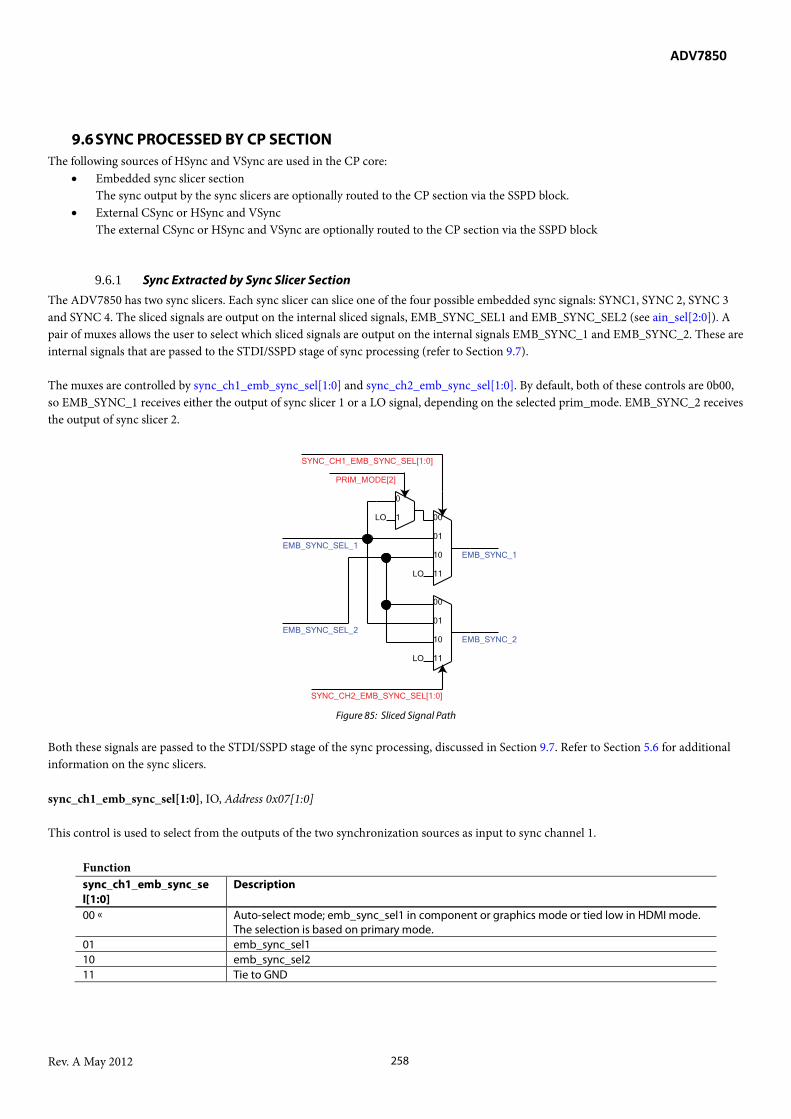
ADV7850
Rev. A May 2012 258
9.6 SYNC PROCESSED BY CP SECTION The following sources of HSync and VSync are used in the CP core:
• Embedded sync slicer section The sync output by the sync slicers are optionally routed to the CP section via the SSPD block.
• External CSync or HSync and VSync The external CSync or HSync and VSync are optionally routed to the CP section via the SSPD block
9.6.1 Sync Extracted by Sync Slicer Section The ADV7850 has two sync slicers. Each sync slicer can slice one of the four possible embedded sync signals: SYNC1, SYNC 2, SYNC 3 and SYNC 4. The sliced signals are output on the internal sliced signals, EMB_SYNC_SEL1 and EMB_SYNC_SEL2 (see ain_sel[2:0]). A pair of muxes allows the user to select which sliced signals are output on the internal signals EMB_SYNC_1 and EMB_SYNC_2. These are internal signals that are passed to the STDI/SSPD stage of sync processing (refer to Section 9.7). The muxes are controlled by sync_ch1_emb_sync_sel[1:0] and sync_ch2_emb_sync_sel[1:0]. By default, both of these controls are 0b00, so EMB_SYNC_1 receives either the output of sync slicer 1 or a LO signal, depending on the selected prim_mode. EMB_SYNC_2 receives the output of sync slicer 2.
Figure 85: Sliced Signal Path
Both these signals are passed to the STDI/SSPD stage of the sync processing, discussed in Section 9.7. Refer to Section 5.6 for additional information on the sync slicers. sync_ch1_emb_sync_sel[1:0], IO, Address 0x07[1:0] This control is used to select from the outputs of the two synchronization sources as input to sync channel 1.
Function sync_ch1_emb_sync_sel[1:0]
Description
00 Auto-select mode; emb_sync_sel1 in component or graphics mode or tied low in HDMI mode. The selection is based on primary mode.
01 emb_sync_sel1 10 emb_sync_sel2 11 Tie to GND
EMB_SYNC_SEL_1
EMB_SYNC_SEL_2
0
1 00
11
10
01
LO
00
11
10
01
LO
PRIM_MODE[2]
SYNC_CH1_EMB_SYNC_SEL[1:0]
SYNC_CH2_EMB_SYNC_SEL[1:0]
EMB_SYNC_2
EMB_SYNC_1
LO

ADV7850
Rev. A May 2012 259
sync_ch2_emb_sync_sel[1:0], IO, Address 0x08[1:0] This control is used to select from the outputs of the two sync slicers as input to sync channel 2.
Function sync_ch2_emb_sync_sel[1:0]
Description
00 emb_sync_sel2 01 emb_sync_sel1 10 emb_sync_sel2 11 Tie to GND
9.6.2 External Sync and Sync from HDMI Section The CP section can receive syncs from the external HSync, VSync and CSync inputs or from the HDMI section, as shown in Figure 86. The external sync signals from the HDMI are used for STDI detection. Note also that Figure 86 shows the routing of the internal embedded sync signals, EMB_SYNC_1 and EMB_SYNC_2, which are output by the sync slicers.
Figure 86: External/HDMI Syncs Routing to CP Section
9.6.2.1 Signals Routing to Synchronization Channels The ADV7850 has two synchronization channels. Each channel consists of one SSPD and one STDI section. When an HDMI input is applied, the HDMI core will generate HSync, VSync, and DE signals and supply them as input to each synchronization channel shown in Figure 86. HSync from the HDMI block is denoted as HDMI_HS, and VSync from the HDMI block is denoted as HDMI_VS. As well as the HDMI sync signals, external CSync or HSync and VSync signals applied to the pins are provided as inputs to the HSync and VSync muxes.
0 1 0 0
1 1 1 0 0 1
P R I M_M O D E [ 2 ]
H S / C S _ I N 1
HD M I H S
0 0
1 1 1 0 0 1
SY NC _ CH 1 _ H S _ SE L [ 1 : 0 ]
SY NC _ CH 2 _ H S _ SE L [ 1 : 0 ]
0 1 0 0
1 1 1 0 0 1
P R I M_M O D E [ 2 ]
VS _ I N 1
HD M I V S
0 0
1 1 1 0 0 1
SY NC _ CH 1 _ VS _ SE L [ 1 : 0 ]
SY NC _ CH 2 _ VS _ SE L [ 1 : 0 ]
E M B _ SY NC _ 2
E M B _ SY NC _ 1
H S / C S 1
H S / C S 2
VS 1
VS 2
E M B _ SY NC _ 1
H S / C S 1 _ G R VS 1
E M B _ SY NC _ 2 _ G R
VS 2 _ G R E M B _ SY NC _ 2
S T D I 1
SSP D 1
SSP D 2
HS1_GR_PC VS1_GR_PC
S T D I 2
CH 1 _ SSP D _ C O N T
CH 1 _ T R IG _ SSP D
CH 2 _ T R IG _ SSP D
CH 1 _ SY NC _ S RC [ 1 : 0 ]
CH 1 _ P O L _M A N _ E N
CH 2 _ P O L _M A N _ E N
CH 1 _ P O L _ V S
CH 2 _ P O L _ V S CH 2 _ P O L _ H S C S
CH 1 _ P O L _ H S C S
SY NC _ CH 1 _ P R IO R I T Y SYNC_CH_AUTO_MODE
VS _ P C
H S _ P C
XT
AL
CLO
CK
RE
GIS
TE
RIN
G B
LOC
K a
nd D
IGIT
AL
GLI
TC
H R
EJE
CT
ION
FIL
TE
R
D IG _ SY NC _ D E G L I T CH _ R E DUC E D IG SY NC D E G L I T CH R E DUC E M A N
T O SY NC
H S / C S 1
VS 1 _ G R
E M B _ SY NC _ 1 _ G R
P O L A R I T Y C O RR E C T IO N
H S 1 _ P C VS 1 _ P C
VS 2
H S / C S 2 H S / C S 2 _ G R
HS2_GR_PC
H S 2 _ P C VS 2 _ P C
P O L A R I T Y C O RR E C T IO N
T O SY NC
E M BE DD E D _ SY NC _M O D E1
E M BE DD E D _ SY NC _M O D E2
T O SY NC E M BE DD E D _ SY NC _M O D E
H S / C S _ I N 2
VS _ I N 2
CH1_SSPD_PP_EN
CH2_SSPD_CONT
CH2_SSPD_PP_EN CH2_SYNC_SRC[1:0]
VS2_GR_PC

ADV7850
Rev. A May 2012 260
Two muxes are used to select HSync /CSync 1 and HSync /CSync 2 from the three possible HSync signals. Similarly, two muxes are used to select VSync 1 and VSync 2 from the three possible VS signals. These muxes are controlled by sync_ch1_hs_sel[1:0], sync_ch1_vs_sel[1:0], sync_ch2_hs_sel[1:0], and sync_ch2_vs_sel[1:0]. The outputs of these four muxes, as well as the internal EMB_SYNC_1 and EMB_SYNC_2 signals from the sync slicers (as described in Section 9.6.1) are passed to a clock registering and deglitch block. sync_ch1_hs_sel[1:0], IO, Address 0x07[5:4] This control is used to select the HSync input to sync channel 1.
Function sync_ch1_hs_sel[1:0] Description 00 Auto-select mode; hs_in1 or HSync from HDMI (HDMI-HS) set to channel 1 based on primary
mode set in prim_mode[3:0]. HDMI-HS selected in HDMI mode. HS1 input selected in component or graphics mode.
01 Select hs_in1 10 Select hs_in2 11 HDMI-HS
sync_ch1_vs_sel[1:0], IO, Address 0x07[3:2] This control is used to select the VSync input to sync channel 1.
Function sync_ch1_vs_sel[1:0] Description 00 Auto-select mode; vs_in1 or VSync from HDMI (HDMI-VS) set to channel 1 based on primary
mode set in prim_mode[3:0]. HDMI-VS selected in HDMI mode. VS1 input selected in component or graphics mode.
01 Select vs_in1 input 10 Select vs_in2 input 11 Reserved
sync_ch2_hs_sel[1:0], IO, Address 0x08[5:4] This control is used to select the HSync input to sync channel 2.
Function sync_ch2_hs_sel[1:0] Description 00 Select HS2 input 01 Select HS1 input 10 Select HS2 input 11 Select HDMI HS
sync_ch2_vs_sel[1:0], IO, Address 0x08[3:2] This control is used to select the VSync input to sync channel 2.
Function sync_ch2_vs_sel[1:0] Description 00 Select VS2 input 01 Select VS1 input 10 Select VS2 input 11 Select HDMI VS
9.6.2.2 XTAL Clock Registering and Glitch Rejection Filter As shown in Figure 86, the XTAL CLOCK REGISTERING BLOCK and DIGITAL GLITCH REJECTION FILTER have two outputs for

ADV7850
Rev. A May 2012 261
each input. Each output has two instances, one with the same name as the input, and one with _GR at the end of the name. The _GR signals are latched by the XTAL clock and have a digital filter applied to them, whereas the output signals with the same name as the input signals are true bypass versions of the input signals; they are not latched by XTAL and they do not have any filtering applied to them. The _GR signals will have a glitch rejection filter applied to them. The filter can be controlled by the dig_sync_deglitch_reduce and dig_sync_deglitch_reduce_man signals. When dig_sync_deglitch_reduce_man is set to 0, the block automatically removes any sync signals that are less than five XTAL clocks wide for component inputs up to and including 1080i, and sync signals that are less than two XTAL clocks wide for component input 1080p and graphics standards. When this bit is set to 1, the user can select the filter to reduce syncs that are less than five XTAL clocks wide, or less than two XTAL clocks wide by setting dig_sync_deglitch_reduce to 0 or 1 respectively. dig_sync_deglitch_reduce, Addr 44 (CP), Address 0xF5[3] This control is used to configure the deglitch filters that process synchronization signals before they are input to the SSPD section. The value set is effective if dig_sync_deglitch_reduce_man is set to 1.
Function dig_sync_deglitch_reduce
Description
1 Remove 2 xtal clock wide glitches from synchronization signals input to SSPD sections 0 Remove 5 xtal clock wide glitches from synchronization signals input to SSPD sections
dig_sync_deglitch_reduce_man, Addr 44 (CP), Address 0xF5[2] This control is used to manually configure the deglitch filters that process synchronization signals input to the SSPD sections.
Function dig_sync_deglitch_reduce_man
Description
1 Manual configuration: deglitch filters configured via dig_sync_deglitch_reduce 0 Automatic configuration: deglitch filters remove 5 xtal clock wide glitches from
synchronization signals input to SSPD section
9.6.2.3 Signal Routed to SSPD Blocks The SSPD block from each synchronization channel receives six input signals, namely HS, HS_GR, VS, VS_GR, EMB_SYNC, and EMB_SYNC_GR. SSPD analyses the _GR signals to determine which signals have valid sync information, and will ‘correct’ the polarity of the syncs. In this instance, the definition of a ‘correct’ sync polarity is ‘negative going’, so for input formats with positive going syncs, these syncs will be inverted. The outputs from the SSPD section are the signals whose names end with _PC. These signals are the polarity corrected version of the syncs signals input to the SSPD sections. The SSPD block will pass a corrected, registered, glitch rejected HSync and VSync signal to the STDI block. Note that for embedded sync inputs or external CSync inputs where both HSync and VSync information are contained in one signal, the same signal will be applied to both inputs of the STDI block. The SSPD block will also pass a corrected HS and VS signal to the final mux shown on the right side of Figure 86, as well as a signal called EMBEDDED_SYNC_MODE which tells the CP core if the source of the HS_PC and VS_PC signals are from an embedded signal or separate signals. These syncs are polarity corrected but are not XTAL registered, nor are they glitch rejected. The final mux shown in Figure 86 selects between the HSync and VSync (and embedded sync information signal) from sync channel 1 and sync channel 2. Various controls exist to select how the SSPD block works, and which sync channel is passed to the CP core. These controls are described in detail in Section 9.7. Note that the syncs signals VS_PC and HS_PC passed to the CP core are polarity corrected but not XATL registered and glitch rejected. However, internally in the CP core, a glitch rejection filter is applied which rejects any sync signals less than seven CP clocks in width.

ADV7850
Rev. A May 2012 262
This glitch filter is not controllable.
9.6.3 Final Sync Muxing Stage As described in Section 9.6, the main source for sync information into the CP core is the SSPD block. Figure 87 shows the final stage of muxing, which selects the syncs to be used in the CP core. HSync and VSync signals from the selected SSPD block are passed through the glitch rejection filters. Then, depending on whether or not the input was an embedded sync signal type (external CS or SOG/SOY), VS is generated by the VSync slicer block. For CS/SOG/SOY input types, the embedded sync signal must be sliced to find the VS signal, but this should not be done for separate HS and VS inputs. Therefore, the EMBEDDED_SYNC_MODE control signal that is sent from the SSPD block is used to control a mux to bypass the VSync slicer block when the input is external HSync and VSync.
Figure 87: Final Sync Muxing Stage
9.7 SYNCHRONIZATION PROCESSING CHANNEL MUX The ADV7850 has two synchronization processing channels, as shown in Figure 86. These contain SSPD and the STDI functionality that receives synchronization, as described in Section 9.6.2.1. As explained in Section 9.6.2.1, channel 1 and channel 2 are identical in that they consist of the same basic SSPD and STDI blocks. However, they differ in the way in which the signals are multiplexed so that any synchronization source can be routed to any of the synchronization channels. By default, the synchronization channels are configured into the following two sets:
• Set 1: HS_IN1, VS_IN1, HDMI_HS and EMB_SYNC_1 feed synchronization channel 1 • Set 2: HS_IN2, VS_IN2, HDMI_VS and EMB_SYNC_2 feed synchronization channel 2
The registers that control the synchronization signals routed to each synchronization channel are described in Section 9.6.1 and Section 9.6.2.1. The output from one synchronization channel is used to provide timing to the CP core.. The method for determining the sync channel used to output synchronization signals to the CP core is selected by sync_ch_auto_mode. This bit is used to enable and disable the channel auto mode and works in conjunction with sync_ch1_priority, as follows:
• sync_ch_auto_mode = 0 The priority of the channels is determined by sync_ch1_priority: sync_ch1_priority = 1: Select channel 1 sync_ch1_priority = 0: Select channel 2
• sync_ch_auto_mode = 1
The synchronization channel that outputs sync signals to the CP core is automatically selected and based on the free run status of each channel. The priority of selection is determined by sync_ch1_priority: sync_ch1_priority = 1: Priority for channel 1 – free run if both channels are in free run and monitor channel 1. sync_ch1_priority = 0: Priority for channel 2 – free run if both channels are in free run and monitor channel 2.
VSYNC SLICER VS_PC
HS_PC TO CP CORE
0
1 VSYNC GLITCH
REJECTION FILTER TO CP CORE
EMBEDDED_SYNC_MODE
HSYNC GLITCH
REJECTION FILTER

ADV7850
Rev. A May 2012 263
sync_ch_auto_mode, IO, Address 0x07[7] This control is used to set automatic synchronization channel selection to the CP core. Auto mode selects which synchronization channel drives the CP based on the free run status of each channel. The priority of selection is determined by SYNC_CH1_PRIORITY when both channels are in free run mode.
Function sync_ch_auto_mode Description 0 Disable auto mode 1 Enable auto mode
sync_ch1_priority, IO, Address 0x07[6] This control is used to select which sync channel has priority to the CP core.
Function sync_ch1_priority Description 0 Sync channel 2 processing result takes priority 1 Sync channel 1 sync processing result takes priority
Refer to Section 9.12 for a detailed explanation of free run mode. The output from the synchronization channel multiplexing can be read from the SEL_SYNC_CHANNEL bit in the IO Map. sel_sync_channel, IO, Address 0x12[7] (Read Only) This readback indicates the currently selected sync processing channel applied to the CP core.
Function sel_sync_channel Description 0 Sync channel 2 processed by CP core 1 Sync channel 1 processed by CP core
9.7.1 Synchronization Source Polarity Detector Section 9.7 describes how the various synchronization signals are routed to the two synchronization processing channels. Each of these channels employs an SSPD block to enable it to determine where the synchronization source comes from, and its polarity. The functions of an SSPD block are:
• Automatic detection of the active synchronization source
• Automatic detection of the synchronization polarity, if applicable
• Readback on SSPD manual override for the synchronization source through synchronization channel multiplexing, as described in Section 9.7
• Manual override for polarity detection via chx_pol_man_en (where x refers to either 1 or 2) The SSPD block can operate either in continuous or in single-shot mode. Continuous mode means that the block permanently monitors the inputs and updates its outputs. In single-shot mode, the SSPD block waits for a 0 to 1 transition on the chx_trig_sspd bit (where x refers to either 1 or 2) before it scans the synchronization inputs once. Single-shot operation is useful to avoid system scheduling conflicts. The SSPD state machine searches for active synchronization signals in the following order of priority:
1. External HSync/VSync 2. External CSync 3. Embedded synchronization
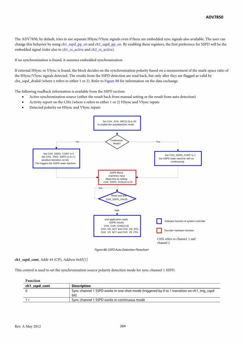
ADV7850
Rev. A May 2012 264
The ADV7850, by default, tries to use separate HSync/VSync signals even if there are embedded sync signals also available. The user can change this behavior by using ch1_sspd_pp_en and ch2_sspd_pp_en. By enabling these registers, the first preference for SSPD will be the embedded signal (refer also to ch1_rs_active and ch2_rs_active). If no synchronization is found, it assumes embedded synchronization. If external HSync or VSync is found, the block decides on the synchronization polarity based on a measurement of the mark-space ratio of the HSync/VSync signals detected. The results from the SSPD detection are read back, but only after they are flagged as valid by chx_sspd_dvalid (where x refers to either 1 or 2). Refer to Figure 88 for information on the data exchange. The following readback information is available from the SSPD section:
• Active synchronization source (either the result back from manual setting or the result from auto detection) • Activity report on the CHx (where x refers to either 1 or 2) HSync and VSync inputs • Detected polarity on HSync and VSync inputs
Figure 88: SSPD Auto Detection Flowchart
ch1_sspd_cont, Addr 44 (CP), Address 0x85[1] This control is used to set the synchronization source polarity detection mode for sync channel 1 SSPD.
Function ch1_sspd_cont Description 0 Sync channel 1 SSPD works in one-shot mode (triggered by 0 to 1 transition on ch1_trig_sspd
bit) 1 Sync channel 1 SSPD works in continuous mode
end application reads SSPD results
CHX_CUR_SYNC[1:0] CHX_HS_ACT and CHX_HS_POL CHX_VS_ACT and CHX_VS_POL
SSPD Block examines input
(flags this by setting CHX_SSPD_DVALID to 0)
Set CHX_SYN_SRC[1:0] to 00 to enable the autodetection mode
Read and test CHX_SSPD_VALID
low
high
Software function of system controller
Decoder hardware function
Set CHX_SSPD_CONT to 1 the SSPD state machine will run
continuously Set CHX_SSPD_CONT to 0
Set CHX_TRIG_SSPD to 0=>1 (positive transition on bit)
This triggers the SSPD state machine
Continuous Mode? No Yes
CHX refers to channe1 1 and channel 2

ADV7850
Rev. A May 2012 265
ch2_sspd_cont, Addr 44 (CP), Address 0x41[1] This control is used to set the synchronization source polarity detection mode for sync channel 2 SSPD.
Function ch2_sspd_cont Description 0 Sync channel 2 SSPD works in one-shot mode (triggered by a 0 to 1 transition on
ch2_trig_sspd bit) 1 Sync channel 2 SSPD works in continuous mode
ch1_trig_sspd, Addr 44 (CP), Address 0x85[2] This control is used to trigger a synchronization source and polarity detector for sync channel 1 SSPD. A 0 to 1 transition in this bit restarts the autosync detection algorithm. This is not a self clearing bit and must be set to 0 to prepare for the next trigger.
Function ch1_trig_sspd Description 0 Default - transition 0 to 1 restarts autosync detection algorithm 1 Transition 0 to 1 restarts autosync detection algorithm
ch2_trig_sspd, Addr 44 (CP), Address 0x41[2] This control is used to trigger a synchronization source and polarity detector for sync channel 2 SSPD. A 0 to 1 transition in this bit restarts the autosync detection algorithm. This is not a self clearing bit and must be set to 0 to prepare for the next trigger.
Function ch2_trig_sspd Description 0 Default - transition 0 to 1 restarts autosync detection algorithm 1 Transition 0 to 1 restarts autosync detection algorithm
ch1_sync_src[1:0], Addr 44 (CP), Address 0x85[4:3] This control is used to select the synchronization signals processed by sync channel 1 SSPD.
Function ch1_sync_src[1:0] Description 00 Autodetect mode for synchronization source. Use results of autodetection for synchronization
signal routing. Result can be read back via ch1_cur_sync[1:0] bits. 01 Manual setting: separate HSync and VSync to sync channel 1 SSPD. 10 Manual setting
ch2_sync_src[1:0], Addr 44 (CP), Address 0x41[4:3] This control is used to select the synchronization signals processed by sync channel 2 SSPD.
Function ch2_sync_src[1:0] Description 00 Autodetection mode for synchronization source. Use results of autodetection for
synchronization signal routing. Result can be read back via ch2_cur_sync[1:0] bits. 01 Manual setting: separate HSync and VSync to sync channel 2 SSPD. 10 Manual sett
ch1_pol_man_en, Addr 44 (CP), Address 0x85[7] This control is used to override for polarity detection by sync channel 1 SSPD. ch1_pol_man_en must be set to 1 for this control to become active.

ADV7850
Rev. A May 2012 266
Function ch1_pol_man_en Description 0 Use result from sync channel 1 SSPD polarity autodetection 1 Manual override, use ch1_pol_vs and ch1_pol_hs
ch2_pol_man_en, Addr 44 (CP), Address 0x41[7] This control is used to override the polarity detection by sync channel 2 SSPD.
Function ch2_pol_man_en Description 0 Use result from sync channel 2 SSPD autodetection 1 Use ch2_pol_vs and ch2_pol_hs
ch1_pol_vs, Addr 44 (CP), Address 0x85[6] This control is used to override the polarity of VSync by sync channel 1 SSPD.
Function ch1_pol_vs Description 0 VSync input to sync channel 1 carries negative polarity signal 1 VSync input to sync channel 1 carries positive polarity signal
ch2_pol_vs, Addr 44 (CP), Address 0x41[6] This control is used to override the polarity of VSync by sync channel 2 SSPD. ch2_pol_man_en must be set to 1 for this control to be active.
Function ch2_pol_vs Description 0 VSync input to sync channel 2 carries negative polarity signal 1 VSync input to sync channel 2 carries positive polarity signal
ch1_pol_hscs, Addr 44 (CP), Address 0x85[5] This control is used to override the polarity of HSync by sync channel 1 SSPD. ch1_pol_man_en must be set to 1 for this control to become active.
Function ch1_pol_hscs Description 0 HSync input to sync channel 1 carries negative polarity signal (HSync or CSync) 1 HSync input to sync channel 1 carries positive polarity signal (HSync or CSync)
ch2_pol_hscs, Addr 44 (CP), Address 0x41[5] This control is used to override the polarity of HSync by sync channel 2 SSPD. ch2_pol_man_en must be set to 1 for this control to be active.
Function ch2_pol_hscs Description 0 HSync input to sync channel 2 carries negative polarity signal (HSync or CSync) 1 HSync input to sync channel 2 carries positive polarity signal (HSync or CSync)

ADV7850
Rev. A May 2012 267
emb_sync_on_all, Addr 44 (CP), Address 0x67[5] This control is used to alter the gain computed by the AGC based on the presence of an embedded synchronization on channels A, B and C. It is used only in the case of RGB input and RGB output with color controls enabled.
Function emb_sync_on_all Description 0 Embedded synchronization present only on luma channel (i.e. channel A) 1 All three input channels have embedded synchronization
ch1_sspd_pp_en, Addr 44 (CP), Address 0x84[1] This control is used to enable sync channel 1 SSPD post processing.
Function ch1_sspd_pp_en Description 0 Disable post processing of synchronization signals input to sync channel 1 SSPD 1 Check for activity on embedded synchronization signal input to sync channel 1 SSPD when it
detects activity on HSync, CSync and VSync. Activity on embedded signal input to sync channel 1 SSPD reported by ch1_rs_active. Post processing of synchronization signal input to sync channel 1 SSPD works only if timing on embedded synchronization signal and timing on HSync/CSync and VSync signals are same.
ch2_sspd_pp_en, Addr 44 (CP), Address 0x41[0] This control is used to enable sync channel 2 SSPD post processing. Activity on the embedded signal input to sync channel 2 SSPD is reported by ch2_rs_active. Post processing of the synchronization signal input to sync channel 2 SSPD works only if the embedded synchronization signal and the HSync/CSync and VSync signals have the same timing.
Function ch2_sspd_pp_en Description 0 Disable post processing of synchronization signals input to sync channel 2 SSPD 1 Check for activity on embedded synchronization signal input to sync channel 2 SSPD when it
detects activity on HSync/CSync and VSync
9.7.1.1 SSPD Readback Signals
ch1_sspd_dvalid, Addr 44 (CP), Address 0xB5[7] (Read Only) This control is set to 1 when the readbacks from the SSPD section of the synchronization sync channel 1 are valid. It is set to 1 after 2^22 crystal clock periods following a reset of the CP section. It is set to 0 when the device is reset.
Function ch1_sspd_dvalid Description 0 Sync channel 1 SSPD results not valid for readback 1 Sync channel 1 SSPD results valid
ch2_sspd_dvalid, Addr 44 (CP), Address 0x4F[7] (Read Only) This control is set to 1 when the readbacks from the SSPD section of sync channel 2 are valid. It is set to 1 after 2^22 crystal clock periods following a reset of the CP section. It is set to 0 when the DUT is reset.
ADV7850
Rev. A May 2012 268
Function ch2_sspd_dvalid Description 0 Sync channel 2 SSPD results not valid for readback 1 Sync channel 2 SSPD results valid (detection finished)
ch1_cur_sync_src[1:0], Addr 44 (CP), Address 0xB5[1:0] (Read Only) This readback displays the current synchronization source detected by sync channel 1 SSPD.
Function ch1_cur_sync_src[1:0] Description 00 Not used 01 Activity detected on HSync and VSync input to sync channel 1 SSPD 10 CSync detected on HSync input to sync channel 1 SSPD 11 Activity detected on embedded synchronization input to sync channel 1 SSPD
ch2_cur_sync_src[1:0], Addr 44 (CP), Address 0x4F[1:0] (Read Only) This readback displays the current synchronization source detected by sync channel 2 SSPD.
Function ch2_cur_sync_src[1:0] Description 00 Not used 01 Activity detected on HSync and VSync input to sync channel 2 SSPD 10 CSync detected in HSync input to sync channel 2 SSPD 11 Activity detected on embedded synchronization input to sync channel 2 SSPD
ch1_cur_pol_hs, Addr 44 (CP), Address 0xB5[3] (Read Only) This readback indicates the polarity of the HSync/CSync input to the sync channel 1 SSPD.
Function ch1_cur_pol_hs Description 0 Negative polarity on HSync/CSync input to sync channel 1 SSPD 1 Positive polarity on HSync/CSync input to sync channel 1 SSPD
ch2_cur_pol_hs, Addr 44 (CP), Address 0x4F[3] (Read Only) This readback displays the polarity of the HSync/CSync input to sync channel 2 SSPD.
Function ch2_cur_pol_hs Description 0 HSync CSync input to sync channel 2 SSPD has negative polarity 1 HSync CSync input to sync channel 2 SSPD has positive polarity
ch1_hs_act, Addr 44 (CP), Address 0xB5[4] (Read Only) This readback indicates activity on the HSync/CSync input to sync channel 1 SSPD.
Function ch1_hs_act Description 0 No activity detected on HSync/CSync input to sync channel 1 SSPD 1 HSync/CSync input to sync channel 1 SSPD carries an active signal
The SSPD section continuously monitors the HSync input signal over timing windows of 222 crystal clock periods (refer to Figure 89). ch1_hs_act is updated at the end of each window, as follows:

ADV7850
Rev. A May 2012 269
• ch1_hs_act is set to 1 if the SSPD has detected eight edges or four periods on the HSync signal • ch1_hs_act is set to 0 if the SSPD has detected less than eight edges or four periods on the HSync signal
ch2_hs_act, Addr 44 (CP), Address 0x4F[4] (Read Only) This readback displays activity on the HSync/CSync input to sync channel 2 SSPD.
Function ch2_hs_act Description 0 No activity detected on HSync/CSync input to sync channel 2 SSPD 1 HSync/CSync input to sync channel 2 SSPD carries an active signal
ch1_cur_pol_vs, Addr 44 (CP), Address 0xB5[5] (Read Only) This readback indicates polarity on the HSync/CSync input to sync channel 1 SSPD.
Function ch1_cur_pol_vs Description 0 VSync input to sync channel 1 SSPD has negative polarity signal 1 VSync input to sync channel 1 SSPD has positive polarity signal
ch2_cur_pol_vs, Addr 44 (CP), Address 0x4F[5] (Read Only) This readback displays the polarity of the VSync input to sync channel 2 SSPD.
Function ch2_cur_pol_vs Description 0 VSync input to sync channel 2 SSPD has negative polarity signal 1 VSync input to sync channel 2 SSPD has positive polarity signal
ch1_vs_act, Addr 44 (CP), Address 0xB5[6] (Read Only) This readback indicates activity on VSync input to sync channel 1 SSPD.
Function ch1_vs_act Description 0 No activity detected on VSync input to sync channel 1 SSPD 1 VSync input to sync channel 1 SSPD carries an active signal
The SSPD section continuously monitors the VSync input signal over timing windows of 222 crystal clock periods (refer to Figure 89). ch1_vs_act is updated at the end of each window, as follows:
• ch1_vs_act is set to 1 if the SSPD detected four edges or two periods on the VSync signal • ch1_vs_act is set to 0 if the SSPD detected less than four edges or two periods on the VSync signal
ch2_vs_act, Addr 44 (CP), Address 0x4F[6] (Read Only) This readback indicates the activity on the VSync input to sync channel 2 SSPD.

ADV7850
Rev. A May 2012 270
Function ch2_vs_act Description 0 No activity detected on VSync input to sync channel 2 SSPD 1 VSync input to sync channel 2 SSPD carries an active signal
The SSPD section continuously monitors the VSync input signal over timing windows of 222 crystal clock periods (refer to Figure 89). ch2_vs_act is updated at the end of each window as follows:
• ch2_vs_act is set to 1 if the SSPD detected four edges or two periods on the VSync signal • ch2_vs_act is set to 0 if the SSPD detected less than four edges or two periods on the VSync signal
Figure 89: SSPD VSync and HSync Monitoring Operation
ch1_rs_active, Addr 44 (CP), Address 0xB5[2] (Read Only) This readback indicates activity in the embedded synchronization signal input to sync channel 1 SSPD. ch1_sspd_pp_en must be set to 1 and ch1_sspd_dvalid must return 1 for this readback to be valid.
Function ch1_rs_active Description 0 Activity detected on embedded signal input to sync channel 1 SSPD 1 No activity detected on embedded signal input to sync channel 1 SSPD
ch2_rs_active, Addr 44 (CP), Address 0x4F[2] (Read Only) This readback displays activity in an embedded synchronization signal input to sync channel 2 SSPD. ch2_sspd_pp_en must be set to 1 and ch2_sspd_dvalid must return 1 for this readback to be valid. This readback is only valid when there is an HSync and VSync signal present. It is not valid to use this control when only an embedded signal is present. The purpose of this control is to indicate that the user can switch to embedded sync if using HSync and VSync inputs.
Function ch2_rs_active Description 0 Activity detected on embedded signal input to sync channel 2 SSPD 1 No activity detected on embedded signal input to sync channel 2 SSPD
Notes:
• It is possible to monitor changes in ch1_vs_act, ch1_hs_act and ch1_rs_activE via the sspd_rslt_chngd_ch1_st interrupt status. • Likewise, it is possible to monitor changes in ch2_vs_act, ch2_hs_act, and ch2_rs_active via the sspd_rslt_chngd_ch2_st
interrupt status. sspd_rslt_chngd_ch1_st, IO, Address 0x5C[0] (Read Only) This readback indicates the latched signal status of the SSPD result changed for sync channel 1 interrupt signal. Once set, this bit remains high until the interrupt is cleared via sspd_rslt_chngd_ch1_clr. This bit is only valid if enabled via the corresponding INT1 or INT2 interrupt mask bit.
Field 3 or Line 3 Field 4 or Line 4 Field 5 or Line 5 Field 6 or Line 6
SSPPD monitors activity on each sync signal VS and HS over a 222 crystal clock cycles window 222 crystal clock cycles window222 crystal clock cycles window
Field 1 or Line 1 Field 7 or Line 7Field 2 or Line 2

ADV7850
Rev. A May 2012 271
Function sspd_rslt_chngd_ch1_st Description 0 No SSPD result changed for sync channel 1 interrupt event occurred 1 SSPD result changed for sync channel 1 interrupt event occurred
sspd_rslt_chngd_ch1_raw, IO, Address 0x5B[0] (Read Only) Status of the SSPD Result Changed on sync channel 1 interrupt signal. When set to 1 it indicates a change in SSPD result of the currently selected sync channel. A change in SSPD result can be either due to a polarity or source change. Once set, this bit will remain high until it is cleared via sspd_rslt_chngd_ch1_clr.
Function sspd_rslt_chngd_ch1_raw
Description
0 No change in SSPD result for sync channel 1 1 Change occurred in SSPD result for sync channel 1
sspd_rslt_chngd_ch2_st, IO, Address 0x5C[4] (Read Only) This readback indicates the latched signal status of the SSPD result changed for sync channel 2 interrupt signal. Once set, this bit remains high until the interrupt is cleared via sspd_rslt_chngd_ch2_clr. This bit is only valid if enabled via the corresponding INT1 or INT2 interrupt mask bit.
Function sspd_rslt_chngd_ch2_st Description 0 No SSPD result changed for sync channel 2 interrupt event occurred 1 SSPD result changed for sync channel 2 interrupt event occurred
sspd_rslt_chngd_ch2_raw, IO, Address 0x5B[4] (Read Only) This readback indicates the status of the SSPD result changed on sync channel 2 interrupt signal. When set to 1, it indicates a change in SSPD result of the currently selected sync channel. A change in SSPD result can be either due to a polarity or source change. Once set, this bit will remain high until it is cleared via sspd_rslt_chngd_ch1_clr.
Function sspd_rslt_chngd_ch2_raw
Description
0 No change in SSPD result for sync channel 2 1 Change occurred in SSPD result for sync channel 2
9.7.2 Standard Detection and Identification As shown in Figure 86, the two synchronization processing channels also contain Standard Detection and Identification (STDI) blocks. These monitor the synchronization signals to determine the video input standard. The STDI blocks perform four key measurements:
• Block Length chx_bl[13:0] This is the number of 27 MHz clock cycles (XTAL frequency) in a block of eight lines. From this, the time duration of one line can be concluded.
• Line Count in Field chx_lcf[10:0] The chx_lcf[10:0] readback value is the number of lines between two VSyncs, that is, over one field measured by channel x.
• Line Count in VSync chx_lcvs[4:0] The lcvs[4:0] readback value is the number of lines within one VSync period.
• Field Length chx_fcl[12:0] This is the number of 27 MHz clock cycles in a 1/256th of a field. Alternately, this value of FCL multiplied by 256 gives one field
ADV7850
Rev. A May 2012 272
length count in 27 MHz (XTAL) clocks. Note: chx is CH1 or CH2 in the above descriptions, representing channel 1 and channel 2 related registers. By interpreting these four parameters, it is possible to derive the applied video signal horizontal and vertical resolution information and determine its standard. In ADV7850, there are three operational modes for the STDI block:
• Continuous mode: The STDI block performs continuous measurements on a lock/unlock basis and updates the corresponding IP
2PC registers based
on the lock status bit (stdi_dvalid). • Real-time continuous mode:
The STDI block performs continuous measurement regardless of the lock/unlock basis and always updates real-time measurement data to the corresponding I2C registers.
• Single shot mode: The STDI block waits for a trigger (0 to 1 transition on chx_trig_stdi) to start the measurements. Single-shot mode can be useful in complex systems where the scheduling of functions is important.
A data valid flag, chx_stdi_dvalid, is provided, which is based on the status of the horizontal/vertical lock of the block and is held low during the measurements. The four parameters should only be read after the chx_stdi_dvalid flag has gone high for the continuous/single shot mode. In real-time continuous mode, the ADV7850 allows the user to monitor the real-time timing measurement regardless of the chx_stdi_dvalid flag. Refer to Section 9.7.3.4 for information on the readback values. Notes:
• Synchronization type pulses include horizontal synchronization, equalization and serration pulses, and Macrovision pulses. • Macrovision pseudo synchronization and AGC pulses are counted by the STDI block in normal readback mode. This does not
prohibit the identification of the video signal. • chx_trig_stdi is not self clearing. The measurements are only started upon setting chx_trig_stdi. This means that after setting it,
it must be cleared again by writing a 0 to it. This second write (to clear it) can be done at any time and does not have any effect on running measurements. It also does not invalidate previous measurement results.
• The ADV7850 only measures those parameters, but does not take any action based upon them. The part does not reconfigure itself. To avoid unforeseen problems in the scheduling of a system controller, the part merely helps to identify the input.
• Since real-time continuous mode provides the capability to monitor the real-time measurement data regardless of the block lock status, the user should be aware that the timing readback values may not be a valid readback measurement in this mode.
ch1_stdi_cont, Addr 44 (CP), Address 0x86[1] This control is used to set the synchronization source polarity detection mode for sync channel 1 STDI.
Function ch1_stdi_cont Description 0 Sync channel 1 STDI works in one-shot mode (triggered by 0 to 1 transition on ch1_trig_sspd) 1 Sync channel 1 STDI works in continuous mode
ch2_stdi_cont, Addr 44 (CP), Address 0x42[1] This control is used to select the sync channel 2 STDI mode of operation.
Function ch2_stdi_cont Description 0 Sync channel 2 STDI block operates in single-shot mode. 0 to 1 transition on ch2_trig_stdi
triggers measurement of sync channel 2 STDI block. 1 Sync channel 2 STDI runs in continuous mode.

ADV7850
Rev. A May 2012 273
bypass_stdi1_locking, Addr 44 (CP), Address 0xF5[1] This control is used to bypass STDI locking for sync channel 1.
Function bypass_stdi1_locking Description 0 Update ch1_bl, ch1_lcf and ch1_lcvs. Only sync channel 1 STDI locks and ch1_stdi_dvalid set
to 1. 1 Update ch1_bl, ch1_lcf and ch1_lcvs from sync channel 1 STDI as they are measured.
bypass_stdi2_locking, Addr 44 (CP), Address 0xF5[0] This control is used to bypass STDI locking for sync channel 2.
Function bypass_stdi2_locking Description 0 Update ch2_bl, ch2_lcf and ch2_lcvs. Only sync channel 2 STDI locks and ch2_stdi_dvalid set
to 1. 1 Update ch2_bl, ch2_lcf and ch2_lcvs from sync channel 2 STDI as they are measured.
ch1_trig_stdi, Addr 44 (CP), Address 0x86[2] This control is used to trigger a synchronization source and polarity detector for sync channel 1 STDI. A 0 to 1 transition in this bit restarts the autosync detection algorithm. This is not a self clearing bit and must be set to 0 to prepare for the next trigger.
Function ch1_trig_stdi Description 0 Default - transition 0 to 1 restarts autosync detection algorithm 1 Reset to zero to prepare for next trigger
ch2_trig_stdi, Addr 44 (CP), Address 0x42[2] This control is used to trigger the standard identification of sync channel 2 STDI. A 0 to 1 transition triggers the STDI measurements. This is not a self clearing bit and must be set to 0 to prepare for the next STDI measurements.
Function ch2_trig_stdi Description 0 Default - transition 0 to 1 restarts autosync detection algorithm 1 Transition 0 to 1 restarts autosync detection algorithm
ch1_stdi_dvalid, Addr 44 (CP), Address 0xB1[7] (Read Only) This readback is set when the measurements performed by sync channel 1 STDI are completed. A high level indicates ch1_bl, ch1_lcf, ch1_lcvs, ch1_fcl, and chi_stdi_intlcd are valid readback. To prevent false readouts, especially during signal acquisition, ch1_stdi_dvalid is set to 1 only after four fields with the same length are recorded. As a result, STDI measurements can take up to five fields to finish.
Function ch1_stdi_dvalid Description 0 Sync channel 1 STDI measurement not valid 1 Sync channel 1 STDI measurement valid
ch2_stdi_dvalid, Addr 44 (CP), Address 0x49[7] (Read Only) This control is set when the measurements performed by sync channel 2 STDI are completed. A high level signals validity for the ch2_blL, ch2_lcf, ch2_lcvs, ch2_fcl, and ch2_stdi_intlcd controls. To prevent false readouts, especially during signal acquisition,

ADV7850
Rev. A May 2012 274
ch2_sdti_dvalid is set to 1 only after four fields with the same length are recorded. As a result, STDI measurements can take up to five fields to finish.
Function ch2_stdi_dvalid Description 0 Sync channel 2 STDI measurement not valid 1 Sync channel 2 STDI measurement valid
9.7.3 Detailed Mechanism of STDI Block Horizontal/Vertical Lock Mechanism
9.7.3.1 STDI Horizontal Locking Operation For the STDI horizontal locking operation, the STDI block compares adjacent line length differences (in XTAL clock cycles) with the programmed threshold. If 128 consecutive adjacent lines lengths are within the threshold, the STDI horizontally locks to the incoming video.
Figure 90: STDI Horizontal Locking Operation
Once the STDI locks to the incoming video, it registers the first BL measurement (first eight lines) as latched data (absolute line length: L) and keeps monitoring and comparing each successive line length with the absolute line length (L/8). The STDI horizontally unlocks if 128 consecutive lines have a line length greater than the threshold.
Figure 91: STDI HSync Monitoring Operation
9.7.3.2 STDI Vertical Locking The STDI block compares adjacent field length differences and VSync lengths in line counts and compares them with a threshold. If four consecutive adjacent field lengths (LCF) and line counts in VSync (LCVS) are within the threshold, the STDI vertically locks to the incoming video.
line 1 line 2 line 3 line 4 line 5
line 1-line2≦threshold?
line 2-line3≦threshold?
line 3-line4≦threshold?
line 4-line5≦threshold?
line 5-line6≦threshold?
line 6 line 7 line 8 line 128
Monitors 128 consecutive lines before STDI horizontally ”Lock”
line 129line 1 line 2 line 3 line 4 line 5
line 1-line2≦threshold?
line 2-line3≦threshold?
line 3-line4≦threshold?
line 4-line5≦threshold?
line 5-line6≦threshold?
line 6 line 7 line 8 line 128
Monitors 128 consecutive lines before STDI horizontally ”Lock”
line 129
line 1 line 2 line 3 line 4 line 5 line 6 line 7 line 8
First 8 blocks of line length = BL read back valueRegistered as “Absolute Line Length”
line 128 line 129
line 129 – L/8 ≦threshold?
line 130 line 131
L line 130 – L/8 ≦threshold?
line 131 – L/8 ≦threshold?
“L/8” will be registered as absolute line length reference for each lines after STDI horizontally locks to the incoming video signal

ADV7850
Rev. A May 2012 275
Figure 92: STDI Vertical Locking Operation
Once the STDI locks to the incoming video, the STDI registers the latest field length/VSync length as latched data (absolute field length: F, absolute VSync length: V). The STDI keeps monitoring and comparing Field/VSync lengths with the respective absolute length (F, V) once vertically locked. The STDI vertically unlocks if four consecutive Field or VSync lengths are greater than the respective threshold.
Figure 93: STDI VSync Monitoring Operation
ch1_bl[13:0], Addr 44 (CP), Address 0xB1[5:0]; Address 0xB2[7:0] (Read Only) This readback displays the block length for sync channel 1. It displays the number of crystal clock cycles in a block of eight lines of incoming video. This readback is valid if ch1_stdi_dvalid is set to 1.
Function ch1_bl[13:0] Description xxxxxxxxxxxxxx Readback value
ch2_bl[13:0], Addr 44 (CP), Address 0x49[5:0]; Address 0x4A[7:0] (Read Only) This readback displays the sync channel 2 block length. It displays the number of crystal cycles in a block of eight lines of incoming video. The readback is valid if ch2_stdi_dvalid is set to 1.
Function ch2_bl[13:0] Description xxxxxxxxxxxxxx Readback value
ch1_lcvs[4:0], Addr 44 (CP), Address 0xB3[7:3] (Read Only) This readback displays the sync channel 1 line count in a VSync. It displays the number of lines in a VSync period measured on sync channel 1. The readback is valid if ch1_stdi_dvalid is set to 1.
Field1 – Field2 ≦threshold?
Vsync1 – Vsync2 ≦threshold?
Active Video Active Video Active Video Active Video
Field1 Field2 Field3 Field4
Vsync1 Vsync2 Vsync3 Vsync4
Active Video
Field5
Vsync5
Active Video
Field6
Vsync2 – Vsync3 ≦threshold?Vsync3 – Vsync4 ≦threshold?
Vsync5 – Vsync4 ≦threshold?
Field2– Field3 ≦threshold?
Field3 – Field4 ≦threshold?
Field4 – Field5 ≦threshold?
Active Video Active Video Active Video Active Video
Field1 Field2 Field3 Field4
Vsync1 Vsync2 Vsync3 Vsync4
Active VideoField5
Vsync5
Active VideoField6
Field5 – F ≦threshold?F
Latched Field Length Field6 – F ≦threshold?
Vsync5 – V ≦threshold?F
Latched Vsync Length
Active Video Active Video Active Video Active Video
Field1 Field2 Field3 Field4
Vsync1 Vsync2 Vsync3 Vsync4
Active VideoField5
Vsync5
Active VideoField6
Field5 – F ≦threshold?F
Latched Field Length Field6 – F ≦threshold?
Vsync5 – V ≦threshold?F
Latched Vsync Length

ADV7850
Rev. A May 2012 276
Function ch1_lcvs[4:0] Description xxxxx Readback value
ch2_lcvs[4:0], Addr 44 (CP), Address 0x4B[7:3] (Read Only) This readback displays the sync channel 2 line count in a VSync. It displays the number of lines in a VSync period measured on sync channel 2. The readback is valid if ch2_stdi_dvalid is set to 1.
Function ch2_lcvs[4:0] Description xxxxx Readback value
ch1_lcf[11:0], Addr 44 (CP), Address 0xA3[3:0]; Address 0xA4[7:0] (Read Only) This readback displays the sync channel 1 line count in a field. The number of lines between two VSyncs is measured on sync channel 1. The readback is valid if ch1_stdi_dvalid is set to 1.
Function ch1_lcf[11:0] Description xxxxxxxxxxx Readback value
ch2_lcf[11:0], Addr 44 (CP), Address 0x4B[2:0]; Address 0x4C[7:0]; Address 0x4D[7] (Read Only) This readback displays the sync channel 2 line count in a field. It displays the number of lines between two VSyncs measured on sync channel 2. The readback is valid if ch2_stdi_dvalid is set to 1.
Function ch2_lcf[11:0] Description xxxxxxxxxxx Readback value
ch1_fcl[12:0], Addr 44 (CP), Address 0xB8[4:0]; Address 0xB9[7:0] (Read Only) This readback displays the sync channel 1 field count length. It displays the number of crystal clock cycles between successive VSyncs measured by sync channel 1 STDI or in 1/256th of a field. The readback from this field is valid if ch1_stdi_dvalid is set.
Function ch1_fcl[12:0] Description xxxxxxxxxxxxx Readback value
ch2_fcl[12:0], Addr 44 (CP), Address 0x4D[4:0]; Address 0x4E[7:0] (Read Only) This readback displays the sync channel 2 field count length. The number of crystal clock cycles between successive VSyncs is measured by sync channel 2 STDI or in 1/256th of a field. The readback is valid if ch2_stdi_dvalid is set to 1.
Function ch2_fcl[12:0] Description xxxxxxxxxxxxx Readback value
ch1_stdi_intlcd, Addr 44 (CP), Address 0xB1[6] (Read Only) This readback displays interlaced versus progressive mode detected by sync channel 1 STDI. The readback is valid if ch1_stdi_dvalid is set to 1.

ADV7850
Rev. A May 2012 277
Function ch1_stdi_intlcd Description 0 Indicates video signal on sync channel 1 with non interlaced timing 1 Indicates signal on sync channel 1 with interlaced timing
ch2_stdi_intlcd, Addr 44 (CP), Address 0x49[6] (Read Only) This readback displays interlaced versus progressive mode detected by sync channel 2 STDI. The readback is valid if ch2_stdi_dvalid is set to 1.
Function ch2_stdi_intlcd Description 0 Indicates video signal on sync channel 2 with non interlaced timing 1 Indicates signal on sync channel 2 with interlaced timing
9.7.3.3 STDI Usage Figure 94 shows a flowchart of the intended usage of the STDI block.
Figure 94: STDI Usage Flowchart
9.7.3.4 STDI Readback Values for SD, PR, and HD Table 53: STDI Readback Values for SD, PR, and HD
Standard CHx_BL[13:0] 27 MHz XTAL
CHx_LCF[10:0] CHx_LCVS[4:0] FCL[12:0] 27 MHz XTAL
720p SMPTE 296M 4800 750 4 to 5 1761 1125i SMPTE 274M 6400 562 to 563 4 to 5 1761 525p BT 1358 6855 525 5 to 6 1761 625p BT 1358 6912 625 4 to 5 2109 1250i BT 709/SMPTE 295 6912 625 1 4218 1125i SMPTE 274M 6 7679 562 to 563 4 to 5 1761 1125p SMPTE 274M 10 800 1125 4 to 5 1761 525i SD 13728 262 to 263 3 1761 625i SD 13824 312 to 313 2 to 3 2109
End application reads video detection results
CHX_BL[13:0], CHX_LCVS[4:0], CHX_LCF[10:0] and CHX_FCL[12:0]
End application determines video standard and programs
prim_mode and VID_STD accordingly
STDI Block examines input
(flags this by setting CHX_STDI_DVALID to 0)
Set CHX_STDI_CONT to 0 Set CHX_TRIG_STDI to 0=>1
(positive transition on bit) to start the STDI state
machine
Read and CHX_STDI_DVALI
Low
High
No
Software function of system controller
Decoder hardware function
Continuous Mode?
Set CHX_STDI_CONT to 1 STDI state machine will run
continuously
Yes
Where CHX is CH1 for channel 1 or CHX is CH2 for channel 2
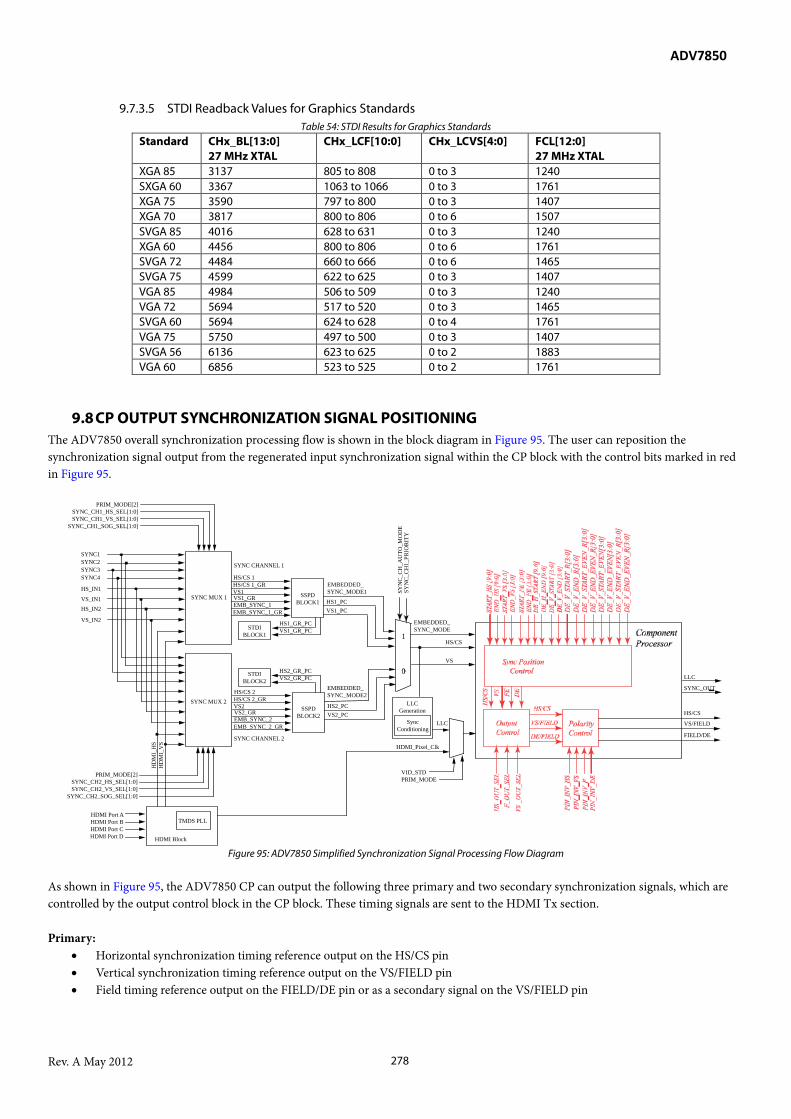
ADV7850
Rev. A May 2012 278
9.7.3.5 STDI Readback Values for Graphics Standards Table 54: STDI Results for Graphics Standards
Standard CHx_BL[13:0] 27 MHz XTAL
CHx_LCF[10:0] CHx_LCVS[4:0] FCL[12:0] 27 MHz XTAL
XGA 85 3137 805 to 808 0 to 3 1240 SXGA 60 3367 1063 to 1066 0 to 3 1761 XGA 75 3590 797 to 800 0 to 3 1407 XGA 70 3817 800 to 806 0 to 6 1507 SVGA 85 4016 628 to 631 0 to 3 1240 XGA 60 4456 800 to 806 0 to 6 1761 SVGA 72 4484 660 to 666 0 to 6 1465 SVGA 75 4599 622 to 625 0 to 3 1407 VGA 85 4984 506 to 509 0 to 3 1240 VGA 72 5694 517 to 520 0 to 3 1465 SVGA 60 5694 624 to 628 0 to 4 1761 VGA 75 5750 497 to 500 0 to 3 1407 SVGA 56 6136 623 to 625 0 to 2 1883 VGA 60 6856 523 to 525 0 to 2 1761
9.8 CP OUTPUT SYNCHRONIZATION SIGNAL POSITIONING The ADV7850 overall synchronization processing flow is shown in the block diagram in Figure 95. The user can reposition the synchronization signal output from the regenerated input synchronization signal within the CP block with the control bits marked in red in Figure 95.
Figure 95: ADV7850 Simplified Synchronization Signal Processing Flow Diagram
As shown in Figure 95, the ADV7850 CP can output the following three primary and two secondary synchronization signals, which are controlled by the output control block in the CP block. These timing signals are sent to the HDMI Tx section. Primary:
• Horizontal synchronization timing reference output on the HS/CS pin • Vertical synchronization timing reference output on the VS/FIELD pin • Field timing reference output on the FIELD/DE pin or as a secondary signal on the VS/FIELD pin
SYNC1SYNC2SYNC3SYNC4
HS_IN1
VS_IN1HS_IN2
VS_IN2
PRIM_MODE[2]SYNC_CH1_HS_SEL[1:0]SYNC_CH1_VS_SEL[1:0]
SYNC_CH1_SOG_SEL[1:0]
PRIM_MODE[2]SYNC_CH2_HS_SEL[1:0]SYNC_CH2_VS_SEL[1:0]
SYNC_CH2_SOG_SEL[1:0]
SYNC MUX 1
SYNC MUX 2
SYNC CHANNEL 1
HS/CS 1HS/CS 1_GRVS1VS1_GREMB_SYNC_1EMB_SYNC_1_GR
SSPDBLOCK1
STDIBLOCK1
HS1_GR_PCVS1_GR_PC
SYNC CHANNEL 2
HS/CS 2HS/CS 2_GRVS2VS2_GREMB_SYNC_2EMB_SYNC_2_GR
SSPDBLOCK2
STDIBLOCK2
HS2_GR_PCVS2_GR_PC
HS1_PCVS1_PC
EMBEDDED_SYNC_MODE1
EMBEDDED_SYNC_MODE2
HS2_PCVS2_PC
HDMI Port AHDMI Port BHDMI Port CHDMI Port D HDMI Block
HD
MI_
HS
HD
MI_
VS
TMDS PLL
VID_STDPRIM_MODE
HS/CS
VS
LLCGeneration
SyncConditioning
HDMI_Pixel_Clk
LLC
SYN
C_C
H_A
UTO
_MO
DE
SYN
C_C
H1_
PRIO
RIT
Y
LLC
SYNC_OUT
HS/CS
VS/FIELD
FIELD/DE
EMBEDDED_SYNC_MODE

ADV7850
Rev. A May 2012 279
Secondary: • CS timing reference output shared with the HS pin • DE (indicates active region) shared with the FIELD pin
The user can program the primary and secondary synchronization signals, repositioning them in order to control the display area, as shown in Figure 96. Note that the Vertical Blanking Interval (VBI) positioning control is also available for the auto graphics mode. Refer to Section 9.14 for further details.
Figure 96: Synchronization Repositioning and Displayed Area
9.8.1 CP Primary Synchronization Signals The three primary synchronization signals have certain default positions, depending on the video standard in use. To allow for a glueless interface to downstream ICs, there is the facility to adjust the position of edges on the three primary synchronization signals. Figure 97, Figure 98, Figure 99, Figure 100, Figure 101, Figure 102, Figure 103, and Figure 104 show the nominal position of HS, VS, and FIELD. The positions of those signals can be adjusted in both directions by using the following controls:
• start_hs[9:0] • end_hs[9:0] • start_vs[3:0] • end_vs[3:0] • start_fe[3:0] • start_fo[3:0]

ADV7850
Rev. A May 2012 280
All of these parameters are given as signed values. This means that rather than adjusting the absolute position of a signal, these adjustments allow the user to advance (negative value) or delay (positive value) the respective timing reference signals.
9.8.2 HSync Timing Controls Programming the registers listed in this section allows the HSync signal shown in Figure 97 to be adjusted as described below.
Table 55: HSync Default Timing Symbol Characteristic Note 525i 625i 525p 625p 720p 1080i 1080p a HS to start of active
video Default 118 128 116 126 256 188 118
All values are for 1x outputs d HS width Default 64 64 64 64 40 44 44 b Active video samples 720 720 720 720 1280 1920 1920 c Total samples/line 858 864 858 864 1650 2200/
2376 2200
Table 56: HSync Default Timing (Continued 1)
Symbol Characteristic Note 680x480 at 60 Hz
640x480 at 72 Hz
640x480 at 75 Hz
640x480 at 85 Hz
a HS to start of active video Default
140 164 180 132 All values are for 1x outputs
d HS width Default 96 40 64 56 b Active video samples 640 640 640 640 c Total samples/line 800 832 840 832
Table 57: HSync Default Timing (Continued 2)
Symbol Characteristic Note 800x600 at 56 Hz
800x600 at 60 Hz
800x600 at 72 Hz
800x600 at 75 Hz
800x600 at 85 Hz
a HS to start of active video
Default 196 212 180 236 212 All values are for 1x outputs
d HS width Default 72 128 120 80 64 b Active video samples 800 800 800 800 800 c Total samples/line 1024 1056 1040 1056 1048
Table 58: HSync Default Timing (Continued 3)
Symbol Characteristic Note 1024x768 at 60 Hz
1024x768 at 70 Hz
1024x768 at 75 Hz
1024x768 at 85 Hz
a HS to start of active video Default
292 276 268 300 All values are for 1x outputs
d HS width Default 136 136 96 96 b Active video samples 1024 1024 1024 1024 c Total samples/line 1344 1328 1312 1376

ADV7850
Rev. A May 2012 281
Figure 97: HSync Timing
CrY
FF00
00XY
8010
8010
8010
..............
FF00
00XY
CbY
CrY
CbY
Cr.......
LLC
PixelBus
EAVSAV
HBlank
ActiveVideo
START_HS[9:0]END_HS[9:0]
a4
LLC1
HSO
utput
b
c
bc
ActiveVideo
``
d

ADV7850
Rev. A May 2012 282
start_hs[9:0], Addr 44 (CP), Address 0x7C[3:2]; Address 0x7E[7:0] This control is used to shift the position of the leading edge of the HSync output by the CP core. It stores a signed value in a twos complement format. This control is the number of pixel clocks by which the leading edge of the HSync is shifted (e.g. 0x3FF corresponds to a shift of one pixel clock away from the active video, 0x005 corresponds to a shift of five pixel clocks towards the active video).
Function start_hs[9:0] Description 0x000 Default 0x000 to 0x1FF Leading edge of HSync shifted towards active video 0x200 to 0x3FF Leading edge of HSync shifted away from active video
Examples of how to control the BEGIN of the HSync timing signal:
start_hs[9:0] Hex Result Note 0000000000 0x000 No move Default
0000000001 0x001 1 x LLC
1 sec shift later than default1 Minimum →
0100000000 0x100 256 x LLC
1 sec shift later than default
0111111111 0x1FF 511 x LLC
1 sec shift later than default Maximum →
1111111111 0x3FF 1 x LLC
1 sec shift earlier than default2 Minimum ←
1011111111 0x3FE 256 x LLC
1 sec shift earlier than default
1000000000 0x200 512 x LLC
1 sec shift earlier than default Maximum ←
1Closer to active video 2Away from active video end_hs[9:0], Addr 44 (CP), Address 0x7C[1:0]; Address 0x7D[7:0] This control is used to shift the position of the trailing edge of the HSync output by the CP core. It stores a signed value in a twos complement format. This control is the number of pixel clocks by which the trailing edge of the HSync is shifted (e.g. 0x3FF corresponds to a shift of one pixel clock away from the active video, 0x005 corresponds to a shift of five pixel clocks towards the active video).
Function end_hs[9:0] Description 0x000 Default 0x000 to 0x1FF Trailing edge of HSync shifted towards active video 0x200 to 0x3FF Trailing edge of HSync shifted away from active video

ADV7850
Rev. A May 2012 283
Examples of how to control the end of the HSync timing signal:
end_hs[9:0] Hex Result Note 0000000000 0x000 No move (default)
0000000001 0x001 1 x LLC
1
sec shift later than default1 Minimum →
0100000000 0x100 256 xLLC
1 sec shift later than default
0111111111 0x1FF 511 x LLC
1 sec shift later than default Maximum →
1111111111 0x3FF 1 x LLC
1 sec shift earlier than default2 Minimum ←
1011111111 0x3FE 256 xLLC
1 sec shift earlier than default
1000000000 0x200 512 xLLC
1 sec shift earlier than default Maximum ←
1Closer to active video 2Away from active video eia_861_compliance, Addr 44 (CP), Address 0x69[2] This control is used to implement compliance to the CEA 861 standard for 525p inputs. It affects the start of the VBI for the 525p standard only.
Function eia_861_compliance Description 0 VBI region starts on line 1 1 VBI region starts on line 523 (compliant with CEA 861 specification)
9.8.3 VSync Timing Controls The programming of the VS timing signals is described in this section. The VS signal is shown in Figure 98, Figure 99, Figure 100, Figure 101, Figure 102, Figure 103, and Figure 104 and can be adjusted in the described manner.
Table 59: VS Default Timing Characteristic Units Direction 525i 625i 525p 625p 720p 1080i start_vs range maximum
Lines → 7 7 7 7 7 7
start_vs range minimum
Lines ← 8 8 8 8 8 8
end_vs range maximum Lines → 7 7 7 7 7 7 end_vs range minimum Lines ← 8 8 8 8 8 8
start_vs[3:0], Addr 44 (CP), Address 0x7F[7:4] This control is used to shift the position of the leading edge of the VSync output by the CP core. It stores a signed value in a twos complement format. This control is the number of lines by which the leading edge of the VSync is shifted (e.g. 0x0F corresponds to a shift by one line towards the active video, 0x01 corresponds to a shift of one line away from the active video).
Function start_vs[3:0] Description 0x0 Default 0x0 to 0x7 Leading edge of VSync shifted towards active video 0x8 to 0xF Leading edge of VSync shifted away from active video

ADV7850
Rev. A May 2012 284
Examples of how to control the start of the VS timing signal: start_vs[3:0] Hex Result Note 0000 0x0 No move (default) 0001 0x1 1 HSync shift later than default1 Minimum →
0011 0x3 3 HSync shift later than default
0111 0x0 7 HSync shift later than default Maximum → 1111 0xF 1 HSync shift earlier than default2 Minimum ← 1101 0xD 3 HSync shift earlier than default 1000 0x8 8 HSync shift earlier than default Maximum ← 1Closer to start of active video 2Away from start of active video end_vs[3:0], Addr 44 (CP), Address 0x7F[3:0] This control is used to shift the position of the trailing edge of the VSync output by the CP core. It stores a signed value in a twos complement format. This control is the number of lines by which the trailing edge of the VSync is shifted (e.g. 0x0F corresponds to a shift of one line towards the active video, 0x01 corresponds to a shift of one line away from the active video).
Function end_vs[3:0] Description 0x0 Default 0x0 to 0x7 Trailing edge of VSync shifted towards active video 0x8 to 0xF Trailing edge of VSync shifted away from active video
start_vs_even[3:0], Addr 44 (CP), Address 0x89[7:4] This control is used to shift the position of the leading edge of the VSync output by the CP core. It stores a signed value in a twos complement format. start_vs_even[3:0] is the number of lines by which the leading edge of the VSync is shifted (e.g. 0x0F corresponds to a shift by one line towards the active video, 0x01 corresponds to a shift of one line away from the active video).
Function start_vs_even[3:0] Description 0x0 to 0x7 Leading edge of even VSync shifted towards active video 0x8 to 0xF Leading edge of even VSync shifted away from active video
end_vs_even[3:0], Addr 44 (CP), Address 0x89[3:0] This control is used to shift the position of the trailing edge of the VSync output by the CP core. It stores a signed value in a twos complement format. end_vs_even[3:0] is the number of lines by which the trailing edge of the VSync is shifted (e.g. 0x0F corresponds to a shift by one line towards the active video, 0x01 corresponds to a shift of one line away from the active video).
Function end_vs_even[3:0] Description 0x0 to 0x7 Trailing edge of even VSync shifted towards active video 0x8 to 0xF Trailing edge of even VSync shifted away from active video
Examples of how to control the end of the VS timing signal: end_vs[3:0] Hex Result Note 0000 0x0 No move (default) 0001 0x1 1 HSync shift later than default1 Minimum →
0011 0x3 3 HSync shift later than default

ADV7850
Rev. A May 2012 285
end_vs[3:0] Hex Result Note 0111 0x0 7 HSync shift later than default Maximum → 1111 0xF 1 HSync shift earlier than default2 Minimum ← 1101 0xD 3 HSync shift earlier than default 1000 0x8 8 HSync shift earlier than default Maximum ← 1Closer to start of active video 2Away from start of active video
9.8.4 DE Timing Controls de_h_end[9:0], Addr 44 (CP), Address 0x8B[1:0]; Address 0x8C[7:0] This control is used to vary the trailing edge position of the DE signal output by the CP core. It stores a signed value in a twos complement format. The unit of de_h_end[9:0] is one pixel clock.
Function de_h_end[9:0] Description 0x200 -512 pixels of shift 0x3FF -1 pixel of shift 0x000 Default (no shift) 0x001 +1 pixel of shift 0x1FF +511 pixels
de_h_start[9:0], Addr 44 (CP), Address 0x8B[3:2]; Address 0x8D[7:0] This control is used to vary the leading edge position of the DE signal output by the CP core. It stores a signed value in a twos complement format. The unit of de_h_start[9:0] is one pixel clock.
Function de_h_start[9:0] Description 0x200 -512 pixels of shift 0x3FF -1 pixel of shift 0x000 Default (no shift) 0x001 +1 pixel of shift 0x1FF +511 pixels
de_v_start[5:0], Addr 44 (CP), Address 0x98[5:0] This control is used to vary the start position of the VBI region. It stores a signed value represented in a twos complement format. The unit of de_v_start[5:0] is one line.
Function de_v_start[5:0] Description 100000 -32 lines of shift 1111 11 -1 line of shift 000000 Default 000001 +1 line of shift 011111 +31 lines of shift
de_v_end[5:0], Addr 44 (CP), Address 0x99[5:0] This control is used to vary the position of the end of the VBI region. It stores a signed value represented in a twos complement format. The unit of de_v_end[5:0] is one line.

ADV7850
Rev. A May 2012 286
Function de_v_end[5:0] Description 100000 -32 lines of shift 1111 11 -1 line of shift 000000 Default 000001 +1 line of shift 011111 +31 lines of shift
de_v_start_even[5:0], Addr 44 (CP), Address 0x87[5:0] This control is used to vary the start position of the VBI region in an even field. It stores a signed value represented in a twos complement format. The unit of adjustment is one line.
Function de_v_start_even[5:0] Description 100000…111111 -32 lines … -1 line 000000 Default (0 lines) 000000…011111 1 line … 31 lines
de_v_end_even[5:0], Addr 44 (CP), Address 0x88[5:0] This control is used to vary the position of the end of the VBI region in an even field. It stores a signed value represented in a twos complement format. The unit of adjustment is one line.
Function de_v_end_even[5:0] Description 100000…111111 -32 lines … -1 line 000000 Default (0 lines) 000000…011111 1 line … 31 lines
The following controls are used to adjust 3D HDMI standards only. de_v_start_r[3:0], Addr 44 (CP), Address 0x30[7:4] This control is used to vary the position of the start of the extra VBI region between the left and right fields during the odd field in the field alternative packing in 3D TV video format. It stores a signed value represented in a twos complement format. The unit of de_v_end_even[9:0] is one line.
Function de_v_start_r[3:0] Description 1000 to 1111 -8 lines to -1 line 0000 Default (0 lines) 0001 to 0111 1 line to 7 lines
de_v_end_r[3:0], Addr 44 (CP), Address 0x30[3:0] This control is used to vary the position of the start of the extra VBI region between the left and right fields during the odd field in the field alternative packing in 3D TV video format. It stores a signed value represented in a twos complement format. The unit of de_v_end_even[9:0] is one line.
Function de_v_end_r[3:0] Description 1000 to 1111 -8 lines to -1 line 0000 Default (0 lines) 0001 to 0111 1 line to 7 lines
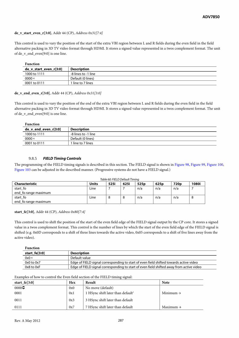
ADV7850
Rev. A May 2012 287
de_v_start_even_r[3:0], Addr 44 (CP), Address 0x31[7:4] This control is used to vary the position of the start of the extra VBI region between L and R fields during the even field in the field alternative packing in 3D TV video format through HDMI. It stores a signed value represented in a twos complement format. The unit of de_v_end_even[9:0] is one line.
Function de_v_start_even_r[3:0] Description 1000 to 1111 -8 lines to -1 line 0000 Default (0 lines) 0001 to 0111 1 line to 7 lines
de_v_end_even_r[3:0], Addr 44 (CP), Address 0x31[3:0] This control is used to vary the position of the end of the extra VBI region between L and R fields during the even field in the field alternative packing in 3D TV video format through HDMI. It stores a signed value represented in a twos complement format. The unit of de_v_end_even[9:0] is one line.
Function de_v_end_even_r[3:0] Description 1000 to 1111 -8 lines to -1 line 0000 Default (0 lines) 0001 to 0111 1 line to 7 lines
9.8.5 FIELD Timing Controls The programming of the FIELD timing signals is described in this section. The FIELD signal is shown in Figure 98, Figure 99, Figure 100, Figure 103 can be adjusted in the described manner. (Progressive systems do not have a FIELD signal.)
Table 60: FIELD Default Timing Characteristic Units 525i 625i 525p 625p 720p 1080i start_fo end_fo range maximum
Line 7 7 n/a n/a n/a 7
start_fo end_fo range maximum
Line 8 8 n/a n/a n/a 8
start_fe[3:0], Addr 44 (CP), Address 0x80[7:4] This control is used to shift the position of the start of the even field edge of the FIELD signal output by the CP core. It stores a signed value in a twos complement format. This control is the number of lines by which the start of the even field edge of the FIELD signal is shifted (e.g. 0x0D corresponds to a shift of three lines towards the active video, 0x05 corresponds to a shift of five lines away from the active video).
Function start_fe[3:0] Description 0x0 Default value 0x0 to 0x7 Edge of FIELD signal corresponding to start of even field shifted towards active video 0x8 to 0xF Edge of FIELD signal corresponding to start of even field shifted away from active video
Examples of how to control the Even field section of the FIELD timing signal: start_fe[3:0] Hex Result Note 0000 0x0 No move (default) 0001 0x1 1 HSync shift later than default1 Minimum →
0011 0x3 3 HSync shift later than default
0111 0x7 7 HSync shift later than default Maximum →
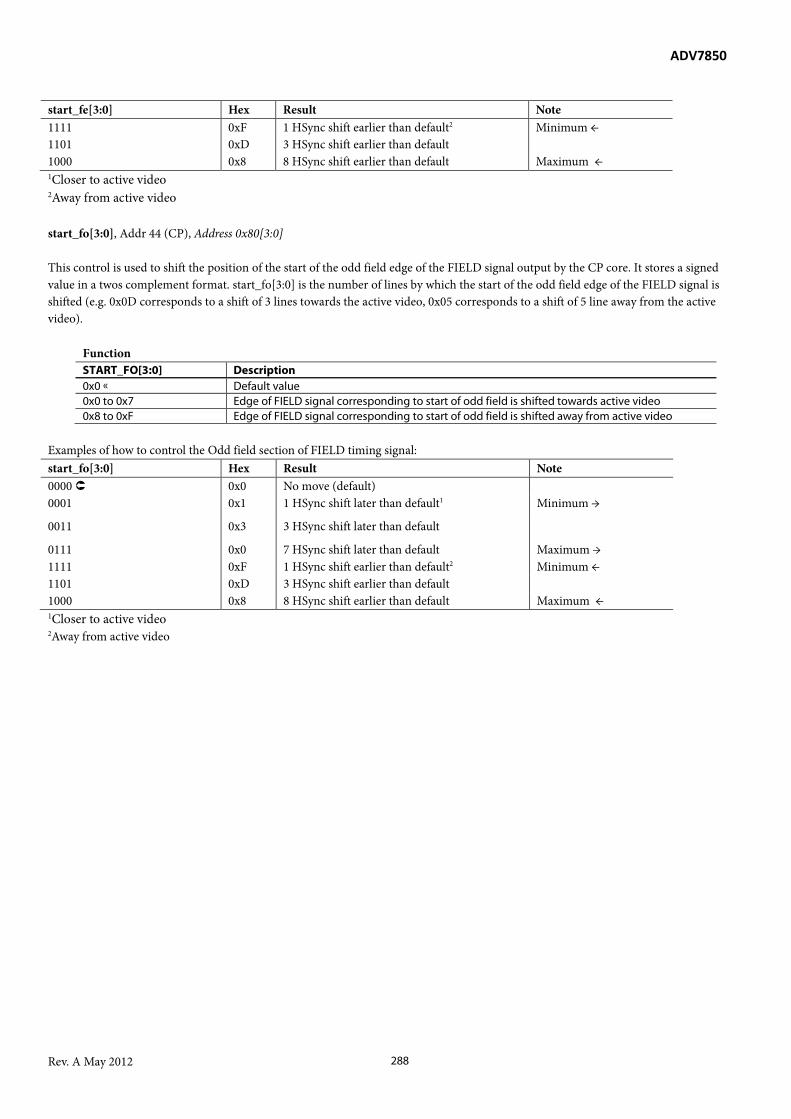
ADV7850
Rev. A May 2012 288
start_fe[3:0] Hex Result Note 1111 0xF 1 HSync shift earlier than default2 Minimum ← 1101 0xD 3 HSync shift earlier than default 1000 0x8 8 HSync shift earlier than default Maximum ← 1Closer to active video 2Away from active video start_fo[3:0], Addr 44 (CP), Address 0x80[3:0] This control is used to shift the position of the start of the odd field edge of the FIELD signal output by the CP core. It stores a signed value in a twos complement format. start_fo[3:0] is the number of lines by which the start of the odd field edge of the FIELD signal is shifted (e.g. 0x0D corresponds to a shift of 3 lines towards the active video, 0x05 corresponds to a shift of 5 line away from the active video).
Function START_FO[3:0] Description 0x0 Default value 0x0 to 0x7 Edge of FIELD signal corresponding to start of odd field is shifted towards active video 0x8 to 0xF Edge of FIELD signal corresponding to start of odd field is shifted away from active video
Examples of how to control the Odd field section of FIELD timing signal: start_fo[3:0] Hex Result Note 0000 0x0 No move (default) 0001 0x1 1 HSync shift later than default1 Minimum →
0011 0x3 3 HSync shift later than default
0111 0x0 7 HSync shift later than default Maximum → 1111 0xF 1 HSync shift earlier than default2 Minimum ← 1101 0xD 3 HSync shift earlier than default 1000 0x8 8 HSync shift earlier than default Maximum ← 1Closer to active video 2Away from active video

ADV7850
Rev. A May 2012 289
Figure 98: 525i VS Timing

ADV7850
Rev. A May 2012 290
Figure 99: 625i VS Timing

ADV7850
Rev. A May 2012 291
Figure 100: 525p VS Timing

ADV7850
Rev. A May 2012 292
Figure 101: 625p VS Timing

ADV7850
Rev. A May 2012 293
Figure 102: 720p VS Timing

ADV7850
Rev. A May 2012 294
Figure 103: 1080i VS Timing

ADV7850
Rev. A May 2012 295
Figure 104: 1080p VS Timing
15
67
8.....41
4242
Start_V
S [3:0]E
nd_VS
[3:0]
11211122
11252
31

ADV7850
Rev. A May 2012 296
9.8.6 HCOUNT Timing Control hcount_align_adj[4:0], Addr 44 (CP), Address 0xBE[1:0]; Address 0xBF[7:5] This control is used to manually adjust for internally generated hcount offset. The control allows an adjustment of 15 pixels to the left or to the right. The MSB sets the direction (left or right) and the four LSBs set the number of pixels to move.
Function hcount_align_adj[4:0] Description 00000 Default
9.9 CP DATA PROCESSING DELAY CONTROLS The ADV7850 provides controls to delay data by 1 pixel after CP CSC. dly_a, Addr 44 (CP), Address 0xBE[7] This control is used to delay the data on channel A by one pixel clock cycle.
Function dly_a Description 1 Delay data of channel A by one pixel clock cycle 0 Do not delay data of channel A
dly_b, Addr 44 (CP), Address 0xBE[6] This control is used to delay the data on channel B by one pixel clock cycle.
Function dly_b Description 1 Delay data of channel B by one pixel clock cycle 0 Do not delay data of channel B
dly_c, Addr 44 (CP), Address 0xBE[5] This control is used to delay the data on channel C by one pixel clock cycle.
Function dly_c Description 1 Delay data of channel C by one pixel clock cycle 0 Do not delay data of channel C
9.10 CP HORIZONTAL LOCK STATUS The ADV7850 provides an I2C readback value for the lock robustness. The measurement is based on an integration of the area of the horizontal synchronization that falls below the slicing threshold, as illustrated by Figure 105. The threshold level can be determined automatically or it can also be set by the customer via I2C. The quality of horizontal locking depends on the strength, that is, depth, of the horizontal synchronization pulse. For shallow horizontal synchronization pulses, the area measured is low and the locking is not as reliable as for a strong, deep, horizontal synchronization. The number presented as isd[8:0] is not intended to be an absolute measurement, but a relative one. A large value indicates robust locking and a small value shows an unreliable lock state. A system controller reading the ISD value via the IP
2C interface must set appropriate thresholds for fully locked and partially locked.

ADV7850
Rev. A May 2012 297
Figure 105: Synchronization Lock Robustness Measurement
The measurements are performed on a line-by-line basis on all video lines but not during the VBI. For video lines during the VBI, the result of the last active video line is kept. The isd[8:0] value changes dynamically on a line by line basis; the ifsd[8:0] is an averaged version of the isd[8:0]. The averaging length can be set to 128 or 256 lines of video. isd_thr[7:0], Addr 44 (CP), Address 0x83[7:0] This control is used to set the threshold used for the ISD measurement. Isd_thr[7:0] stores a 12-bit unsigned value.
Function isd_thr[7:0] Description 0x00 Calculate threshold automatically and set to (level of HSync tip) + 0.5 * (HSync depth) >0x01 Set threshold to (isd_thr[7:0] * 8)
ifsd_avg, Addr 44 (CP), Address 0x84[0] This control is used to set the averaging mode used to compute ifsd[8:0].
Function ifsd_avg Description 0 isd[8:0] averaged over 128 lines of video to generate ifsd[8:0] 1 isd[8:0] averaged over 256 lines of video to generate ifsd[8:0]
isd[8:0], Addr 44 (CP), Address 0xE3[0]; Address 0xE4[7:0] (Read Only) This readback represents the area of the HSync that falls below the slicing threshold set by isd_thr[7:0]. A high value indicates robust locking.
Function isd[8:0] Description xxxxxxxxx Readback value
ifsd[8:0], Addr 44 (CP), Address 0xE3[1]; Address 0xE5[7:0] (Read Only) This readback displays the average value of the ISD measurement over 128 or 256 lines. The number of lines used to compute ifsd[8:0] is set in ifsd_avg.
Function ifsd[8:0] Description xxxxxxxxx Readback value
video signal
HS detection thresholdas per ISD_THR[7:0]
ISD[8:0] value representsarea value

ADV7850
Rev. A May 2012 298
9.11 NOISE AND CALIBRATION The ADV7850 provides hardware for a noise and calibration measurements. The two measurements share some hardware control (window). However, they are different in the way they examine the input data. The measurements are executed during a time window. The window can be positioned anywhere within a line of video and the length can be selected to be 16, 32, 64, or 128 LLC clock cycles. Notes:
• Both measurements are performed on the channel A. • Both measurements work on a video line basis and are performed during the active video. • The tap-off point for both measurements is right after the gain multiplier. Clamping and AGC/manual gain will affect the
numbers reported back.
9.11.1 Measurement Window The window for the noise and calibration measurements is set via meas_ws[11:0] and meas_wl[1:0]. meas_ws[11:0], Addr 44 (CP), Address 0x81[3:0]; Address 0x82[7:0] This control is used to set the start value of the measurement window use for noise and calibration. The unit is a pixel clock cycle. Refer to noise[7:0] and calib[10:0]. A value of 0 positions the start of the window at the trailing edge of the incoming HSync.
Function meas_ws[11:0] Description 0x000 Start value (in LLC clock cycles) of measurement window 0x004 Default
meas_wl[1:0], Addr 44 (CP), Address 0x81[7:6] This control is used to set the width of the window length used for noise calibration measurements. The unit is a pixel clock cycle. Refer to noise[7:0] and calib[10:0].
Function meas_wl[1:0] Description 00 Window length of 128 LLC clock cycles 01 Window length of 64 LLC clock cycles 10 Window length of 32 LLC clock cycles 11 Window length of 16 LLC clock cycles
9.11.2 Noise Measurement For the noise or peak data measurement, the data during the window is monitored for the maximum and the minimum value. After the window is closed, the difference between the two is presented. If programmed during a quiet time of the input video, the value presented can be related back to the level of noise within the video signal. The noise level is presented as an unsigned number. Levels greater than 255 are saturated to 255. noise[7:0], Addr 44 (CP), Address 0xE2[7:0] (Read Only) This readback displays the noise value measured on the luma channel (i.e. channel A). It provides an unsigned value representing the difference between the maximum and minimum value measured during the window configured by meas_ws[11:0] and meas_wl[1:0].
Function noise[7:0] Description xxxxxxxx Readback value

ADV7850
Rev. A May 2012 299
9.11.3 Calibration Measurement The input signal is accumulated during the measurement window. After the end of the window, the accumulated value is divided by the window length and the result (average signal level over the extent of the window) is presented via the I2C register CALIB[10:0]. The number format is signed with a possible range of -1024 to +1024. It is envisaged to provide the ADV7850 with a flat gray field and to position the window in the middle of active video for a meaningful measurement. calib[10:0], Addr 44 (CP), Address 0xE3[4:2]; Address 0xE6[7:0] (Read Only) This readback displays the calibration value measured on the luma channel (i.e. channel A). It provides a signed value representing the average level over the extent of the window configured by meas_ws[11:0] and meas_wl[1:0].
Function calib[10:0] Description xxxxxxxxxxx Readback value
Note: The calibration measurement can be negative as the samples used for this measurement are taken before the offset block of the A channel. The data is signed before the offset block and unsigned after the offset block.
9.12 FREE RUN MODE Free run mode provides the user with a stable clock and predictable data if the input signal cannot be decoded, for example, if input video is not present. It controls default color insertion and causes the ADV7850 to generate a default clock. The state in which this happens can be monitored via the cp_free_run status bit. (Refer to Section 9.13 for more information.) The free run feature is configured automatically for analog modes. The free run feature must be configured for HDMI modes.
9.12.1 Free Run Mode Thresholds The free run threshold parameters define the horizontal and vertical conditions under which free run mode is entered. The horizontal and vertical parameters of the incoming video signal are measured and compared with internally stored parameters, and the magnitude of the difference decides whether or not to enter free run. The internally stored parameters are decoded by default from prim_mode[3:0] and vid_std[5:0]. For video standards other than the preprogrammed settings of prim_mode[3:0] and vid_std[5:0], the parameters can be set manually.
9.12.1.1 Horizontal Free Run Conditions The horizontal conditions are based on the length of the incoming video line, which is measured based on the 27 MHz crystal clock. This value is compared with the internally stored horizontal parameter, the ideal line length. ch1_f_run_th[2:0] and ch2_f_run_th[2:0] allow the user to select the threshold for channel 1 and channel 2 respectively. The ideal line length can be manually set via the Free-run Line Length controls, ch1_fr_ll[10:0] and ch2_fr_ll[10:0]. ch1_f_run_thr[2:0], Addr 44 (CP), Address 0xF3[2:0] This control is used to select the free run threshold for sync channel 1. It determines the horizontal conditions under which free run mode is entered or left. The length of the incoming video line is measured based on the crystal clock and is compared to an internally stored parameter. The magnitude of the difference decides whether or not sync channel 1 will enter free run mode.

ADV7850
Rev. A May 2012 300
Function ch1_f_run_thr[2:0] Description 000 Minimum difference to switch into free run is 2. Maximum difference to switch out of free run
is 1. 001 Minimum difference to switch into free run is 256. Maximum difference to switch out of free
run is 200. 010 Minimum difference to switch into free run is 128. Maximum difference to switch out of free
run is 112. 011 Minimum difference to switch into free run is 64. Maximum difference to switch out of free
run is 48. 100 Minimum difference to switch into free run is 32. Maximum difference to switch out of free
run is 24. 101 Minimum difference to switch into free run is 16. Maximum difference to switch out of free
run is 12. 110 Minimum difference to switch into free run is 8. Maximum difference to switch out of free run
is 6. 111 Minimum difference to switch into free run is 4. Maximum difference to switch out of free run
is 3. ch2_f_run_thr[2:0], Addr 44 (CP), Address 0x43[2:0] This control is used to select the free run threshold for sync channel 2. It determines the horizontal conditions under which free run mode is entered or left. The length of the incoming video line is measured based on the crystal clock and compared to an internally stored parameter. The magnitude of the difference decides whether or not sync channel 2 will enter free run mode.
Function ch2_f_run_thr[2:0] Description 000 Minimum difference to switch into free run is 2. Maximum difference to switch out of free run
is 1. 001 Minimum difference to switch into free run is 256. Maximum difference to switch out of free
run is 200. 010 Minimum difference to switch into free run is 128. Maximum difference to switch out of free
run is 112. 011 Minimum difference to switch into free run is 64. Maximum difference to switch out of free
run is 48. 100 Minimum difference to switch into free run is 32. Maximum difference to switch out of free
run is 24. 101 Minimum difference to switch into free run is 16. Maximum difference to switch out of free
run is 12. 110 Minimum difference to switch into free run is 8. Maximum difference to switch out of free run
is 6. 111 Minimum difference to switch into free run is 4. Maximum difference to switch out of free run
is 3. ch1_fr_ll[10:0], Addr 44 (CP), Address 0x8F[2:0]; Address 0x90[7:0] This control is used to set the free run line length in a number of crystal clock cycles in one line of video for sync channel 1 STDI. It should be programmed only with video standards that are not supported by prim_mode[3:0] and vid_std[5:0].
Function ch1_fr_ll[10:0] Description 0x000 Internal free run line length decoded from prim_mode[3:0] and vid_std[5:0]. All other values Number of crystal clocks in ideal line length. Used to enter or exit free run mode.
ch2_fr_ll[10:0], Addr 44 (CP), Address 0x47[2:0]; Address 0x48[7:0] This control is used to define the free run line length in the number of crystal clock cycles in one line of video for sync channel 2 STDI. This control should only be programmed for video standards that are not supported by prim_mode[3:0] and vid_std[5:0].

ADV7850
Rev. A May 2012 301
Function ch2_fr_ll[10:0] Description 0x000 Actually used internal free run line length decoded from prim_mode[3:0] and vid_std[5:0]. All other values Number of crystal clocks in ideal line length. Used to enter or exit free run mode.
Notes:
• This parameter has no effect on the video decoding. • If neither ch1_fr_ll[10:0] nor ch2_fr_ll[10:0] are programmed, then the Free-run Line Length parameter is decoded from
prim_mode[3:0] and vid_std[5:0]. • If ch1_fr_ll[10:0] is programmed and ch2_fr_ll[10:0] is not, the Free-run Line Length parameter defined by ch1_fr_ll[10:0] is
used for both channels.
9.12.2 Vertical Run Conditions In the case of the vertical conditions, the number of lines per field of incoming video signal is measured. This value is compared with an internally stored vertical parameter, the ideal field length. ch1_fl_fr_threshold[1:0] and ch2_fl_fr_threSHOLD[1:0] allow the user to select the threshold for channel 1 and channel 2 respectively. The ideal number of lines per field can be set manually via cp_lcount_max[11:0]. ch1_fl_fr_threshold[2:0], Addr 44 (CP), Address 0xF3[5:3] This readback indicates the threshold for the difference between the input video field length and the internally stored standard to enter and exit free run.
Function ch1_fl_fr_threshold[2:0] Description 000 Minimum difference to switch into free run is 36 lines. Maximum difference to switch out of
free run is 31 lines. 001 Minimum difference to switch into free run is 18 lines. Maximum difference to switch out of
free run is 15 lines. 010 Minimum difference to switch into free run is 10 lines. Maximum difference to switch out of
free run is 7 lines. 011 Minimum difference to switch into free run is 4 lines. Maximum difference to switch out of free
run is 3 lines. 100 Minimum difference to switch into free run is 51 lines. Maximum difference to switch out of
free run is 46 lines. 101 Minimum difference to switch into free run is 69 lines. Maximum difference to switch out of
free run is 63 lines. 110 Minimum difference to switch into free run is 134 lines. Maximum difference to switch out of
free run is 127 lines. 111 Minimum difference to switch into free run is 263 lines. Maximum difference to switch out of
free run is 255 lines.
ch2_fl_fr_threshold[2:0], Addr 44 (CP), Address 0x43[5:3] This control is used to define the threshold of the difference between the input video field length and the internally stored standard to enter and exit free run. It is used for the sync channel 2 STDI.

ADV7850
Rev. A May 2012 302
Function ch2_fl_fr_threshold[2:0] Description 000 Minimum difference to switch into free run is 36 lines. Maximum difference to switch out of
free run is 31 lines. 001 Minimum difference to switch into free run is 18 lines. Maximum difference to switch out of
free run is 15 lines. 010 Minimum difference to switch into free run is 10 lines. Maximum difference to switch out of
free run is 7 lines. 011 Minimum difference to switch into free run is 4 lines. Maximum difference to switch out of free
run is 3 lines. 100 Minimum difference to switch into free run is 51 lines. Maximum difference to switch out of
free run is 46 lines. 101 Minimum difference to switch into free run is 69 lines. Maximum difference to switch out of
free run is 63 lines. 110 Minimum difference to switch into free run is 134 lines. Maximum difference to switch out of
free run is 127 lines. 111 Minimum difference to switch into free run is 263 lines. Maximum difference to switch out of
free run is 255 lines. cp_lcount_max[11:0], Addr 44 (CP), Address 0xAB[7:0]; Address 0xAC[7:4] This control is used to set a manual value for the total number of lines in a frame expected by the CP core. This control is used for the manual configuration of the free run feature. The value programmed here is used for sync channel 1 and is also used for sync channel 2 if ch2_fr_field_length[10:0] is set to 0x000. It is an unsigned value.
Function cp_lcount_max[11:0] Description 0x000 Ideal number of lines per frame decoded from prim_mode[3:0] and vid_std[5:0] for sync
channel 1 All other values Use programmed value as ideal number of lines per frame in free run decision for sync
channel 1 interlaced, Addr 44 (CP), Address 0x91[6] This control is used to set the interlaced or progressive mode of the incoming video processed in CP mode.
Function interlaced Description 0 CP core expects video mode is progressive 1 CP core expects video mode is interlaced
Field Line Count is the vertical parameter that holds the ideal number of lines per field for a given video standard. It affects the way CP handles the unlocked state. If cp_lcount_max[11:0] and ch2_fr_field_length[10:0] are set to 0, the internally used free run line length value is decoded from the current setting of prim_mode[3:0] and vid_std[5:0]. For standards not covered by the preprogrammed values, the cp_lcount_max[11:0], ch2_fr_field_length[10:0], and interlaced parameters must be set to the ideally expected number of lines per field. Notes:
• cp_lcount_max[11:0] has no effect on the video decoding. • If neither cp_lcount_max[11:0] nor ch2_fr_field_length[10:0] are programmed, then the Free-run Line Length parameter is
decoded from prim_mode[3:0] and vid_std[5:0]. • If cp_lcount_max[11:0] is programmed and ch2_fr_field_length[10:0] is not, the Free-run Line Length parameter defined by
cp_lcount_max[11:0] and interlaced is used for both channel 1 and channel 2. • If cp_lcount_max[11:0] is programmed and ch2_fr_field_length[10:0] is also programmed, the Free-run Line Length parameter
defined by cp_lcount_max[11:0] and interlaced is used for channel 1. The Free-run Line Length parameter defined by ch2_fr_field_length[10:0] is used for channel 2.

ADV7850
Rev. A May 2012 303
ch2_fr_field_length[11:0], Addr 44 (CP), Address 0x46[7:0]; Address 0x47[7:4] This code is used to define the ideal number of lines per field used by the CP core for the free run decision for sync channel 2. If set to 0, the ideal number of lines per field is dictated by cp_lcount_max[11:0].
Function ch2_fr_field_length[11:0]
Description
0x000 Default
Figure 106: Free Run Field Length Selection for Channel 1 and Channel 2
9.12.3 Free Run Default Color Output In the event of loss of input signal, the ADV7850 may enter free run and can be configured to output a color rather than noise. By default, the ADV7850 is configured to output a blue screen. The default color values are provided in Table 61. The times at which the default colors are inserted can be set as follows:
• Free run is forced: default colors are always output • Automatic free run mode: default colors are output when the system detects a loss of video signal
Table 61: Default Color Output Values (CP)
Mode cp_def_col_man_val Signal Value
Default – GR 0 CH_A (G) 0 CH_B (R) 0 CH_C (B) 135d
Default – COMP 0 CH_A (Y) 35d
CH_A (Pr) 114d
CH_A (Pb) 212d
Man. Override 1 CH_A 4·DEF_COL_CHA[7:0] CH_B 4·DEF_COL_CHB[7:0] CH_C 4·DEF_COL_CHC[7:0]
cp_force_freerun, Addr 44 (CP), Address 0xBF[0] This control is used to force the CP to free run.
Function cp_force_freerun Description 0 Do not force CP core free run 1 Force CP core to free run
Lcount_MaxBased on PM/VS
CP_LCOUNT_MAX[11:0]0
0
0
1
1
1
[11:0]
CP_LCOUNT_MAX[11:0]== 12'd0
[11:1]
[10:0]
[10:0]
INTERLACED
FR_FIELD_LENGTH Used On Sync Channel 1
FR_FIELD_LENGTH Used On Sync Channel 2
CH2_FR_FIELD_LENGTH == 11’d0
CH2_FR_FIELD_LENGTH[10:0]
ADV7850
Rev. A May 2012 304
cp_def_col_auto, Addr 44 (CP), Address 0xBF[1] This control is used to enable the insertion of the default color when the CP free runs.
Function cp_def_col_auto Description 0 Disable automatic insertion of default color 1 Output default colors when CP free runs
cp_def_col_man_val, Addr 44 (CP), Address 0xBF[2] This control is used to enable the manual selection of the color used when the CP core free runs.
Function cp_def_col_man_val Description 0 Use default color blue 1 Output default colors as given in cp_def_col_cha, cp_def_col_chb and cp_def_col_chc
Table 61 shows the default colors for component and graphics based video. The values describe the color blue. By setting cp_def_col_man_val to 1, the user can overwrite the default colors with the values given in def_col_cha[7:0], def_col_chb[7:0], and def_col_chc[7:0]. The def_col_cha[7:0], def_col_chb[7:0], and def_col_chc[7:0] controls allow users to specify their own default values. Note: cp_def_col_man_val must be set to 1 for these three controls to be used. See Table 61 for more information on the automatic values. def_col_cha[7:0], Addr 44 (CP), Address 0xC0[7:0] This control is used to set the default color for channel A. It is used if cp_def_col_man_val is set at 1.
Function def_col_cha[7:0] Description 0x00 Default
def_col_chb[7:0], Addr 44 (CP), Address 0xC1[7:0] This control is used to set the default color for channel B. It is used if cp_def_col_man_val is set at 1.
Function def_col_chb[7:0] Description 0x00 Default
def_col_chc[7:0], Addr 44 (CP), Address 0xC2[7:0] This control is used to set the default color for channel C. It is used if cp_def_col_man_val is set at 1.
Function def_col_chc[7:0] Description 0x00 Default
9.13 CP STATUS cp_reg_ff is a status register that contains status bits for the CP core. The cp_reg_ff register holds the following fields: mv_ps_det, mv_agc_det, and cp_free_run.
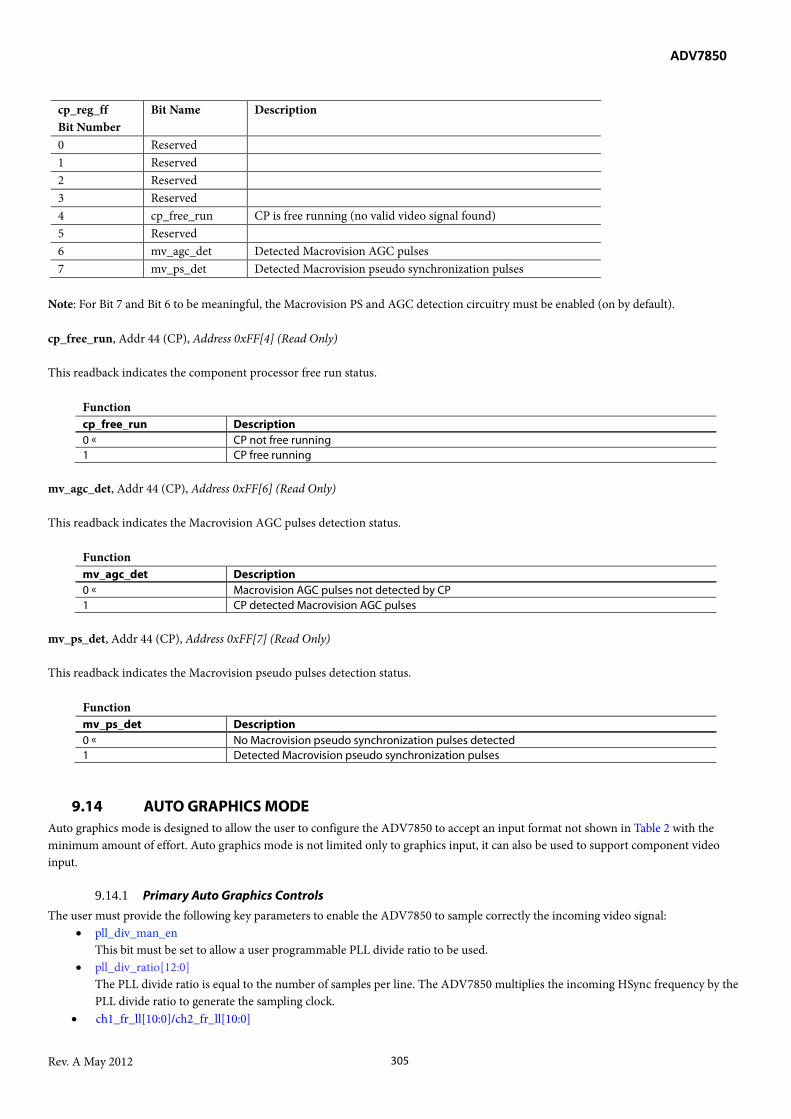
ADV7850
Rev. A May 2012 305
cp_reg_ff Bit Number
Bit Name Description
0 Reserved 1 Reserved 2 Reserved 3 Reserved 4 cp_free_run CP is free running (no valid video signal found) 5 Reserved 6 mv_agc_det Detected Macrovision AGC pulses 7 mv_ps_det Detected Macrovision pseudo synchronization pulses
Note: For Bit 7 and Bit 6 to be meaningful, the Macrovision PS and AGC detection circuitry must be enabled (on by default). cp_free_run, Addr 44 (CP), Address 0xFF[4] (Read Only) This readback indicates the component processor free run status.
Function cp_free_run Description 0 CP not free running 1 CP free running
mv_agc_det, Addr 44 (CP), Address 0xFF[6] (Read Only) This readback indicates the Macrovision AGC pulses detection status.
Function mv_agc_det Description 0 Macrovision AGC pulses not detected by CP 1 CP detected Macrovision AGC pulses
mv_ps_det, Addr 44 (CP), Address 0xFF[7] (Read Only) This readback indicates the Macrovision pseudo pulses detection status.
Function mv_ps_det Description 0 No Macrovision pseudo synchronization pulses detected 1 Detected Macrovision pseudo synchronization pulses
9.14 AUTO GRAPHICS MODE Auto graphics mode is designed to allow the user to configure the ADV7850 to accept an input format not shown in Table 2 with the minimum amount of effort. Auto graphics mode is not limited only to graphics input, it can also be used to support component video input.
9.14.1 Primary Auto Graphics Controls The user must provide the following key parameters to enable the ADV7850 to sample correctly the incoming video signal:
• pll_div_man_en This bit must be set to allow a user programmable PLL divide ratio to be used.
• pll_div_ratio[12:0] The PLL divide ratio is equal to the number of samples per line. The ADV7850 multiplies the incoming HSync frequency by the PLL divide ratio to generate the sampling clock.
• ch1_fr_ll[10:0]/ch2_fr_ll[10:0]

ADV7850
Rev. A May 2012 306
ch1_fr_ll[10:0]/ch2_fr_ll[10:0] specifies the expected line length of the incoming video. If the actual line length is different from the expected line length by more than a programmable threshold, the decoder will free run.
• cp_lcount_max[11:0]/ch2_fr_field_length[11:0] / interlaced cp_lcount_max[11:0] and ch2_fr_field_length[11:0] specify the expected number of lines per frame. If the actual number of lines per frame is different from the expected number by more than a programmable threshold, the decoder will free run. interlaced should be set to 1 if the processed video is interlaced and set to 0 otherwise.
pll_div_man_en, Addr A0 (VFE), Address 0x16[7] This control is used to manually override the PLL divider ratio value.
Function pll_div_man_en Description 0 << Disable manual PLL divider ratio settings. PLL divider ratio set by prim_mode[3:0] and
vid_std[5:0]. 1 Set pll_div ratio manually as defined by pll_div[12:0].
cp_start_vbi[11:0], Addr 44 (CP), Address 0xA5[7:0]; Address 0xA6[7:4] This control is used to set the manual value for the start of the VBI region position (of odd fields in case of interlaced output). This is an unsigned value. It sets the total number of lines at the start of a frame of non interlaced standard video. Programming is optional and should only be performed when the part is set in autographics mode.
Function cp_start_vbi[11:0] Description 0x000 Default
cp_end_vbi[11:0], Addr 44 (CP), Address 0xA6[3:0]; Address 0xA7[7:0] This control is used to set a manual value for the end of the VBI region position (of odd fields in the case of interlaced output). It an unsigned value. It sets the total number of lines at the end of a frame of noninterlaced standard video. It sets the total number of lines at the end of the odd frame of interlaced standard video. Programming is optional and should only be performed when the part is set in autographics mode.
Function cp_end_vbi[11:0] Description 0x000 Default
cp_start_vbi_even[11:0], Addr 44 (CP), Address 0xA8[7:0]; Address 0xA9[7:4] This control is used to set a manual value for the start of the VBI in even fields. It an unsigned value. It sets the total number of lines at the start of the even frame of interlaced standard. Programming is optional and should only be performed when the part is set in autographics mode.
Function cp_start_vbi_even[11:0] Description 0x000 Default
cp_end_vbi_even[11:0], Addr 44 (CP), Address 0xA9[3:0]; Address 0xAA[7:0] This control is used to set a manual value for the end of the VBI in even fields. It is an unsigned value. It sets the total number of lines at the end of the even frame of interlaced standard. Programming is optional and should only be performed when the part is set in autographics mode.

ADV7850
Rev. A May 2012 307
Function cp_end_vbi_even[11:0] Description 0x000 << Default value
The following controls are intended only for use with HDMI 3D standards. cp_start_vbi_r[11:0], Addr 44 (CP), Address 0x2A[7:0]; Address 0x2B[7:4] This control is used to manually set the value for the start position of the VBI region. This is the extra blank region preceding the odd right (R) field in the 3D TV field alternative packing format supported by HDMI. It is not required to set this value. In normal operation, this parameter is automatically calculated from the input. cp_end_vbi_r[11:0], Addr 44 (CP), Address 0x2B[3:0]; Address 0x2C[7:0] This control is used to manually set the value for the end of VBI position. This is the extra blank region preceding the odd right field in the 3D TV field alternative packing format supported by HDMI. It is not required to set this value. In normal operation, this parameter is automatically calculated from the input. cp_start_vbi_even_r[11:0], Addr 44 (CP), Address 0x2D[7:0]; Address 0x2E[7:4] This control is used to manually set the value for the start position of the VBI region. This is the extra blank region preceding the even right field in the 3D TV field alternative packing format supported by HDMI. It is not required to set this value. In normal operation, this parameter is automatically calculated from the input. cp_end_vbi_even[11:0], Addr 44 (CP), Address 0xA9[3:0]; Address 0xAA[7:0] This control is used to set the manual value for the end of the VBI region position for even fields. It is an unsigned value. It sets the total number of lines at the end of the even frame of interlaced standard. Programming is optional and should only be performed when the part is set in autographics mode.
Function cp_end_vbi_even[11:0] Description 0x000 Default
It is also possible to adjust the position of the HSync and VSync signals. The following controls to adjust these are signed numbers to allow adjustment in either direction from the current position:
• cp_start_hs[12:0] • cp_end_hs[12:0] • cp_start_vs[5:0] • cp_end_vs[5:0] • cp_start_vs_even[10:0] • cp_end_vs_even[10:0]
cp_start_hs[12:0], Addr 44 (CP), Address 0x22[4:0]; Address 0x23[7:0] This control is used to set the position of the start of the HSync output signal in the CP core in autographic mode only. Programming of this control is optional and should only be performed when the part is set in autographics mode. The value is unsigned.
Function cp_start_hs[12:0] Description 0x0000 Default

ADV7850
Rev. A May 2012 308
cp_end_hs[12:0], Addr 44 (CP), Address 0x24[4:0]; Address 0x25[7:0] This control is used to set the position of the end of the HSync output signal in the CP core in autographics mode only. Programming of this control is optional and should only be performed when the part is set in autographics mode. The value is unsigned.
Function cp_end_hs[12:0] Description 0x0000 Default
cp_start_vs[5:0], Addr 44 (CP), Address 0x9A[5:0] This control is used to set the position of the start of the VSync output signal in the CP core in autographics mode only. In the case of an interlaced signal, this control adjusts the odd VS signal. Programming of this control is optional and should only be performed when the part is set in autographics mode. The value is unsigned.
Function cp_start_vs[5:0] Description 000000 Default
cp_end_vs[5:0], Addr 44 (CP), Address 0x9B[5:0] This control is used to set the position of the end of the VSync output signal in the CP core in autographics mode only. In the case of an interlaced signal, this control adjusts the odd VS signal. Programming of this control is optional and should only be performed when the part is set in autographics mode. The value is unsigned.
Function cp_end_vs[5:0] Description 000000 Default
cp_start_vs_even[10:0], Addr 44 (CP), Address 0x9C[6:0]; Address 0x9D[7:4] This control is used to set the position of the start of the even VSync output signal in the CP core in autographics mode only. Programming of this control is optional and should only be performed when the part is set in autographic mode. The value is unsigned.
Function cp_start_vs_even[10:0] Description 0x000 Default
cp_end_vs_even[10:0], Addr 44 (CP), Address 0x9D[2:0]; Address 0x9E[7:0] This control is used to set the position of the end of the even VSync output signal in the CP core in autographic mode only. Programming of this control is optional and should only be performed when the part is set in autographic mode. The value is unsigned.
Function cp_end_vs_even[10:0] Description 0x000 Default
9.14.2 Graphics Controls This section describes the auxiliary controls available for the auto graphic controls. It is recommended to leave these controls at the default.

ADV7850
Rev. A May 2012 309
ignr_clmp_vs_mar_start[4:0], Addr 44 (CP), Address 0x8A[0]; Address 0x8B[7:4] This control is used to set the start of the window during which the clamp is ignored. It stores the unsigned number of pixel clocks between the start position of the window relative to the leading edge of the VSync. This control should only be used if vid_std[5:0] is set for autographics mode.
Function ignr_clmp_vs_mar_start[4:0]
Description
0x04 Default ignr_clmp_vs_mar_end[4:0], Addr 44 (CP), Address 0x8A[7:3] This control is used to set the end of the window during which the clamp is ignored. It stores the unsigned number of pixel clocks between the end position of the window relative to the trailing edge of the VSync. This control should only be used if vid_std[5:0] is set for autographics mode.
Function ignr_clmp_vs_mar_end[4:0]
Description
0x04 Default auto_sl_filter_freeze_en, Addr 44 (CP), Address 0xCB[5] This control is used to determine if the internally generated parameter for the position of the HSync trailing edge is updated during the VBI region. It is intended only for autographics mode. It is recommended to leave it at the default, otherwise the part may generate an incorrect HSync trailing edge position parameter if the input synchronization is embedded and has serration pulses.
Function auto_sl_filter_freeze_en
Description
0 Do not freeze trailing edge position of HSync during VBI region 1 Freeze trailing edge position of HSync during VBI region
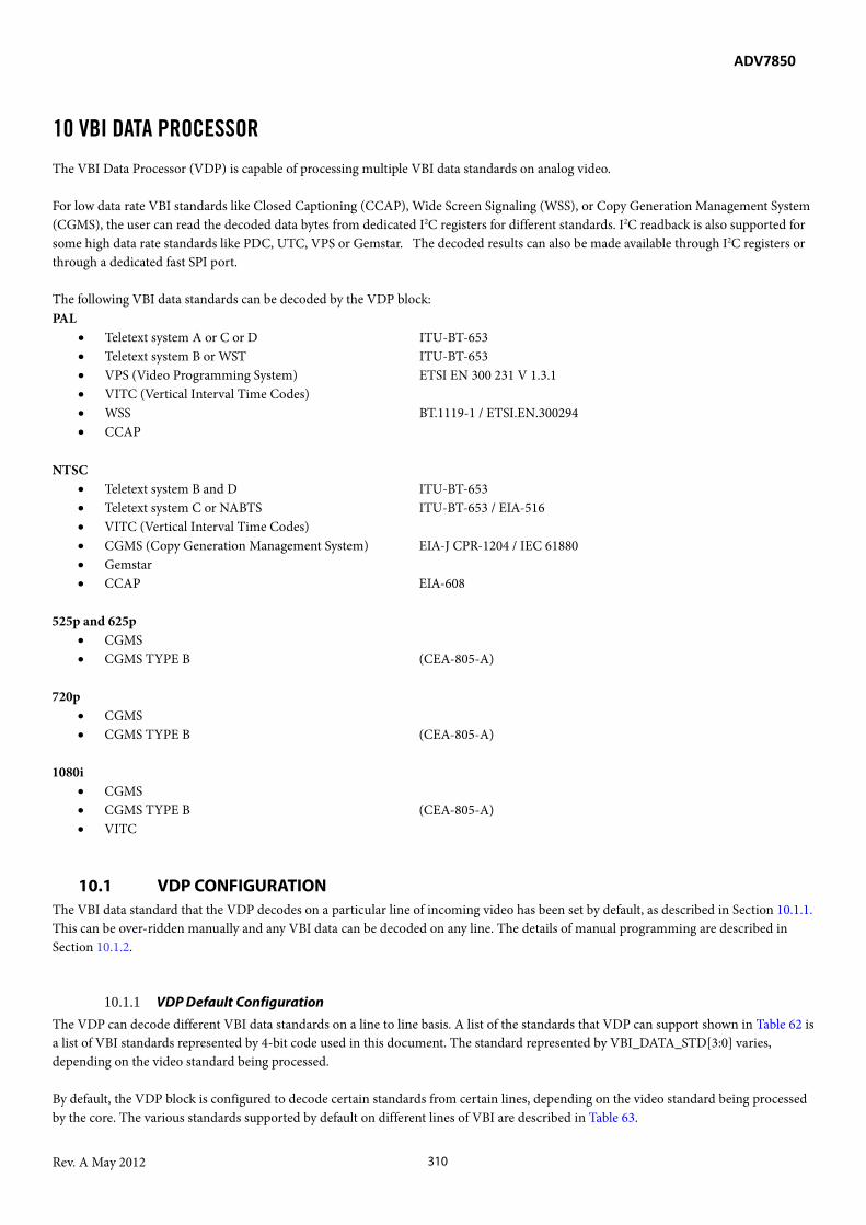
ADV7850
Rev. A May 2012 310
10 VBI DATA PROCESSOR
The VBI Data Processor (VDP) is capable of processing multiple VBI data standards on analog video. For low data rate VBI standards like Closed Captioning (CCAP), Wide Screen Signaling (WSS), or Copy Generation Management System (CGMS), the user can read the decoded data bytes from dedicated I2C registers for different standards. I2C readback is also supported for some high data rate standards like PDC, UTC, VPS or Gemstar. The decoded results can also be made available through I2C registers or through a dedicated fast SPI port. The following VBI data standards can be decoded by the VDP block: PAL
• Teletext system A or C or D ITU-BT-653 • Teletext system B or WST ITU-BT-653 • VPS (Video Programming System) ETSI EN 300 231 V 1.3.1 • VITC (Vertical Interval Time Codes) • WSS BT.1119-1 / ETSI.EN.300294 • CCAP
NTSC
• Teletext system B and D ITU-BT-653 • Teletext system C or NABTS ITU-BT-653 / EIA-516 • VITC (Vertical Interval Time Codes) • CGMS (Copy Generation Management System) EIA-J CPR-1204 / IEC 61880 • Gemstar • CCAP EIA-608
525p and 625p
• CGMS • CGMS TYPE B (CEA-805-A)
720p
• CGMS • CGMS TYPE B (CEA-805-A)
1080i
• CGMS • CGMS TYPE B (CEA-805-A) • VITC
10.1 VDP CONFIGURATION The VBI data standard that the VDP decodes on a particular line of incoming video has been set by default, as described in Section 10.1.1. This can be over-ridden manually and any VBI data can be decoded on any line. The details of manual programming are described in Section 10.1.2.
10.1.1 VDP Default Configuration The VDP can decode different VBI data standards on a line to line basis. A list of the standards that VDP can support shown in Table 62 is a list of VBI standards represented by 4-bit code used in this document. The standard represented by VBI_DATA_STD[3:0] varies, depending on the video standard being processed. By default, the VDP block is configured to decode certain standards from certain lines, depending on the video standard being processed by the core. The various standards supported by default on different lines of VBI are described in Table 63.

ADV7850
Rev. A May 2012 311
Table 62: vbi_data_std[3:0] Values Corresponding to a Particular VBI Standard
vbi_data_std[3:0] 625/50 – PAL (Interlaced)
525/60 – NTSC (Interlaced)
525p 625p 720p 1080i
Binary Dec
0001 1 Teletext system1 Teletext system1 Reserved Reserved Reserved Reserved 0010 2 VPS2 Reserved Reserved Reserved Reserved Reserved 0011 3 VITC VITC Reserved Reserved Reserved VITC 0100 4 WSS3 CGMS4 CGMS4 CGMS4 CGMS4 CGMS4 0101 5 Reserved GEMSTAR_1X Reserved Reserved Reserved Reserved 0110 6 Reserved GEMSTAR_2X Reserved Reserved Reserved Reserved 0111 7 CCAP5 CCAP 5 Reserved Reserved Reserved Reserved 1000 8 Reserved Reserved CGMS B6 Reserved CGMS B6 CGMS B6 1001 9 Reserved Reserved Reserved Reserved Reserved Reserved 1010 10 Reserved Reserved Reserved Reserved Reserved Reserved 1011 11 Reserved Reserved Reserved Reserved Reserved Reserved 1100 12 Reserved Reserved Reserved Reserved Reserved Reserved 1101 13 Reserved Reserved Reserved Reserved Reserved Reserved 1110 14 Reserved Reserved Reserved Reserved Reserved Reserved 1111 15 Disable VDP - - - - -
Refer to Table 62 to interpret a standard represented by vbi_data_std (as decoded VBI standard depends on video standard 525i/625i/525p etc.)
Table 63: Default Standards on Lines for Supported Interlaced and Progressive Standards 525i 625i 525p 625p 720p 1080i Line No.
Default vbi_data_std [3:0]
Line No.
Default vbi_data_std [3:0]
Line No.
Default vbi_data_std [3:0]
Line No.
default vbi_data_std [3:0]
Line No.
Default vbi_data_std [3:0]
Line No.
Default vbi_data_std [3:0]
6 1 6 - 6 - 6 - 6 - 7 1 7 - 7 - 7 - 7 - 8 1 8 - 8 - 8 - 8 - 9 1 9 - 9 - 9 - 9 3 10 1 10 1 10 - 10 - 10 - 10 - 11 1 11 1 11 - 11 - 11 - 11 - 12 1 12 1 12 - 12 - 12 - 12 - 13 1 13 1 13 - 13 - 13 - 13 - 14 3 14 1 14 - 14 - 14 - 14 - 15 1 15 1 15 - 15 - 15 - 15 - 16 1 16 2 16 - 16 - 16 - 16 - 17 1 17 1 17 - 17 - 17 - 17 - 18 1 18 1 18 - 18 - 18 - 18 - 19 1 19 3 19 - 19 - 19 - 19 4 20 4 20 1 20 - 20 - 20 - 20 - 21 7 21 1 21 - 21 - 21 - 21 - 22 1 22 7 22 - 22 - 22 - 23 6 23 4 23 - 23 - 23 - 24 6 24 0 24 - 24 - 24 4 25 6 - - 25 - 25 - 25 - 272 1 318 2 26 - 26 - 26 - 569 - 273 1 319 1 27 - 27 - 27 - 570 -
1 Teletext system identified by vdp_ttxt_type 2 VPS – ETSI EN 300 231 V 1.3.1 3 WSS BT.1119-1/ ETSI.EN.300294 4 CGMS EIA-J CPR-1204 / IEC 61880 5 CCAP EIA-608 6 CGMS TYPE B (CEA-805-A)

ADV7850
Rev. A May 2012 312
525i 625i 525p 625p 720p 1080i Line No.
Default vbi_data_std [3:0]
Line No.
Default vbi_data_std [3:0]
Line No.
Default vbi_data_std [3:0]
Line No.
default vbi_data_std [3:0]
Line No.
Default vbi_data_std [3:0]
Line No.
Default vbi_data_std [3:0]
274 1 320 1 28 - 28 - 28 - 571 3 275 1 321 1 29 - 29 - 29 - 572 - 276 1 322 1 30 - 30 - 30 - 573 - 277 3 323 1 31 - 31 - 31 - 574 - 278 1 324 1 32 - 32 - 32 - 575 - 279 1 325 1 33 - 33 - 33 - 576 - 280 1 326 1 34 - 34 - 34 - 577 - 281 1 327 1 35 - 35 - 35 - 578 - 282 1 328 1 36 - 36 - 36 - 579 - 283 4 329 2 37 - 37 - 37 - 580 - 284 7 330 1 38 - 38 - 38 - 581 - 285 1 331 1 39 - 39 - 39 - 582 4 286 6 332 3 40 - 40 - 40 - 583 - 287 6 333 1 41 4 41 - 41 - 584 - 288 6 334 1 42 - 42 - 42 - 335 7 43 - 43 4 43 - 336 1 44 - 44 - 44 - 337 0 45 - 45 - 45 -
10.1.2 VDP Manual Configuration Table 63 shows default standards decoded by the VDP. However decoded standard(s) on specific line(s) can be manually reconfigured by using Manual Line Programming registers (refer to Table 64). To select a standard decoded on a particular line, write the desired VBI standard code to a register corresponding to that specific line (vdp_man_line_x_y). VBI standard codes (vbi_data_std) are 4-bit codes defined in Table 62. For example: To decode a VITC on line number 15 in 525i: Write 0b0011 (VITC – see Table 62) to a vdp_man_line_10_30[7:4] A zero value in the Manual Line Programming register means that the default VBI standard for that line will be decoded (as in Table 63).
Table 64: Details of Manual Line Programming Registers
Control Names Register Location
Line Numbers in which VBI Data is Inserted 525i 625i 1080i
525p, 625p, 720p
vdp_man_line_1_21[7:4] 0x64 6 6 6 vdp_man_line_2_22[7:4] 0x65 7 7 7 vdp_man_line_3_23[7:4] 0x66 8 8 8 vdp_man_line_4_24[7:4] 0x67 9 9 9 vdp_man_line_5_25[7:4] 0x68 10 10 10 10 vdp_man_line_6_26[7:4] 0x69 11 11 11 11 vdp_man_line_7_27[7:4] 0x6A 12 12 12 12 vdp_man_line_8_28[7:4] 0x6B 13 13 13 13 vdp_man_line_9_29[7:4] 0x6C 14 14 14 14 vdp_man_line_10_30[7:4] 0x6D 15 15 15 15 vdp_man_line_11_31[7:4] 0x6E 16 16 16 16 vdp_man_line_12_32[7:4] 0x6F 17 17 17 17 vdp_man_line_13_33[7:4] 0x70 18 18 18 18 vdp_man_line_14_34[7:4] 0x71 19 19 19 19 vdp_man_line_15_35[7:4] 0x72 20 20 20 20
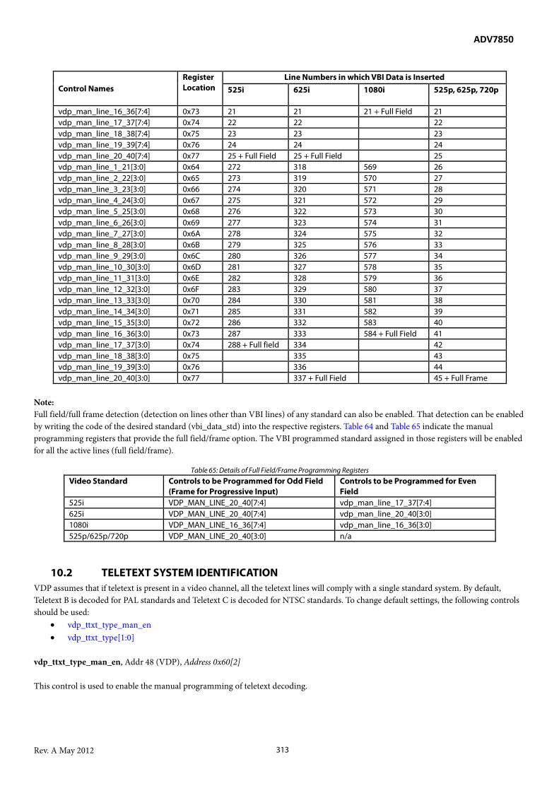
ADV7850
Rev. A May 2012 313
Control Names Register Location
Line Numbers in which VBI Data is Inserted 525i 625i 1080i
525p, 625p, 720p
vdp_man_line_16_36[7:4] 0x73 21 21 21 + Full Field 21 vdp_man_line_17_37[7:4] 0x74 22 22 22 vdp_man_line_18_38[7:4] 0x75 23 23 23 vdp_man_line_19_39[7:4] 0x76 24 24 24 vdp_man_line_20_40[7:4] 0x77 25 + Full Field 25 + Full Field 25 vdp_man_line_1_21[3:0] 0x64 272 318 569 26 vdp_man_line_2_22[3:0] 0x65 273 319 570 27 vdp_man_line_3_23[3:0] 0x66 274 320 571 28 vdp_man_line_4_24[3:0] 0x67 275 321 572 29 vdp_man_line_5_25[3:0] 0x68 276 322 573 30 vdp_man_line_6_26[3:0] 0x69 277 323 574 31 vdp_man_line_7_27[3:0] 0x6A 278 324 575 32 vdp_man_line_8_28[3:0] 0x6B 279 325 576 33 vdp_man_line_9_29[3:0] 0x6C 280 326 577 34 vdp_man_line_10_30[3:0] 0x6D 281 327 578 35 vdp_man_line_11_31[3:0] 0x6E 282 328 579 36 vdp_man_line_12_32[3:0] 0x6F 283 329 580 37 vdp_man_line_13_33[3:0] 0x70 284 330 581 38 vdp_man_line_14_34[3:0] 0x71 285 331 582 39 vdp_man_line_15_35[3:0] 0x72 286 332 583 40 vdp_man_line_16_36[3:0] 0x73 287 333 584 + Full Field 41 vdp_man_line_17_37[3:0] 0x74 288 + Full field 334 42 vdp_man_line_18_38[3:0] 0x75 335 43 vdp_man_line_19_39[3:0] 0x76 336 44 vdp_man_line_20_40[3:0] 0x77 337 + Full Field 45 + Full Frame
Note: Full field/full frame detection (detection on lines other than VBI lines) of any standard can also be enabled. That detection can be enabled by writing the code of the desired standard (vbi_data_std) into the respective registers. Table 64 and Table 65 indicate the manual programming registers that provide the full field/frame option. The VBI programmed standard assigned in those registers will be enabled for all the active lines (full field/frame).
Table 65: Details of Full Field/Frame Programming Registers Video Standard Controls to be Programmed for Odd Field
(Frame for Progressive Input) Controls to be Programmed for Even Field
525i VDP_MAN_LINE_20_40[7:4] vdp_man_line_17_37[7:4] 625i VDP_MAN_LINE_20_40[7:4] vdp_man_line_20_40[3:0] 1080i VDP_MAN_LINE_16_36[7:4] vdp_man_line_16_36[3:0] 525p/625p/720p VDP_MAN_LINE_20_40[3:0] n/a
10.2 TELETEXT SYSTEM IDENTIFICATION VDP assumes that if teletext is present in a video channel, all the teletext lines will comply with a single standard system. By default, Teletext B is decoded for PAL standards and Teletext C is decoded for NTSC standards. To change default settings, the following controls should be used:
• vdp_ttxt_type_man_en • vdp_ttxt_type[1:0]
vdp_ttxt_type_man_en, Addr 48 (VDP), Address 0x60[2] This control is used to enable the manual programming of teletext decoding.

ADV7850
Rev. A May 2012 314
Function vdp_ttxt_type_man_en Description 0 Manual programming of teletext disabled 1 Manual programming of teletext enabled
vdp_ttxt_type[1:0], Addr 48 (VDP), Address 0x60[1:0] This readback indicates the teletext type detected. It is functional only if vdp_ttxt_type_man_en is set to 1.
Function vdp_ttxt_type[1:0] Description 00 ITU_BT.653-625/50-A - for PAL 01 ITU_BT.653-625/50-B(WST) - for PAL; ITU_BT.653-525/60-B - for NTSC 10 ITU_BT.653-625/50-C(WST) - for PAL; ITU_BT.653-525/60-C or EIA516(NABTS) - for NTSC 11 ITU_BT.653-625/50-D - for PAL; ITU_BT.653-525/60-D -
10.3 VDP DECODED DATA READBACK REGISTERS
10.3.1 Teletext Readback Registers Since teletext is a high data rate standard, decoded bytes are provided via ancillary data. A status bit is provided to indicate the teletext detection status. vdp_status_ttxt, Addr 48 (VDP), Address 0x40[7] (Read Only) This readback displays the teletext detection status.
Function vdp_status_ttxt Description 0 Teletext not detected 1 Teletext detected
10.3.2 CGMS and WSS Readback Registers CGMS and WSS convey the same type of information for different video standards. WSS is a 625i standard while CGMS is a 525i, 525p, 625p, 720p, and 1080i standard. Hence, the CGMS and WSS readback registers are shared. WSS is biphase coded and the VDP does a biphase decoding to produce the 14 raw WSS bits to be available in the CGMS and WSS VDP readback registers. A status bit is set when this data is available. status_clear_wss_cgms, Addr 48 (VDP), Address 0x78[2] (Self-Clearing) This control is used to refresh the WSS and CGMS readback registers. This is a self-clearing bit.
Function status_clear_wss_cgms Description 0 Do not refresh WSS and CGMS readback registers 1 Refresh WSS and CGMS readback registers
vdp_status_wss_cgms, Addr 48 (VDP), Address 0x40[2] (Read Only) This readback displays the WSS or CGMS type A data detection status.

ADV7850
Rev. A May 2012 315
Function vdp_status_wss_cgms Description 0 WSS or CGMS type A data not detected 1 WSS or CGMS type A data detected
vdp_cgms_wss_data[23:0], Addr 48 (VDP), Address 0x43[7:0]; Address 0x44[7:0]; Address 0x45[7:0] (Read Only) This readback displays decoded data for CGMS type A and WSS.
Function vdp_cgms_wss_data[23:0]
Description
vdp_cgms_wss_data[23:0]
decoded CGMS[23:0] data
vdp_cgms_wss_data[13:0]
decoded WSS[13:0] data
Figure 107: WSS (625i) Waveform
Figure 108: CGMS (525i) Waveform
10.3.3 Closed Captioning Readback Registers Two bytes of decoded closed caption (CCAP) data are made available in the VDP readback registers. The vdp_status_ccap_even_field identifies the field from which the CCAP data was decoded. status_clear_ccap, Addr 48 (VDP), Address 0x78[0] (Self-Clearing) This control is used to refresh the CCAP status registers. This is a self-clearing bit.
Function status_clear_ccap Description 0 Do not refresh CCAP status registers 1 Refresh CCAP status registers

ADV7850
Rev. A May 2012 316
vdp_status_ccap, Addr 48 (VDP), Address 0x40[0] (Read Only) This readback displays the closed caption data detection status.
Function vdp_status_ccap Description 0 Closed caption data not detected 1 Closed caption data detected
vdp_status_ccap_even_field, Addr 48 (VDP), Address 0x40[1] (Read Only) This readback displays the closed caption data in the even field status.
Function vdp_status_ccap_even_field
Description
0 Closed caption data not detected in even field 1 Closed caption data detected in even field
vdp_ccap_data[15:8], Addr 48 (VDP), Address 0x42[7:0] (Read Only) This readback displays byte 2 of the decoded closed caption data.
Function vdp_ccap_data[15:8] Description xxxxxxxx Byte 2 of decoded closed caption data
Figure 109: CCAP Waveform and Decoded Data Correlation
10.3.4 VITC Readback Registers The decoded VITC data bytes are available in the vdp_vitc_data registers (refer to Table 66). The VDP also calculates a CRC for the decoded data bytes and is made available in the vdp_vitc_calc_crc control.

ADV7850
Rev. A May 2012 317
status_clear_vitc, Addr 48 (VDP), Address 0x78[6] (Self-Clearing) This control is used to refresh the VITC status registers. This is a self-clearing bit.
Function status_clear_vitc Description 0 Do not refresh VITC status registers 1 Refresh VITC status registers
vdp_vitc_calc_crc[7:0], Addr 48 (VDP), Address 0x5E[7:0] (Read Only) This readback indicates the calculated CRC value for decoded VITC data.
Function vdp_vitc_calc_crc[7:0] Description xxxxxxxx Readback value
vdp_vitc_data[71:0], Addr 48 (VDP), Address 0x5D[7:0]; Address 0x5C[7:0]; Address 0x5B[7:0]; Address 0x5A[7:0]; Address 0x59[7:0]; Address 0x58[7:0]; Address 0x57[7:0]; Address 0x56[7:0]; Address 0x55[7:0] (Read Only) This readback displays decoded VITC data.
Table 66: VITC Readback Registers VITC Data Bits Address in VDP Map
VITC bits [9:2] 0x55[7:0] VITC bits [19:12] 0x56[7:0] VITC bits [29:22] 0x57[7:0] VITC bits [39:32] 0x58[7:0] VITC bits [49:42] 0x59[7:0] VITC bits [59:52] 0x5A[7:0] VITC bits [69:62] 0x5B[7:0] VITC bits [79:72] 0x5C[7:0] VITC bits [89:82] 0x5D[7:0] VITC CRC 0x5E[7:0]
Figure 110: VITC Waveform and Decoded Data Correlation
10.3.5 VPS, PDC, UTC, Gemstar and CGMS Type B Readback Registers The readback registers for VPS, PDC, and UTC are shared. Since Gemstar is a high data rate standard, it is available through the ancillary stream and the fast I2C interface. However, for evaluation purposes, any one line of Gemstar is available through readback registers sharing the same register space as PDC, UTC, and VPS. Note that only one standard out of VPS, PDC, UTC, and Gemstar can be read back through the registers at a time. To identify the data that should be made available in the readback registers, the user has to program gs_vps_pdc_utc_cgmstb[2:0].

ADV7850
Rev. A May 2012 318
gs_vps_pdc_utc_cgmstb[2:0], Addr 48 (VDP), Address 0x9C[2:0] The readback registers for VPS, PDC, UTC and CGMS type B are shared. This control is used to identify which type of data is to be written to the shared registers.
Function gs_vps_pdc_utc_cgmstb[2:0]
Description
000 Gemstar 1x/2x 001 VPS 010 PDC 011 UTC 100 CGMS type B 101 Reserved 110 Reserved 111 Reserved
status_clear_gems_vps, Addr 48 (VDP), Address 0x78[4] (Self-Clearing) This control is used to refresh the Gemstar and VPS status registers. This is a self-clearing bit.
Function status_clear_gems_vps Description 0 Do not refresh VPS status registers 1 Refresh VPS readback registers
vdp_status_gs_vps_pdc_utc_cgmstb, Addr 48 (VDP), Address 0x40[4] (Read Only) This readback displays the Gemstar, VPS, PDC, UTC, and CGMS type B data detection status.
Function vdp_status_gs_vps_pdc_utc_cgmstb
Description
0 Gemstar, VPS, PDC, UTC, and CGMS type B data not detected 1 Gemstar, VPS, PDC, UTC, and CGMS type B data detected
Table 67: vdp_gs_vps_pdc_utc_cgmstb_data Readback Registers
GS PDC UTC Readback Registers VDP Map/SDP Map
Address
vdp_gs_vps_pdc_utc_cgmstb_data[7:0] 0x47 vdp_gs_vps_pdc_utc_cgmstb_data[15:8] 0x48 vdp_gs_vps_pdc_utc_cgmstb_data[23:16] 0x49 vdp_gs_vps_pdc_utc_cgmstb_data[31:24] 0x4A vdp_gs_vps_pdc_utc_cgmstb_data[39:32] 0x4B vdp_gs_vps_pdc_utc_cgmstb_data[47:40] 0x4C vdp_gs_vps_pdc_utc_cgmstb_data[55:48] 0x4D vdp_gs_vps_pdc_utc_cgmstb_data[63:56] 0x4E vdp_gs_vps_pdc_utc_cgmstb_data[71:64] 0x4F vdp_gs_vps_pdc_utc_cgmstb_data[79:72] 0x50 vdp_gs_vps_pdc_utc_cgmstb_data[87:80] 0x51 vdp_gs_vps_pdc_utc_cgmstb_data[95:88] 0x52 vdp_gs_vps_pdc_utc_cgmstb_data[103:96] 0x53
VPS The VPS data bits are biphase decoded by the VDP. The decoded data is made available in both the ancillary stream and in the VDP readback registers. VPS decoded data is available in the vdp_gs_vps_pdc_utc_cgmstb_data registers (refer to Table 67).

ADV7850
Rev. A May 2012 319
Gemstar The Gemstar decoded data is made available in the ancillary stream and through the fast I2C port. For evaluation purposes only one line of Gemstar can be made available VDP readback registers. Gemstar must be selected via gs_vps_pdc_utc_cgmstb[2:0]. VDP supports the autodetection of the Gemstar standard between Gemstar 1x or Gemstar 2x formats, and decodes accordingly. This autodetection feature must be enabled via the auto_detect_gem bit and program the decoder to decode Gemstar 2x on the required lines through manual configuration of the VDP. The type of decoded Gemstar can be found out by observing the vdp_status_gems_type bit. auto_detect_gem, Addr 48 (VDP), Address 0x61[4] This control is used for the autodetection of the Gemstar type.
Function auto_detect_gem Description 0 Disable autodetection of Gemstar type 1 Enable autodetection of Gemstar type
vdp_status_gems_type, Addr 48 (VDP), Address 0x40[5] (Read Only) This readback displays the Gemstar type.
Function vdp_status_gems_type Description 0 Gemstar 1X detected 1 Gemstar 2X detected
The Gemstar data that is available in the VDP readback register could be from any line of the input video on which Gemstar was decoded. If the user wants to read the Gemstar data on a particular video line, the user should use the manual configuration described in Section 10.1.2 and enable Gemstar decoding on only the required line. PDC and UTC PDC and UTC are data transmitted through teletext packet 8/30 format 2; and packet 8/30 format 1. If PDC or UTC data is to be read through VDP readback registers, the corresponding teletext standard (WST – PAL System B) should be decoded by VDP. The whole teletext decoded packet is output on the ancillary data stream and the user can look for the magazine number, row number, and 319designation code, and qualify the data as PDC/UTC. If PDC/UTC packets are identified by the VDP, bytes 0 to 12 are updated to the vdp_gs_vps_pdc_utc_cgmstb_data registers (refer to Table 68), and vdp_status_gems_vps is set accordingly. The full packet data is also available as ancillary data. CGMS Type B The CGMS Type B data can be present in 525p, 720p, and 1080i standards. The CGMS Type B standard has a total of 134 bits (16 bytes, 6 bits). The decoded data is made available in both the ancillary stream and in the VDP readback registers. The CGMS Type B data is made available in VDP readback registers in a shared manner. The first four bytes are available in dedicated registers and the remaining bytes are available in registers in the share registers of vdp_gs_vps_pdc_utc_cgmstb_data.
Table 68: CGMS Type B Readback Registers CGMS Type B Readback Registers VDP Map Address vdp_cgms_typeb_0 0x3C vdp_cgms_typeb_1 0x3D vdp_cgms_typeb_2 0x3E vdp_cgms_typeb_3 0x3F vdp_gs_vps_pdc_utc_cgmstb_data[7:0] 0x47 vdp_gs_vps_pdc_utc_cgmstb_data[15:8] 0x48 vdp_gs_vps_pdc_utc_cgmstb_data[23:16] 0x49

ADV7850
Rev. A May 2012 320
CGMS Type B Readback Registers VDP Map Address vdp_gs_vps_pdc_utc_cgmstb_data[31:24] 0x4A vdp_gs_vps_pdc_utc_cgmstb_data[39:32] 0x4B vdp_gs_vps_pdc_utc_cgmstb_data[47:40] 0x4C vdp_gs_vps_pdc_utc_cgmstb_data[55:48] 0x4D vdp_gs_vps_pdc_utc_cgmstb_data[63:56] 0x4E vdp_gs_vps_pdc_utc_cgmstb_data[71:64] 0x4F vdp_gs_vps_pdc_utc_cgmstb_data[79:72] 0x50 vdp_gs_vps_pdc_utc_cgmstb_data[87:80] 0x51 vdp_gs_vps_pdc_utc_cgmstb_data[95:88] 0x52 vdp_gs_vps_pdc_utc_cgmstb_data[103:96] 0x53
10.4 READBACK REGISTERS I2C readback registers have separate registers for CCAP, CGMS, WSS, Gemstar, VPS, PDC/UTC, and VITC. The details of these registers and their access procedure are described in Section 10.5.
10.5 USER INTERFACE FOR I2C READBACK REGISTERS VDP supports two types of I2C interfaces for the readback of decoded data:
• Dedicated I2C registers (normal I2C bus) • Shared I2C (fast I2C bus)
Dedicated I2C readback registers have separate registers for CCAP, CGMS, WSS, GEMSTAR, VPS, PDC/UTC, and VITC, whereas the fast I2C space has a shared space of 45 registers that can be used for any or a combination of VBI data standards. The details of these registers and their access procedure are described in this section.
10.5.1 VDP Register Readback Protocols
10.5.1.1 Data Available Updates
The VDP decodes all enabled VBI data standards in real time. Since the I2C access speed is much lower than the decoded rate, it is possible that when the registers are accessed, they are updated with data from the next line. In order to avoid this, the VDP block has a clear control bit and an available status bit accompanying all the VDP readback registers. Initially, the user has to clear the I2C readback register by writing 1 to the clear bit (this control is self clearing). This resets the state of the available bit to low and indicates that the data in the associated readback registers are not valid. After the VDP decodes the next line of the corresponding VBI data, the decoded data is placed in the I2C readback register and the available bit is set to high to indicate that valid data is now available. Though the VDP will decode this VBI data, if present, in subsequent lines, the decoded data will not be updated to the readback registers until the CLEAR bit is set HIGH again. However, this data will be available through the 656 ancillary data packets. Example I2C Readback Procedure: The following tasks are performed to read one packet (line) of PDC data from the decoder.
1. Write ‘10’ to gs_vps_pdc_utc_cgmstb[2:0] to specify that PDC data has to be updated to I2C registers. 2. Set status_clear_gems_vps to 1 to enable the update of I2C registers. 3. Poll the vdp_status_gs_vps_pdc_utc_cgmstb / gs_pdc_vps_utc_avl_st bit going high to check the availability of the PDC
packets. 4. Read the data bytes from the PDC I2C registers. 5. Repeat steps 1 to 4 to read another line or packet of data. 6. To read a packet of CC, CGMS, or WSS, steps 2, 3, and 4 only are required since they have dedicated registers.

ADV7850
Rev. A May 2012 321
10.5.2 Content Based Data Update For certain standards like WSS, CGMS, Gemstar, PDC, UTC, and VPS, the information content in the transmitted signal remains the same over numerous lines but the user may want to be notified only when there is a change in the information content or loss of the information content. The user needs to enable the content based update for the required standard through the gs_vps_pdc_utc_cb_change and wss_cgms_cb_change bits. Thus, the available bit will show the availability of that standard only when there is a change in its content. Available bits are located in the vdp_status control. The content based update also applies to loss of data at the lines where some data was present previously. For standards like VPS, Gemstar, CGMS, and WSS, if there is no data arrival in the next four lines programmed, the corresponding available bit in the vdp_status register is set to 1 and the content in the readback registers for that standard is set to 0. The user has to write high to the clear bit so that if a valid line is decoded after some time so that the readback registers will be updated with the available bit set to 1. If content based updating is enabled, the available bit is set to high (assuming the clear bit was written) in the following cases:
• Data contents change • There was some data being decoded and four lines with no data are detected • There was no data being decoded and new data is being decoded
gs_vps_pdc_utc_cb_change, Addr 48 (VDP), Address 0x9C[5] This control is used to allow content based updates of VPS, PDC and UTC data.
Function gs_vps_pdc_utc_cb_change
Description
0 Disable content based update of VPS, PDC, UTC data 1 Enable content based update of UTC, PDC, UTC data
wss_cgms_cb_change, Addr 48 (VDP), Address 0x9C[4] This control is used to allow content based updates of WSS and CGMS type A data.
Function wss_cgms_cb_change Description 0 Disable content based update of WSS and CGMS type A data 1 Enable content based update of WSS and CGMS type A data
The VDP_STATUS register (VDP Map, 0x40) consists of the following bits:
• vdp_status_ttxt • vdp_status_gems_type • vdp_status_gs_vps_pdc_utc_cgmstb • vdp_status_ccap_even_field • vdp_status_ccap
10.6 INTERRUPT BASED READING OF VDP READBACK REGISTERS Some VDP status bits are also linked to the interrupt request controller so that the user does not have to poll the Available status bit. The user can configure the video decoder to trigger an interrupt request on an interrupt pin in response to the valid data available in the readback registers. This function is available for the CGMS, WSS, Gemstar, PDC, VPS and UTC data types. The user can select between triggering an interrupt request each time sliced data is available or triggering an interrupt request only when the sliced data has changed. For more information on using the VDP interrupts, refer to Section 15 and the ADV7850 Software Manual.

ADV7850
Rev. A May 2012 322
10.7 SPI READBACK REGISTERS For all VBI data standards, the user can read back the decoded data on lines through the SPI interface. Users can select the standard(s) they want to read through the SPI registers. A FIFO is used in the VDP to facilitate storage of decoded data while data is being read through the SPI interface. The data in FIFO is arranged in the following order:
• Type of standard (VBI_DATA_STD) • Number of data bytes that follow (packet size) • Decoded data bytes
After setting the required bits, the user can read back the decoded data from the registers addressed 0xC4 to 0xF0 in the VDP Map. The first two bytes of the registers let the user know the type of standard for which the data is available and the number of data bytes to be read. Table 69 explains the bits to be set for different VBI data that are available through the fast I2C registers.
Table 69: Configuration VBI Standard to be Output on SPI Interface vdp_fast_reg_ conf_cus , VDP Map 0xC0[7]
vdp_fast_reg_ conf_cust, VDP Map 0xC0[6]
vdp_fast_reg_ conf_ccap, VDP Map 0xC0[5]
vdp_fast_reg_conf_gem1x_2x, VDP Map 0xC0[4]
vdp_fast_reg_conf_cgms_ wss, VDP Map 0xC0[3]
vdp_fast_reg_ conf_vitc, VDP Map 0xC0[2]
vdp_fast_reg_conf_vps_cgmstb, VDP Map 0xC0[1]
vdp_fast_ reg_conf_ ttxt, VDP Map 0xC0[0]
Description
0 0 0 0 0 0 0 0 None (default)
0 0 0 0 0 0 0 1 Teletext 0 0 0 0 0 0 1 0 VPS 0 0 0 0 0 1 0 0 VITC 0 0 0 0 1 0 0 0 CGMS/WSS 0 0 0 1 0 0 0 0 Gemstar
1x/2x 0 0 1 0 0 0 0 0 CCAP 0 1 0 0 0 0 0 0 Custom
Mode1 1 0 0 0 0 0 0 0 Custom
Mode2
10.7.1 SPI Data Formats – Slave Mode The ADV7850 will always be configured in SPI master mode when transferring to the ADV8003. However, the ADV7850 can also output VBI data over SPI in slave mode. The format of these packets is shown in Table 70 to Table 75.
Table 70: Standard SPI Slave Mode Output Format
Byte No. Contents Description 0 0x00 Dummy byte 1 XX Number of bytes in this block 2 YY VBI standard and field information 3 ZZ Framing Code 4 ZZ Framing Code 5 ZZ Framing Code 6 xx VBI Data N 7 xx VBI Data N-1 xx xx VBI Data 2 xx VBI Data 1 0xFD More data in FIFO XX Number of bytes in this block YY VBI standard and field information Framing Code

ADV7850
Rev. A May 2012 323
Two bytes are sent that are not transmitted when the ADV7850 SPI Tx is in master mode. These are the dummy byte and the byte indicating more data in the FIFO. More data in FIFO: Because of being in slave mode, the ADV7850 must indicate to the master that there is more data to read. Hence, it transmits:
• 0xFD: More data in FIFO
• 0x0D: No more data in FIFO
Table 71 to Table 75 show the composition of the SPI slave data format for a number of VBI standards.
Table 71: Teletext SPI Slave Mode Output Format
Byte No. Contents Description 0 0x00 Dummy byte 1 0x2F Number of bytes in this block (=47) 2 0xY1 VBI standard and field information 3 0x27 Framing Code 4 0x00 Framing Code 5 0x00 Framing Code 6 xx VBI Data 42 … xx VBI Data 2 xx VBI Data 1 0xFD More data in FIFO 0x2F Number of bytes in this block xx VBI standard and field information 0x27 Framing Code
Table 72: CCAP SPI Slave Mode Output Format
Byte No. Contents Description 0 0x00 Dummy byte 1 0x07 Number of bytes in this block (=7) 2 0xY7 VBI standard and field information 3 0x80 Framing Code 4 0x00 Framing Code 5 0x00 Framing Code 6 xx VBI Data 2 7 xx VBI Data 1 8 0x0D No more data in FIFO
Table 73: WSS SPI Slave Mode Output Format
Byte No. Contents Description 0 0x00 Dummy byte 1 0x07 Number of bytes in this block (=7) 2 0xY4 VBI standard and field information 3 0xF8 Framing Code 4 0x3C Framing Code 5 0x78 Framing Code 6 xx VBI Data 2 7 xx VBI Data 1 8 0x0D No more data in FIFO

ADV7850
Rev. A May 2012 324
Table 74: CGMS-A SPI Slave Mode Output Format Byte No. Contents Description 0 0x00 Dummy byte 1 0x08 Number of bytes in this block (=8) 2 0xY4 VBI standard and field information 3 0x00 Framing Code 4 0x00 Framing Code 5 0x00 Framing Code 6 xx VBI Data 3 7 xx VBI Data 2 8 xx VBI Data 1 9 0x0D No more data in FIFO
Table 75: CGMS-B SPI Slave Mode Output Format
Byte No. Contents Description 0 0x00 Dummy byte 1 0x15 Number of bytes in this block (=21) 2 0xY8 VBI standard and field information 3 0x00 Framing Code 4 0x00 Framing Code 5 0x00 Framing Code 6 xx VBI Data 16 xx VBI Data 2 xx VBI Data 1 23 0x0D No more data in FIFO
10.7.2 SPI Data Formats – Master Mode In master mode, the ADV7850 outputs the data according to the ancillary data packet format. The format for ancillary data packets is shown in Table 76 (considering 8-bit (byte) ancillary data only).
Table 76: Format of Ancillary Packets
D7 D6 D5 D4 D3 D2 D1 D0
Ancillary Data Preamble 0 0 0 0 0 0 0 0 1 1 1 1 1 1 1 1 1 1 1 1 1 1 1 1
Data ID (DID) 𝐷6 Even parity
- DID[4:0]
Secondary DID (SDID) 𝐷6 Even parity
SDID[5:0]
Data Count (DC) 𝐷6 Even parity
0 Data Count[4:0]
ID0 – user data word 0 𝐷6 Even parity
1 0 VBI Data Standard[3:0]
ID1 – user data word 1 𝐷6 Even parity
LCount[11:6]
ID2 – user data word 2 𝐷6 Even parity
LCount[5:0]
ID3 – user data word 3 𝐷6 Even parity
0 0 0 EF VDP Type[1:0]
User Data Word 4 VBI Word 1[7:0]
: :
: :

ADV7850
Rev. A May 2012 325
D7 D6 D5 D4 D3 D2 D1 D0 User Data Word N-1 VBI Word N-1[7:0] Padding 1 0 0 0 0 0 0 0 Padding 1 0 0 0 0 0 0 0 Checksum 𝐷6 Checksum
Ancillary packet data is composed of the following:
• Ancillary Data Preamble: First 3 bytes are the ancillary data preamble which indicates the start of a data packet. It will always be 0x00, 0xFF, 0xFF. The FF is a condition that cannot exist outside the preamble and the user data words. This is because D7 and D6 are an exclusive OR pair, in that when one is high, the other must be low. D6 is generally chosen to be an even parity bit, which is high if the number of 1’s in D5:D0 is odd and low if the number of 1’s in D5:D0 is even. D7 is then always NOT D6, ensuring that the all one and all zero condition cannot occur.
• Data ID (DID): Indicates the type of data being sent. • Secondary DID (SDID): Supplements the data ID for type 2 ancillary formats. • Data Count (DC): Indicates that number of user data words in the packet. • LCount: Advises the line from which this particular data packet was extracted. • Even Field (EF): Indicates the field from which the packet was decoded. • Checksum: Word used to increase the confidence in the integrity of the ancillary data packet. It is calculated by summing the 7
LSBs of all bytes from Data ID to User Data Word N-1. The 7 LSBs of this summation is the checksum, with the MSB being the NOT of the D6.
• VBI Data Standard: VBI data standard that should be decoded on each line of an incoming video is set by default. This can be over-ridden manually and any VBI data can be decoded from any line. Four bits are used in the ancillary packet to indicate which type of VBI data is encoded in the packet. (Refer to Table 62 for details.)
The first three VBI words are the framing codes (total of 24 bits). Some of the values used are shown in Table 77. Three bytes are used for each of the standards, but the framing codes for these standards may be less. Hence, the No. of Bits column indicates how many bits are used by the framing code for that standard in practice.
Table 77: Number of Bits in Each of Framing Codes
VBI Standard Framing Code No. of Bits CCAP (525i & 625i) 0x80, 0x00, 0x00 3 WSS (625i) 0xF8, 0x3C, 0x78 24 CGMS-A (525i, 525p, 720p, 1080i) 0x00, 0x00, 0x00 CGMS-B 0x00, 0x00, 0x00 Teletext System A 0xE7, 0x00, 0x00 8 Teletext System B 0x27, 0x00, 0x00 8 Teletext System C 0x27, 0x00, 0x00 8 Teletext System D 0xE7, 0x00, 0x00 8 VPS 0x99, 0x51, 0x00 16 VITC 0x00, 0x00, 0x00 1 GEMSTAR_1X 0x80, 0x00, 0x00 3 GEMSTAR_2X: 0xB7, 0x20, 0x00 1
These are then followed by the VBI data. The typical numbers of user data words are shown in Table 78.
Table 78: Number of Data Words in Ancillary Data Packet for Some VBI Standards
Standard No. of User data Words
No. of Framing Codes
No. of VBI Data Words
No. of Padding Words Sum
CCAP 4 3 2 3 12 WSS 4 3 2 3 12 CGMS-A 4 3 3 2 12 CGMS-B 4 3 17 0 24

ADV7850
Rev. A May 2012 326
Table 79: VBI Standard Number and Line Numbers for Each VBI Type
VBI Data Standard
525i 625i 525p 625p 720p 1080i
0 Auto Mode VDP 1 Teletext
(Lines: 10:12, 15:19, 22, 272:276, 278:282, 285)
Teletext (Lines: 6:15, 17, 18, 20, 22, 319:328, 330, 331, 333, 335, 336)
Reserved Reserved Reserved Reserved
2 Reserved VPS (Lines: 16, 318, 329)
Reserved Reserved Reserved Reserved
3 VITC (Lines: 14, 277)
VITC (Lines: 19, 332)
Reserved Reserved Reserved VITC (Lines: 9, 571)
4 GGMS-A (Lines: 20, 283)
WSS (Line: 23)
CGMS-A (Line: 41)
WSS (Line: 43)
CGMS-A (Line: 24)
CGMS-A (Lines: 19, 582)
5 Gemstar 1 Reserved Reserved Reserved Reserved Reserved 6 Gemstar 2
(Lines: 23:25, 286:288)
Reserved Reserved Reserved Reserved Reserved
7 CCAP (Lines: 21, 284)
CCAP (Lines: 21, 334)
Reserved Reserved Reserved Reserved
8 Reserved Reserved CGMS-B (Line: 40)
Reserved CGMS-B (Line: 23)
CGMS-B (Lines: 18, 581)
9-12 Reserved 13 Custom Mode 1 14 Custom Mode 2 15 Disable VDP
10.7.3 Configuring Master Mode on the SPI Port By default, the SPI port on the ADV7850 is disabled. The SPI port on the ADV7850 can be configured for either slave or master mode. Master mode is the recommended configuration when connecting to the ADV8003. The following important VBI writes should be carried out for master mode:
• In the VFE Map (0x0A), set Register 0x0C to 0x00. This control enables the VBI Data Processor (VDP) block in the ADV7850. • In the VDP Map (0x48), set Register 0x62 to 0x95. This control inserts the decoded VBI data into the ancillary data stream. • In the IO Map (0x40), set Register 0x1E to 0x7E. This control ensures the VBI SPI Tx on the ADV7850 is set as the master since
the SPI Rx on the ADV8003 is always a slave.
spi_config[1:0], IO, Address 0x1E[7:6] This control is used to configure the SPI interface for transmitting VDP data.
Function spi_config[1:0] Description 00 Tristate 01 Master 10 Slave configuration
enable_vdp_data_over_spi, IO, Address 0x1E[4] A control to clear the VDP FIFO. This control is only available when SPI is in master mode.

ADV7850
Rev. A May 2012 327
Function enable_vdp_data_over_spi
Description
0 << VDP FIFO is not cleared by SPI logic 1 VDP FIFO fast registers are cleared when one byte read.
spi_slave_in_burst_mode, IO, Address 0x1E[5] This is valid when SPI is in slave mode.
Function spi_slave_in_burst_mode
Description
0 single byte mode, 1 = burst mode vdp_spi_master_busy, IO, Address 0x1D[1] (Read Only) This readback indicates the status of the SPI interface.
Function vdp_spi_master_busy Description 0 Master idle 1 Master busy
vdp_spi_slave_busy, IO, Address 0x1D[0] (Read Only) This readback indicates the status of the SPI interface.
Function vdp_spi_slave_busy Description 0 Slave idle 1 Slave busy
clock_polarity, IO, Address 0xE4[1] This control is used to adjust the clock polarity for the SPI interface (CPOL).
Function clock_polarity Description 0 Normal polarity 1 Inverted polarity
clock_phase, IO, Address 0xE4[0] This control is used to adjust the clock phase control for SPI.
Function clock_phase Description 0 Data captured on rising edge of SPI clock 1 Data captured on falling edge of SPI clock
vdp_data_packet_size[5:0], IO, Address 0x1C[5:0] This control is used to tell the SPI master how many bits to transmit.

ADV7850
Rev. A May 2012 328
Function vdp_data_packet_size[5:0]
Description
111111 default value chip_select_polarity, IO, Address 0xE4[2] A control to decide polarity of the chip select for SPI during slave configuration.
Function chip_select_polarity Description 0 << Active low 1 Active high
clock_polarity, IO, Address 0xE4[1] A control to adjust the clock polarity for the SPI Interface(CPOL).
Function clock_polarity Description 0 << Normal polarity 1 Inverted polarity
clock_phase, IO, Address 0xE4[0] A control to adjust the clock phase control for SPI.
Function clock_phase Description 0 << Data is captured on the rising edge of the SPI clock 1 Data is captured on falling edge of the SPI clock
10.7.4 SPI VDP Controls and Readbacks vdp_fast_vbi_std[3:0], Addr 48 (VDP), Address 0xC2[3:0] (Read Only) This readback displays the VBI standard in the SPI registers.

ADV7850
Rev. A May 2012 329
Function vdp_fast_vbi_std[3:0] Description 0001 Teletext 0010 VPS 0011 VITC 0100 WSS/CGMS type A 0101 Gemstar 1X 0110 Gemstar 2X 0111 CCAP 1000 CGMS type B 1001 Reserved 1010 Reserved 1011 Reserved 1100 Reserved 1101 Custom 1 1110 Custom 2 1111 Reserved
vdp_fast_reg_conf_vps_cgmstb, Addr 48 (VDP), Address 0xC0[1] This control is used to select the VBI data that is available through the SPI interface.
Function vdp_fast_reg_conf_vps_cgmstb
Description
0 Default vdp_fast_reg_conf_cus2, Addr 48 (VDP), Address 0xC0[7] This control is used to select the VBI data that is available through the SPI interface.
Function vdp_fast_reg_conf_cus2
Description
0 Default vdp_fast_reg_conf_cust, Addr 48 (VDP), Address 0xC0[6] This control is used to select the VBI data that is available through the SPI interface.
Function vdp_fast_reg_conf_cust Description 0 Default
vdp_fast_reg_conf_gem1x_2x, Addr 48 (VDP), Address 0xC0[4] This control is used to select the VBI data that is available through the SPI interface.
Function vdp_fast_reg_conf_gem1x_2x
Description
0 Default vdp_fast_reg_conf_ccap, Addr 48 (VDP), Address 0xC0[5] This control is used to select the VBI data that is available through the SPI interface.
ADV7850
Rev. A May 2012 330
Function vdp_fast_reg_conf_ccap
Description
0 Default vdp_fast_reg_conf_cgms_wss, Addr 48 (VDP), Address 0xC0[3] This control is used to select the VBI data that is available through the SPI interface.
Function vdp_fast_reg_conf_cgms_wss
Description
0 Default vdp_fast_reg_conf_ttxt, Addr 48 (VDP), Address 0xC0[0] This control is used to select the VBI data that is available through the SPI interface.
Function vdp_fast_reg_conf_ttxt Description 0 Default
vdp_fast_reg_conf_vitc, Addr 48 (VDP), Address 0xC0[2] This control is used to select the VBI data that is available through the SPI interface.
Function vdp_fast_reg_conf_vitc Description 0 Default
10.7.5 ADV7850 VDP Interrupt Generation The ADV7850 generates a VBI data interrupt when the VBI data is received and when the line counter reaches a predetermined value. This ensures that only one VBI data interrupt can occur once per field, regardless of which lines the VBI data is on, and regardless if the VBI data is on concurrent lines or not. The interrupt is not generated if no VBI data was detected during the VBI region of that field. The VBI interrupt is transmitted on the INT3 pin.

ADV7850
Rev. A May 2012 331
Figure 111: VDP Interrupt Operation
Figure 112: VDP Access Over SPI
Table 80: SPI Payload for TTXT
Byte No Contents Description 0 0x00 Dummy byte 1 0x2F Number of bytes in this block (=47) 2 xx VBI standard and field information 3 xx TTXT Data Byte 0 4 xx TTXT Data Byte 1 . . .
.
.
.
.
.
.
Start
Has VBI data beenreceived and stored
into memory
End
No
Yes
Generate Interrupt
Is Line Count equalto the programmed threshold
for VBI data interruptgeneration?
No
Yes
Start
Is SPI_DATA_RDYInterrupt triggered?
End
No
Yes
SOC sends start address (0x00) andinitiates block read of 128 bytes
Was FIFO_STATUSnibble set to 0xFX inprevious 128 bytes
SOC returns Chip Select high
SOC starts additional block read of 128 bytesby keeping Chip Select low and continuing to
clock data out of ADV7850.SOC interrogates previous block of 128 bytes.
No (finishedreading data)
Yes (more datato read)
ADV7850 automatically clearsSPI_DATA_RDY interrupt

ADV7850
Rev. A May 2012 332
Byte No Contents Description 44 xx TTXT Data Byte 41 45 0x00 Framing Code 46 0x00 Framing Code 47 0x27 Framing Code 48 0xFX More data in FIFO 49 0x2F Number of bytes in this block (= 47) 50 xx VBI standard and field information 51 xx TTXT Data Byte 0
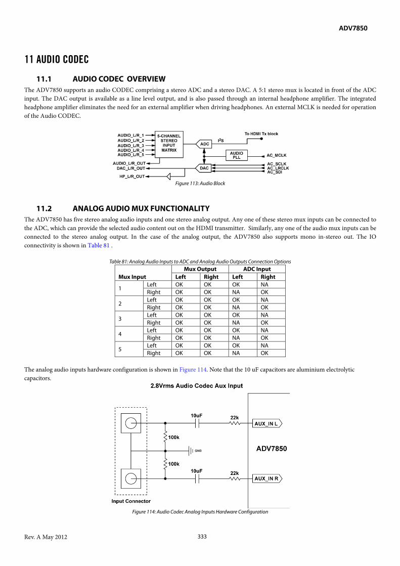
ADV7850
Rev. A May 2012 333
11 AUDIO CODEC
11.1 AUDIO CODEC OVERVIEW The ADV7850 supports an audio CODEC comprising a stereo ADC and a stereo DAC. A 5:1 stereo mux is located in front of the ADC input. The DAC output is available as a line level output, and is also passed through an internal headphone amplifier. The integrated headphone amplifier eliminates the need for an external amplifier when driving headphones. An external MCLK is needed for operation of the Audio CODEC.
Figure 113: Audio Block
11.2 ANALOG AUDIO MUX FUNCTIONALITY The ADV7850 has five stereo analog audio inputs and one stereo analog output. Any one of these stereo mux inputs can be connected to the ADC, which can provide the selected audio content out on the HDMI transmitter. Similarly, any one of the audio mux inputs can be connected to the stereo analog output. In the case of the analog output, the ADV7850 also supports mono in-stereo out. The IO connectivity is shown in Table 81 .
Table 81: Analog Audio Inputs to ADC and Analog Audio Outputs Connection Options
Mux Input Mux Output ADC Input
Left Right Left Right
1 Left OK OK OK NA Right OK OK NA OK
2 Left OK OK OK NA Right OK OK NA OK
3 Left OK OK OK NA Right OK OK NA OK
4 Left OK OK OK NA Right OK OK NA OK
5 Left OK OK OK NA Right OK OK NA OK
The analog audio inputs hardware configuration is shown in Figure 114. Note that the 10 uF capacitors are aluminium electrolytic capacitors.
Figure 114: Audio Codec Analog Inputs Hardware Configuration

ADV7850
Rev. A May 2012 334
11.2.1 Analog Audio ADC Input Selection The ADV7850 audio mux has five stereo pairs of analog audio inputs. adc_input_mux[2:0] selects which stereo pair of analog audio inputs will be available on the HDMI transmitter. The HDMI transmitter must be configured as required for this audio content (refer to Section 13). adc_input_mux[2:0], Addr 5C (audio_codec), Address 0x00[2:0] This control is used to set the ADC input mux options.
Function adc_input_mux[2:0] Description 000 No source 001 AUXIN1 010 AUXIN2 011 AUXIN3 100 AUXIN4 101 AUXIN5 Others Reserved
11.2.2 Analog Audio Mux Output Selection The ADV7850 audio mux has one stereo analog audio output. mux_out_l_sel[3:0] and mux_out_r_sel[3:0] select which analog audio inputs will be available on the stereo analog audio output. Using these controls, it is also possible to achieve mono in to stereo out functionality. The audio mux output is enabled using muxout_en. The ADV7850 audio codec provides a stereo output mux. The mux output hardware configuration is shown in Figure 115. Note that the 10 uF capacitors are aluminium electrolytic capacitors. The mux provides a 1 V rms output signal. If the mux output is used on a SCART output, an external line driver is required to restore the mux output signals to the SCART specification of 2.8 V rms.
Figure 115: Audio Codec Mux Output Hardware Configuration
muxout_en, Addr 5C (Audio Codec), Address 0x2C[0] This control is used to enable the audio mux output.

ADV7850
Rev. A May 2012 335
Function muxout_en Description 0 << Audio Mux Output not enabled 1 Enable Audio Mux Output
The audio content on the mux out left and right channels can be selected using mux_out_l_sel[3:0] and mux_out_r_sel[3:0]. mux_out_l_sel[3:0], Addr 5C (audio_codec), Address 0x0E[7:4] This control is used to select the analog input to mux to the analog output right channel.
Function mux_out_l_sel[3:0] Description 0000 No source 0001 AUXIN1_R 0010 AUXIN1_L 0011 AUXIN2_R 0100 AUXIN2_L 0101 AUXIN3_R 0110 AUXIN3_L 0111 AUXIN4_R 1000 AUXIN4_L 1001 AUXIN5_R 1010 AUXIN5_L Others Reserved
mux_out_r_sel[3:0], Addr 5C (audio_codec), Address 0x0E[3:0] This control is used to select the analog input to mux to the analog output left channel.
Function mux_out_r_sel[3:0] Description 0000 No source 0001 AUXIN1_R 0010 AUXIN1_L 0011 AUXIN2_R 0100 AUXIN2_L 0101 AUXIN3_R 0110 AUXIN3_L 0111 AUXIN4_R 1000 AUXIN4_L 1001 AUXIN5_R 1010 AUXIN5_L Others Reserved
11.2.3 Analog Audio Mux Input/Mux Output Configuration Overview The ADV7850 is designed to use a combination of internal and external resistances. Measured from the system audio input connector, the total nominal input impedance is 32.1 kΩ. All system audio inputs are designed to support 2.8 V rms audio input. Figure 116 shows a high level implementation overview.

ADV7850
Rev. A May 2012 336
Note: The analog audio input pins of the ADV7850 only see 880 mV RMS signals. However, the ADV7850 incorporates a gain stage to restore the mux output level to 1.0 V rms. An external line driver is required to restore the audio output signals to the SCART specification of 2.8 V rms.
Figure 116: High Level Overview of Analog Audio Mux Input/Mux Output Configuration
A factory calibration will be applied during final test to ensure that the gain through the mux circuit remains within +/-5%. Calibration is also applied to the ADC reference current to ensure the code swing from the ADC remains within +/-5% across the part for a given input. External impedances with a tolerance of +/-1% are required.
11.3 AUDIO CODEC FUNCTIONALITY The ADV7850 supports an audio CODEC comprising a stereo ADC and a stereo DAC. The DAC output is available as a line level output, and is also passed through an internal headphone amplifier. The output of the headphone amplifier can be used directly to drive stereo headphones. The audio CODEC requires an external MCLK. For an MCLK signal with a frequency of 3.072 MHz, 6.144 MHz, 12.288 MHz or 24.576 MHz, the ADC and DAC sample rates are 48 kHz. The user must ensure pll_ref_freq[1:0] is set correctly so that it always generates an internal MCLK of 6.144 MHz. A fixed oversample rate of 128X is implemented. If the MCLK is reduced to 2.8224 MHz, 5.6448 MHz, 11.2896 MHz or 22.5792 MHz the ADC and DAC sample rate will reduce to 44.1 kHz. The bandwidth of the digital filter is sufficient that a 20 kHz pass band is maintained in this mode. The word depth of both ADC and DAC is 24 bits. The ADC and DAC have independent LRCLK and SCLK signals, but use a common MCLK. The ADC supports I2S mode, providing LRCLK, SCLK and I2S signals. These signals are sent to the HDMI Tx and embedded into the HDMI stream. The DAC supports I2S mode. The LRCLK, SCLK and data signals must be provided by the back end SOC, and must be frequency locked with the MCLK but phase independent. The output level is 1 V rms full scale. There is one stereo headphone amplifier output capable of driving 32 Ω loads at 1 V rms. The headphone output incorporates circuitry to suppress pop/click sounds during the power on/off cycle.
11.3.1 Audio PLL The ADV7850 audio PLL generates the required internal analog and digital clocks for the audio CODEC. The PLL reference input signal is selected using pll_ref_freq[1:0]. The audio PLL requires external components to operate correctly, as shown in Figure 117. The placement and layout of these components should match the evaluation board layout. The 1000 pF capacitor is an NPO type capacitor.

ADV7850
Rev. A May 2012 337
Figure 117: Audio PLL Loop Filter Components
pll_ref_freq[1:0], Addr 5C (audio_codec), Address 0x00[7:6] This control is used to select the PLL reference input frequency.
Function pll_ref_freq[1:0] Description 00 512*Fs (24.576 MHz) 01 256*Fs (12.288 MHz) 10 128*Fs (6.144 MHz) 11 64*Fs (3.072 MHz)
audio_pll_locked indicates the lock status of the audio PLL. audio_pll_locked, Addr 5C (Audio Codec), Address 0x0D[0] (Read Only) This readback indicates the audio PLL locking status.
Function audio_pll_locked Description 0 << Unlocked 1 Locked
11.3.2 VREF_AUDIO, FILTA and FILTD (Location) The VREF_AUDIO, FILTA and FILTD pins require the external components shown in Figure 118 to ensure correct operation of the audio codec. The placement and layout of these components should match the evaluation board layout.

ADV7850
Rev. A May 2012 338
Figure 118: Audio Codec VREF AUDIO, FILTA and FILTD Configuration
11.3.3 DAC and Headphone Outputs The ADV7850 has an audio DAC output and a headphone output. The stereo DAC output is available as a line level output, and is also passed through an internal headphone amplifier. The integrated headphone amplifier eliminates the need for an external amplifier when driving headphones. The stereo headphone amplifier output is capable of driving 32 Ω loads at 1 V rms.
11.3.3.1 Audio Codec DAC Output The DAC analog audio output hardware configuration is shown in Figure 119. Note that the 10 uF capacitors are aluminium electrolytic capacitors. The 10,000 pF capacitors are ceramic NPO type capacitors.
Figure 119: Audio Codec DAC Output Hardware Configuration
11.3.3.2 Audio Codec Headphone Output The headphone output hardware configuration is shown in Figure 120. Note that the 100 uF capacitors are aluminium electrolytic

ADV7850
Rev. A May 2012 339
capacitors.
Figure 120: Audio Codec Headphone Output Hardware Configuration
To use the headphone output, the left and right headphone amplifiers must be powered up using hp_left_amp_pu and hp_right_amp_pu. The HPOUT_L and HPOUT_R pins are tristated by default. When the headphone output is in use, this tristate condition must be disabled using hp_left_tri_enb and hp_right_tri_enb. hp_left_tri_enb, Addr 5C (audio_codec), Address 0x05[1] This control is used to tristate the headphone left amplifier.
Function hp_left_tri_enb Description 0 Tristate headphone left amplifier 1 Do not tristate headphone left amplifier
hp_right_tri_enb, Addr 5C (audio_codec), Address 0x05[0] This control is used to tristate the headphone right amplifier.
Function hp_right_tri_enb Description 0 Tristate headphone right amplifier 1 Do not tristate headphone right amplifier
The headphone output can be muted using hp_mute. hp_mute, Addr 5C (audio_codec), Address 0x05[2] This control is used to mute the headphone amplifier.
Function hp_mute Description 0 Mute headphone amplifier 1 Unmute headphone amplifier
The headphone output level can be attenuated using hp1_atten[4:0].
ADV7850
Rev. A May 2012 340
hp1_atten[4:0], Addr 5C (audio_codec), Address 0x06[4:0] This control is used to set headphone amplifier attenuation (0 dB to -46.5 dB in -1.5 dB steps).
Function hp1_atten[4:0] Description 00000 0dB ...
hp_scp, Addr 5C (audio_codec), Address 0x05[3] This control is used to enable short circuit protection.
Function hp_scp Description 0 Enable short circuit protection 1 Disable short circuit protection
hp_clamp_op, Addr 5C (audio_codec), Address 0x07[1] This control is used to unclamp headphone outputs from AGND.
Function hp_clamp_op Description 0 Clamp output 1 Disable clamp
11.3.4 Volume Controls vol_dac_left[7:0], Addr 5C (audio_codec), Address 0x10[7:0] This control is used to set the volume control. Volume in dB = value * -0.375 dB vol_dac_right[7:0], Addr 5C (audio_codec), Address 0x11[7:0] This control is used to set the volume control. Volume in dB = value * -0.375 dB The DAC output is also available as a stereo headphone output. The headphone output level can be attenuated using the hp1_atten[4:0] control. vol_adc_left[7:0], Addr 5C (audio_codec), Address 0x18[7:0] This control is used to set the volume control. Volume in dB = value * -0.375 dB vol_adc_right[7:0], Addr 5C (audio_codec), Address 0x19[7:0] This control is used to set the volume control. Volume in dB = value * -0.375 dB

ADV7850
Rev. A May 2012 341
11.4 AUDIO POWER UP/DOWN CONTROLS The audio Codec includes power up and power down controls. eng_dig_pu, Addr 5C (audio_codec), Address 0x01[3] This control is used to power up the digital engine.
Function eng_dig_pu Description 0 Power down digital engine 1 Power up digital engine
pll_pu, Addr 5C (audio_codec), Address 0x01[2] This control is used to power up PLL.
Function pll_pu Description 0 Power down PLL 1 Power up PLL
ref_buf_pu, Addr 5C (audio_codec), Address 0x01[1] This control is used to power up the reference buffer.
Function ref_buf_pu Description 0 Power down reference buffer 1 Power up reference buffer
left_dac_1_pu, Addr 5C (audio_codec), Address 0x02[0] This control is used to power up the DAC left channel.
Function left_dac_1_pu Description 0 Power down DAC left channel 1 Power up DAC left channel
right_dac_1_pu, Addr 5C (audio_codec), Address 0x02[1] This control is used to power up the DAC right channel.
Function right_dac_1_pu Description 0 Power down DAC right channel 1 Power up DAC right channel
The stereo DAC output can be put into standby mode using dac_ana_stdby_dis. The individual left and right DAC outputs can also be put into standby mode using left_dac_1_ana_stdby and right_dac_1_ana_stdby. dac_ana_stdby_dis, Addr 5C (audio_codec), Address 0x01[0] This control is used to disable DAC analog standby.

ADV7850
Rev. A May 2012 342
Function dac_ana_stdby_dis Description 0 DACs in standby mode 1 DACs in normal mode
left_dac_1_ana_stdby, Addr 5C (audio_codec), Address 0x09[0] This control is used to set the DAC left channel into standby mode.
Function left_dac_1_ana_stdby Description 0 Full power 1 Set DAC left channel into standby mode
right_dac_1_ana_stdby, Addr 5C (audio_codec), Address 0x09[1] This control is used to set the DAC right channel into standby mode.
Function right_dac_1_ana_stdby Description 0 Full power 1 Set DAC right channel into standby mode
The DAC standby current can be set using dac_ana_stndby_adj[1:0]. dac_ana_stndby_adj[1:0], Addr 5C (audio_codec), Address 0x38[1:0] This control is used to adjust the DAC standby current.
Function dac_ana_stndby_adj[1:0]
Description
00 2 uA 01 4 uA 10 6 uA 11 12 uA
left_adc_1_pu, Addr 5C (audio_codec), Address 0x03[0] This control is used to power up the ADC left channel.
Function left_adc_1_pu Description 0 Power down ADC left channel 1 Power up ADC left channel
right_adc_1_pu, Addr 5C (audio_codec), Address 0x03[1] This control is used to power up the ADC right channel.

ADV7850
Rev. A May 2012 343
Function right_adc_1_pu Description 0 Power down ADC right channel 1 Power up ADC right channel
hp_left_amp_pu, Addr 5C (audio_codec), Address 0x05[4] This control is used to power up the headphone left amplifier.
Function hp_left_amp_pu Description 0 Power down headphone left amplifier 1 Power up headphone left amplifier
hp_right_amp_pu, Addr 5C (audio_codec), Address 0x05[5] This control is used to power up the headphone right amplifier.
Function hp_right_amp_pu Description 0 Power down headphone right amplifier 1 Power up headphone right amplifier
vref_enb, Addr 5C (audio_codec), Address 0x08[0] This control is used to disable the voltage reference.
Function vref_enb Description 0 Enable voltage reference 1 Disable voltage reference
ref_core_pd, Addr 5C (audio_codec), Address 0x33[6] This control is used to power down the reference core.
Function ref_core_pd Description 0 Power down reference core 1 Power up reference core
To place the Audio Codec into a powered down state, the I2C writes listed below should be used. If the audio codec is not being used, the below writes should also be carried out to ensure low power consumption. 5C 33 40 Power down reference 5C 08 01 Voltage reference disable 5C 01 11 Amplifier power down

ADV7850
Rev. A May 2012 344
12 MEMORY CONTROLLER
12.1 MEMORY REQUIREMENTS The ADV7850 supports a DDR2 memory interface. Depending on the feature required, the appropriate memory device can be selected. The external memory is required for 3D comb and Frame TBC operation only. The ADV7850 requires the following memory specifications:
• 128 Mb, 256 Mb, 512 Mb and 1Gb DDR2 SDRAM memory are supported • Memory architecture supports bus width of 16 bits • Minimum speed grade of 108 MHz and an integer CAS latency is required • Example of 512 Mb compatible memory includes Micron MT47H32M16HR-25EG • 47 Ω series termination resistors are recommended for this configuration
12.2 GENERAL CONTROLS
12.2.1 Reset
A reset should be carried out after changes to the memory configuration. The reset is required before the configuration settings are implemented in the ADV7850. sdp_mem_reset, IO, Address 0xFF[2] (Self-Clearing) Memory interface reset.
Function sdp_mem_reset Description 0 << Not reset 1 Apply SDP Memory reset
12.2.2 Output Enables ddr2_ck_oe, XMEM_GAMMA, Address 0x28[6] This control is used to enable the external memory clock signal.
Function ddr2_ck_oe Description 0 Input 1 Output
rw_ctrl_oe, XMEM_GAMMA, Address 0x28[7] This control is used to enable the external memory read/write signals, e.g. ras, cas, clock, and address.

ADV7850
Rev. A May 2012 345
Function rw_ctrl_oe Description 0 Input 1 Output
12.3 DRIVE STRENGTH CONTROLS The drive strength of signals from the ADV7850 memory interface can be configured with the following controls. The clock and the DQS outputs have independent drive strength controls. dqs_drv_str[7:0], XMEM_GAMMA, Address 0x39[7:0] This control is used to adjust the drive strength setting for the upper DQS outputs to the DDR2 memory.
Function dqs_drv_str[7:0] Description 00 Minimum drive strength FF Maximum drive strength
ck_drv_str[7:0], XMEM_GAMMA, Address 0x37[7:0] This control is used to adjust the drive strength setting for the clock output to the DDR2 memory.
Function ck_drv_str[7:0] Description 00 Minimum drive strength FF Maximum drive strength
mem_rw_ctrl_drv_str[1:0], XMEM_GAMMA, Address 0x28[1:0] This control is used to adjust the drive strength setting for the read/write control signals to the DDR2 memory, e.g. ras, cas, wr, and cke.
Function mem_rw_ctrl_drv_str[1:0]
Description
00 Minimum drive strength 11 Maximum drive strength
12.4 DDR2 BIST TEST The ADV7850 features a DDR2 Built-In Self Test (BIST) block to allow testing of the ADV7850 DDR2 interface. The BIST allows the ADV7850 and the external memory to be tested in circuit. The test is fully self-contained and does not require any external stimulus. When the BIST test block is enabled, it controls the commands sent to the DDR2 controller of the ADV7850 and generates pseudo random data and addresses using a defined protocol. The controller first writes a number of random 32-bit words to the external memory. The same number of reads are then performed from the written addresses. The readback is compared with the pseudo random data generated to check if there are any errors. The controller will continue to output and read back pseudo random data until the ADV7850 is reset. Once a fail is detected, SDRAM_BIST_ERROR is set high. This bit can only be cleared by a system reset. The results are available via I2C readback.

ADV7850
Rev. A May 2012 346
Figure 121: DDR2 BIST Test Architecture
A DDR2 BIST test is initialized and started via the following writes: 40 F1 90 SDP map address 40 F2 94 SDPIO map address 40 EB A8 Memory map address 40 0C 40 Power up core 40 15 80 Power up pads A0 00 00 CVBS 2x1 mode A0 01 00 SD mode A8 11 32 ADI recommended write A8 2B 08 ADI recommended write A8 08 D2 ADI recommended write (memory initialization) A8 07 20 ADI recommended write (memory initialization) A8 06 20 ADI recommended write (memory initialization) A8 05 01 ADI recommended write (memory initialization) A8 28 E5 Output enable for SDRAM clock pad and other output pads A8 27 07 Memory reference enabled A8 26 12 ADI recommended write (memory initialization) A8 23 10 ADI recommended write A8 24 10 ADI recommended write A8 25 05 ADI recommended write 40 C8 84 ADI recommended write 40 CA 84 ADI recommended write 90 D4 40 ADI recommended write A8 1e 43 ADI recommended write A8 1f 02 ADI recommended write A8 20 80 ADI recommended write A8 21 C1 ADI recommended write 94 80 80 ADI recommended write (BIST initialization) 94 81 03 ADI recommended write (BIST initialization) 94 82 8E ADI recommended write (BIST initialization) 94 83 00 ADI recommended write (BIST initialization) 94 84 07 ADI recommended write (BIST initialization) 94 85 1C ADI recommended write (BIST initialization) 90 12 01 3D comb enabled 94 7C 18 ADI recommended write (BIST initialization) 40 FF 0C Memory reset A8 2B 0A ADI recommended write (BIST start)
LoopbackTest Logic
DDR2Controller
Phy 512M x 16 External DDR2 Memory
32-bit Data
Address
Control
Address
Control
16-bit Data32-bit Data

ADV7850
Rev. A May 2012 347
The result of the DDR2 loopback test is given by SDRAM_BIST_DONE and SDRAM_BIST_ERROR. sdram_bist_done, Addr 94 (sdp_IO), Address 0xDB[4] (Read Only)
Function sdram_bist_done Description 1 Memory controller BIST has begun checking data integrity 0 << Memory controller BIST has not begun checking data integrity
sdram_bist_error, Addr 94 (sdp_IO), Address 0xDB[5] (Read Only)
Function sdram_bist_error Description 1 Memory controller BIST has detected an error. It is only valid if SDRAM_BIST_DONE is set. 0 << Memory controller BIST has not detected an error.
The following possible failures can cause the DDR2 BIST test to fail:
• Address or control or clock open or short circuit • Single DQ open or short to ground or supply, a single bit line failing on both positive and negative edges • Short between DQ lines, 2-bit lines failing, routing in adjacent resistors of resistor pack • DQS or DM open or short, up to eight DQ lines failing • Timing transfer problem, one or more bit lines failing
12.5 EXTERNAL MEMORY LAYOUT GUIDELINES The ADV7850 should be placed as close to and on the same side as the external DDR2 memories. Balanced T-routing should be used for all shared connections between the ADV7850 and the external DDR2 memories. All traces should be 75 ohm and impedance controlled to ensure robust timing. Traces should be routed on the same layer as the devices, where possible. If this is not possible, all traces should be kept on the outer layers. All differential signals (for example, DDR_CK and DDR_CKB) should be treated as described here. These signals should be routed in parallel and on the same side of the PCB. The DDR_CK trace length should be matched to the DDR_CKB trace length to 20 mils (0.5 mm). Any stubs on the clock lines should be kept as short as possible to avoid signal reflections. The following 4-byte wide data lanes should be matched to within 50 mils on the PCB layout. The precise matching of these signals is critical.
• DDR3_DM3, DDR_DQS3, DDR_DQSB3, DDR_DQ31 to DDR_DQ24 • DDR2_DM2, DDR_DQS2, DDR_DQSB2, DDR_DQ23 to DDR_DQ16 • DDR1_DM1, DDR_DQS1, DDR_DQSB1, DDR_DQ15 to DDR_DQ8 • DDR0_DM0, DDR_DQS0, DDR_DQSB0, DDR_DQ7 to DDR_DQ0
Different byte lanes are to be matched to 200 mils (5.08 mm) of each other. 47-Ohm series termination resistors should be placed as close to the source (ADV7850) as possible on the following signals:
• Address signals – DDR_A12 to DDR_A0 and DDR_BA0 to DDR_BA2 • Clock differential signals – DDR_CK and DDR_CKB (discrete resistors are used for these two signals) • Control signal – DDR_CKE, and command signals – DDR_CSB, DDR_RASB, DDR_CASB, and DDR_WEB • Data mask signals – DDR_DM3 to DDR_DM0
47-Ohm series termination resistors should be placed in the middle of the trace on the following signals:

ADV7850
Rev. A May 2012 348
• Data bus signals – DDR_DQ31 to DDR_DQ0 • Data strobe signals – DDR_DQS3_DDR_DQS3B to DDR_DQS0 DDR_DQS0B
The DDR2 reference voltage (DDR_VREF) should be routed as far away as possible from other the signals to avoid any variations in the voltage. This trace should be wide. There should be a 100 nF decoupling cap close to the DDR2 reference voltage pins as well as the ADV7850 reference pin.

ADV7850
Rev. A May 2012 349
13 HDMI TRANSMITTER
Figure 122: Functional Block Diagram of HDMI Tx Core
13.1 GENERAL OPERATION The HDMI Transmitter on the ADV7850 can provides support for up to 3GHz. The Transmitter is designed to pass full HDMI compliance up to 225MHz and can operate up to 3GHz when directly connected to a backend system in a closed configuration. The ADV7850 Transmitter can be configured in a mux mode and non-mux mode. These modes are described in the HDMI Rx section of this manual. For the HDMI Transmitter in mux mode, InfoFrame editing is not supported and audio insertion is also not supported.
13.2 GENERAL CONTROLS To operate the HDMI Tx core, it is necessary to monitor the Hot Plug Detect (HPD) signal from the downstream sink and power up the Tx core after the appropriate HPD becomes high. To power up the Tx core, system_pd must be programmed to 0 when the TX_HPD pin is high. The status of the TX_HPD pin is provided via the hpd_state. Some registers cannot be written to when the signal on the TX_HPD input pin is low. Some registers will be reset to their default value when the level on the TX_HPD pin goes from high to low. The best method to determine when the level of the signal on the TX_HPD pin is high is to use the interrupt system. An interrupt can be enabled to notify level change on the TX_HPD pin (refer to Section 15 for more information regarding the ADV7850 interrupts). The ADV7850 also features a status bit, rx_sense, which can be used to detect the presence of TMDS clock terminations from the sink. If the ADV7850 detects a voltage level higher than 1.8 V on the clock lines of its TMDS output port, rx_sense_interrupt is triggered and rx_sense is set to 1. The detection of TMDS clock terminations from downstream sink devices is useful to delay powering up the transmitter sections until the downstream sink devices are actually ready to receive signals. A typical implementation for a sink is to tie the transmitter 5 V power signal to HPD through a series resistor. In this case, the ADV7850 will detect a high level on TX_HPD regardless of whether or not the downstream sink is powered on and ready to receive a TMDS stream. For this reason, it is best to wait for both rx_sense and hpd_state to be high before powering up the Tx core when trying to achieve minimum power consumption. system_pd, Addr B8 (Main), Address 0x41[6] This control is used to power down the HDMI Tx.
TXPacket Builder
TX_0
TxAudio Receiver
TxHDCP
Encryption
TxHDCPKeys
TxHDMI Encode TX_1
TX_2
TX_C
AUD_IN [5:0]
MCLKIN
Data [35:0]
HS
VS
DE
Video_data [23:0]
HS
VS
DE
Tx Video Path
TxTMDS PLL
Serializer andDrivers
clk_out
clk_d ata
Audio_data [8:0]
Video_data[23:0]
Audio_data
Video_data[23:0]
Audio_data [8:0]
Ch0 [9:0]
Ch1 [9:0]
Ch2 [9:0]
DEEP COLOR CONV
Simplified444 -> 422
Format Detect
Black level
enable
Pixel repitition
HS
VS
VIC code
I2C
PLL m
PLL n
AVI _vid
[8:0]
SCLK

ADV7850
Rev. A May 2012 350
Function system_pd Description 0 Normal operation 1 Power down ADV7850 Tx
hpd_state, Addr B8 (Main), Address 0x42[6] (Read Only) This readback displays the state of the hot plug detection.
Function hpd_state Description 0 Low hot plug detect state 1 High hot plug detect state
rx_sense, Addr B8 (Main), Address 0xC6[2] (Read Only) This readback indicates whether or not the receiver detected a TMDS pullup on the clock signal line.
Function rx_sense Description 0 TMDS clock pullup not present 1 TMDS clock pullup present
tx_hpd_override, IO, Address 0x2C[0] This control is used to allow the HDMI Tx to power on when HPD is low.
Function tx_hpd_override Description 0 Normal operation 1 HPD override
13.3 HDMI DVI SELECTION The HDMI Tx core supports the transmission of both HDMI and DVI streams. The type of stream the ADV7850 transmits is set via hdmi_mode_sel. In DVI transmission mode, no packets will be sent and all registers relating to packets and InfoFrames will be disregarded. The current transmission mode can be confirmed by reading hdmi_mode. hdmi_mode_sel, Addr B8 (Main), Address 0xAF[2] This control is used to set the HDMI mode. In automatic mode, audio detection will put the Tx into HDMI mode.
Function hdmi_mode_sel Description 0 Set automatic mode 1 Set DVI/HDMI mode
hdmi_mode, Addr 72 (Main), Address 0xC6[4] (Read Only) HDMI mode status.

ADV7850
Rev. A May 2012 351
Function HDMI_MODE Description 0 << DVI 1 HDMI
13.4 AV MUTE The AV mute status is sent to the downstream sink through the general control packet. One purpose of the AV mute is to alert the sink of a change in the TMDS clock so the sink can mute audio and video while the TMDS clock it receives is unstable. Setting AV mute also pauses HDCP encryption, so the HDCP link between the HDMI Tx and the sink is maintained while the TMDS clock is not stable. Note that AV mute is not sufficient as a means to hide protected content because the content is still sent even when AV mute is enabled. To use AV mute:
• Enable the GCP by setting gcp_pkt_en to 1 • To set AV mute, clear clear_avmute and set set_avmute • To clear AV mute, clear set_avmute and set clear_avmute
Note that setting both set_avmute and clear_avmute is not a valid configuration. set_avmute, Addr B8 (Main), Address 0x4B[6] This control is used to set the set AV mute signal.
Function set_avmute Description 0 Clear the set AV mute signal 1 Set the set AV mute signal
clear_avmute, Addr B8 (Main), Address 0x4B[7] This control is used to set the clear AV mute signal.
Function clear_avmute Description 0 Clear the clear AV mute signal 1 Set clear AV mute signal
13.5 TX SQUELCH FEATURE The ADV7850 provides a squelch feature to mute the video clock when there is no input connected to the HDMI Input. This feature ensures that no spurious clocks signals are output to the backend device when a cable is disconnected or an input source switches off. The feature can mute the video based on TMDS detection in the HDMI Receiver and/or on the incoming HSync signal to the HDMI Receiver. This feature should be disabled for Analog input modes. The following table highlights the available options.
Table 82 : TX Squelch Configuration Options
HSync Activity Detect
TMDS Clock Detect Functionality
0 0 Use TMDS Clock detect to power down HDMI Tx clock and data lines 1 0 Use HSync Activity Detect and TMDS Clock detect to power down HDMI Tx clock and
data lines 0 1 Disable the feature ( Recommend setting for analog input modes) 1 1 Reserved – Not Used

ADV7850
Rev. A May 2012 352
video_clock_detect, Addr B8 (Main), Address 0xEF[2] This control is used to enable the HDMI Tx Squelch feature. This should be set to 0 in all analog input modes.
Function video_clock_detect Description 1 Disable TMDS Clock detection (and HSync activity Detect) 0 Enable TMDS clock detection (and HSync Activity Detect if enabled)
hs_active_det_en, Addr B8 (Main), Address 0xFE[1] This control is used to enable HSync activity detection for the HDMI Tx Squelch feature. This should be set to 0 in all analog input modes.
Function hs_active_det_en Description 0 Disable HSync Activity Detect 1 Enable HSync activity Detect
13.6 SOURCE PRODUCT DESCRIPTION INFOFRAME The Source Product Description (SPD) InfoFrame contains the vendor name and product description. The transmission of SPD InfoFrames is enabled by setting spd_pkt_en to 1. When it is set, the HDMI Tx section transmits one SPD packet once every two video fields. An application of this packet is to allow the sink to display the source information using an OSD. This information is in a 7-bit ASCII format. Refer to the CEA 861 specification for more details. spd_pkt_en, Addr B8 (Main), Address 0x40[6] This control is used to enable an SPD packet.
Function spd_pkt_en Description 0 Disable SPD packet 1 Enable SPD packet
Table 83: SPD InfoFrame Configuration Register
Tx Packet Memory Map Address
Access Type Register Name Default Value Byte Name
0x00 R/W spd_hb0[7:0] 0x00 SPD Header Byte 0 0x01 R/W spd_hb1[7:0] 0x00 SPD Header Byte 1 0x02 R/W spd_hb2[7:0] 0x00 SPD Header Byte 2 0x03 R/W spd_pb0[7:0] 0x00 SPD Data Byte 0 0x04 R/W spd_pb1[7:0] 0x00 SPD Data Byte 1 0x05 R/W spd_pb2[7:0] 0x00 SPD Data Byte 2 0x06 R/W spd_pb3[7:0] 0x00 SPD Data Byte 3 0x07 R/W spd_pb4[7:0] 0x00 SPD Data Byte 4 0x08 R/W spd_pb5[7:0] 0x00 SPD Data Byte 5 0x09 R/W spd_pb6[7:0] 0x00 SPD Data Byte 6 0x0A R/W spd_pb7[7:0] 0x00 SPD Data Byte 7 0x0B R/W spd_pb8[7:0] 0x00 SPD Data Byte 8 0x0C R/W spd_pb9[7:0] 0x00 SPD Data Byte 9 0x0D R/W spd_pb10[7:0] 0x00 SPD Data Byte 10 0x0E R/W spd_pb11[7:0] 0x00 SPD Data Byte 11 0x0F R/W spd_pb12[7:0] 0x00 SPD Data Byte 12 0x10 R/W spd_pb13[7:0] 0x00 SPD Data Byte 13

ADV7850
Rev. A May 2012 353
Tx Packet Memory Map Address
Access Type Register Name Default Value Byte Name
0x11 R/W spd_pb14[7:0] 0x00 SPD Data Byte 14 0x12 R/W spd_pb15[7:0] 0x00 SPD Data Byte 15 0x13 R/W spd_pb16[7:0] 0x00 SPD Data Byte 16 0x14 R/W spd_pb17[7:0] 0x00 SPD Data Byte 17 0x15 R/W spd_pb18[7:0] 0x00 SPD Data Byte 18 0x16 R/W spd_pb19[7:0] 0x00 SPD Data Byte 19 0x17 R/W spd_pb20[7:0] 0x00 SPD Data Byte 20 0x18 R/W spd_pb21[7:0] 0x00 SPD Data Byte 21 0x19 R/W spd_pb22[7:0] 0x00 SPD Data Byte 22 0x1A R/W spd_pb23[7:0] 0x00 SPD Data Byte 23 0x1B R/W spd_pb24[7:0] 0x00 SPD Data Byte 24 0x1C R/W spd_pb25[7:0] 0x00 SPD Data Byte 25 0x1D R/W spd_pb26[7:0] 0x00 SPD Data Byte 26 0x1E R/W spd_pb27[7:0] 0x00 SPD Data Byte 27
13.7 SPARE PACKETS The user can configure the ADV7850 to send any type of packets or InfoFrames via the spare packets controls and associated configuration registers. The ADV7850 features two such spare packets that can be enabled via the spare_pkt0_en and spare_pkt1_en controls. When a spare packet is enabled, the Tx transmits one of these enabled spare packets once every two video fields. spare_pkt0_en, Addr B8 (Main), Address 0x40[0] This control is used to enable spare_packet0.
Function spare_pkt0_en Description 0 Disable spare_packet0 1 Enable spare_packet0
spare_pkt1_en, Addr B8 (Main), Address 0x40[1] This control is used to enable spare_packet1.
Function spare_pkt1_en Description 0 Disable spare_packet1 1 Enable spare_packet1
Table 84: Spare Packet 1 Configuration Register
Tx Packet Memory Map Address
Access Type Register Name Default Value Byte Name
0xC0 R/W spare1_hb0[7:0] 0x00 Spare Packet Header Byte 0 0xC1 R/W spare1_hb1[7:0] 0x00 Spare Packet Header Byte 1 0xC2 R/W spare1_hb2[7:0] 0x00 Spare Packet Header Byte 2 0xC3 R/W spare1_pb0[7:0] 0x00 Spare Packet Data Byte 0 0xC4 R/W spare1_pb1[7:0] 0x00 Spare Packet Data Byte 1 0xC5 R/W spare1_pb2[7:0] 0x00 Spare Packet Data Byte 2 0xC6 R/W spare1_pb3[7:0] 0x00 Spare Packet Data Byte 3 0xC7 R/W spare1_pb4[7:0] 0x00 Spare Packet Data Byte 4 0xC8 R/W spare1_pb5[7:0] 0x00 Spare Packet Data Byte 5 0xC9 R/W spare1_pb6[7:0] 0x00 Spare Packet Data Byte 6 0xCA R/W spare1_pb7[7:0] 0x00 Spare Packet Data Byte 7 0xCB R/W spare1_pb8[7:0] 0x00 Spare Packet Data Byte 8 0xCC R/W spare1_pb9[7:0] 0x00 Spare Packet Data Byte 9 0xCD R/W spare1_pb10[7:0] 0x00 Spare Packet Data Byte 10

ADV7850
Rev. A May 2012 354
Tx Packet Memory Map Address
Access Type Register Name Default Value Byte Name
0xCE R/W spare1_pb11[7:0] 0x00 Spare Packet Data Byte 11 0xCF R/W spare1_pb12[7:0] 0x00 Spare Packet Data Byte 12 0xD0 R/W spare1_pb13[7:0] 0x00 Spare Packet Data Byte 13 0xD1 R/W spare1_pb14[7:0] 0x00 Spare Packet Data Byte 14 0xD2 R/W spare1_pb15[7:0] 0x00 Spare Packet Data Byte 15 0xD3 R/W spare1_pb16[7:0] 0x00 Spare Packet Data Byte 16 0xD4 R/W spare1_pb17[7:0] 0x00 Spare Packet Data Byte 17 0xD5 R/W spare1_pb18[7:0] 0x00 Spare Packet Data Byte 18 0xD6 R/W spare1_pb19[7:0] 0x00 Spare Packet Data Byte 19 0xD7 R/W spare1_pb20[7:0] 0x00 Spare Packet Data Byte 20 0xD8 R/W spare1_pb21[7:0] 0x00 Spare Packet Data Byte 21 0xD9 R/W spare1_pb22[7:0] 0x00 Spare Packet Data Byte 22 0xDA R/W spare1_pb23[7:0] 0x00 Spare Packet Data Byte 23 0xDB R/W spare1_pb24[7:0] 0x00 Spare Packet Data Byte 24 0xDC R/W spare1_pb25[7:0] 0x00 Spare Packet Data Byte 25 0xDD R/W spare1_pb26[7:0] 0x00 Spare Packet Data Byte 26 0xDE R/W spare1_pb27[7:0] 0x00 Spare Packet Data Byte 27
Table 85: Spare Packet 2 Configuration Register
Tx Packet Memory Map Address
Access Type Register Name Default Value Byte Name
0xE0 R/W spare2_hb0[7:0] 0x00 Spare Packet Header Byte 0 0xE1 R/W spare2_hb1[7:0] 0x00 Spare Packet Header Byte 1 0xE2 R/W spare2_hb2[7:0] 0x00 Spare Packet Header Byte 2 0xE3 R/W spare2_pb0[7:0] 0x00 Spare Packet Data Byte 0 0xE4 R/W spare2_pb1[7:0] 0x00 Spare Packet Data Byte 1 0xE5 R/W spare2_pb2[7:0] 0x00 Spare Packet Data Byte 2 0xE6 R/W spare2_pb3[7:0] 0x00 Spare Packet Data Byte 3 0xE7 R/W spare2_pb4[7:0] 0x00 Spare Packet Data Byte 4 0xE8 R/W spare2_pb5[7:0] 0x00 Spare Packet Data Byte 5 0xE9 R/W spare2_pb6[7:0] 0x00 Spare Packet Data Byte 6 0xEA R/W spare2_pb7[7:0] 0x00 Spare Packet Data Byte 7 0xEB R/W spare2_pb8[7:0] 0x00 Spare Packet Data Byte 8 0xEC R/W spare2_pb9[7:0] 0x00 Spare Packet Data Byte 9 0xED R/W spare2_pb10[7:0] 0x00 Spare Packet Data Byte 10 0xEE R/W spare2_pb11[7:0] 0x00 Spare Packet Data Byte 11 0xFF R/W spare2_pb12[7:0] 0x00 Spare Packet Data Byte 12 0xF0 R/W spare2_pb13[7:0] 0x00 Spare Packet Data Byte 13 0xF1 R/W spare2_pb14[7:0] 0x00 Spare Packet Data Byte 14 0xF2 R/W spare2_pb15[7:0] 0x00 Spare Packet Data Byte 15 0xF3 R/W spare2_pb16[7:0] 0x00 Spare Packet Data Byte 16 0xF4 R/W spare2_pb17[7:0] 0x00 Spare Packet Data Byte 17 0xF5 R/W spare2_pb18[7:0] 0x00 Spare Packet Data Byte 18 0xF6 R/W spare2_pb19[7:0] 0x00 Spare Packet Data Byte 19 0xF7 R/W spare2_pb20[7:0] 0x00 Spare Packet Data Byte 20 0xF8 R/W spare2_pb21[7:0] 0x00 Spare Packet Data Byte 21 0xF9 R/W spare2_pb22[7:0] 0x00 Spare Packet Data Byte 22 0xFA R/W spare2_pb23[7:0] 0x00 Spare Packet Data Byte 23 0xFB R/W spare2_pb24[7:0] 0x00 Spare Packet Data Byte 24 0xFC R/W spare2_pb25[7:0] 0x00 Spare Packet Data Byte 25 0xFD R/W spare2_pb26[7:0] 0x00 Spare Packet Data Byte 26 0xFE R/W spare2_pb27[7:0] 0x00 Spare Packet Data Byte 27
13.8 SYSTEM MONITORING
13.8.1 General Status and Interrupts
The ADV7850 utilizes both interrupts and status bits to indicate the status of internal operations and errors in the Tx core. These interrupt and status are listed in Table 86, Table 87, and Table 88.
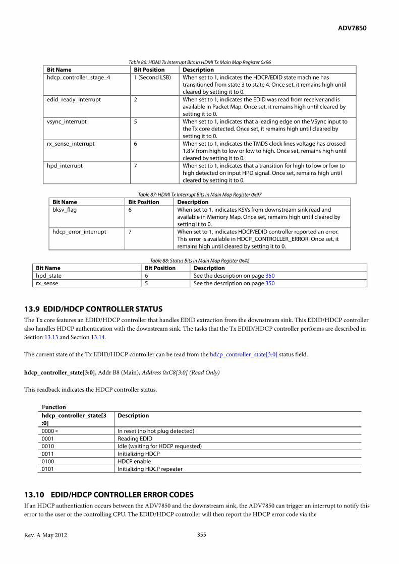
ADV7850
Rev. A May 2012 355
Table 86: HDMI Tx Interrupt Bits in HDMI Tx Main Map Register 0x96
Bit Name Bit Position Description hdcp_controller_stage_4 1 (Second LSB) When set to 1, indicates the HDCP/EDID state machine has
transitioned from state 3 to state 4. Once set, it remains high until cleared by setting it to 0.
edid_ready_interrupt 2 When set to 1, indicates the EDID was read from receiver and is available in Packet Map. Once set, it remains high until cleared by setting it to 0.
vsync_interrupt 5 When set to 1, indicates that a leading edge on the VSync input to the Tx core detected. Once set, it remains high until cleared by setting it to 0.
rx_sense_interrupt 6 When set to 1, indicates the TMDS clock lines voltage has crossed 1.8 V from high to low or low to high. Once set, remains high until cleared by setting it to 0.
hpd_interrupt 7 When set to 1, indicates that a transition for high to low or low to high detected on input HPD signal. Once set, remains high until cleared by setting it to 0.
Table 87: HDMI Tx Interrupt Bits in Main Map Register 0x97
Bit Name Bit Position Description bksv_flag 6 When set to 1, indicates KSVs from downstream sink read and
available in Memory Map. Once set, remains high until cleared by setting it to 0.
hdcp_error_interrupt 7 When set to 1, indicates HDCP/EDID controller reported an error. This error is available in HDCP_CONTROLLER_ERROR. Once set, it remains high until cleared by setting it to 0.
Table 88: Status Bits in Main Map Register 0x42
Bit Name Bit Position Description hpd_state 6 See the description on page 350 rx_sense 5 See the description on page 350
13.9 EDID/HDCP CONTROLLER STATUS The Tx core features an EDID/HDCP controller that handles EDID extraction from the downstream sink. This EDID/HDCP controller also handles HDCP authentication with the downstream sink. The tasks that the Tx EDID/HDCP controller performs are described in Section 13.13 and Section 13.14. The current state of the Tx EDID/HDCP controller can be read from the hdcp_controller_state[3:0] status field. hdcp_controller_state[3:0], Addr B8 (Main), Address 0xC8[3:0] (Read Only) This readback indicates the HDCP controller status.
Function hdcp_controller_state[3:0]
Description
0000 In reset (no hot plug detected) 0001 Reading EDID 0010 Idle (waiting for HDCP requested) 0011 Initializing HDCP 0100 HDCP enable 0101 Initializing HDCP repeater
13.10 EDID/HDCP CONTROLLER ERROR CODES If an HDCP authentication occurs between the ADV7850 and the downstream sink, the ADV7850 can trigger an interrupt to notify this error to the user or the controlling CPU. The EDID/HDCP controller will then report the HDCP error code via the

ADV7850
Rev. A May 2012 356
hdcp_controller_error[3:0] status field. The error code is only valid when hdcp_error_interrupt is set to 1. The last error code will remain in the HDCP/EDID controller error field even when the interrupt is cleared. hdcp_controller_error[3:0], Addr B8 (Main), Address 0xC8[7:4] (Read Only) This readback indicates the HDCP error information.
Function hdcp_controller_error[3:0]
Description
0000 No error 0001 Bad receiver Bksv 0010 Ri mismatch 0011 Pj mismatch 0100 I2C error (usually a no-ack) 0101 Time out waiting for downstream repeater 0110 Maximum cascade of repeaters exceeded 0111 SHA-1 hash check of KSV list failed 1000 Too many devices connected to repeater tree
13.11 VIDEO SETUP
13.11.1 Input Format
The HDMI Tx core of the ADV7850 receives video data from the ADV7850 digital core via a 36-bit wide bus and four synchronization signals; the pixel clock, the data enable, the horizontal and the vertical synchronization signals. The HDMI Tx core always receives the video data in a 4:4:4 and SDR format.
Figure 123: Format of Video Data Input into HDMI Tx Core
13.11.2 Video Mode Detection
The video mode detection feature can inform the user of the CEA 861 defined Video Identification Code (VIC) of the video being input to the Tx core, as well as some additional formats. If a CEA 861 format is detected, the VIC is contained in vfe_fmt_vid[5:0]. Some additional non CEA 861 formats are contained in vfe_aux_vid[2:0]. For some standards for which the VIC cannot be detected, the user needs to configure the following registers:
• The aspect ratio (set via asp_ratio) is used to distinguish between CEA 861 video timing codes where the aspect ratio is the only difference.
• For 240p and 288p modes, the number of total lines can be selected in vfe_prog_mode[1:0]. • The VIC detected is also affected by the pixel repetition.
The detected VIC is sent in the AVI InfoFrames unless pixel repetition is applied to the video stream transmitted by the ADV7850. When pixel repetition is applied to the video data, the VIC sent in the AVI InfoFrame may be different as the VIC is automatically determined by the ADV7850. To override the VIC detection, the pixel repetition mode must be set to manual by setting pr_mode[1:0] to 0b10 or 0b11. The desired VIC is then set. The Tx core can support non CEA 861 formats but the VIC will not be automatically detected for these
B/Cb0
B/Cb1
B/Cb2
B/Cb3
B/Cb4
...
R/Cr0
R/Cr1
R/Cr2
R/Cr3
R/Cr4
...
Bit 12-0
Bit 12-0
ComponentChannel
Pixel0 Pixel1 Pixel2 Pixel3 Pixel4 ...
Cb
Cr
Y G/Y0
G/Y1
G/Y2
G/Y3
G/Y4
...Bit 12-0

ADV7850
Rev. A May 2012 357
formats. In this case, the VIC should be manually set to 0. vfe_fmt_vid[5:0], Addr B8 (Main), Address 0x3E[7:2] (Read Only) This readback indicates the VIC detected by the video front end. vfe_aux_vid[2:0], Addr B8 (Main), Address 0x3F[7:5] (Read Only) This readback indicates the video input formats that are not inside the 861B table.
Function vfe_aux_vid[2:0] Description 000 Set by vfe_fmt_vid 001 240p not active 010 576i not active 011 288p not active 100 480i active 101 240p active 110 576i active 111 288p active
asp_ratio, Addr B8 (Main), Address 0x17[1] This control is used to set the aspect ratio of the input video.
Function asp_ratio Description 0 4:3 1 16:9
vfe_prog_mode[1:0], Addr B8 (Main), Address 0x3F[4:3] (Read Only) This readback indicates the progressive mode information about 240p and 288p.
Function vfe_prog_mode[1:0] Description 01 262 lines (240p),312 lines (288p) 10 263 lines(240p),313 lines (288p) 11 undefined(240p),314lines (288p)
13.11.3 Pixel Repetition
Pixel repetition is used in HDMI to increase the amount of blanking period available to send packets or to increase the pixel clock to meet the minimum TMDS clock rate of 25 MHz. The ADV7850 offers three choices for the user to implement pixel repetition in the Tx core. These choices or modes are described below and can be set via pr_mode[1:0]. Automatic mode: In automatic mode, the ADV7850 uses the audio sampling rate and the detected VIC information as parameters to decide if pixel repetition is needed to obtain sufficient blanking periods to send the audio. For an I2S input stream, the sampling rate is always set by the user via i2s_sf[3:0]. If the pixel repetition factor is adjusted to meet bandwidth requirements, the detected input VIC may be different from the VIC sent to the downstream sink. The VIC of the actual video sent across the HDMI link to the downstream sink, and which is included in the AVI InfoFrame, can be read from vid_to_rx[5:0]. Manual mode: In manual pixel repetition mode, the VIC sent in the AVI InfoFrame needs to be set. The factor between the pixel clock input to the Tx core and the output TMDS clock frequency must be programmed in ext_pll_pr[1:0]. The pixel repetition value sent to the HDMI sink

ADV7850
Rev. A May 2012 358
must be programmed in ext_target_pr[1:0]. Refer to the latest HDMI specification for more details on valid pixel repetition formats. Max mode: Max mode works in the same way as automatic mode, except that it always selects the highest pixel repetition factor the Tx core is capable of. This makes the video timing independent of the audio sampling rate. This mode is not typically used. pr_mode[1:0], Addr B8 (Main), Address 0x3B[6:5] This control is used to select the pixel repetition mode.
Function pr_mode[1:0] Description 00 Auto mode 01 Maximum mode 10 Manual mode 11 Manual mode
ext_pll_pr[1:0], Addr B8 (Main), Address 0x3B[4:3] This control is used to set the value for PLL pixel repetition.
Function ext_pll_pr[1:0] Description 00 x1 01 x2 10 x4 11 x4
ext_target_pr[1:0], Addr B8 (Main), Address 0x3B[2:1] This control is used to set the pixel repetition number to send to the Rx.
Function ext_target_pr[1:0] Description 00 x1 01 x2 10 x4 11 x4
vid_to_rx[5:0], Addr B8 (Main), Address 0x3D[5:0] (Read Only) This readback indicates the actual VIC sent to the HDMI Rx.
13.11.4 Video Related Packets and InfoFrames
Video related packets and InfoFrames, which include the AVI InfoFrame, MPEG InfoFrame and Gamut Metadata packet (GMP), are described in Section 13.11.5, Section 13.11.6, and Section 13.11.7.
13.11.5 AVI InfoFrame
The AVI InfoFrame is defined in the latest CEA 861 specification. The user can enable the transmission of AVI InfoFrames to the downstream sink by setting aviif_pkt_en. When the transmission of AVI InfoFrames is enabled, the Tx transmits an AVI InfoFrame once every two video fields. Table 89 provides the list of registers that can be used to configure AVI InfoFrames. aviif_pkt_en, Addr B8 (Main), Address 0x44[4] This control is used to enable an AVI InfoFrame.

ADV7850
Rev. A May 2012 359
Function aviif_pkt_en Description 0 Disable AVI InfoFrame 1 Enable AVI InfoFrame
Table 89: AVI InfoFrame Configuration Registers
HDMI Tx Main Map Address
Bit Location Access Type Default Value Field or Byte Name1
0x52 [2:0] R/W 0b0100 InfoFrame version number 0x53 [4:0] R/W 0b01101 InfoFrame length 0x54 [7:0] R/W 0b00000000 Checksum2 0x55 [7:0] R/W 0b00000000 AVI InfoFrame Data Byte 1 0x56 [7:0] R/W 0b00000000 AVI InfoFrame Data Byte 2 0x57 [7:0] R/W 0b00000000 AVI InfoFrame Data Byte 3 0x58 [7] R/W 0b0 AVI InfoFrame Bit 7 of Data Byte 4 0x59 [7:4] R/W 0b0000 AVI InfoFrame Bits [7:4] of Data Byte 5 0x5A [7:0] R/W 0b00000000 AVI InfoFrame Data Byte 6 0x5B [7:0] R/W 0b00000000 AVI InfoFrame Data Byte 7 0x5C [7:0] R/W 00000000 AVI InfoFrame Data Byte 8 0x5D [7:0] R/W 00000000 AVI InfoFrame Data Byte 9 0x5E [7:0] R/W 00000000 AVI InfoFrame Data Byte 10 0x5F [7:0] R/W 00000000 AVI InfoFrame Data Byte 11 0x60 [7:0] R/W 00000000 AVI InfoFrame Data Byte 12 0x61 [7:0] R/W 00000000 AVI InfoFrame Data Byte 13 0x62 [7:0] R/W 00000000 AVI InfoFrame Data Byte 14 0x63 [7:0] R/W 00000000 AVI InfoFrame Data Byte 15 0x64 [7:0] R/W 00000000 AVI InfoFrame Data Byte 16 0x65 [7:0] R/W 00000000 AVI InfoFrame Data Byte 17 0x66 [7:0] R/W 00000000 AVI InfoFrame Data Byte 18 0x67 [7:0] R/W 00000000 AVI InfoFrame Data Byte 19 0x68 [7:0] R/W 00000000 AVI InfoFrame Data Byte 20 0x69 [7:0] R/W 00000000 AVI InfoFrame Data Byte 21 0x6A [7:0] R/W 00000000 AVI InfoFrame Data Byte 22 0x6B [7:0] R/W 00000000 AVI InfoFrame Data Byte 23 0x6C [7:0] R/W 00000000 AVI InfoFrame Data Byte 24 0x6D [7:0] R/W 00000000 AVI InfoFrame Data Byte 25 0x6E [7:0] R/W 00000000 AVI InfoFrame Data Byte 26 0x6F [7:0] R/W 00000000 AVI InfoFrame Data Byte 27
1 As defined in the latest CEA 861 specification 2. Only used when auto_checksum_en = 0
13.11.6 MPEG InfoFrame
The MPEG InfoFrame is defined in the latest CEA 861 specification. Currently, the specification does not recommend using this InfoFrame. The transmission of MPEG InfoFrames can be enabled by setting mpeg_pkt_en. When the transmission of MPEG InfoFrames is enabled, the ADV7850 transmits an MPEG InfoFrame once every two video fields. Table 90 provides a list of registers that can be used to configure MPEG InfoFrames. mpeg_pkt_en, Addr B8 (Main), Address 0x40[5] This control is used to enable an MPEG packet.
Function mpeg_pkt_en Description 0 Disable MPEG packet 1 Enable MPEG packet
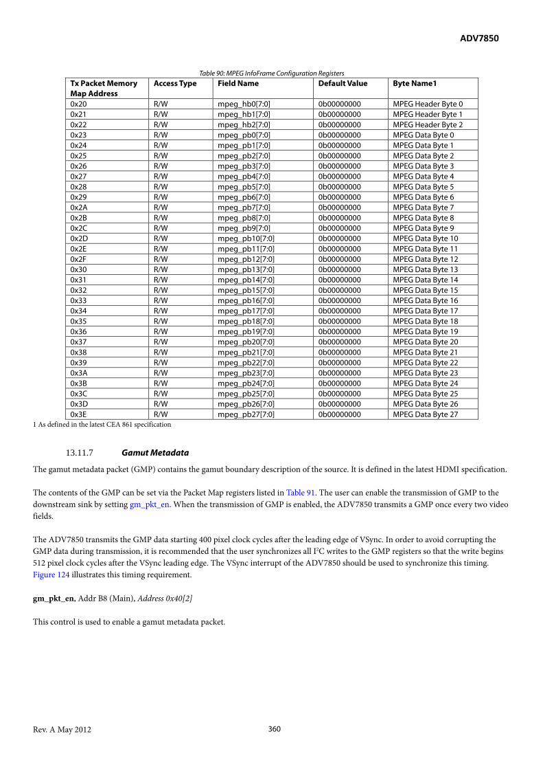
ADV7850
Rev. A May 2012 360
Table 90: MPEG InfoFrame Configuration Registers Tx Packet Memory Map Address
Access Type Field Name Default Value Byte Name1
0x20 R/W mpeg_hb0[7:0] 0b00000000 MPEG Header Byte 0 0x21 R/W mpeg_hb1[7:0] 0b00000000 MPEG Header Byte 1 0x22 R/W mpeg_hb2[7:0] 0b00000000 MPEG Header Byte 2 0x23 R/W mpeg_pb0[7:0] 0b00000000 MPEG Data Byte 0 0x24 R/W mpeg_pb1[7:0] 0b00000000 MPEG Data Byte 1 0x25 R/W mpeg_pb2[7:0] 0b00000000 MPEG Data Byte 2 0x26 R/W mpeg_pb3[7:0] 0b00000000 MPEG Data Byte 3 0x27 R/W mpeg_pb4[7:0] 0b00000000 MPEG Data Byte 4 0x28 R/W mpeg_pb5[7:0] 0b00000000 MPEG Data Byte 5 0x29 R/W mpeg_pb6[7:0] 0b00000000 MPEG Data Byte 6 0x2A R/W mpeg_pb7[7:0] 0b00000000 MPEG Data Byte 7 0x2B R/W mpeg_pb8[7:0] 0b00000000 MPEG Data Byte 8 0x2C R/W mpeg_pb9[7:0] 0b00000000 MPEG Data Byte 9 0x2D R/W mpeg_pb10[7:0] 0b00000000 MPEG Data Byte 10 0x2E R/W mpeg_pb11[7:0] 0b00000000 MPEG Data Byte 11 0x2F R/W mpeg_pb12[7:0] 0b00000000 MPEG Data Byte 12 0x30 R/W mpeg_pb13[7:0] 0b00000000 MPEG Data Byte 13 0x31 R/W mpeg_pb14[7:0] 0b00000000 MPEG Data Byte 14 0x32 R/W mpeg_pb15[7:0] 0b00000000 MPEG Data Byte 15 0x33 R/W mpeg_pb16[7:0] 0b00000000 MPEG Data Byte 16 0x34 R/W mpeg_pb17[7:0] 0b00000000 MPEG Data Byte 17 0x35 R/W mpeg_pb18[7:0] 0b00000000 MPEG Data Byte 18 0x36 R/W mpeg_pb19[7:0] 0b00000000 MPEG Data Byte 19 0x37 R/W mpeg_pb20[7:0] 0b00000000 MPEG Data Byte 20 0x38 R/W mpeg_pb21[7:0] 0b00000000 MPEG Data Byte 21 0x39 R/W mpeg_pb22[7:0] 0b00000000 MPEG Data Byte 22 0x3A R/W mpeg_pb23[7:0] 0b00000000 MPEG Data Byte 23 0x3B R/W mpeg_pb24[7:0] 0b00000000 MPEG Data Byte 24 0x3C R/W mpeg_pb25[7:0] 0b00000000 MPEG Data Byte 25 0x3D R/W mpeg_pb26[7:0] 0b00000000 MPEG Data Byte 26 0x3E R/W mpeg_pb27[7:0] 0b00000000 MPEG Data Byte 27
1 As defined in the latest CEA 861 specification
13.11.7 Gamut Metadata
The gamut metadata packet (GMP) contains the gamut boundary description of the source. It is defined in the latest HDMI specification. The contents of the GMP can be set via the Packet Map registers listed in Table 91. The user can enable the transmission of GMP to the downstream sink by setting gm_pkt_en. When the transmission of GMP is enabled, the ADV7850 transmits a GMP once every two video fields. The ADV7850 transmits the GMP data starting 400 pixel clock cycles after the leading edge of VSync. In order to avoid corrupting the GMP data during transmission, it is recommended that the user synchronizes all I2C writes to the GMP registers so that the write begins 512 pixel clock cycles after the VSync leading edge. The VSync interrupt of the ADV7850 should be used to synchronize this timing. Figure 124 illustrates this timing requirement. gm_pkt_en, Addr B8 (Main), Address 0x40[2] This control is used to enable a gamut metadata packet.

ADV7850
Rev. A May 2012 361
Function gm_pkt_en Description 0 Disable gamut metadata packet 1 Enable gamut metadata packet
Figure 124: I2C Write Timing if GMP Data
Table 91: Gamut Metadata Packet Configuration Registers
Tx Packet Memory Map Address
Access Type Field Name Default Value Byte Name1
0xA0 R/W gmp_hb0[7:0] 0b00000000 Gamut Metadata Header Byte 0 0xA1 R/W gmp_hb1[7:0] 0b00000000 Gamut Metadata Header Byte 1 0xA2 R/W gmp_hb2[7:0] 0b00000000 Gamut Metadata Header Byte 2 0xA3 R/W gmp_pb0[7:0] 0b00000000 Gamut Metadata Data Byte 0 0xA4 R/W gmp_pb1[7:0] 0b00000000 Gamut Metadata Data Byte 1 0xA5 R/W gmp_pb2[7:0] 0b00000000 Gamut Metadata Data Byte 2 0xA6 R/W gmp_pb3[7:0] 0b00000000 Gamut Metadata Data Byte 3 0xA7 R/W gmp_pb4[7:0] 0b00000000 Gamut Metadata Data Byte 4 0xA8 R/W gmp_pb5[7:0] 0b00000000 Gamut Metadata Data Byte 5 0xA9 R/W gmp_pb6[7:0] 0b00000000 Gamut Metadata Data Byte 6 0xAA R/W gmp_pb7[7:0] 0b00000000 Gamut Metadata Data Byte 7 0xAB R/W gmp_pb8[7:0] 0b00000000 Gamut Metadata Data Byte 8 0xAC R/W gmp_pb9[7:0] 0b00000000 Gamut Metadata Data Byte 9 0xAD R/W gmp_pb10[7:0] 0b00000000 Gamut Metadata Data Byte 10 0xAE R/W gmp_pb11[7:0] 0b00000000 Gamut Metadata Data Byte 11 0xAF R/W gmp_pb12[7:0] 0b00000000 Gamut Metadata Data Byte 12 0xB0 R/W gmp_pb13[7:0] 0b00000000 Gamut Metadata Data Byte 13 0xB1 R/W gmp_pb14[7:0] 0b00000000 Gamut Metadata Data Byte 14 0xB2 R/W gmp_pb15[7:0] 0b00000000 Gamut Metadata Data Byte 15 0xB3 R/W gmp_pb16[7:0] 0b00000000 Gamut Metadata Data Byte 16 0xB4 R/W gmp_pb17[7:0] 0b00000000 Gamut Metadata Data Byte 17 0xB5 R/W gmp_pb18[7:0] 0b00000000 Gamut Metadata Data Byte 18 0xB6 R/W gmp_pb19[7:0] 0b00000000 Gamut Metadata Data Byte 19 0xB7 R/W gmp_pb20[7:0] 0b00000000 Gamut Metadata Data Byte 20 0xB8 R/W gmp_pb21[7:0] 0b00000000 Gamut Metadata Data Byte 21 0xB9 R/W gmp_pb22[7:0] 0b00000000 Gamut Metadata Data Byte 22 0xBA R/W gmp_pb23[7:0] 0b00000000 Gamut Metadata Data Byte 23 0xBB R/W gmp_pb24[7:0] 0b00000000 Gamut Metadata Data Byte 24 0xBC R/W gmp_pb25[7:0] 0b00000000 Gamut Metadata Data Byte 25 0xBD R/W gmp_pb26[7:0] 0b00000000 Gamut Metadata Data Byte 26 0xBE R/W gmp_pb27[7:0] 0b00000000 Gamut Metadata Data Byte 27
1 As defined in the latest HDMI specification
Falling edge of last DE of last field Rising edge of first DE of
next field
VSync
400 pixel clocks
GMP sending window
Initiate I2C change after 512 clocks
112 pixel clocks

ADV7850
Rev. A May 2012 362
13.12 AUDIO SETUP
13.12.1 Input Format
The ADV7850 is capable of receiving audio data in I2S, SPDIF, DSD or High Bit Rate (HBR) formats for packetization and transmission over the HDMI output interface. audio_sel[2:0], audio_mode[1:0] and i2sformat[1:0] must be used to configure the Tx core according to the incoming audio input. audio_sel[2:0], Addr B8 (Main), Address 0x0A[6:4] This control is used to select the audio input format.
Function audio_sel[2:0] Description 000 I2S 001 SPDIF 010 One bit audio (DSD) 011 High bit rate (HBR) audio 100 DST
i2sformat[1:0], Addr B8 (Main), Address 0x0C[1:0] This control is used to select the I2S output format.
Function i2sformat[1:0] Description 00 I2S 01 Right justified 10 Left justified 11 AES3 direct mode
audio_mode[1:0], Addr B8 (Main), Address 0x0A[3:2] This control is used to set the audio mode selection. This is used in conjunction with audio_sel and i2sformat.
Function audio_mode[1:0] Description 00 DSD raw mode (DSD case), four streams with BPM encoding (HBR case) 01 DSD raw mode (DSD case), four streams, no BPM encoding (HBR case) 10 SPDIF mode (DSD case), one stream with BPM encoding (HBR case) 11 SPDIF mode (DSD case) one stream, no BPM encoding (HBR case)
Table 92: Valid Configuration for audio_mode[1:0]
audio_input_sel Value audio_mode Value Options
Corresponding Configuration
0b010
0b0x DSD in Raw mode 0b1x DSD in SDIF-3 mode
0b011
0b00 HBR input as 4 streams, with Bi-Phase Mark (BPM) encoding 0b01 HBR input as 4 stream, without BPM encoding 0b10 HBR input as 4 stream, without BPM encoding 0b11 HBR input as 1 stream, without BPM encoding

ADV7850
Rev. A May 2012 363
Table 93: Audio Input Format Summary Input Output
AUDIO_ INPUT_ SEL Value
AUDIO_ MODE Value
I2S_ FORMAT Value
Audio Input Signal
Clock Pins
Encoding ADV7850 Output Pin Mapping
Format Packet Type
0b000 0bXX 0b00 I2S[3:0] SCLK, LRCLK, MCLK1
Normal AUD_IN[4:0] AUD_IN[5] SCLK MCLK
Standard I2S Audio Sample Packet
0b000 0bXX 0b01 I2S[3:0] SCLK, LRCLK, MCLK1
Normal AUD_IN[4:0] AUD_IN[5] SCLK MCLK
Right Justified
Audio Sample Packet
0b000 0bXX 0b10 I2S[3:0] SCLK, LRCLK, MCLK1
Normal AUD_IN[4:0] AUD_IN[5] SCLK MCLK
Left Justified
Audio Sample Packet
0b000 0bXX 0b11 I2S[3:0] SCLK, LRCLK, MCLK1
Normal AUD_IN[4:0] AUD_IN[5] SCLK MCLK
AES3 Direct Audio Sample Packet
0b001 0b00 0bXX SPDIF MCLK1 Biphase Mark
AUD_IN[0] MCLK
IEC60958 or IEC61937
Audio Sample Packet
0b010 0b1X 0bXX DSD[5:0] SCLK Normal AUD_IN[5:0] SCLK
DSD DSD Packet
0b010 0b1X 0bXX DSD[5:0]] SCLK SDIF-3 AUD_IN[5:0] SCLK
DSD DSD Packet
0b011 0b00 0bXX I2S[3:0] MCLK Biphase Mark
AUD_IN[4:0] MCLK
IEC61937 HBR Packet
0b011 0b01 0b00 I2S[3:0] SCLK, MCLK1
Normal AUD_IN[4:0] SCLK MCLK
Standard I2S HBR Packet
0b011 0b01 0b01 I2S[3:0] SCLK, MCLK
Normal AUD_IN[4:0] SCLK MCLK
Right Justified
HBR Packet
0b011 0b01 0b10 I2S[3:0] SCLK, MCLK1
Normal AUD_IN[4:0] SCLK MCLK
Left Justified
HBR Packet
0b011 0b01 0b11 I2S[3:0] SCLK, MCLK1
Normal AUD_IN[4:0] SCLK MCLK
AES3 Direct HBR Packet
0b011 0b10 0bXX SPDIF MCLK Biphase Mark
AUD_IN[0] MCLK
IEC61937 HBR Packet
0b011 0b11 0b00 SPDIF SCLK, MCLK1
Normal AUD_IN[0] SCLK MCLK
Standard I2S HBR Packet
0b011 0b11 0b01 I2S[3:0] SCLK, MCLK1
Normal AUD_IN[4:0] SCLK MCLK
Right Justified
HBR Packet
0b011 0b11 0b10 I2S[3:0] SCLK, MCLK1
Normal AUD_IN[4:0] SCLK MCLK
Left Justified
HBR Packet
0b011 0b11 0b11 I2S[3:0] MCLK Normal AUD_IN[4:0] MCLK
IEC61937 HBR Packet
1 Optional signal
13.12.2 I2S Audio The ADV7850 can accommodate the reception of up to four stereo channels of I2S audio at up to a 192 kHz sampling rate. The number of I2S channels the Tx processes can be selected with audioif_cc[2:0]. The selection of the active I2S channels is done via i2senable[3:0]. The audio sampling frequency of the input stream must be set appropriately via i2s_sf[3:0]. This value is used along with the VIC to determine the pixel repetition factor that the Tx core applies to the video data (refer to Section 13.11.3). The value programmed in i2s_sf[3:0] is also

ADV7850
Rev. A May 2012 364
sent across the TMDS link in the channel status data contained in the Audio Sample packets. The placement of I2S channels into the Audio Sample subpackets defined in the HDMI specification can be specified in the following controls:
• SUBPKT0_L_SRC • SUBPKT0_R_SRC • SUBPKT1_L_SRC • SUBPKT1_R_SRC • SUBPKT2_L_SRC • SUBPKT2_R_SRC • SUBPKT3_L_SRC • SUBPKT3_R_SRC
When these fields are set to their default values, all I2S channels are placed in their respective position (for example, I2S0 left channel in channel 0 left position, I2S3 right channel in channel 3 right position, and so on) but this mapping is completely programmable if desired. The ADV7850 Tx core supports the reception of standard I2S, left-justified, right-justified, and direct AES3 stream formats with a sample word width between 16-bits and 24-bits. The format of the input I2S stream is set via i2sformat[1:0] while the audio sample word width is set via word_length[3:0]. The ADV7850 also supports the reception of an I2S stream in both 64-bit and 32-bit modes, so either 32- or 16-bit clock (that is, the signal input through SCLK pin) edges or cycles per channel are valid. The ADV7850 will adapt to 32- or 64-bit modes automatically, and the current mode can be read in i2s_32bit_mode. Refer to Figure 127 to Figure 131 for timing diagrams for the I2S streams input to the ADV7850. When the ADV7850 is configured to receive a direct AES3 stream, the stream it receives should have IEC60958-like subframes (refer to Figure 125) with the stream formatted as follows:
• Data should be aligned as shown in Figure 125. • Preamble left out as shown in Figure 126. • Parity bit is replaced by the block start flag. The ADV7850 automatically computes the parity bit.
The channel status data collected from audio stream input to the pin aud_in[0] is used in the Audio Sample packets sent by the ADV7850 to the downstream sink. The channel status data can alternatively be programmed by setting cs_bit_override. When cs_bit_override is set to 1, setting ext_audiosf_sel allows the programming of the audio sampling frequency used for the channel status bits while all other channel status data is extracted from the audio stream input to I2S0. The sampling frequency is set via i2s_sf[3:0]. Note: All four stereo channels (aud_in[3:0]) are enabled by setting i2senable[3:0] to 0xF and audioif_cc[2:0] to 0x7. If one stereo channel only is needed, the I2S audio stream data must be input to aud_in[0]. i2senable[3:0] and audioif_cc[2:0] must be set to 1. When ext_audiosf_sel is set to 1, the audio sampling frequency programmed via I2S_SF is used for the determination of the pixel repetition factor. audioif_sf[2:0], Addr B8 (Main), Address 0x74[4:2] This control is used to set the audio sampling frequency in the InfoFrame. It should be set to 0, except for SACD.
Function audioif_sf[2:0] Description 000 Default
audioif_cc[2:0], Addr B8 (Main), Address 0x73[2:0] This control is used to select the audio InfoFrame channel count.

ADV7850
Rev. A May 2012 365
Function audioif_cc[2:0] Description 000 Refer to stream header 001 2 channels 010 3 channels 011 4 channels 100 5 channels 101 6 channels 110 7 channels 111 8 channels
i2senable[3:0], Addr B8 (Main), Address 0x0C[5:2] This control is used to enable the I2S pins.
Function i2senable[3:0] Description 0000 Disable all channels 1111 Enable all channels
i2s_sf[3:0], Addr B8 (Main), Address 0x15[7:4] This control is used to set the sampling frequency for I2S audio. This information is used by both the audio Rx and the pixel repetition.
Function i2s_sf[3:0] Description 0000 44.1 kHz 0001 Reserved 0010 48 kHz 0011 32 kHz 0100 Reserved 0101 Reserved 0110 Reserved 0111 Reserved 1000 88.2 kHz 1001 Reserved 1010 96 kHz 1011 Reserved 1100 176.4 kHz 1101 Reserved 1110 192 kHz 1111 Reserved
subpkt0_l_src[2:0], Addr B8 (Main), Address 0x0E[5:3] This control is used to specify the source of the sub packet 0, left channel.
Function subpkt0_l_src[2:0] Description 000 Default
subpkt0_r_src[2:0], Addr B8 (Main), Address 0x0E[2:0] This control is used to specify the source of the sub packet 0, right channel.
ADV7850
Rev. A May 2012 366
Function subpkt0_r_src[2:0] Description 001 Default
subpkt1_l_src[2:0], Addr B8 (Main), Address 0x0F[5:3] This control is used to specify the source of the sub packet 1, left channel.
Function subpkt1_l_src[2:0] Description 010 Default
subpkt1_r_src[2:0], Addr B8 (Main), Address 0x0F[2:0] This control is used to specify the source of the sub packet 1, right channel.
Function subpkt1_r_src[2:0] Description 011 Default
subpkt2_l_src[2:0], Addr B8 (Main), Address 0x10[5:3] This control is used to specify the source of the sub packet 2, left channel.
Function subpkt2_l_src[2:0] Description 100 Default
subpkt2_r_src[2:0], Addr B8 (Main), Address 0x10[2:0] This control is used to specify the source of the sub packet 2, right channel.
Function subpkt2_r_src[2:0] Description 101 Default
subpkt3_l_src[2:0], Addr B8 (Main), Address 0x11[5:3] This control is used to specify the source of the sub packet 3, left channel.
Function subpkt3_l_src[2:0] Description 110 Default
subpkt3_r_src[2:0], Addr B8 (Main), Address 0x11[2:0] This control is used to specify the source of the sub packet 3, right channel.
Function subpkt3_r_src[2:0] Description 111 Default
i2s_32bit_mode, Addr B8 (Main), Address 0x42[3] (Read Only) This readback indicates the mode of the I2S detected.

ADV7850
Rev. A May 2012 367
Function i2s_32bit_mode Description 0 32-bit mode detected 1 64-bit mode detected
cs_bit_override, Addr B8 (Main), Address 0x0C[6] This control is used to select the source of the channel status bits when using I2S mode.
Function cs_bit_override Description 0 Use channel status bits from I2S stream 1 Use channel status bits from I2C registers
ext_audiosf_sel, Addr B8 (Main), Address 0x0C[7] This control is used to select the sampling frequency for the SPDIF output.
Function ext_audiosf_sel Description 0 Use sampling frequency from I2S stream, for SPDIF stream 1 Use sampling frequency from I2C registers
Figure 125: IEC60958 Sub Stream
Data V U C BLSB
23 24 27
Validity Flag
User Data
Channel Status
Block Start Flag
MSB
0 0 0 0
31
0
31
Figure 126: AES3 Stream Format Input to ADV7850
LRCLK
SCLK
DATA
LEFT RIGHT
LSBMSB MSB LSB
32 Clock Slots 32 Clock Slots
Figure 127: Timing of Standard I2S Stream Input to ADV7850
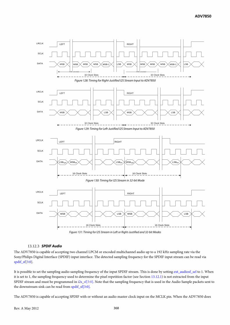
ADV7850
Rev. A May 2012 368
LRCLK
SCLK
DATA
LEFT RIGHT
LSBMSB MSB LSB
32 Clock Slots 32 Clock Slots
MSB MSB MSB MSBMSB-1MSB MSB MSB-1
MSB extended MSB extended
Figure 128: Timing for Right-Justified I2S Stream Input to ADV7850
LRCLK
SCLK
DATA
LEFT RIGHT
LSBMSB MSB LSB
32 Clock Slots 32 Clock Slots
Figure 129: Timing for Left-Justified I2S Stream Input to ADV7850
LRCLK
SCLK
DATA
LEFT RIGHT
LSBleftMSBleft MSBright LSBleft
16 Clock Slots 16 Clock Slots
LSBright
Figure 130: Timing for I2S Stream in 32-bit Mode
LRCLK
SCLK
DATA
LEFT RIGHT
LSBMSB MSB LSB
16 Clock Slots 16 Clock Slots
Figure 131: Timing for I2S Stream in Left or Right-Justified and 32-bit Modes
13.12.3 SPDIF Audio The ADV7850 is capable of accepting two channel LPCM or encoded multichannel audio up to a 192 kHz sampling rate via the Sony/Philips Digital Interface (SPDIF) input interface. The detected sampling frequency for the SPDIF input stream can be read via spdif_sf[3:0]. It is possible to set the sampling audio sampling frequency of the input SPDIF stream. This is done by setting ext_audiosf_sel to 1. When it is set to 1, the sampling frequency used to determine the pixel repetition factor (see Section 13.12.1) is not extracted from the input SPDIF stream and must be programmed in i2s_sf[3:0]. Note that the sampling frequency that is used in the Audio Sample packets sent to the downstream sink can be read from spdif_sf[3:0]. The ADV7850 is capable of accepting SPDIF with or without an audio master clock input on the MCLK pin. When the ADV7850 does

ADV7850
Rev. A May 2012 369
not receive an audio master clock, the ADV7850 uses the bit clock input via the SCLK pin to internally generate an audio master clock and determine the CTS value. spdif_sf[3:0], Addr B8 (Main), Address 0x04[7:4] (Read Only) This readback displays the SPDIF audio sampling frequency decoded by the hardware.
Function spdif_sf[3:0] Description 0000 44.1 kHz 0001 NA 0010 48 kHz 0011 32 kHz 0100 NA 0101 NA 0110 NA 0111 NA 1000 88.2 kHz 1001 NA 1010 96 kHz 1011 NA 1100 176.4 kHz 1101 NA 1110 192 kHz 1111 NA
13.12.4 DSD Audio The ADV7850 uses 1-bit Audio Sample packets to transmit DSD audio data across the HDMI link to the downstream sink. The ADV7850 supports up to six channels of DSD data which can be input onto six data lines clocked by the signal input to DSD_CLK. The ADV7850 can be configured to receive a DSD stream by setting audio_sel[2:0] to 0b010. The mode of the DSD stream input to the ADV7850 can be set via audio_mode[1:0]. The audio sampling frequency must be set via audioif_sf[2:0]. Note the DSD clock input to SCLK has a frequency that is 64 times the audio sampling frequency programmed in audioif_sf[2:0]. Refer to Table 93 for additional details on the DSD modes supported by the ADV7850.
Table 94: Valid Configuration for audioif_sf[2:0] AUDIO_INPUT_SEL Value AUDIOIF_SF Value Options Corresponding Configuration ≠0b010
0b000 Not DSD Audio
0b011
0b001 DSD Audio, 64x32 kHz
0b010 DSD Audio, 64x44.1 kHz 0b011 DSD Audio, 64x48 kHz 0b100 DSD Audio, 64x88.2 kHz
0b101 DSD Audio, 64x96 kHz 0b110 DSD Audio, 64x176.4 kHz 0b111 DSD Audio, 64x192 kHz
13.12.5 HBR Audio The ADV7850 uses an HBR audio packet to transmit across the TMDS link compressed audio streams conforming to IEC 61937 and with a high bit rate (that is, a bit rate higher than 6.144 Mbps). papb_sync can be toggled from 0 to 1 to synchronize the Pa and Pb syncword, which marks the beginning of a stream repetition with the subpacket 0. For data bursts with a repetition period, which is a multiple of four frames, the synchronization will persist. If the data burst does not have a repetition period of four frames, setting papb_sync is not needed but will not have any negative effects. The transition of
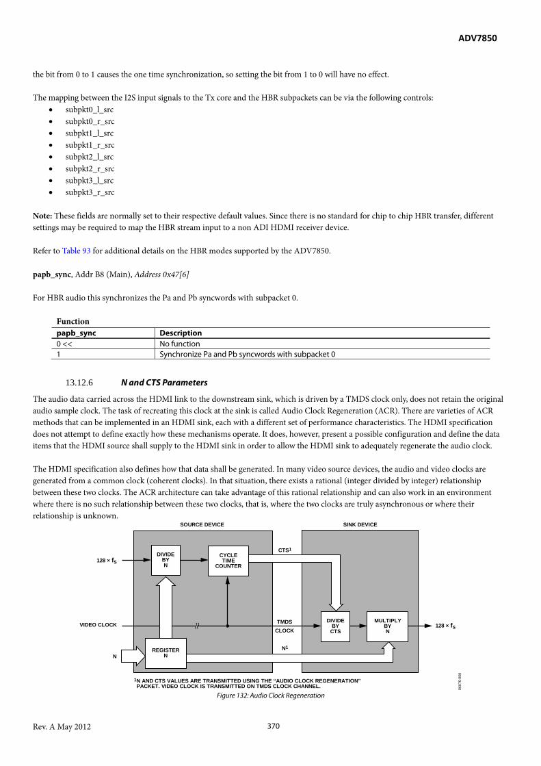
ADV7850
Rev. A May 2012 370
the bit from 0 to 1 causes the one time synchronization, so setting the bit from 1 to 0 will have no effect. The mapping between the I2S input signals to the Tx core and the HBR subpackets can be via the following controls:
• subpkt0_l_src • subpkt0_r_src • subpkt1_l_src • subpkt1_r_src • subpkt2_l_src • subpkt2_r_src • subpkt3_l_src • subpkt3_r_src
Note: These fields are normally set to their respective default values. Since there is no standard for chip to chip HBR transfer, different settings may be required to map the HBR stream input to a non ADI HDMI receiver device. Refer to Table 93 for additional details on the HBR modes supported by the ADV7850. papb_sync, Addr B8 (Main), Address 0x47[6] For HBR audio this synchronizes the Pa and Pb syncwords with subpacket 0.
Function papb_sync Description 0 << No function 1 Synchronize Pa and Pb syncwords with subpacket 0
13.12.6 N and CTS Parameters
The audio data carried across the HDMI link to the downstream sink, which is driven by a TMDS clock only, does not retain the original audio sample clock. The task of recreating this clock at the sink is called Audio Clock Regeneration (ACR). There are varieties of ACR methods that can be implemented in an HDMI sink, each with a different set of performance characteristics. The HDMI specification does not attempt to define exactly how these mechanisms operate. It does, however, present a possible configuration and define the data items that the HDMI source shall supply to the HDMI sink in order to allow the HDMI sink to adequately regenerate the audio clock. The HDMI specification also defines how that data shall be generated. In many video source devices, the audio and video clocks are generated from a common clock (coherent clocks). In that situation, there exists a rational (integer divided by integer) relationship between these two clocks. The ACR architecture can take advantage of this rational relationship and can also work in an environment where there is no such relationship between these two clocks, that is, where the two clocks are truly asynchronous or where their relationship is unknown.
Figure 132: Audio Clock Regeneration
DIVIDEBYN
DIVIDEBY
CTS
CTS1
N1
TMDSCLOCK
VIDEO CLOCK
N
128 × fS
128 × fS
SINK DEVICESOURCE DEVICE
1N AND CTS VALUES ARE TRANSMITTED USING THE “AUDIO CLOCK REGENERATION”PACKET. VIDEO CLOCK IS TRANSMITTED ON TMDS CLOCK CHANNEL.
REGISTERN
MULTIPLYBYN
CYCLETIME
COUNTER
0607
6-00
8
ADV7850
Rev. A May 2012 371
Figure 132 illustrates the overall system architecture model used by HDMI devices for audio clock regeneration. The HDMI source determines the fractional relationship between the video clock and an audio reference clock (128*fs) and passes the numerator and denominator for that fraction to the sink across the HDMI link. The sink may then recreate the audio clock from the TMDS clock by using a clock divider and a clock multiplier. The exact relationship between the two clocks is shown in Equation 13.
CTSNff CLKTMDSs _128 =
Equation 13: Relationship Between Audio Reference and TMDS Clocks
The source determines the value of the numerator N as specified in the HDMI specification. Typically, this value N is used in a clock divider to generate an intermediate clock that is slower than the 128*fs clock by the factor N. The source typically determines the value of the denominator Cycle Time Stamp (CTS) by counting the number of TMDS clocks in each of the 128*fs/N clocks.
13.12.7 N Parameter N is an integer number and is calculated using Equation 14 with the recommended optimal value shown in Equation 15 which approximately equals N for coherent audio and video clock sources. Table 95 to Table 97 can be used to determine the value of N. For non coherent sources or sources where coherency is not known, Equation 14, Equation 15, and Equation 16 should be used.
128*fs/1500Hz ≤N ≤128*fs/300Hz Equation 14: Restriction for N Value
128*fs/1000Hz
Equation 15: Optimal N Value
13.12.8 CTS Parameter The CTS is an integer number that satisfies Equation 16.
s
CLKTMDSAverage f
NfCTS
128_=
Equation 16: Relationship Between N and CTS
13.12.9 Recommended N and Expected CTS Values The recommended values of N for several standard pixel clocks are provided in Table 95 to Table 97. The ADV7850 has two modes for CTS generation. Manual mode: Manual mode is selected by setting cts_sel to 1. In manual mode, the user can program the CTS number directly into the chip via cts_manual[19:0]. Manual mode is suitable for coherent audio and video, where the audio and video clocks are generated from the same crystal. Thus, CTS should be a fixed number. Automatic mode: Automatic mode is selected by setting cts_sel to 0. In automatic mode, the chip computes the CTS based on the actual audio and video rates. The result can be read from cts_internal. Automatic mode is good for incoherent audio or video, where there is no simple integer ratio between the audio and video clock. The 20-bit N value used by the Tx core of the ADV7850 can be programmed in the field N. cts_sel, Addr B8 (Main), Address 0x0A[7] This control is used to select the CTS option; either internally generated CTS values or external user-defined CTS.

ADV7850
Rev. A May 2012 372
Function cts_sel Description 0 Internally generated 1 Set by user
cts_manual[19:0], Addr 72 (Main), Address 0x07[3:0]; Address 0x08[7:0]; Address 0x09[7:0] Cycle Time Stamp (CTS) manually set. This parameter is used with the N parameter to regenerate the audio clock in the receiver.
Function cts_manual[19:0] Description 0x00000 << Default value
cts_internal[19:0] , Addr 72 (Main), Address 0x04[3:0]; Address 0x05[7:0]; Address 0x06[7:0] (Read Only) Automatically generated Cycle Time Stamp (CTS) parameter. This parameter is used with the N parameter to regenerate the audio clock in the receiver.
Function cts_internal[19:0] Description 0x00000 << Default value
n[19:0], Main Map, Address 0x01[3:0]; Address 0x02[7:0]; Address 0x03[7:0] Audio clock regeneration parameter N. This parameter is used with CTS to regenerate the audio clock in the receiver.
Function n[19:0] Description 0x00000 << Default value
Table 95: Recommended N and Expected CTS Values for 32 kHz Audio
32 kHz Pixel Clock (MHz) N CTS 25.2/1.001 4576 28125 25.2 4096 25200 27 4096 27000 27*1.001 4096 27027 54 4096 54000 54*1.001 4096 54054 74.25/1.001 11648 210937 – 210938 74.25 4096 74250 148.5/1.001 11648 421875 148.5 4096 148500 Other 4096 Measured
Table 96: Recommended N and Expected CTS Values for 44.1 kHz and Multiples
44.1kHz 88.2 kHz 176.4 kHz Pixel Clock (MHz) N CTS N CTS N CTS 25.2/1.001 7007 31250 14014 31250 28028 31250 25.2 6272 28000 12544 28000 25088 28000 27 6272 30000 12544 30000 25088 30000 27*1.001 6272 30030 12544 30030 25088 30030 54 6272 60000 12544 60000 25088 60000 54*1.001 6272 60060 12544 60060 25088 60060 74.25/1.001 17836 234375 35672 234375 71344 234375 74.25 6272 82500 12544 82500 25088 82500 148.5/1.001 8918 234375 17836 234375 35672 234375
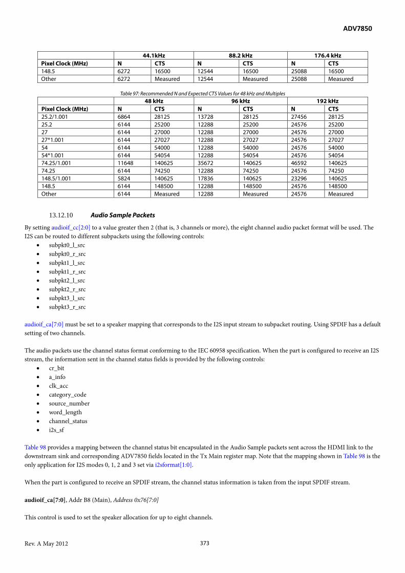
ADV7850
Rev. A May 2012 373
44.1kHz 88.2 kHz 176.4 kHz Pixel Clock (MHz) N CTS N CTS N CTS 148.5 6272 16500 12544 16500 25088 16500 Other 6272 Measured 12544 Measured 25088 Measured
Table 97: Recommended N and Expected CTS Values for 48 kHz and Multiples
48 kHz 96 kHz 192 kHz Pixel Clock (MHz) N CTS N CTS N CTS 25.2/1.001 6864 28125 13728 28125 27456 28125 25.2 6144 25200 12288 25200 24576 25200 27 6144 27000 12288 27000 24576 27000 27*1.001 6144 27027 12288 27027 24576 27027 54 6144 54000 12288 54000 24576 54000 54*1.001 6144 54054 12288 54054 24576 54054 74.25/1.001 11648 140625 35672 140625 46592 140625 74.25 6144 74250 12288 74250 24576 74250 148.5/1.001 5824 140625 17836 140625 23296 140625 148.5 6144 148500 12288 148500 24576 148500 Other 6144 Measured 12288 Measured 24576 Measured
13.12.10 Audio Sample Packets
By setting audioif_cc[2:0] to a value greater then 2 (that is, 3 channels or more), the eight channel audio packet format will be used. The I2S can be routed to different subpackets using the following controls:
• subpkt0_l_src • subpkt0_r_src • subpkt1_l_src • subpkt1_r_src • subpkt2_l_src • subpkt2_r_src • subpkt3_l_src • subpkt3_r_src
audioif_ca[7:0] must be set to a speaker mapping that corresponds to the I2S input stream to subpacket routing. Using SPDIF has a default setting of two channels. The audio packets use the channel status format conforming to the IEC 60958 specification. When the part is configured to receive an I2S stream, the information sent in the channel status fields is provided by the following controls:
• cr_bit • a_info • clk_acc • category_code • source_number • word_length • channel_status • i2s_sf
Table 98 provides a mapping between the channel status bit encapsulated in the Audio Sample packets sent across the HDMI link to the downstream sink and corresponding ADV7850 fields located in the Tx Main register map. Note that the mapping shown in Table 98 is the only application for I2S modes 0, 1, 2 and 3 set via i2sformat[1:0]. When the part is configured to receive an SPDIF stream, the channel status information is taken from the input SPDIF stream. audioif_ca[7:0], Addr B8 (Main), Address 0x76[7:0] This control is used to set the speaker allocation for up to eight channels.

ADV7850
Rev. A May 2012 374
Function audioif_ca[7:0] Description 00000000 Default
cr_bit, Addr B8 (Main), Address 0x12[5] This control is used to set the copyright protection.
Function cr_bit Description 0 Copyright 1 Not copyright protected
a_info[2:0], Addr B8 (Main), Address 0x12[4:2] This control is used to select the pre-emphasis on the audio output channels. Refer to IEC 60958 for more details.
Function a_info[2:0] Description 000 Two audio channels without pre-emphasis 001 Two audio channels with 50/15 uS pre-emphasis 010 Reserved 011 Reserved 100 Not described 101 Not described 110 Not described 111 Not described
clk_acc[1:0], Addr B8 (Main), Address 0x12[1:0] This control is used to set the clock accuracy.
Function clk_acc[1:0] Description 00 Level II - normal accuracy +/-1000 x 10^-6 01 Level I - high accuracy +/- 50 x 10^-6 10 Level III - variable pitch shifted clock 11 Reserved
category_code[7:0], Addr B8 (Main), Address 0x13[7:0] This control is used to set the category code for the audio InfoFrame.
Function category_code[7:0] Description 00000000 Default
source_number[3:0], Addr B8 (Main), Address 0x14[7:4] This control is used to set the source number.

ADV7850
Rev. A May 2012 375
Function source_number[3:0] Description 0000 Default
word_length[3:0], Addr B8 (Main), Address 0x14[3:0] This control is used to set the word length.
Function word_length[3:0] Description 0000 Not specified 0001 Not specified 0010 16 bits 0011 20 bits 0100 18 bits 0101 22 bits 0110 Reserved 0111 Reserved 1000 19 bits 1001 23 bits 1010 20 bits 1011 24 bits 1100 17 bits 1101 21 bits 1110 Reserved 1111 Reserved
cs_bit_1_0[1:0], Addr B8 (Main), Address 0x12[7:6] This control is used to set the channel status bits[0] and [1]. Bit 0 = 0 indicates consumer use. Bit 1 = 0 indicates LPCM audio.
Function cs_bit_1_0[1:0] Description 00 Default
Table 98: I2S Channel Status ADV7850 Register Map Location of Fixed Value
Channel Status Bit
Channel Status Bit Name Main Map Bit Main Map Bit Name or Fixed Value
0 Consumer use 0x12[6] channel_status[0] 1 Audio sample word 0x12[7] channel_status[1] 2 Copyright 0x12[5] cr_bit 3 Emphasis 0x12[2] a_info[0] 4 Emphasis 0x12[3] a_info[1] 5 Emphasis 0x12[4] a_info[2] 6 Mode 0 0 7 Mode 0 0 8 Category code 0x13[0] category_code[0] 9 Category code 0x13[1] category_code[1] 10 Category code 0x13[2] category_code[2] 11 Category code 0x13[3] category_code[3] 12 Category code 0x13[4] category_code[4] 13 Category code 0x13[5] category_code[5] 14 Category code 0x13[6] category_code[6] 15 Category code 0x13[7] category_code[7] 16 Source number 0x14[4] source_number[0] 17 Source number 0x14[5] source_number[1] 18 Source number 0x14[6] source_number[2] 19 Source number 0x14[7] source_number[3] 20 Channel number See Figure 133 See Figure 133

ADV7850
Rev. A May 2012 376
Channel Status Bit
Channel Status Bit Name Main Map Bit Main Map Bit Name or Fixed Value
21 Channel number See Figure 133 See Figure 133 22 Channel number See Figure 133 See Figure 133 23 Channel number See Figure 133 See Figure 133 24 Sampling frequency 0x15[4] i2s_sf[0] 25 Sampling frequency 0x15[5] i2s_sf[1] 26 Sampling frequency 0x15[6] i2s_sf[2] 27 Sampling frequency 0x15[7] i2s_sf[3] 28 Clock accuracy 0x12[0] clk_acc[0] 29 Clock accuracy 0x12[1] clk_acc[1] 30 Not Defined 0 0 31 Not Defined 0 0 32 Word length 0x14[0] word_length[0] 33 Word length 0x14[1] word_length[1] 34 Word length 0x14[2] word_length[2] 35 Word length 0x14[3] word_length[3] 36 Original sampling frequency 0 0 37 Original sampling frequency 0 0 38 Original sampling frequency 0 0 39 Original sampling frequency 0 0 40 CGMS-A 0 0 41 CGMS-A 0 0 42-191 Not Defined 0 0
Figure 133 shows how the channel number bits 20 to 23 are set, based on the layout bit and sample_present.spx bit, which indicate if subpacket x contains audio samples(s). The layout bit in the Audio Sample packet header and the sample_present.spx bit are determined based on the values programmed in audioif_cc[2:0]. For example, if audioif_cc[2:0] is set to 0b001, which indicates stereo audio, the layout bit will be zero and all Audio Sample subpackets will contain information for channels 1 and 2. If audioif_cc[2:0] is set to 0b011, indicating four channels, the layout bit is set to 1; sample_present.sp0 is set to 1, sample_present.sp1 is set to 1, and sample_present_sp2 is set to 0.

ADV7850
Rev. A May 2012 377
Figure 133: Definition of Channel Status Bits 20 to 23
13.12.11 Audio InfoFrame
The audio InfoFrame allows the sink to identify the characteristics of an audio stream before the channel status information is available. The ADV7850 can be configured to transmit audio InfoFrame by setting audioif_pkt_en to 1. When the transmission of audio InfoFrame is enabled, the ADV7850 transmits an audio InfoFrame once every two video fields. Table 99 provides a list of the registers that can be used to configure audio InfoFrames. audioif_pkt_en, Addr B8 (Main), Address 0x44[3] This control is used to enable an audio InfoFrame.
Function audioif_pkt_en Description 0 Disable audio InfoFrame 1 Enable audio InfoFrame
Au d i o Sa mp l e Pa cke t H e a d e r L a yo u t b i t
1
0
Au d i o Sa mp l e Pa cke t H e a d e r sa mp l e _ p re se n t . sp X b i t
Au d i o Sa mp l e Su b p a cke t X C l [ 2 3 : 2 0 ] = 2 ( X ) + 1 C r [ 2 3 : 2 0 ] = 2 ( X ) + 2
Au d i o Sa mp l e Su b p a cke t X C l [ 2 3 : 2 0 ] = 1 C r [ 2 3 : 2 0 ] = 2
Au d i o Sa mp l e Pa cke t H e a d e r sa mp l e _ p re se n t . sp X b i t
S t a r t
1 1
0
Au d i o Sa mp l e Su b p a cke t X N o t Pre se n t

ADV7850
Rev. A May 2012 378
Table 99: Audio InfoFrame Configuration Registers HDMI Tx Main Map Address
Bit Location Access Type Default Value Field or Byte Name1
0x70 [2:0] R/W 0b001 Audio InfoFrame InfoFrame version number 0x71 [4:0] R/W 0b01010 Audio InfoFrame InfoFrame length 0x72 [7:0] R/W 0b00000000 Audio InfoFrame Checksum2 0x73 [7:0] R/W 0b00000000 Audio InfoFrame Data Byte 1 0x74 [7:0] R/W 0b00000000 Audio InfoFrame Data Byte 2 0x75 [7:0] R/W 0b00000000 Audio InfoFrame Data Byte 3 0x76 [7:0] R/W 0b00000000 Audio InfoFrame Data Byte 4 0x77 [7:0] R/W 0b00000000 Audio InfoFrame Data Byte 5 0x78 [7:0] R/W 0b00000000 Audio InfoFrame Data Byte 6 0x79 [7:0] R/W 0b00000000 Audio InfoFrame Data Byte 7 0x7A [7:0] R/W 00000000 Audio InfoFrame Data Byte 8 0x7B [7:0] R/W 00000000 Audio InfoFrame Data Byte 9 0x7C [7:0] R/W 00000000 Audio InfoFrame Data Byte 10
1 As defined in the latest CEA 861 specification 2. Only used when auto_checksum_en = 0
13.12.12 Audio Content Protection Packet
The Audio Content Protection (ACP) packet is used for transmitting content related information about the active audio stream. Use of the ACP packet is defined in the license agreement of the protected audio stream. The contents of the ACP packet can be set via the set of Packet Map registers listed in Table 100. The user can enable the transmission of an ACP packet to the downstream sink by setting acp_pkt_en to 1. When the transmission of ACP packets is enabled, the ADV7850 transmits an APC packets once every two video fields. acp_pkt_en, Addr B8 (Main), Address 0x40[4] This control is used to enable an ACP packet.
Function acp_pkt_en Description 0 Disable ACP packet 1 Enable ACP packet
Table 100: ACP Packet Configuration Registers
HDMI Tx Packet Map Address
Access Type Field Name Default Value Byte Name1
0x40 R/W acp_hb0[7:0] 0b00000000 ACP Header Byte 0 0x41 R/W acp_hb1[7:0] 0b00000000 ACP Header Byte 1 0x42 R/W acp_hb2[7:0] 0b00000000 ACP Header Byte 2 0x43 R/W acp_pb0[7:0] 0b00000000 ACP Data Byte 0 0x44 R/W acp_pb1[7:0] 0b00000000 ACP Data Byte 1 0x45 R/W acp_pb2[7:0] 0b00000000 ACP Data Byte 2 0x46 R/W acp_pb3[7:0] 0b00000000 ACP Data Byte 3 0x47 R/W acp_pb4[7:0] 0b00000000 ACP Data Byte 4 0x48 R/W acp_pb5[7:0] 0b00000000 ACP Data Byte 5 0x49 R/W acp_pb6[7:0] 0b00000000 ACP Data Byte 6 0x4A R/W acp_pb7[7:0] 0b00000000 ACP Data Byte 7 0x4B R/W acp_pb8[7:0] 0b00000000 ACP Data Byte 8 0x4C R/W acp_pb9[7:0] 0b00000000 ACP Data Byte 9 0x4D R/W acp_pb10[7:0] 0b00000000 ACP Data Byte 10 0x4E R/W acp_pb11[7:0] 0b00000000 ACP Data Byte 11 0x4F R/W acp_pb12[7:0] 0b00000000 ACP Data Byte 12 0x50 R/W acp_pb13[7:0] 0b00000000 ACP Data Byte 13 0x51 R/W acp_pb14[7:0] 0b00000000 ACP Data Byte 14 0x52 R/W acp_pb15[7:0] 0b00000000 ACP Data Byte 15 0x53 R/W acp_pb16[7:0] 0b00000000 ACP Data Byte 16
ADV7850
Rev. A May 2012 379
HDMI Tx Packet Map Address
Access Type Field Name Default Value Byte Name1
0x54 R/W acp_pb17[7:0] 0b00000000 ACP Data Byte 17 0x55 R/W acp_pb18[7:0] 0b00000000 ACP Data Byte 18 0x56 R/W acp_pb19[7:0] 0b00000000 ACP Data Byte 19 0x57 R/W acp_pb20[7:0] 0b00000000 ACP Data Byte 20 0x58 R/W acp_pb21[7:0] 0b00000000 ACP Data Byte 21 0x59 R/W acp_pb22[7:0] 0b00000000 ACP Data Byte 22 0x5A R/W acp_pb23[7:0] 0b00000000 ACP Data Byte 23 0x5B R/W acp_pb24[7:0] 0b00000000 ACP Data Byte 24 0x5C R/W acp_pb25[7:0] 0b00000000 ACP Data Byte 25 0x5D R/W acp_pb26[7:0] 0b00000000 ACP Data Byte 26 0x5E R/W acp_pb27[7:0] 0b00000000 ACP Data Byte 27
1 As defined in the latest CEA 861 specification
13.12.13 ISRC Packet
If SUPPORTS_AI in the Vendor Specific Data Block (VSDB) of the sink EDID is set to 1, the International Standard Recording Code (ISRC) packets 1 and 2 can be transmitted. The ADV7850 can be configured to transmit ISRC packet by setting isrc_pkt_en to 1. When the transmission of an ISRC packet is enabled, the ADV7850 transmits an ISRC packet once every two video fields. Table 101 and Table 102 provide a list of the registers that can be used to configure ISRC packets. isrc_pkt_en, Addr B8 (Main), Address 0x40[3] This control is used to enable an ISRC packet.
Function isrc_pkt_en Description 0 Disable ISRC packet 1 Enable ISRC packet
Table 101: ISRC1 Packet Configuration Registers
HDMI Tx Packet Map Address
Access Type Field Name Default Value Byte Name1
0x60 R/W isrc1_hb0[7:0] 0b00000000 ISRC1 Header Byte 0 0x61 R/W isrc1_hb1[7:0] 0b00000000 ISRC1 Header Byte 1 0x62 R/W isrc1_hb2[7:0] 0b00000000 ISRC1 Header Byte 2 0x63 R/W isrc1_pb0[7:0] 0b00000000 ISRC1 Data Byte 0 0x64 R/W isrc1_pb1[7:0] 0b00000000 ISRC1 Data Byte 1 0x65 R/W isrc1_pb2[7:0] 0b00000000 ISRC1 Data Byte 2 0x66 R/W isrc1_pb3[7:0] 0b00000000 ISRC1 Data Byte 3 0x67 R/W isrc1_pb4[7:0] 0b00000000 ISRC1 Data Byte 4 0x68 R/W isrc1_pb5[7:0] 0b00000000 ISRC1 Data Byte 5 0x69 R/W isrc1_pb6[7:0] 0b00000000 ISRC1 Data Byte 6 0x6A R/W isrc1_pb7[7:0] 0b00000000 ISRC1 Data Byte 7 0x6B R/W isrc1_pb8[7:0] 0b00000000 ISRC1 Data Byte 8 0x6C R/W isrc1_pb9[7:0] 0b00000000 ISRC1 Data Byte 9 0x6D R/W isrc1_pb10[7:0] 0b00000000 ISRC1 Data Byte 10 0x6E R/W isrc1_pb11[7:0] 0b00000000 ISRC1 Data Byte 11 0x6F R/W isrc1_pb12[7:0] 0b00000000 ISRC1 Data Byte 12 0x70 R/W isrc1_pb13[7:0] 0b00000000 ISRC1 Data Byte 13 0x71 R/W isrc1_pb14[7:0] 0b00000000 ISRC1 Data Byte 14 0x72 R/W isrc1_pb15[7:0] 0b00000000 ISRC1 Data Byte 15 0x73 R/W isrc1_pb16[7:0] 0b00000000 ISRC1 Data Byte 16 0x74 R/W isrc1_pb17[7:0] 0b00000000 ISRC1 Data Byte 17 0x75 R/W isrc1_pb18[7:0] 0b00000000 ISRC1 Data Byte 18 0x76 R/W isrc1_pb19[7:0] 0b00000000 ISRC1 Data Byte 19 0x77 R/W isrc1_pb20[7:0] 0b00000000 ISRC1 Data Byte 20

ADV7850
Rev. A May 2012 380
HDMI Tx Packet Map Address
Access Type Field Name Default Value Byte Name1
0x78 R/W isrc1_pb21[7:0] 0b00000000 ISRC1 Data Byte 21 0x79 R/W isrc1_pb22[7:0] 0b00000000 ISRC1 Data Byte 22 0x7A R/W isrc1_pb23[7:0] 0b00000000 ISRC1 Data Byte 23 0x7B R/W isrc1_pb24[7:0] 0b00000000 ISRC1 Data Byte 24 0x7C R/W isrc1_pb25[7:0] 0b00000000 ISRC1 Data Byte 25 0x7D R/W isrc1_pb26[7:0] 0b00000000 ISRC1 Data Byte 26 0x7E R/W isrc1_pb27[7:0] 0b00000000 ISRC1 Data Byte 27
1 As defined in the latest CEA 861 specification
Table 102: ISRC2 Packet Configuration Registers Packet Map Address
Access Type Field Name Default Value Byte Name1
0x80 R/W isrc2_hb0[7:0] 0b00000000 ISRC2 Header Byte 0 0x81 R/W isrc2_hb1[7:0] 0b00000000 ISRC2 Header Byte 1 0x82 R/W isrc2_hb2[7:0] 0b00000000 ISRC2 Header Byte 2 0x83 R/W isrc2_pb0[7:0] 0b00000000 ISRC2 Data Byte 0 0x84 R/W isrc2_pb1[7:0] 0b00000000 ISRC2 Data Byte 1 0x85 R/W isrc2_pb2[7:0] 0b00000000 ISRC2 Data Byte 2 0x86 R/W isrc2_pb3[7:0] 0b00000000 ISRC2 Data Byte 3 0x87 R/W isrc2_pb4[7:0] 0b00000000 ISRC2 Data Byte 4 0x88 R/W isrc2_pb5[7:0] 0b00000000 ISRC2 Data Byte 5 0x89 R/W isrc2_pb6[7:0] 0b00000000 ISRC2 Data Byte 6 0x8A R/W isrc2_pb7[7:0] 0b00000000 ISRC2 Data Byte 7 0x8B R/W isrc2_pb8[7:0] 0b00000000 ISRC2 Data Byte 8 0x8C R/W isrc2_pb9[7:0] 0b00000000 ISRC2 Data Byte 9 0x8D R/W isrc2_pb10[7:0] 0b00000000 ISRC2 Data Byte 10 0x8E R/W isrc2_pb11[7:0] 0b00000000 ISRC2 Data Byte 11 0x8F R/W isrc2_pb12[7:0] 0b00000000 ISRC2 Data Byte 12 0x90 R/W isrc2_pb13[7:0] 0b00000000 ISRC2 Data Byte 13 0x91 R/W isrc2_pb14[7:0] 0b00000000 ISRC2 Data Byte 14 0x92 R/W isrc2_pb15[7:0] 0b00000000 ISRC2 Data Byte 15 0x93 R/W isrc2_pb16[7:0] 0b00000000 ISRC2 Data Byte 16 0x94 R/W isrc2_pb17[7:0] 0b00000000 ISRC2 Data Byte 17 0x95 R/W isrc2_pb18[7:0] 0b00000000 ISRC2 Data Byte 18 0x96 R/W isrc2_pb19[7:0] 0b00000000 ISRC2 Data Byte 19 0x97 R/W isrc2_pb20[7:0] 0b00000000 ISRC2 Data Byte 20 0x98 R/W isrc2_pb21[7:0] 0b00000000 ISRC2 Data Byte 21 0x99 R/W isrc2_pb22[7:0] 0b00000000 ISRC2 Data Byte 22 0x9A R/W isrc2_pb23[7:0] 0b00000000 ISRC2 Data Byte 23 0x9B R/W isrc2_pb24[7:0] 0b00000000 ISRC2 Data Byte 24 0x9C R/W isrc2_pb25[7:0] 0b00000000 ISRC2 Data Byte 25 0x9D R/W isrc2_pb26[7:0] 0b00000000 ISRC2 Data Byte 26 0x9E R/W isrc2_pb27[7:0] 0b00000000 ISRC2 Data Byte 27
1 As defined in the latest CEA 861 specification
13.13 EDID HANDLING
13.13.1 Reading the EDID
The Tx core of the ADV7850 features an EDID/HDCP controller that can read the EDID content of the downstream sink through the DDC lines, TX_DDC_SCL and TX_DDC_SDA. This EDID/HDCP controller begins buffering segment 0 of the downstream sink EDID once the sink hot plug detect (HPD) is detected and the Tx core of the ADV7850 is powered up. The system can request additional segments by programming the EDID segment pointer edid_segment[7:0]. The interrupt edid_ready_interrupt (refer to Section 13.9) indicates that a 256-byte EDID read has been completed, and the EDID content can be read from the EDID Map. edid_segment[7:0], Addr B8 (Main), Address 0xC4[7:0] Sets the E-DDC segment used by the EDID Fetch routine.

ADV7850
Rev. A May 2012 381
13.13.2 EDID Definitions
Extended EDID (E-EDID) supports up to 256 segments. A segment is a 256-byte segment of EDID data containing one or two 128-byte EDID blocks. A typical HDMI sink will have only two EDID blocks and so will only use segment 0. The first EDID block is always a base EDID structure defined in the VESA EDID specifications; the second EDID block is usually the CEA extension defined in the CEA-861 specification. The ADV7850 has a single memory location used to store EDID and HDCP information read from the downstream sink. During HDCP repeater initialization, the EDID data read from the sink is overwritten with HDCP information which is also read from the sink. The sink EDID is not reread after HDCP initialization. The user can request the ADV7850 to rebuffer an EDID segment by using edid_read_en.
13.13.3 Additional Segments
The EDID block 0 byte number 0x7E tells how many additional EDID blocks are available. If byte 0x7E is greater than 1, additional EDID segments need to be read. If there is more than one segment, the second block (that is, block 1) is required to be an EDID extension map. This map should be parsed according to the VESA EDID specification to determine where additional EDID blocks are stored in the sink EDID storage device (that is, EEPROM, RAM, and so on). The ADV7850 is capable of accessing up to 256 segments from EDID of the sink as allowed by the EDID specification. By writing the desired segment number to edid_segment[7:0], the ADV7850 will automatically access the correct portion of the sink EDID over the Tx DDC lines and load the 256 bytes into the EDID/HDCP memory. When the action is complete, the ADV7850 triggers the edid_ready_int interrupt. The EDID data read from the sink can then be accessed from the Tx EDID Map. If the host controller needs access to previously requested EDID information, then it can be stored in its own memory. Figure 134 shows how to implement software to read EDID from the downstream sink using the ADV7850.
Power up Tx via SYSTEM_PD
START
Wait for HPD interrupt HDP_INT
Wait for EDID Ready Interrupt
EDID_READY_INT
Read EDID data from TX EDID
Map
Parse EDID Data
Need Additional Blocks?
Set EDID_SEGMENT desired Segment
Disable EDID Interrupt
EDID_READY_INTuntil next HPD
Setup Audio and Video
YES
NO
Figure 134: Reading Sink EDID Through ADV7850

ADV7850
Rev. A May 2012 382
13.13.4 EDID_TRIES Control
edid_trys[3:0] can be used to set the number of times the Tx EDID/HDCP controller tries to read the sink EDID after a failure. Each time an EDID read fails with an I2C Not Acknowledged (NACK), this value of edid_trys[3:0] is decremented. Once edid_trys[3:0] reaches the value 0, the Tx EDID/HDCP controller will not attempt to read the EDID until edid_trys[3:0] is set to a value other than 0. This could be used if a sink asserts high its HPD signal before the DDC bus is ready, resulting in several NACKs as the ADV7850 attempts to read the EDID. edid_trys[3:0], Addr B8 (Main), Address 0xC9[3:0] This control is used to set the maximum number of times that the EDID read will be attempted if unsuccessful. Reading the EDID begins upon setting this register and on powerup.
Function edid_trys[3:0] Description 0011 Default
13.13.5 EDID_REREAD Control
If the EDID data from the sink is read in and the host determines that the data needs to be reread, edid_read_en can be set from 0 to 1, and the current segment set via edid_segment[7:0] will be reread. Rereading the sink EDID may be useful, for example, if the host finds that one EDID checksum read from the sink is invalid. Note: It is also possible to reread the EDID from the sink by toggling the Tx core power-down system_pd bit from 0 to 1. edid_read_en, Addr B8 (Main), Address 0xC9[4] Reread the current segment if toggled from 0 to 1 for 10 times consecutively.
Function edid_read_en Description 0 << Default value 1 Request the EDID/HDCP controller to read the EDID
13.14 HDCP HANDLING
13.14.1 One Sink And No Upstream Devices
The ADV7850 has a built-in controller, the Tx EDID/HDCP controller, which handles HDCP transmitter states, including handling downstream HDCP repeaters. To activate HDCP from a system level, the host controller needs to set hdcp_desired to 1 and enc_on to 1. This informs the ADV7850 that the video stream it outputs should be encrypted. The ADV7850 takes control from there and implements all the remaining tasks defined by the HDCP 1.4 specification. Before sending audio and video, the BKSV of the downstream sink should be compared with the revocation list compiled by managing System Renewability Messages (SRMs) provided on the source content (for example. DVD, Blue-ray Disc), and the bksv_flag_intr interrupt should be cleared. After the HDCP link is established between the ADV7850 and the downstream sink, the system controller should monitor the status of HDCP by reading enc_on every two seconds. The Tx EDID/HDCP controller error interrupt activates and hdcp_error_interrupt is set to 1 if there is an error relating to the controller. The meaning of the error can be determined by checking hdcp_controller_error[3:0]. bksv_flag_intr, Addr 72 (Main), Address 0x97[6] BKSV Flag interrupt status

ADV7850
Rev. A May 2012 383
Function bksv_flag_intr Description 0 << Interrupt not active 1 Interrupt active. The KSVs from the downstream sink have been read and available in the
Memory Map hdcp_desired, Addr B8 (Main), Address 0xAF[7] This control is used to enable input A/V content encryption.
Function hdcp_desired Description 0 Do not encrypt A/V content 1 Encrypt A/V content
frame_enc, Addr B8 (Main), Address 0xAF[4] This control is used to enable encryption on the current frame.
Function frame_enc Description 0 Do not encrypt current frame 1 Encrypt current frame
bksv0[7:0], Addr B8 (Main), Address 0xBF[7:0] (Read Only) This readback indicates the Bksv read from Rx by the HDCP controller. bksv1[7:0], Addr B8 (Main), Address 0xC0[7:0] (Read Only) This readback indicates the Bksv read from Rx by the HDCP controller. bksv2[7:0], Addr B8 (Main), Address 0xC1[7:0] (Read Only) This readback indicates the Bksv read from Rx by the HDCP controller. bksv3[7:0], Addr B8 (Main), Address 0xC2[7:0] (Read Only) This readback indicates the Bksv read from Rx by the HDCP controller. bksv4[7:0], Addr B8 (Main), Address 0xC3[7:0] (Read Only) This readback indicates the Bksv read from Rx by the HDCP controller. enc_on, Addr B8 (Main), Address 0xB8[6] (Read Only) This readback indicates if the A/V content is being encrypted at present.
Function enc_on Description 0 Not encrypted 1 Encrypted

ADV7850
Rev. A May 2012 384
13.14.2 Multiple Sinks and No Upstream Devices
When connecting the ADV7850 as a source to an HDMI input of a repeater, it is necessary to read all BKSVs from downstream devices. These BKSVs must be checked against a revocation list, which will be provided on the source content. bksv_count[6:0] will be set to 0 when the first BKSV interrupt occurs with bksv_flag_intr set to 1. After the first BKSV interrupt is cleared, if the sink connected to the ADV7850 is a repeater, a second BKSV interrupt occurs. The ADV7850 will automatically read up to 13, 5-byte BKSVs at a time and store these in the EDID memory. These BKSVs can be accessed from the EDID Map, as shown in Table 103. The number of additional BKSVs available stored in the EDID Map can be obtained from bksv_count[6:0]. If there are more than 13 additional BKSVs to be processed, the ADV7850 will collect the next up to 13 BKSVs from the sink, and then generate another BKSV interrupt with bksv_flag_intr set to 1 when the next set is ready.
Table 103: KSV Fields Accessed From EDID Map KSV Number Field Name Register Addresses 0
bksv0_byte_0[7:0] bksv0_byte_1[7:0] bksv0_byte_2[7:0] bksv0_byte_3[7:0] bksv0_byte_4[7:0]
0x00[7:0] byte 0 0x01[7:0] byte 1 0x02[7:0] byte 2 0x03[7:0] byte 3 0x04[7:0] byte 4
1
bksv1_byte_0[7:0] bksv1_byte_1[7:0] bksv1_byte_2[7:0] bksv1_byte_3[7:0] bksv1_byte_4[7:0]
0x05[7:0] byte 0 0x06[7:0] byte 1 0x07[7:0] byte 2 0x08[7:0] byte 3 0x09[7:0] byte 4
2
bksv2_byte_0[7:0] bksv2_byte_1[7:0] bksv2_byte_2[7:0] bksv2_byte_3[7:0] bksv2_byte_4[7:0]
0x0A[7:0] byte 0 0x0B[7:0] byte 1 0x0C[7:0] byte 2 0x0D[7:0] byte 3 0x0E [7:0] byte 4
3
bksv3_byte_0[7:0] bksv3_byte_1[7:0] bksv3_byte_2[7:0] bksv3_byte_3[7:0] bksv3_byte_4[7:0]
0x0F[7:0] byte 0 0x10[7:0] byte 1 0x11[7:0] byte 2 0x12[7:0] byte 3 0x13[7:0] byte 4
4
bksv4_byte_0[7:0] bksv4_byte_1[7:0] bksv4_byte_2[7:0] bksv4_byte_3[7:0] bksv4_byte_4[7:0]
0x14[7:0] byte 0 0x15[7:0] byte 1 0x16[7:0] byte 2 0x17[7:0] byte 3 0x18[7:0] byte 4
5
bksv5_byte_0[7:0] bksv5_byte_1[7:0] bksv5_byte_2[7:0] bksv5_byte_3[7:0] bksv5_byte_4[7:0]
0x19[7:0] byte 0 0x1A[7:0] byte 1 0x1B[7:0] byte 2 0x1C[7:0] byte 3 0x1D[7:0] byte 4
6
bksv6_byte_0[7:0] bksv6_byte_1[7:0] bksv6_byte_2[7:0] bksv6_byte_3[7:0] bksv6_byte_4[7:0]
0x1E[7:0] byte 0 0x1F[7:0] byte 1 0x20[7:0] byte 2 0x21[7:0] byte 3 0x22[7:0] byte 4
7
bksv7_byte_0[7:0] bksv7_byte_1[7:0] bksv7_byte_2[7:0] bksv7_byte_3[7:0] bksv7_byte_4[7:0]
0x23[7:0] byte 0 0x24[7:0] byte 1 0x25[7:0] byte 2 0x26[7:0] byte 3 0x27[7:0] byte 4
8
bksv8_byte_0[7:0] bksv8_byte_1[7:0] bksv8_byte_2[7:0] bksv8_byte_3[7:0] bksv8_byte_4[7:0]
0x28[7:0] byte 0 0x29[7:0] byte 1 0x2A[7:0] byte 2 0x2B[7:0] byte 3 0x2C[7:0] byte 4
9
bksv9_byte_0[7:0] bksv9_byte_1[7:0]
0x2D[7:0] byte 0 0x2E[7:0] byte 1

ADV7850
Rev. A May 2012 385
KSV Number Field Name Register Addresses bksv9_byte_2[7:0] bksv9_byte_3[7:0] bksv9_byte_4[7:0]
0x2F[7:0] byte 2 0x30[7:0] byte 3 0x31[7:0] byte 4
10
bksv10_byte_0[7:0] bksv10_byte_1[7:0] bksv10_byte_2[7:0] bksv10_byte_3[7:0] bksv10_byte_4[7:0]
0x32[7:0] byte 0 0x33[7:0] byte 1 0x34[7:0] byte 2 0x35[7:0] byte 3 0x36[7:0] byte 4
11
bksv11_byte_0[7:0] bksv11_byte_1[7:0] bksv11_byte_2[7:0] bksv11_byte_3[7:0] bksv11_byte_4[7:0]
0x37[7:0] byte 0 0x38[7:0] byte 1 0x39[7:0] byte 2 0x3A[7:0] byte 3 0x3B[7:0] byte 4
12 bksv12_byte_0[7:0] bksv12_byte_1[7:0] bksv12_byte_2[7:0] bksv12_byte_3[7:0] bksv12_byte_4[7:0]
0x3C[7:0] byte 0 0x3D[7:0] byte 1 0x3E[7:0] byte 2 0x3F[7:0] byte 3 0x40[7:0] byte 4
The BKVS interrupt bit bksv_flag_intr set to 1 should be cleared by setting bksv_flag_intr to 1 after each set of BKSVs is read. To check when authentication is complete, the system should monitor hdcp_controller_state[3:0] and wait until it reaches the value or state 4. At this time, the host controller should be used to compare the BKSV list read from the sink with the revocation list. Once the host controller has verified none of the BKSVs read from the sink are revoked, the ADV7850 can be configured to send content down to the sink. bksv_count[6:0], Addr B8 (Main), Address 0xC7[6:0] (Read Only) This readback indicates the Bksvs available in the sink's Bksv FIFO.
13.14.3 Software Implementation
Figure 135 shows a block diagram of HDCP software implementation for all cases using the ADV7850 Tx HDCP/EDID controller state machine. The diagram illustrates the necessary interactions with the ADV7850 registers and EDID memory, as well as when these interactions should take place. Note that there is no need to interact with the DDC bus directly because all the DDC functionality is controlled by the Tx HDCP/EDID controller and follows the HDCP specification 1.4.

ADV7850
Rev. A May 2012 386
START
Wait For BKSV ready interrupt
Set HDCP Request Bit
HDCP_DESIRED to 1
Is Sink Repeater?BCAPS[5]
==1
NO
Wait for Controller State == 4
HDCP_CONTROLLER_STATE
Check Number of BKSVs availableBKSV_COUNT
Wait For BKSV ready interrupt or
Controller State = 4HDCP_CONTROLL
ER_STATE
Controller State == 4?
Compare BKSVs with Revocation
List
Send Audio and Video Across
HDMI Link
YES
NO
If HDMI Tx is part of a repeater
store BSTATUS info from EDID
memory 1st time this state is
reached
If HDMI Tx is part of a repeater
send DEPTH and DEVICE_COUNT
to receiver
Wait 2 Seconds
HDCP Link OK?
ENCRYPTION_ON == 1
Clear HDCP Request, return
to START
YES
YES
Compare BKSVs with Revocation
List
Read BKSVsFrom RegistersTx EDID map
Clear BKSV Ready Flag. Set
BKSV_FLAG_INT to 1
Read BKSVs from EDID memeroy
Clear BKSV Ready Flag. Set
BKSV_FLAG_INT to 1
Figure 135: HDCP Software Implementation
13.14.4 AV Mute
AV mute can be enabled once HDCP authentication is completed between the ADV7850 and the downstream sink. This can be used to maintain HDCP synchronization while changing video resolutions. While the KSVs for the downstream devices are being collected, an active HDCP link capable of sending encrypted video is established, but video should not be sent across the link until the KSVs have been

ADV7850
Rev. A May 2012 387
compared with the revocation list. It is not recommended to rely on AV mute to avoid sending audio and video during HDCP authentication. This is because AV mute does not actually mute audio or video in the Tx. It requests the function from the sink device. The best way to avoid sending unauthorized audio and video is to not send data to the Tx core of the ADV7850 until authentication between the ADV7850 and the downstream sink is complete. Another option is to black out the video data input to the Tx core and disable the audio inputs to mute the audio. Refer to Section 13.4 for a description of how to enable AV mute. Also refer to Section 13.12 which explains how to disable the various audio inputs.

ADV7850
Rev. A May 2012 388
14 REGISTER ACCESS AND SERIAL PORTS DESCRIPTION
The ADV7850 has six 2-wire serial, I2C compatible ports and one SPI port: • One main I2C port, SDA/SCL, that allows a system I2C master controller to control and configure the ADV7850 • Four DDC I2C ports for port A, port B, port C, and port D, that allow an HDMI host to access the internal E-EDID and the
HDCP registers • One SPI port that allows extracted VBI data to be read from the VDP block • One I2C port that allows VGA E-EDID data to be read
14.1 MAIN I2C PORT
14.1.1 Register Access The ADV7850 has fifteen 256-byte maps that can be accessed via the main I2C ports, SDA and SCL. Each map has its own I2C address and acts as a standard slave device on the I2C bus.
Figure 136: ADV7850 Register Map Access through Main I2C Port
Thirteen out of the fifteen maps have a programmable I2C address. This facilitates the integration of the ADV7850 in systems that have multiple slaves on the general I2C bus. The IO Map and HDMI Tx Map, which are non programmable, are accessible on initial powerup and following a reset. In order to access any other map, an appropriate I2C should be assigned using the registers in Table 104.
Table 104: Register Maps and I2C Addresses Map Default
Address Programmable Address Location at which Address
can be Programmed IO Map 0x40 Not programmable Not applicable HDMI Tx Map 0xB8 Not programmable Not applicable sdp_IO Map 0x00 Programmable IO Map register 0xF2 SDP Map 0x00 Programmable IO Map register 0xF1 CP Map 0x00 Programmable IO Map register 0xFD VDP Map 0x00 Programmable IO Map register 0xFE AFE Map 0x00 Programmable IO Map register 0xF8 HDMI Map 0x00 Programmable IO Map register 0xFB Repeater Map 0x00 Programmable IO Map register 0xF9 EDID Map 0x00 Programmable IO Map register 0xFA Rx InfoFrame Map 0x00 Programmable IO Map register 0xF5 VFE Map 0x00 Programmable IO Map register 0xEC Memory Map 0x00 Programmable IO Map register 0xEB AUDIO_CODEC Map 0x00 Programmable IO Map register 0xEA Tx InfoFrame Map 0x00 Programmable IO Map register 0xEF
HDMI TxMAP
Rx INFOFRAMEMAP
SCL
SDA
IOMAP
SLAVEADDRESS:
0x40
EDIDMAP
CPMAP
SLAVEADDRESS:
PROGRAMMABLE
SLAVEADDRESS:
PROGRAMMABLE
SLAVEADDRESS:
PROGRAMMABLE
SLAVEADDRESS:
PROGRAMMABLE
SLAVEADDRESS:
PROGRAMMABLE
SLAVEADDRESS:
PROGRAMMABLE
SLAVEADDRESS:
PROGRAMMABLE
REPEATERMAP MAP
MAP
SLAVEADDRESS:
SLAVEADDRESS:
PROGRAMMABLE
SLAVEADDRESS:
00xB8
SDPMAP
SDP_IOMAP
VDPMAPVFE
SLAVEADDRESS:
PROGRAMMABLE
MAPAUDIO_CODEC
MEMORYMAP
SLAVEADDRESS:
PROGRAMMABLE
MAP
SLAVEADDRESS:
PROGRAMMABLE
AFE, DPLL Tx INFOFRAME
PROGRAMMABLE

ADV7850
Rev. A May 2012 389
14.1.2 Protocol for Main I2C Port The system controller initiates a data transfer by establishing a start condition, defined by a high to low transition on SDA while SCL remains high. This transition indicates that an address/data stream will follow. All peripherals respond to the start condition and shift the next eight bits (7-bit address and R/W bit). The bits are transferred from MSB down to LSB. The peripheral that recognizes the transmitted address responds by pulling the data line low during the ninth clock pulse. This is known as an acknowledge bit. All other devices withdraw from the bus at this point and maintain an idle condition. In the idle condition, the device monitors the SDA and SCLK lines for the start condition and the correct transmitted address. The R/W bit determines the direction of the data. A logic 0 on the LSB of the first byte means that the master will write information to the peripheral. A logic 1 on the LSB of the first byte means that the master will read information from the peripheral. Each of the ADV7850 maps acts as a standard slave device on the bus. The data on the SDA pin is eight bits long, supporting the 7-bit addresses plus the R/W bit. It interprets the first byte as the map address and the second byte as the starting subaddress. The subaddresses auto increment, allowing data to be written to or read from the starting subaddress. A data transfer is always terminated by a stop condition. The user can also access any unique subaddress register on a one-by-one basis without having to update all the registers. Stop and start conditions can be detected at any stage during the data transfer. If these conditions are asserted out of sequence with normal read and write operations, these cause an immediate jump to the idle condition. During a given SCLK high period the user should issue only one start condition, one stop condition, or a single stop condition followed by a single start condition. If an invalid subaddress is issued by the user, the ADV7850 does not issue an acknowledge and returns to the idle condition. If the user exceeds the highest subaddress in auto increment mode, the following actions are taken:
• In read mode, the highest subaddress register contents continue to be output until the master device issues a no acknowledge. This indicates the end of a read. A no acknowledge condition is where the SDA line is not pulled low on the ninth pulse.
• In write mode, the data for the invalid byte is not loaded into any subaddress register. A no acknowledge is issued by the ADV7850 and the part returns to the idle condition.
Figure 137: Bus Data Transfer
Figure 138: Read and Write Sequence
14.2 DDC PORTS Four I2C ports, DDC port A, port B, port C and port D, allow an HDMI host to access the internal E-EDID and the HDCP registers. Note that the DDC ports are 5 V tolerant, which simplifies the hardware between the HDMI connector and the ADV7850.
14.2.1 I2C Protocols for Access to the Internal E-EDID An I2C master connected on a DDC port can access the internal E-EDID using the following protocol:
• Write sequence, as defined in Section 14.1.2 • Read sequence, as defined in Section 14.1.2 • Current address read sequence:
Allows the master on the DDC port to read access internal E-EDID without specifying the subaddress that must be read. The

ADV7850
Rev. A May 2012 390
ADV7850 stores an address counter for each DDC port that maintains the value of the subaddress that was last accessed. The address counter is incremented by 1 every time a read or a write access is requested on the DDC port.
s SLAVE ADDR A(S) DATA(1) A(S) ... DATA(N) A(M) P
LSB = 1
CURRENT ADDRESS READ SEQUENCE
S= START BIT A(S) = ACKNOWLEDGE BY SLAVEP = STOP BIT A(M) NO-ACKNOWLEDGE BY MASTER
Figure 139: Current Address Read Sequence
14.2.2 I2C Protocols for Access to HDCP Registers An I2C master connected on a DDC port can access the internal HDCP controller using the following protocol:
• Write sequence, as defined in Section 14.1.2 • Read sequence, as defined in Section 14.1.2 • Short read format, as defined in the High-bandwidth Digital Content Protection (HDCP) System Specifications
14.2.3 DDC Port A The DDC lines of the HDMI port A comprise the DDCA_SCL and DDCA_SDA pins. An HDMI host connected to the DDC port A accesses the internal E-EDID at address 0xA0 in read only mode, and the HDCP registers at address 0x74 in read/write mode (refer to Figure 140). The internal E-EDID for port A is described in Section 7.9. Refer to the High-bandwidth Digital Content Protection (HDCP) System Specifications for detailed information on the HDCP registers.
Figure 140: Internal E-EDID and HDCP Registers Access from Port A
(SA = Slave Address)
14.2.4 DDC Port B The DDC lines of the HDMI port B comprise the DDCB_SCL and DDCB_SDA pins. An HDMI host connected to the DDC port B accesses the internal E-EDID at address 0xA0 in read-only mode, and the HDCP registers at address 0x74 in read/write mode (refer to Figure 141). The internal E-EDID for port B is described in Section 7.10.
Figure 141: Internal E-EDID and HDCP Registers Access from Port B
Refer to the High-bandwidth Digital Content Protection (HDCP) System Specifications for detailed information on the HDCP registers.
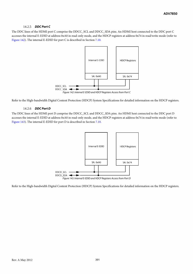
ADV7850
Rev. A May 2012 391
14.2.5 DDC Port C The DDC lines of the HDMI port C comprise the DDCC_SCL and DDCC_SDA pins. An HDMI host connected to the DDC port C accesses the internal E-EDID at address 0xA0 in read-only mode, and the HDCP registers at address 0x74 in read/write mode (refer to Figure 142). The internal E-EDID for port C is described in Section 7.10.
Figure 142: Internal E-EDID and HDCP Registers Access from Port C
Refer to the High-bandwidth Digital Content Protection (HDCP) System Specifications for detailed information on the HDCP registers.
14.2.6 DDC Port D The DDC lines of the HDMI port D comprise the DDCC_SCL and DDCC_SDA pins. An HDMI host connected to the DDC port D accesses the internal E-EDID at address 0xA0 in read-only mode, and the HDCP registers at address 0x74 in read/write mode (refer to Figure 143). The internal E-EDID for port D is described in Section 7.10.
Figure 143: Internal E-EDID and HDCP Registers Access from Port D
Refer to the High-bandwidth Digital Content Protection (HDCP) System Specifications for detailed information on the HDCP registers.

ADV7850
Rev. A May 2012 392
15 INTERRUPTS
15.1 INTERRUPT ARCHITECTURE OVERVIEW The ADV7850 has a comprehensive set of interrupt registers located in the IO Map and the HDMI Tx Map. These interrupts can be used to indicate certain events in the HDMI Rx section, the CP, the SDP, and also the HDMI Tx. The ADV7850 features several interrupt controllers that handle two separate interrupt signals. These interrupt signals are available on the interrupt pins INT0 and INT1.
15.2 INTERRUPT PINS The ADV7850 features two dedicated interrupt pins, INT1 and INT2. INT1 is always enabled, but INT2 is disabled by default and must be enabled usingint2_en, IO, Address 0x41[2] This control is used to enable INT2.
Function int2_en Description 0 Disable INT2 1 Enable INT2
15.2.1 Interrupt Duration The interrupt duration can be programmed independently for INT1 and INT2. When an interrupt event occurs, the interrupt pin INT1 or INT2 becomes active with a programmable duration as described here. intrq_dur_sel[1:0], IO, Address 0x40[7:6] This control is used to select the interrupt signal duration for the interrupt signal on INT1.
Function intrq_dur_sel[1:0] Description 00 4 Xtal periods 01 16 Xtal periods 10 64 Xtal periods 11 Active until cleared
intrq2_dur_sel[1:0], IO, Address 0x41[7:6] This control is used to select the interrupt signal duration for the interrupt signal on INT2.
Function intrq2_dur_sel[1:0] Description 00 4 Xtal periods 01 16 Xtal periods 10 64 Xtal periods 11 Active until cleared
15.2.2 Interrupt Drive Level The drive level of INT1 and INT2 can be programmed independently for INT1 and INT2 as described here.

ADV7850
Rev. A May 2012 393
intrq_op_sel[1:0], IO, Address 0x40[1:0] This control is used to configure an interrupt signal for INT1.
Function intrq_op_sel[1:0] Description 00 Open drain 01 Drive low when active 10 Drive high when active 11 Disabled
intrq2_op_sel[1:0], IO, Address 0x41[1:0] This control is used to configure an interrupt signal for INT2.
Function intrq2_op_sel[1:0] Description 00 Open drain 01 Drive low when active 10 Drive high when active 11 Disabled
15.2.3 Interrupt Manual Assertion It is possible to manually generate an interrupt on the INT1 and INT2 pins by setting mpu_stim_intrq_st. This feature is designed for debug use and not intended for use in normal operation. The appropriate mask bit must be set to generate an interrupt at the pin. mpu_stim_intrq, IO, Address 0x40[2] This control is used to set a manual interrupt. This feature should be used for test purposes only. Note that the appropriate mask bit must be set to generate an interrupt at the pin.
Function mpu_stim_intrq Description 0 Disable manual interrupt mode 1 Enable manual interrupt mode
mpu_stim_intrq_mb1, IO, Address 0x4B[7] This control is used to set the INT1 interrupt mask for the manual forced interrupt signal. When set, the manual forced interrupt triggers the INT1 interrupt and mpu_stim_intrq_st indicates the interrupt status.
Function mpu_stim_intrq_mb1 Description 0 Disable manual forced interrupt for INT1 1 Enable manual forced interrupt for INT1
mpu_stim_intrq_mb2, IO, Address 0x4A[7] This control is used to set the INT2 interrupt mask for the manual forced interrupt signal. When set, the manual forced interrupt triggers the INT2 interrupt and mpu_stim_intrq_st indicates the interrupt status.
ADV7850
Rev. A May 2012 394
Function mpu_stim_intrq_mb2 Description 0 Disable manual forced interrupt for INT2 1 Enable manual forced interrupt for INT2
15.2.4 Multiple Interrupt Events If an interrupt event occurs, and then a second interrupt event occurs before the system controller has cleared or masked the first interrupt event, the ADV7850 does not generate a second interrupt signal. The system controller should check all unmasked interrupt status bits as more than one may be active.
15.3 RX SECTION This section describes the interrupt support provided for the HDMI Rx inputs for the ADV8750. The HDMI Rx interrupts are or’ed together and can be connected to either the INT1 or the INT2 pin. The ADV7850 Rx interrupt architecture provides the following types of bits:
• Raw bits • Status bits • Interrupt mask bits • Clear bits
Raw bits are defined as being either edge-sensitive or level-sensitive. The following compares avi_info_raw and new_avi_info_raw to demonstrate the difference. avi_info_raw, IO, Address 0x60[0] (Read Only) This readback indicates the raw status of the AVI InfoFrame detected signal. This bit is set to one when an AVI InfoFrame is received and is reset to 0 if no AVI InfoFrame is received for more than seven VSyncs(on the eighth VSync leading edge following the last received AVI InfoFrame), after an HDMI packet detection reset or upon writing to AVI_PACKET_ID.
Function avi_info_raw Description 0 No AVI InfoFrame received within last seven VSyncs or since last HDMI packet detection reset 1 AVI InfoFrame received within last seven VSyncs
new_avi_info_raw, IO, Address 0x79[0] (Read Only) This readback indicates the status of the new AVI InfoFrame interrupt signal. When set to 1, it indicates that an AVI InfoFrame was received with new contents. Once set, this bit remains high until the interrupt is cleared via new_avi_info_clr.
Function new_avi_info_raw Description 0 No new AVI InfoFrame received 1 AVI InfoFrame with new content received
In the case of avi_info_raw, this bit always represents the current status of whether or not the part is receiving AVI InfoFrames. It is not a latched bit and never requires to be cleared. This is the definition of a level-sensitive raw bit. This strategy would not work in the case of new_avi_info_raw. If the new_avi_info_raw bit were to behave in the same way as avi_info_raw it would go high at the instant the new InfoFrame was received, and would go low again some clock cycles afterwards. This is because a new InfoFrame is new only for the instant it is received and, once received, it is no longer new so the event to set this bit only lasts for an instant and is then gone. Having a raw bit that is only held high for an instant is not useful. Therefore, for these types of events, the raw bit is latched, and must be cleared by the corresponding clear bit. Accordingly, the raw bit does not truly represent the current status; instead it represents the status

ADV7850
Rev. A May 2012 395
of an edge event that happened in the past. This is the definition of an edge-sensitive raw bit. All raw bits, with the exceptions of intrq_raw and intrq2_raw, have corresponding status bits. The status bits always work in the same manner whether the raw bit is edge or level-sensitive. Status bits have the following characteristics:
• Enabled by setting either or both of the corresponding interrupt mask bits • Always latched and must be cleared by the corresponding clear bit
When either of the interrupt mask bits for a given interrupt is set, if that raw bit changes state, the corresponding status bit goes high and an interrupt is generated on the INT1 or INT2 pin, depending on which interrupt mask bit was set. The status bit must be cleared using the appropriate clear bit. The status bits, interrupt mask bits and clear bits for avi_info and new_avi_info are described here for completeness. avi_info_st, IO, Address 0x61[0] (Read Only) This readback indicates the latched status of the avi_info_raw signal. This bit is only valid if enabled via the corresponding INT1 or INT2 interrupt mask bit. Once set, this bit remains high until the interrupt is cleared via avi_info_clr.
Function avi_info_st Description 0 avi_info_raw not changed state 1 avi_info_raw changed state
new_avi_info_st, IO, Address 0x7A[0] (Read Only) This readback indicates the latched status for new_avi_info_raw. This bit is only valid if enabled via the corresponding INT1 or INT2 interrupt mask bit. Once set, this bit remains high until the interrupt is cleared via new_avi_info_clr.
Function new_avi_info_st Description 0 new_avi_info_raw not changed state 1 new_avi_info_raw changed state
avi_info_clr, IO, Address 0x62[0] (Self-Clearing) This control is used to clear the avi_info_raw and avi_info_st bits. This is a self clearing bit.
Function avi_info_clr Description 0 No function 1 Clear avi_info_raw and avi_info_st
new_avi_info_clr, IO, Address 0x7B[0] (Self-Clearing) This control is used to clear the new_avi_info_raw and new_avi_info_st bits. This is a self clearing bit.
Function new_avi_info_clr Description 0 No function 1 Clear new_avi_info_raw and new_avi_info_st
avi_info_mb1, IO, Address 0x64[0] This control is used to set the INT1 interrupt mask for the AVI InfoFrame detection interrupt. When set, an AVI InfoFrame detection event causes avi_info_st to be set and an interrupt generated on INT1.
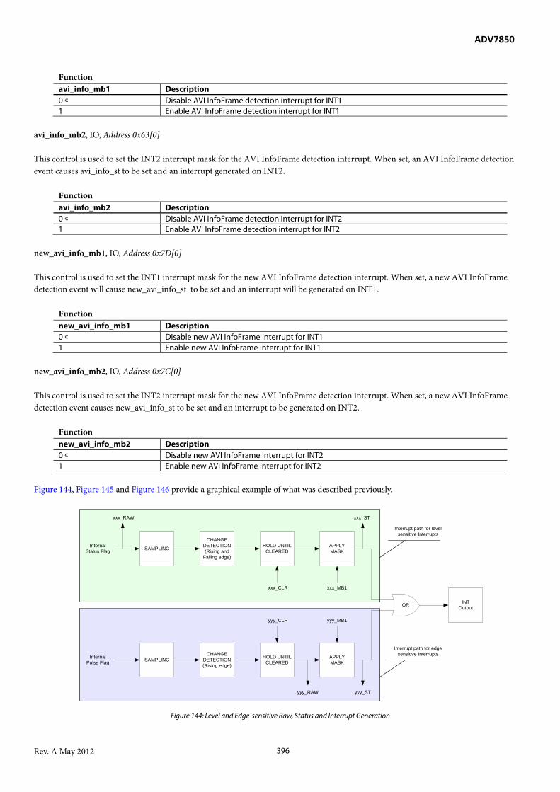
ADV7850
Rev. A May 2012 396
Function avi_info_mb1 Description 0 Disable AVI InfoFrame detection interrupt for INT1 1 Enable AVI InfoFrame detection interrupt for INT1
avi_info_mb2, IO, Address 0x63[0] This control is used to set the INT2 interrupt mask for the AVI InfoFrame detection interrupt. When set, an AVI InfoFrame detection event causes avi_info_st to be set and an interrupt generated on INT2.
Function avi_info_mb2 Description 0 Disable AVI InfoFrame detection interrupt for INT2 1 Enable AVI InfoFrame detection interrupt for INT2
new_avi_info_mb1, IO, Address 0x7D[0] This control is used to set the INT1 interrupt mask for the new AVI InfoFrame detection interrupt. When set, a new AVI InfoFrame detection event will cause new_avi_info_st to be set and an interrupt will be generated on INT1.
Function new_avi_info_mb1 Description 0 Disable new AVI InfoFrame interrupt for INT1 1 Enable new AVI InfoFrame interrupt for INT1
new_avi_info_mb2, IO, Address 0x7C[0] This control is used to set the INT2 interrupt mask for the new AVI InfoFrame detection interrupt. When set, a new AVI InfoFrame detection event causes new_avi_info_st to be set and an interrupt to be generated on INT2.
Function new_avi_info_mb2 Description 0 Disable new AVI InfoFrame interrupt for INT2 1 Enable new AVI InfoFrame interrupt for INT2
Figure 144, Figure 145 and Figure 146 provide a graphical example of what was described previously.
Figure 144: Level and Edge-sensitive Raw, Status and Interrupt Generation
SAMPLING
CHANGE DETECTION(Rising and
Falling edge)
HOLD UNTILCLEARED
APPLYMASK
OR
SAMPLINGCHANGE
DETECTION(Rising edge)
HOLD UNTILCLEARED
APPLYMASK
INTOutput
InternalStatus Flag
InternalPulse Flag
xxx_RAW xxx_ST
xxx_CLR xxx_MB1
yyy_CLR yyy_MB1
yyy_RAW yyy_ST
Interrupt path for level sensitive Interrupts
Interrupt path for edge sensitive Interrupts

ADV7850
Rev. A May 2012 397
Figure 145: AVI_INFO_RAW and AVI_INFO_ST Timing
Figure 146: NEW_AVI_INFO_RAW and NEW_AVI_INFO_ST Timing In this section, all raw bits are classified as being triggered by either level-sensitive or edge-sensitive events, with the following understanding of the terminology. Level-sensitive events are events that are generally either high or low and which are not expected to change rapidly. The raw bit for level-sensitive events is not latched and, therefore, always represents the true real-time status of the event in question. Edge-sensitive events are events that only exist for an instant. The raw bits for edge-sensitive events are latched and, therefore, represent the occurrence of an edge-sensitive event that happened in the past. Raw bits for edge-sensitive events must be cleared by the corresponding clear bit.
AVI InfoFrame Detected
No AVI InfoFrame Detected
AVI infoFrame Detection
Internal Flag
AVI_INFO_RAW
AVI_INFO_ST
AVI_INFO_CLR set to 1
AVI_INFO_CLR set to 1
Time taken by the CPU to clearAVI_INFO_ST
Time taken by the CPU to clearAVI_INFO_ST
AVI InfoFrame with new content detected
New AVI InfoFrame Detection Internal
Pulse Flag
NEW_AVI_INFO_RAW
NEW_AVI_INFO_ST
NEW_AVI_INFO_CLR set to 1
Time taken by the CPU to clear
NEW_AVI_INFO_ST
Time > 2 xtal periods

ADV7850
Rev. A May 2012 398
15.4 DESCRIPTION OF RX INTERRUPT BITS This section lists all the raw bits in the IO Map of the ADV7850 by category, and states whether the bit is an edge- or level-sensitive bit. A basic explanation for each bit is provided in the software manual and/or in the corresponding section of this manual. For certain interrupts that require additional explanations, these are provided in the subsections of this section.
15.4.1 General Operation • intrq_raw (level-sensitive event) • intrq2_raw (level-sensitive event) • afe_interrupt_raw (edge-sensitive event) • mpu_stim_intrq_raw (edge-sensitive event)
15.4.2 Analog/HDMI Video Mode • sdp_std_changed_raw (edge-sensitive event) • sdp_burst_locked_raw (level-sensitive event) • sdp_video_detected_raw (level-sensitive event) • sspd_rslt_chngd_raw (edge-sensitive event) • sspd_rslt_chngd_ch1_raw (edge-sensitive event) • sspd_rslt_chngd_ch2_raw (edge-sensitive event) • stdi_data_valid_raw (edge/level-sensitive event .. programmable) • stdi_dvalid_ch1_raw (edge/level-sensitive event .. programmable)1 • stdi_dvalid_ch2_raw (edge/level-sensitive event .. programmable)1 • cp_unlock_raw (edge/level-sensitive event .. programmable)1 • cp_unlock_ch1_raw (edge/level-sensitive event .. programmable)1 • cp_unlock_ch2_raw (edge/level-sensitive event .. programmable)1 • cp_lock_raw (edge/level-sensitive event .. programmable)1 • cp_lock_ch1_raw (edge/level-sensitive event .. programmable)1 • cp_lock_ch2_raw (edge/level-sensitive event .. programmable)1
15.4.3 Macrovision Detection The following raw bits are related to Macrovision detection and are based on level-sensitive events. Therefore, it is not necessary to clear these bits.
• mv_agc_det_raw • mv_ps_det_raw • mv_cs_det_raw
15.4.4 VDP Operation The following raw bits are related to analog video VDP operation and are based on edge-sensitive events. Therefore, it is necessary to clear these bits using the corresponding clear bit.
• cp_cgms_chngd_raw • ttxt_avl_raw • vitc_avl_raw • gs_data_type_raw • gs_pdc_vps_utc_avl_raw • cgms_wss_avl_raw • ccap_even_field_raw • ccap_avl_raw • spi_ data_rdy_raw
15.4.5 HDMI Only Mode The following raw bits are all related to HDMI operation and are based on level-sensitive events; it is therefore not necessary to clear these bits.
• isrc2_pckt_raw • isrc1_pckt_raw

ADV7850
Rev. A May 2012 399
• acp_pckt_raw • vs_info_raw • ms_info_raw • spd_info_raw • audio_info_raw • avi_info_raw • cs_data_valid_raw • internal_mute_raw • av_mute_raw • audio_ch_md_raw • hdmi_mode_raw • gen_ctl_pckt_raw • audio_c_pckt_raw • gamut_mdata_raw • tmdspll_lck_a_raw • tmdspll_lck_b_raw • tmdspll_lck_c_raw • tmdspll_lck_d_raw • tmds_clk_a_raw • tmds_clk_b_raw • tmds_clk_c_raw • tmds_clk_d_raw • hdmi_encrpt_a_raw • hdmi_encrpt_b_raw • hdmi_encrpt_c_raw • hdmi_encrpt_d_raw • cable_det_a_raw • cable_det_b_raw • cable_det_c_raw • cable_det_d_raw • v_locked_raw • de_regen_lck_raw • video_3d_raw
The following raw bits are related to HDMI operation and are based on edge-sensitive events. Therefore, it is necessary to clear these bits using the corresponding clear bit.
• new_isrc2_pckt_raw • new_isrc1_pckt_raw • new_acp_pckt_raw • new_vs_info_raw • new_ms_info_raw • new_spd_info_raw • new_audio_info_raw • new_avi_info_raw • fifo_near_ovfl_raw • fifo_underflo_raw • fifo_overflo_raw • cts_pass_thrsh_raw • change_n_raw • packet_error_raw • audio_pckt_err_raw • new_gamut_mdata_raw • deep_color_chng_raw • vclk_chng_raw

ADV7850
Rev. A May 2012 400
• audio_mode_chng_raw • parity_error_raw • new_samp_rt_raw • audio_flt_line_raw • new_tmds_frq_raw • fifo_near_uflo_raw • ms_inf_cks_err_raw • spd_inf_cks_err_raw • aud_inf_cks_err_raw • avi_inf_cks_err_raw • aksv_update_a_raw • aksv_update_b_raw • aksv_update_c_raw • aksv_update_d_raw • bg_meas_done_raw • vs_inf_cks_err_raw • ri_expired_a_raw • ri_expired_b_raw • ri_expired_c_raw • ri_expired_d_raw
15.5 ADDITIONAL EXPLANATIONS
15.5.1 afe_interrupt_raw The AFE section contains the logic to slice eight trilevel inputs. Each trilevel input has two independently programmable slice levels, and an interrupt associated with each slice level. Therefore, the AFE section can generate 16 different interrupts related to the eight trilevel inputs. afe_interrupt_raw Each trilevel input has an interrupt mask control (trix_int_mask[1:0] where X = 1 to 8) which enables or disables interrupt generation when a trilevel input crosses its upper or lower slice level, a read-only status value (trix_int_status[1:0]) to indicate which trilevel input has generated an interrupt, and an interrupt clear control (trix_int_clear[1:0]) to clear latched interrupts. Real-time trilevel status can be obtained by reading trix_readback[1:0]. The 16 possible AFE interrupts are or’ed together and used to trigger the IO Map afe_interrupt_raw bit. For example, to generate an interrupt on INT2 when trilevel 6 crosses its upper slice level, firstly, tri6_int_mask[1:0] in the AFE Map must be set to 0b10 to generate an interrupt when trilevel 6 input crosses its upper slice level, secondly, afe_interrupt_mb2 in the IO Map must be set to 0b1 to generate an interrupt on INT2 when afe_interrupt_raw is set. The flowchart in Figure 147 suggests a method to handle the afe_interrupt interrupt to avoid missing any interrupts that occur at the same time, or while servicing another interrupt.

ADV7850
Rev. A May 2012 401
Figure 147: Suggested Method of Handling afe_interrupt
TRIX_INT_STATUS[1:0]=0b00 ?
START(AFE_INTERRUPT received)
Y
Y
Set variable “X” = 1
Read TRIX_INT_STATUS[1:0]
No interrupt on TRIX
Increment variable “X”
X = 9 ?
All tri-level input status readbacks checked
N
Interrupt on TRIX
Read TRIX_READBACK[1:0]to determine current status of
TRIX input and performappropriate action
N
Clear AFE_INTERRUPT_ST in IO map
Check AFE_INTERRUPT_RAW in IO map
AFE_INTERRUPT_RAW=0b0 ?
END
N
Y

ADV7850
Rev. A May 2012 402
15.5.2 stdi_data_valid_raw stdi_data_valid_raw is programmable as either an edge-sensitive bit or a level-sensitive bit using stdi_data_valid_edge_sel. Note that this control also configures whether an interrupt is generated only on the rising edge of stdi_data_valid_raw, or on both edges. stdi_data_valid_edge_sel, IO, Address 0x41[4] This control is used to configure the functionality of the stdi_data_valid interrupt. The interrupt can be generated when STDI changes to an STDI valid state. Alternatively, it can be generated to indicate a change in stdi_valid status.
Function stdi_data_valid_edge_sel
Description
0 Generate interrupt for a low to high change in stdi_valid status 1 Generate interrupt for a low to high or a high to low change in stdi_valid status
15.5.3 cp_lock, cp_unlock cp_unlock_raw is programmable as either an edge-sensitive bit or a level-sensitive bit using cp_lock_unlock_edge_sel. Note that this control also configures whether an interrupt is generated only on the rising edge of cp_unlock_raw or on both edges. cp_lock_unlock_edge_sel, IO, Address 0x41[5] This control is used to configure the functionality of the cp_lock and unlock interrupts.
Function cp_lock_unlock_edge_sel
Description
0 Generate interrupt for a low to high change in cp_lock and unlock status for channel 1 and channel 2
1 Generate interrupt for a low to high or a high to low change in cp_lock and unlock status for channel 1 and channel 2
cp_unlock_st, IO, Address 0x43[3] (Read Only) This readback indicates the latched signal status of the CP unlock interrupt signal. Once set, this bit remains high until the interrupt is cleared via cp_unlock_clr. This bit is only valid if enabled via the corresponding INT1 or INT2 interrupt mask bit.
Function cp_unlock_st Description 0 No CP unlock interrupt event occurred 1 CP unlock interrupt event occurred
cp_lock_st, IO, Address 0x43[2] (Read Only) This readback indicates the latched signal status of the CP lock interrupt signal. Once set, this bit remains high until the interrupt is cleared via cp_lock_clr. This bit is only valid if enabled via the corresponding INT1 or INT2 interrupt mask bit.
Function cp_lock_st Description 0 No CP LOCK interrupt event occurred 1 CP LOCK interrupt event occurred

ADV7850
Rev. A May 2012 403
15.5.4 Video 3D Detection The ADV7850 allows checking for 3D HDMI activity using the following controls. video_3d_raw, IO, Address 0x74[2] (Read Only) This readback indicates the raw status of the Video 3D signal.
Function video_3d_raw Description 0 Video 3D not detected 1 Video 3D detected
15.5.5 HDMI Interrupts Validity Checking Process All HDMI interrupts have a set of conditions that must be taken into account for validation in the display firmware. When the ADV7850 interrupts the display controller for an HDMI interrupt, the host must check that all validity conditions for that interrupt are met before processing that interrupt. For simplicity, HDMI interrupts can be subdivided into three groups, as described in Section 15.5.5.1, Section 15.5.5.2 and Section 15.5.5.3.
15.5.5.1 Group 1 HDMI Interrupts The interrupts listed in Table 105 are valid irrespective of the mode in which the ADV7850 is configured, that is:
• COMP mode (prim_mode set to 0x01) • GR mode (prim_mode set to 0x02) • HDMI mode (prim_mode set to values 0x05 or 0x06)
Table 105: HDMI Interrupts Group 1
Interrupts tmds_clk_a tmds_clk_b tmds_clk_c tmds_clk_d cable_det_a cable_det_b cable_det_c cable_det_d
15.5.5.2 Group 2 HDMI Interrupts The interrupts listed in Table 106 are valid on the condition that the ADV7850 is configured in HMDI mode.
Table 106: HDMI Interrupts Group 2 Interrupts internal_mute video_pll_lck aksv_update v_locked de_regen_lck
15.5.5.3 Group 3 HDMI Interrupts The interrupts listed in Table 107 are valid under the following conditions:
• ADV7850 is configured in HMDI mode • TMDS_CLK_A_RAW is set to 1 if port A is the active HDMI port • TMDS_CLK_B_RAW is set to 1 if port B is the active HDMI port • TMDS_CLK_C_RAW is set to 1 if port C is the active HDMI port • TMDS_CLK_D_RAW is set to 1 if port D is the active HDMI port

ADV7850
Rev. A May 2012 404
• VIDEO_PLL_LOCKED_RAW is set to 1
Table 107: HDMI Interrupts Group 3 Interrupts isrc2_pckt isrc1_pckt acp_pckt vs_info ms_info
spd_info audio_info avi_info cs_data_valid av_mute audio_ch_md audio_mode_change gen_ctl_pckt audio_c_pckt gamut_mdata hdmi_mode hdmi_encrpt new_isrc2_info new_isrc1_info new_acp_info new_vs_info new_ms_info new_spd_info new_audio_info new_avi_info fifo_near_ovfl cts_pass_thrsh change_n packet_error audio_pckt_err new_gamut_data deep_color_chng vclk_chng parrity_error new_samp_rt audio_flt_line new_tmds_frq fifo_near_uflo
15.5.6 Storing Masked Interrupts store_unmasked_irqs, IO, Address 0x40[4] This control is used to allow the HDMI status flags for any HDMI interrupt to be triggered regardless of whether or not the mask bits are set. This bit allows an HDMI interrupt to trigger and allows this interrupt to be read back through the corresponding status bit without triggering an interrupt on the interrupt pin. The status is stored until the clear bit is used to clear the status register and allows another interrupt to occur.
Function store_unmasked_irqs Description 0 Do not allow x_ST flag of any HDMI interrupt to be set independently of mask bits 1 Allow x_ST flag of any HDMI interrupt to be set independently of mask bits
15.5.6.1 Interrupt Status Registers The Trilevel Interrupt Status 1 register consists of the following fields.

ADV7850
Rev. A May 2012 405
tri1_int_status[1:0], AFE, Address 0x1B[7:6] (Read Only) This readback displays the Tri1 interrupt status.
Function tri1_int_status[1:0] Description 00 No signal change detected 01 Signal crossed lower slice level 10 Signal crossed upper slice level 11 Signal crossed both slice levels
tri2_int_status[1:0], AFE, Address 0x1B[5:4] (Read Only) This readback displays the Tri2 interrupt status.
Function tri2_int_status[1:0] Description 00 No signal change detected 01 Signal crossed lower slice level 10 Signal crossed upper slice level 11 Signal crossed both slice levels
tri3_int_status[1:0], AFE, Address 0x1B[3:2] (Read Only) This readback displays the Tri3 interrupt status.
Function tri3_int_status[1:0] Description 00 No signal change detected 01 Signal crossed lower slice level 10 Signal crossed upper slice level 11 Signal crossed both slice levels
tri4_int_status[1:0], AFE, Address 0x1B[1:0] (Read Only) This readback displays the Tri4 interrupt status.
Function tri4_int_status[1:0] Description 00 No signal change detected 01 Signal crossed lower slice level 10 Signal crossed upper slice level 11 Signal crossed both slice levels
The Trilevel Interrupt Status 2 register consists of the following fields. tri5_int_status[1:0], AFE, Address 0x1C[7:6] (Read Only) This readback displays the Tri5 interrupt status.
Function tri5_int_status[1:0] Description 00 No signal change detected 01 Signal crossed lower slice level 10 Signal crossed upper slice level 11 Signal crossed both slice levels

ADV7850
Rev. A May 2012 406
tri6_int_status[1:0], AFE, Address 0x1C[5:4] (Read Only) This readback displays the Tri6 interrupt status.
Function tri6_int_status[1:0] Description 00 No signal change detected 01 Signal crossed lower slice level 10 Signal crossed upper slice level 11 Signal crossed both slice levels
tri7_int_status[1:0], AFE, Address 0x1C[3:2] (Read Only) This readback displays the Tri7 interrupt status.
Function tri7_int_status[1:0] Description 00 No signal change detected 01 Signal crossed lower slice level 10 Signal crossed upper slice level 11 Signal crossed both slice levels
tri8_int_status[1:0], AFE, Address 0x1C[1:0] (Read Only) This readback displays the Tri8 interrupt status.
Function tri8_int_status[1:0] Description 00 No signal change detected 01 Signal crossed lower slice level 10 Signal crossed upper slice level 11 Signal crossed both slice levels
The interrupt_status_1 register consists of the following fields. sspd_rslt_chngd_st, IO, Address 0x43[7] (Read Only) This readback indicates the latched signal status of the SSPD result changed interrupt signal. Once set, this bit remains high until the interrupt is cleared via sspd_rslt_chngd_clr. This bit is only valid if enabled via the corresponding INT1 or INT2 interrupt mask bit.
Function sspd_rslt_chngd_st Description 0 No SSPD result changed interrupt event occurred 1 SSPD result changed interrupt event occurred
mv_ps_det_st, IO, Address 0x43[6] (Read Only) This readback indicates the latched signal status of the Macrovision pseudo sync detected interrupt signal. Once set, this bit remains high until the interrupt is cleared via mv_ps_det_clr. This bit is only valid if enabled via the corresponding INT1 or INT2 Interrupt mask bit.

ADV7850
Rev. A May 2012 407
Function mv_ps_det_st Description 0 No Macrovision pseudo sync detection interrupt event occurred 1 Macrovision pseudo sync detected interrupt event occurred
stdi_data_valid_st, IO, Address 0x43[4] (Read Only) This readback indicates the latched signal status of the STDI valid interrupt signal. Once set, this bit remains high until the interrupt is cleared via stdi_data_valid_clr. This bit is only valid if enabled via the corresponding INT1 or INT2 interrupt mask bit.
Function stdi_data_valid_st Description 0 No STDI valid interrupt occurred 1 STDI valid interrupt occurred
afe_interrupt_st, IO, Address 0x43[0] (Read Only) This readback indicates the latched signal status of the AFE interrupt signal. Once set, this bit remains high until the interrupt is cleared via afe_interrupt_clr. This bit is only valid if enabled via the corresponding INT1 or INT2 interrupt mask bit.
Function afe_interrupt_st Description 0 No AFE interrupt event occurred 1 AFE interrupt event occurred
The interrupt_status_2 register consists of the following fields. mpu_stim_intrq_st, IO, Address 0x48[7] (Read Only) This readback indicates the latched signal status of the forced manual interrupt signal. Once set, this bit remains high until the interrupt is cleared via mpu_stim_intrq_clr. This bit is only valid if enabled via the corresponding INT1 or INT2 interrupt mask bit.
Function mpu_stim_intrq_st Description 0 Forced manual interrupt event not occurred 1 Forced manual interrupt event occurred
mv_agc_det_st, IO, Address 0x48[6] (Read Only) This readback indicates the latched signal status of the Macrovision AGC detected interrupt signal. Once set, this bit remains high until the interrupt is cleared via mv_agc_det_clr. This bit is only valid if enabled via the corresponding INT1 or INT2 interrupt mask bit.
Function mv_agc_det_st Description 0 Macrovision AGC detected interrupt event not occurred 1 Macrovision AGC detected interrupt event occurred
mv_cs_det_st, IO, Address 0x48[5] (Read Only) This readback indicates the latched signal status of the Macrovision color stripe detected interrupt signal. Once set, this bit remains high until the interrupt is cleared via mv_cs_det_clr. This bit is only valid if enabled via the corresponding INT1 or INT2 mask bit.
ADV7850
Rev. A May 2012 408
Function mv_cs_det_st Description 0 Macrovision color stripe detected interrupt event not occurred 1 Macrovision color stripe detected interrupt event occurred
cp_cgms_chngd_st, IO, Address 0x48[2] (Read Only) This readback indicates the latched signal status of the CP CGMS changed interrupt signal. Once set, this bit remains high until the interrupt is cleared via cp_cgms_chngd_clr. This bit is only valid if enabled via the corresponding INT1 or INT2 interrupt mask bit.
Function cp_cgms_chngd_st Description 0 CGMS data changed, interrupt event occurred 1 CGMS data changed, interrupt event occurred
The interrupt_status_3 register consists of the following fields. avlink_rx_ready_st, Addr 40 (IO), Address 0x4D[3] (Read Only) Latched status of AV.link Receiver ready interrupt signal. Once set this bit will remain high until the interrupt has been cleared via avlink_rx_ready_clr. This bit is only valid if enabled via the corresponding INT1 or INT2 interrupt mask bit.
Function avlink_rx_ready_st Description 0 << AV.link message received interrupt has not occurred. 1 AV.link message received interrupt has occurred.
avlink_tx_ready_st, Addr 40 (IO), Address 0x4D[0] (Read Only) Latched status of avlink_tx_ready_raw signal. This bit is only valid if enabled via the corresponding INT1 or INT2 interrupt mask bit. When the AV.link TX successfully sends the current message this bit is set. Once set this bit will remain high until the interrupt has been cleared via avlink_tx_ready_clr.
Function avlink_tx_ready_st Description 0 << No change 1 Message transmitted successfully
The interrupt_status_4 register consists of the following fields. ttxt_avl_st, IO, Address 0x52[7] (Read Only) This readback indicates the latched status of theteletext data available interrupt signal. Once set, this bit remains high until the interrupt is cleared via ttxt_avl_clr. This bit is only valid if enabled via the corresponding INT1 or INT2 interrupt mask bit.
Function ttxt_avl_st Description 0 No teletext data available, no interrupt 1 Teletext data available, interrupt event occurred
vitc_avl_st, IO, Address 0x52[6] (Read Only) This readback indicates the latched status of the VITC data available interrupt signal. Once set, this bit remains high until the interrupt is cleared via vitc_avl_clr. This bit is only valid if enabled via the corresponding INT1 or INT2 interrupt mask bit.

ADV7850
Rev. A May 2012 409
Function vitc_avl_st Description 0 No VITC data available interrupt event occurred 1 VITC data available interrupt event occurred
gs_data_type_st, IO, Address 0x52[5] (Read Only) This readback indicates the latched status of the Gemstar type available interrupt signal. Once set, this bit remains high until the interrupt is cleared via gs_data_type_clr. This bit is only valid if enabled via the corresponding INT1 or INT2 interrupt bit.
Function gs_data_type_st Description 0 No Gemstar data type interrupt event occurred 1 Gemstar data type interrupt event occurred
gs_pdc_vps_utc_avl_st, IO, Address 0x52[4] (Read Only) This readback indicates the latched status of the Gemstar/PDC/VPS/UTC data available interrupt signal. Once set, this bit remains high until the interrupt is cleared via gs_pdc_vps_utc_avl_clr. This bit is only valid if enabled via corresponding the INT1 or INT2 interrupt mask bit.
Function gs_pdc_vps_utc_avl_st Description 0 No Gemstar/PDC/VPS/UTC data available interrupt event occurred 1 Gemstar/PDC/VPS/UTC data available interrupt event occurred
cgms_wss_avl_st, IO, Address 0x52[2] (Read Only) This readback indicates the latched status of the CGMS/WSS data available interrupt signal. Once set, this bit remains high until the interrupt is cleared via cgms_wss_avl_clr. This bit is only valid if enabled via the corresponding INT1 or INT2 interrupt bit.
Function cgms_wss_avl_st Description 0 No CGMS/WSS data available interrupt event occurred 1 CGMS/WSS data available interrupt event occurred
ccap_even_field_st, IO, Address 0x52[1] (Read Only) This readback indicates the latched status of the closed captioning detected on even field interrupt signal. Once set, this bit remains high until the interrupt is cleared via ccap_even_field_clr. This bit is only valid if enabled via the corresponding INT1 or INT2 interrupt mask bit.
Function ccap_even_field_st Description 0 No closed captioning detected on even field interrupt event occurred 1 Closed captioning detected on even field interrupt event occurred
ccap_avl_st, IO, Address 0x52[0] (Read Only) This readback indicates the latched status of the closed captioning data available interrupt signal. Once set, this bit remains high until the interrupt is cleared via ccap_avl_clr. This bit is only valid if enabled via the corresponding INT1 or INT2 interrupt mask bit.

ADV7850
Rev. A May 2012 410
Function ccap_avl_st Description 0 No closed captioning data available interrupt event occurred 1 Closed captioning data available interrupt event occurred
The interrupt_status_5 register consists of the following fields. sdp_progressive_st, Addr 40 (IO), Address 0x57[7] (Read Only)
Function sdp_progressive_st Description 0 << No change. An interrupt has not been generated from this register. 1 esdp_progressive_raw has changed and generated an interrupt.
sdp_pr_det_st, Addr 40 (IO), Address 0x57[6] (Read Only)
Function sdp_pr_det_st Description 0 << No change. An interrupt has not been generated from this register. 1 esdp_pr_det_raw has changed and generated an interrupt.
sdp_sd_det_st, Addr 40 (IO), Address 0x57[5] (Read Only)
Function sdp_sd_det_st Description 0 << No change. An interrupt has not been generated from this register. 1 esdp_sd_det_raw has changed and generated an interrupt.
sdp_50hz_det_st, Addr 40 (IO), Address 0x57[4] (Read Only)
Function sdp_50hz_det_st Description 0 << No change. An interrupt has not been generated from this register. 1 esdp_50hz_det_raw has changed and generated an interrupt.
The interrupt_status_6 register consists of the following fields. cp_lock_ch2_st, IO, Address 0x5C[7] (Read Only) This readback indicates that STDI channel 2 has changed from an unlocked state to a locked state.
Function cp_lock_ch2_st Description 0 No change, no interrupt generated 1 Channel 2 CP input caused the decoder to go from unlocked to locked state
cp_unlock_ch2_st, IO, Address 0x5C[6] (Read Only) This readback indicates that STDI channel 2 has changed from a locked state to an unlocked state.
Function cp_unlock_ch2_st Description 0 No change, no interrupt generated 1 CP input caused the decoder to go from locked to unlocked state
stdi_dvalid_ch2_st, IO, Address 0x5C[5] (Read Only) This readback indicates the latched signal status of the STDI valid for sync channel 2 interrupt signal. Once set, this bit remains high until the interrupt is cleared via stdi_data_valid_ch2_clr. This bit is only valid if enabled via the corresponding INT1 or INT2 interrupt mask bit.

ADV7850
Rev. A May 2012 411
Function stdi_dvalid_ch2_st Description 0 No STDI valid for sync channel 2 interrupt occurred 1 STDI valid for sync channel 2 interrupt occurred
cp_lock_ch1_st, IO, Address 0x5C[3] (Read Only) This readback indicates that STDI channel 1 has changed from an unlocked state to a locked state.
Function cp_lock_ch1_st Description 0 No change. No interrupt generated . 1 Channel 1 CP input caused decoder to go from unlocked to locked state.
cp_unlock_ch1_st, IO, Address 0x5C[2] (Read Only) This readback indicates that STDI channel 1 has changed from a locked state to an unlocked state.
Function cp_unlock_ch1_st Description 0 No change. No interrupt generated . 1 Channel 1 CP input changed from locked to unlocked state and triggered an interrupt
stdi_dvalid_ch1_st, IO, Address 0x5C[1] (Read Only) This readback indicates the latched signal status of the STDI valid for sync channel 1 interrupt signal. Once set, this bit remains high until the interrupt is cleared via stdi_data_valid_ch1_clr. This bit is only valid if enabled via the corresponding INT1 or INT2 interrupt mask bit.
Function stdi_dvalid_ch1_st Description 0 No STDI valid for sync channel 1 interrupt occurred 1 STDI valid for sync channel 1 interrupt occurred
sspd_rslt_chngd_ch1_st The HDMI Lvl INT Status 1 register consists of the following fields. isrc2_pckt_st, IO, Address 0x61[7] (Read Only) This readback indicates the latched status of the ISRC2 packet detected interrupt signal. Once set, this bit remains high until the interrupt is cleared via isrc2_info_clr. This bit is only valid if enabled via the corresponding INT1 or INT2 interrupt mask bit.
Function isrc2_pckt_st Description 0 No interrupt generated 1 isrc2_pckt_raw changed, interrupt generated
isrc1_pckt_st, IO, Address 0x61[6] (Read Only) This readback indicates the latched status of ISRC1 packet detected interrupt signal. Once set, this bit remains high until the interrupt is cleared via isrc1_info_clr. This bit is only valid if enabled via the corresponding INT1 or INT2 interrupt mask bit.

ADV7850
Rev. A May 2012 412
Function isrc1_pckt_st Description 0 No interrupt generated 1 isrc1_packet_raw changed, interrupt generated
acp_pckt_st, IO, Address 0x61[5] (Read Only) This readback indicates the latched status of the audio content protection packet detected interrupt signal. Once set, this bit remains high until the interrupt is cleared via acp_info_clr. This bit is only valid if enabled via the corresponding INT1 or INT2 mask bit.
Function acp_pckt_st Description 0 No interrupt generated 1 acp_pckt_raw changed, interrupt generated
vs_info_st, IO, Address 0x61[4] (Read Only) This readback indicates the latched status of the vendor specific InfoFrame detected interrupt signal. Once set, this bit remains high until the interrupt is cleared via vs_info_clr. This bit is only valid if enabled via the corresponding INT1 or INT2 interrupt mask bit.
Function vs_info_st Description 0 No interrupt generated 1 vs_info_raw changed, interrupt generated
ms_info_st, IO, Address 0x61[3] (Read Only) This readback indicates the latched status of the MPEG source InfoFrame detected interrupt signal. Once set, this bit remains high until the interrupt is cleared via ms_info_clr. This bit is only valid if enabled via the corresponding INT1 or INT2 interrupt mask bit.
Function ms_info_st Description 0 No interrupt generated 1 ms_info_raw changed, interrupt generated
spd_info_st, IO, Address 0x61[2] (Read Only) This readback indicates the latched status of the SPD InfoFrame detected interrupt signal. Once set, this bit remains high until the interrupt is cleared via spd_info_clr. This bit is only valid if enabled via the corresponding INT1 or INT2 interrupt mask bit.
Function spd_info_st Description 0 No interrupt generated 1 spd_info_raw changed, interrupt generated
audio_info_st, IO, Address 0x61[1] (Read Only) This readback indicates the latched status of the audio InfoFrame detected interrupt signal. Once set, this bit remains high until the interrupt is cleared via audio_info_clr. This bit is only valid if enabled via the corresponding INT1 or INT2 interrupt mask bit.
Function audio_info_st Description 0 No interrupt generated 1 audio_inf_raw changed, interrupt generated

ADV7850
Rev. A May 2012 413
The HDMI Lvl INT Status 2 register consists of the following fields. cs_data_valid_st, IO, Address 0x66[7] (Read Only) This readback indicates the latched status of the channel status data valid interrupt signal. Once set, this bit remains high until the interrupt is cleared via cs_data_valid_clr. This bit is only valid if enabled via the corresponding INT1 or INT2 interrupt mask bit.
Function cs_data_valid_st Description 0 cs_data_valid_raw not changed, interrupt not generated 1 cs_data_valid_raw changed, interrupt generated
internal_mute_st, IO, Address 0x66[6] (Read Only) This readback indicates the latched status of Internal Mute interrupt signal. Once set, this bit remains high until the interrupt is cleared via internal_mute_clr. This bit is only valid if enabled via the corresponding INT1 or INT2 interrupt mask bit
Function internal_mute_st Description 0 internal_mute_raw not changed, interrupt not generated 1 internal_mute_raw changed, interrupt generated
av_mute_st, IO, Address 0x66[5] (Read Only) This readback indicates the latched status of the AV mute detected interrupt signal. Once set, this bit remains high until the interrupt is cleared via av_mute_clr. This bit is only valid if enabled via the corresponding INT1 or INT2 interrupt mask bit.
Function av_mute_st Description 0 av_mute_raw not changed, interrupt not generated 1 av_mute_raw changed, interrupt generated
audio_ch_md_st, IO, Address 0x66[4] (Read Only) This readback indicates the latched status of the audio channel mode interrupt signal. Once set, this bit remains high until the interrupt is cleared via audio_ch_md_clr. This bit is only valid if enabled via the corresponding INT1 or INT2 interrupt mask bit.
Function audio_ch_md_st Description 0 audio_ch_md_raw not changed, interrupt not generated 1 audio_....._raw changed, interrupt generated
hdmi_mode_st, IO, Address 0x66[3] (Read Only) This readback indicates the latched status of the HDMI mode interrupt signal. Once set, this bit remains high until the interrupt is cleared via hdmi_mode_clr. This bit is only valid if enabled via the corresponding INT1 or INT2 interrupt mask bit.
Function hdmi_mode_st Description 0 hdmi_mode_raw unchanged, interrupt not generated 1 (No Suggestions) changed, interrupt generated

ADV7850
Rev. A May 2012 414
gen_ctl_pckt_st, IO, Address 0x66[2] (Read Only) This readback indicates the latched status of the general control packet interrupt signal. Once set, this bit remains high until the interrupt is cleared via gen_ctl_pckt_clr. This bit is only valid if enabled via the corresponding INT1 or INT2 interrupt mask bit.
Function gen_ctl_pckt_st Description 0 gen_ctl_pckt_raw unchanged, interrupt not generated 1 gen_ctl_pckt_raw changed, interrupt generated
audio_c_pckt_st, IO, Address 0x66[1] (Read Only) This readback indicates the latched status of the audio clock regeneration packet interrupt signal. Once set, this bit remains high until the interrupt is cleared via audio_pckt_clr. This bit is only valid if enabled via the corresponding INT1 or INT2 interrupt mask bit.
Function audio_c_pckt_st Description 0 audio_c_pckt_raw unchanged, no interrupt generated 1 audio_c_pckt_raw changed, interrupt generated .
gamut_mdata_st, IO, Address 0x66[0] (Read Only) This readback indicates the latched status of the gamut metadata packet detected interrupt signal. Once set, this bit remains high until the interrupt is cleared via gamut_mdata_pckt_clr. This bit is only valid if enabled via the corresponding INT1 or INT2 mask bit.
Function gamut_mdata_st Description 0 gamut_mdata_raw unchanged, no interrupt generated 1 gamut_mdata_raw changed, interrupt generated
The HDMI Lvl INT Status 3 register consists of the following fields. tmdspll_lck_a_st, IO, Address 0x6B[7] (Read Only) This readback indicates the latched status of the Port A TMDS PLL lock interrupt signal. Once set, this bit remains high until the interrupt is cleared via tmdspll_lck_a_clr. This bit is only valid if enabled via the corresponding INT1 or INT2 interrupt mask bit.
Function tmdspll_lck_a_st Description 0 tmdspll_lck_a_raw not changed, interrupt not generated 1 tmdspll_lck_a_raw changed, interrupt generated
tmdspll_lck_b_st, IO, Address 0x6B[6] (Read Only) This readback indicates the latched status of the Port B TMDS PLL lock interrupt signal. Once set, this bit remains high until the interrupt is cleared via tmdspll_lck_b_clr. This bit is only valid if enabled via the corresponding INT1 or INT2 interrupt mask bit.
Function tmdspll_lck_b_st Description 0 tmdspll_lck_b_raw not changed, interrupt not generated 1 tmdspll_lck_b_raw changed, interrupt generated

ADV7850
Rev. A May 2012 415
tmdspll_lck_c_st, IO, Address 0x6B[5] (Read Only) This readback indicates the latched status of the Port C TMDS PLL lock interrupt signal. Once set, this bit remains high until the interrupt is cleared via tmdspll_lck_c_clr. This bit is only valid if enabled via the corresponding INT1 or INT2 interrupt mask bit.
Function tmdspll_lck_c_st Description 0 tmdspll_lck_c_raw not changed, interrupt not generated 1 tmdspll_lck_c_raw changed, interrupt generated
tmdspll_lck_d_st, IO, Address 0x6B[4] (Read Only) This readback indicates the latched status of the Port D TMDS PLL lock interrupt signal. Once set, this bit remains high until the interrupt is cleared via tmdspll_lck_d_clr. This bit is only valid if enabled via the corresponding INT1 or INT2 interrupt mask bit.
Function tmdspll_lck_d_st Description 0 tmdspll_lck_d_raw not changed, interrupt not generated 1 tmdspll_lck_d_raw changed, interrupt generated
tmds_clk_a_st, IO, Address 0x6B[3] (Read Only) This readback indicates the latched status of the Port A TMDS clock detection interrupt signal. Once set, this bit remains high until the interrupt is cleared via tmds_clk_a_clr. This bit is only valid if enabled via the corresponding INT1 or INT2 interrupt mask bit.
Function tmds_clk_a_st Description 0 tmds_clk_a_raw not changed, interrupt not generated 1 tmds_clk_a_raw changed, interrupt generated
tmds_clk_b_st, IO, Address 0x6B[2] (Read Only) This readback indicates the latched status of the Port B TMDS clock detection interrupt signal .Once set, this bit remains high until the interrupt is cleared via tmds_clk_b_clr. This bit is only valid if enabled via the corresponding INT1 or INT2 interrupt mask bit.
Function tmds_clk_b_st Description 0 tmds_clk_b_raw not changed, interrupt not generated 1 tmds_clk_b_raw changed, interrupt generated
tmds_clk_c_st, IO, Address 0x6B[1] (Read Only) This readback indicates the latched status of the Port C TMDS clock detection interrupt signal. Once set, this bit remains high until the interrupt is cleared via tmds_clk_c_clr. This bit is only valid if enabled via the corresponding INT1 or INT2 interrupt mask bit.
Function tmds_clk_c_st Description 0 tmds_clk_c_raw not changed, interrupt not generated 1 tmds_clk_c_raw changed, interrupt generated
tmds_clk_d_st, IO, Address 0x6B[0] (Read Only) This readback indicates the latched status of the Port D TMDS clock detection interrupt signal. Once set, this bit remains high until the interrupt is cleared via tmds_clk_d_clr. This bit is only valid if enabled via the corresponding INT1 or INT2 interrupt mask bit.

ADV7850
Rev. A May 2012 416
Function tmds_clk_d_st Description 0 tmds_clk_d_raw not changed, interrupt not generated 1 tmds_clk_d_raw changed, interrupt generated
The HDMI Lvl INT Status 4 register consists of the following fields. hdmi_encrpt_a_st, IO, Address 0x70[7] (Read Only) This readback indicates the latched status of the Port A encryption detection interrupt signal. Once set, this bit remains high until the interrupt is cleared via hdmi_encrpt_a_clr. This bit is only valid if enabled via the corresponding INT1 or INT2 interrupt mask bit.
Function hdmi_encrpt_a_st Description 0 hdmi_encrpt_a_raw not changed, interrupt not generated 1 hdmi_encrpt_a_raw changed, interrupt generated
hdmi_encrpt_b_st, IO, Address 0x70[6] (Read Only) This readback indicates the latched status of the Port B encryption detection interrupt signal. Once set, this bit remains high until the interrupt is cleared via hdmi_encrpt_b_clr. This bit is only valid if enabled via the corresponding INT1 or INT2 interrupt mask bit.
Function hdmi_encrpt_b_st Description 0 hdmi_encrpt_b_raw not changed, interrupt not generated 1 hdmi_encrpt_b_raw changed, interrupt generated
hdmi_encrpt_c_st, IO, Address 0x70[5] (Read Only) This readback indicates the latched status of the Port C encryption detection interrupt signal. Once set, this bit remains high until the interrupt is cleared via hdmi_encrpt_c_clr. This bit is only valid if enabled via the corresponding INT1 or INT2 interrupt mask bit.
Function hdmi_encrpt_c_st Description 0 hdmi_encrpt_c_raw not changed, interrupt not generated 1 hdmi_encrpt_c_raw changed, interrupt generated
hdmi_encrpt_d_st, IO, Address 0x70[4] (Read Only) This readback indicates the latched status of the Port D encryption detection interrupt signal. Once set, this bit remains high until the interrupt is cleared via hdmi_encrpt_d_clr. This bit is only valid if enabled via the corresponding INT1 or INT2 interrupt mask bit.
Function hdmi_encrpt_d_st Description 0 hdmi_encrpt_d_raw not changed, interrupt not generated 1 hdmi_encrpt_d_raw changed, interrupt generated
cable_det_a_st, IO, Address 0x70[3] (Read Only) This readback indicates the latched status for the Port A +5 V cable detection interrupt signal. Once set, this bit remains high until the interrupt is cleared via cable_det_a_clr. This bit is only valid if enabled via the corresponding INT1 or INT2 interrupt mask bit.

ADV7850
Rev. A May 2012 417
Function cable_det_a_st Description 0 cable_det_a_raw not changed, interrupt not generated 1 cable_det_a_raw changed, interrupt generated .
cable_det_b_st, IO, Address 0x70[2] (Read Only) This readback indicates the latched status for the Port B +5 V cable detection interrupt signal. Once set, this bit remains high until the interrupt is cleared via cable_det_b_clr. This bit is only valid if enabled via the corresponding INT1 or INT2 interrupt mask bit.
Function cable_det_b_st Description 0 cable_det_b_raw not changed, interrupt not generated 1 cable_det_b_raw changed, interrupt generated
cable_det_c_st, IO, Address 0x70[1] (Read Only) This readback indicates the latched status of the Port C +5 V cable detection interrupt signal. Once set, this bit remains high until the interrupt is cleared via cable_det_c_clr. This bit is only valid if enabled via the corresponding INT1 or INT2 interrupt mask bit.
Function cable_det_c_st Description 0 cable_det_c_raw not changed, interrupt not generated 1 cable_det_c_raw changed, interrupt generated
cable_det_d_st, IO, Address 0x70[0] (Read Only) This readback indicates the latched status of the Port D +5 V cable detection interrupt signal. When set, the Port D +5 V cable detection interrupt triggers the INT2 interrupt and cable_det_d_st indicates the interrupt status.
Function cable_det_d_st Description 0 cable_det_d_raw not changed, interrupt not generated 1 cable_det_d_raw changed, interrupt generated
The HDMI Lvl INT Status 5 register consists of the following fields. video_3d_st, IO, Address 0x75[2] (Read Only) This readback indicates the latched status for the Video 3D interrupt. Once set, this bit remains high until the interrupt is cleared via video_3d_clr. This bit is only valid if enabled via the corresponding INT1 or INT2 interrupt mask bit.
Function video_3d_st Description 0 video_3d_raw not changed, interrupt not generated 1 video_3d_raw changed, interrupt generated
v_locked_st, IO, Address 0x75[1] (Read Only) This readback indicates the latched status of the vertical sync filter locked interrupt. Once set, this bit remains high until the interrupt is cleared via v_locked_clr. This bit is only valid if enabled via the corresponding INT1 or INT2 interrupt mask bit.

ADV7850
Rev. A May 2012 418
Function v_locked_st Description 0 v_locked_raw not changed, interrupt not generated 1 v_locked_raw changed, interrupt generated
de_regen_lck_st, IO, Address 0x75[0] (Read Only) This readback indicates the latched status of the DE regeneration lock interrupt signal. Once set, this bit remains high until the interrupt is cleared via de_regen_lck_clr. This bit is only valid if enabled via the corresponding INT1 or INT2 interrupt mask bit.
Function de_regen_lck_st Description 0 de_regen_lck_raw not changed, interrupt not generated 1 de_regen_lck_raw changed, interrupt generated
The HDMI Edg INT Status 1 register consists of the following fields. new_isrc2_pckt_st, IO, Address 0x7A[7] (Read Only) This readback indicates the latched status for the new ISRC2 packet interrupt. Once set, this bit remains high until the interrupt is cleared via new_isrc2_pckt_clr. This bit is only valid if enabled via the corresponding INT1 or INT2 interrupt mask bit.
Function new_isrc2_pckt_st Description 0 No new ISRC2 packet received, interrupt not generated 1 ISRC2 packet with new content received, interrupt generated
new_isrc1_pckt_st, IO, Address 0x7A[6] (Read Only) This readback indicates the latched status for the new ISRC1 packet interrupt. Once set, this bit remains high until the interrupt is cleared via new_isrc1_pckt_clr.This bit is only valid if enabled via the corresponding INT1 or INT2 interrupt mask bit.
Function new_isrc1_pckt_st Description 0 No new ISRC1 packet received, interrupt not generated 1 ISRC1 packet with new content received, interrupt generated
new_acp_pckt_st, IO, Address 0x7A[5] (Read Only) This readback indicates the latched status for the new ACP packet interrupt. Once set, this bit remains high until the interrupt is cleared via new_acp_pckt_clr. This bit is only valid if enabled via the corresponding INT1 or INT2 interrupt mask bit.
Function new_acp_pckt_st Description 0 No new ACP packet received, interrupt not generated 1 ACP packet with new content received, interrupt generated
new_vs_info_st, IO, Address 0x7A[4] (Read Only) This readback indicates the latched status for the new vendor specific InfoFrame interrupt. Once set, this bit remains high until the interrupt is cleared via new_vs_info_clr. This bit is only valid if enabled via the corresponding INT1 or INT2 interrupt mask bit.

ADV7850
Rev. A May 2012 419
Function new_vs_info_st Description 0 No new VS packet received, interrupt not generated 1 VS packet with new content received, interrupt generated
new_ms_info_st, IO, Address 0x7A[3] (Read Only) This readback indicates the latched status for the New MPEG Source InfoFrame interrupt. Once set, this bit remains high until the interrupt is cleared via new_ms_info_clr. This bit is only valid if enabled via the corresponding INT1 or INT2 interrupt mask bit.
Function new_ms_info_st Description 0 No new MPEG source InfoFrame received, interrupt not generated 1 MPEG source InfoFrame with new content received, interrupt generated
new_spd_info_st, IO, Address 0x7A[2] (Read Only) This readback indicates the latched status for the new source product descriptor InfoFrame interrupt. Once set, this bit remains high until the interrupt is cleared via new_spd_info_clr. This bit is only valid if enabled via the corresponding INT1 or INT2 interrupt mask bit.
Function new_spd_info_st Description 0 No new SPD InfoFrame received. Interrupt has not been generated. 1 SPD InfoFrame with new content received, interrupt generated
new_audio_info_st, IO, Address 0x7A[1] (Read Only) This readback indicates the latched status for the new audio InfoFrame interrupt. Once set, this bit remains high until the interrupt is cleared via new_audio_info_clr. This bit is only valid if enabled via the corresponding INT1 or INT2 interrupt mask bit.
Function new_audio_info_st Description 0 No new Audio InfoFrame received, interrupt not generated 1 Audio InfoFrame with new content received, interrupt generated
HDMI Edg INT Status 2 register consists of the following fields. fifo_near_ovfl_st, IO, Address 0x7F[7] (Read Only) This readback indicates the latched status for the audio FIFO near overflow interrupt. Once set, this bit remains high until the interrupt is cleared via fifo_ovfl_clr. This bit is only valid if enabled via the corresponding INT1 or INT2 interrupt mask bit.
Function fifo_near_ovfl_st Description 0 Audio FIFO not reached high threshold 1 Audio FIFO reached high threshold
fifo_underflo_st, IO, Address 0x7F[6] (Read Only) This readback indicates the latched status for the audio FIFO underflow interrupt. Once set, this bit remains high until the interrupt is cleared via fifo_underflo_clr. This bit is only valid if enabled via the corresponding INT1 or INT2 interrupt mask bit.

ADV7850
Rev. A May 2012 420
Function fifo_underflo_st Description 0 Audio FIFO not underflowed 1 Audio FIFO underflowed
fifo_overflo_st, IO, Address 0x7F[5] (Read Only) This readback indicates the latched status for the audio FIFO overflow interrupt. Once set, this bit remains high until the interrupt is cleared via fifo_overflo_clr. This bit is only valid if enabled via the corresponding INT1 or INT2 interrupt mask bit.
Function fifo_overflo_st Description 0 Audio FIFO not overflowed 1 Audio FIFO overflowed
cts_pass_thrsh_st, IO, Address 0x7F[4] (Read Only) This readback indicates the latched status for the ACR CTS value exceed threshold interrupt. Once set, this bit remains high until the interrupt is cleared via cts_pass_thrsh_clr. This bit is only valid if enabled via the corresponding INT1 or INT2 interrupt mask bit.
Function cts_pass_thrsh_st Description 0 Audio clock regeneration CTS value not passed the threshold 1 Audio clock regeneration CTS value changed more than threshold
change_n_st, IO, Address 0x7F[3] (Read Only) This readback indicates the latched status for the ACR N value changed interrupt. Once set, this bit remains high until the interrupt is cleared via change_n_clr. This bit is only valid if enabled via the corresponding INT1 or INT2 interrupt mask bit.
Function change_n_st Description 0 Audio clock regeneration N value not changed 1 Audio clock regeneration N value changed
packet_error_st, IO, Address 0x7F[2] (Read Only) This readback indicates the latched status for the packet error interrupt. Once set, this bit remains high until the interrupt is cleared via packet_error_clr. This bit is only valid if enabled via the corresponding INT1 or INT2 interrupt mask bit.
Function packet_error_st Description 0 No uncorrectable error detected in packet header, interrupt not generated 1 Uncorrectable error detected in unknown packet (in packet header), interrupt generated
audio_pckt_err_st, IO, Address 0x7F[1] (Read Only) This readback indicates the latched status for the audio packet error interrupt. Once set, this bit remains high until the interrupt is cleared via audio_pckt_err_clr. This bit is only valid if enabled via the corresponding INT1 or INT2 interrupt mask bit
Function audio_pckt_err_st Description 0 No uncorrectable error detected in audio packets, interrupt not generated 1 Uncorrectable error detected in audio packet, interrupt generated
ADV7850
Rev. A May 2012 421
new_gamut_mdata_st, IO, Address 0x7F[0] (Read Only) This readback indicates the latched status for the new gamut metadata packet interrupt. Once set, this bit remains high until the interrupt is cleared via new_gamut_mdata_pckt_clr. This bit is only valid if enabled via the corresponding INT1 or INT2 interrupt mask bit.
Function new_gamut_mdata_st Description 0 No new gamut metadata packet received or no change, interrupt not generated 1 New gamut metadata packet received, interrupt generated
HDMI Edg Status 3 deep_color_chng_st, IO, Address 0x84[7] (Read Only) This readback indicates the latched status of the deep color mode change interrupt. Once set, this bit remains high until the interrupt is cleared via deep_color_chng_clr. This bit is only valid if enabled via the corresponding INT1 or INT2 interrupt mask bit.
Function deep_color_chng_st Description 0 Deep color mode not changed 1 Change in deep color detected
vclk_chng_st, IO, Address 0x84[6] (Read Only) This readback indicates the latched status of the video clock change interrupt. Once set, this bit remains high until the interrupt is cleared via vclk_chng_clr. This bit is only valid if enabled via the corresponding INT1 or INT2 interrupt mask bit.
Function vclk_chng_st Description 0 No irregular or missing pulse detected in TMDS clock 1 Irregular or missing pulses detected in TMDS clock
audio_mode_chng_st, IO, Address 0x84[5] (Read Only) This readback indicates the latched status of the audio mode change interrupt. Once set, this bit remains high until the interrupt is cleared via audio_mode_chng_clr. This bit is only valid if enabled via the corresponding INT1 or INT2 interrupt mask bit.
Function audio_mode_chng_st Description 0 Audio mode not changed 1 Audio mode changed. The following are considered audio modes; no audio, PCM, DSD, HBR
and DST. parity_error_st, IO, Address 0x84[4] (Read Only) This readback indicates the latched status of the parity error interrupt. Once set, this bit remains high until the interrupt is cleared via parity_error_clr. This bit is only valid if enabled via the corresponding INT1 or INT2 interrupt mask bit.
Function parity_error_st Description 0 No parity error detected in audio packets 1 Parity error detected in audio packet
ADV7850
Rev. A May 2012 422
new_samp_rt_st, IO, Address 0x84[3] (Read Only) This readback indicates the latched status of the new sample rate interrupt. Once set, this bit remains high until the interrupt is cleared via new_samp_rt_clr. This bit is only valid if enabled via the corresponding INT1 or INT2 interrupt mask bit
Function new_samp_rt_st Description 0 Sampling rate bits of channel status data on audio channel 0 not changed 1 Sampling rate bits of channel status data on audio channel 0 changed
audio_flt_line_st, IO, Address 0x84[2] (Read Only) This readback indicates the latched status of the new TMDS frequency interrupt. Once set, this bit remains high until the interrupt is cleared via new_tmds_freq_clr. This bit is only valid if enabled via the corresponding INT1 or INT2 interrupt mask bit.
Function audio_flt_line_st Description 0 Audio sample packet with flat line bit set not received 1 Audio sample packet with flat line bit set received
new_tmds_frq_st, IO, Address 0x84[1] (Read Only) This readback indicates the latched status of the new TMDS frequency interrupt. Once set, this bit remains high until the interrupt is cleared via new_tmds_freq_clr. This bit is only valid if enabled via the corresponding INT1 or INT2 interrupt mask bit.
Function new_tmds_frq_st Description 0 TMDS frequency not changed by more than tolerance 1 TMDS frequency changed by more than tolerance
fifo_near_uflo_st, IO, Address 0x84[0] (Read Only) This readback indicates the latched status for the audio FIFO near underflow interrupt. Once set, this bit remains high until the interrupt is cleared via FIFO_UFLO_CLR. This bit is only valid if enabled via the corresponding INT1 or INT2 interrupt mask bit.
Function fifo_near_uflo_st Description 0 Audio FIFO not reached low threshold 1 Audio FIFO reached low threshold
The HDMI Edg Status 4 register consists of the following fields. ms_inf_cks_err_st, IO, Address 0x89[7] (Read Only) This readback indicates the latched status of the MPEG Source InfoFrame checksum error interrupt. Once set, this bit remains high until the interrupt is cleared via ms_inf_cks_err_clr. This bit is only valid if enabled via the corresponding INT1 or INT2 interrupt mask bit.
Function ms_inf_cks_err_st Description 0 No change in MPEG source InfoFrame checksum error 1 MPEG source InfoFrame checksum error triggered this interrupt

ADV7850
Rev. A May 2012 423
spd_inf_cks_err_st, IO, Address 0x89[6] (Read Only) This readback indicates the latched status of the SPD InfoFrame checksum error interrupt. Once set, this bit remains high until the interrupt is cleared via spd_inf_cks_err_clr. This bit is only valid if enabled via the corresponding INT1 or INT2 interrupt mask bit.
Function spd_inf_cks_err_st Description 0 No change in SPD InfoFrame checksum error 1 SPD InfoFrame checksum error triggered this interrupt
aud_inf_cks_err_st, IO, Address 0x89[5] (Read Only) This readback indicates the latched status of the audio InfoFrame checksum error interrupt. Once set, this bit remains high until the interrupt is cleared via audio_inf_cks_err_clr. This bit is only valid if enabled via the corresponding INT1 or INT2 interrupt mask bit.
Function aud_inf_cks_err_st Description 0 No change in audio InfoFrame checksum error 1 Audio InfoFrame checksum error triggered this interrupt
avi_inf_cks_err_st, IO, Address 0x89[4] (Read Only) This readback indicates the latched status of the AVI InfoFrame checksum error interrupt. Once set, this bit remains high until the interrupt is cleared via avi_inf_cks_err_clr. This bit is only valid if enabled via the corresponding INT1 or INT2 interrupt mask bit.
Function avi_inf_cks_err_st Description 0 No change in AVI InfoFrame checksum error 1 AVI InfoFrame checksum error triggered this interrupt
aksv_update_a_st, IO, Address 0x89[3] (Read Only) This readback indicates the latched status of Port A AKSV update interrupt. Once set, this bit remains high until the interrupt is cleared via aksv_update_a_clr. This bit is only valid if enabled via the corresponding INT1 or INT2 interrupt mask bit
Function aksv_update_a_st Description 0 No AKSV updates on Port A 1 Detected a write access to the AKSV register on Port A
aksv_update_b_st, IO, Address 0x89[2] (Read Only) This readback indicates the latched status of Port B AKSV update interrupt. Once set, this bit remains high until the interrupt is cleared via (No Suggestions). This bit is only valid if enabled via the corresponding INT1 or INT2 interrupt mask bit.
Function aksv_update_b_st Description 0 No AKSV updates on Port B 1 Detected a write access to the AKSV register on Port B
aksv_update_c_st, IO, Address 0x89[1] (Read Only) This readback indicates the latched status of Port C AKSV update interrupt. Once set, this bit remains high until the interrupt is cleared via aksv_update_c_clr. This bit is only valid if enabled via the corresponding INT1 or INT2 interrupt mask bit

ADV7850
Rev. A May 2012 424
Function aksv_update_c_st Description 0 No AKSV updates on Port C 1 Detected a write access to the AKSV register on Port C
aksv_update_d_st, IO, Address 0x89[0] (Read Only) This readback indicates the latched status of Port D AKSV update interrupt. Once set, this bit remains high until the interrupt is cleared via aksv_update_d_clr. This bit is only valid if enabled via the corresponding INT1 or INT2 interrupt mask bit.
Function aksv_update_d_st Description 0 No AKSV updates on Port D 1 Detected a write access to AKSV register on Port D
The HDMI Edg Status 5 register consists of the following fields. bg_meas_done_st, IO, Address 0x8E[1] (Read Only) This readback indicates the latched status of the background port measurement completed interrupt. Once set, this bit remains high until the interrupt is cleared via bg_meas_done_clr. This bit is only valid if enabled via the corresponding INT1 or INT2 interrupt mask bit.
Function bg_meas_done_st Description 0 Measurements of TMDS frequency and video parameters of background port not finished or
not requested. 1 Measurements of TMDS frequency and video parameters of background port ready
vs_inf_cks_err_st, IO, Address 0x8E[0] (Read Only) This readback indicates the latched status of vendor specific InfoFrame checksum error interrupt. Once set, this bit remains high until the interrupt is cleared via vs_inf_cks_err_clr. This bit is only valid if enabled via the corresponding INT1 or INT2 interrupt mask bit.
Function vs_inf_cks_err_st Description 0 No change in vendor specific InfoFrame checksum error 1 Vendor specific InfoFrame checksum error triggered this interrupt
The sdp_interrupt_status register consists of the following fields. sdp_std_changed_st, IO, Address 0x9D[3] (Read Only) This readback indicates the latched status for the SDP standard changed interrupt signal. Once set, this bit remains high until the interrupt is cleared via sdp_std_changed_clr. This bit is only valid if enabled via the corresponding INT1 or INT2 interrupt mask bit.
Function sdp_std_changed_st Description 0 No change, interrupt not generated 1 sdp_std_changed_raw changed and generated interrupt
sdp_burst_locked_st, IO, Address 0x9D[1] (Read Only) This readback indicates the latched status for the SDP burst lock interrupt signal. Once set, this bit remains high until the interrupt is cleared via sdp_burst_locked_clr. This bit is only valid if enabled via the corresponding INT1 or INT2 interrupt mask bit.

ADV7850
Rev. A May 2012 425
Function sdp_burst_locked_st Description 0 No change, interrupt not generated 1 sdp_burst_locked_raw changed and generated interrupt
sdp_video_detected_st, IO, Address 0x9D[0] (Read Only) This readback indicates the latched status for the SDP video detected interrupt signal. Once set, this bit remains high until the interrupt is cleared via sdp_video_detected_clr. This bit is only valid if enabled via the corresponding INT1 or INT2 interrupt mask bit.
Function sdp_video_detected_st Description 0 No change, interrupt not generated 1 sdp_video_detected_raw changed and generated interrupt
15.5.7 Processing Analog Front End Interrupts The analog front end (AFE) contains eight trilevel slicers. The inputs to trilevel slicers 1 to 4 are the trilevel signals received on pins TRI1 to TRI4 respectively. Pins HS_IN1/TRI5, VS_IN1/TRI6, HS_IN2/TRI7 and VS_IN2/TRI8 can be configured to receive trilevel signals and these inputs are sliced on slicers 5, 6, 7 and 8 respectively. Each trilevel slicer has two digital outputs, one for each slice level. An edge on any of the outputs from the trilevel slicers will be captured as an interrupt. These interrupts are located in AFE Map, addresses 0x1B and 0x1C. Each interrupt signal has a separate mask and clear signal available to the user. These are located in the AFE Map, addresses 0x17 to 0x1A. Refer to the ADV7850 Software Manual, AFE Map section, for more details. The status flags from each of the eight trilevel slicers are or’ed together and the result is captured as an interrupt in the IO Map. The rix_status bits need to be cleared before the AFE interrupt can become valid again. Figure 148 details the recommended method of processing the trilevel interrupts.

ADV7850
Rev. A May 2012 426
Figure 148: Processing Trilevel Interrupts
15.6 TX CORE This section describes the interrupt support provided for the Tx core of the ADV7850.The Tx interrupts are available on INT1 pin only.
15.6.1 Interrupt Architecture Overview This section describes the available HDMI Tx interrupts:
• hdcp_authentication_int: indicates if the HDCP protocol was authenticated • edid_ready_int: indicates if the HDMI receiver EDID is ready for reading • vsync_int: flags the falling edge on a VSync signal • rx_sense_int: detects if a HDMI receiver is connected to the HDMI transmitter • hpd_int: indicates the HDMI transmitter is connected to a HDMI receiver
The interrupt architecture of the Tx core provides two different types of bits:
• Interrupt bits • Interrupt mask bits
Enable AFE interrupt. ViaAFE interrupt masks.
Register 0x45[0] to 0x46[0],IO Map
Enable required Tri-level Interrupts viaTri-level Interrupt masks.
Registers 0x17 to 0x18 , AFE Map
No
Tri-Level SyncInterrupt Initialisation
Has AFE Interruptoccurred?
IO Map, Address 43[0].
Interruptoccurs
Read Required Tri-levelInterrupt Status bits.
AFE Map, Address 0x1B,0x1C
React to Tri-levelInterrupt Statusbits as required.
Clear all Tri-level InterruptStatus bits.
AFE Map, Address 0x19,0x1A
Clear AFE interrupt.IO Map, register 0x44 [0]
Is AFE RAW STATUS High
IO Map, Register 0x42[0]
Yes
Finish
Yes
No
Tri-Level SyncInterrupt Processing

ADV7850
Rev. A May 2012 427
15.6.1.1 Interrupt Bits Interrupt bits are used to notify if a specific event has occurred or is active. When an interrupt bit become active, it is set to 1 until the user clears it by setting it to 0. The Tx interrupt bits are described here. hpd_int, Addr B8 (Main), Address 0x96[7] HPD interrupt status.
Function hpd_int Description 0 << Interrupt not active. 1 Interrupt active. A transition for high to low or low to high has been detected on the input
HPD signal rx_sense_int, Addr B8 (Main), Address 0x96[6] Rx Sense interrupt status.
Function rx_sense_int Description 0 << Interrupt Not Active 1 Interrupt Active. The TMDS clock lines voltage has crossed 1.8V from high to low or low to
high vsync_int, Addr B8 (Main), Address 0x96[5] VSync edge interrupt status.
Function vsync_int Description 0 << Interrupt not active 1 Interrupt active. A leading edge on the input VSync has been detected.
hdcp_authenication_int, Addr B8 (Main), Address 0x96[1] HDCP Authenticated interrupt error status.
Function hdcp_authenication_int Description 0 << Interrupt not active 1 Interrupt active. The HDCP/EDID state machine has transitioned from state 3 to state 4
hdcp_error_int, Addr B8 (Main), Address 0x97[7] HDCP/EDID Controller error interrupt. See the HDCP/EDID controller error register hdcp_controller_error for error codes.
Function hdcp_error_int Description 0 << Interrupt not active 1 Interrupt active. The HDCP/EDID controller has reported an error. This error is available in
HDCP_CONTROLLER_ERROR
ADV7850
Rev. A May 2012 428
15.6.1.2 Interrupt Mask Bits The interrupts mask bits are used to selectively activate an interrupt bit on the interrupt out pin INT0. The interrupt output pin is active when one or more interrupts bits are set and their corresponding interrupt mask bit is also set. Note that any given mask bit does not affect its corresponding interrupt bit but only affects the level on the interrupt output pin INT0. The enables for all the HDMI transmitter interrupts are described below. hpd_int_mask, Addr B8 (Main), Address 0x94[7] HPD Interrupt Enable.
Function hpd_int_mask Description 0 Enabled 1 << Disabled
rx_sense_int_mask, Addr B8 (Main), Address 0x94[6] Rx Sense Interrupt Enable.
Function rx_sense_int_mask Description 0 Enabled 1 << Disabled
vsync_int_mask, Addr B8 (Main), Address 0x94[5] VSync Edge Interrupt Enable
Function vsync_int_mask Description 0 << Enabled 1 Disabled
hdcp_authenication_int_mask, Addr B8 (Main), Address 0x94[1] HDCP Authenticated Enable.
Function hdcp_authenication_int_mask
Description
0 << Enabled 1 Disabled
hdcp_error_int_mask, Addr B8 (Main), Address 0x95[7] HDCP Controller Error Interrupt Enable.
Function hdcp_error_int_mask Description 0 << Enabled 1 Disabled
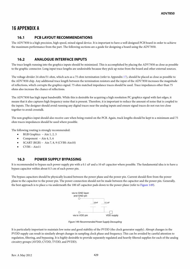
ADV7850
Rev. A May 2012 429
16 APPENDIX A
16.1 PCB LAYOUT RECOMMENDATIONS The ADV7850 is a high precision, high speed, mixed signal device. It is important to have a well designed PCB board in order to achieve the maximum performance from the part. The following sections are a guide for designing a board using the ADV7850.
16.2 ANALOGUE INTERFACE INPUTS The trace length running into the graphics inputs should be minimized. This is accomplished by placing the ADV7850 as close as possible to the graphic connector. Long input trace lengths are undesirable because they pick up noise from the board and other external sources. The voltage divider 24 ohm/51 ohm, which acts as a 75 ohm termination (refer to Appendix 17), should be placed as close as possible to the ADV7850 chip. Any additional trace length between the termination resistors and the input of the ADV7850 increases the magnitude of reflections, which corrupts the graphics signal. 75 ohm matched impedance traces should be used. Trace impedances other than 75 ohms also increase the chance of reflections. The ADV7850 has high input bandwidth. While this is desirable for acquiring a high resolution PC graphics signal with fast edges, it means that it also captures high frequency noise that is present. Therefore, it is important to reduce the amount of noise that is coupled to the inputs. The designer should avoid running any digital traces near the analog inputs and ensure signal traces do not run too close together to avoid crosstalk. The non graphics input should also receive care when being routed on the PCB. Again, track lengths should be kept to a minimum and 75 ohm traces impedances should be used where possible. The following routing is strongly recommended:
• RGB Graphics − Ain 1, 2, 3 • Component − Ain 4, 5, 6 • SCART (RGB) − Ain 7, 8, 9 (CVBS-Ain10) • CVBS – Ain11
16.3 POWER SUPPLY BYPASSING It is recommended to bypass each power supply pin with a 0.1 uF and a 10 nF capacitor where possible. The fundamental idea is to have a bypass capacitor within about 0.5 cm of each power pin. The bypass capacitors should be physically located between the power plane and the power pin. Current should flow from the power plane to the capacitor to the power pin. The power connection should not be made between the capacitor and the power pin. Generally, the best approach is to place a via underneath the 100 nF capacitor pads down to the power plane (refer to Figure 149).
Figure 149: Recommended Power Supply Decoupling It is particularly important to maintain low noise and good stability of the PVDD (the clock generator supply). Abrupt changes in the PVDD supply can result in similarly abrupt changes in sampling clock phase and frequency. This can be avoided by careful attention to regulation, filtering, and bypassing. It is highly desirable to provide separately regulated and heavily filtered supplies for each of the analog circuitry groups (AVDD, CVDD, TVDD, and PVDD).
10nF 0.1uF
via to GND layerand GND pin
via to VDD pin VDD supply

ADV7850
Rev. A May 2012 430
Some graphic controllers use substantially different levels of power when active (during active picture time) and when idle (during horizontal and vertical synchronization periods). This can result in a measurable change in the voltage supplied to the analog supply regulator, which can in turn produce changes in the regulated analog supply voltage. This can be mitigated by regulating the analog supply, or at least PVDD, from a separate, cleaner, power source. It is also recommended to use a single ground plane for the entire board. Repeatedly, experience has shown that the noise performance is the same or better with a single ground plane. Using multiple ground planes can be detrimental because each separate ground plane is smaller and long ground loops can result. In some cases, using separate ground planes is unavoidable. For those cases, it is recommended to place, at least, a single ground plane under the ADV7850.It is important to place components wisely because the current loops are much longer when using split ground planes as the current takes the path of least resistance. Example of a current loop: Power plane => ADV7850 => digital output trace => digital data receiver => digital ground plane => analog ground plane.
16.3.1 Power Supply Sequencing
16.3.1.1 Power Up Sequence
The recommended power up sequence of the ADV7850 is as follows: • 3.3 V supplies • 1.8 V supplies
Notes:
• Reset should be held low while the supplies are being powered up • 3.3 V supplies should be powered up first • 1.8 V supplies should be powered up after 3.3 V supplies are established
Figure 150: Recommended Power Up Sequence
Alternatively, the ADV7850 may be powered up by asserting all voltage supplies simultaneously. Note: In this case, care must be taken to ensure that a lower rated supply does not go above a higher rated supply level, as the supplies are being established.
16.3.1.2 Power Down Sequence The ADV7850 supplies may be de-asserted simultaneously as long as a higher rated supply does not go below a lower rated supply.
3 .3 V S U P P L IE SP O W E R -U P
POW
ER S
UPPL
Y (V
)
3 .3 V S U P P L IE S
1 .8 V S U P P L IE S
1 .8 V S U P P L IE SP O W E R -U P
3 .3 V
1 .8 V

ADV7850
Rev. A May 2012 431
16.4 DIGITAL OUTPUTS (DATA AND CLOCKS) The trace length that the digital outputs have to drive should be minimized. Longer traces have higher capacitance, which requires more current, which can cause more internal digital noise. Shorter traces reduce the possibility of reflections. Adding a series resistor of a value between 50 to 200 ohms can suppress reflections, reduce EMI, and reduce the current spikes inside the ADV7850. If series resistors are used, they should be placed as close as possible to the ADV7850 pins and the trace impedance for these signals should match that of the termination resistors selected. If possible, the capacitance that each of the digital outputs drives should be limited to is less than 15 pF. This can be accomplished easily by keeping traces short and by connecting the outputs to only one device. Loading the outputs with excessive capacitance increases the current transients inside the ADV7850, creating more digital noise on its power supplies.
16.5 DIGITAL INPUTS The following digital inputs on the ADV7850 are 3.3 V inputs that are 5.0 V tolerant:
• HS_IN1/TRI5 • VS_IN1/TRI6 • HS_IN2/TRI7 • VS_IN2/TRI8 • DDCA_SCL • DDCA_SDL • DDCB_SCL • DDCB_SDA • DDCC_SCL • DDCC_SDA • DDCD_SCL • DDCD_SDA • VGA_SCL • VGA_SDA
Any noise that gets onto the HSync and VS inputs trace will add jitter to the system. Therefore, the trace length should be minimized, and digital or other high frequency traces should not be run near it.
16.6 XTAL AND LOAD CAP VALUE SELECTION The ADV7850 uses a 27 MHz crystal. Figure 151 shows an example of a reference clock circuit for the ADV7850. Special care must be taken when using a crystal circuit to generate the reference clock for the ADV7850. Small variations in reference clock frequency can cause auto detection issues and impair the ADV7850 performance.
Figure 151: Crystal Circuit
These guidelines are followed to ensure correct operation:
• Use the correct frequency crystal, which is 27 MHz. Tolerance should be 50 ppm or better. • Know the Cload for the crystal part number selected. The value of capacitors C1 and C2 must be matched to the Cload for the
47pF 47pF
XTAL
C1 C2
27 MHz

ADV7850
Rev. A May 2012 432
specific crystal part number in the user system. To find C1 and C2, use the following formula: C1 = C2 = 2(Cload – Cstray)- Cpg where Cstray is usually 2 to 3 pF, depending on board traces and Cpg (pin-to-ground-capacitance) is 4 pF for the ADV7850. Example: Cload = 30 pF, C1 = 50 pF, C2 = 50 pF (in this case, 47 pF is the nearest real-life cap value to 50 pF)

ADV7850
Rev. A May 2012 433
17 APPENDIX B
17.1 ADV7850 TYPICAL CONNECTION DIAGRAMS
Figure 152: ADV7850 Analog Input Connections (1)

ADV7850
Rev. A May 2012 434
Figure 153: ADV7850 Analog Input Connections (2)

ADV7850
Rev. A May 2012 435
Figure 154: ADV7850 HDMI Input Connections (1)

ADV7850
Rev. A May 2012 436
Figure 155: ADV7850 HDMI Input Connections (2)
Figure 156: ADV7850 HDMI Output Connections

ADV7850
Rev. A May 2012 437
Figure 157: ADV7850 Audio Connections
Figure 158: ADV7850 Crystal and SPI EEPROM Connections

ADV7850
Rev. A May 2012 438
Figure 159: ADV7850 DDR2 Memory Connections

ADV7850
Rev. A May 2012 439
Figure 160: ADV7850 Power Supply Connections
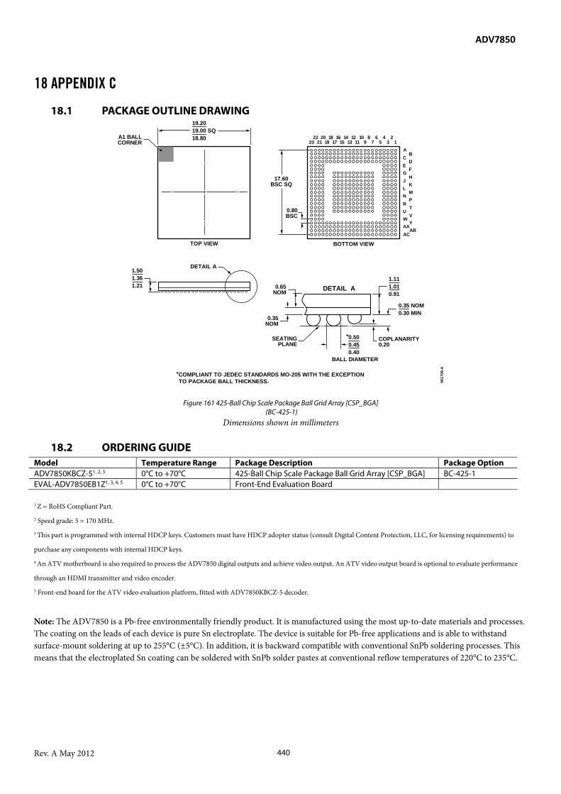
ADV7850
Rev. A May 2012 440
18 APPENDIX C
18.1 PACKAGE OUTLINE DRAWING
Figure 161 425-Ball Chip Scale Package Ball Grid Array [CSP_BGA] (BC-425-1)
Dimensions shown in millimeters
18.2 ORDERING GUIDE Model Temperature Range Package Description Package Option ADV7850KBCZ-51, 2, 3 0°C to +70°C 425-Ball Chip Scale Package Ball Grid Array [CSP_BGA] BC-425-1 EVAL-ADV7850EB1Z1, 3, 4, 5 0°C to +70°C Front-End Evaluation Board 1 Z = RoHS Compliant Part.
2 Speed grade: 5 = 170 MHz.
3 This part is programmed with internal HDCP keys. Customers must have HDCP adopter status (consult Digital Content Protection, LLC, for licensing requirements) to
purchase any components with internal HDCP keys.
4 An ATV motherboard is also required to process the ADV7850 digital outputs and achieve video output. An ATV video output board is optional to evaluate performance
through an HDMI transmitter and video encoder.
5 Front-end board for the ATV video evaluation platform, fitted with ADV7850KBCZ-5 decoder.
Note: The ADV7850 is a Pb-free environmentally friendly product. It is manufactured using the most up-to-date materials and processes. The coating on the leads of each device is pure Sn electroplate. The device is suitable for Pb-free applications and is able to withstand surface-mount soldering at up to 255°C (±5°C). In addition, it is backward compatible with conventional SnPb soldering processes. This means that the electroplated Sn coating can be soldered with SnPb solder pastes at conventional reflow temperatures of 220°C to 235°C.
*COMPLIANT TO JEDEC STANDARDS MO-205 WITH THE EXCEPTIONTO PACKAGE BALL THICKNESS. 06
1708
-A
0.80BSC
AB
CD
EF
GH
JK
LM
NP
R
151714
1312
1110
98
76
54
32
1
BOTTOM VIEW
17.60BSC SQ
161921
182023
22
TU
VW
YAA
ABAC
0.35 NOM0.30 MIN
0.65NOM
0.35NOM
DETAIL A
TOP VIEW
DETAIL A
COPLANARITY0.20
*0.500.450.40
BALL DIAMETER
SEATINGPLANE
19.2019.00 SQ18.80A1 BALL
CORNER
1.501.361.21
1.111.010.91

ADV7850
Rev. A May 2012 441
19 APPENDIX D
19.1 RECOMMENDED UNUSED PIN CONFIGURATIONS
Table 108: Recommended Configuration of Unused Pins Location Mnemonic Type Recommended Configuration if Not Used A1 GND Ground Ground A2 GND Ground Ground A3 GND Ground Ground A4 RXB_2+ HDMI Input Float this pin A5 RXB_1+ HDMI Input Float this pin A6 RXB_0+ HDMI Input Float this pin A7 RXB_C+ HDMI Input Float this pin A8 ARC_B HDMI Output Float this pin A9 TVDD Power This pin is always connected to Terminator supply voltage (3.3 V) A10 RXC_2+ HDMI Input Float this pin A11 RXC_1+ HDMI Input Float this pin A12 RXC_0+ HDMI Input Float this pin A13 RXC_C+ HDMI Input Float this pin A14 ARC_C HDMI Output Float this pin A15 GND Ground Ground A16 RXD_2+ HDMI Input Float this pin A17 RXD_1+ HDMI Input Float this pin A18 RXD_0+ HDMI Input Float this pin A19 RXD_C+ HDMI Input Float this pin A20 ARC_D HDMI Output Float this pin A21 GND Ground Ground A22 GND Ground Ground A23 GND Ground Ground B1 ARC_A HDMI Output Float this pin B2 HPA_A Miscellaneous digital Float this pin B3 GND Ground Ground B4 RXB_2- HDMI Input Float this pin B5 RXB_1- HDMI Input Float this pin B6 RXB_0- HDMI Input Float this pin B7 RXB_C- HDMI Input Float this pin B8 HPA_B Miscellaneous digital Float this pin B9 TVDD Power This pin is always connected to Terminator supply voltage (3.3 V) B10 RXC_2- HDMI Input Float this pin B11 RXC_1- HDMI Input Float this pin B12 RXC_0- HDMI Input Float this pin B13 RXC_C- HDMI Input Float this pin B14 HPA_C Miscellaneous digital Float this pin B15 GND Ground Ground B16 RXD_2- HDMI Input Float this pin B17 RXD_1- HDMI Input Float this pin B18 RXD_0- HDMI Input Float this pin B19 RXD_C- HDMI Input Float this pin B20 HPA_D Miscellaneous digital Float this pin B21 GND Ground Ground B22 ACMUXOUT_R Analog Audio Output Float this pin B23 ACMUXOUT_L Analog Audio Output Float this pin C1 RXA_C+ HDMI Input Float this pin C2 RXA_C- HDMI Input Float this pin C3 CVDD Power This pin is always connected to Comparator supply voltage (1.8 V)

ADV7850
Rev. A May 2012 442
Location Mnemonic Type Recommended Configuration if Not Used C4 GND Ground Ground C5 GND Ground Ground C6 GND Ground Ground C7 GND Ground Ground C8 VDD_EEPROM Power This pin must be decoupled to GND with a 100nF capacitor. C9 TVDD Power This pin is always connected to Terminator supply voltage (3.3 V) C10 TVDD Power This pin is always connected to Terminator supply voltage (3.3 V) C11 TVDD Power This pin is always connected to Terminator supply voltage (3.3 V) C12 TVDD Power This pin is always connected to Terminator supply voltage (3.3 V) C13 TVDD Power This pin is always connected to Terminator supply voltage (3.3 V) C14 TVDD Power This pin is always connected to Terminator supply voltage (3.3 V) C15 GND Ground Ground C16 TVDD Power This pin is always connected to Terminator supply voltage (3.3 V) C17 TVDD Power This pin is always connected to Terminator supply voltage (3.3 V) C18 TVDD Power This pin is always connected to Terminator supply voltage (3.3 V) C19 TVDD Power This pin is always connected to Terminator supply voltage (3.3 V) C20 GND Ground Ground C21 GND Ground Ground C22 ACMUXIN_1R Analog Audio Input Float this pin C23 ACMUXIN_1L Analog Audio Input Float this pin D1 RXA_0+ HDMI Input Float this pin D2 RXA_0- HDMI Input Float this pin D3 CVDD Power This pin is always connected to Comparator supply voltage (1.8 V) D4 RXD_5V HDMI Input. This pin should be tied to 5V D5 VGA_5V VGA Input Float this pin D6 DDCA_SCL HDMI Input Connect this pin to ground via a 10k ohm resistor D7 DDCA_SDA HDMI Input Float this pin D8 DDCB_SCL HDMI Input Connect this pin to ground via a 10k ohm resistor D9 DDCB_SDA HDMI Input Float this pin D10 DDCC_SCL HDMI Input Connect this pin to ground via a 10k ohm resistor D11 DDCC_SDA HDMI Input Float this pin D12 DDCD_SCL HDMI Input Connect this pin to ground via a 10k ohm resistor D13 DDCD_SDA HDMI Input Float this pin D14 VREG Voltage regulator
output This pin must be decoupled to GND via 1uF capacitor
D15 GND Ground Ground D16 VGA_SCL Miscellaneous digital Connect this pin to ground via a 10k ohm resistor D17 VGA_SDA Miscellaneous digital Float this pin D18 TVDD Power This pin is always connected to Terminator supply voltage (3.3 V) D19 AC_AVDD Power This pin is always connected to the Audio block supply (3.3V) D20 AC_AVDD Power This pin is always connected to the Audio block supply (3.3V) D21 AC_AVDD Power This pin is always connected to the Audio block supply (3.3V) D22 ACMUXIN_2R Analog Audio Input Float this pin D23 ACMUXIN_2L Analog Audio Input Float this pin E1 RXA_1+ HDMI Input Float this pin E2 RXA_1- HDMI Input Float this pin E3 CVDD Power This pin is always connected to Comparator supply voltage (1.8 V) E4 RXC_5V HDMI Input This pin should be tied to 5 V E20 GND Ground Ground E21 GND Ground Ground E22 ACMUXIN_3R Analog Audio Input Float this pin E23 ACMUXIN_3L Analog Audio Input Float this pin F1 RXA_2+ HDMI Input Float this pin F2 RXA_2- HDMI Input Float this pin F3 CVDD Power This pin is always connected to Comparator supply voltage (1.8 V)

ADV7850
Rev. A May 2012 443
Location Mnemonic Type Recommended Configuration if Not Used F4 RXB_5V HDMI Input This pin should be tied to 5 V F20 PLL_LF Miscellaneous Analog This pin is always connected to the external PLL loop filter circuit F21 GND Ground Ground F22 ACMUXIN_4R Analog Audio Input Float this pin F23 ACMUXIN_4L Analog Audio Input Float this pin G1 TVDD Power This pin is always connected to Terminator supply voltage (3.3 V) G2 TVDD Power This pin is always connected to Terminator supply voltage (3.3 V) G3 TVDD Power This pin is always connected to Terminator supply voltage (3.3 V) G4 TVDD Power This pin is always connected to Terminator supply voltage (3.3 V) G7 GND Ground Ground G8 TEST1 Test Float this Pin G9 CVDD Power This pin is always connected to Comparator supply voltage (1.8 V) G10 CVDD Power This pin is always connected to Comparator supply voltage (1.8 V) G11 CVDD Power This pin is always connected to Comparator supply voltage (1.8 V) G12 CVDD Power This pin is always connected to Comparator supply voltage (1.8 V) G13 CVDD Power This pin is always connected to Comparator supply voltage (1.8 V) G14 CVDD Power This pin is always connected to Comparator supply voltage (1.8 V) G15 CVDD Power This pin is always connected to Comparator supply voltage (1.8 V) G16 GND Ground Ground G17 GND Ground Ground G20 AC_AVDD Power This pin is always connected to the Audio block supply (3.3V) G21 GND Ground Ground G22 ACMUXIN_5R Analog Audio Input Float this pin G23 ACMUXIN_5L Analog Audio Input Float this pin H1 EP_MISO Digital Output Float this pin H2 EP_MOSI Digital Input Float this pin H3 SPDIF_IN Miscellaneous digital Float this pin H4 RXA_5V HDMI Input This pin should be tied to 5 V H7 GND Ground Ground H8 GND Ground Ground H9 GND Ground Ground H10 GND Ground Ground H11 GND Ground Ground H12 GND Ground Ground H13 GND Ground Ground H14 GND Ground Ground H15 GND Ground Ground H16 GND Ground Ground H17 GND Ground Ground H20 GND Ground Ground H21 GND Ground Ground H22 FILTA Miscellaneous analog This pin is always connected to 10 uF and 0.1 uF decoupling caps to
GND if using audio codec. Can be left floating if Audio Codec is not used.
H23 VREF_AUDIO Miscellaneous analog This pin is always connected to 47 uF and 0.1 uF decoupling caps to GND if using audio codec. Can be left floating if Audio Codec is not used.
J1 EP_CSB Miscellaneous digital Float this pin J2 EP_SCK Miscellaneous digital Float this pin J3 SHARED_EDID Miscellaneous digital Float this pin J4 RESET Miscellaneous digital This level should be controlled by an external processor J7 GND Ground Ground J8 GND Ground Ground J9 GND Ground Ground J10 GND Ground Ground

ADV7850
Rev. A May 2012 444
Location Mnemonic Type Recommended Configuration if Not Used J11 GND Ground Ground J12 GND Ground Ground J13 GND Ground Ground J14 GND Ground Ground J15 GND Ground Ground J16 GND Ground Ground J17 GND Ground Ground J20 AC_AVDD Power This pin is always connected to the Audio block supply (3.3V) J21 GND Ground Ground J22 ISET Miscellaneous analog Float this pin J23 FILTD Miscellaneous analog This pin is always connected to 47 uF and 0.1 uF decoupling caps to
GND if using audio codec. Can be left floating if Audio Codec is not used.
K1 GND Ground Ground K2 GND Ground Ground K3 DVDDIO Power This pin is always connected to the Digital IO supply voltage (3.3 V) K4 DVDDIO Power This pin is always connected to the Digital IO supply voltage (3.3 V) K7 VDD Power This pin is always connected to Digital core supply voltage (1.8 V) K8 GND Ground Ground K9 GND Ground Ground K10 GND Ground Ground K11 GND Ground Ground K12 GND Ground Ground K13 GND Ground Ground K14 GND Ground Ground K15 GND Ground Ground K16 GND Ground Ground K17 GND Ground Ground K20 AC_AVDD Power This pin is always connected to the Audio block supply (3.3V) K21 AC_AVDD Power This pin is always connected to the Audio block supply (3.3V) K22 AC_DACOut_R Analog Audio Output Float this pin K23 AC_DACOut_L Analog Audio Output Float this pin L1 HA_AP5 HDMI Output Float this pin L2 HA_SCLK HDMI Output Connect to ground via 10k resistor L3 INT1 Miscellaneous digital Float this pin L4 SDA Miscellaneous digital This pin is always connected to the I2C data line of a control
processor L7 VDD Power This pin is always connected to Digital core supply voltage (1.8 V) L8 GND Ground Ground L9 GND Ground Ground L10 GND Ground Ground L11 GND Ground Ground L12 GND Ground Ground L13 GND Ground Ground L14 GND Ground Ground L15 GND Ground Ground L16 GND Ground Ground L17 GND Ground Ground L20 AC_AVDD Power This pin is always connected to the Audio block supply (3.3V) L21 AC_AVDD Power This pin is always connected to the Audio block supply (3.3V) L22 HPOUT_R Analog Audio Output Float this pin L23 HPOUT_L Analog Audio Output Float this pin M1 HA_AP4 HDMI Output Float this pin M2 HA_AP3 HDMI Output Float this pin M3 INT2 Miscellaneous digital Float this pin

ADV7850
Rev. A May 2012 445
Location Mnemonic Type Recommended Configuration if Not Used M4 SCL Miscellaneous digital This pin is always connected to the I2C clock line of a control
processor M7 VDD Power This pin is always connected to Digital core supply voltage (1.8 V) M8 GND Ground Ground M9 GND Ground Ground M10 GND Ground Ground M11 GND Ground Ground M12 GND Ground Ground M13 GND Ground Ground M14 GND Ground Ground M15 GND Ground Ground M16 GND Ground Ground M17 GND Ground Ground M20 AC_AVDD Audio block supply
(3.3V)
M21 GND Ground Ground M22 GND Ground Ground M23 GND Ground Ground N1 HA_AP2 HDMI Output Float this pin N2 HA_AP1 HDMI Output Float this pin
N3 AC_MCLK Miscellaneous digital This pin should be connected to an oscillator or MCLK source when using audio codec. If Audio Codec is not in use, Float this pin
N4 AC_LRCLK Miscellaneous digital Float this pin N7 VDD Power This pin is always connected to Digital core supply voltage (1.8 V) N8 GND Ground Ground N9 GND Ground Ground N10 GND Ground Ground N11 GND Ground Ground N12 GND Ground Ground N13 GND Ground Ground N14 GND Ground Ground N15 GND Ground Ground N16 GND Ground Ground N17 GND Ground Ground N20 PVDD Power This pin is always connected to PLL supply voltage (1.8 V) N21 PVDD Power This pin is always connected to PLL supply voltage (1.8 V) N22 XTALN Miscellaneous analog This pin is always connected to 27MHz crystal N23 XTALP Miscellaneous analog This pin is always connected to 27MHz crystal or external clock P1 HA_AP0 HDMI Output Float this pin P2 HA_MCLKOUT HDMI Output Float this pin P3 AC_SDI Miscellaneous digital Float this pin P4 AC_SCLK Miscellaneous digital Float this pin P7 VDD Supply This pin is always connected to Digital core supply voltage (1.8 V) P8 GND Ground Ground P9 GND Ground Ground P10 GND Ground Ground P11 GND Ground Ground P12 GND Ground Ground P13 GND Ground Ground P14 GND Ground Ground P15 GND Ground Ground P16 GND Ground Ground P17 GND Ground Ground P20 GND Ground Ground

ADV7850
Rev. A May 2012 446
Location Mnemonic Type Recommended Configuration if Not Used P21 GND Ground Ground P22 GND Ground Ground P23 GND Ground Ground R1 TTX_SCLK Miscellaneous digital Float this pin R2 TTX_MOSI Miscellaneous digital Float this pin R3 TTX_MISO Miscellaneous digital Float this pin
R4 TTX_CSB Miscellaneous digital Float this pin R7 VDD Power This pin is always connected to Digital core supply voltage (1.8 V) R8 GND Ground Ground R9 GND Ground Ground R10 GND Ground Ground R11 GND Ground Ground R12 GND Ground Ground R13 GND Ground Ground R14 GND Ground Ground R15 GND Ground Ground R16 GND Ground Ground R17 GND Ground Ground R20 GND Ground Ground R21 GND Ground Ground R22 REFN Miscellaneous analog Always used as the internal voltage reference output. R23 REFP Miscellaneous analog Always used as the internal voltage reference output. T1 DVDDIO Power This pin is always connected to the Digital IO supply voltage (3.3 V) T2 DVDDIO Power This pin is always connected to the Digital IO supply voltage (3.3 V) T3 GND Ground Ground T4 GND Ground Ground T7 VDD Power This pin is always connected to Digital core supply voltage (1.8 V) T8 GND Ground Ground T9 GND Ground Ground T10 GND Ground Ground T11 GND Ground Ground T12 GND Ground Ground T13 GND Ground Ground T14 GND Ground Ground T15 GND Ground Ground T16 GND Ground Ground T17 GND Ground Ground T20 AVDD Power This pin is always connected to the Analog supply voltage (1.8 V) T21 AVDD Power This pin is always connected to the Analog supply voltage (1.8 V) T22 AVDD Power This pin is always connected to the Analog supply voltage (1.8 V) T23 AVDD Power This pin is always connected to the Analog supply voltage (1.8 V) U1 TX_AVDD Power This pin is always connected to the HDMI Tx Analog Supply (1.8V) U2 TX_AVDD Power This pin is always connected to the HDMI Tx Analog Supply (1.8V) U3 GND Ground Ground U4 TX_DDC_SCL Miscellaneous digital Float this pin U7 VDD Power This pin is always connected to Digital core supply voltage (1.8 V) U8 VDD Power This pin is always connected to Digital core supply voltage (1.8 V) U9 VDD Power This pin is always connected to Digital core supply voltage (1.8 V) U10 VDD Power This pin is always connected to Digital core supply voltage (1.8 V) U11 VDD Power This pin is always connected to Digital core supply voltage (1.8 V) U12 VDD Power This pin is always connected to Digital core supply voltage (1.8 V) U13 VDD Power This pin is always connected to Digital core supply voltage (1.8 V) U14 TEST2 Test Float this pin

ADV7850
Rev. A May 2012 447
Location Mnemonic Type Recommended Configuration if Not Used U15 GND Ground Ground U16 GND Ground Ground U17 GND Ground Ground U20 AVIN13 Analog Video Input Float this pin U21 AVIN12 Analog Video Input Float this pin U22 AVIN11 Analog Video Input Float this pin U23 AVIN10 Analog Video Input Float this pin V1 TX_2+ HDMI Tx Output Float this pin V2 TX_2- HDMI Tx Output Float this pin V3 GND Ground Ground V4 TX_DDC_SDA Miscellaneous digital Float this pin V20 AVDD Power This pin is always connected to Analog supply voltage (1.8 V) V21 AVDD Power This pin is always connected to Analog supply voltage (1.8 V) V22 AVDD Power This pin is always connected to Analog supply voltage (1.8 V) V23 AVDD Power This pin is always connected to Analog supply voltage (1.8 V) W1 TX_1+ HDMI Tx Output Float this pin W2 TX_1- HDMI Tx Output Float this pin W3 GND Ground Ground W4 TX_HPD Miscellaneous digital Float this pin W20 GND Ground Ground W21 AVOUT2 Analog Video Output Float this pin W22 AVIN9 Analog Video Input Float this pin W23 AVIN8 Analog Video Input Float this pin Y1 TX_0+ HDMI Tx Output Float this pin Y2 TX_0- HDMI Tx Output Float this pin Y3 GND Ground Ground Y4 GND Ground Ground Y5 A7 SDRAM Interface Float this pin Y6 A3 SDRAM Interface Float this pin Y7 A10 SDRAM Interface Float this pin Y8 BA0 SDRAM Interface Float this pin Y9 CKE SDRAM Interface Float this pin Y10 GND Ground Ground Y11 DQ6 SDRAM Interface Tie to ground via a 4k7 resistor Y12 DQ7 SDRAM Interface Tie to ground via a 4k7 resistor Y13 DQ0 SDRAM Interface Tie to ground via a 4k7 resistor Y14 DQ8 SDRAM Interface Tie to ground via a 4k7 resistor Y15 UDQS SDRAM Interface Tie to ground via a 4k7 resistor Y16 SDVDD Power This pin is always connected to the Memory interface supply (1.8V) Y17 SAVDD Power This pin is always connected to the SDRAM interface supply (1.8V) Y18 TRI1 Miscellaneous analog Float this pin Y19 TRI2 Miscellaneous analog Float this pin Y20 GND Ground Ground Y21 AVOUT1 Analog Video Output Float this pin Y22 SYNC3 Miscellaneous analog Float this pin Y23 AVIN7 Analog Video Input Float this pin AA1 TX_C+ HDMI Tx Output Float this pin AA2 TX_C- HDMI Tx Output Float this pin AA3 TX_AVDD Power This pin is always connected to the HDMI Tx Analog Supply (1.8V) AA4 GND Ground Ground AA5 A9 SDRAM Interface Float this pin AA6 A5 SDRAM Interface Float this pin AA7 A1 SDRAM Interface Float this pin AA8 BA1 SDRAM Interface Float this pin AA9 WE SDRAM Interface Float this pin

ADV7850
Rev. A May 2012 448
Location Mnemonic Type Recommended Configuration if Not Used AA10 GND Ground Ground AA11 DQ4 SDRAM Interface Tie to ground via a 4k7 resistor AA12 DQ5 SDRAM Interface Tie to ground via a 4k7 resistor AA13 DQ2 SDRAM Interface Tie to ground via a 4k7 resistor AA14 DQ11 SDRAM Interface Tie to ground via a 4k7 resistor AA15 UDQSN SDRAM Interface Float this pin AA16 SDVDD Power This pin is always connected to the Memory interface supply (1.8V) AA17 GND Ground Ground AA18 HS_IN1/TRI7 Miscellaneous Analog Float this pin AA19 VS_IN1/TRI8 Miscellaneous Analog Float this pin AA20 GND Ground Ground AA21 TRI3 Miscellaneous Analog Float this pin AA22 HS_IN2/TRI5 Miscellaneous Analog Float this pin AA23 VS_IN2/TRI6 Miscellaneous Analog Float this pin AB1 GND Ground Ground AB2 TX_PVDD Power This pin is always connected to the HDMI Tx digital supply (1.8V) AB3 TX_PLVDD Voltage regulator
output Connect decoupling capacitor between this pin and ground
AB4 SDVDD Power This pin is always connected to the Memory interface supply (1.8V) AB5 A11 SDRAM Interface Float this pin AB6 A6 SDRAM Interface Float this pin AB7 A2 SDRAM Interface Float this pin AB8 CAS SDRAM Interface Float this pin AB9 RAS SDRAM Interface Float this pin AB10 VREF SDRAM Interface Tie to SDVDD supply AB11 SDVDD Power This pin is always connected to the Memory interface supply (1.8V) AB12 LDQSN SDRAM Interface Float this pin AB13 DQ3 SDRAM Interface Tie to ground via a 4k7 resistor AB14 DQ10 SDRAM Interface Tie to ground via a 4k7 resistor AB15 DQ12 SDRAM Interface Tie to ground via a 4k7 resistor AB16 DQ14 SDRAM Interface Tie to ground via a 4k7 resistor AB17 GND Ground Ground AB18 SYNC1 Miscellaneous analog Float this pin AB19 AVIN3 Analog Video Input Float this pin AB20 GND Ground Ground AB21 SYNC2 Miscellaneous analog Float this pin AB22 AVIN6 Analog Video Input Float this pin AB23 TRI4 Miscellaneous analog Float this pin AC1 GND Ground Ground AC2 TX_RTERM Miscellaneous analog This pin is always connected to a 470R resistor to GND AC3 TX_VDD33 Miscellaneous analog Float this pin AC4 SDVDD Power This pin is always connected to the Memory interface supply (1.8V) AC5 A8 SDRAM Interface Float this pin AC6 A4 SDRAM Interface Float this pin AC7 A0 SDRAM Interface Float this pin AC8 CS SDRAM Interface Float this pin AC9 CKN SDRAM Interface Float this pin AC10 CK SDRAM Interface Float this pin AC11 SDVDD Power This pin is always connected to the Memory interface supply (1.8V) AC12 LDQS SDRAM Interface Tie to ground via a 4k7 resistor AC13 DQ1 SDRAM Interface Tie to ground via a 4k7 resistor AC14 DQ9 SDRAM Interface Tie to ground via a 4k7 resistor AC15 DQ15 SDRAM Interface Tie to ground via a 4k7 resistor AC16 DQ13 SDRAM Interface Tie to ground via a 4k7 resistor AC17 GND Ground Ground

ADV7850
Rev. A May 2012 449
Location Mnemonic Type Recommended Configuration if Not Used AC18 AVIN1 Analog Video Input Float this pin AC19 AVIN2 Analog Video Input Float this pin AC20 GND Ground Ground AC21 AVIN4 Analog Video Input Float this pin AC22 AVIN5 Analog Video Input Float this pin AC23 GND Ground Ground

ADV7850
Rev. A May 2012 450
LIST OF FIGURES Figure 1: Field Description Format ................................................................................................................................................................... 13 Figure 2: Functional Block Diagram ................................................................................................................................................................. 19 Figure 3: ADV7850 Pin Configuration ............................................................................................................................................................ 20 Figure 4: Required Hardware Configuration When Using +5 V from HDMI Source(s) to Provide EDID Support in Powered Off
State ............................................................................................................................................................................................................. 32 Figure 5: Analog Inputs Hardware Configuration ......................................................................................................................................... 42 Figure 6: Video Input Signal Level Prior to 24 Ohm to 51 Ohm Resistor Divider .................................................................................... 43 Figure 7: Video Input Signal Level After Voltage Clamps ............................................................................................................................. 43 Figure 8: SDP Clamping Overview ................................................................................................................................................................... 44 Figure 9: ADV7850 Typical Configurations .................................................................................................................................................... 45 Figure 10: ADV7850 Input Functional Diagram ............................................................................................................................................ 46 Figure 11: Synchronization Stripper Circuit ................................................................................................................................................... 51 Figure 12: D-Terminal Resistor Dividers ......................................................................................................................................................... 54 Figure 13: Trilevel Slicer ..................................................................................................................................................................................... 54 Figure 14: ADV7850 Fast Blanking Configuration ........................................................................................................................................ 64 Figure 15: Response of Anti Aliasing Filters .................................................................................................................................................... 68 Figure 16: Block Diagram of SDP ..................................................................................................................................................................... 69 Figure 17: SDP Gain Control Overview ........................................................................................................................................................... 82 Figure 18: 3D Comb and Motion Detection Operation................................................................................................................................. 87 Figure 19: Y Shaping Filter Flowchart .............................................................................................................................................................. 94 Figure 20: Y Shaping Filter Selection from No. 0 to No. 13 in Table 10...................................................................................................... 97 Figure 21: Y Shaping Filter Selection from No. 14 to 20 in Table 10 ........................................................................................................... 98 Figure 22: Y Shaping Filter Selection from No. 21 to 24 in Table 10 ........................................................................................................... 98 Figure 23: Y Shaping Filter Selection from No. 25 to 27 in Table 10 ........................................................................................................... 99 Figure 24: Y Shaping Filter Selection from No. 28 to 30 in Table 10 ........................................................................................................... 99 Figure 25: Y Shaping Filter Selection from No. 31 in Table 10 ................................................................................................................... 100 Figure 26: C Shaping Filter Flowchart ............................................................................................................................................................ 104 Figure 27: C Shaping Filter Selection No. 0 to 3 in Table 11 ....................................................................................................................... 106 Figure 28: C Shaping Filter Selection No. 4 to 13 in Table 11 ..................................................................................................................... 107 Figure 29: C Shaping Filter No. 14 to 18 in Table 11 ................................................................................................................................... 107 Figure 30: Split Filter Frequency Response .................................................................................................................................................... 108 Figure 31: IF Compensation Filter Responses 0 to 3 .................................................................................................................................... 109 Figure 32: IF Compensation Filter Responses 4 to 9 .................................................................................................................................... 109 Figure 33: LTI/CTI Operation Diagram ........................................................................................................................................................ 110 Figure 34: SECAM Signal Distortion .............................................................................................................................................................. 111 Figure 35: LTI Filter Response 0 ..................................................................................................................................................................... 111 Figure 36: LTI Filter Response 1 ..................................................................................................................................................................... 112 Figure 37: CTI Filter Response 0 ..................................................................................................................................................................... 113 Figure 38: CTI Filter Response 1 ..................................................................................................................................................................... 113 Figure 39: Peaking Block Diagram .................................................................................................................................................................. 115 Figure 40: Core Threshold in Horizontal Peaking ....................................................................................................................................... 116 Figure 41: Horizontal Peaking High-Pass Filter ........................................................................................................................................... 117 Figure 42: Horizontal Peaking Band-Pass Filter 1 ........................................................................................................................................ 117 Figure 43: Horizontal Peaking Band-Pass Filter 2 ........................................................................................................................................ 118 Figure 44: Peaking Controls ............................................................................................................................................................................. 119 Figure 45: Vertical Peaking Filter .................................................................................................................................................................... 120 Figure 46: Frame Synchronization Block Diagram ...................................................................................................................................... 121 Figure 47: HSync and VSync Timing Controls ............................................................................................................................................. 126 Figure 48: DE Timing Controls ....................................................................................................................................................................... 131 Figure 49: Single CSC Channel ........................................................................................................................................................................ 132
ADV7850
Rev. A May 2012 451
Figure 50: Functional Block Diagram of HDMI Core ................................................................................................................................. 136 Figure 51: SPI EEPROM Data Image Structure ............................................................................................................................................ 146 Figure 52: Port A E-EDID Structure and Mapping ...................................................................................................................................... 147 Figure 53: Port B E-EDID Structure and Mapping for SPA Located in E-EDID Block 1 ....................................................................... 148 Figure 54: Monitoring TMDS Clock Frequency ........................................................................................................................................... 158 Figure 55: HDMI Video FIFO ......................................................................................................................................................................... 160 Figure 56: HDCP ROM Access After Power Up ........................................................................................................................................... 168 Figure 57: HDCP ROM Access After KSV Update from the Transmitter ................................................................................................ 168 Figure 58: Horizontal Timing Parameters ..................................................................................................................................................... 171 Figure 59: Vertical Parameters for Field 0 ..................................................................................................................................................... 174 Figure 60: Vertical Parameters for Field 1 ..................................................................................................................................................... 176 Figure 61: Audio Processor Block Diagram .................................................................................................................................................. 178 Figure 62: Audio FIFO ...................................................................................................................................................................................... 179 Figure 63: Monitoring Audio Packet Type Processed by ADV7850 .......................................................................................................... 183 Figure 64: Timing Audio Data Output in I2S Mode ..................................................................................................................................... 186 Figure 65: Timing Audio Data Output in Right Justified Mode ................................................................................................................. 186 Figure 66: Timing Audio Data Output in Left Justified Mode ................................................................................................................... 186 Figure 67: IEC 60958 Sub-frame Timing Diagram ....................................................................................................................................... 186 Figure 68: AES3 Sub-frame Timing Diagram ............................................................................................................................................... 187 Figure 69: AES3 Stream Timing Diagram ..................................................................................................................................................... 187 Figure 70: DSD Timing Diagram1 .................................................................................................................................................................. 188 Figure 71: DST Timing Diagram for DST_DOUBLE = 0 .......................................................................................................................... 189 Figure 72: DST Timing Diagram for DST_DOUBLE = 1 ........................................................................................................................... 190 Figure 73: Reading Valid Channel Status Flags............................................................................................................................................. 197 Figure 74: YCbCr 4:2:2 Video Data Encapsulated in HDMI Stream .......................................................................................................... 221 Figure 75: Video Stream Output by HDMI Core for YCbCr 4:2:2 Input and UP_CONVERSION = 0 ................................................ 222 Figure 76: Configuring CP CSC Block ........................................................................................................................................................... 230 Figure 77: Single CSC Channel ........................................................................................................................................................................ 233 Figure 78: Component Processor Block Diagram ........................................................................................................................................ 241 Figure 79: Position of Voltage Clamp Window ............................................................................................................................................ 242 Figure 80: CP Automatic Gain Controls ........................................................................................................................................................ 245 Figure 81: Channel A, B, and C Automatic Value Selection ....................................................................................................................... 252 Figure 82: CP DATA Path Channel A (Y) for Analog Mode ...................................................................................................................... 255 Figure 83: CP Data Path Channel B/C (UV) for Analog Mode .................................................................................................................. 256 Figure 84: CP Data Path Channel A/B/C (RGB) for Analog Mode ........................................................................................................... 257 Figure 85: Sliced Signal Path ........................................................................................................................................................................... 258 Figure 86: External/HDMI Syncs Routing to CP Section ........................................................................................................................... 259 Figure 87: Final Sync Muxing Stage ............................................................................................................................................................... 262 Figure 88: SSPD Auto Detection Flowchart .................................................................................................................................................. 264 Figure 89: SSPD VSync and HSync Monitoring Operation ........................................................................................................................ 270 Figure 90: STDI Horizontal Locking Operation ........................................................................................................................................... 274 Figure 91: STDI HSync Monitoring Operation ............................................................................................................................................ 274 Figure 92: STDI Vertical Locking Operation ................................................................................................................................................ 275 Figure 93: STDI VSync Monitoring Operation............................................................................................................................................. 275 Figure 94: STDI Usage Flowchart ................................................................................................................................................................... 277 Figure 95: ADV7850 Simplified Synchronization Signal Processing Flow Diagram .............................................................................. 278 Figure 96: Synchronization Repositioning and Displayed Area ................................................................................................................. 279 Figure 97: HS Timing ........................................................................................................................................................................................ 281 Figure 98: 525i VS Timing ............................................................................................................................................................................... 289 Figure 99: 625i VS Timing ............................................................................................................................................................................... 290 Figure 100: 525p VS Timing ............................................................................................................................................................................ 291 Figure 101: 625p VS Timing ............................................................................................................................................................................ 292

ADV7850
Rev. A May 2012 452
Figure 102: 720p VS Timing ............................................................................................................................................................................ 293 Figure 103: 1080i VS Timing ........................................................................................................................................................................... 294 Figure 104: 1080p VS Timing .......................................................................................................................................................................... 295 Figure 105: Synchronization Lock Robustness Measurement .................................................................................................................... 297 Figure 106: Free Run Field Length Selection for Channel 1 and Channel 2 ............................................................................................. 303 Figure 107: WSS (625i) Waveform ................................................................................................................................................................. 315 Figure 108: CGMS (525i) Waveform .............................................................................................................................................................. 315 Figure 109: CCAP Waveform and Decoded Data Correlation ................................................................................................................... 316 Figure 110: VITC Waveform and Decoded Data Correlation .................................................................................................................... 317 Figure 111: VDP Interrupt Operation ............................................................................................................................................................ 331 Figure 112: VDP Access Over SPI ................................................................................................................................................................... 331 Figure 113: Audio Block ................................................................................................................................................................................... 333 Figure 114: Audio Codec Analog Inputs Hardware Configuration ........................................................................................................... 333 Figure 115: Audio Codec Mux Output Hardware Configuration .............................................................................................................. 334 Figure 116: High Level Overview of Analog Audio Mux Input/Mux Output Configuration ................................................................ 336 Figure 117: Audio PLL Loop Filter Components ......................................................................................................................................... 337 Figure 118: Audio Codec VREF AUDIO, FILTA and FILTD Configuration .......................................................................................... 338 Figure 119: Audio Codec DAC Output Hardware Configuration ............................................................................................................. 338 Figure 120: Audio Codec Headphone Output Hardware Configuration.................................................................................................. 339 Figure 121: DDR2 BIST Test Architecture .................................................................................................................................................... 346 Figure 122: Functional Block Diagram of HDMI Tx Core.......................................................................................................................... 349 Figure 123: Format of Video Data Input into HDMI Tx Core ................................................................................................................... 356 Figure 124: I2C Write Timing if GMP Data ................................................................................................................................................... 361 Figure 125: IEC60958 Sub Stream ................................................................................................................................................................... 367 Figure 126: AES3 Stream Format Input to ADV7850 .................................................................................................................................. 367 Figure 127: Timing of Standard I2S Stream Input to ADV7850 ................................................................................................................ 367 Figure 128: Timing for Right-Justified I2S Stream Input to ADV7850 ..................................................................................................... 368 Figure 129: Timing for Left-Justified I2S Stream Input to ADV7850 ........................................................................................................ 368 Figure 130: Timing for I2S Stream in 32-bit Mode ...................................................................................................................................... 368 Figure 131: Timing for I2S Stream in Left or Right-Justified and 32-bit Modes ...................................................................................... 368 Figure 132: Audio Clock Regeneration .......................................................................................................................................................... 370 Figure 133: Definition of Channel Status Bits 20 to 23 ................................................................................................................................ 377 Figure 134: Reading Sink EDID Through ADV7850 ................................................................................................................................... 381 Figure 135: HDCP Software Implementation ............................................................................................................................................... 386 Figure 136: ADV7850 Register Map Access through Main I2C Port ......................................................................................................... 388 Figure 137: Bus Data Transfer ......................................................................................................................................................................... 389 Figure 138: Read and Write Sequence ............................................................................................................................................................ 389 Figure 139: Current Address Read Sequence ................................................................................................................................................ 390 Figure 140: Internal E-EDID and HDCP Registers Access from Port A ................................................................................................... 390 Figure 141: Internal E-EDID and HDCP Registers Access from Port B ................................................................................................... 390 Figure 142: Internal E-EDID and HDCP Registers Access from Port C ................................................................................................... 391 Figure 143: Internal E-EDID and HDCP Registers Access from Port D .................................................................................................. 391 Figure 144: Level and Edge-sensitive Raw, Status and Interrupt Generation ........................................................................................... 396 Figure 145: AVI_INFO_RAW and AVI_INFO_ST Timing ....................................................................................................................... 397 Figure 146: NEW_AVI_INFO_RAW and NEW_AVI_INFO_ST Timing .............................................................................................. 397 Figure 147: Suggested Method of Handling afe_interrupt .......................................................................................................................... 401 Figure 148: Processing Trilevel Interrupts ..................................................................................................................................................... 426 Figure 149: Recommended Power Supply Decoupling ................................................................................................................................ 429 Figure 150: Recommended Power Up Sequence .......................................................................................................................................... 430 Figure 151: Crystal Circuit ............................................................................................................................................................................... 431 Figure 152: ADV7850 Analog Input Connections (1) ................................................................................................................................. 433 Figure 153: ADV7850 Analog Input Connections (2) ................................................................................................................................. 434

ADV7850
Rev. A May 2012 453
Figure 154: ADV7850 HDMI Input Connections (1) .................................................................................................................................. 435 Figure 155: ADV7850 HDMI Input Connections (2) .................................................................................................................................. 436 Figure 156: ADV7850 HDMI Output Connections ..................................................................................................................................... 436 Figure 157: ADV7850 Audio Connections .................................................................................................................................................... 437 Figure 158: ADV7850 Crystal and SPI EEPROM Connections ................................................................................................................. 437 Figure 159: ADV7850 DDR2 Memory Connections ................................................................................................................................... 438 Figure 160: ADV7850 Power Supply Connections ....................................................................................................................................... 439 Figure 161 425-Ball Chip Scale Package Ball Grid Array [CSP_BGA] (BC-425-1) Dimensions shown in millimeters ................... 440

ADV7850
Rev. A May 2012 454
LIST OF TABLES Table 1: Function Descriptions ......................................................................................................................................................................... 20 Table 2: Primary Mode and Video Standard Selection .................................................................................................................................. 36 Table 3: Vertical Frequencies Supported in HD Modes ................................................................................................................................ 40 Table 4: Manual Input Muxing ......................................................................................................................................................................... 48 Table 5: Recommended Video Signal to ADC Routing ................................................................................................................................. 49 Table 6: Available Inputs on Aout1 and Aout2 ............................................................................................................................................... 49 Table 7: D-Terminal Connector Characteristics (Trilevel) ........................................................................................................................... 53 Table 8: D-Terminal Connector Characteristics (Bilevel) ............................................................................................................................. 53 Table 9: Anti Alias Filter Frequency Characteristics ...................................................................................................................................... 68 Table 10: Y Shaping Filter Selection ................................................................................................................................................................ 95 Table 11: C Shaping Filter Selection ............................................................................................................................................................... 105 Table 12: CSC Coefficients ............................................................................................................................................................................... 132 Table 13: Selectable Coast Conditions ............................................................................................................................................................ 179 Table 14: Audio Outputs and Clocks ............................................................................................................................................................. 183 Table 15: Default Audio Output Pixel Port Mapping ................................................................................................................................. 184 Table 16: Audio Mappings for i2s_spdif_map_rot = 00, i2s_spdif_map_inv = 0 (Default)................................................................... 184 Table 17: Audio Mappings for i2s_spdif_map_rot = 00, i2s_spdif_map_inv = 1 .................................................................................... 184 Table 18: I2S/SPDIF Interface Description .................................................................................................................................................... 186 Table 19: DSD Interface Description .............................................................................................................................................................. 187 Table 20: Audio Mapping for dsd_map_rot = 00, dsd_map_inv = 0 (Default) ....................................................................................... 188 Table 21: Audio Mapping for dsd_map_rot = 00, dsd_map_inv = 1 ........................................................................................................ 188 Table 22: DST Interface Description .............................................................................................................................................................. 189 Table 23: HBR Interface Description .............................................................................................................................................................. 190 Table 24: Selectable Mute Conditions ............................................................................................................................................................ 193 Table 25: AVI InfoFrame Registers ................................................................................................................................................................ 202 Table 26: Audio InfoFrame Registers ............................................................................................................................................................. 203 Table 27: SPD InfoFrame Registers ................................................................................................................................................................ 204 Table 28: MPEG InfoFrame Registers ............................................................................................................................................................ 205 Table 29: VS InfoFrame Registers ................................................................................................................................................................... 205 Table 30: ACP Packet Registers ....................................................................................................................................................................... 207 Table 31: ISRC1 Packet Registers .................................................................................................................................................................... 208 Table 32: ISRC2 Packet Registers .................................................................................................................................................................... 209 Table 33: Gamut Metadata Packet Registers ................................................................................................................................................. 210 Table 34: Register Location for SHA_1 Hash Value ................................................................................................................................... 218 Table 35: KSV List Bytes .................................................................................................................................................................................. 218 Table 36: HDMI Flags in IO Map Register 0x60 ........................................................................................................................................... 223 Table 37: HDMI Flags in IO Map Register 0x65 ........................................................................................................................................... 223 Table 38: HDMI Flags in IO Map Register 0x6A .......................................................................................................................................... 223 Table 39: HDMI Flags in IO Map Register 0x6F .......................................................................................................................................... 223 Table 40: HDMI Flags in IO Map Register 0x74 ........................................................................................................................................... 223 Table 41: HDMI Flags in IO Map Register 0x79 ........................................................................................................................................... 224 Table 42: HDMI Flags in IO Map Register 0x7E .......................................................................................................................................... 224 Table 43: HDMI Flags in IO Map Register 0x83 ........................................................................................................................................... 224 Table 44: HDMI InfoFrame Checksum Error Flags in IO Map ................................................................................................................. 225 Table 45: AKSV Update Flags in IO Map Register 0x88 ............................................................................................................................. 225 Table 46: HDMI Flags in HDMI Map ............................................................................................................................................................ 225 Table 47: Automatic Input Color Space Selection ........................................................................................................................................ 232 Table 48: Automatic CSC Selection ................................................................................................................................................................ 232 Table 49: CSC Configuration for All CSC Modes Reported by csc_coeff_sel_rb .................................................................................... 233 Table 50: CSC Coefficients ............................................................................................................................................................................... 234

ADV7850
Rev. A May 2012 455
Table 51: OP_656_RANGE Description for Analog Front End Input Mode ........................................................................................... 250 Table 52: Settings Required to Support Extended Range Video Input ...................................................................................................... 253 Table 53: STDI Readback Values for SD, PR, and HD ................................................................................................................................ 277 Table 54: STDI Results for Graphics Standards ............................................................................................................................................ 278 Table 55: HSync Default Timing ..................................................................................................................................................................... 280 Table 56: HSync Default Timing (Continued 1) ........................................................................................................................................... 280 Table 57: HSync Default Timing (Continued 2) ........................................................................................................................................... 280 Table 58: HSync Default Timing (Continued 3) ........................................................................................................................................... 280 Table 59: VS Default Timing ........................................................................................................................................................................... 283 Table 60: FIELD Default Timing ..................................................................................................................................................................... 287 Table 61: Default Color Output Values (CP) ................................................................................................................................................ 303 Table 62: vbi_data_std[3:0] Values Corresponding to a Particular VBI Standard .................................................................................. 311 Table 63: Default Standards on Lines for Supported Interlaced and Progressive Standards ................................................................. 311 Table 64: Details of Manual Line Programming Registers .......................................................................................................................... 312 Table 65: Details of Full Field/Frame Programming Registers ................................................................................................................... 313 Table 66: VITC Readback Registers ................................................................................................................................................................ 317 Table 67: vdp_gs_vps_pdc_utc_cgmstb_data Readback Registers ............................................................................................................ 318 Table 68: CGMS Type B Readback Registers ................................................................................................................................................ 319 Table 69: Configuration VBI Standard to be Output on SPI Interface ...................................................................................................... 322 Table 70: Standard SPI Slave Mode Output Format .................................................................................................................................... 322 Table 71: Teletext SPI Slave Mode Output Format ...................................................................................................................................... 323 Table 72: CCAP SPI Slave Mode Output Format ......................................................................................................................................... 323 Table 73: WSS SPI Slave Mode Output Format ............................................................................................................................................ 323 Table 74: CGMS-A SPI Slave Mode Output Format .................................................................................................................................... 324 Table 75: CGMS-B SPI Slave Mode Output Format .................................................................................................................................... 324 Table 76: Format of Ancillary Packets ............................................................................................................................................................ 324 Table 77: Number of Bits in Each of Framing Codes ................................................................................................................................... 325 Table 78: Number of Data Words in Ancillary Data Packet for Some VBI Standards ........................................................................... 325 Table 79: VBI Standard Number and Line Numbers for Each VBI Type ................................................................................................. 326 Table 80: SPI Payload for TTXT...................................................................................................................................................................... 331 Table 81: Analog Audio Inputs to ADC and Analog Audio Outputs Connection Options................................................................... 333 Table 82 : TX Squelch Configuration Options .............................................................................................................................................. 351 Table 83: SPD InfoFrame Configuration Register ........................................................................................................................................ 352 Table 84: Spare Packet 1 Configuration Register .......................................................................................................................................... 353 Table 85: Spare Packet 2 Configuration Register .......................................................................................................................................... 354 Table 86: HDMI Tx Interrupt Bits in HDMI Tx Main Map Register 0x96 .............................................................................................. 355 Table 87: HDMI Tx Interrupt Bits in Main Map Register 0x97 ................................................................................................................. 355 Table 88: Status Bits in Main Map Register 0x42 .......................................................................................................................................... 355 Table 89: AVI InfoFrame Configuration Registers ...................................................................................................................................... 359 Table 90: MPEG InfoFrame Configuration Registers .................................................................................................................................. 360 Table 91: Gamut Metadata Packet Configuration Registers ....................................................................................................................... 361 Table 92: Valid Configuration for audio_mode[1:0] ................................................................................................................................... 362 Table 93: Audio Input Format Summary ....................................................................................................................................................... 363 Table 94: Valid Configuration for audioif_sf[2:0] ........................................................................................................................................ 369 Table 95: Recommended N and Expected CTS Values for 32 kHz Audio ................................................................................................ 372 Table 96: Recommended N and Expected CTS Values for 44.1 kHz and Multiples ............................................................................... 372 Table 97: Recommended N and Expected CTS Values for 48 kHz and Multiples .................................................................................. 373 Table 98: I2S Channel Status ADV7850 Register Map Location of Fixed Value ...................................................................................... 375 Table 99: Audio InfoFrame Configuration Registers ................................................................................................................................... 378 Table 100: ACP Packet Configuration Registers ........................................................................................................................................... 378 Table 101: ISRC1 Packet Configuration Registers ........................................................................................................................................ 379 Table 102: ISRC2 Packet Configuration Registers ........................................................................................................................................ 380

ADV7850
Rev. A May 2012 456
Table 103: KSV Fields Accessed From EDID Map ....................................................................................................................................... 384 Table 104: Register Maps and I2C Addresses ................................................................................................................................................ 388 Table 105: HDMI Interrupts Group 1 ............................................................................................................................................................ 403 Table 106: HDMI Interrupts Group 2 ............................................................................................................................................................ 403 Table 107: HDMI Interrupts Group 3 ............................................................................................................................................................ 404 Table 108: Recommended Configuration of Unused Pins .......................................................................................................................... 441
ADV7850
Rev. A May 2012 457
LIST OF EQUATIONS Equation 1: SDP Luma Gain Formula .............................................................................................................................................................. 83 Equation 2: SDP Chroma Gain Formula ......................................................................................................................................................... 84 Equation 3: TMDS Frequency in MHz (Measured After TMDS PLL) ...................................................................................................... 155 Equation 4: Unit Time of Horizontal Filter Measurements ........................................................................................................................ 169 Equation 5: Relationship Between MCLKOUT, MCLKFS_N, and fs ........................................................................................................ 191 Equation 6: CSC Channel A ............................................................................................................................................................................. 236 Equation 7: CSC Channel B ............................................................................................................................................................................. 236 Equation 8: CSC Channel C ............................................................................................................................................................................. 236 Equation 9: Hue in Degree Unit Applied to Chroma via cp_hue[7:0] Control ....................................................................................... 240 Equation 10: CP Manual Gain ......................................................................................................................................................................... 246 Equation 11: CP AGC Target Value ............................................................................................................................................................... 247 Equation 12: Peak Active Video Readback Value ......................................................................................................................................... 251 Equation 13: Relationship Between Audio Reference and TMDS Clocks ................................................................................................ 371 Equation 14: Restriction for N Value ............................................................................................................................................................. 371 Equation 15: Optimal N Value ........................................................................................................................................................................ 371 Equation 16: Relationship Between N and CTS ............................................................................................................................................ 371

ADV7850
Rev. A May 2012 458
REVISION HISTORY February 2012 Rev. 0 Initial version May 2012 Rev.A Removed Confidential from the document
Updated CP FreeRun controls Removed Section 13.15