advanced condensed matter i: solid state physics€¦ · advanced condensed matter i: solid state...
TRANSCRIPT

Advanced Condensed Matter I: Solid State Physics
Bernd v. Issendorff
February 10, 2017

Contents
1 Atomic Structure of Matter 31.1 Crystal Structure . . . . . . . . . . . . . . . . . . . . . . . . . . . . . . . . . . . . 3
1.1.1 Crystal lattice . . . . . . . . . . . . . . . . . . . . . . . . . . . . . . . . . 31.1.2 Representation of the crystal lattice . . . . . . . . . . . . . . . . . . . . . 41.1.3 Types of lattices . . . . . . . . . . . . . . . . . . . . . . . . . . . . . . . . 61.1.4 Examples . . . . . . . . . . . . . . . . . . . . . . . . . . . . . . . . . . . . 71.1.5 Structure determinatin of Crystals . . . . . . . . . . . . . . . . . . . . . . 81.1.6 Structure determination by x-ray diffraction . . . . . . . . . . . . . . . . . 91.1.7 Lattice planes: Miller indizcs . . . . . . . . . . . . . . . . . . . . . . . . . 101.1.8 Diffraction on a 3D-crystal . . . . . . . . . . . . . . . . . . . . . . . . . . 121.1.9 Calculation of the reciprocal lattice . . . . . . . . . . . . . . . . . . . . . . 141.1.10 Examples . . . . . . . . . . . . . . . . . . . . . . . . . . . . . . . . . . . . 151.1.11 Structure factor . . . . . . . . . . . . . . . . . . . . . . . . . . . . . . . . . 161.1.12 Comparson with Bragg condition . . . . . . . . . . . . . . . . . . . . . . . 171.1.13 Ewald construction . . . . . . . . . . . . . . . . . . . . . . . . . . . . . . . 181.1.14 Atom form factor . . . . . . . . . . . . . . . . . . . . . . . . . . . . . . . . 191.1.15 Einheitszelle des Reciprocaln Lattices . . . . . . . . . . . . . . . . . . . . 19
1.2 Crystal dynamics: phonons . . . . . . . . . . . . . . . . . . . . . . . . . . . . . . 211.2.1 Linear chain (1D-model for solid matter) . . . . . . . . . . . . . . . . . . 221.2.2 Measurement of the phonon dispersion . . . . . . . . . . . . . . . . . . . . 231.2.3 Lattice with a basis . . . . . . . . . . . . . . . . . . . . . . . . . . . . . . 241.2.4 Velocity of sound . . . . . . . . . . . . . . . . . . . . . . . . . . . . . . . . 241.2.5 Interaction with phonons . . . . . . . . . . . . . . . . . . . . . . . . . . . 251.2.6 Debye-Waller factor . . . . . . . . . . . . . . . . . . . . . . . . . . . . . . 27
1.3 Warmekapazitat . . . . . . . . . . . . . . . . . . . . . . . . . . . . . . . . . . . . 291.3.1 Klassisch: Thermodynamik . . . . . . . . . . . . . . . . . . . . . . . . . . 291.3.2 Quantenmechanik: Einstein-Modell . . . . . . . . . . . . . . . . . . . . . . 291.3.3 Quantenmechanik: Debye-Modell . . . . . . . . . . . . . . . . . . . . . . . 321.3.4 Warmeleitung durch Phononen . . . . . . . . . . . . . . . . . . . . . . . . 361.3.5 Warmeausdehnung . . . . . . . . . . . . . . . . . . . . . . . . . . . . . . . 37
2 Electronic structure 382.1 Metals . . . . . . . . . . . . . . . . . . . . . . . . . . . . . . . . . . . . . . . . . . 39
2.1.1 Drude Model . . . . . . . . . . . . . . . . . . . . . . . . . . . . . . . . . . 392.1.2 Thermal conductivity of metals . . . . . . . . . . . . . . . . . . . . . . . . 412.1.3 The free electron gas . . . . . . . . . . . . . . . . . . . . . . . . . . . . . . 422.1.4 Heat capacity of the free electron gas . . . . . . . . . . . . . . . . . . . . . 462.1.5 Influence of the lattice: electronic band structure . . . . . . . . . . . . . . 472.1.6 Bloch-functions . . . . . . . . . . . . . . . . . . . . . . . . . . . . . . . . . 482.1.7 Besetzung der Bander . . . . . . . . . . . . . . . . . . . . . . . . . . . . . 50
2.2 Einschub: chemische Bindungen . . . . . . . . . . . . . . . . . . . . . . . . . . . . 522.2.1 Ionische Bindung . . . . . . . . . . . . . . . . . . . . . . . . . . . . . . . . 522.2.2 Kovalente Bindung . . . . . . . . . . . . . . . . . . . . . . . . . . . . . . . 52
1

CONTENTS 2
2.2.3 metallische Bindung . . . . . . . . . . . . . . . . . . . . . . . . . . . . . . 542.2.4 Kovalente Bindung: lineare Kette . . . . . . . . . . . . . . . . . . . . . . . 542.2.5 Entwicklung der elektronischen Struktur des Festkorpers . . . . . . . . . . 572.2.6 Messung der el. Struktur: Photoelektronen . . . . . . . . . . . . . . . . . 572.2.7 Fermiflachen . . . . . . . . . . . . . . . . . . . . . . . . . . . . . . . . . . 592.2.8 Bewegungsgleichungen . . . . . . . . . . . . . . . . . . . . . . . . . . . . . 59
2.3 Halbleiter . . . . . . . . . . . . . . . . . . . . . . . . . . . . . . . . . . . . . . . . 612.3.1 Zustandsdichte . . . . . . . . . . . . . . . . . . . . . . . . . . . . . . . . . 612.3.2 Besetzungswahrscheinlichkeit . . . . . . . . . . . . . . . . . . . . . . . . . 622.3.3 Extrinsische Halbleiter: Dotierung . . . . . . . . . . . . . . . . . . . . . . 632.3.4 Temperaturabhangigkeit . . . . . . . . . . . . . . . . . . . . . . . . . . . . 642.3.5 p-n-Ubergang . . . . . . . . . . . . . . . . . . . . . . . . . . . . . . . . . . 662.3.6 Leuchtdiode . . . . . . . . . . . . . . . . . . . . . . . . . . . . . . . . . . . 682.3.7 Schottky-Diode . . . . . . . . . . . . . . . . . . . . . . . . . . . . . . . . . 702.3.8 Transistor (npn oder pnp) . . . . . . . . . . . . . . . . . . . . . . . . . . . 722.3.9 FET (Feld-Effekt-Transistor) . . . . . . . . . . . . . . . . . . . . . . . . . 73
2.4 Isolatoren . . . . . . . . . . . . . . . . . . . . . . . . . . . . . . . . . . . . . . . . 742.4.1 Optische Eigenschaften von Isolatoren (Dieelektrika) . . . . . . . . . . . . 742.4.2 Clausius-Mossotti . . . . . . . . . . . . . . . . . . . . . . . . . . . . . . . 762.4.3 Ferroelektrizitat . . . . . . . . . . . . . . . . . . . . . . . . . . . . . . . . 762.4.4 Piezoelektrizitat . . . . . . . . . . . . . . . . . . . . . . . . . . . . . . . . 77
Literature
• Kittel: comprehensive
• Ibach-Luth: relatively simple
• Ashcroft-Mermin: more detailed theory

Chapter 1
Atomic Structure of Matter
1.1 Crystal Structure
Forms of condensed matter :
Liquid : atoms or molecules easily displaceable, no far reaching orderPolymer long chains, displaceable, no far reaching orderAmorphous solid matter strong binding of the atoms, no far reaching order (Exp.:
glSS9liquid crystals aligned molecules in liquid, order only in planesCrystals perfectly periodic order (Exp.: Si-single crystal). Real solids
are usually polycrystalline.
The subject of the lecture will be crystalline matter!
1.1.1 Crystal lattice
Definitions:
Crystal: infinite periodic arrangement of atoms (or molecules))periodic: displacement by translation vector images the crystal into itself.Crystal lattice: group of points in space, from which the crystal ”looks” identical.Basis: group of atoms associated with each lattice point.Basis vector: vectorial description of the basis (relative coordinates of the atoms)
Possible choice of lattice points, basis and basis vectors
Note: crystal : lattice + basis !
3

CHAPTER 1. ATOMIC STRUCTURE OF MATTER 4
1.1.2 Representation of the crystal lattice
All lattice points can be reached from a given lattice points by translation vectors:
−→T = na
−→a + nb−→b + nc
−→c (1.1)
−→a ,−→b ,−→c are called primitive lattice vectors , if na, nb, nc are integer numbers for all
−→T .
Possible primitive lattice vectors
No primitive lattice vectors (because ~T = 1/2(~a+~b)
Primitive lattice vectors in 3D.
Unit cell: cell, from which the lattice can be built by periodic repeti-tion.
primitive unit cell: unit cell which contains exactly one lattice point (cell volumetimes density of lattice points is one).
Possible primitive unit cells
CHAPTER 1. ATOMIC STRUCTURE OF MATTER 5
Primitive unit cells can be formed from primitive lattice vectors:
”Parallel epiped”
Volume: V = ~a(~b× ~c) = ~b(~c× ~a) = ~c(~a×~b)
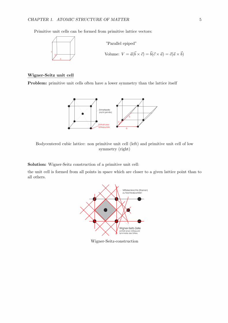
Wigner-Seitz unit cell
Problem: primitive unit cells often have a lower symmetry than the lattice itself
Bodycentered cubic lattice: non primitive unit cell (left) and primitive unit cell of lowsymmetry (right)
Solution: Wigner-Seitz construction of a primitive unit cell:
the unit cell is formed from all points in space which are closer to a given lattice point than toall others.
Wigner-Seitz-construction
CHAPTER 1. ATOMIC STRUCTURE OF MATTER 6
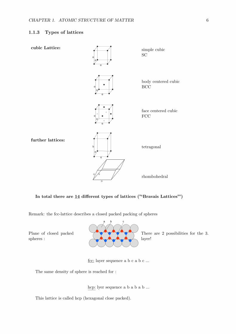
1.1.3 Types of lattices
cubic Lattice:
a
aa
simple cubicSC
a
a
a
body centered cubicBCC
a
aa
face centered cubicFCC
further lattices:
a
a
b tetragonal
rhombohedral
In total there are 14 different types of lattices (”‘Bravais Lattices”’)
Remark: the fcc-lattice describes a closed packed packing of spheres
Plane of closed packedspheres :
b ca
There are 2 possibilities for the 3.layer!
fcc: layer sequence a b c a b c ...
The same density of sphere is reached for :
hcp: lyer sequence a b a b a b ...
This lattice is called hcp (hexagonal close packed).

CHAPTER 1. ATOMIC STRUCTURE OF MATTER 7
fcc hcp
1.1.4 Examples
sc (single atom basis)
Po
Po
sc (two atom bases) Cs
Cl
CsCl,... BeCu, AlNi, CuZn (brass)
fcc (single atom basis) Cu, Ag, Ni,... Ar,Kr
fcc (two atom basis)
Cl Na
NaCl, KBr, MgO, PbS
fcc (two atom basis) Tetrahedral lattice with identical atoms: Si, Gewith different atoms: SnS, SiC, GaAs, CdS, AgI(
”zincblende structure“; structure of practically all semiconductors!)
bcc (single atom basis) Na, K, Fe, Mb
hcp (single atom basis) Be, Mg, Zn, Co
CHAPTER 1. ATOMIC STRUCTURE OF MATTER 8
1.1.5 Structure determinatin of Crystals
Diffraction of waves
A light wave is a electromagnetic field
E(x) = E0 cos(kx)
It is λ = 2πk or k = 2π
λ (k: wave number (or vector), unit [cm−1]).
- 1
0
1
2π/ k
E
xπ/ k
λ
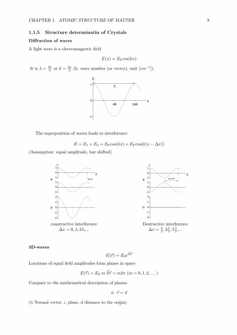
The superposition of waves leads to interference:
E = E1 + E2 = E0 cos(kx) + E0 cos(k(x−∆x))
(Assumption: equal amplitude, but shifted)
- 2- 1012
- 101
- 101
=
+
E
x∆ x = 0
constructive interference∆x = 0, λ, 2λ,...
- 2- 1012
- 101
- 101
=
+
E
x∆ x = λ / 2
Destructive interference∆x = λ
2 , 3λ2 , 5
λ2 ,...
3D-waves
E(~r) = E0ei~k~r
Locations of equal field amplitudes form planes in space
E(~r) = E0 ⇔ ~k~r = m2π (m = 0, 1, 2, . . . )
Compare to the mathematical description of planes:
n · ~r = d
(n Normal vector ⊥ plane, d distance to the origin)

CHAPTER 1. ATOMIC STRUCTURE OF MATTER 9
Normalization of ~k:~k
|~k|~r = m
2π
|~k|
The equation for the location of points of maximum amplitude describes planes Ebenen ⊥ ~kwith interplanar distance 2π
|~k|
x
y
kr
kπλ 2
=
Remark: Complex functions like ei~k~r in classical physics are mathematical constructions to
facilitate calculations; only the real part Re(ei~k~r) = cos(~k~r) of the functions count. In quantum
mechanics the imaginary part has the same significance as the real part!
1.1.6 Structure determination by x-ray diffraction
Bragg diffraction
Constructive/destructive interference depend-ing on phase shift.
Genauer: Path length difference between the partial beams:2δ = 2d cos(α)
Constructive interference if 2δ = nλ, n = 1, 2, 3, . . .
⇒ 2d cos(α) = nλ
cos(α) =nλ
2dBragg condition
CHAPTER 1. ATOMIC STRUCTURE OF MATTER 10
Because cos(α) ≤ 1 it follows that nλ2d ≤ 1 and therefore:
⇒ λ ≤ 2d
n
Only for small λ there are one (or more) possible angles!
Particle waves
Atoms, electrons and neutrons also form waves with wavelength
λ =h
pde-Broglie
p is the momentum of the particle, h = 6, 6262 · 10−34 Js is the Planck constant.
For typical distances between planes of d ∼ 2A one needs particles of the following energies fordiffraction epxeriments
Teilchen λ p E
Photon 12400 eV (x-rays!)
Elektron 1 A 6,6 · 10−24 kg ms 300 eV
Neutron 0,08 eV (= 630 K)
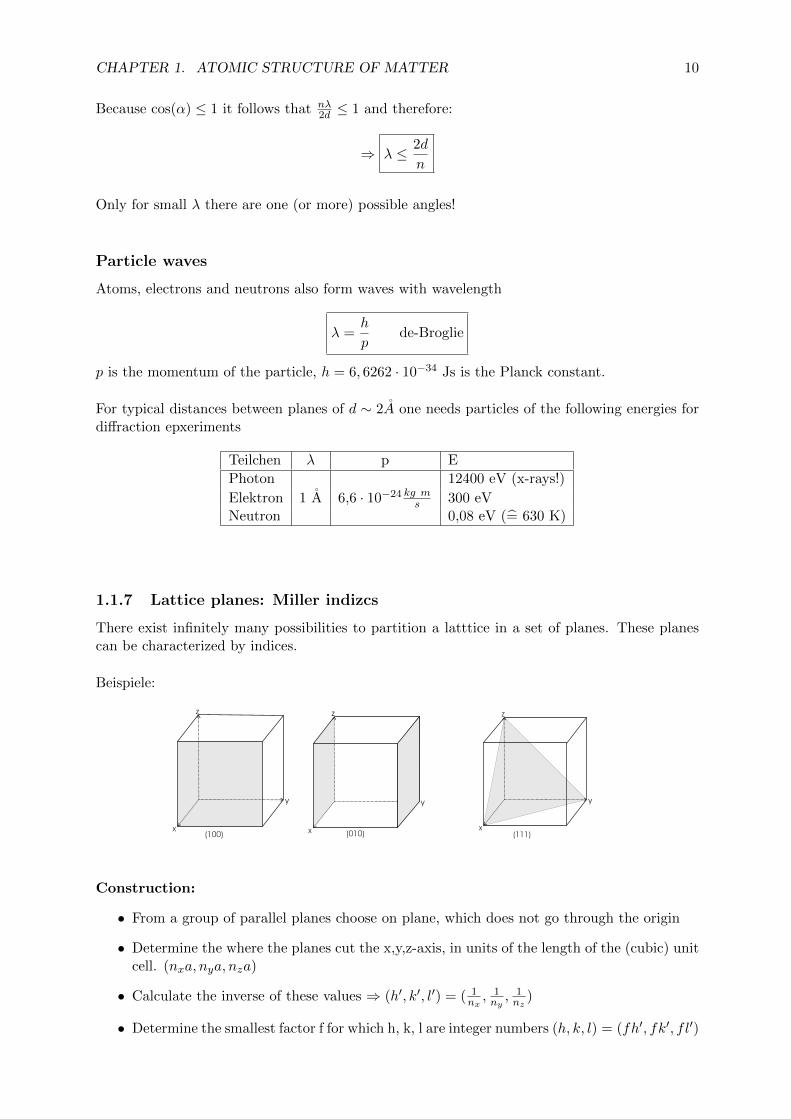
1.1.7 Lattice planes: Miller indizcs
There exist infinitely many possibilities to partition a latttice in a set of planes. These planescan be characterized by indices.
Beispiele:
Construction:
• From a group of parallel planes choose on plane, which does not go through the origin
• Determine the where the planes cut the x,y,z-axis, in units of the length of the (cubic) unitcell. (nxa, nya, nza)
• Calculate the inverse of these values ⇒ (h′, k′, l′) = ( 1nx, 1ny, 1nz
)
• Determine the smallest factor f for which h, k, l are integer numbers (h, k, l) = (fh′, fk′, f l′)

CHAPTER 1. ATOMIC STRUCTURE OF MATTER 11
Examples
sc
Axes intercepts :x = 2a, y = a, z =∞⇒ (h′, k′, l′) = (1
2 , 1, 0)⇒ f = 2⇒ (h, k, l) = (1, 2, 0)
(this was not the plane closest tothe origin, nevertheless the result wascorrect)
bcc
Axes intercepts:x =∞, y = 1
2a, z =∞⇒ (h′, k′, l′) = (0, 2, 0) = (h, k, l)
Remark
• Negative numbers are written as h: (1, 0, 1)
• h, k, l denominates all crystallographical identical planes; h ≥ k ≥ l
• 〈h, k, l〉 denominates the direction perpendicular to the plane
Properties of the Miller indices in cubic lattices
1. The position vector(hkl
)is perpendicular to the plane (hkl)
2. The distance d the planes is :
d =a√
h2 + k2 + l2
The larger the indices, the smaller the distance!
Consequences for the diffraction condition
Ablenkwinkelθ
α
Insertion of d into the Bragg condition: cosα = nλ2a
√h2 + k2 + l2
The deflection angle then becomes Θ = 180 − 2α
Θ = 2 arcsin(nλ
2a
√h2 + k2 + l2)
Small indices lead to small deflection angles!

CHAPTER 1. ATOMIC STRUCTURE OF MATTER 12
1.1.8 Diffraction on a 3D-crystal
Reminder: Fourier transformation
F(k) =1√2π
∞∫−∞
f(x)e−ikxdx
︸ ︷︷ ︸scalarproduct!
Spectral analysis
invers: f(x) =1√2π
∞∫−∞
F (k)eikxdk Fourier synthesis
3D: F (~k) =1
(√
2π)3
∫f(~r)e−i
~k~rd~r
f(~r) =1
(√
2π)3
∫F (~k)ei
~k~rd~k
Fourier synthesis of crystal lattices
f(x) =
∞∫−∞
F (k)eikxdk =∑j
cjeikjx
Illustration:

CHAPTER 1. ATOMIC STRUCTURE OF MATTER 13
k-space
F(k)
F(k)
F(k)
F(k)
f(x)
f(x)
f(x)
f(x)
x
x
x
x
k
k
k
k
k0-k0
2k0-2k0
3k0-3k0
k0
+
+
=0
2k
a π=
xkee xikxik
0cos2
00 =+ −
xkee xkixki
0
22
2cos2
00 =+ −
xkee xkixki
0
33
3cos2
00 =+ −
F(k)
. . . .
k
x
ak0
direct space
lattice in k-space:∑
m δ(k −m2πa ) lattice in direct space:
∑n δ(xi − na)
The Fourier transform of a sc-lattice with lattice constant a is a sc-lattice in k-space with constant2πa (”reciprocal” lattice)
Formal:1
(√
2π)3
∫ ∑i
δ(~r − ~ri)︸ ︷︷ ︸direktes Lattice
e−i~k~r =
∑j
δ(~k − ~Gj)︸ ︷︷ ︸reciprocal lattice
3D-diffraction
The amplitude of the wave at lattice point ~ri is
A = A0ei~k(~ri−~r0) | A0 bei ~r0
The amplitude in the detector plane then is (γ is the ”‘scattering efficiency”’):
A′ = γA0ei~k(~ri−~r0)ei
~k′(~r0′−~ri)
= γA0ei(~k−~k′)~riei(
~k′ ~r0′−~k ~r0)

CHAPTER 1. ATOMIC STRUCTURE OF MATTER 14
Gitter
Punkt inQuellebene
einlaufende Welle auslaufende Welle
Punkt inDetektorebene
λ
kr
'kr
'0rr0rr
irr
Summed over all lattice points and squared:
I(~k,~k′) = |A|2 = const. · |∑i
ei(~k−~k′)~ri |2
= const. · |∫ ∑
i
δ(~r − ~ri)ei(~k−~k′)~rd~r|2 |∆~k = ~k′ − ~k
= const. · |∫ ∑
i
δ(~r − ~ri)e−i∆~k~rd~r︸ ︷︷ ︸
Fouriertransf. des dir. Lattices
|2
It follows that I(∆~k) ∝ |∑
j δ(∆~k − ~Gj)|2
The scattering intensity therefore is not zero if
∆~k = ~G
general diffraction condition
The diffraction of a wave with wave vector ~k into the direction ~k′ only occurs if ∆~k = ~k′−~kis a vector of the reciprocal lattice!
1.1.9 Calculation of the reciprocal lattice
Formally: for a given lattice with primitive lattice vectors ~a1, ~a2, ~a3 one can calculate primitivelattice vectors of the reciprocal lattice ~b1, ~b2, ~b3 from the direct lattice ones:
~G = u1~b1 + u2
~b2 + u3~b3 (ui = 0, 1, 2, . . . )
For these it holds that:
~b1 = 2π~a2 × ~a3
~a1( ~a2 × ~a3), ~b2 = 2π
~a3 × ~a1
~a1( ~a2 × ~a3), ~b3 = 2π
~a1 × ~a2
~a1( ~a2 × ~a3)
Definition of primitiven lattice vectors of the reciprocal lattice
Properties
• for all~G of the reciprocal lattice it holds that ei~G~rj = 1 ∀~rj (lattice points of the direct
lattice)
• thus each ~G describes a set of planes interplanar distance
d = m2π
|~G|m = 1, 2, 3, . . .
and noraml vectorn =~G| ~G|

CHAPTER 1. ATOMIC STRUCTURE OF MATTER 15
• cubc lattices: the planes (h,k,l) (Miller indices) are described by ~G = n2πa
(hkl
);
the interplanar distance is d = n 2π| ~G|
= mn
a√h2+k2+l2
(m = n)
1.1.10 Examples
sc-Lattice
Lattice vectors: ~a1 = a(
100
), ~a2 = a
(010
), ~a3 = a
(001
)Volume unit cell: ~a1 · ( ~a2 × ~a3) = a3
Reziprocal lattice vectors: ~b1 = 2π ~a2× ~a3VEZ
= 2πa3
(100
)a2 = 2π
a
(100
)~b2 = 2π
a
(010
), ~b3 = 2π
a
(001
)
2p a
b2
b1
b3
sc-Lattice
bcc-lattice
Lattice vectors: ~a1 = a(
100
), ~a2 = a
(010
), ~a3 = a
( 121212
)VEZ = 1
2a3
Reciprocal lattice vectors: ~b1 = 2πa
(10−1
), ~b2 = 2π
a
(01−1
), ~b3 = 2π
a
(002
)linear combination: ~b1 + ~b3 = 2π
a
(101
), ~b2 + ~b3 = 2π
a
(011
)
b+11 b3 b+2 b3
b3
4p a fcc lattice!
fcc lattice
Lattice vectors: ~a1 = a( 1
2012
), ~a2 = a
( 01212
), ~a3 = a
(001
)VEZ = 1
4a3
~b1 = 2πa
(200
), ~b2 = 2π
a
(020
), ~b3 = 2π
a
(−1−11
)Linear combination: ~b1 + ~b2 + ~b3 = 2π
a
(111
)

CHAPTER 1. ATOMIC STRUCTURE OF MATTER 16
b+11 b3 b+2 b3
b3
4p a bcc-Lattice!
The reciprocal lattice of a sc-lattice (with edge length a) is a sc-lattice with edge length 2πa ;
that of a bcc- or fcc-lattice is a fcc- or bcc-lattice with edge length 4πa
⇒ there are fewer lattice vectors than in the case of the sc-lattice!
1.1.11 Structure factor
Diffraction from a lattice with basis
Exp.: simple cubic lattice with bBasis(
000
)a and
( 121212
)a = ~c
The diffraction amplitude here is:
A′ =
∫ ∑i
(δ(~r − ~ri) + δ(~r − ~ri − ~c)) · e−i∆~k~rd~r
=
∫ ∑i
δ(~r − ~ri)e−i∆~k~rd~r +
∫ ∑i
δ(~r − ~ri − ~c)e−i∆~k~rd~r ~r′ = ~r − ~c
=∑n
δ(∆~k − ~Gn) +
∫ ∑i
δ(~r′ − ~ri)e−i∆~k(~r′+~c)d~r′
=∑n
δ(∆~k − ~Gn) + e−i∆~k~c
∫ ∑i
δ(~r′ − ~ri)e−i∆~k~r′d~r′
= (1 + e−i∆~k~c)︸ ︷︷ ︸
structure factor for bcc-lattice
∑n
δ(∆~k − ~G)︸ ︷︷ ︸reciprocal lattice of the sc-lattice
6= 0 for ∆~k = ~G and ∆~k~c 6= (2n+ 1)π
This means all reciprocal lattice vector of the sc-lattice vanish for which
∆~k · ~c = ~G · ~c = (2n+ 1)π
2π
a
(hkl
)·( 1
21212
)a = (2n+ 1)π
π(h+ k + l) = (2n+ 1)π
h+ k + l = (2n+ 1)
CHAPTER 1. ATOMIC STRUCTURE OF MATTER 17
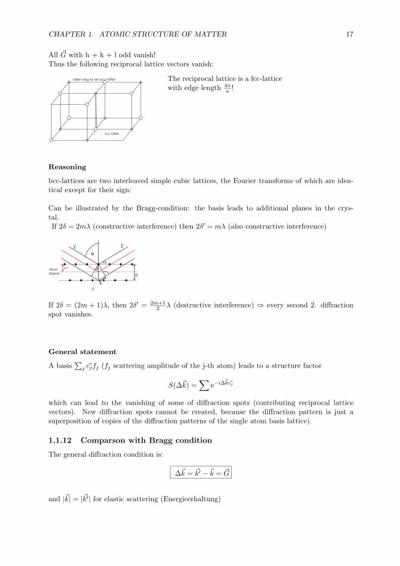
All ~G with h + k + l odd vanish!Thus the following reciprocal lattice vectors vanish:
The reciprocal lattice is a fcc-latticewith edge length 4π
a !
Reasoning
bcc-lattices are two interleaved simple cubic lattices, the Fourier transforms of which are iden-tical except for their sign:
Can be illustrated by the Bragg-condition: the basis leads to additional planes in the crys-tal.If 2δ = 2mλ (constructive interference) then 2δ′ = mλ (also constructive interference)
If 2δ = (2m + 1)λ, then 2δ′ = 2m+12 λ (destructive interference) ⇒ every second 2. diffraction
spot vanishes.
General statement
A basis∑
j ~cjfj (fj scattering amplitude of the j-th atom) leads to a structure factor
S(∆~k) =∑
e−i∆~k~cj
which can lead to the vanishing of some of diffraction spots (contributing reciprocal latticevectors). New diffraction spots cannot be created, because the diffraction pattern is just asuperposition of copies of the diffraction patterns of the single atom basis lattice).
1.1.12 Comparson with Bragg condition
The general diffraction condition is:
∆~k = ~k′ − ~k = ~G
and |~k| = |~k′| for elastic scattering (Energieerhaltung)

CHAPTER 1. ATOMIC STRUCTURE OF MATTER 18
It holds that:
~G~k′ = |~G||~k′|cos(α)
~G~k = −|~G||~k|cos(α)
From the diffraction condition it follows that
~k − ~k′ = ~G | · ~G~k′ ~G− ~k ~G = |~G|2
With ~k′ ~G = −~k ~G this becomes
2~k′ ~G = |~G|2
(general diffraction condition for elastic scattering)
Inserting this into the equations above gives
2|~k||~G|cos(α) = |~G|2
cos(α) =|~G|2|~k|
With wave number |~k| = |2π|λ and interplanar distannce d = 2π
| ~G|it follows that
cos(α) =m2π
2d
λ
2π
cos(α) = mλ
2dBragg Bedingung!
1.1.13 Ewald construction
Graphical solution of the general diffraction condition ∆~k = ~G und |~k′| = |~k|:
• In the reciprocal lattice the wave vector ~k of the incoming wave is drawn such that its tipis located on a lattice point.
• A circle (sphere) is drawn around the base point of the vector with a radius of |~k|.
• If the sphere touches a lattice point, a possible allowed final wave vector ~k′ is given by thevector running from the base of ~k to this point.
The circular line has zero area, so the probability for a lattice point to lie exactly on the lineis usually zero! So normally there is no diffraction at all! In order to observe diffraction one hasto vary some parameters. There are two standard methods to do this:
Laue diffraction
• oriented single crystal
• ”white” x-rays(continuous spectrum)
The radius of the Ewald sphere exhibits a continuous distribution -resulting diffraction spots therefore have different ”colors”.

CHAPTER 1. ATOMIC STRUCTURE OF MATTER 19
Kreis mit Radius |k|
kr
'kr
Gr
Debye-Scherrer diffraction
• monochromatic x-rays
• crystal powder (all orientations)
The lattice can have any orientation; the lattice points therefore describe spherical surfacesdiffraction rings
1.1.14 Atom form factor
The scattering intensity of an atom depends on the deflection angle and the wavelength. Forx-rays is is given by
f(∆~k) =∫
n(~r)e−i∆~k~r d~r
n(~r): elektron distribution in the atomf(∆~k): Fourier transformof the electron density (every electron scatters locally)
For spherical symmetry (n(~r) = n(r)) this becomes:
f(∆k) = 4π
∞∫0
n(r)sin(∆kr)
∆krr2 dr
f(∆k) decreases for large ∆k (large Miller indices)!
Summarizing, the resulting diffraction intensity is (crystal made of one element):
I(∆k) =∑~G
δ(∆~k − ~G)
︸ ︷︷ ︸rec. lattice︸ ︷︷ ︸
Fourier transform of the lattice
· S(∆~k)︸ ︷︷ ︸structure factor
· f(∆~k)︸ ︷︷ ︸atom form factor︸ ︷︷ ︸
Fourier transform of the basis
1.1.15 Einheitszelle des Reciprocaln Lattices
Like for the direct lattice one can form a primitive unit cell out of the primitive lattice vectors~b1, ~b2, ~b3 bilden.This cell usually does not have the symmetry of the lattice, so is is better to use a Wigner-Seitzconstruction.
Definition: the Wigner-Seitz cell of the reciprocal lattice is called 1. Brillouin zone

CHAPTER 1. ATOMIC STRUCTURE OF MATTER 20
The construction of the unit cell is completely analogous to the construction of the Wigner-Seitzcell in direct space: one draws bisecting planes on all connection lines between a given point andall other points of the lattice. The 1. Brillouin zone is the innermost of volumes defined by theintersecting planes. Further zones (2. Brillouinz one etc.) can be defined by counting the numberof planes (zone boundaries) which have to be traversed to get to a region (more specifally: the 1.BZ is the region formed from all points for which the given point is the closest lattice point; the 2.BZ is formed from points, for which the given point is the second closest lattice point and so on).
Mittelsenkrechte zu Nachbarpunkten
1. BZ
2. BZ
3. BZ
Important: all Brillouin zones have the same volume; the higher zone can be transformed intothe 1. BZ by translation of their different regions by reciprocal lattice vectors!
Reminder: diffraction
Ortsraum k-Raum
points in k-space describe plane waves in di-rect space
Reciprocal lattice vectors
~G0 describes a plane wave with a wavelengthequal to the interplanar distance d in thecrystaln ~G0 describe waves with wavelength d
n
The set of planes is annotated by ~G0 (short-est vector in this direction)
Diffraction:hapes in direct space: k-sspace
CHAPTER 1. ATOMIC STRUCTURE OF MATTER 21
diffraction occurs at all atoms of the lattice. ~k → ~k′ is only possible, if the atoms form planeswhich
1. are perpendicular to ~k′ − ~k (specular reflection)
2. have a distance d = n2
λcosα (Bragg condition)
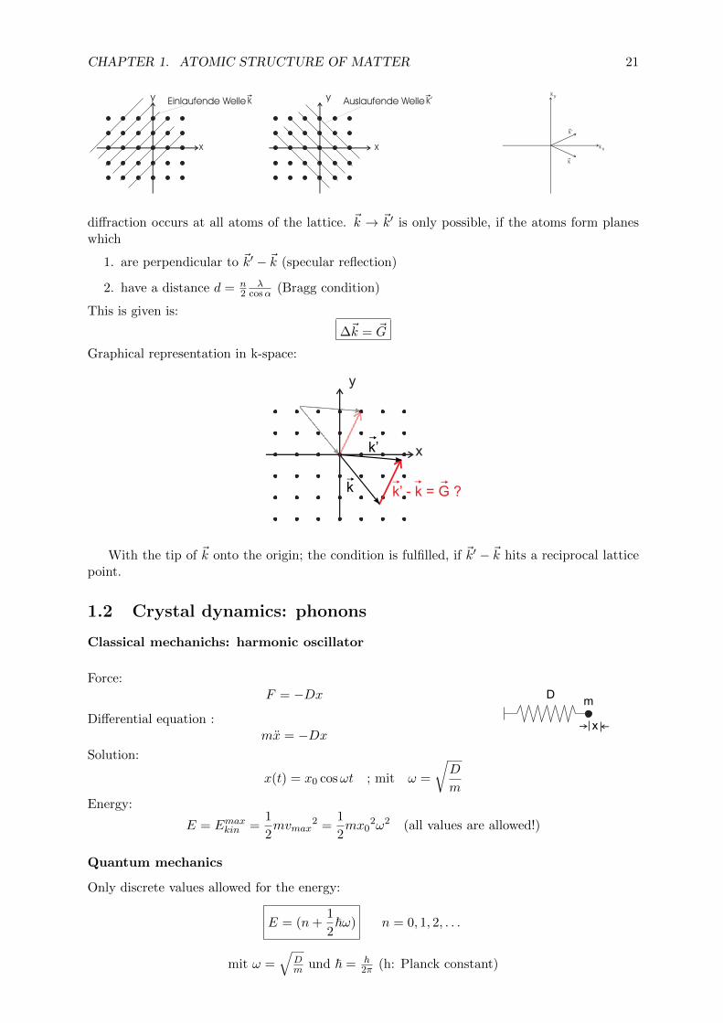
This is given is:
∆~k = ~G
Graphical representation in k-space:
y
x
k
k’
k’ - k = G ?
With the tip of ~k onto the origin; the condition is fulfilled, if ~k′ − ~k hits a reciprocal latticepoint.
1.2 Crystal dynamics: phonons
Classical mechanichs: harmonic oscillator
Force:F = −Dx
Differential equation :mx = −Dx
Dm
x
Solution:
x(t) = x0 cosωt ; mit ω =
√D
m
Energy:
E = Emaxkin =1
2mvmax
2 =1
2mx0
2ω2 (all values are allowed!)
Quantum mechanics
Only discrete values allowed for the energy:
E = (n+1
2~ω) n = 0, 1, 2, . . .
mit ω =√
Dm und ~ = h
2π (h: Planck constant)

CHAPTER 1. ATOMIC STRUCTURE OF MATTER 22
Holds for all periodic processes (oscillations)!
1.2.1 Linear chain (1D-model for solid matter)
Chain of masses and springs (infinitely long)
u
a
Force onto the n-te mass:
F = D((un+1 − un)− (un − un−1))
⇒ mun = D((un+1 − un)− (un − un−1))
Ansatz:un(t) = u0eiknae−iωt
Insertion:
m(−ω2)u0eiknae−iωt = Du0(eik(n+1)a + eik(n−1)a − 2eikna)e−iωt
−mω2 = D(eika + e−ika︸ ︷︷ ︸2 cos ka
−2)
ω2 =2D
m(1− cos ka)
and thus:
ω =
√2D
m(1− cos ka)
This is the so-called dispersion relation of phonons.
mD4
3π/a-3π/a -2π/a -π/a 0 2π/a
ω (k)
kπ/a
1. BrillouinzonereziprokeGitterpunkte
Dispersionsbeziehungder linearen Kette
Because of√
1− cosα =√
2 sin2 α2 =√
2 · | sin α2 | one obtains a sine function.
Significance of the Briillouin zone: only values of k within the 1. BZ describe different vibrationalmodes.A vibrational mode described by any vector in k-space can be also described by a vector fromthe 1. BZ (or any other chosen BZ).
Wave form for different wave vectors

CHAPTER 1. ATOMIC STRUCTURE OF MATTER 23
ak
3π
=
0=k
ak π=
un
un
un
Ga
k
+=
=
0
2π
un
a
For k = 2π/a one gets the same motion of the atom as for k = 0, because the wave functiononly gets evlauated at the locations of the atoms!
Formally:
for ~k = ~k1.BZ + ~G it holds that:
ei~k~ri = ei(
~k1.BZ+ ~G)~rj = ei~k1.BZ ~rj ei
~G~ri︸︷︷︸1
= ei~k1.BZ ~rj
3D-Kristall
Longitudinal and transversal modes
Dispersion:
logitudinalω
k
L
Ttransversal(2 Moden)
1.2.2 Measurement of the phonon dispersion
Possible by inelastic scattering of photons, electrons, neutrons, or even He atoms.Often used: neutrons

CHAPTER 1. ATOMIC STRUCTURE OF MATTER 24
MOmentum: p =h
λ=h · 2π2π · λ
= ~k
Kinetic energy: Ekin =1
2mv2 =
p2
2m=
~2k2
2m
”‘Normal”’ diffraction condition
∆~k = ~k′ − ~k = ~G (”‘Conservation of momentum”’)
|~k′| = |~k| (”‘Conservation of energy”’)
Inelastic scattering
Creation of elimination of a phonon with wave vector~q and energy ~ω(~q)For a neutron one has:
energy: E′kin = Ekin ± ~ω~q (+ for phonon elimination)
more precisely:~2
2m|~k′|2 =
~2
2m|~k|2 ± ~ω(~q)
Impuls: ~p′ = ~p+ ~~G± ~~q
1.2.3 Lattice with a basis
In the case of more than one atom per lattice point there are more vibrational modes per ~k.
zwei Atomsorten
l l
Low frequency (“acoustic”) High frequency (“optical”)
Dispersion
LATA
k
LOTO optischer Zweig
akustischer Zweig
w(k)
A typical value for the frequency of the ”‘optical”’ branch is ν = 1013 Hz. This corresponds toa wavelength of light of λ = 30µm (far infrared). ”‘Optical”’ therefore does not mean ”‘visible”’ !
1.2.4 Velocity of sound
vPh: phase velocity (motion of the location of a given phase)vGr: group velocity

CHAPTER 1. ATOMIC STRUCTURE OF MATTER 25
Relation to the dispersion ω(k):
vPh =ω(k)
k
vGr =dω(k)
dk
Dispersion relation for a lattice with a monoatomic basis
ω2(k) =2D
m(1− cos(ka))
for small k can be written as
ω2(k) =2D
m(1− (1− (ka)2
2)) =
D
m(ka)2
⇒ ω(k) ≈√D
mka
It follows that:
vPh =
√D
ma ; vGr =
√D
ma
The velocity of sound (both phase and group velocity!) is independent of k for small k!
1.2.5 Interaction with phonons
Phonons have energy (~ωPh) and wave number (kq = 2π/λ) but no momentum ! (Most easilyseen for transversal modes; there is no motion of masses in the propagation direction.So what is the reason for the ”conservation of momentum” ~k′ = ~k + ~G+ ~q ?
1. Explanation: lattice deformationA phonon creates a periodic deformation of the lattice
this ”grating” can cause Bragg reflection⇒ ~k′ = ~k + ~q (the general dffraction condition holds for all kind ofperiodic structures)
Why is this scattering inelastic?The periodic structure (the deformation) is moving! (classically: refelction from a movingmirror)

CHAPTER 1. ATOMIC STRUCTURE OF MATTER 26
Transformation into the frame of reference of the phonon (themoving deformation) (wave lengths stay constant, frequencies ex-perience the Doppler effect).
incoming wave:
E(~k) = ~ω(~k) = ~ω(~k)− ~~k~v
outgoing wave:
E(~k′) = ~ω(~k′) = ~ω(~k′)− ~~k′~v
In the moving frame of reference the scattering is eleastic, so
ω(~k) = ω(~k′)
Consequently in the lab frame
E′ − E = ~ω(~k′)− ~ω(~k)
= ~(~k′ − ~k)~v
It holds that ~k′ − ~k = ~qPh and furthermore
vPh =ωPhq
or ~vPh =ωPh|~q|
~q
|~q|It follows that :
E′ − E = ~~qPhωPh|~q|
~q
|~q|= ~ω
The energy of the scattered photon is changed by the energy of the phonon!
2. Illustrative explanation: “side band modulation”A temporal periodic modulation of a wave creates additional frequency components:
cos(ω1t)cos(ω2t) = cos((ω1 + ω2)t) + cos((ω1 − ω2)t)
The Fourier transform of such a wave would than be (in the case of weak modulation):
This holds for any wave:the interaction with the lattice deformationmodulates the wave.
ei~k~r · eiωt︸ ︷︷ ︸
incoming wave
· ei~q~r · e±iωPht︸ ︷︷ ︸phonon
= ei(~k+~q)~r︸ ︷︷ ︸
side band in space︸ ︷︷ ︸“momentumconservation′′
· ei(ω±ωPh)t︸ ︷︷ ︸side band in time︸ ︷︷ ︸
“energyconservation′′

CHAPTER 1. ATOMIC STRUCTURE OF MATTER 27
Spatial modulation : ~k → ~k + ~q conservation of the wave vectorTemporal modulation: ω → ω ± ωPh conservation of energy
The inelastic diffraction of a wave by the crystal corresponds to the collision of a particle(the photon) and a different particle (the phonon) with momentum ~~q and energy ~ω(although in fact the particle gets created or eliminated). This is true for all wave-likeexcitations.
1.2.6 Debye-Waller factor
Structure factor with moving atoms (summation over the basis of the crystal):
S(∆~k) = S(~G) =∑j
fje−i ~G(~rj+ ~uj(t))
fj : form factors of the basis atoms. Since all atoms move differently, one would have to averagethe structure factor over the whole crystal.Assumption: averaging over time is equal to averaging over the crystal.
S(~G) =∑j
fje−i ~G~rj 〈e−i ~G ~uj 〉t
For small displacements of the atoms one can make a series expansion of the exponential function:
〈e−i ~G~u(t)〉t = limτ→∞
1
τ
τ∫0
e−i~G~u(t)dt
= 〈1− i ~G~u(t)− 1
2(~G~u(t))2 + ...〉
= 1− 1
2〈(~G~u(t))2〉 | ~G~u = |~G||~u| · cos(ϑ)
= 1− 1
2~G2〈~u2〉 〈cos2 ϑ〉ϑ︸ ︷︷ ︸
13
= 1− 1
6~G2〈~u2〉 ' e−
16~G2〈~u2〉
The scattering intensity (squared absolute value of the amplitude) is then:
I = |S(~G)|2 = |S0|2︸︷︷︸structur factorwithout phonons
e−13~G2<~u2>︸ ︷︷ ︸
Debye-Waller factor
Harmonic approximation: the atoms are considered as independent three-dimensional
harmonic oscillators (with frequency ω =√
Dm)
Potntial energy in thermal equilibrium:
Epot =1
2D〈~u2〉 =
D
2(〈x2〉+ 〈y2〉+ 〈z2〉)
=3
2kBT

CHAPTER 1. ATOMIC STRUCTURE OF MATTER 28
It follows that
〈~u2〉 =3kBT
D=
3kBT
mω2
I(~G) = I0e−kBT
~G2
mω2 fur kBT ~ω
(m: atom mass, ω typical oscillation frequency)
Low temperatures: energy of the harmonic oscillator:
Etot = (nx +1
2)~ω + (ny +
1
2)~ω + (ny +
1
2)~ω
→ 3
2~ω (fur T → 0K)
〈Epot〉 =1
2D〈u2〉 =
1
2Etot =
3
4~ω
⇒ 〈u2〉 =3
2
~ωmω2
The scattering intensity then becomes:
I(~G) = I0e−~~G2
2mω fur kBT ~ω
This I(~G) describes the scattering intensity at T=0K, which is reduced by phonon creation(phonon-elimination is not possible at T=0K, because there no thermally created phonons).The exponential term (the Debye-Waller factor) gives the probability of elastic scattering, thatis the probability, that no phonon is created.
Example with typical values:With |~G| = (0.1A)−1; ω = 2π · 1013s−1; m = 50 ∗ 1,67 · 10−27kg one gets
I(~G) = 0.9I0 fur T → 0K
So ≈ 90% of the particles (neutrons, photons) get elastically scattered; in 10% of the cases aphonon gets created.
This is quantum effect Classically a scattered particle would always excite some lattice vi-brations.(this effect is made us of in Moßbauer-spectroscopy: here photon emission/absorption occurswithout energy loss due to recoil)

CHAPTER 1. ATOMIC STRUCTURE OF MATTER 29
Summary scattering from crystals
Kristall
kr
E0
Energieverteilungder einlaufenden Welle
E0
E0 ωh±
Energiespektren
Beugungsintensität
elastischeBeugung
Gkrr
=Δ
inelastischeBeugung
Gkrr
≠Δ
nimmt ab mit T
nimmt zu mit T
1.3 Heat capacity
1.3.1 Classical thermodynamics
A crystal with N atoms has 6N degrees of freedom (3N of the kinetic energy and 3N of thepotentiaal energy)Ein Kristall mit N Atomen hat 6N Freiheitsgrade (3N der kinetischen Energieund 3N der potentiellen Energie).
Equipartition theorem: at temperature T every degree of freedom on average is excited with
an energy of 12kBT . (kB Boltzmann constant: 1,38 · 10−23 J
K )
⇒ thermal ebergy of a crystal with N atoms:
E = 6N1
2kBT = 3NkBT
The heat capacity CV = ddTE(T ) then is:
CV = 3NkB Dulong-Petit
Agrees well with experiment at high temperatures; at low temperatures the heat capacitiesof all materials vanish, in contrast to the Dulong-Petit law (CV → 0 fur T → 0)
1.3.2 Quantum mechanics: Einstein model
Assumption: enbery atom in the solid forms an independent harmonic oscillator with frequencyω (the same for all atoms)
The energy of a harmonic oscillator is
En = (n+1
2)~ω , n = 0, 1, 2, . . .
The probability for a thermally induced occupation of the n-th state is
Pn =e− EnkBT∑∞
n=0 e− EnkBT
=e− (n+1/2)~ω
kBT∑∞n=0 e
− (n+1/2)~ωkBT
=e− n ~ωkBT∑∞
n=0 e− n ~ωkBT

CHAPTER 1. ATOMIC STRUCTURE OF MATTER 30
For x < 1 this gives∞∑n=0
xn =1
1− x
and therefore:
Pn = e− n ~ωkBT
(1− e
− ~ωkBT
)The average excited state at temperature thus is
〈n〉 =
∞∑n=0
nPn =
(1− e
− ~ωkBT
) ∞∑n=0
ne− n ~ωkBT
With∞∑n=0
nxn =x
(x− 1)2
this becomes
〈n〉 =1
e~ωkBT − 1
The thermal energy of a solid made of N atoms (3N harmonic oscillators) is then
E = ~ω(1
2+ 〈n〉)3N = ~ω(
1
2+
1
e~ωkBT − 1
)3N
This gives a heat capacity of
CV =d
dTE =
d
dT
(~ω(
1
2+
1
e~ωkBT − 1
)3N
CV = 3NkB(~ωkBT
)2 e~ωkBT
(e~ωkBT − 1)2
Einstein Modell
Discussion:
For T →∞ one gets e~ωkBT → 1 + ~ω
kBTand thus
CV = 3NkB
(~ωkBT
)2
·1 + ~ω
kBT
( ~ωkBT
)2= 3NkB
For high temepraturres the heat capcity converges to the Dulong-Petit value!
For T → 0 one gets e~ωkBT 1 and thus
CV = 3NkB
(~ωkBT
)2
e− ~ωkBT
For low temperatures the heat capacity strongly drops and converges to zero!
One gest the following temperature dependence of the heat capacity:
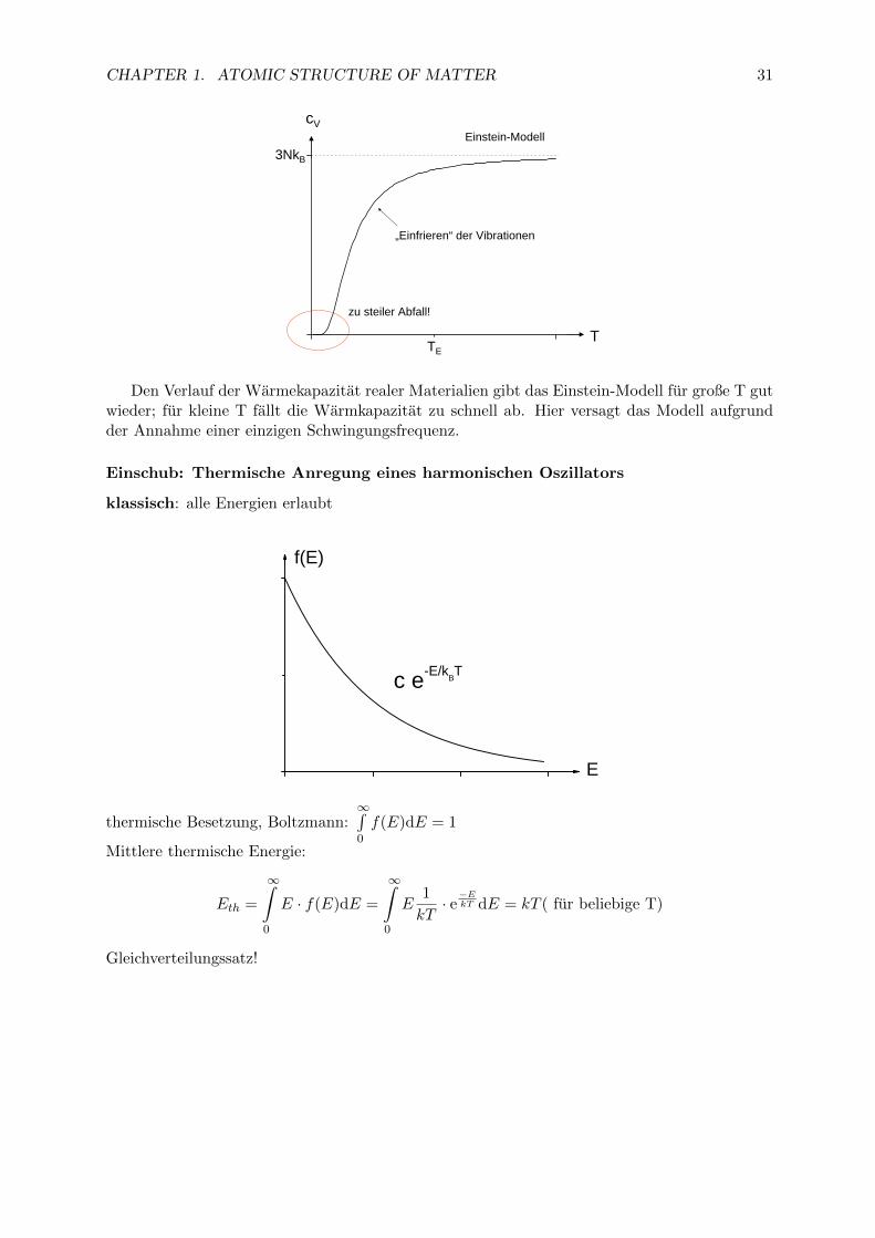
CHAPTER 1. ATOMIC STRUCTURE OF MATTER 31
cV
T
3NkB
zu steiler Abfall!
„Einfrieren“ der Vibrationen
TE
Einstein-Modell
Den Verlauf der Warmekapazitat realer Materialien gibt das Einstein-Modell fur große T gutwieder; fur kleine T fallt die Warmkapazitat zu schnell ab. Hier versagt das Modell aufgrundder Annahme einer einzigen Schwingungsfrequenz.
Einschub: Thermische Anregung eines harmonischen Oszillators
klassisch: alle Energien erlaubt
c e-E/kBT
f(E)
E
thermische Besetzung, Boltzmann:∞∫0
f(E)dE = 1
Mittlere thermische Energie:
Eth =
∞∫0
E · f(E)dE =
∞∫0
E1
kT· e−EkT dE = kT ( fur beliebige T)
Gleichverteilungssatz!

CHAPTER 1. ATOMIC STRUCTURE OF MATTER 32
T3T2
E/kBT e-E/kBT
E f(E)
E
T1
quantenmechanisch: diskrete Energien∑n
f(En) = 1 mitf(En) = (1− e−~ωkT )(e−n
~ωkT )
Mittlere thermische Energie :
Eth =∑n
Enf(En) =∑n
n~ω(1− e−~ωkT )e−n
~ωkT =
~ωe
~ωkT − 1
3hω2hω
T3
T2
E(1-e-hω/kBT) e-E/kBT
E f(E)
E
T1
hωT3 : Summe ≈ Integral Eth → kTT1 : Summe Integral Eth → 0
diskrete Anregungen frieren aus bei T → 0(System besetzt fast nur den untersten Zustand)
1.3.3 Quantenmechanik: Debye-Modell
Schwingungen haben unterschiedliche Frequenzen (Dispersion!)⇒ Einfrieren der Schwingungen ist uber einen breiten Temperaturbereich ”‘verschmiert”’.
Def.: Zustandsdichte D(ω): Anzahl der Schwingungen im Frequenzintervall [ω, ω + δω]

CHAPTER 1. ATOMIC STRUCTURE OF MATTER 33
Damit ist die thermische Energie:
E =
∞∫0
D(ω)~ω〈n(ω)〉Tdω
Berechnen von D(ω):
1. Berechnung der Zustandsdichte der Schwingungsmoden im k-Raum: ρ(~k)
2. Variablentransformation: D(ω) = ρ(k(ω)) dkdω
Zustandsdichte im k-Raum
Modell: 1D-Kristall (endlich lange Kette)
L
a
erlaubte Schwingungen (bei periodischen Randbedingungen)
L=λ ;L
k π2=
2L
=λL
k π4=;
a2=λa
k π=;
. . .
Fur einen endlichen Kristall sind die erlaubten Wellenvektoren gegeben durch:
k = nkmin = n2π
Lmit n=0,1,2,3 ..
kmax =π
a
Anzahl erlaubter k-Vektoren in der 1. Brillouinzone:
nk =∆k
kmin=
2πa
2πL
=L
a= NAtome Anzahl der Atome!
Debye: Zahlen von erlaubten k-Vektoren im k-Raum
endlicher 1D-Kristall
0aπ
aπ
−
Lπ2
1. Brillouinzone
erlaubte k-Werte
k
Anzahl:2πa2πL
= La = NAtome
CHAPTER 1. ATOMIC STRUCTURE OF MATTER 34
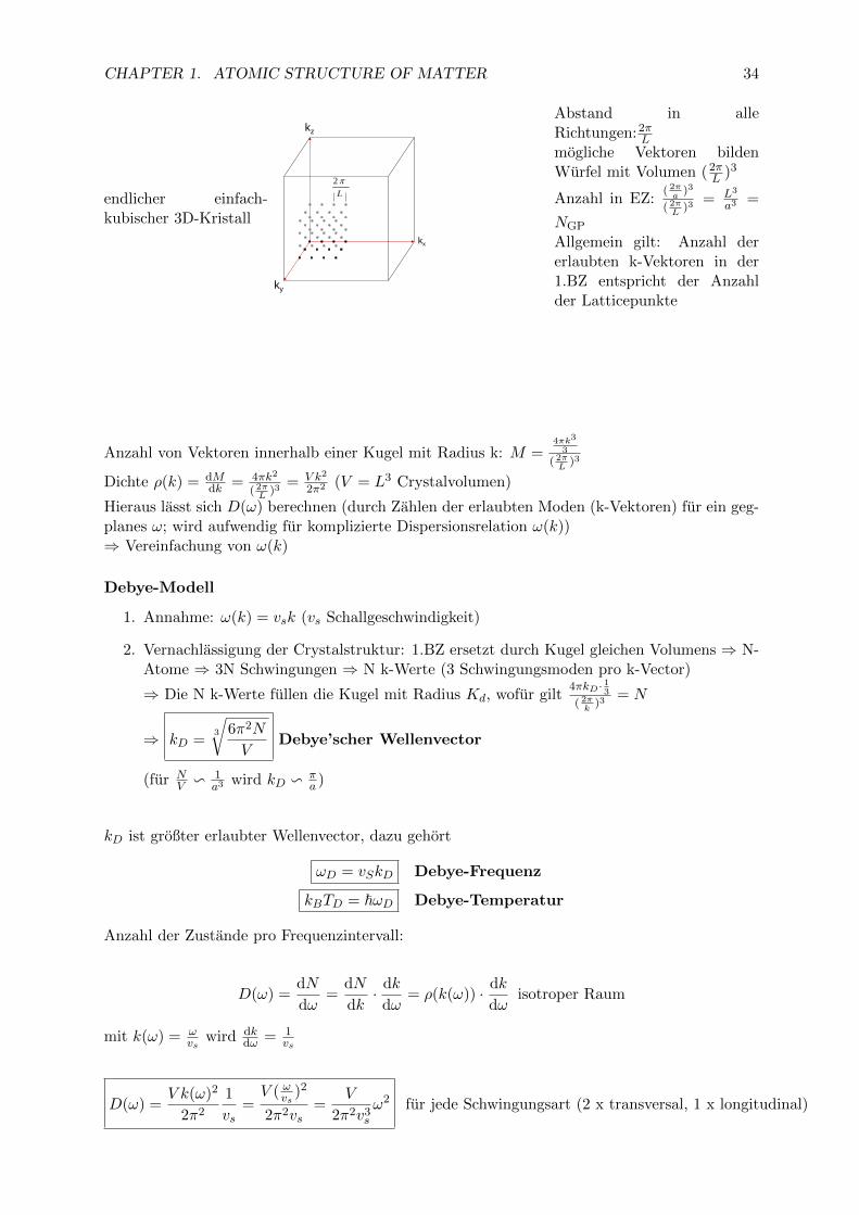
endlicher einfach-kubischer 3D-Kristall
kx
ky
kz
Lπ2
Abstand in alleRichtungen:2π
Lmogliche Vektoren bildenWurfel mit Volumen (2π
L )3
Anzahl in EZ:( 2πa
)3
( 2πL
)3 = L3
a3 =
NGP
Allgemein gilt: Anzahl dererlaubten k-Vektoren in der1.BZ entspricht der Anzahlder Latticepunkte
Anzahl von Vektoren innerhalb einer Kugel mit Radius k: M =4πk3
3
( 2πL
)3
Dichte ρ(k) = dMdk = 4πk2
( 2πL
)3 = V k2
2π2 (V = L3 Crystalvolumen)
Hieraus lasst sich D(ω) berechnen (durch Zahlen der erlaubten Moden (k-Vektoren) fur ein geg-planes ω; wird aufwendig fur komplizierte Dispersionsrelation ω(k))⇒ Vereinfachung von ω(k)
Debye-Modell
1. Annahme: ω(k) = vsk (vs Schallgeschwindigkeit)
2. Vernachlassigung der Crystalstruktur: 1.BZ ersetzt durch Kugel gleichen Volumens ⇒ N-Atome ⇒ 3N Schwingungen ⇒ N k-Werte (3 Schwingungsmoden pro k-Vector)
⇒ Die N k-Werte fullen die Kugel mit Radius Kd, wofur gilt4πkD· 13( 2πk
)3 = N
⇒ kD =3
√6π2N
VDebye’scher Wellenvector
(fur NV v 1
a3 wird kD v πa )
kD ist großter erlaubter Wellenvector, dazu gehort
ωD = vSkD Debye-Frequenz
kBTD = ~ωD Debye-Temperatur
Anzahl der Zustande pro Frequenzintervall:
D(ω) =dN
dω=
dN
dk· dk
dω= ρ(k(ω)) · dk
dωisotroper Raum
mit k(ω) = ωvs
wird dkdω = 1
vs
D(ω) =V k(ω)2
2π2
1
vs=V ( ωvs )2
2π2vs=
V
2π2v3s
ω2 fur jede Schwingungsart (2 x transversal, 1 x longitudinal)

CHAPTER 1. ATOMIC STRUCTURE OF MATTER 35
Thermische Energie des Crystals (fur eine Schwingungsart)
E =
∞∫0
D(ω) < n(ω) > ~ωdω
=
ωD∫0
V ω2
2π2v3s
· ~ωe
~ωkT − 1
dω
(Annahme: alle 3 Schwingungsarten habe gleiche Dispersion)
E =3V ~
2π2v3s
·ωD∫0
ω3
e~ωkT − 1
dω
=3V k4
BT4
2π2v3s~3
xD∫0
x
ex − 1dx wobei xD =
~ωDkT
=kBTDkT
=TDT
Es ist kBTD = ~ωD = ~vskD ⇒ TD = ~vskB
(6π2NV )
13 ⇒ V = 6π2N( ~vs
kBTD)3
Damit wird: E = 9NkBT (T
TD)3 ·
xD∫0
x3
ex − 1dx thermische Energie im Debye-Modell
Diskussion
fur hohe T (xD = TDT → 0) wird ex − 1 ≈ 1 + x− 1 = x
⇒xD∫0
x
ex − 1dx =
xD∫0
x2dx⇒ E = 3NkBT
fur tiefe Temperaturen (xD →∞) wird∞∫0
x3
ex−1dx = π4
15
E =9Nkπ4
15· T
4
TD⇒ CV =
dE
dT∼ T 3
Damit die Warmekapazitat des Festkorpers:fur hohe T: CV = 3NkBfur tiefe T: CV v T 3 Ubergang bei T = TD !

CHAPTER 1. ATOMIC STRUCTURE OF MATTER 36
Debye-Temperatur
TD
T
cV
3NkB
Debye-Modell
T3-Abhängigkeit!
Beispiele
mAt TD/KCu 63,5 343Au 197 165Pb 207 105Cs 133 38Al 27 428Si 28 645C(Diamant) 12 2230
je leichter das Atom und je harter dasMaterial ist, desto hoher ist TD (wegen
ω =√
DM )
Bemerkung: Spezifische Warmekapazitat (pro Volumen)
cv =1
VCV ⇒ cV (T →∞) =
3N
VkB = 3nkB
1.3.4 Warmeleitung durch Phononen
Warmeleitfahigkeit H wird definiert durch
Warmestrom j = −κdTdx
[κ] = [ω
mk]
Warmeleitung durch Phononen:Jedes Phonon ubertragt Energie ~ω ⇒ Warmeleitung
Genauer: Annahme:Freie Weglange lPh fur Phononen
Energiedichte: ub = cvTb (Phononendichte)
CHAPTER 1. ATOMIC STRUCTURE OF MATTER 37
Warmefluss: j = u · vs
Fluss durch Flache A: j = j→ − j← = uavs − ubvs = −cv∆Tvs⇒ j = −cvvs dTdx lPh
Fast richtig: in 3D muss man uber die Richtung der Phononen mitteln; bringt Faktor 13
⇒ j = −1
3cvvslPh
dT
dx
⇒ κ =1
3cvvslPh =
1
3cvv
2sτPh (τPh: Lebensdauer Phonon)
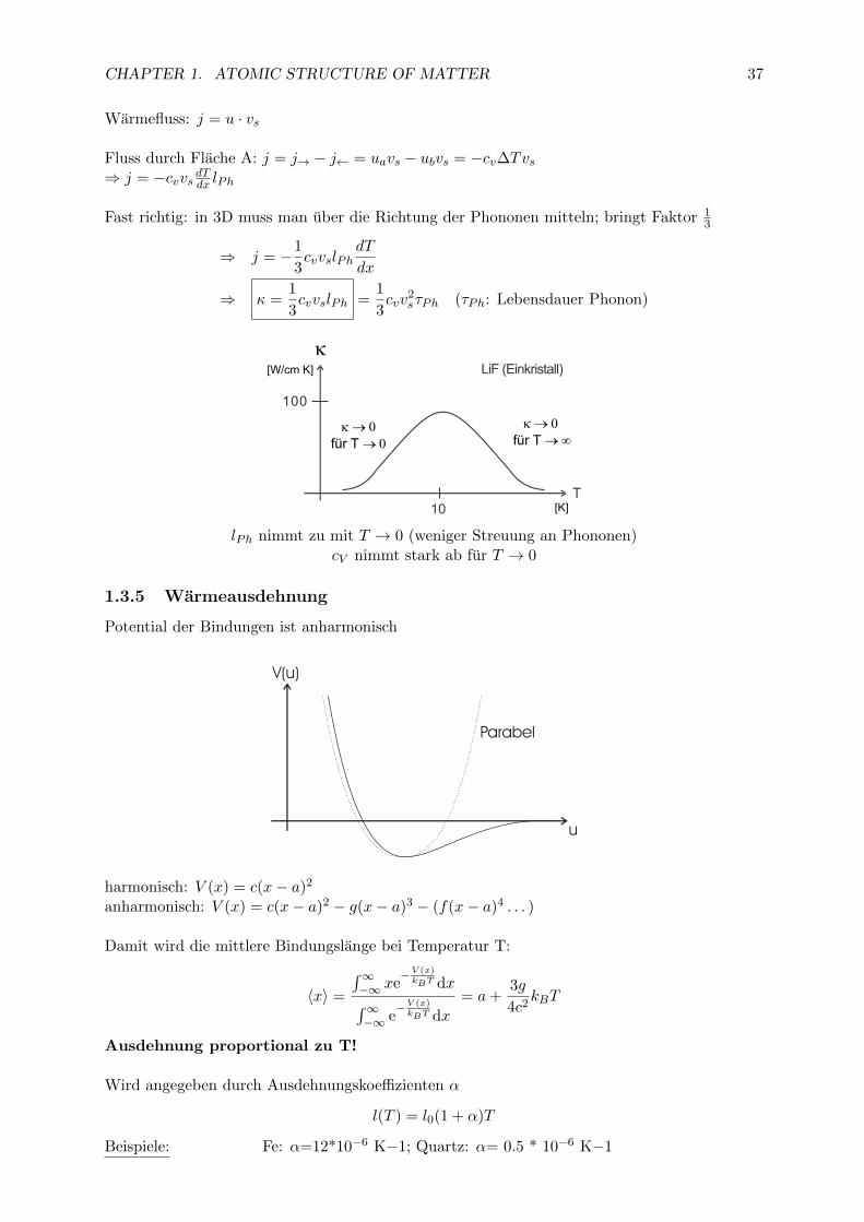
T10
100
LiF (Einkristall)k
[W/cm K]
[K]
k ® 0 für T ® ¥
k ® 0 für T ® 0
lPh nimmt zu mit T → 0 (weniger Streuung an Phononen)cV nimmt stark ab fur T → 0
1.3.5 Warmeausdehnung
Potential der Bindungen ist anharmonisch
harmonisch: V (x) = c(x− a)2
anharmonisch: V (x) = c(x− a)2 − g(x− a)3 − (f(x− a)4 . . . )
Damit wird die mittlere Bindungslange bei Temperatur T:
〈x〉 =
∫∞−∞ xe
−V (x)kBT dx∫∞
−∞ e−V (x)kBT dx
= a+3g
4c2kBT
Ausdehnung proportional zu T!
Wird angegeben durch Ausdehnungskoeffizienten α
l(T ) = l0(1 + α)T
Beispiele: Fe: α=12*10−6 K−1; Quartz: α= 0.5 * 10−6 K−1

Chapter 2
Electronic structure
Classification according to conductivity σ or specific resistance ρ
Reminder: the resistance of a rod with length L and cross section A is
R = ρL
A=
1
σ· LA
Material classes:
Metals: ρ < 10−5 Ωm
Semiconductors: 10−5 Ωm < ρ < 104 Ω
m (300K)
Insulators: ρ > 104 Ωm (300K)
Examples:
Ag 1.6 · 10−8 Ωm
Pb 21 · 10−8 Ωm
Bi 116 · 10−8 Ωm
Si (300K) ∼ 1 · 103 Ωm
Quartz 5 · 1016 Ωm
38

CHAPTER 2. ELECTRONIC STRUCTURE 39
2.1 Metals
2.1.1 Drude Model
Assumption: the electrons form a free ”gas”, but experience ”friction” due to collisions with thelattice.No electric field: relaxation
Differential equation:
mv = −βv = −mτv
Solution:v(t) = v0 · e−
tτ
The velocity decreases exponentially with a characteristic time τ = m/β (Drude relaxation time).
Static electric field: charge transport
Differential equation:
mv = −mτv − eE
Static solution (v = 0):
v = −eτmE
The current density then is:
j = − en︸︷︷︸charge density
v =e2nτ
mE
Definition conductivity:j = σE
It follows that:
σ =e2nτ
mDrude conductivity
Time-dependent electric field: dielectric function
Differential equation:mv = −βv − eE0e−iωt
ormx = −m
τx− eE0e−iωt
Assumption:x(t) = x0e−iωt
Insertion:
−mω2x0 =m
τiωx0 − eE0
x0 =eE0
mω(ω + iτ )

CHAPTER 2. ELECTRONIC STRUCTURE 40
Every electron forms an oscillating dipole p(t) = −ex(t). All electrons together form a dipoledensity
P (t) = np(t) = −nex(t) = − ne2/m
ω2 + iωτE(t)
Definition from classical electrodynamics:
D = εε0E = ε0E + P
P = (ε− 1)ε0E
From the comparison one obtains:
(ε− 1)ε0 =−ne2/m
ω2 + iωτ
Solved for ε:
ε(ω) = 1−ω2p
ω2 + iωτ
Dielectric function within the Drude model
with the ”‘plasma frequency”’ ωp =√
ne2
ε0m
Vereinfacht (fur 1τ ωp):
ε = 1−ω2p
ω2
-1
0
1
ωp
ε(ω)
ω
Dielektrische Funktionnach Drude
Application: reflection from a surfaceThe reflection coefficient of a surface in the case of perpendicular radiation is given by :
R =|n− 1||n+ 1|
; n =√ε index of refraction
For real ε one obtains the following results depending on its sign: ε < 0 : n rein imaginar⇒ R = 1ε > 0 : n reell ⇒ R→ 0 fur ε→ 1

CHAPTER 2. ELECTRONIC STRUCTURE 41
0
1
ωp
ω
R(ω)
Drude-Modell
Metals become transparent for frequencies above the plasma frequency!
Examples for calculated and measured plasma frequencies:
~ωp (calculated) experimental
Na 5.95 eV 5.7 eVAl 15,8 eV 15,3 eVAu 9,2 eV 2,5 eV (influence of the d-bands!)
2.1.2 Thermal conductivity of metals
Wiedemann-Frantz lawThe ration of thermal and electric conductivity of a metal is independent of the material andlinearly dependent on temperature:
κ
σ= L · T
(L: Lorentz number ∼ 2,4 · 10−8WΩK2 )
Obviously the electrons are also responsible for the transport of heat through metals!
Naive derivation of the law:
Thermal conductivity of electrons
κ =1
3vcV lD (like for phonons)
(v: electron velocity, ld = vτD: mean free path in the Drude Model)
Electric conductivity (Drude):
σ =e2nτDm
This gives:κ
σ=
13vcvvτD
e2nτD/m=
13mv
2cv
e2n
If one assumes that the electrons behave like a classical gas, the mean kinetic energy of theelectrons in thermal equilibrium is given by:i
1
2mv2 =
3
2kBT
This corresponds to a specific heat capacity of the electrons of
cv = ndE
dt= n
3
2K

CHAPTER 2. ELECTRONIC STRUCTURE 42
Inserted into the equation above:
κ
σ=
133kBT
32kBn
e2n=
3
2(kbe
)2︸ ︷︷ ︸1,1·10−3WΩ
K2
T
One obtains the correct dependence on temperature (linear)! The experimental coefficient wasL = 2, 4 · 10−8WΩ
K2 ; so the calculated one is only wrong by a factor of ≈ 2! Nevertheless thederivation is wrong. The electrons must be treated quantum mechanically.
Info: Pauli principle
Elementary particles have an angular momentum (“Spin”) ~S with a magnitude of |~S| =√s(s+ 1)~;
here s is the spin quantum number. Particle spins can have integer values (s = n) or half integervalues (s = 2n+1
2 ).The orientation of the spins in space is quantized; the projection onto a given axis can only adoptcertain values.
z
srsz sz = ms~; ms: magnetic quantum number(ms = −s, .., 0, ..., s)
Fermions: s = 2n+12 (half integer)
Exp.: Electrons (s = 12); 3He (s = 1
2)
Bosons: s = n (integer)
Exp.: Photons (s = 1) ; 4He (s = 0)
Pauli principle: two fermions are not allowed to adopt states for which all quantum numbers are identical
Free electron metal: electrons are described by the quantum numbers ~k,s, ms
⇒ every ~k state can be occupied maximally by two electrons (with spin ↑ and ↓).
2.1.3 The free electron gas
Assumption: 1. Electrons are described by wave functions with wave vector ~k
2. Up to two electrons occupy one ~k state
Wave functions:Ψ(~k) = ei
~k~x
Possible values of k in 1D:
k = n2π
L(like for phonos)
In 3D: allowed k-vectors form a lattice in k-space

CHAPTER 2. ELECTRONIC STRUCTURE 43
kx
ky
kz
Lπ2
~k =2π
L
nxnynz
k-Vektoren are not restricted to the 1.BZ !
Density of states:
ρ(~k) =1
(2πL )3
=V
(2π)3
Kinetic energy of the electrons:
E =~2|~k|2
2m
(for phonons E = ~ω(k) ' ~vs|~k| for |~k| → 0)
Occupation of the k-states at T = 0K
Two electrons per k-state, low energy states get occupied first:⇒ all k-states with |~k| < kF are occupied
kF
kx
ky
besetztunbesetzt
Fermi-Fläche alle |~k| < kF occupiedalle |~k| > kF unoccu-pied
The number of k-vectors in the Fermi sphere is equal to half of the number of electrons:
N =4π3 k
3F
(2πL )3
=V k2
F
6π2=Nel
2=nV
2
The radius of the Fermi sphere therefore is:
kF =3√
3π2n Fermi wave vector

CHAPTER 2. ELECTRONIC STRUCTURE 44
Density of states
Density of k-states:
ρ(k) =V k2
2π2(like for phonons)
Transformation into energy (factor 2 because of the spin):
D(E) = 2ρ(k(E))dk
dE
One has:
k =
√2mE
~2
dk
dE=
√m
2E~2
One obtains:
D(E) = 2V 2mE
~2
2π2
√m
2E~2=V√
2m3
π2~2
√E
Density of states of the free electron gas
Graph:
0
1
EF
D(E)
E
Fori T = 0K all states are oc-cupied up to
EF =~2k2
F
2m=
~2
2m(3π2n)
23
Exp.: Na: EF = 3, 2eVAl: EF = 11, 7eV
(Electrons have very high kinetic energies at T=0K!)
Consequences of D(E) ∝√E
Assumption:D(E) = γ
√E
One has:
EF∫0
D(E)dE = Nel (number of electrons)
therefore
EF∫0
γ√EdE = γ
2
3E
32F = Nel
orγ =3
2NelE
− 32
F
CHAPTER 2. ELECTRONIC STRUCTURE 45
and so D(E) =3
2N
1
EF32
√E
It is especially
D(EF ) =3
2
N
EF
Total energy of the electron system:
Etot =
EF∫0
ED(E)dE
=3
2NE
− 32
F
EF∫0
E32 dE
=3
2NE
− 32
F
2
5E
52F
⇒ Etot =3
5NEF at T=0K
Occupation at finite temperatures
For fermions one has to use the Fermi-Dirac-distribution:
f(E) =1
eE−µkT + 1
Occupation probability of a state with energy E (µ: chemical potential v EF )
(for classical systems f(E) = e−EkBT )
E
chemisches Potential µ
EF
1
f(E)
Number of electrons in the system:∞∫0
D(E)dE = Nel is constant, but D(EF + δ) > D(EF − δ) !
⇒ µ decreases with increasing temperatureApproximately: µ = EF (1− 1
3(πkBT2EF)2)
E
TP
EF
D(E )F
f(E)D(E)
gleiche Fläche!
Density of occupied states
CHAPTER 2. ELECTRONIC STRUCTURE 46
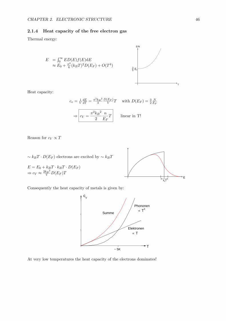
2.1.4 Heat capacity of the free electron gas
Thermal energy:
E =∫∞
0 ED(E)f(E)dE
≈ E0 + π2
6 (kBT )2D(EF ) +O(T 4)
E/N
T
35
EF
Heat capacity:
cv = 1VdEdT = π2kB
2
3D(EF )V T with D(EF ) = 3
2NEF
⇒ cV =π2kB
2
2
n
EFT linear in T!
Reason for cV ∝ T
∼ kBT ·D(EF ) electrons are excited by ∼ kBT
E = E0 + kBT · kBT ·D(EF )
⇒ cV ≈ 2kB2
V D(EF )TE
k TB
Consequently the heat capacity of metals is given by:
Summe
∝ TElektronen
cV
~ 5KT
Phononen∝ T3
At very low temperatures the heat capacity of the electrons dominates!
CHAPTER 2. ELECTRONIC STRUCTURE 47
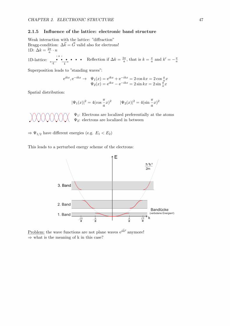
2.1.5 Influence of the lattice: electronic band structure
Weak interaction with the lattice: ”diffraction”Bragg-condition: ∆~k = ~G valid also for electrons!1D: ∆k = 2π
a · n
1D-lattice:a
kk
Reflection if ∆k = 2πa , that is k = π
a and k′ = −πa
Superposition leads to ”standing waves”:
eikx, e−ikx → Ψ1(x) = eikx + e−ikx = 2 cos kx = 2 cos πaxΨ2(x) = eikx − e−ikx = 2 sin kx = 2 sin π
ax
Spatial distribution:
|Ψ1(x)|2 = 4(cosπ
ax)2 |Ψ2(x)|2 = 4(sin
π
ax)2
Ψ1: Electrons are localized preferentially at the atomsΨ2: electrons are localized in between
⇒ Ψ1/2 have different energies (e.g. E1 < E2)
This leads to a perturbed energy scheme of the electrons:
2. Band
1. Band2
Bandlücke(verbotene Energien!)
k
h ²k ²2m
E
ap 2
ap
ap
ap
3. Band
Problem: the wave functions are not plane waves ei~k~r anymore!
⇒ what is the meaning of k in this case?

CHAPTER 2. ELECTRONIC STRUCTURE 48
2.1.6 Bloch-functions
Bloch theorem: the solution of the Schrodinger equation for a periodic system (with a potentialV (~r + ~R) = V (~r) ∀~R) can be written as:
Ψn~k
(~r) = ei~k~r · u
n~k(~r)
where un~k
(~r + ~R) = un~k
(~r) ∀~R
that is the function un~k
(~r) has the same periodicity as the lattice
Remarks: :
• ~k is a quantum number, but not necessarily a wave number
• n is an additional quantum number, which induces different solutions with the same ~k
Appearance of Bloch functions:
r
ikrRe(e )
Re(eikr)
r
U (r)nk
unk(r)(if real )
r Re(eikrunk(r))
Similarity to molecular orbitals!!In fact Bloch functions can be written as Wannier functions:
Ψn~k
(~r) =∑~R
ei~k ~R · ϕn(~r − ~R) Addition of ”atomic orbitals” ϕn(~r)
Localisation of the electrons:
+ almost free electrons z.B. Na (3s-electrons)
localized electrons e.g. Cu (3d-electrons)
CHAPTER 2. ELECTRONIC STRUCTURE 49
The solutions are not unambiguous:
Ψn~k
(~r) = ei~k~r · u
n~k(~r)
can also be written as
Ψn~k
(~r) = ei~k~r · ei ~G~re−i ~G~ru
n~k(~r)
= ei(~k+ ~G)~r · e−i ~G~ru
n~k(~r)︸ ︷︷ ︸
um(~k+~G)
(~r)
um(~k+ ~G)(~r+~R)
= e−i~G(~r+~R)u
n~k(~r + ~R)
= e−i~G~ru
n~k(~r)
= um(~k+ ~G)
(~r)
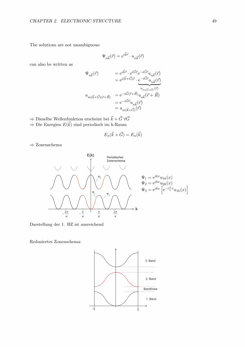
⇒ Dieselbe Wellenfunktion erscheint bei ~k + ~G ∀~G⇒ Die Energien E(~k) sind periodisch im k-Raum
En(~k + ~G) = En(~k)
⇒ Zonenschema
Periodisches Zonenschema
k
E(k)
aπ
aπ2
aπ2
−aπ
−
Ψ2
Ψ3Ψ1
Ψ1 = eikxu1k(x)Ψ2 = eikxu2k(x)
Ψ3 = eikx[e−i
πaxu1k(x)
]
Darstellung der 1. BZ ist ausreichend
Reduziertes Zonenschema:
3. Band
2. Band
1. Band
Bandlücke
aap p
CHAPTER 2. ELECTRONIC STRUCTURE 50
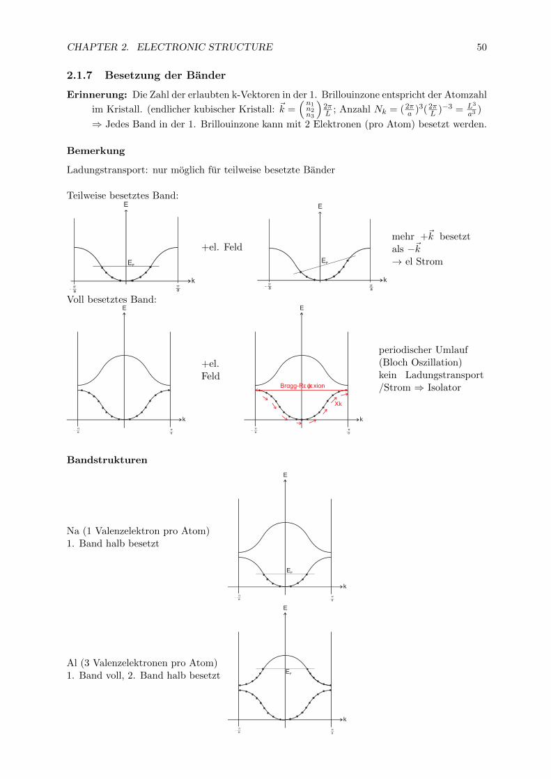
2.1.7 Besetzung der Bander
Erinnerung: Die Zahl der erlaubten k-Vektoren in der 1. Brillouinzone entspricht der Atomzahl
im Kristall. (endlicher kubischer Kristall: ~k =(n1n2n3
)2πL ; Anzahl Nk = (2π
a )3(2πL )−3 = L3
a3 )
⇒ Jedes Band in der 1. Brillouinzone kann mit 2 Elektronen (pro Atom) besetzt werden.
Bemerkung
Ladungstransport: nur moglich fur teilweise besetzte Bander
Teilweise besetztes Band:
k
E
EF
p pa a
+el. Feld
k
E
EF
p paa
mehr +~k besetztals −~k→ el Strom
Voll besetztes Band:
k
E
pa
pa
+el.Feld
k
E
pa
pa
?k
Bragg-Reflexion
periodischer Umlauf(Bloch Oszillation)kein Ladungstransport/Strom ⇒ Isolator
Bandstrukturen
Na (1 Valenzelektron pro Atom)1. Band halb besetzt
k
E
EF
pa
pa
Al (3 Valenzelektronen pro Atom)1. Band voll, 2. Band halb besetzt
k
E
pa
pa
EF

CHAPTER 2. ELECTRONIC STRUCTURE 51
Daraus folgt: Materialien mit ungerader Valenzelektronenzahl pro Atom (und einatomiger Ba-sis) sind Metalle!Bei mehratomiger Basis zahlt die Elektronenzahl pro Basis; Chlor tritt als Cl2 auf und besitztdamit 14 Valenzelektronen. Materialien mit gerader Elektronenzahl pro Basis sind i.A. Isola-toren bzw. Halbleiter; dies gilt aber nicht immer.
“Diamant“ (4 Valenzelektronen)
k
E
pa
pa
EF
Gegenbeispiel: Mg (2 Valenzelektro-nen) ist metallisch: 1. und 2. Bandsind teilbesetzt:
k
E
pa
pa
EF

CHAPTER 2. ELECTRONIC STRUCTURE 52
2.2 Einschub: chemische Bindungen
3 Typen chemischer Bindung:
1. ionische Bindung (stark lokalisierte Elektronen)
2. kovalente Bindung (leicht delokalisierte Elektronen)
3. metallische Bindung ( vollkommen delokalisierte Elektronen)
2.2.1 Ionische Bindung
Zwischen Atomen mit stark unterschiedlichen Ionisationspotenzialen(typ.: Halogen und Metall)
z.B.: LiF
F Li
1s
2s2p
1s
2s
Elektronentransfer
Fuhrt zu starker Coulombanziehung
-F +Li V = − e2
4πε0r
Die Bindungslange wird durch die gefullten inneren Orbitale bestimmt (”Pauli-Abstoßung“)
2.2.2 Kovalente Bindung
Das Elektron geht nicht uber, sondern bleibt ”zwischen“ den AtomenKlassisches Modell fur H+
2 :
+p +
p-
e
r r
Coulombpotential:
Epot =Vep1 + Vep2 + Vp1p2
=− e2
4πε0r− e2
4πε0r+
e2
4πε02r
=− 3
2
e2
4πε0r

CHAPTER 2. ELECTRONIC STRUCTURE 53
Geht gegen unendlich fur r → 0! Ein ”klassisches” Molekul wurde kollabieren! Dies geschiehtnicht, weil das Elektron Wellencharakter hat.
p+ p+
e- - „Wolke“
Die negative Ladungsdichte zwischen den Atomen bestimmt den Gleichgewichtszustand.
Form der Elektronenwolke: Molekulorbitale
Ansatz: Aufbau der Orbitale als Linearkombinationen von Atomorbitalen (LCAO-Linear Com-bination Of Atomic Orbitals)
Beispiel Wasserstoff:
Wellenfunktionender H-Atome
1s
1s
ψ1
ψ2
r1
r2
Wellenfunktionendes H2-Moleküls
ψ1 + ψ2
ψ1 − ψ2
Erhöhte Ladungsdichte
Erniedrigte Ladungsdichte
Es ergeben sich zwei Orbitale, ein bindendes und ein antibindendes. Ob das Molekul insgesamtgebunden ist, hangt von der Besetzung der Molekulorbitale ab. Molekule mit mehreren Elektro-nen folgen dem gleichen Aufbauprinzip wie Atome: alle Orbitale werden mit je zwei Elektronenbesetzt, die niedrigsten zuerst (bei entarteten Orbitalen gilt die Hundt’sche Regel). Damit erhaltman folgende Moglichkeiten fur wasserstoffartige Systeme:
s* antibindendes Orbital+
H2
s bindendes Orbital
1s 1sgebunden
s* antibindendes OrbitalH2
s bindendes Orbital
1s 1sstärkergebunden
s* antibindendes Orbital+
He2
s bindendes Orbital
1s 1sschwächergebunden
s* antibindendes OrbitalHe2
s bindendes Orbital
1s 1srepulsiv!

CHAPTER 2. ELECTRONIC STRUCTURE 54
2.2.3 metallische Bindung
fast homogene Elektronendichte
+ + +
+ + +
+ + +
negative “homogene”Ladungsdichte
Freies Elektronengas mit einge-lagerten Ionen, Gleichgewichtsab-stand bestimmt durch Elektronen-dichte
2.2.4 Kovalente Bindung: lineare Kette
Bei großeren Molekulen ergeben sich die Molekulorbitale analog als Linearkombinationen derAtomorbitale. Wir betrachten den einfachsten Fall, (hypothetische) lineare Ketten aus Wasser-stoffatomen.
Der Einfachkeit halber benutzen wir folgende Darstellung der Orbitale: anstelle des Schnittsdurch die Wellenfunktion zeichnet man eine schematische Equiamplitudenlinie der Wellenfunk-tion; die Farbe (dunkel) bezeichnet eine negative Amplitude der Wellenfunktion.
ψ3
ψ1 bindend
antibindend
H2 ψ3
ψ2
ψ1bindend
nichtbindend
antibindend
H3
Fur Ketten mit drei, vier und funf Atomen erhalt man die Orbitale:
ψ3
ψ2
ψ1 bindend
teilweisebindend
antibindend
H4
ψ4
ψ3
ψ2
ψ1 bindend
teilweiseantibindend
antibindend
H5
ψ4
teilweisebindend
nichtbindend
ψ5
Knotenregel: Je mehr Vorzeichenwechsel der Wellenfunktion, desto hoher dieEnergie!

CHAPTER 2. ELECTRONIC STRUCTURE 55
Unendliche Kette:
a
Ansatz:
Ψk(r) =1√NAt
∑R
eikRϕ(r −R) = |k〉
Schrodingergleichung: H|k〉 = E|k〉
〈k|H|k〉 = E〈k|k〉
⇒ E = 〈k|H|k〉 Erwartungswert der En-ergie im Zustand |k〉
Gilt exakt fur ”‘wahre”’ ϕ; Naherung fur ϕ ∼ ϕAt(LCAO oder ”‘tight-binding”’)
Es ist
E = 〈k|H|k〉 =
∫Ψ∗k(r)H(r)Ψk(r)dr
=1
NAt
∫ ∑R
∑R′
eik(R′−R)H(r)ϕ∗(r −R)ϕ(r −R′)dr | r′ := r −R′
=1
NAt
∑R
∑R′
eik∆R
∫ϕ∗(r′ +R′ −R︸ ︷︷ ︸
∆R
)H(r′ +R′)︸ ︷︷ ︸=H(r′)
ϕ(r′)dr′
=∑∆R
eik∆R
∫ϕ∗(r + ∆R)H(r)ϕ(r)dr
Funktionen ϕ fallen schnell ab ⇒ Integral 6= Null nur fur nachste Nachbarn ⇒ Summation nuruber ∆R = 0,−a, a⇒ E =
∫ϕ∗(r)H(r)ϕ(r)dr︸ ︷︷ ︸
∼ ε0 Orbitalenergie des Atoms
+ e−ika∫ϕ∗(r − a)H(r)ϕ(r)dr︸ ︷︷ ︸
”‘Transferintegral”’ (= -γ)
+ eika∫ϕ∗(r + a)H(r)ϕ(r)dr︸ ︷︷ ︸
auch −γ (ϕ(r) ist symmetrisch)
⇒ E = ε0 − γ2 cos ka Energie von |k〉
mit ε0 Orbitalenergie, γ Transferintegral, k Wellenzahl, a Gitterkonstante
Dispersion:
E(k)
ε0-2γ
-π/a π/a
ε0+2γ
k
1D-Elektronen-Dispersionin "tight-binding"-Näherung
Gilt fur alle fest gebundenen Orbitale eines Atoms im Kristall (bei schwach gebundenen Or-bitalen wird die Beschrankung auf die nachsten Nachbarn ungultig)

CHAPTER 2. ELECTRONIC STRUCTURE 56
Damit ergibt sich die Bandstruktur fur die s- und p-artige atomare Valenzorbitale:
Atomare Orbitale
1s
2p "p"-Band4γp
4γs
E(k)
-π/a π/a
εp
k
εs"s"-Band
atomareEnergien
Krümmung abhängigvom Vorzeichen
von γ
1
2
3
4
Beispiele fur das Aussehen der tight-binding-Orbitalen an wichtigen Punkten der Bandstrukturund der Vergleich mit den entsprechenden Bloch-Funktionen (schwach gestorten ebenen Wellen):
1. k = 0, s-Band: Ψk =
(Vorfaktoren 1, 1, 1, 1, 1, ...)
x
ψ
2. k = πa , s-Band: Ψk =
(Vorfaktoren 1, -1, 1, -1, 1, ...)
x
ψ
3. k = πa , p-Band: Ψk =
(Vorfaktoren 1, -1, 1, -1, 1, ...)
x
ψ
4. k = 0, p-Band: Ψk =
(Vorfaktoren 1, 1, 1, 1, 1, ...)
x
ψ
Die tight-binding- Wellenfunktionen zeigen die gleichen Charakteristika wie die Bloch-Funktionen!

CHAPTER 2. ELECTRONIC STRUCTURE 57
2.2.5 Entwicklung der elektronischen Struktur des Festkorpers
schematisch
Atom Molekul
antibindend
bindend
tragen nichtzur Bindungbei
Festkorper (kontinuierlich)
eher antibindend
eher bindend
besetzte Zustände
kontinuierliches Band
EF
2.2.6 Messung der el. Struktur: Photoelektronen
SpektroskopieAufbau:
Kristall
Vakuum
hν (UV oderRöntgenlicht)
Elektronenemission
e-
e-
e-
Energieanalysator
Detektor
+-
Messung der Energieverteilung der Elektronen durch Variation der Spannung am Detektor
Photoeffekt:Ekin = hν − EBin Einstein
Die kinetische Energie der Elektronen ist die Photonenenergie minus der Bindungsenergie (En-ergieverluste vernachlassigt)

CHAPTER 2. ELECTRONIC STRUCTURE 58
schematisch:
FEF
besetzte Zustandsdichte
Austrittsarbeit
f(E) D(E)
hEkin
0Ekin
gebundene- e
Vakuum
freie -
eν
gemessenes Photoelektronenspektrum
I
Ekinhν-φ0
(gilt nur bei Mittelung uber die Emisssionswinkel)
Messung der Dispersion: Winkelaufgeloste PES
Bestimmung von E(~k): neben Ekin muss der Blochindex k gemessen werden.
Problem: Elektron wird an der Oberflache “gebrochen”.
Vakuum
Kristall
Ekin= E0+hν
Ekin= E0+hν - φ
Aber: Vakuum und Kristall haben parallel zur Oberflache gleiche Periodizitat.(fur Vakuum gilt V (~r) = 0 uberall; und damit V (~r + ~R) = V (~r))⇒ ~k|| ist Erhaltungsgroße!
θ
|| |~k′| =√
2m~2 Ekin
| ~k||| =√
2m~2 EkinsinΘ

CHAPTER 2. ELECTRONIC STRUCTURE 59
⇒ Projizierte Dispersion E( ~k||) ergibt sich aus winkelaufgelosten Spektren I(Θ, En).
Volle Dispersion (E(~k)): “tomographisches Verfahren”: Projektion von ~k auf verschiedene Ebe-nen im Kristall.⇒ Messung von Winkelaufgelosten Spektren an verschiedenen Oberflachen (z.B.: (1 1 1), (1 00),..
2.2.7 Fermiflachen
Fermiflache: Equienergieflache im k-Raum mit E(~k) = EF .Kugelflache bei realen Metallen:
kF
Bsp.: Cu, Ag
<111>
kF
Schnitte:
EF
k
E(k)
0aπ3
aπ3
−
k
E(k)
EF
kF aπ2
aπ2
−
Noch komplexeres Verhalten bei mehrwertigen Metallen:Volumen innerhalb einer Fermiflache:
VFF =NV al
2︸ ︷︷ ︸Zahl der Valenzel.
V1.BZ︸ ︷︷ ︸Volumen 1.BZ
⇒ Fermiflache ist fur NV al ≥ 2 nicht auf die 1. BZ beschrankt
2.2.8 Bewegungsgleichungen
Blochfunktion fur Elektronen:Ψnk(~r) = ei
~k~runk(~r)

CHAPTER 2. ELECTRONIC STRUCTURE 60
mit Energie Enk = En(~k).Die Gruppengeschwindigkeit ist(wie bei freien Teilchen):
vGr =dω(k)
dk=
1
~dE
dk
Die Energieanderung bei Bewegung im elektrischen Feld ε ist
∆E = −eε∆x = −eεVg∆t
Dies wird mit ∆E =dE
dk∆k zu
dE
dk∆k = −eε1
~dE
dk∆t
∆k
∆t= k = −eε
~Anderung vom Blochindex im elektrischen Feld
(freies Teilchen: p = F = −eε ⇒ ~k = −eε ⇒ k = −e ε~)
Das bedeutet: der Blochindex k ist ein “Quasiimpuls” (verhalt sich wie ein Impuls, obwohlkeine Impulserhaltung gilt)
Geschwindigkeitsanderung
vg =d
dt(1
~dE
dk) =
1
~d2E
dk2
dk
dt=
1
~2
d2E
dk2(−eε)
Freies Teilchen:
v =p
m=
1
m(−eε)
Damit kann man eine effektive Masse definieren:
meff =~2
d2Edk2
d2Edk2 ist die Krummung der Dispersionskurve!
k
E
starkeKrümmung
“leichtes“ Teilchen: starkeGeschwindigkeitszunahme im el. Feld
k
E
schwacheKrümmung
“schweres“ Teilchen: geringeGeschwindigkeitszunahme im el. Feld
gilt fur samtliche kristalline Materialien⇒ Elektronen im Gitter verhalten sich wie freie Elektronen mit anderen Massen.
CHAPTER 2. ELECTRONIC STRUCTURE 61
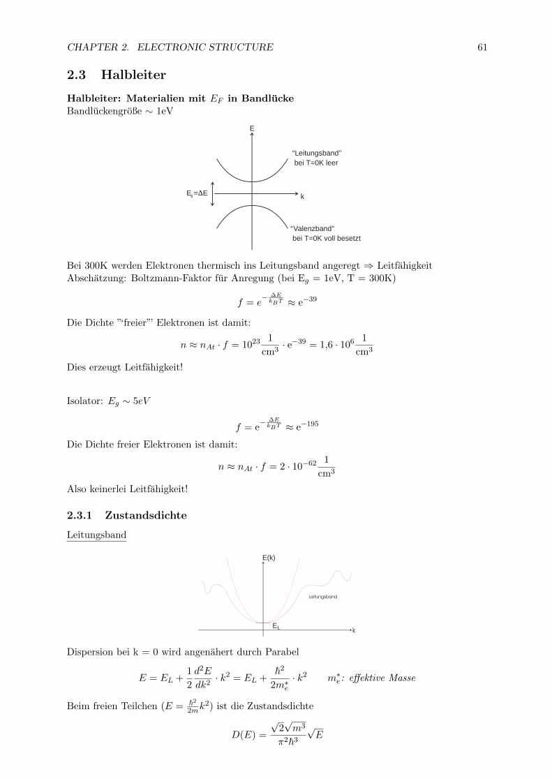
2.3 Halbleiter
Halbleiter: Materialien mit EF in BandluckeBandluckengroße ∼ 1eV
k
E
E = Eg
“Leitungsband” bei T=0K leer
“Valenzband” bei T=0K voll besetzt
∆
Bei 300K werden Elektronen thermisch ins Leitungsband angeregt ⇒ LeitfahigkeitAbschatzung: Boltzmann-Faktor fur Anregung (bei Eg = 1eV, T = 300K)
f = e− ∆EkBT ≈ e−39
Die Dichte ”‘freier”’ Elektronen ist damit:
n ≈ nAt · f = 1023 1
cm3· e−39 = 1,6 · 106 1
cm3
Dies erzeugt Leitfahigkeit!
Isolator: Eg ∼ 5eV
f = e− ∆EkBT ≈ e−195
Die Dichte freier Elektronen ist damit:
n ≈ nAt · f = 2 · 10−62 1
cm3
Also keinerlei Leitfahigkeit!
2.3.1 Zustandsdichte
Leitungsband
k
E(k)
Leitungsband
EL
Dispersion bei k = 0 wird angenahert durch Parabel
E = EL +1
2
d2E
dk2· k2 = EL +
~2
2m∗e· k2 m∗e: effektive Masse
Beim freien Teilchen (E = ~2
2mk2) ist die Zustandsdichte
D(E) =
√2√m3
π2~3
√E

CHAPTER 2. ELECTRONIC STRUCTURE 62
Im Leitungsband des Halbleiters ist die Dispersion bis auf die andere (nun effektive) Masse unddie Verschiebung des Energie-Nullpunkts gleich; damit muss die Zustandsdichte hier lauten:
DL(E) =
√2√m∗e
3
π2~3
√E − EL Leitungsband
Valenzband
Ev
E(k)
k
E = EV −~2
2m∗h· k2 m∗h: effektive Masse der Elektronen
im Valenzband (”‘Lochermasse”’)
DV (E) =
√2√m∗h
3
π2~3
√EV − E Valenzband
2.3.2 Besetzungswahrscheinlichkeit
Temperatur T = 0K
EF
D(E)
EVB LB
EV EL
Eg
LB leer
VB besetzt
D(E)
E
Temperatur T > 0K
LBVB
D(E)
E
thermischangeregt
Beschrieben mit Fermi-Dirac-Funktion
f(E) =1
eE−µkBT + 1
µ chemisches Potential
CHAPTER 2. ELECTRONIC STRUCTURE 63
Zustandsdichte Besetzungswahrscheinlichkeit besetzte ZustandeD(E)
EE
1
0,5
µ
k TB
f(E)D(E)
EEL
Zahl der Elektronen im Leitungsband
n =
∞∫EL
DL(E) · fT (E)dE
Zahl der fehlenden Elektronen im Valenzband (”‘Locherdichte”’)
p =
EV∫−∞
DV (E)(1− fT (E))dE
Einsetzen und integrieren:
n = 14
(2m∗ekBTπ~2
) 32
e−−(EL−µ)
kBT
p = 14
(2m∗hkBTπ~2
) 32
e−−(µ−EV )
kBT
Produkt:
np = 4(kBT2π~2
)3(m∗em
∗h)
32 e− EgkBT
”‘Massenwirkungsgesetz”’: np konstant auch fur n 6= p
Beispiele: Eg np (300K)Si 1,11 eV 2,1 ·109cm−6
Ge 0,64 eV 2,89 ·1029cm−6
GaAs 1,43 eV 6,55 ·1012cm−6
”‘Intrinsische”’ Halbleiter (n=p)⇒ n =
√n · p (Si: n = 4,6 ·109 1
cm3 )
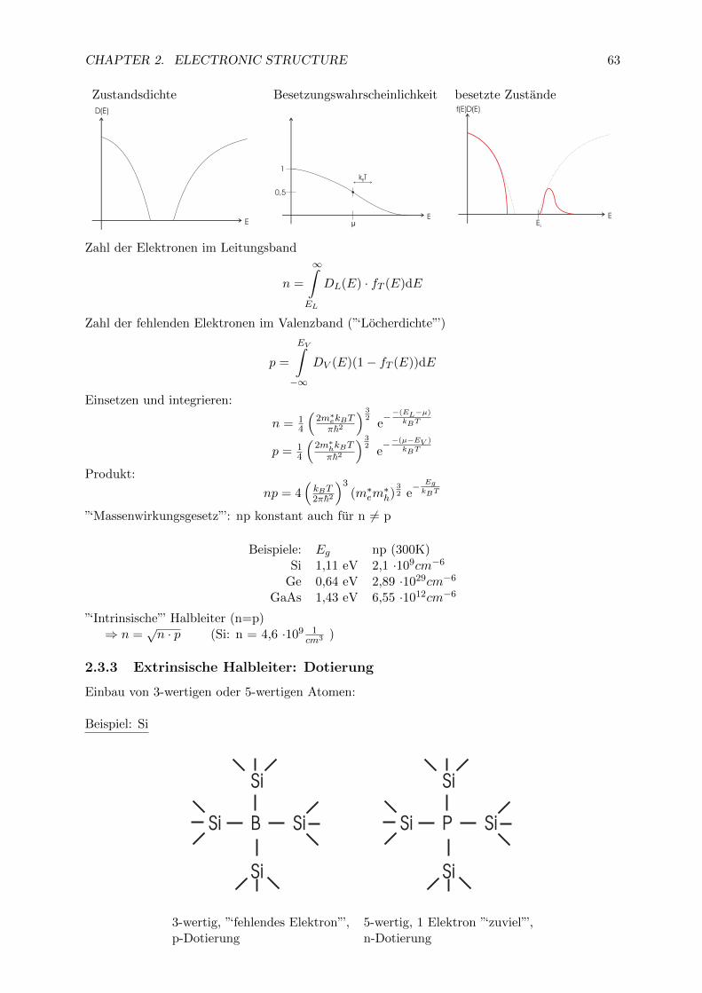
2.3.3 Extrinsische Halbleiter: Dotierung
Einbau von 3-wertigen oder 5-wertigen Atomen:
Beispiel: Si
B
Si
SiSi
Si
P
Si
SiSi
Si
3-wertig, ”‘fehlendes Elektron”’, 5-wertig, 1 Elektron ”‘zuviel”’,p-Dotierung n-Dotierung

CHAPTER 2. ELECTRONIC STRUCTURE 64
Durch geringe thermische Energie kann das Elektron (oder Loch) des Dotieratoms freigesetztwerden.
Vgl.: Bohr-Atom (Wasserstoff)
+p
-eBindungsenergie des Elektrons: E = Ry
1
n2=
mee4
2(4πεε0~)2
1
n2
Bahnradius: r = 4πεε0~2
mee2n2
Dotieratom:
P
Si
SiSi
Si
+
-e E =m∗eme
1
ε2
Ryn2
r = a0 = εme
m∗en2a0
typisch: m∗e ∼ 110me ε ∼ 10
⇒ E = 11000Ry = 13,6meV ; R = 100a0 ≈ 50A
⇒ bei kBT = E (T ≈ 140K) werden alle Elektronen freigesetzt.
B
Si
SiSi
Si
+ Gleiches gilt fur Locher:Ebenfalls Bindungsenergie des Lochs von ∼10meV
Damit Energieschema:
Donator
EL10meV
EV
n-Halbleiter
n-dotiert
Akzeptor
EL
10meV
EV
p-Halbleiter
p-dotiert
Die freigesetzten Ladungstrager erzeugen Leitfahigkeit!
2.3.4 Temperaturabhangigkeit
n-Halbleiter, tiefe Temperaturen
ED EL
LBVB
D(E)
E
µ
Ein Teil der Donatoren ist ionisiertAlle Elektronen im Leitungsband stammen von Donatoren
CHAPTER 2. ELECTRONIC STRUCTURE 65
⇒ chemisches Potential µ liegt zwischen dem ED und EL
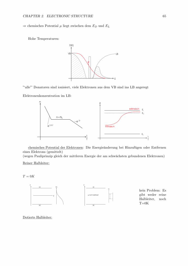
Hohe Temperaturen:
LBVB
D(E)
E
µ
”‘alle”’ Donatoren sind ionisiert, viele Elektronen aus dem VB sind ins LB angeregt
Elektronenkonzentration im LB:
n
1 T
e-E /k Tg B
n=ND
~e-
E-El D
k TB
EL
EV
ED
1 T
µ
intrinsisch
extrinsisch
chemisches Potential der Elektronen: Die Energieanderung bei Hinzufugen oder Entferneneines Elektrons (gemittelt)(wegen Pauliprinzip gleich der mittleren Energie der am schwachsten gebundenen Elektronen)
Reiner Halbleiter:
T = 0K
µ
E
LB
VB
f(E)
µ nicht definiert
E
LB
VB
f(E)
kein Problem: Esgibt weder reineHalbleiter, nochT=0K
Dotierte Halbleiter:
CHAPTER 2. ELECTRONIC STRUCTURE 66
µ
E
LB
VB
Ed
f(E)
Bringt man Systeme mit unterschiedlichen µ zusammen, wechseln Teilchen vom System mitgroßem µ zum System mit kleinem µ (Energiegewinn!).
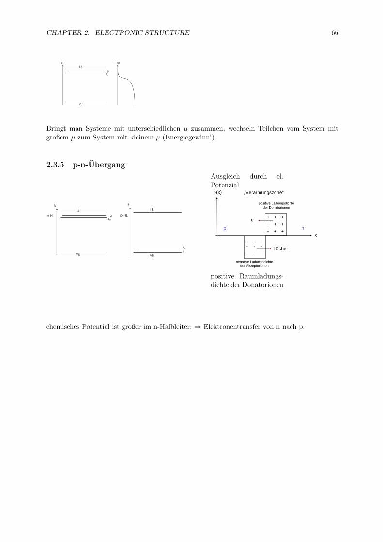
2.3.5 p-n-Ubergang
µ
E
LB
VB
ED
n-HL
µ
E
LB
VB
EA
p-HL
Ausgleich durch el.Potenzial
+ + ++ + ++ + +
- - -- - -- - -
e-
Löcher
„Verarmungszone“
positive Ladungsdichteder Donatorionen
negative Ladungsdichteder Akzeptorionen
ρ(x)
xnp
positive Raumladungs-dichte der Donatorionen
chemisches Potential ist großer im n-Halbleiter; ⇒ Elektronentransfer von n nach p.
CHAPTER 2. ELECTRONIC STRUCTURE 67
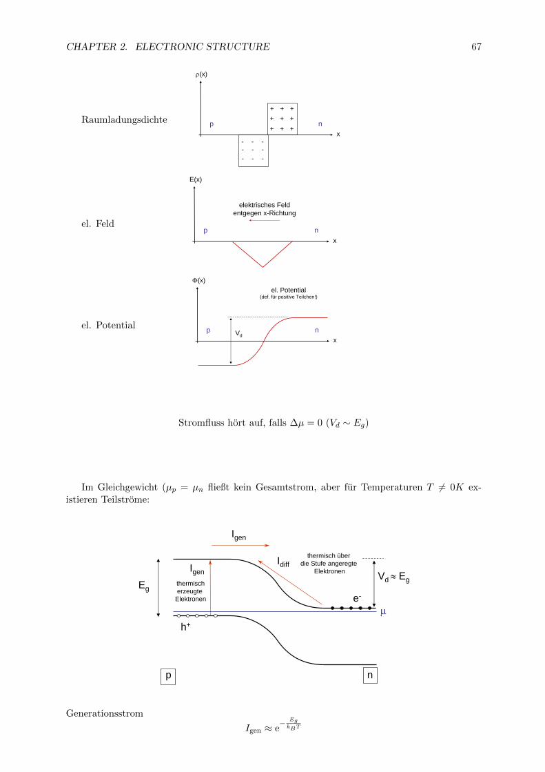
Raumladungsdichte+ + ++ + ++ + +
- - -- - -- - -
ρ(x)
xnp
el. Feld
E(x)
x
elektrisches Feldentgegen x-Richtung
np
el. Potential
Φ(x)
x
el. Potential(def. für positive Teilchen!)
Vdnp
Stromfluss hort auf, falls ∆µ = 0 (Vd ∼ Eg)
Im Gleichgewicht (µp = µn fließt kein Gesamtstrom, aber fur Temperaturen T 6= 0K ex-istieren Teilstrome:
μ
p n
Eg
Idiffthermisch über
die Stufe angeregte ElektronenIgen
thermischerzeugte
Elektronen e-
h+
Vd ≈ Eg
Igen
Generationsstrom
Igen ≈ e− EgkBT
CHAPTER 2. ELECTRONIC STRUCTURE 68
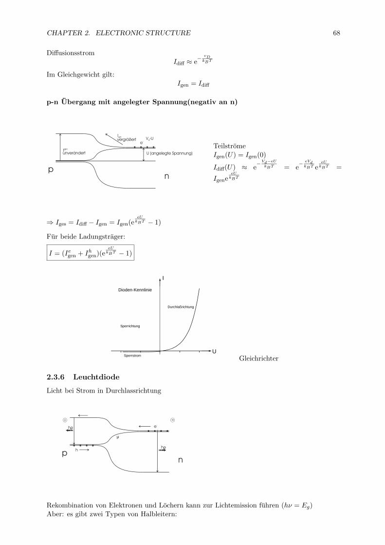
DiffusionsstromIdiff ≈ e
− vDkBT
Im Gleichgewicht gilt:Igen = Idiff
p-n Ubergang mit angelegter Spannung(negativ an n)
pn
Idiff
-e
genIunverändert
vergrößert V -Ud
U (angelegte Spannung)
TeilstromeIgen(U) = Igen(0)
Idiff(U) ≈ e−Vd−eU
kBT = e− eVdkBT e
eUkBT =
IgeneeUkBT
⇒ Iges = Idiff − Igen = Igen(eeUkBT − 1)
Fur beide Ladungstrager:
I = (Iegen + Ihgen)(eeUkBT − 1)
Sperrstrom
Durchlaßrichtung
U
I
Dioden-Kennlinie
Sperrichtung
Gleichrichter
2.3.6 Leuchtdiode
Licht bei Strom in Durchlassrichtung
pn
-eh?
µ
h?
+ -
h
Rekombination von Elektronen und Lochern kann zur Lichtemission fuhren (hν = Eg)Aber: es gibt zwei Typen von Halbleitern:

CHAPTER 2. ELECTRONIC STRUCTURE 69
Direkte Halbleiter:
schematische Bandstruktur
E
k
hν Eg
Valenzband
Leitungsband
Minimum des Leitungsbandes liegt uber dem Maximum des Valenzbandes (bei gleichem k)Fur kleinstmogliche Anregung (hν = Eg) gilt ∆k = 0. ⇒ gute Absorption/EmissionAbsorptionsspektrum:
Absorption
hνEg
transparent
Indirekte Halbleiter:
schematische Bandstruktur
E
k
Eg
Valenzband
Leitungsband
PhotonPhononEg
d
Das Minimum des Leitungsbandes liegt nicht uber dem Maximum des Valenzbandes.Minimale Anregung ist nur moglich mit Beteiligung eines Phonons.Bei der Absorption/Emission gilt: Energie- und (Quasi-)Impulserhaltung.(∆Eges = 0, ∆kges = 0)In diesem Fall gilt:
Energie-Erhaltung:∆EElektron = hνPhoton ± hνPhonon
“Impuls”-Erhaltung:
∆~kel. = ~kPhonon ± ~kPhoton
Erinnerung:
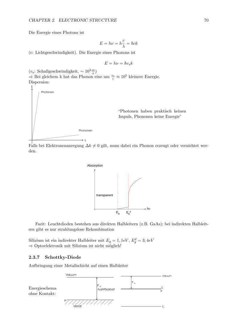
CHAPTER 2. ELECTRONIC STRUCTURE 70
Die Energie eines Photons ist
E = hν = hc
λ= ~ck
(c: Lichtgeschwindigkeit). Die Energie eines Phonons ist
E = hν = ~vsk
(vs: Schallgeschwindigkeit, ∼ 103ms )
⇒ Bei gleichem k hat das Phonon eine um vsc ≈ 105 kleinere Energie.
Dispersion:
Photonen
Phononen
k
E
“Photonen haben praktisch keinenImpuls, Phononen keine Energie”
Falls bei Elektronenanregung ∆k 6= 0 gilt, muss dabei ein Phonon erzeugt oder vernichtet wer-den.
Absorption
hνEg
transparent
Egd
Fazit: Leuchtdioden bestehen aus direkten Halbleitern (z.B. GaAs); bei indirekten Halbleit-ern gibt es nur strahlungslose Rekombination
Silizium ist ein indirekter Halbleiter mit Eg = 1, 1eV , Edg = 3, 4eV⇒ Optoelektronik mit Silizium ist nicht moglich!
2.3.7 Schottky-Diode
Aufbringung einer Metallschicht auf einen Halbleiter
Energieschemaohne Kontakt:
Vakuum
Metall
Austrittsarbeit
F M
µ
Vakuum
µEL
EV
F HL
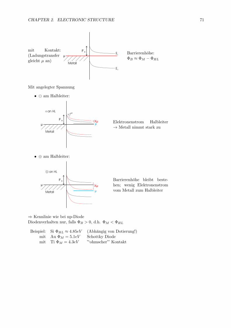
CHAPTER 2. ELECTRONIC STRUCTURE 71
mit Kontakt:(Ladungstransfergleicht µ an)
µ
Metall
EL
EV
F B Barrierenhohe:ΦB ≈ ΦM − ΦHL
Mit angelegter Spannung
• am Halbleiter:
µ
Metall
F B ?µ
diffI
µ
- an HL
Elektronenstrom Halbleiter→ Metall nimmt stark zu
• ⊕ am Halbleiter:
µMetall
F B
?µµ
+ an HL
Barrierenhohe bleibt beste-hen; wenig Elektronenstromvom Metall zum Halbleiter
⇒ Kennlinie wie bei np-DiodeDiodenverhalten nur, falls ΦB > 0, d.h. ΦM < ΦHL
Beispiel: Si ΦHL ≈ 4.85eV (Abhangig von Dotierung!)mit Au ΦM = 5.1eV Schottky Diodemit Ti ΦM = 4.3eV ”‘ohmscher”’ Kontakt
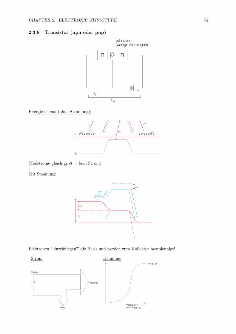
CHAPTER 2. ELECTRONIC STRUCTURE 72
2.3.8 Transistor (npn oder pnp)
n p n
sehr dünn(wenige Atomlagen)
- + - +UEB
UEK
Energieschema (ohne Spannung):
EV
EL
µ
diffI
genI
diffI
e- e
-
(Teilstrome gleich groß ⇒ kein Strom)
Mit Spannung:
diffIgrößer!
UEB
UEK
UEB
Elektronen ”‘durchfliegen”’ die Basis und werden zum Kollektor beschleunigt!
Strom Kennlinie
Kollektor
Basis
Emitter
I
IEK
UEB
Sättigung
Arbeitspunkt(max. Steigung)

CHAPTER 2. ELECTRONIC STRUCTURE 73
2.3.9 FET (Feld-Effekt-Transistor)
n-HL
Metall
Isolator
p-HL
DrainGateSource
Spannung an ”‘Gate”’ steuert den Strom zwischen Source und Drain
Energieschema:
• Keine Spannung am Gate
µ
EL
EV
Metall(Gate)
Barriere HL
µ
⇒ Source-Drain entspricht npn-ubergang mit UEB = 0⇒ kein Stromfluss
• Positive Spannung am Gate
µ
EL
EV
µ
UG
Absenkung des Leitungsbandes unter µ⇒ 2D-Elektronengas
pn n
- + +
-“2D-e -Gas” An der Grenzflache:
⇒ n-”‘n”’-n-ubergang⇒ Strom zwischen Source und Drain
Kein Strom am Gate: stromsparender als n-p-n Transistor

CHAPTER 2. ELECTRONIC STRUCTURE 74
2.4 Isolatoren
große Bandlucke (> 5 eV)⇒ - keine freien Elektronen bei T = 300K (nicht leitfahig)
- transparent im Sichtbaren
Absorption
UV
transparent
sichtbar
EG
Einschub: Exzitonen
Gebundene Elektron-Loch-Zustande⇒ Anregungsenergie < Eg
Exitonen gibt es bei allen direkten Hal-bleitern und IsolatorenFuhren zu ”‘Rydberg”’-Serie im Absorption-sspektrum
ExzitonenLB
VBEg -e
+
HL
atomartigerZustand
Atom Isolator
1/n²-Serie
h?
Absorption
13,61
Atom:Isolator:
EG
Exzitonen
⇒ Einsatz eines Absorptionsspektrums liegt bei hν < Eg
2.4.1 Optische Eigenschaften von Isolatoren (Dieelektrika)
Keine Absorption; trotzdem Wechselwirkung mit Licht durch Polarisierung (vgl. 2.1.1)
Dipoldichte: ~p = (ε− 1)ε0~E ≈ α~E
⇒ ε(ω) = 1 + 1ε0α(ω) | Achtung, Naherung!
α(ω) = NAtV αAt
(Polarisierbarkeit pro Volumen, αAt atomare Polarisierbarkeit)

CHAPTER 2. ELECTRONIC STRUCTURE 75
Modell fur Atom: Elektron an Feder-
e+
=
Differentialgleichung (gedampfter harmonischer Oszillator):
mu = −Du− βu+ eE0e−iωt
(D Federkonstante, β Reibung, E0e−iωt elektrisches Feld)
Ansatz: u(t) = u0e−iωt
⇒ −ω2mu0 = −Du0 + iωβu0 + eE0
⇒ u0 =eE0
m(Dm − ω2)− iωβ=
eE01m
(ω20 − ω2)− iωτ
∣∣∣∣∣ω0 =√
Dm
τ = mβ
Damit ist das Dipolmoment des Atoms
PAt = e · u(t)
und die Polarisierbarkeit (Naherung fur die harmonische Kraft)
αAt =PAtE0
=e2
m
(ω20 − ω2)− iωτ
Dielektrische Funktion:
ε(ω) = 1 + 1ε0Nv αAt = ε1(ω) + iε2(ω)
0
1
2
3
ε1
ε2
ω0
Dielektrische Funktion
ω
ε(ω)
Maximales |ε| bei Resonanzenergie ω0! (bei der Absorptionsenergie)Elektronischer Anteil: Bei Kristallen mit unterschiedlichen Atomen gibt es zusatzlich einenGitteranteil zur Polarisation.Polarisierbarkeit:
α = αel + αion
⇒ gesamte dielektrische Funktion:
1
? el
e (1 ? )
?
estat
? Ion

CHAPTER 2. ELECTRONIC STRUCTURE 76
Der Brechungsindex ist gegeben durch n =√ε genauer n = Re
√ε1 + ε2.
Damit gilt fur die meisten Dielektrika:n
?rot blau
“normale” Dispersion (gilt nicht mehr imFerninfrarot oder fernen UV)
2.4.2 Clausius-Mossotti
Tatsachlich werden Atome nicht durch ein außeres Feld polarisiert, sonder auch durch das Feldpolarisierter Nachbaratome. ⇒ Ruckkopplung⇒ im Allgemeinen gilt: ε(ω) wird großer als 1 + α
εEs gilt:
ε− 1
ε+ 2=
1
3ε0
∑j
εjNj
Vjαj Clausius-Mossotti
αj : verschiedene Anteile der Polarisierbarkeit
umgeformt:
ε =3ε0 + 2
∑ NjV αj
3ε0 −∑ Nj
V αj= 1 +
∑ NjV αj
ε0 − 13
∑ NjV αj
Diskussion :fur αj → 0 oder
NjV → 0 gilt ε→ 1 + 1
ε0
∑jNjV αj
fur∑
jNjV αj → 3ε0 gilt ε→∞
Letzteres fuhrt zu unterschiedlichen Effekten,je nachdem, ob die Dipoldichte elektronischer oderionischer Herkunft ist.
Elektronen: ein unendlicher Wert von ε ist das Kennzeichen eines Metalls. Daraus folgt:
1. Alle Materialien werden bei großem Druck (großer Dichte) metallisch
2. Aus Atomdichte und -polarisierbarkeit lasst sich direkt vorhersagen, ob ein Material met-allisch ist.
Ionen: bei richtigen Werten von Dichte und Polarisierbarkeit bildet sich eine permanente Dipoldichteaus (ferroelektrisches Verhalten).
2.4.3 Ferroelektrizitat
Atome verschieben sich⇒permanenter Dipol
+ ++
+ ++
+ ++
- -
- -
geschieht nur unterhalb kritis-cher Temperatur Tc
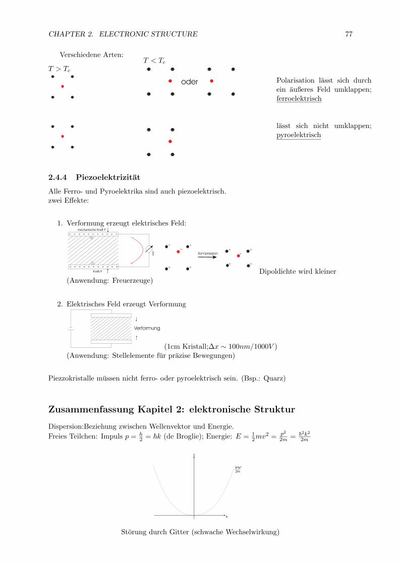
CHAPTER 2. ELECTRONIC STRUCTURE 77
Verschiedene Arten:
T > Tc
T < Tc
oder Polarisation lasst sich durchein außeres Feld umklappen;ferroelektrisch
lasst sich nicht umklappen;pyroelektrisch
2.4.4 Piezoelektrizitat
Alle Ferro- und Pyroelektrika sind auch piezoelektrisch.zwei Effekte:
1. Verformung erzeugt elektrisches Feld:
I
+
- - - - - - - - - - -
+ + + + + + + + + +
+
-
mechanische Kraft F
Kraft F
+ +
+ +
- + +
+ +
-Kompression
Dipoldichte wird kleiner(Anwendung: Freuerzeuge)
2. Elektrisches Feld erzeugt Verformung
Verformung
(1cm Kristall;∆x ∼ 100nm/1000V )(Anwendung: Stellelemente fur prazise Bewegungen)
Piezzokristalle mussen nicht ferro- oder pyroelektrisch sein. (Bsp.: Quarz)
Zusammenfassung Kapitel 2: elektronische Struktur
Dispersion:Beziehung zwischen Wellenvektor und Energie.
Freies Teilchen: Impuls p = h2 = ~k (de Broglie); Energie: E = 1
2mv2 = p2
2m = ~2k2
2m
k
h²k²2m
E
Storung durch Gitter (schwache Wechselwirkung)

CHAPTER 2. ELECTRONIC STRUCTURE 78
k
h²k²2m
E
Aufspaltungfür k = 1/2 G
π2πaa a a
π 2π
Aufspaltung fur ~k = 12~(G)
(Bragg-Reflektion:~k → −~k)⇒ ∆~k = α~k = ~G
Sehr starke Wechselwirkung
=
Praktisch keine Abhangigkeit von k
Darstellung durch Blochfunktionen:
pa
pa
3. Band
2. Band
1. Band
Bandlücke
1. BrillouinzoneE
k
1.Brillouinzone:
• Einheitszelle des reziproken Gitters
• enthalt 1. reziproken Gittervektor
• hat Symmterie des Gitters (Wigner-Seitz-Zelle)
• bei endlichen Kristallen (diskrete k-Werte): enthalt NGP erlaubte Gittervektoren(NGP : Zahl der Gitterpunkte im realen Kristall = Zahl der Atome bei 1Atom
Gitterpunkt
Damit ist die Bandstruktur:
k
E
erlaubte Elektronen-Zustände(können mit 2 Elektronenbesetzt werden)
1. Band
2. Band (Entartung möglich!)
N erlaubte k-WerteGP
aππ
a
erlaubte Elektronenzustande(konnen mit 2 Elektronen besetzt werden)⇒ Zahl der besetzten Bander= NEl
2NGP

CHAPTER 2. ELECTRONIC STRUCTURE 79
Besetzung der Bander bestimmt Materialeigenschaften:
besetzt
unbesetzt
EF
E
D(E)Metall (1-wertig)
EF
E
D(E)Metall (2-wertig)
EF
E
D(E)Halbleiter
1eV EF
E
D(E)Isolator
5eV