advanced imager technology development at mit ... - eso · mit lincoln laboratory eso-dfa-1 vs...
TRANSCRIPT
MIT Lincoln Laboratory
ESO-DFA-1 VS 10/13/09
Advanced Imager Technology
Development at MIT Lincoln
Laboratory
Vyshnavi Suntharalingam [email protected]
Barry E. Burke, James Gregory, Robert K. Reich MIT Lincoln Laboratory
Detectors for Astronomy, ESO Garching 12-16 October 2009
The MIT Lincoln Laboratory portion of this work was performed in part under a Collaboration Agreement between MIT Lincoln Laboratory and University of
Hawaii (Pan-STARRs), sponsored in part by NASA, and the Air Force under the Department of the Air Force contract number FA8721-05-C-0002. Opinions,
interpretations, conclusions, and recommendations are those of the authors and are not necessarily endorsed by the United States Government.

MIT Lincoln Laboratory ESO-DFA-2 VS 10/13/09
Outline
• Overview of MIT-LL X-ray, visible to NIR imaging technology
– Tiled CCD Imagers for astronomy
– Devices for adaptive optics
– Back-illumination processes
• Next-generation technologies
– Stitched large-format, small-pixel CCDs
– Four-side abuttable CCD and 3-D CMOS image sensors
• Summary
MIT Lincoln Laboratory ESO-DFA-3 VS 10/13/09
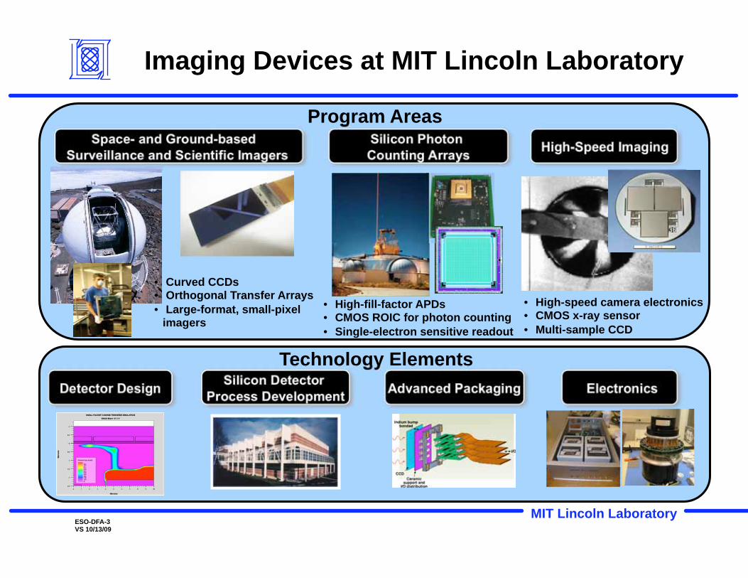
Imaging Devices at MIT Lincoln Laboratory
Space- and Ground-based
Surveillance and Scientific Imagers High-Speed Imaging
Silicon Photon
Counting Arrays
Program Areas
Technology Elements Silicon Detector
Process Development Detector Design Advanced Packaging Electronics
• Curved CCDs • Orthogonal Transfer Arrays
• Large-format, small-pixel imagers
• High-fill-factor APDs • CMOS ROIC for photon counting
• Single-electron sensitive readout
• High-speed camera electronics • CMOS x-ray sensor
• Multi-sample CCD

MIT Lincoln Laboratory ESO-DFA-4 VS 10/13/09
Microelectronics Facility Upgrade to 200-mm Silicon Wafer Size
150-mm waferSix devices
100-mm waferTwo devices (2K x 4K)
• Three-year capability upgrade in progress
– First 200-mm device lots beginning Feb. 2011
200-mm waferNine devices
illustration
CCID-20
CCID-20
• Nine CCID-20s on a 200-mm wafer
– 15- m pixel, 2K x 4K, 32mm x 63mm

MIT Lincoln Laboratory ESO-DFA-5 VS 10/13/09
Tiled CCD Imagers for Astronomy
60 Orthogonal-Transfer CCDs
Pan-STARRs (3° WFOV)
1.36 Gpixels 12-CCD UH/CFHT FPA
100Mpix Image from First Light
(August 2007)
200 m
1.2 mm
MIT Lincoln Laboratory ESO-DFA-6 VS 10/13/09
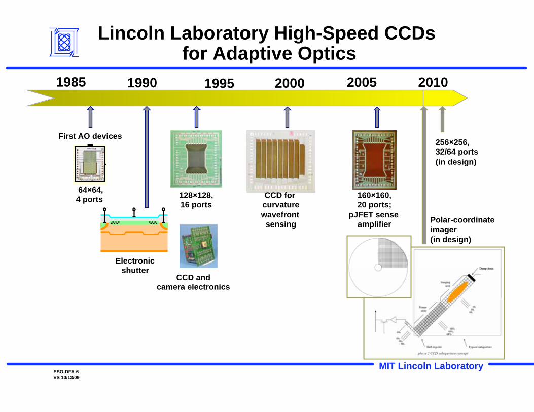
Lincoln Laboratory High-Speed CCDs for Adaptive Optics
1990 2000 1985 1995 2005 2010
First AO devices
64 64, 4 ports
CCD and camera electronics
128 128, 16 ports
160 160, 20 ports;
pJFET sense amplifier
256 256, 32/64 ports
(in design)
Electronic shutter
CCD for curvature
wavefront sensing
Polar-coordinate imager
(in design)

MIT Lincoln Laboratory ESO-DFA-7 VS 10/13/09
Performance of pJFET-based Output Circuit
Noise: pJFET vs. nMOSFET
Am
plifi
er
read
no
ise
(rm
s e
lectr
on
s)
Output Data Rate (MHz)

MIT Lincoln Laboratory ESO-DFA-8 VS 10/13/09
Output Circuit Comparison
Sense-node capacitance is lower ( higher responsivity) for JFET
than MOSFET
Noise spectral voltage is lower for JFET than MOSFET
MIT Lincoln Laboratory ESO-DFA-9 VS 10/13/09
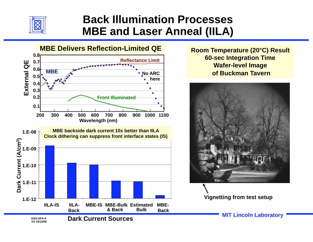
Back Illumination Processes MBE and Laser Anneal (IILA)
MBE Delivers Reflection-Limited QE Room Temperature (20°C) Result
60-sec Integration Time
Wafer-level Image
of Buckman Tavern
Vignetting from test setup 1.E-12
1.E-11
1.E-10
1.E-09
1.E-08
IILA-IS IILA-Back
MBE-IS MBE-Bulk & Back
Estimated Bulk
MBE-Back
Dark Current Sources
Dark
Cu
rren
t (A
/cm
2)
MBE backside dark current 10x better than IILA Clock dithering can suppress front interface states (IS)
200 600 700 800 900 500 400 300 1000 1100 Wavelength (nm)
0.8
0.7
0.6
0.5
0.4
0.3
0.2
0.1
Exte
rnal
QE
Front Illuminated
Reflectance Limit
MBE No ARC here
MIT Lincoln Laboratory ESO-DFA-10 VS 10/13/09
Outline
• Overview of MIT-LL X-ray, visible to NIR imaging technology
– Tiled CCD Imagers for astronomy
– Devices for adaptive optics
– Back-illumination processes
• Next-generation technologies
– Stitched large-format, small-pixel CCDs
– Four-side abuttable, 3-D CMOS image sensors
• Summary

MIT Lincoln Laboratory ESO-DFA-11 VS 10/13/09
Deeply Scaled CCD Process Technology
• Small pixels, low-voltage, CMOS-compatible operation
• Demonstrated small-array CCDs
– Simplified single and two poly fabrication
– Reduced pixel dimension (8-, 5-, 2-μm)
– ~150,000 e- well capacity for 8-μm pixel at 3V
• Current efforts: Apply to large area devices
– Deep ultraviolet photolithography for submicron features (pixel sizes to 2
m)
– Stitching for large format imagers
10μm
10μm
Single Poly OTCCD
10μm
Two Poly OTCCD
5-μm
pixel
8-μm
pixel
2- m
pixel CCD

MIT Lincoln Laboratory ESO-DFA-12 VS 10/13/09
Large-Format, Modular CCD Imagers
• Example: 3K x 3K OTCCD image sensor with 8 m x 8 m pixels
• Pixels with submicron dimensions require high-resolution (248-nm) patterning
– Lithography field size is smaller than device size
• Design is fractured into functional blocks onto a multi-field reticle and precisely stitched back together on wafer
Design Concept Layout Fractured
Functional Blocks Reassembled Design on Wafer Multi-field Reticle

MIT Lincoln Laboratory ESO-DFA-13 VS 10/13/09
Completed 3K x 3K OTCCD Devices
• Large-area devices (26 mm x 50 mm) fabricated with low-voltage CCD technology
• Stitching methods achieve 35nm (3 ) precision with 8- m pixel active devices
• Device test results expected in Dec. 2009
• Process technology will be migrated to 200-mm substrates
single poly
Frame Store
dual poly
OT Image Array
8 m
300 nm
Stitched
Boundary Reference Image (No Stitching Required)
Stitch boundary
300 nm
Poly-1 gate
channel
stop
1 m 1 m
150 mm
MIT Lincoln Laboratory ESO-DFA-14 VS 10/13/09
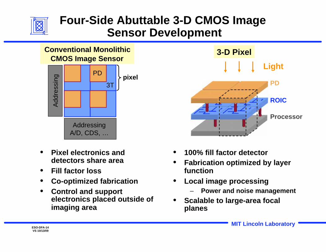
• Pixel electronics and detectors share area
• Fill factor loss
• Co-optimized fabrication
• Control and support electronics placed outside of imaging area
Conventional Monolithic
CMOS Image Sensor 3-D Pixel
pixel
Addressing
A/D, CDS, …
Addre
ssin
g
• 100% fill factor detector
• Fabrication optimized by layer function
• Local image processing
– Power and noise management
• Scalable to large-area focal planes
Light PD
3T
pixel
PD
ROIC
Processor
Four-Side Abuttable 3-D CMOS Image Sensor Development

MIT Lincoln Laboratory ESO-DFA-15 VS 10/13/09
Oxide-Bonded 3D-I Technology
• Smaller pixels than bump bonding
• 100% Fill Factor for Back Illumination
Center of Pixel Array
Tier-1
Detector 50 m thick
Tier-2
Readout
Single
8- m
pixel 10 m
Oxide Bond
3-D
Via
SOI Transistor

MIT Lincoln Laboratory ESO-DFA-16 VS 10/13/09
Mockup Tile with ADC Chip
8 mm
Tier-3
Example 3D Imager Demonstrations (1)
-6 +3
3 feet
Shadow
Target: Cone and Support Post In Front of Flat Plate
Back Illum. Chip
Photomicrograph
Wafer-probe-level test Off-chip A-to-D
Two-Tier, CMOS Image Sensor
1024x1024 Array, 8-μm pixel
Three-Tier, GmAPD Laser Radar
64x64 Array, 50-μm pixel
8μm
Transistors
Tier-1: 30V Back Illuminated APD Layer
Tier-2: 3.5V SOI CMOS Layer
Tier-3: 1.5V SOI CMOS Layer
Completed Pixel Cross-Sectional SEM
Transistors3DVia
3DVia
10μm
Captured Range
Image
IEEE ISSCC 2005 IEEE ISSCC 2006
Wafer-probe-level test Off-chip A-to-D

MIT Lincoln Laboratory ESO-DFA-17 VS 10/13/09
Example 3D Imager Demonstrations (2)
Fe55 X-ray histogram (companion two tier sensor)
Photo-response in PIN diode current
Seven-Tier, Four-side Abuttable CMOS APS
1024x1024 Array, 8-μm pixel
Two-Tier, InGaAs Detector
8-μm pixel
InP substrate
3D via
SOI
readout
Tier-1: InGaAs PIN diode (epi)
8μm
Tier-2: 3.5V SOI CMOS Layer
10 μm
Pixel Cross-Sectional SEM
IEEE ISSCC 2009
IEEE
3DIC 2009
Captured Image at 10fps
~70μm
64-ch ADC
From temporary support
IEEE Trans. Elec. Dev.2009
Co
un
ts
100
12.6 electrons
noise
300
200
100
0 20 40 60 80
Signal (mV)
180 eV
Light
Dark
-2
-1
0
1
2
Cu
rren
t (μ
A)
-2.0 -1.5 -1.0 -0.5 0 0.5
Bias (V)
MIT Lincoln Laboratory
ESO-DFA-18 VS 10/13/09
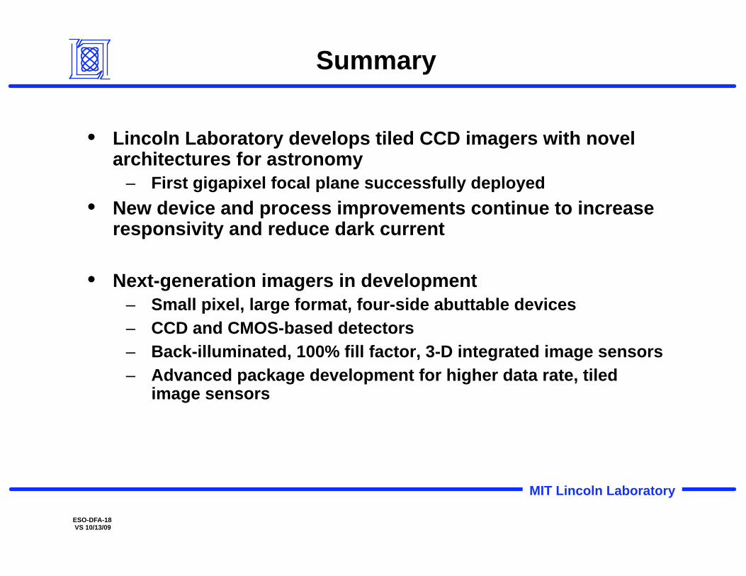
Summary
• Lincoln Laboratory develops tiled CCD imagers with novel architectures for astronomy
– First gigapixel focal plane successfully deployed
• New device and process improvements continue to increase responsivity and reduce dark current
• Next-generation imagers in development
– Small pixel, large format, four-side abuttable devices
– CCD and CMOS-based detectors
– Back-illuminated, 100% fill factor, 3-D integrated image sensors
– Advanced package development for higher data rate, tiled image sensors

MIT Lincoln Laboratory ESO-DFA-19 VS 10/13/09
Acknowledgments
Design Brian Aull
Bob Berger
Chang-Lee Chen
Michael Cooper Brad Felton
Kay Johnson
Keith Percival
Dennis Rathman
Bruce Wheeler
Microelectronics Lab
Doug Young
Andy Loomis
Chenson Chen
Jeff Knecht Donna Yost
Kevin Newcomb
Keith Warner
Dave Astolfi
Vladimir Bolkhovsky Ken Belanger
Desi Biasella
Laurie Briere
Marc Brunelle
John Burke Joe Ciampi
Jeff Decaprio
Diane DeCastro
Charlie Doherty
Pascale Gouker Yvette Grinbush
Paul Healey
Bob Healey
Denise Holohan
Testing Harry Clark
David Craig
William McGonagle
Dan O’Mara Tony Soares
Microelectronics Lab
Sal Ieni
John Jarmalowicz
Scott Ladd
Renée Lambert Debbie Landers
Jim Lawless
Jamie Mongiello
Chuck Monoxelos
Alan O’Dea John Pentoliros
Segundo Pichardo
Joe Powers
Sandra Roy
Angel Reinold Dolly Shibles
Chris Weinberg
Peter O’Brien
Wendy Ruth
T.J. Wlodarczak C. Keast (Solid State Div.)
D. Shaver (Solid State Div.)

MIT Lincoln Laboratory ESO-DFA-20 VS 10/13/09
Backup

MIT Lincoln Laboratory ESO-DFA-21 VS 10/13/09
Tile Block Diagram
• Vertically stacked
• Pixel readout on Tier-2
• Timing control in Stack
• 64-ch 12-b pipelined ADC
• Digital output
Light
MIT Lincoln Laboratory ESO-DFA-22 VS 10/13/09
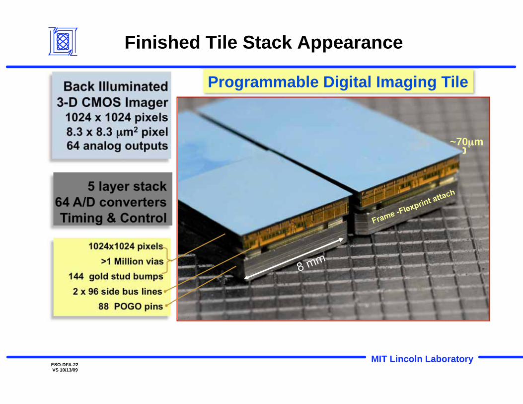
Finished Tile Stack Appearance
Back Illuminated
3-D CMOS Imager 1024 x 1024 pixels
8.3 x 8.3 μm2 pixel 64 analog outputs ~70μm
144 gold stud bumps
88 POGO pins
2 x 96 side bus lines
>1 Million vias
1024x1024 pixels
5 layer stack
64 A/D converters
Timing & Control
Programmable Digital Imaging Tile